JP5376865B2 - Solid-state imaging device and electronic imaging device - Google Patents
Solid-state imaging device and electronic imaging device Download PDFInfo
- Publication number
- JP5376865B2 JP5376865B2 JP2008210528A JP2008210528A JP5376865B2 JP 5376865 B2 JP5376865 B2 JP 5376865B2 JP 2008210528 A JP2008210528 A JP 2008210528A JP 2008210528 A JP2008210528 A JP 2008210528A JP 5376865 B2 JP5376865 B2 JP 5376865B2
- Authority
- JP
- Japan
- Prior art keywords
- solid
- imaging device
- state imaging
- translucent member
- holding member
- Prior art date
- Legal status (The legal status is an assumption and is not a legal conclusion. Google has not performed a legal analysis and makes no representation as to the accuracy of the status listed.)
- Expired - Fee Related
Links
- 238000003384 imaging method Methods 0.000 title claims description 141
- 239000000853 adhesive Substances 0.000 claims description 9
- 230000001070 adhesive effect Effects 0.000 claims description 9
- 239000000463 material Substances 0.000 claims description 8
- 230000001681 protective effect Effects 0.000 claims description 7
- 125000006850 spacer group Chemical group 0.000 claims description 7
- 239000010935 stainless steel Substances 0.000 claims description 3
- 229910001220 stainless steel Inorganic materials 0.000 claims description 3
- 229910001030 Iron–nickel alloy Inorganic materials 0.000 claims 1
- 239000007787 solid Substances 0.000 claims 1
- 230000003287 optical effect Effects 0.000 description 25
- 239000011347 resin Substances 0.000 description 9
- 229920005989 resin Polymers 0.000 description 9
- 238000000034 method Methods 0.000 description 8
- 238000007789 sealing Methods 0.000 description 8
- XEEYBQQBJWHFJM-UHFFFAOYSA-N Iron Chemical compound [Fe] XEEYBQQBJWHFJM-UHFFFAOYSA-N 0.000 description 4
- 229910045601 alloy Inorganic materials 0.000 description 4
- 239000000956 alloy Substances 0.000 description 4
- 239000002184 metal Substances 0.000 description 4
- 229910052751 metal Inorganic materials 0.000 description 4
- 239000011888 foil Substances 0.000 description 3
- 229910000640 Fe alloy Inorganic materials 0.000 description 2
- 229910000990 Ni alloy Inorganic materials 0.000 description 2
- 239000004855 amber Substances 0.000 description 2
- 230000015556 catabolic process Effects 0.000 description 2
- 239000004020 conductor Substances 0.000 description 2
- 239000011521 glass Substances 0.000 description 2
- 239000012212 insulator Substances 0.000 description 2
- 229910000833 kovar Inorganic materials 0.000 description 2
- 229910000889 permalloy Inorganic materials 0.000 description 2
- 239000004033 plastic Substances 0.000 description 2
- 229920003023 plastic Polymers 0.000 description 2
- 239000000758 substrate Substances 0.000 description 2
- 239000004593 Epoxy Substances 0.000 description 1
- 239000004642 Polyimide Substances 0.000 description 1
- -1 SUS430 and SUS304 Inorganic materials 0.000 description 1
- 239000000919 ceramic Substances 0.000 description 1
- 238000005553 drilling Methods 0.000 description 1
- 230000009977 dual effect Effects 0.000 description 1
- 230000000694 effects Effects 0.000 description 1
- 230000004907 flux Effects 0.000 description 1
- 238000010030 laminating Methods 0.000 description 1
- 239000007769 metal material Substances 0.000 description 1
- 150000002739 metals Chemical class 0.000 description 1
- 239000002245 particle Substances 0.000 description 1
- 230000002093 peripheral effect Effects 0.000 description 1
- 238000005498 polishing Methods 0.000 description 1
- 229920001721 polyimide Polymers 0.000 description 1
- 238000004080 punching Methods 0.000 description 1
- 239000010453 quartz Substances 0.000 description 1
- VYPSYNLAJGMNEJ-UHFFFAOYSA-N silicon dioxide Inorganic materials O=[Si]=O VYPSYNLAJGMNEJ-UHFFFAOYSA-N 0.000 description 1
- 229910000679 solder Inorganic materials 0.000 description 1
- 238000005476 soldering Methods 0.000 description 1
- 230000003746 surface roughness Effects 0.000 description 1
Images


Classifications
-
- H—ELECTRICITY
- H01—ELECTRIC ELEMENTS
- H01L—SEMICONDUCTOR DEVICES NOT COVERED BY CLASS H10
- H01L27/00—Devices consisting of a plurality of semiconductor or other solid-state components formed in or on a common substrate
- H01L27/14—Devices consisting of a plurality of semiconductor or other solid-state components formed in or on a common substrate including semiconductor components sensitive to infrared radiation, light, electromagnetic radiation of shorter wavelength or corpuscular radiation and specially adapted either for the conversion of the energy of such radiation into electrical energy or for the control of electrical energy by such radiation
- H01L27/144—Devices controlled by radiation
- H01L27/146—Imager structures
- H01L27/14601—Structural or functional details thereof
- H01L27/14618—Containers
-
- H—ELECTRICITY
- H01—ELECTRIC ELEMENTS
- H01L—SEMICONDUCTOR DEVICES NOT COVERED BY CLASS H10
- H01L27/00—Devices consisting of a plurality of semiconductor or other solid-state components formed in or on a common substrate
- H01L27/14—Devices consisting of a plurality of semiconductor or other solid-state components formed in or on a common substrate including semiconductor components sensitive to infrared radiation, light, electromagnetic radiation of shorter wavelength or corpuscular radiation and specially adapted either for the conversion of the energy of such radiation into electrical energy or for the control of electrical energy by such radiation
- H01L27/144—Devices controlled by radiation
- H01L27/146—Imager structures
- H01L27/14683—Processes or apparatus peculiar to the manufacture or treatment of these devices or parts thereof
-
- H—ELECTRICITY
- H04—ELECTRIC COMMUNICATION TECHNIQUE
- H04N—PICTORIAL COMMUNICATION, e.g. TELEVISION
- H04N23/00—Cameras or camera modules comprising electronic image sensors; Control thereof
- H04N23/50—Constructional details
- H04N23/54—Mounting of pick-up tubes, electronic image sensors, deviation or focusing coils
-
- H—ELECTRICITY
- H04—ELECTRIC COMMUNICATION TECHNIQUE
- H04N—PICTORIAL COMMUNICATION, e.g. TELEVISION
- H04N23/00—Cameras or camera modules comprising electronic image sensors; Control thereof
- H04N23/50—Constructional details
- H04N23/55—Optical parts specially adapted for electronic image sensors; Mounting thereof
-
- H—ELECTRICITY
- H01—ELECTRIC ELEMENTS
- H01L—SEMICONDUCTOR DEVICES NOT COVERED BY CLASS H10
- H01L2924/00—Indexing scheme for arrangements or methods for connecting or disconnecting semiconductor or solid-state bodies as covered by H01L24/00
- H01L2924/0001—Technical content checked by a classifier
- H01L2924/0002—Not covered by any one of groups H01L24/00, H01L24/00 and H01L2224/00
-
- Y—GENERAL TAGGING OF NEW TECHNOLOGICAL DEVELOPMENTS; GENERAL TAGGING OF CROSS-SECTIONAL TECHNOLOGIES SPANNING OVER SEVERAL SECTIONS OF THE IPC; TECHNICAL SUBJECTS COVERED BY FORMER USPC CROSS-REFERENCE ART COLLECTIONS [XRACs] AND DIGESTS
- Y10—TECHNICAL SUBJECTS COVERED BY FORMER USPC
- Y10T—TECHNICAL SUBJECTS COVERED BY FORMER US CLASSIFICATION
- Y10T156/00—Adhesive bonding and miscellaneous chemical manufacture
- Y10T156/10—Methods of surface bonding and/or assembly therefor
Landscapes
- Engineering & Computer Science (AREA)
- Physics & Mathematics (AREA)
- Power Engineering (AREA)
- General Physics & Mathematics (AREA)
- Electromagnetism (AREA)
- Condensed Matter Physics & Semiconductors (AREA)
- Computer Hardware Design (AREA)
- Microelectronics & Electronic Packaging (AREA)
- Signal Processing (AREA)
- Multimedia (AREA)
- Solid State Image Pick-Up Elements (AREA)
- Transforming Light Signals Into Electric Signals (AREA)
- Studio Devices (AREA)
- Camera Bodies And Camera Details Or Accessories (AREA)
Description
本発明は、CCDやCMOS等の固体撮像装置及びそれを搭載した電子撮像装置に関するものである。 The present invention relates to a solid-state imaging device such as a CCD or CMOS and an electronic imaging device equipped with the same.
図7は従来例の固体撮像装置の断面図を示す。従来の固体撮像装置にはセラミックや樹脂材料等からなるDIP(Dual Inline Package)やSOP(Small Outline Package)が広く用いられている。 FIG. 7 is a sectional view of a conventional solid-state imaging device. In conventional solid-state imaging devices, DIP (Dual Inline Package) and SOP (Small Outline Package) made of ceramic or resin material are widely used.
図7に示すように固体撮像素子601の電極と、パッケージに形成されたリードフレーム620とは、Au線等のボンディングワイヤ619で接続されている。また、透光性部材603は固体撮像素子601の受光面側のパッケージ表面に接着されている。このような固体撮像装置を用いたデジタルカメラやビデオカメラ等の電子撮像装置は、その組立てを行う際、固体撮像素子と光学ファインダの相対的位置関係の調整及び固体撮像素子と撮像ピント方向の位置調整が必要である。
As shown in FIG. 7, the electrode of the solid-
この調整においては、
(1)ピント方向の位置調整、
(2)(3)片ボケ防止の為の上下及び左右チルト調整、
(4)(5)画角合わせの為の水平及び垂直方向の調整、
(6)傾き回転調整が必要であり、少なくとも6軸調整が必要とされる。このような固体撮像装置は、特開平11−261904号公報(特許文献1)や特開2000−333050号公報(特許文献2)に記載されている。
(1) Position adjustment in the focus direction,
(2) (3) Up / down and left / right tilt adjustment to prevent one-side blur,
(4) (5) Horizontal and vertical adjustment for angle of view,
(6) Tilt rotation adjustment is required, and at least 6-axis adjustment is required. Such a solid-state imaging device is described in Japanese Patent Application Laid-Open No. 11-261904 (Patent Document 1) and Japanese Patent Application Laid-Open No. 2000-33050 (Patent Document 2).
上記従来の固体撮像装置では、電子撮像装置に組み込む際の6軸調整が固体撮像装置1個毎に必要であり、非常に作業時間のかかる工程となっている。その為に電子撮像装置自体のコストを押し上げている。 In the conventional solid-state imaging device, 6-axis adjustment is required for each solid-state imaging device when it is incorporated into an electronic imaging device, which is a very time-consuming process. For this reason, the cost of the electronic imaging device itself is increased.
そもそも6軸調整が必要となる要因は、固体撮像素子をパッケージに接着固定するダイボンディング工程にある。即ち、ダイボンディング装置ヘッドの水平分解能、垂直分解能、回転分解能に限界があり、固体撮像装置の位置の水平垂直方向及び回転方向にバラツキが生じることにある。 In the first place, the factor that requires 6-axis adjustment is the die bonding process for bonding and fixing the solid-state imaging device to the package. That is, there is a limit to the horizontal resolution, vertical resolution, and rotational resolution of the die bonding apparatus head, and there is a variation in the horizontal and vertical directions and the rotational direction of the position of the solid-state imaging device.
別の要因として、パッケージ自体の寸法の個体差やパッケージに固体撮像素子が載るダイアタッチ面の反り等の要因に起因して、搭載した固体撮像素子が深さ方向のピントバラツキや上下左右チルトのバラツキが生じることにあった。 As another factor, due to factors such as individual differences in the dimensions of the package itself and warpage of the die attach surface on which the solid-state image sensor is mounted, the mounted solid-state image sensor has a depth variation in focus and vertical and horizontal tilt. There was a variation.
本発明の目的は、電子撮像装置に組み込む場合の作業時間のかかる6軸調整を不要にでき、組立を簡単且つ短時間で行うことが可能な固体撮像装置及び電子撮像装置を提供することにある。 An object of the present invention is to provide a solid-state imaging device and an electronic imaging device that can eliminate the need for six-axis adjustment that requires work time when incorporated in an electronic imaging device and can be assembled easily and in a short time. .
本発明は、固体撮像素子と、少なくとも一部の領域が前記固体撮像素子より延出した延出部を有する透光性部材と、前記透光性部材を保持する保持部材とを有し、前記透光性部材は前記固体撮像素子の受光面と一定間隔をおいて平行に固定され、前記保持部材は、上面と、下面と、前記上面から前記下面まで貫通して前記固体撮像素子を収納可能な空間を囲む側面と、前記空間を囲む側面の一部であって前記空間へ向かって突き出す部分で構成された位置決め部とを有しており、前記位置決め部に前記固体撮像素子の側面が突き当てられ、前記延出部が前記保持部材に固定されており、前記固体撮像素子の裏面が保護部材で覆われていることを特徴とする。 The present invention includes a solid-state imaging device, a translucent member having an extension portion in which at least a part of the region extends from the solid-state imaging device, and a holding member that holds the translucent member, The translucent member is fixed in parallel with the light receiving surface of the solid-state image sensor at a predetermined interval, and the holding member can be stored in the solid-state image sensor through the upper surface, the lower surface, and the upper surface to the lower surface. And a positioning part that is a part of the side surface that surrounds the space and that protrudes toward the space, and the side surface of the solid-state imaging element projects into the positioning part. The extending portion is fixed to the holding member, and the back surface of the solid-state imaging device is covered with a protective member .
本発明によれば、固体撮像装置を電子撮像装置に組み込む際に必要であった6軸調整作業を不要にすることが可能となる。そのため、組立作業を著しく簡単にでき、電子撮像装置を安価に作製することが可能となる。 According to the present invention, it is possible to eliminate the 6-axis adjustment work that was necessary when the solid-state imaging device was incorporated into the electronic imaging device. Therefore, the assembling work can be remarkably simplified, and the electronic imaging device can be manufactured at a low cost.
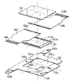
次に、発明を実施するための最良の形態について図面を参照して詳細に説明する。図1は本発明に係る固体撮像装置の一実施形態を示す平面図、図2は固体撮像装置を構成する各部を分解して示す分解斜視図である。また、図3(a)は図1のA−A線方向から見た断面図、図3(b)は図1のB−B線方向から見た断面図である。図3(a)は固体撮像素子と配線基板との接続部を詳細に示すものである。 Next, the best mode for carrying out the invention will be described in detail with reference to the drawings. FIG. 1 is a plan view showing an embodiment of a solid-state imaging device according to the present invention, and FIG. 2 is an exploded perspective view showing each part constituting the solid-state imaging device in an exploded manner. 3A is a cross-sectional view seen from the AA line direction of FIG. 1, and FIG. 3B is a cross-sectional view seen from the BB line direction of FIG. FIG. 3A shows in detail a connection portion between the solid-state imaging device and the wiring board.
図中101はCCDやCMOS等の固体撮像素子であり、その一主面上に受光領域101aが形成されている。固体撮像素子101の受光領域101aの周辺部であって対向する2辺にわたる領域には固体撮像素子101の入出力信号に寄与する電極101bが形成されている。固体撮像素子101の上面には透光性部材103が配置されている。固体撮像素子101に接続する透光性部材103としては、主にガラスや水晶が用いられ、固体撮像素子101の受光面と一定間隔になるように配置されている。
In the figure,
固体撮像素子101の受光面と、透光性部材103とを一定間隔をおいて平行に配置する方法としては、特に限定は無いが、例えば、図3(a)、図3(b)に示すように球状のスペーサ部材106を使用する方法がある。また、柱状のスペーサ部材(不図示)を使用することでも容易に実現可能である。
A method for arranging the light receiving surface of the solid-
更に、スペーサ部材106の周囲に接着剤107を介在させることで、一定間隔を保ったまま容易に接着することが可能である。スペーサ部材106と接着剤107は、固体撮像素子101の4辺にわたり一様に形成され、固体撮像素子101の受光領域101aに侵入することがないように配置されている。
Furthermore, by interposing the
上記構成により、固体撮像素子101と透光性部材103とが一定間隔をおいて平行に配置される為、固体撮像素子101の受光面と透光性部材103との平行度及び固体撮像素子101の受光面と透光性部材103との距離を一定のものとして担保しうる。透光性部材103の大きさとしては、少なくとも一部の領域を固体撮像素子101から延出させた構造となっている。即ち、固体撮像素子101のサイズよりも少なくとも一部の領域を大きくしておくことが重要である。このように透光性部材103の少なくとも一部の領域を延出させておき、その領域を後述の保持部材102との接続に使用することで、位置精度を容易に確保することが可能である。
With the above configuration, since the solid-
また、透光性部材103は固体撮像素子101よりも全体が大きくても構わない。その際、図1に示すように電極101bが固体撮像素子101の対向する2辺に形成されている場合、電極101bが形成されていない対向する2辺側を固体撮像素子101のサイズよりも大きくするのが好ましい。また、電極101bが形成された対向する2辺側では固体撮像素子101の電極101bと受光領域101aとの間に透光性部材103の端面が位置するように小さくしておく形状がより好ましい。
Further, the entire
このような形状とすることで、固体撮像素子101に透光性部材103を配置した後でも電極101bが露出している為、透光性部材103の接着後に配線基板104を取り付けることが可能となる。配線基板104は透光性部材103を配置する前に取り付けることも勿論可能であるが、透光性部材103を先に配置することで固体撮像素子101が組立て環境にさらされる時間を短くすることが出来る。そのため、固体撮像素子101の受光領域101a上に付着するパーティクル等を防止することが出来る。
By adopting such a shape, since the
透光性部材103の厚みとしては、特に限定は無いが、0.1mmから2.0mmものが好適に使用される。配線基板104は図3(a)に示すようにポリイミド等のベースフィルム104eにCu等の導体箔104cをラミネートし、端子部やはんだ付け部以外にはソルダーレジスト等の絶縁体104dを被覆して保護した構成のフレキシブルプリント基板等からなる。
The thickness of the
固体撮像素子101の電極101bと電気的な接続をとる導体箔104cには、図2に示すように固体撮像素子101に形成された電極101bと同ピッチで配線されたインナリード104aが形成されている。不図示の電子撮像装置本体の基板と電気的な接続をとるアウタ側にはアウタリード104bが形成されている。
As shown in FIG. 2, the
固体撮像素子101に形成された電極101bには、図3(a)に示すように配線基板104のインナリード104aとの接続の為にAu等のスタッドバンプ108が形成されている。スタッドバンプ108にはインナリード104aとの接続を容易に行う為に上面に平坦化処理を施すことが好ましい。スタッドバンプ108とインナリード104aとの相対位置を合わせた後、ギャングボンディングやシングルポイントボンディング等により電気的な接続がとられる。
A
固体撮像素子101に透光性部材103と配線基板104を取り付けた後に保持部材102を取り付ける。保持部材102は透光性部材103を保持すると同時に図2に示すように固体撮像素子101を収納可能な空間102dを有する。また、固体撮像素子101を位置決めする為の位置決め部102aを有する部品である。以下、保持部材102について詳述する。
After the
保持部材102は、図2に示すようにその中央に固体撮像素子101が収納可能なように空間102dが形成された板状の部材である。保持部材102には位置決め部102aが設けられている。位置決め部102aは保持部材102と一体であって、空間102dに突き出すように突起状に3点設けられている。
As shown in FIG. 2, the holding
保持部材102を構成する材料としては、剛性を有する材料であって、例えば、±50μm以下の寸法精度が得られる材料が好適である。平面性に関しても±30μm以内の加工精度が得られる材料が好適である。より好適には、平面度に関しては±10μm以下である。これらの特性を達成可能な材料としては、プラスチック、金属等適宜選択可能である。
As the material constituting the holding
プラスチックの場合には、剛性のある材料が好適であり、例えば、PC、ABS、POW、PP、PE、PPEE等が好適であるが、特に限定されるものではない。また、導電性が付与されていることが静電破壊の観点で好ましい。 In the case of plastic, a rigid material is preferable, and for example, PC, ABS, POW, PP, PE, PPEE, etc. are preferable, but there is no particular limitation. Moreover, it is preferable from a viewpoint of electrostatic breakdown that electroconductivity is provided.
金属の場合には、材質は例えば42アロイ、50アロイ、パーマロイ、コバール、アンバー、SUS430、SUS304等の鉄・ニッケル合金やステンレス鋼等が好適であるが、特に限定されるものではない。プレス加工にて所望の形状を得た後、研磨、ラップ加工等を行うことで、面粗さ、平面度を所望以下に抑える事も可能である。金属材料の場合には、導電率が高いので、固体撮像素子との接触時に静電破壊の影響をより防止することが可能な為、より好適である。 In the case of a metal, for example, 42 alloy, 50 alloy, permalloy, Kovar, amber, iron / nickel alloy such as SUS430 and SUS304, stainless steel, and the like are suitable, but not particularly limited. After obtaining a desired shape by press working, it is possible to suppress surface roughness and flatness to less than desired by performing polishing, lapping, or the like. In the case of a metal material, since the electrical conductivity is high, it is more preferable because the influence of electrostatic breakdown can be further prevented at the time of contact with the solid-state imaging device.
このような保持部材102に対して上述のように平行配置された固体撮像素子101と透光性部材103を取り付ける。取り付け方法としては、固体撮像素子101の側面を位置決め部102a(本実施形態では図2に示す3箇所の位置決め部102a)に突き当てる。同時に、透光性部材103の延出部の固体撮像素子の接着面側を保持部材102に密着させて接続を行う(図3(b)参照)。その場合、図3に示すように封止樹脂105によって透光性部材103を保持部材102に接着しても良いし、別途、接着剤を用いて接着しても良い。
The solid-
このような構成とすることで、保持部材102に対して平行に透光性部材103を取り付けることが出来る。透光性部材103と固体撮像素子101とは既に平行に接続されている為、保持部材102に対する固体撮像素子101の位置(ピント方向の位置)を一定にできる。また、片ボケ防止の為の上下左右チルトの位置を常に一定にすることができる。
With such a configuration, the
即ち、保持部材102を基準に透光性部材103と固体撮像素子101を平行に保って接続することにより、保持部材102に対する固体撮像素子101のピント方向位置(Z方向)…(1)の調整を完了する。同時に上下及び左右チルト…(2)(3)の3軸の調整を完了する。
That is, by adjusting the holding
更に、透光性部材103に接続された固体撮像素子101の側面を、保持部材102に形成された位置決め部102aに接触(突き当て)させて接続する為、保持部材102に対する固体撮像素子101の水平垂直方向の位置及び傾き回転方向の位置を常に一定にできる。即ち、水平垂直方向(XY方向)…(4)(5)、及び回転方向(θ)…(6)の3軸の調整を完了することができる。これら(1)〜(6)は背景技術で説明した(1)〜(6)と同様である。
Furthermore, the side surface of the solid-
本発明の構造では、この時点で保持部材102に対する固体撮像素子101の6軸調整が全て完了している状態となる。また、保持部材102には少なくとも取り付け穴からなる固定手段を形成することが望ましい。また、取り付け穴に加えて位置決め穴を設けても構わない。
In the structure of the present invention, all the six-axis adjustments of the solid-
本実施形態では、図1、図2に示すように保持部材102に位置決め穴102cと取り付け穴102bが設けられており、位置決め穴102cが2個、取り付け穴102bが3個の例を示す。これらの穴は、公知のドリル加工や打ち抜き加工により、保持部材102に対して精度よく形成することが可能である。
In this embodiment, as shown in FIGS. 1 and 2, the holding
従って、保持部材102の取り付け穴位置に対して固体撮像素子101の位置を一義的に決定することが可能であり、常に一定状態の位置関係を保った固体撮像装置を提供することが可能である。
Therefore, it is possible to uniquely determine the position of the solid-
また、固体撮像装置側に固定手段(取り付け穴102b)を形成し、デジタルカメラやデジタルビデオカメラ等の電子撮像装置側に固定手段に対応する接続部(取り付け穴等)を精度よく形成しておく。そうすることで、本発明の固体撮像装置を固定手段を使って電子撮像装置に接続するだけで、容易に電子撮像装置に対する固体撮像装置の所望の精度を得ることが可能である。 Further, fixing means (attachment holes 102b) are formed on the solid-state imaging device side, and connection portions (attachment holes and the like) corresponding to the fixing means are accurately formed on the electronic imaging device side such as a digital camera or a digital video camera. . By doing so, it is possible to easily obtain the desired accuracy of the solid-state imaging device with respect to the electronic imaging device simply by connecting the solid-state imaging device of the present invention to the electronic imaging device using a fixing means.
その際、上述のように保持部材102に対して固体撮像素子101の6軸調整は完了している。そのため、本発明の固体撮像装置を保持部材102に形成された固定手段(取り付け穴102b)を用いて電子撮像装置に組み込むことにより、6軸調整を行うことなく、簡単に組み込むことが可能となる。
At that time, as described above, the six-axis adjustment of the solid-
ここで、図3に示す封止樹脂105はスペーサ部材106及び接着剤107の外周を覆うように形成されている。また、図示していないが、固体撮像素子101の裏面(非受光面側)を完全に覆うように形成してもよい。封止樹脂105は、例えば、耐湿性に優れたエポキシ系の封止樹脂であって、特に限定は無いが、熱あるいは紫外線またはその併用で硬化するタイプの封止樹脂が好適である。
Here, the sealing
このように封止樹脂105を形成することで、固体撮像素子の耐湿性と、接続部材である導体箔104cの機械的・電気的な接続信頼性を向上させることができる。固体撮像素子101の裏面を覆う手段としては、封止樹脂105を使用する方法の他に、保護部材112を接着しても良い。
By forming the sealing
図4は固体撮像素子101の裏面(非受光面側)を保護部材112で覆った実施形態を示す断面図である。図4では図1、図2等と同一部分には同一符号を付している。保護部材112の材料には、特に限定は無いが、例えば、熱伝導率の高い42アロイ、50アロイ、パーマロイ、コバール、アンバー、SUS430、SUS304等の鉄・ニッケル合金やステンレス鋼の金属が好適に用いられる。そうすることで、放熱板の役割を担うこともできる。
FIG. 4 is a cross-sectional view showing an embodiment in which the back surface (non-light-receiving surface side) of the solid-
また、保護部材112は保持部材102と接着させているが、固体撮像素子101の保護と放熱を目的とする場合には固体撮像素子101の裏面と保護部材312を熱電度率の高い接着剤を用いて接着することが好ましい。
In addition, the
本発明の固体撮像装置は、直接、電子撮像装置に取り付けて固定する場合もあるが、一旦、別のユニット部品に取り付けた後、ユニット部品を介して電子撮像装置に固定しても同様の効果を得ることができる。ユニット部品については、特に限定は無いが、例えば、本発明の固体撮像装置に光学ローパスフィルタ等の光学部品を搭載したユニット部品が挙げられる。 The solid-state imaging device of the present invention may be directly attached and fixed to the electronic imaging device. However, the same effect can be obtained if the solid-state imaging device is once attached to another unit component and then fixed to the electronic imaging device via the unit component. Can be obtained. Although there is no limitation in particular about a unit component, For example, the unit component which mounts optical components, such as an optical low-pass filter, in the solid-state imaging device of this invention is mentioned.
図5は固体撮像装置に光学ローパスフィルタ等の光学部品を載置したユニット(以下、固体撮像装置ユニットと呼ぶ)の一例を示す。図5では図1乃至図4と同一部分には同一符号を付している。図中409は光学ローパスフィルタ、410は本発明の固体撮像装置に光学ローパスフィルタ409を搭載した固体撮像装置ユニットである。フィルタ409は赤外吸収ガラスとダイクロイックミラーから成る赤外カットフィルタと被写体像を水平方向、垂直方向に分離する分離板と位相板から成るローパスフィルタにより構成されている。
FIG. 5 shows an example of a unit (hereinafter referred to as a solid-state imaging device unit) in which an optical component such as an optical low-pass filter is mounted on the solid-state imaging device. In FIG. 5, the same parts as those in FIGS. 1 to 4 are denoted by the same reference numerals. In the figure,
光学ローパスフィルタ409は、光学ローパスフィルタ保持部材411に固定されており、光学ローパスフィルタ保持部材411には固体撮像装置に設けられた取り付け穴102bに対応する箇所に取り付け穴411aが形成されている。
The optical low-
光学ローパスフィルタ409を備えた光学ローパスフィルタ保持部材411は固体撮像装置の保持部材102を基準として、取り付け穴102b及び411aの相対位置合わせにより接続されている。光学ローパスフィルタ保持部材411を精度よく形成しておくことにより、固体撮像装置ユニット410においては固体撮像装置と光学ローパスフィルタ409も一定状態の位置関係を保つことが可能となる。
The optical low-pass
図6は図5に示す固体撮像素子ユニット410をカメラ(電子撮像装置)に組み込んだ例を示す図である。図6では図5と同一部分には同一符号を付している。図中513はカメラ本体、514はシャッターユニットである。515はミラーであり、観察状態と撮像状態に応じて撮像経路へ斜設或いは退去される。
FIG. 6 is a view showing an example in which the solid-state
観察状態ではミラー515は撮像光路に斜設された状態にあり、ミラー515で反射した光束をカメラ本体上方へ向けて反射し、ペンタプリズム516、ファインダ光学系517を介して観察画像をファインダより観察できるように構成されている。
In the observation state, the
また、撮像状態ではミラー515は撮像光路から退去された状態にあり、光束はシャッターユニット514が開いている間に固体撮像装置ユニット410の構成部品である光学ローパスフィルタ409を介して固体撮像装置ユニット410に入射する。
In the imaging state, the
固体撮像装置ユニット410はカメラ本体の一部を成すシャッターユニット514に接続されている。シャッターユニット514には固体撮像装置の取り付け穴102bに対応する箇所に固体撮像装置ユニット接続用の取り付け穴514aが設けられている。取り付け穴514aは光学ローパスフィルタ保持部材411に設けられた取り付け穴411aと相対位置関係が同一でなくても良いが、同一としても良い。その場合には一度に光学ローパスフィルタ保持部材409とシャッターユニット514を固体撮像装置に固定することが出来る。
The solid-state
カメラに本体に組み込む場合においても、固体撮像装置ユニット410の被接続側を精度よく作製しておけば、固体撮像装置ユニット410を固定するだけで精度よく光学系を構成することができ、特に調整をする必要は無い。即ち、保持部材102に対する固体撮像素子の6軸調整は完了しており、固体撮像装置ユニット410をカメラ本体に組み込む場合にも固体撮像素子と光学ファインダとの相対位置関係や撮像ピント方向の調整は不要である。そのため、調整工程を大幅に削減でき、安価な電子撮像装置を提供することが可能となる。
Even in the case of being incorporated in the camera body, if the connected side of the solid-state
101 固体撮像素子
101a 受光領域
101b 電極
102 保持部材
102a 位置決め部
102b、411a 取り付け穴
102c 位置決め穴
102d 空間
103 透光性部材
104 配線基板
104a インナリード
104b アウタリード
104c 導体箔
104d 絶縁体
104e ベースフィルム
105 封止樹脂
106 スペーサ部材
107 接着剤
108 スタッドバンプ
112 保護部材
409 光学ローパスフィルタ
410 固体撮像装置ユニット
411 光学ローパスフィルタ保持部材
513 カメラ本体
514 シャッターユニット
515 ミラー
516 ペンタプリズム
517 ファインダ光学系
DESCRIPTION OF
Claims (14)
前記透光性部材は前記固体撮像素子の受光面と一定間隔をおいて平行に固定され、
前記保持部材は、上面と、下面と、前記上面から前記下面まで貫通して前記固体撮像素子を収納可能な空間を囲む側面と、前記空間を囲む側面の一部であって前記空間へ向かって突き出す部分で構成された位置決め部とを有しており、
前記位置決め部に前記固体撮像素子の側面が突き当てられ、前記延出部が前記保持部材に固定されており、
前記固体撮像素子の裏面が保護部材で覆われていることを特徴とする固体撮像装置。 A solid-state imaging device, a translucent member having an extended portion in which at least a part of the region extends from the solid-state imaging device, and a holding member that holds the translucent member,
The translucent member is fixed in parallel with the light receiving surface of the solid-state image sensor at a certain interval,
The holding member is an upper surface, a lower surface, a side surface that surrounds the space that can penetrate from the upper surface to the lower surface and can accommodate the solid-state imaging device, and a part of the side surface that surrounds the space, toward the space. A positioning part composed of a protruding part,
A side surface of the solid-state imaging device is abutted against the positioning part, and the extension part is fixed to the holding member ,
A solid-state imaging device, wherein a back surface of the solid-state imaging element is covered with a protective member .
前記透光性部材と前記固体撮像素子とが接着剤により接着されており、
前記固体撮像素子の受光面と前記電極との間に、前記透光性部材と前記固体撮像素子と接着する接着剤が位置することを特徴とする請求項1に記載の固体撮像装置。 Electrodes are formed on two opposing sides of the solid-state image sensor,
The translucent member and the solid-state imaging device are bonded with an adhesive,
The solid-state imaging device according to claim 1, wherein an adhesive that adheres to the translucent member and the solid-state imaging element is located between a light receiving surface of the solid-state imaging element and the electrode.
Priority Applications (3)
| Application Number | Priority Date | Filing Date | Title |
|---|---|---|---|
| JP2008210528A JP5376865B2 (en) | 2008-08-19 | 2008-08-19 | Solid-state imaging device and electronic imaging device |
| US12/503,888 US8643773B2 (en) | 2008-08-19 | 2009-07-16 | Manufacturing method of solid-state imaging apparatus, solid-state imaging apparatus, and electronic imaging apparatus |
| US14/142,219 US9111827B2 (en) | 2008-08-19 | 2013-12-27 | Manufacturing method of solid-state imaging apparatus, solid-state imaging apparatus, and electronic imaging apparatus |
Applications Claiming Priority (1)
| Application Number | Priority Date | Filing Date | Title |
|---|---|---|---|
| JP2008210528A JP5376865B2 (en) | 2008-08-19 | 2008-08-19 | Solid-state imaging device and electronic imaging device |
Related Child Applications (1)
| Application Number | Title | Priority Date | Filing Date |
|---|---|---|---|
| JP2013162234A Division JP5631457B2 (en) | 2013-08-05 | 2013-08-05 | Solid-state imaging device and electronic imaging device |
Publications (2)
| Publication Number | Publication Date |
|---|---|
| JP2010050518A JP2010050518A (en) | 2010-03-04 |
| JP5376865B2 true JP5376865B2 (en) | 2013-12-25 |
Family
ID=41696014
Family Applications (1)
| Application Number | Title | Priority Date | Filing Date |
|---|---|---|---|
| JP2008210528A Expired - Fee Related JP5376865B2 (en) | 2008-08-19 | 2008-08-19 | Solid-state imaging device and electronic imaging device |
Country Status (2)
| Country | Link |
|---|---|
| US (2) | US8643773B2 (en) |
| JP (1) | JP5376865B2 (en) |
Cited By (1)
| Publication number | Priority date | Publication date | Assignee | Title |
|---|---|---|---|---|
| US11894407B2 (en) | 2018-06-29 | 2024-02-06 | Sony Semiconductor Solutions Corporation | Imaging apparatus and electronic device |
Families Citing this family (5)
| Publication number | Priority date | Publication date | Assignee | Title |
|---|---|---|---|---|
| CN102714211B (en) * | 2010-08-04 | 2015-06-17 | 松下电器产业株式会社 | Solid-state image pickup device |
| JP6057538B2 (en) * | 2012-04-27 | 2017-01-11 | キヤノン株式会社 | Imaging device |
| CN103605256A (en) * | 2013-11-28 | 2014-02-26 | 上海纬而视科技股份有限公司 | Electric device of DLP six-axis adjusting platform |
| US10580811B2 (en) * | 2015-11-24 | 2020-03-03 | Sony Corporation | Image pickup element package having a supporting resin frame with a thermally conductive portion including electronic components, and associated image pickup apparatus |
| JP6443494B2 (en) * | 2017-05-25 | 2018-12-26 | 株式会社ニコン | Imaging unit and imaging apparatus |
Family Cites Families (23)
| Publication number | Priority date | Publication date | Assignee | Title |
|---|---|---|---|---|
| JPS63131463A (en) | 1986-11-11 | 1988-06-03 | ザ テイラ−−ウインフイ−ルド コ−ポレイシヨン | Battery mutual cell junction by induction heating |
| JPH0528858Y2 (en) * | 1987-02-19 | 1993-07-23 | ||
| JPH04235475A (en) * | 1991-01-10 | 1992-08-24 | Olympus Optical Co Ltd | Solid-state image pickup device |
| JP2865908B2 (en) | 1991-08-13 | 1999-03-08 | 鐘紡株式会社 | Transparent polyester disc substrate |
| JP2600527Y2 (en) * | 1991-11-01 | 1999-10-12 | オリンパス光学工業株式会社 | Mounting device for image sensor |
| JP3207319B2 (en) | 1993-05-28 | 2001-09-10 | 株式会社東芝 | Photoelectric conversion device and method of manufacturing the same |
| US6654064B2 (en) * | 1997-05-23 | 2003-11-25 | Canon Kabushiki Kaisha | Image pickup device incorporating a position defining member |
| JP2000333050A (en) | 1999-05-20 | 2000-11-30 | Canon Inc | Image pickup element mount device |
| JP4282226B2 (en) * | 2000-12-28 | 2009-06-17 | オリンパス株式会社 | camera |
| CN1185915C (en) * | 2001-06-13 | 2005-01-19 | 佳能株式会社 | Flexible substrate, semiconductor device, camera device and X-ray camera system |
| JP2003163342A (en) | 2001-11-29 | 2003-06-06 | Olympus Optical Co Ltd | Solid state imaging device and its manufacturing method |
| KR20050026492A (en) * | 2002-07-18 | 2005-03-15 | 코닌클리즈케 필립스 일렉트로닉스 엔.브이. | Camera module, camera system and method of manufacturing a camera module |
| TW579169U (en) * | 2003-05-28 | 2004-03-01 | Benq Corp | Optical module for a digital camera |
| JP2005039152A (en) * | 2003-07-18 | 2005-02-10 | Shinko Electric Ind Co Ltd | Method of manufacturing semiconductor device |
| JP4024763B2 (en) * | 2004-01-19 | 2007-12-19 | オリンパス株式会社 | Endoscopic imaging apparatus and method for assembling endoscopic imaging apparatus |
| JP4375116B2 (en) * | 2004-04-02 | 2009-12-02 | パナソニック株式会社 | Imaging device |
| JP2006080961A (en) * | 2004-09-10 | 2006-03-23 | Konica Minolta Opto Inc | Image pickup device and portable terminal provided with the same |
| JP4555732B2 (en) * | 2005-05-24 | 2010-10-06 | オリンパスイメージング株式会社 | Imaging device |
| JP4673721B2 (en) * | 2005-10-21 | 2011-04-20 | 富士通セミコンダクター株式会社 | Imaging apparatus and manufacturing method thereof |
| GB0602883D0 (en) * | 2006-02-14 | 2006-03-22 | Art Materials Service Inc | Picture frame fixings |
| JP4702954B2 (en) * | 2006-03-09 | 2011-06-15 | キヤノン株式会社 | Imaging device |
| JP2007299929A (en) | 2006-04-28 | 2007-11-15 | Matsushita Electric Ind Co Ltd | Optical device, and optical device module employing it |
| CN101174643A (en) * | 2006-11-03 | 2008-05-07 | 鸿富锦精密工业(深圳)有限公司 | Image sensor encapsulation and image sensor module group using the same |
-
2008
- 2008-08-19 JP JP2008210528A patent/JP5376865B2/en not_active Expired - Fee Related
-
2009
- 2009-07-16 US US12/503,888 patent/US8643773B2/en not_active Expired - Fee Related
-
2013
- 2013-12-27 US US14/142,219 patent/US9111827B2/en not_active Expired - Fee Related
Cited By (1)
| Publication number | Priority date | Publication date | Assignee | Title |
|---|---|---|---|---|
| US11894407B2 (en) | 2018-06-29 | 2024-02-06 | Sony Semiconductor Solutions Corporation | Imaging apparatus and electronic device |
Also Published As
| Publication number | Publication date |
|---|---|
| US9111827B2 (en) | 2015-08-18 |
| US20140113399A1 (en) | 2014-04-24 |
| JP2010050518A (en) | 2010-03-04 |
| US20100045832A1 (en) | 2010-02-25 |
| US8643773B2 (en) | 2014-02-04 |
Similar Documents
| Publication | Publication Date | Title |
|---|---|---|
| JP6597729B2 (en) | Imaging unit and imaging apparatus | |
| TWI558200B (en) | Image capturing module and image capturing device | |
| JP5376865B2 (en) | Solid-state imaging device and electronic imaging device | |
| US8159595B2 (en) | Camera module having circuit component | |
| JP4225860B2 (en) | Digital camera | |
| JP2005216970A (en) | Optical device module, and manufacturing method therefor | |
| JP5913284B2 (en) | Device with optical module and support plate | |
| JP2007128995A (en) | Structure for mounting imaging element on fpc | |
| JP5730678B2 (en) | IMAGING DEVICE AND ELECTRONIC DEVICE USING THE SAME | |
| JP2008263550A (en) | Solid-state imaging device and manufacturing method therefor | |
| JP2004242166A (en) | Optical module, its manufacturing method, and electronic equipment | |
| JP7007888B2 (en) | 3D photoelectric imaging module | |
| WO2017090223A1 (en) | Image pickup element package, image pickup device, and method for manufacturing image pickup element package | |
| JP2010283760A (en) | Camera module and method of manufacturing the same | |
| US7612333B2 (en) | Imaging apparatus and photoelectric conversion element package retaining unit | |
| JP2009232159A (en) | Solid-state imaging apparatus, camera, and method of manufacturing them | |
| JP4745016B2 (en) | The camera module | |
| JP4169938B2 (en) | Solid-state image sensor holding block and solid-state image sensor mounting structure | |
| JP5631457B2 (en) | Solid-state imaging device and electronic imaging device | |
| JP5540465B2 (en) | Package body | |
| JP2008168042A (en) | Stacked mounting structure | |
| JP5978122B2 (en) | Camera mount structure and solid-state image sensor package | |
| JP2008263551A (en) | Solid-state imaging device and manufacturing method therefor | |
| JP2010080577A (en) | Semiconductor device | |
| JP2019050418A (en) | Imaging apparatus |
Legal Events
| Date | Code | Title | Description |
|---|---|---|---|
| RD04 | Notification of resignation of power of attorney |
Free format text: JAPANESE INTERMEDIATE CODE: A7424 Effective date: 20100201 |
|
| RD01 | Notification of change of attorney |
Free format text: JAPANESE INTERMEDIATE CODE: A7421 Effective date: 20100630 |
|
| A621 | Written request for application examination |
Free format text: JAPANESE INTERMEDIATE CODE: A621 Effective date: 20110801 |
|
| A977 | Report on retrieval |
Free format text: JAPANESE INTERMEDIATE CODE: A971007 Effective date: 20121116 |
|
| A131 | Notification of reasons for refusal |
Free format text: JAPANESE INTERMEDIATE CODE: A131 Effective date: 20121120 |
|
| A521 | Request for written amendment filed |
Free format text: JAPANESE INTERMEDIATE CODE: A523 Effective date: 20130121 |
|
| A131 | Notification of reasons for refusal |
Free format text: JAPANESE INTERMEDIATE CODE: A131 Effective date: 20130604 |
|
| A521 | Request for written amendment filed |
Free format text: JAPANESE INTERMEDIATE CODE: A523 Effective date: 20130805 |
|
| TRDD | Decision of grant or rejection written | ||
| A01 | Written decision to grant a patent or to grant a registration (utility model) |
Free format text: JAPANESE INTERMEDIATE CODE: A01 Effective date: 20130827 |
|
| A61 | First payment of annual fees (during grant procedure) |
Free format text: JAPANESE INTERMEDIATE CODE: A61 Effective date: 20130924 |
|
| LAPS | Cancellation because of no payment of annual fees |