JP5375503B2 - Bending vibration piece - Google Patents
Bending vibration piece Download PDFInfo
- Publication number
- JP5375503B2 JP5375503B2 JP2009233068A JP2009233068A JP5375503B2 JP 5375503 B2 JP5375503 B2 JP 5375503B2 JP 2009233068 A JP2009233068 A JP 2009233068A JP 2009233068 A JP2009233068 A JP 2009233068A JP 5375503 B2 JP5375503 B2 JP 5375503B2
- Authority
- JP
- Japan
- Prior art keywords
- piezoelectric film
- vibrating arm
- electrode
- bending vibration
- vibration piece
- Prior art date
- Legal status (The legal status is an assumption and is not a legal conclusion. Google has not performed a legal analysis and makes no representation as to the accuracy of the status listed.)
- Active
Links
Images


Abstract
Description
本発明は、振動腕を屈曲させるための圧電膜を備えた構成の屈曲振動片に関する。 The present invention relates to a bending vibration piece having a configuration including a piezoelectric film for bending a vibrating arm.
従来、屈曲振動片は、例えば特許文献1および特許文献2に開示されているように、振動腕の表面に圧電体素子を備えているものが開示されている。屈曲振動片は、それぞれの圧電体素子へ駆動電流を印加して、圧電体素子を変形させることにより、振動腕を所定方向へ屈曲させている。この場合、圧電体素子は、2つの電極で圧電膜を挟みこんだ構成のものであり、2つの電極に対して駆動電流を印加して圧電膜を変形させるようになっている。屈曲振動片は、圧電特性の良い膜である圧電膜を有する圧電体素子を振動腕に形成し、この圧電体素子を変形させて振動腕を屈曲させているため、振動腕に対する形状、寸法精度等の制約が少なくなる。さらに、圧電体素子を備えた屈曲振動片は、振動腕が圧電材以外であっても、振動腕の基材の特性を活かした屈曲振動を得ることが可能である。
Conventionally, as disclosed in
しかし、従来の技術では、振動腕の表面へ圧電膜を設け、この圧電膜の変形に応じて振動腕が屈曲する構成である。そのため、振動腕と圧電膜との密着性が不十分なことなどにより、振動腕と圧電膜との間に剥離等が生じた場合には、振動腕が所定の屈曲を行うことができなくなる、という課題があった。 However, in the conventional technique, a piezoelectric film is provided on the surface of the vibrating arm, and the vibrating arm is bent according to the deformation of the piezoelectric film. Therefore, when peeling or the like occurs between the vibrating arm and the piezoelectric film due to insufficient adhesion between the vibrating arm and the piezoelectric film, the vibrating arm cannot perform a predetermined bend, There was a problem.
本発明は、上記課題の少なくとも一部を解決するためになされたものであり、以下の適用例または形態として実現することが可能である。 SUMMARY An advantage of some aspects of the invention is to solve at least a part of the problems described above, and the invention can be implemented as the following application examples or forms.
[適用例1]本適用例に係る屈曲振動片は、基部と、該基部から突出して形成された振動腕と、を有する屈曲基板と、前記振動腕に形成された下部電極と、該下部電極に重ねて形成された圧電膜と、該圧電膜に重ねて形成された上部電極と、を備えている屈曲振動片であって、少なくとも前記屈曲基板と前記圧電膜との間に緩和層をさらに備え、該緩和層は、前記屈曲基板または前記圧電膜のいずれかを構成する元素を一種以上含み、前記緩和層の線膨張係数は、前記屈曲基板の線膨張係数と前記圧電膜の線膨張係数との中間値であることを特徴とする。 Application Example 1 A bending vibration piece according to this application example includes a bent substrate having a base portion and a vibrating arm that protrudes from the base portion, a lower electrode formed on the vibrating arm, and the lower electrode. A bending vibration piece including a piezoelectric film formed on the piezoelectric film and an upper electrode formed on the piezoelectric film, wherein a relaxation layer is further provided at least between the bent substrate and the piezoelectric film. provided, the moderate sum layer, said saw including one or more elements constituting either a bent substrate or the piezoelectric film, the linear expansion coefficient of the relaxing layer, the linear expansion of the piezoelectric film and the linear expansion coefficient of the bent substrate It is an intermediate value with a coefficient .
この屈曲振動片によれば、振動腕は、振動腕の側から順に、緩和層、下部電極、圧電膜、上部電極がそれぞれ形成されていて、下部電極および上部電極へ駆動電流が印加されると、圧電膜の圧電効果により屈曲振動をする。圧電膜の圧電効果とは、駆動電流の印加により生じた電界の方向に応じて、圧電膜が圧縮または伸張する現象である。つまり、圧電膜の圧縮に対応して一方の方向へ屈曲した振動腕は、駆動電流の印加方向が変わることにより電界の方向も変わると、圧電膜が伸張するため、他方の方向へ屈曲する。こうして、電界の方向が交互に変われば、振動腕は、一方の方向および他方の方向へ交互に屈曲して振動する。ここで、圧電膜の圧縮または伸張に対応して、振動腕が確実に屈曲するためには、振動腕を有する屈曲基板と圧電膜との密着性を高めておく必要がある。屈曲基板および圧電膜は、種々の材質から選択可能であり、材質の組み合わせによって相互の密着性も異なったものになる。そこで、屈曲振動片では、少なくとも屈曲基板に対し圧電膜が形成される領域部分において、屈曲基板と圧電膜との間に緩和層が形成されている。この緩和層は、屈曲基板へ圧電膜を直接形成する場合に比べて、屈曲基板と圧電膜との密着性をより高めるためのバインダー的な役目を果たすものである。異種材を接合するためのバインダーは数多く存在するが、ここでの緩和層は、屈曲基板を構成している元素または圧電膜のいずれかを構成している元素のうち、一種以上の元素を含んだ組成となっている。緩和層がこのような元素を含むことにより、屈曲基板や圧電膜との間で元素の拡散等が促進され、より一層強固な密着性を確保することが可能である。これにより、屈曲基板または圧電膜との密着性が高められ、振動腕は、圧電膜の圧電効果によって、確実に屈曲振動が行える。なお、屈曲基板および圧電膜のうち、緩和層との密着性が低い方を構成する元素を緩和層が含むようにすれば、その密着性の低さを効果的に補償することが可能である。
また、緩和層は、その線膨張係数が、屈曲基板および圧電膜のそれぞれの線膨張係数と比べて、小さい方の線膨張係数より大きな値であり、大きい方の線膨張係数より小さな値である中間値となっている。屈曲基板へ圧電膜を直接形成する場合、熱の作用を利用することが多く、屈曲基板と圧電膜との線膨張係数の違いにより、剥離等が生じやすくなる。これに対し、屈曲基板と圧電膜との間に緩和層を設けることにより、熱が作用しても、屈曲基板と圧電膜との線膨張係数の違いによる、境界面での残留応力や歪による位置ズレ等を緩和でき、圧電膜は、緩和層を介して屈曲基板と密着性良く形成することが可能である。なお、この場合中間値が、屈曲基板の線膨張係数と圧電膜の線膨張係数との間における中心値近傍の値であれば、屈曲基板と緩和層との線膨張係数の差と、緩和層と圧電膜との線膨張係数の差と、がほぼ等しくなり、それぞれの境界面において、残留応力や歪等が緩和されてほぼ同等になり、密着性の観点においてはより好ましい。
According to this bending vibration piece, the vibration arm is formed with the relaxation layer, the lower electrode, the piezoelectric film, and the upper electrode in order from the vibration arm side, and when a drive current is applied to the lower electrode and the upper electrode, The bending vibration is caused by the piezoelectric effect of the piezoelectric film. The piezoelectric effect of the piezoelectric film is a phenomenon in which the piezoelectric film is compressed or expanded in accordance with the direction of the electric field generated by applying the drive current. That is, the vibrating arm bent in one direction corresponding to the compression of the piezoelectric film is bent in the other direction because the piezoelectric film expands when the direction of the electric field changes due to the change in the direction in which the drive current is applied. Thus, if the direction of the electric field changes alternately, the vibrating arm bends and vibrates alternately in one direction and the other direction. Here, in order for the vibrating arm to bend reliably in accordance with the compression or expansion of the piezoelectric film, it is necessary to improve the adhesion between the bending substrate having the vibrating arm and the piezoelectric film. The bent substrate and the piezoelectric film can be selected from various materials, and the mutual adhesiveness differs depending on the combination of materials. Therefore, in the bending vibration piece, a relaxation layer is formed between the bending substrate and the piezoelectric film at least in a region where the piezoelectric film is formed on the bending substrate. This relaxation layer serves as a binder for further improving the adhesion between the bent substrate and the piezoelectric film as compared with the case where the piezoelectric film is directly formed on the bent substrate. There are many binders for joining dissimilar materials, but the relaxation layer here contains one or more elements of the elements constituting either the flexural substrate or the piezoelectric film. It has a composition. When the relaxation layer contains such an element, diffusion of the element between the bending substrate and the piezoelectric film is promoted, and it is possible to secure even stronger adhesion. As a result, the adhesion to the bent substrate or the piezoelectric film is enhanced, and the vibrating arm can surely bend and vibrate due to the piezoelectric effect of the piezoelectric film. In addition, if the relaxation layer includes an element that constitutes one of the bent substrate and the piezoelectric film that has lower adhesion to the relaxation layer, it is possible to effectively compensate for the lower adhesion. .
Further, the relaxation layer has a linear expansion coefficient larger than the smaller linear expansion coefficient and smaller than the larger linear expansion coefficient compared to the respective linear expansion coefficients of the bent substrate and the piezoelectric film. It is an intermediate value. When the piezoelectric film is directly formed on the bent substrate, the action of heat is often used, and peeling or the like is likely to occur due to the difference in the linear expansion coefficient between the bent substrate and the piezoelectric film. On the other hand, by providing a relaxation layer between the bent substrate and the piezoelectric film, even if heat is applied, due to the difference in linear expansion coefficient between the bent substrate and the piezoelectric film, the residual stress and strain at the interface Misalignment can be mitigated, and the piezoelectric film can be formed with good adhesion to the bent substrate via the mitigation layer. In this case, if the intermediate value is a value in the vicinity of the center value between the linear expansion coefficient of the bent substrate and the linear expansion coefficient of the piezoelectric film, the difference in linear expansion coefficient between the bent substrate and the relaxing layer and the relaxing layer And the difference in linear expansion coefficient between the piezoelectric film and the piezoelectric film are substantially equal, and the residual stress, strain, and the like are alleviated and substantially equal at each boundary surface, which is more preferable from the viewpoint of adhesion.
[適用例2]上記適用例に係る屈曲振動片において、前記緩和層は、前記屈曲基板を構成する元素と前記圧電膜を構成する元素とをそれぞれ一種以上含むことが好ましい。 Application Example 2 In the bending vibration piece according to the application example described above, it is preferable that the relaxation layer includes at least one element that constitutes the bending substrate and one element that constitutes the piezoelectric film.
この構成によれば、緩和層は、屈曲基板を構成する元素のうちの一種以上を含み、同時に、圧電膜を構成する元素のうち一種以上を含んでいる。これにより、緩和層と屈曲基板および緩和層と圧電膜との密着性が共に高められ、振動腕は、圧電膜の圧電効果によって、より確実に屈曲振動が行えるようになる。なお、緩和層が含む元素は、屈曲基板および圧電膜に共通する元素でも良い。 According to this configuration, the relaxation layer includes one or more elements constituting the bent substrate, and at the same time includes one or more elements constituting the piezoelectric film. As a result, the adhesion between the relaxation layer and the bent substrate and between the relaxation layer and the piezoelectric film is enhanced, and the vibrating arm can bend and vibrate more reliably by the piezoelectric effect of the piezoelectric film. The element included in the relaxation layer may be an element common to the bent substrate and the piezoelectric film.
[適用例3]上記適用例に係る屈曲振動片において、前記屈曲基板は、水晶であることが好ましい。 Application Example 3 In the bending vibration piece according to the application example, it is preferable that the bent substrate is a crystal.
この構成によれば、水晶は、圧電効果を有する単結晶材であり、それ自体が高周波の安定した振動に適した素材である。また、水晶は、緩和層、圧電膜や電極を形成するためのスパッタリング等の加工に対し、変質等の影響を受けない安定した素材でもある。このような水晶で形成された屈曲基板は、圧電膜の圧縮または伸張に応じて敏感に反応し、一定の周波数で屈曲することが可能である。即ち、屈曲基板の有する振動腕は、高精度な振動をすることが可能である。 According to this configuration, the quartz crystal is a single crystal material having a piezoelectric effect, and itself is a material suitable for high-frequency stable vibration. Quartz is also a stable material that is not affected by alteration or the like with respect to processing such as sputtering for forming a relaxation layer, a piezoelectric film or an electrode. Such a bent substrate formed of quartz reacts sensitively according to the compression or expansion of the piezoelectric film, and can be bent at a certain frequency. That is, the vibrating arm of the bent substrate can vibrate with high accuracy.
[適用例4]上記適用例に係る屈曲振動片において、前記圧電膜は、窒化アルミニウムまたは酸化亜鉛であることが好ましい。 Application Example 4 In the bending vibration piece according to the application example described above, it is preferable that the piezoelectric film is aluminum nitride or zinc oxide.
この構成によれば、圧電膜として窒化アルミニウムまたは酸化亜鉛が用いられていて、これら素材は、膜形成時において、極性が反転しにくい特性を有し、配向性の揃った膜形成が可能であるため、優れた圧電効果を示すものである。圧電膜を窒化アルミニウムまたは酸化亜鉛で形成することにより、圧電膜は、振動腕を屈曲させるための圧縮または伸張を、より確実に行うことが可能である。 According to this configuration, aluminum nitride or zinc oxide is used as the piezoelectric film, and these materials have characteristics that the polarity is difficult to reverse at the time of film formation, and it is possible to form a film with uniform orientation. Therefore, it exhibits an excellent piezoelectric effect. By forming the piezoelectric film from aluminum nitride or zinc oxide, the piezoelectric film can be more reliably compressed or stretched to bend the vibrating arm.
[適用例5]上記適用例に係る屈曲振動片において、前記緩和層は、酸素原子を含む酸化物誘電体であることが好ましい。 Application Example 5 In the bending vibration piece according to the application example described above, the relaxation layer is preferably an oxide dielectric containing oxygen atoms.
この構成によれば、酸化物誘電体は、優れた絶縁性を有していると共に、屈曲基板や圧電膜と密着性良く形成されるものである。また、酸化物誘電体は、屈曲基板や圧電膜に対し、特に、酸素の介在による拡散等の結合が可能な場合には、屈曲基板や圧電膜と強固に結合して、より密着性良く形成される。そのため、緩和層を設けることにより、圧電膜の圧縮または伸張が振動腕へ確実に伝達されるため、振動腕は確実に屈曲することが可能である。 According to this configuration, the oxide dielectric has excellent insulating properties and is formed with good adhesion to the bent substrate and the piezoelectric film. In addition, the oxide dielectric is firmly bonded to the bent substrate or the piezoelectric film and has better adhesion, particularly when the bonding such as diffusion due to the presence of oxygen is possible. Is done. Therefore, by providing the relaxation layer, the compression or expansion of the piezoelectric film is reliably transmitted to the vibrating arm, so that the vibrating arm can be reliably bent.
[適用例6]上記適用例に係る屈曲振動片において、前記緩和層は、酸化チタニウム、二酸化珪素、酸化アルミニウムのいずれかであることが好ましい。 Application Example 6 In the bending vibration piece according to the application example described above, it is preferable that the relaxation layer is any one of titanium oxide, silicon dioxide, and aluminum oxide.
この構成によれば、緩和層である酸化物誘電体として、酸化チタニウム、二酸化珪素、酸化アルミニウムが挙げられ、これらは、屈曲基板と圧電膜との密着性を高めるためのバインダーとして機能する特性を有している。特に、屈曲基板および圧電膜が酸化物である場合には、より密着性が向上する。例えば、屈曲基板として水晶を用い、圧電膜として酸化亜鉛を用いれば、それぞれが含む酸素によって緩和層と拡散結合し、緩和層を介して屈曲基板と圧電膜との密着性をより高めることが可能である。さらに、この組み合わせでは、緩和層の酸化チタニウム、二酸化珪素、酸化アルミニウムのそれぞれの線膨張係数が、水晶の線膨張係数より大きく、窒化アルミニウムおよび酸化亜鉛の線膨張係数より小さい。そのため、圧電膜の形成時に熱が作用しても、屈曲基板に圧電膜を直接形成する場合に比べ、熱膨張の差による剥離等が生じにくくなり、屈曲基板と圧電膜との密着性を、緩和層を介して、より良好に維持することが可能である。 According to this configuration, examples of the oxide dielectric that is the relaxation layer include titanium oxide, silicon dioxide, and aluminum oxide. These have characteristics that function as a binder for improving the adhesion between the bent substrate and the piezoelectric film. Have. In particular, when the bent substrate and the piezoelectric film are oxides, the adhesion is further improved. For example, if quartz is used as the bending substrate and zinc oxide is used as the piezoelectric film, it is possible to diffusely bond with the relaxation layer by the oxygen contained in each, and to further improve the adhesion between the bending substrate and the piezoelectric film via the relaxation layer. It is. Further, in this combination, the linear expansion coefficients of titanium oxide, silicon dioxide, and aluminum oxide in the relaxation layer are larger than the linear expansion coefficients of quartz and smaller than those of aluminum nitride and zinc oxide. Therefore, even when heat is applied during the formation of the piezoelectric film, peeling due to a difference in thermal expansion is less likely to occur compared to the case where the piezoelectric film is directly formed on the bent substrate, and the adhesion between the bent substrate and the piezoelectric film is reduced. It is possible to maintain better through the relaxation layer.
以下、屈曲振動片の具体的な実施形態について図面に従って説明する。本実施形態では、屈曲振動片として、3本の振動腕が、屈曲振動をする方向と交差する方向に沿って配列され、面外振動をする水晶振動片を例に説明する。なお、図面において、描かれている屈曲振動片の各部は、その縮尺を部分的に異ならせてあり、分かりやすいように一部を強調してある。
(実施形態)
Hereinafter, specific embodiments of the bending vibration piece will be described with reference to the drawings. In the present embodiment, a description will be given by taking as an example a quartz crystal vibrating piece in which three vibrating arms are arranged along a direction intersecting with a bending vibration direction and perform out-of-plane vibration. In the drawings, each part of the bending vibration piece depicted is partially different in scale, and a part thereof is emphasized for easy understanding.
(Embodiment)
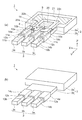
図1(a)は、本実施形態に係る水晶振動片の表面側から見た外観を示す斜視図であり、図1(b)は、水晶振動片の裏面側から見た外観を示す斜視図である。また、図2は、振動腕の表面側から見た構成を示す断面図を含む斜視図である。本実施形態の水晶振動片(屈曲振動片)1においては、図1(a)に示すように、基部2の主部2aと薄部2bとが同一面である側を表面側とし、図1(b)に示すように、基部2の主部2aと薄部2bとが段差をなす側を裏面側として、表裏方向を厚さとする。
FIG. 1A is a perspective view showing an appearance viewed from the front surface side of the quartz crystal resonator element according to the present embodiment, and FIG. 1B is a perspective view showing an appearance viewed from the back surface side of the crystal oscillator piece. It is. FIG. 2 is a perspective view including a cross-sectional view showing a configuration viewed from the surface side of the vibrating arm. In the crystal vibrating piece (flexural vibrating piece) 1 of the present embodiment, as shown in FIG. 1A, the side where the
この水晶振動片1は、屈曲基板として、基部2と、3本の振動腕3(3a,3b,3c)と、を備えている。基部2は、直方体状の主部2aと、主部2aの長手辺側から長手辺の長さより短幅で延長して形成され、表面側が主部2aと同一面であり、裏面側が主部2aと段差をなし、その段差分だけ厚みの薄い直方体状の薄部2bと、を有している。また、振動腕3a,3b,3cのそれぞれは、薄部2bから主部2aと反対方向へ延長して形成され、薄部2bと同じ厚みを有し、基部2の長手方向に沿って等間隔に配置されている。
The
これら振動腕3a,3b,3cについて、図2に詳細な断面が示されている振動腕3cを代表にして説明する。振動腕3cは、直方体柱の形状であって、直方体柱の薄部2bの側には、振動腕3cの全周を取り巻いて酸化物誘電体である緩和層12(12c)が形成されている。この場合、緩和層12cは、振動腕3cにおいて、薄部2bと反対方向の先端側の部分には形成されていない。さらに、緩和層12は、緩和層12cから連続して、薄部2bの表面側にも形成されていて、振動腕3bおよび振動腕3aの方向へ延在している。そして、振動腕3cの表面側に形成された緩和層12cには、金属膜の下部電極11(11c)が緩和層12cに重ねて形成されている。下部電極11cの薄部2bの側は、薄部2bの緩和層12に重ねて形成されている電極配線23cと電気的に導通した状態で接続している。電極配線23cは、緩和層12の主部2a側の辺に沿って延在し、振動腕3aの方向へ延びている。
The
また、振動腕3cには、振動腕3cの全周を取り巻き、下部電極11cの全領域を覆うように圧電膜14(14c)が形成されている。さらに、圧電膜14は、圧電膜14cから連続して、薄部2bの緩和層12の領域および電極配線23cを覆うようにも形成され、緩和層12cの全領域を覆っている。そして、振動腕3cに形成された圧電膜14cの表面側には、金属膜の上部電極10(10c)が形成されていて、この構成によれば、圧電膜14cは、下部電極11cと上部電極10cとで挟持されている状態である。
In addition, a piezoelectric film 14 (14c) is formed on the vibrating
そして、図1に示すように、振動腕3aは、振動腕3cと同様な構成であって、振動腕3aの全周を取り巻いて形成された緩和層12aと、緩和層12aの表面側に重ねて形成された金属膜の下部電極11aと、緩和層12aおよび下部電極11aの全領域を覆い、振動腕3aの全周を取り巻くように形成された圧電膜14aと、圧電膜14aの表面側に形成された金属膜である上部電極10aと、を有している。同様に、振動腕3bは、緩和層12b、下部電極11b、圧電膜14b、上部電極10bを有している。下部電極11aと下部電極11bとには、図4で後述する電極配線23aと電極配線23bとがそれぞれ接続されている。
As shown in FIG. 1, the resonating
なお、この場合、水晶振動片1において、圧電膜14としては、反応性スパッタリングで0.1〜0.5μm程度の厚さに形成した窒化アルミニウム(AlN)を用いている。窒化アルミニウム(AlN)は、膜形成時において、極性が反転しにくい特性を有し、配向性の揃った膜形成が可能であるため、優れた圧電効果を示すものである。また、緩和層12としては、スパッタリングで形成した酸化アルミニウム(Al2O3、アルミナ)を用いていて、酸化アルミニウム(Al2O3)は、基部2および振動腕3を形成する水晶と酸素拡散により強固に結合し、圧電膜14とアルミニウム拡散により強固に結合する。さらに、緩和層12の酸化アルミニウム(Al2O3)は、線膨張係数が7.1ppm/℃であり、線膨張係数が13.7ppm/℃である水晶と、線膨張係数が5.27ppm/℃である窒化アルミニウム(AlN)との中間値である。そのため、水晶へ窒化アルミニウム(AlN)を直接形成する場合に比べて、熱が作用しても、線膨張係数の違いによる境界面での残留応力や歪に起因する位置ズレ等を緩和できる。従って、水晶振動片1は、緩和層12を有することにより、水晶で形成された基部2および振動腕3と、圧電膜14と、の密着性を間接的ながら良好に保持することが可能である。
In this case, in the
また、下部電極11および電極配線23a,23b,23cは、フォトリソグラフィーおよびエッチングにより形成され、緩和層12の側の下層膜であるチタン(Ti)および圧電膜14の側の上層膜であるプラチナ(Pt)の2層構成の金属膜である。これら2層構成の金属膜は、合計0.1μm程度の厚さに形成されている。このように、下部電極11の下層膜としてチタン(Ti)を用いれば、水晶との密着性が良好であり、下部電極11の上層膜としてプラチナ(Pt)を用いれば、窒化アルミニウム(AlN)の配向性を揃える効果を促しやすい効果がある。尚、プラチナ以外に窒化アルミニウムの配向性を促す可能性のある金属膜としては、Au、Al、Ag、Cu、Mo、Cr、Nb、W、Ni、Fe、Ti、Co、Zn、Zr、などがある。そして、上部電極10および電極配線22a,22b,22cは、フォトリソグラフィーおよびエッチングにより形成され、圧電膜14の側の下層膜であるクロム(Cr)および上層膜である金(Au)の2層構成の金属膜である。これら2層構成の金属膜は、合計0.1μm程度の厚さに形成されている。
The
ここで、緩和層12、下部電極11および電極配線23について、特に電極配線の詳細を説明する。図4は、緩和層、下部電極および電極配線の構成を示す斜視図である。図4に示すように、緩和層12は、緩和層12a,12b,12cのように、振動腕3a,3b,3cの薄部2b側の全周をそれぞれ取り巻く領域と、薄部2bの表面側の領域と、に形成されている。下部電極11は、下部電極11a,11b,11cのように、緩和層12a,12b,12cにそれぞれ形成されている。電極配線23は、振動腕3aの下部電極11aから基部2の方向へ延長して形成された電極配線23aと、振動腕3bの下部電極11bから基部2の方向へ延長して形成された電極配線23bと、既述した電極配線23cと、から成る。電極配線23aは、下部電極11aから緩和層12の主部2a側の辺へ向かって延長し、さらに主部2a側の辺に沿って延伸して、電極配線23cと接続している。つまり、電極配線23aと電極配線23cとは、U字の形状をなしている。そして、電極配線23bは、薄部2bの緩和層12に形成され、このU字の内側に位置し、下部電極11bから基部2および振動腕3aに向かって延在している。
Here, with respect to the
また、これら緩和層12、下部電極11および電極配線23を覆って、水晶振動片1には、圧電膜が形成されており、図5は、圧電膜の構成を示す斜視図である。図5に示すように、圧電膜14は、緩和層12の全領域を覆っていて、緩和層12との間に、下部電極11および電極配線23を挟持している。また、圧電膜14は、薄部2bの位置にある圧電膜14を貫通して設けられている導通孔4および導通孔5を有している。導通孔4は、圧電膜14を介して、電極配線23b(図4)と対向する位置にある。導通孔5は、圧電膜14を介して、U字の形状をなす電極配線23aおよび電極配線23c(図4)と対向する位置にある。
Further, a piezoelectric film is formed on the
図1に戻って、水晶振動片1は、その表面側に、振動腕3aの圧電膜14aを介して、下部電極11aと対向する位置に形成された金属膜の上部電極10aと、振動腕3bの圧電膜14bを介して、下部電極11bと対向する位置に形成された金属膜の上部電極10bと、同様に、振動腕3cの圧電膜14cを介して、下部電極11cと対向する位置に形成された金属膜の上部電極10cと、を有している。また、水晶振動片1は、振動腕3aの上部電極10aから延長し基部2の薄部2bおよび主部2aの外縁に沿って形成された電極配線22aと、振動腕3cの上部電極10cから延長し基部2の薄部2bおよび主部2aの外縁に沿って形成された電極配線22cと、電極配線22aと電極配線22cとに接続して形成された電極端子21と、を有している。電極配線22aおよび電極配線22cは、緩和層12と基部2とに渡ってそれぞれの表面側に連続して形成され、電極端子21は、基部2の表面側に形成されている。これら電極配線22a、電極端子21および電極配線22cは、U字の形状をなして延在している。さらに、水晶振動片1は、このU字の形状の内側にあり、基部2の表面側に形成された電極端子20と、振動腕3bの上部電極10bから延長して形成され電極端子20へ接続された電極配線22bと、を有している。
Returning to FIG. 1, the quartz
そして、電極配線22aは、導通孔4の方向へ延在し、導通孔4の内壁にも金属膜が形成されている。これにより、電極配線22aと、電極配線23bと、が接続され、即ち、電極端子21と、上部電極10a,10cおよび下部電極11bと、が電気的に接続された状態になる。同様に、電極配線22bは、導通孔5の方向へ延在し、導通孔5の内壁にも金属膜が形成されている。これにより、電極配線22bと、電極配線23aおよび電極配線23cと、が接続され、即ち、電極端子20と、上部電極10bおよび下部電極11a,11cと、が電気的に接続された状態になる。このような構成である水晶振動片1は、電極端子20,21へ電流が印加されると、振動腕3が水晶振動片1の表面側または裏面側へ交互に屈曲する構成である。
The
次に、水晶振動片1の屈曲について説明する。図3は、水晶振動片の屈曲原理を説明するための模式図である。図3に示すように、水晶振動片1は、振動腕3aにおいて、電極端子21と上部電極10aとが電極配線22aによって接続し、下部電極11aと電極端子20とが電極配線23aおよび導通孔5によって接続している。また、振動腕3cにおいて、電極端子21と上部電極10cとが電極配線22cによって接続し、下部電極11cと電極端子20とが電極配線23cおよび導通孔5によって接続している。つまり、振動腕3aおよび振動腕3cは、共に同方向の駆動電流が印加される。一方、振動腕3bにおいては、電極端子21と下部電極11bとが電極配線23bおよび導通孔4によって接続し、上部電極10bと電極端子20とが電極配線22bによって接続している。つまり、振動腕3bには、振動腕3aおよび振動腕3cと異なる方向の駆動電流が印加されるようになっている。
Next, the bending of the
例えば、振動腕3aの圧電膜14aは、電極端子20,21へ駆動電流が印加されると、発生する電界による電界効果によって、この場合、圧縮する。この圧縮により、振動腕3aは、表面側の方向へ屈曲する。同様に、振動腕3cも表面側の方向へ屈曲する。一方、振動腕3bの圧電膜14bは、振動腕3a,3bとは反対方向の駆動電流が印加されるため、振動腕3a,3bとは反対方向の向きに発生する電界による電界効果によって伸張する。この伸張により、振動腕3bは、裏面側の方向へ屈曲する。即ち、隣り合って位置する振動腕3は、互いに逆の位相で屈曲し、いわゆる面外振動をする。そして、電極端子20および電極端子21へ印加する駆動電流の方向を変えると、振動腕3は、それぞれ逆方向へ屈曲する。つまり、印加する駆動電流の方向を交互に変えることにより、水晶振動片1は、振動腕3が屈曲を繰り返し、安定した振動をすることが可能である。
For example, when a drive current is applied to the
次に、屈曲振動片としての水晶振動片1を構成する各部の仕様について、製造方法と共に説明する。まず、水晶振動片1の基部2および振動腕3は、圧電単結晶材である水晶柱から切り出される。水晶柱は、六角柱であって、柱の長手方向に光軸であるZ軸と、Z軸に垂直な六角形面のX−Y平面において、六角形の辺に平行な電気軸であるX軸と、X軸に垂直な機械軸であるY軸とを有している。このような水晶は、X軸(電気軸)方向に電圧を加えると、加えた電圧の方向に対応してY軸(機械軸)方向に伸びあるいは縮みの現象が生じ、逆に、Y軸(機械軸)方向に引っ張りあるいは圧縮を与えると、X軸(電気軸)方向に電圧が生じる性質を有している。つまり、水晶は、電気的エネルギーと機械的エネルギーとの変換が可能である。水晶のこの性質を有効に利用するため、水晶振動片1の基部2および振動腕3は、水晶柱のX−Y平面において、X軸回りに約1〜5度傾けたX−Y’平面に沿って切り出された水晶ウエハー(不図示)から、さらにバッファード弗酸(BHF)を用いた異方性エッチング等により所定の薄板状に切り出されたものであり、表裏の方向であるZ’方向に厚さを有している。この場合、基部2における主部2aの厚さが50μm、そして、振動腕3の厚さが10μmに形成されている。このように切り出された振動腕3は、厚さ方向に安定して振動する特性を有している。
Next, the specification of each part which comprises the
次に、基部2および振動腕3を形成する水晶へ、緩和層12と下部電極11および電極配線23とを形成する。最初に、基部2および振動腕3の全面へ、スパッタリングにより、緩和層12としての酸化アルミニウム(Al2O3)を成膜し、酸化アルミニウム(Al2O3)に重ねて、下部電極11となるチタン(Ti)およびプラチナ(Pt)の2層からなる金属膜をスパッタリングにて成膜する。このプラチナ(Pt)の全面にレジスト剤を塗布し、レジスト剤の塗布後、フォトリソグラフィーを用いて、下部電極11および電極配線23となるべき部分にのみレジスト剤を残す。そして、エッチング処理(この場合王水処理)により、レジスト剤が残っている部分以外のチタン(Ti)およびプラチナ(Pt)の成膜を除去する。最後に、残っているレジスト剤を除去すれば、下部電極11および電極配線23の形状が形成される。なお、緩和層12となる酸化アルミニウム(Al2O3)は、まだ水晶の全面を覆った状態である。
Next, the
次に、緩和層12と下部電極11と電極配線23との全面を覆って、圧電膜14としての窒化アルミニウム(AlN)を反応性スパッタリングにより成膜する。この時、窒化アルミニウム(AlN)は、その柱状結晶がプラチナ(Pt)の膜面に対してほぼ垂直な方向へ成長し、配向性の揃った圧電膜となる。即ち、プラチナ(Pt)は、窒化アルミニウム(AlN)の配向性を揃える効果を促しやすい特性を有している。そして、下部電極11等の形状を形成した場合と同様に、圧電膜14および緩和層12の形状を形成するために、窒化アルミニウム(AlN)へレジスト剤をパターニングする。パターニングは、図4および図5に示すように、圧電膜14と緩和層12とが、振動腕3における基部2の側の周囲および薄部2bの上面側に残るようになされ、レジスト剤の無い部分の窒化アルミニウム(AlN)および酸化アルミニウム(Al2O3)が除去される。窒化アルミニウム(AlN)および酸化アルミニウム(Al2O3)の除去は、強アルカリ水溶液若しくは燐酸を用いて行い、この場合、燐酸を用いた。なお、圧電膜14には、導通孔4,5も同時に形成される。このようにして、圧電膜14および緩和層12が形成される。
Next, aluminum nitride (AlN) as the
最後に、上部電極10、電極端子20,21および電極配線22となる金属膜を、下部電極11および電極配線23と同様な方法で、圧電膜14へ形成する。上部電極10、電極端子20,21および電極配線22は、圧電膜14の側の下層膜であるクロム(Cr)および上層膜である金(Au)の2層からなる金属膜である。このようにして、水晶振動片1が完成する。
Finally, a metal film that becomes the
以下、実施形態における水晶振動片1の主効果を記載する。
Hereinafter, the main effects of the
(1)水晶振動片1は、基部2および振動腕3を形成している水晶と、圧電膜14と、の間に、緩和層12が直接形成されている。この緩和層12は、酸化アルミニウム(Al2O3)であって、水晶を構成している酸素元素および圧電膜14の窒化アルミニウム(AlN)を構成しているアルミニウム元素を含んでおり、水晶と酸素拡散により強固に結合し、圧電膜14とアルミニウム拡散により強固に結合することができる組成となっている。これにより、振動腕3と圧電膜14との密着性が間接的に高められ、振動腕3は、圧電膜14の圧電効果によって、確実に屈曲振動が行える。
(1) In the
(2)緩和層12は、その線膨張係数が、水晶および圧電膜14に比べて、水晶より小さく、圧電膜14より大きな中間値である。これにより、緩和層12および圧電膜14の形成時に、熱が作用しても、線膨張係数の違いによる境界面での残留応力や歪による位置ズレ等が緩和され、圧電膜14は、緩和層12を介して、水晶との密着性が良好に保持される。
(2) The
(3)水晶振動片1は、振動腕3の全周に緩和層12および圧電膜14が形成されている。そのため、仮に、表面側の圧電膜14に残留応力等があっても、裏面側の圧電膜14によって打ち消され、振動腕3の屈曲へ影響を与えない構成である。
(3) In the
また、屈曲振動片は上記の実施形態に限定されるものではなく、次に挙げる変形例のような形態であっても、実施形態と同様な効果が得られる。 In addition, the bending vibration piece is not limited to the above-described embodiment, and the same effects as those of the embodiment can be obtained even in a form such as the following modification.
(変形例1)水晶振動片1の緩和層12は、スパッタリングで形成した酸化アルミニウム(Al2O3)であるが、これに限定されるものではなく、例えば、酸化物誘電体であって、酸化アルミニウム(Al2O3)の線膨張係数7.1ppm/℃に近似の線膨張係数を有する酸化チタニウム(TiO2、線膨張係数9ppm/℃)、二酸化珪素(SiO2、線膨張係数6ppm/℃)、酸化ジルコニウム(ZrO2、線膨張係数9.2ppm/℃)等であっても良い。
(Modification 1) The
(変形例2)緩和層12は、振動腕3と、圧電膜14および下部電極11および電極配線22と、の間に形成されているが、下部電極11および電極配線22と、振動腕3と、の間には、形成されていない構成であっても良い。または、緩和層12が基部2および振動腕3の全面に形成されている構成であっても良い。このような形態の水晶振動片も、水晶振動片1と同様な効果を奏する。
(Modification 2) The
(変形例3)水晶振動片1は、3本の振動腕3a,3b,3cを備えて、いわゆる面外振動をするが、これに限定されるものではなく、3本以外の振動腕3を備える形態の振動片であっても良く、さらに、面外振動ではなく、振動腕がその振動方向に沿って配置される面内振動をする形態のものであっても良い。
(Modification 3) The quartz
(変形例4)水晶振動片1の下部電極11は、チタン(Ti)およびプラチナ(Pt)の2層構造の金属膜であるが、窒化アルミニウム(AlN)の配向性を促すものであれば、これに限定されることなく、モリブデン(Mo)やチタン(Ti)等の単層構造の金属膜等であっても良い。
(Modification 4) The
(変形例5)水晶振動片1の圧電膜14は、反応性スパッタリングにより形成された窒化アルミニウム(AlN)であるが、これに限定されるものではなく、例えば、圧電性を有する酸化亜鉛(ZnO)等であっても良い。
(Modification 5) The
(変形例6)屈曲振動片は、水晶振動片1のような水晶を用いたものに限定されることなく、ニオブ酸リチウム(LiNbO3)、チタン酸ジルコン鉛(PZT)等の他の圧電性材料であっても良い。更に、屈曲振動片は圧電性材料に限定されるものではなく、シリコンやゲルマニウムなどの非圧電材料であっても良い。本発明による屈曲振動片は、圧電薄膜に電界を加えることにより屈曲振動片を振動させるものであり、屈曲振動片に圧電性能は必要ないからである。このように振動腕3がシリコンの場合、緩和層12として二酸化珪素(SiO2)を用い、圧電膜14として酸化亜鉛(ZnO)を用いることが好ましい。
(Modification 6) The flexural vibration piece is not limited to the one using the quartz crystal such as the
(変形例7)水晶振動片1は、表面側にのみ上部電極10および下部電極11を有している構成であるが、この電極構成に限定されるものではなく、裏面側にも上部電極および下部電極を有している構成であっても良い。図6(a)は、水晶振動片の変形例を示す断面図であり、図6(b)は、水晶振動片の変形例における屈曲原理を示す模式図である。図6(a)に示す水晶振動片100は、振動腕3のうちの1本を示していて、水晶振動片1と同一の構成部分については、同一符号を付してある。水晶振動片100は、水晶振動片1の構成に加え、裏面側の緩和層12と圧電膜14との間に、下部電極15を有している。下部電極15は、振動腕3を介して表面側の下部電極11と対向する位置に配置されている。そして、下部電極15との間に圧電膜14を挟持して上部電極16が配置されている。また、図6(b)に示すように、振動腕3aの下部電極11aと下部電極15aとは、電気的に接続されていて、同様に、振動腕3bの下部電極11bと下部電極15b、および振動腕3cの下部電極11cと下部電極15cとは、それぞれ接続されている。
(Modification 7) The quartz
ここで、振動腕3(3a,3b,3c)の表面側に形成されている圧電膜14(14a,14b,14c)は、例えば、無負荷状態に於いて圧電膜中の自発分極が図中の上向きであるような分極方向P1を有している。一方、振動腕3の裏面側に形成されている圧電膜14は、無負荷状態での圧電膜中の自発分極が図中の下向きである分極方向P2であって、分極方向P1と反対の分極方向を有している。即ち、振動腕3の表面側と裏面側との圧電膜14は、それぞれ互いに反対の分極方向を有している。
Here, in the piezoelectric film 14 (14a, 14b, 14c) formed on the surface side of the vibrating arm 3 (3a, 3b, 3c), for example, spontaneous polarization in the piezoelectric film is illustrated in an unloaded state. The polarization direction P1 is upward. On the other hand, the
そして、水晶振動片100には、電極端子20または電極端子21から駆動電圧が印加される。例えば、電極端子21から電極端子20へ駆動電流が印加されると、駆動電流は、振動腕3aにおいて、表面側の上部電極10aから表面側の圧電膜14a、下部電極11a、裏面側の下部電極15a、圧電膜14a、上部電極16aを直列接続した状態で、電極端子20へ順に至る。同様に、駆動電流は、振動腕3cにおいて、電極端子21から表面側の上部電極10c、圧電膜14c、下部電極11c、裏面側の下部電極15c、圧電膜14c、上部電極16cを直列接続した状態で、電極端子20へ至る。一方、振動腕3bにおいては、駆動電流が電極端子21から裏面側の上部電極16bへまず印加され、圧電膜14b、下部電極15b、表面側の下部電極11b、圧電膜14b、上部電極10bを直列接続した状態で、電極端子20へ至る。
A driving voltage is applied to the
従って、振動腕3aにおいては、表面側の圧電膜14aと裏面側の圧電膜14aとに、表面側から裏面側の方向へ、同方向の駆動電流が印加されるため、両方の圧電膜14aには、共に、表面側から裏面側の方向へ向いた電界が生じる。これにより、分極方向P1と電界とが反対の方向である表面側の圧電膜14aは、電界による電界効果によって伸張し、分極方向P2と電界とが同一の方向である裏面側の圧電膜14aは、電界による電界効果によって圧縮する。この伸張および圧縮により、振動腕3aは、裏面側の方向へ屈曲する。同様に、振動腕3cも裏面側の方向へ屈曲する。一方、振動腕3bにおいては、表面側の圧電膜14bと裏面側の圧電膜14bとに、裏面側から表面側の方向へ、同方向の駆動電流が印加されるため、両方の圧電膜14bには、共に、裏面側から表面側の方向へ向いた電界が生じる。これにより、分極方向P1と電界とが同一の方向である表面側の圧電膜14bは、電界による電界効果によって圧縮し、分極方向P2と電界とが反対の方向である裏面側の圧電膜14bは、電界による電界効果によって伸張する。この圧縮および伸張により、振動腕3bは、表面側の方向へ屈曲する。即ち、隣り合って位置する振動腕3は、互いに逆の位相で屈曲し、いわゆる面外振動をする。電極端子20および電極端子21へ印加する駆動電流の方向を変えると、振動腕3は、それぞれ逆方向へ屈曲する。つまり、印加する駆動電流の方向を交互に変えることにより、水晶振動片100は、振動腕3が屈曲を繰り返して振動する。このように、裏面側にも上部電極16と下部電極15とを有する水晶振動片100は、より安定した振動をすることができる。
Accordingly, in the vibrating
(変形例8)水晶振動片1は、表面側および裏面側の両側に、緩和層12と圧電膜14とを有する構成であるが、この電極構成に限定されず、上部電極10および下部電極11が形成されている表面側にのみ、緩和層12と圧電膜14とを形成した構成であっても良い。この構成であっても、水晶振動片は、ほぼ同様な面外振動をすることができる。
(Modification 8) The quartz
屈曲振動片としての水晶振動片1は、緩和層12を設けることにより、振動腕3と圧電膜14とが、緩和層12を介して、良好な密着性を有することになるため、安定した正確な振動をすることができる。この特徴により、水晶振動片1は、タイミングデバイス等として、デジタル携帯電話、パーソナルコンピューター、電子時計、ビデオレコーダー、テレビなどの電子機器に広く用いられる。そして、この水晶振動片1をパッケージ化した水晶振動子や、水晶振動片1と水晶振動片1を駆動させるための半導体素子とを備えた屈曲振動デバイス等も安定した正確な振動が可能であり、搭載される電子機器の品質向上に貢献することができる。
The quartz
1…屈曲振動片としての水晶振動片、2…基部、3…振動腕、4,5…導通孔、10…上部電極、11…下部電極、12…酸化物誘電体としての緩和層、14…圧電膜、15…下部電極、16…上部電極、20…電極端子、21…電極端子、22…電極配線、23…電極配線、100…水晶振動片。
DESCRIPTION OF
Claims (6)
少なくとも前記屈曲基板と前記圧電膜との間に緩和層をさらに備え、該緩和層は、前記屈曲基板または前記圧電膜のいずれかを構成する元素を一種以上含み、
前記緩和層の線膨張係数は、前記屈曲基板の線膨張係数と前記圧電膜の線膨張係数との中間値であることを特徴とする屈曲振動片。 A bent substrate having a base and a vibrating arm projecting from the base; a lower electrode formed on the vibrating arm; a piezoelectric film formed on the lower electrode; and an overlay on the piezoelectric film An upper electrode formed by the bending vibration piece,
Further comprising a relief layer at least between the bent substrate the piezoelectric film, the moderate sum layer, viewed contains one or more elements constituting one of the bent substrate or the piezoelectric film,
The bending vibration piece, wherein the relaxation layer has a linear expansion coefficient that is an intermediate value between a linear expansion coefficient of the bent substrate and a linear expansion coefficient of the piezoelectric film .
前記緩和層は、前記屈曲基板を構成する元素と前記圧電膜を構成する元素とをそれぞれ一種以上含むことを特徴とする屈曲振動片。 The bending vibration piece according to claim 1 ,
The bending vibration piece, wherein the relaxation layer includes at least one element constituting the bent substrate and one element constituting the piezoelectric film.
前記屈曲基板は、水晶であることを特徴とする屈曲振動片。 The bending vibration piece according to claim 1 or 2 ,
The bending vibration piece, wherein the bending substrate is a crystal.
前記圧電膜は、窒化アルミニウムまたは酸化亜鉛であることを特徴とする屈曲振動片。 In the bending vibration piece according to any one of claims 1 to 3 ,
The bending vibration piece, wherein the piezoelectric film is aluminum nitride or zinc oxide.
前記緩和層は、酸素原子を含む酸化物誘電体であることを特徴とする屈曲振動片。 In the bending vibration piece according to any one of claims 1 to 4 ,
The bending vibration piece, wherein the relaxation layer is an oxide dielectric containing oxygen atoms.
前記緩和層は、酸化チタニウム、二酸化珪素、酸化アルミニウムのいずれかであることを特徴とする屈曲振動片。 The bending vibration piece according to claim 5 ,
The bending vibration piece, wherein the relaxation layer is any one of titanium oxide, silicon dioxide, and aluminum oxide.
Priority Applications (1)
| Application Number | Priority Date | Filing Date | Title |
|---|---|---|---|
| JP2009233068A JP5375503B2 (en) | 2009-10-07 | 2009-10-07 | Bending vibration piece |
Applications Claiming Priority (1)
| Application Number | Priority Date | Filing Date | Title |
|---|---|---|---|
| JP2009233068A JP5375503B2 (en) | 2009-10-07 | 2009-10-07 | Bending vibration piece |
Publications (3)
| Publication Number | Publication Date |
|---|---|
| JP2011082782A JP2011082782A (en) | 2011-04-21 |
| JP2011082782A5 JP2011082782A5 (en) | 2012-07-19 |
| JP5375503B2 true JP5375503B2 (en) | 2013-12-25 |
Family
ID=44076377
Family Applications (1)
| Application Number | Title | Priority Date | Filing Date |
|---|---|---|---|
| JP2009233068A Active JP5375503B2 (en) | 2009-10-07 | 2009-10-07 | Bending vibration piece |
Country Status (1)
| Country | Link |
|---|---|
| JP (1) | JP5375503B2 (en) |
Families Citing this family (7)
| Publication number | Priority date | Publication date | Assignee | Title |
|---|---|---|---|---|
| JP5369741B2 (en) * | 2009-02-12 | 2013-12-18 | セイコーエプソン株式会社 | Vibrating piece and vibrator |
| JP5685962B2 (en) | 2011-02-02 | 2015-03-18 | セイコーエプソン株式会社 | Vibrating piece, vibrator, oscillator and electronic device |
| US8581669B2 (en) | 2011-02-02 | 2013-11-12 | Seiko Epson Corporation | Vibrator element, vibrator, oscillator, and electronic apparatus |
| JP6482169B2 (en) | 2013-07-19 | 2019-03-13 | セイコーエプソン株式会社 | Vibrating piece, vibrator, oscillator, electronic device and moving object |
| JP2015046807A (en) * | 2013-08-29 | 2015-03-12 | セイコーエプソン株式会社 | Vibration piece, vibrator, oscillator, electronic apparatus and moving body |
| JP6331702B2 (en) * | 2014-05-29 | 2018-05-30 | セイコーエプソン株式会社 | Electronic devices, electronic devices, and moving objects |
| KR20210085954A (en) * | 2019-12-31 | 2021-07-08 | 엘지디스플레이 주식회사 | Flexible Vibration Film And Display Having The Same |
Family Cites Families (2)
| Publication number | Priority date | Publication date | Assignee | Title |
|---|---|---|---|---|
| JP2007183147A (en) * | 2006-01-06 | 2007-07-19 | Matsushita Electric Ind Co Ltd | Vibrating element and angular velocity sensor using the same |
| JP4533934B2 (en) * | 2008-01-15 | 2010-09-01 | エプソントヨコム株式会社 | Vibrating piece and method of manufacturing vibrator |
-
2009
- 2009-10-07 JP JP2009233068A patent/JP5375503B2/en active Active
Also Published As
| Publication number | Publication date |
|---|---|
| JP2011082782A (en) | 2011-04-21 |
Similar Documents
| Publication | Publication Date | Title |
|---|---|---|
| JP5375503B2 (en) | Bending vibration piece | |
| JP5622173B2 (en) | Vibrating piece, vibrator, oscillator, and electronic device | |
| JP2011004035A (en) | Flexural vibration piece, and method for manufacturing flexural vibration piece | |
| JP5593979B2 (en) | Vibrating piece, vibrator, oscillator, sensor and electronic equipment | |
| JP2010252302A (en) | Bending vibrator piece and oscillator using the same | |
| JP4636093B2 (en) | Vibrating piece, vibrator, oscillator, and vibrating piece manufacturing method | |
| JP2013062643A (en) | Vibration piece, vibrator, oscillator, and electronic apparatus | |
| JP2015041785A (en) | Vibration piece, vibrator, oscillator, electronic apparatus, and mobile | |
| JP2011228922A (en) | Vibrating reed, method for manufacturing the same, and vibrator and oscillator | |
| JP5685962B2 (en) | Vibrating piece, vibrator, oscillator and electronic device | |
| JP5347546B2 (en) | Vibrating piece, vibrating piece manufacturing method, and vibrator | |
| JP2012015886A (en) | Vibrating reed, vibrator, oscillator, and electronic apparatus | |
| JP5822186B2 (en) | Vibrators, oscillators, and electronics | |
| JP5434712B2 (en) | Piezoelectric vibrating piece and piezoelectric device | |
| JP2010103805A (en) | Bending vibration piece, bending vibrator, and piezoelectric device | |
| JP5531809B2 (en) | Bending vibrator, bending vibrator, oscillator and electronic equipment | |
| JP5923862B2 (en) | Vibrating piece, vibrator, oscillator and electronic device | |
| JP5533349B2 (en) | Bending vibrator, bending vibrator, oscillator, and electronic device | |
| JP6327327B2 (en) | Vibrator, electronic device, mobile object, and oscillator | |
| JP2012029024A (en) | Bending vibration piece, vibrator, oscillator, and electronic apparatus | |
| JP6064342B2 (en) | Vibrating piece and electronic equipment | |
| JP2012160995A (en) | Vibrator element, vibrator, oscillator, and electronic apparatus | |
| JP2012023526A (en) | Bending vibration piece, vibrator, oscillator, and electronic apparatus | |
| JP2012182610A (en) | Vibration piece, vibrator, oscillator and electronic apparatus | |
| JP2012147347A (en) | Vibration piece, vibrator, oscillator and electronic apparatus |
Legal Events
| Date | Code | Title | Description |
|---|---|---|---|
| A521 | Request for written amendment filed |
Free format text: JAPANESE INTERMEDIATE CODE: A523 Effective date: 20120605 |
|
| A621 | Written request for application examination |
Free format text: JAPANESE INTERMEDIATE CODE: A621 Effective date: 20120605 |
|
| A977 | Report on retrieval |
Free format text: JAPANESE INTERMEDIATE CODE: A971007 Effective date: 20130516 |
|
| A131 | Notification of reasons for refusal |
Free format text: JAPANESE INTERMEDIATE CODE: A131 Effective date: 20130528 |
|
| A521 | Request for written amendment filed |
Free format text: JAPANESE INTERMEDIATE CODE: A523 Effective date: 20130724 |
|
| RD03 | Notification of appointment of power of attorney |
Free format text: JAPANESE INTERMEDIATE CODE: A7423 Effective date: 20130724 |
|
| TRDD | Decision of grant or rejection written | ||
| A01 | Written decision to grant a patent or to grant a registration (utility model) |
Free format text: JAPANESE INTERMEDIATE CODE: A01 Effective date: 20130827 |
|
| A61 | First payment of annual fees (during grant procedure) |
Free format text: JAPANESE INTERMEDIATE CODE: A61 Effective date: 20130909 |
|
| R150 | Certificate of patent or registration of utility model |
Ref document number: 5375503 Country of ref document: JP Free format text: JAPANESE INTERMEDIATE CODE: R150 Free format text: JAPANESE INTERMEDIATE CODE: R150 |
|
| S531 | Written request for registration of change of domicile |
Free format text: JAPANESE INTERMEDIATE CODE: R313531 |
|
| R350 | Written notification of registration of transfer |
Free format text: JAPANESE INTERMEDIATE CODE: R350 |