JP5374860B2 - Microactuator and manufacturing method thereof, microactuator array, microactuator device, optical device, display device, exposure apparatus, and device manufacturing method - Google Patents
Microactuator and manufacturing method thereof, microactuator array, microactuator device, optical device, display device, exposure apparatus, and device manufacturing method Download PDFInfo
- Publication number
- JP5374860B2 JP5374860B2 JP2007290577A JP2007290577A JP5374860B2 JP 5374860 B2 JP5374860 B2 JP 5374860B2 JP 2007290577 A JP2007290577 A JP 2007290577A JP 2007290577 A JP2007290577 A JP 2007290577A JP 5374860 B2 JP5374860 B2 JP 5374860B2
- Authority
- JP
- Japan
- Prior art keywords
- plate
- microactuator
- electrode
- region
- optical device
- Prior art date
- Legal status (The legal status is an assumption and is not a legal conclusion. Google has not performed a legal analysis and makes no representation as to the accuracy of the status listed.)
- Active
Links
Images


Abstract
Description
本発明は、マイクロアクチュエータ、マイクロアクチュエータアレー、マイクロアクチュエータ装置、光学デバイス、表示装置、露光装置、及びデバイス製造方法に関するものである。 The present invention relates to a microactuator, a microactuator array, a microactuator device, an optical device, a display device, an exposure apparatus, and a device manufacturing method.
MEMS(Micro-Electro-Mechanical System)技術の進展に伴い、この技術を応用したマイクロアクチュエータや、これを利用したDMD(Digital Micro-mirror Device)等の光学デバイスや、このような光学デバイスを利用した投影表示装置やこのような光学デバイスを可変整形マスク(プログラマブルマスクやアクティブマスクとも呼ばれる。)として用いた露光装置などが、種々提案されている。 Along with the development of MEMS (Micro-Electro-Mechanical System) technology, microactuators using this technology, optical devices such as DMD (Digital Micro-mirror Device) using this technology, and such optical devices were used. Various projection apparatuses and exposure apparatuses using such optical devices as variable shaping masks (also called programmable masks or active masks) have been proposed.
例えば、下記特許文献1には、代表的なDMDが開示されている。このDMDでは、ミラーをトーションヒンジで保持し、静電力によりヒンジをねじれ変形させてミラーを回転させてその向きを変え、入射光の反射方向を変える。この基本単位を複数1次元状や2次元状に並べて空間光変調器とし、光学的情報処理装置、投影表示装置や静電写真印刷装置などに応用されている。
For example, the following
また、ミラーを設けた片持ち梁を静電力で撓ませて、入射光の反射方向を変える光学デバイスも、知られている。 An optical device that changes the reflection direction of incident light by bending a cantilever provided with a mirror with an electrostatic force is also known.
ところが、トーションヒンジを用いたマイクロアクチュエータでは、ミラーの保持がトーションヒンジによるために、トーションヒンジの結合部に加わるねじりストレスによって破損し易く、その寿命を長くすることが困難であった。また、片持ち梁を用いたマイクロアクチュエータでは、片持ち梁の固有振動数が低いために応答速度を速くすることができなかった。 However, in the microactuator using the torsion hinge, since the mirror is held by the torsion hinge, it is easily damaged by the torsional stress applied to the coupling portion of the torsion hinge, and it is difficult to extend its life. Also, in the microactuator using a cantilever, the response speed cannot be increased because the natural frequency of the cantilever is low.
そこで、下記特許文献2には、V字形の凹部を有する基板上に両端を固定して前記凹部を掛け渡すように設けた両持ち梁を用いたマイクロミラーデバイスが、提案されている。このデバイスでは、両持ち梁に光反射膜が形成されて、ミラーが両持ち梁と全体的に一体化されている。静電力を加えない状態では、両持ち梁(すなわち、ミラー)は平板状をなす一方、静電力を加えると、両持ち梁(すなわち、ミラー)が静電力によってV字形の凹部に沿ってV字形に変形し、入射光の反射方向を変える。
Therefore, in
このデバイスでは、両持ち梁が用いられているため、トーションヒンジを用いる場合に比べて破損が生じ難くなり長寿命化を図ることができるとともに、固有振動数を高くすることができ、応答速度を速くすることができる。
しかしながら、特許文献2に開示されているデバイスでは、ミラーが両持ち梁と一体化されているため、両持ち梁が静電力によってV字形に変形するときには、ミラーもV字形に変形してしまい、ミラーの反射面は向きの異なる2つの面(V字形の一方の面と他方の面)になってしまう。その結果、反射光の方向が入射光が入射する位置に応じて大きく異なってしまい、迷光等を引き起こし易く、迷光に対する吸光処理等が困難になる。
However, in the device disclosed in
このように、特許文献2に開示されているデバイスでは、長寿命化及び応答速度の高速化の点で大変優れているものの、被駆動体であるミラーが両持ち梁と一体化されているので、被駆動体であるミラーも変形してしまい、これに起因して不都合が生ずるのである。
Thus, although the device disclosed in
また、特許文献2に開示されているようなミラーデバイスで用いられるマイクロアクチュエータに限らず、他の種々の用途において用いられるマイクロアクチュエータにおいても、被駆動体自体を変形させずに被駆動体の向きのみを変更することが要請される場合がある。
Further, not only the microactuator used in the mirror device disclosed in
さらに、このようなマイクロアクチュエータでは、より駆動の高速化を図るためには、駆動する際の振動が減衰して静定するまでの時間(静定時間)が短いことが好ましい。 Further, in such a microactuator, in order to further increase the driving speed, it is preferable that the time (stabilization time) until the vibration during driving attenuates and settles is short.
本発明は、このような事情に鑑みてなされたもので、長寿命化及び応答速度の高速化を図ることができ、しかも被駆動体自体を変形させずに被駆動体の向きのみを変更することができ、更には静定時間を短縮して駆動をより高速化することができるマイクロアクチュエータを提供することを目的とする。また、本発明は、このようなマイクロアクチュエータを用いたマイクロアクチュエータアレー、マイクロアクチュエータ装置、光学デバイス、表示装置、露光装置、並びに、このような露光装置を用いたデバイス製造方法を提供することを目的とする。 The present invention has been made in view of such circumstances, and can achieve a long life and a high response speed, and can change only the direction of the driven body without deforming the driven body itself. It is another object of the present invention to provide a microactuator that can shorten the settling time and increase the driving speed. Another object of the present invention is to provide a microactuator array using such a microactuator, a microactuator device, an optical device, a display device, an exposure apparatus, and a device manufacturing method using such an exposure apparatus. And
前記課題を解決するため、本発明の第1の態様によるマイクロアクチュエータは、基体と、該基体に支持された板状部材と、駆動力付与手段とを備え、前記板状部材は、前記板状部材の周辺部における全周又はその一部に渡る所定箇所で前記基体に対して固定されて、前記板状部材における前記所定箇所以外の領域で撓み変形可能であり、前記所定箇所は、前記板状部材の前記周辺部において互いに対向する2箇所を含み、被駆動体が、前記板状部材の撓み変形可能な領域のうちの所定部位に局所的に機械的に接続され、前記駆動力付与手段は、信号に応じて、前記板状部材の前記撓み変形可能な領域が撓み変形をして前記板状部材の前記所定部位の傾きが変化するように、前記板状部材の少なくとも一部に駆動力を付与し得るものであり、前記基体における前記板状部材との対向領域が平坦化され、前記駆動力付与手段は、前記基体に設けられた1つ以上の第1の電極部と、前記板状部材に設けられ前記1つ以上の第1の電極部との間の電圧により前記1つ以上の第1の電極部との間に静電力を生じ得る1つ以上の第2の電極部とを、含むものである。
本発明の第2の態様によるマイクロアクチュエータは、前記第1の態様において、前記1つ以上の第1の電極部は、前記板状部材の一部と対向するとともに前記板状部材の残りの部分とは対向しないものである。
In order to solve the above-mentioned problem, a microactuator according to a first aspect of the present invention includes a base, a plate-like member supported by the base, and a driving force applying unit, and the plate-like member is the plate-like member. It is fixed to the base body at a predetermined location over the entire circumference or a part of the periphery of the member, and can be bent and deformed in a region other than the predetermined location in the plate-like member. The driven member is locally mechanically connected to a predetermined portion of the plate-like member in a region where the plate-like member can be bent and deformed, and includes the two portions facing each other in the peripheral portion of the plate-like member, Is driven on at least a part of the plate-like member so that the bending-deformable region of the plate-like member is deformed in accordance with a signal and the inclination of the predetermined portion of the plate-like member changes. Can give power, Region facing the said plate-like member in the serial base is flattened, the driving force providing means, one or more of the first electrode portion provided on the base body, the one provided on the plate-like member One or more second electrode portions that can generate an electrostatic force between the one or more first electrode portions due to a voltage between the first electrode portion and the first electrode portion .
The microactuator according to a second aspect of the present invention is the microactuator according to the first aspect, wherein the one or more first electrode portions are opposed to a part of the plate member and the remaining part of the plate member. Is not opposite.
本発明の第3の態様によるマイクロアクチュエータは、前記第1又は第2の態様において、前記基体は、前記対向領域にCMPにより平坦化された平坦化膜を有するものである。 The microactuator according to a third aspect of the present invention is the microactuator according to the first or second aspect, wherein the base has a planarizing film planarized by CMP in the facing region.
本発明の第4の態様によるマイクロアクチュエータは、前記第1乃至第3のいずれかの態様において、前記駆動力が付与されない状態において、前記板状部材と前記板状部材と前記基体における前記対向領域との間の空隙が0.3μm以下であるものである。 The microactuator according to a fourth aspect of the present invention is the micro-actuator according to any one of the first to third aspects, in the state where the driving force is not applied, the plate member, the plate member, and the opposing region in the base body. The gap between them is 0.3 μm or less.
本発明の第5の態様によるマイクロアクチュエータは、前記第1乃至第4のいずれかの態様において、前記被駆動体が主平面を有し、前記板状部材の主平面と前記被駆動体の主平面とが略平行であるものである。 The microactuator according to a fifth aspect of the present invention is the microactuator according to any one of the first to fourth aspects, wherein the driven body has a main plane, the main plane of the plate-like member and the main body of the driven body. The plane is substantially parallel.
本発明の第6の態様によるマイクロアクチュエータは、前記第1乃至第5のいずれかの態様において、前記板状部材の前記所定部位は、前記板状部材の重心から偏心した部位であるものである。 The microactuator according to a sixth aspect of the present invention is the microactuator according to any one of the first to fifth aspects, wherein the predetermined portion of the plate-like member is a portion eccentric from the center of gravity of the plate-like member. .
本発明の第7の態様によるマイクロアクチュエータは、基体と、該基体に支持された板状部材と、駆動力付与手段とを備え、前記板状部材は、前記板状部材の周辺部における全周又はその一部に渡る所定箇所で前記基体に対して固定されて、前記板状部材における前記所定箇所以外の領域で撓み変形可能であり、前記所定箇所は、前記板状部材の前記周辺部において互いに対向する2箇所を含み、被駆動体が、前記板状部材の撓み変形可能な領域のうちの所定部位に局所的に機械的に接続され、前記駆動力付与手段は、信号に応じて、前記板状部材の前記撓み変形可能な領域が撓み変形をして前記板状部材の前記所定部位の傾きが変化するように、前記板状部材の少なくとも一部に駆動力を付与し得るものであり、前記基体における前記板状部材との対向領域が平坦化され、前記板状部材の前記所定部位は、前記板状部材の重心から偏心した部位であるものである。A microactuator according to a seventh aspect of the present invention includes a base, a plate-like member supported by the base, and a driving force imparting unit, and the plate-like member has an entire circumference in a peripheral portion of the plate-like member. Alternatively, it is fixed to the base at a predetermined position over a part thereof, and can be bent and deformed in an area other than the predetermined position in the plate-shaped member, and the predetermined position is in the peripheral portion of the plate-shaped member The driven body is locally mechanically connected to a predetermined part of the plate-shaped member in a region where the plate-like member can be bent and deformed. A driving force can be applied to at least a part of the plate-like member so that the bending-deformable region of the plate-like member is deformed to change the inclination of the predetermined portion of the plate-like member. Yes, the plate shape in the substrate Region facing the wood is flattened, the predetermined portion of the plate-shaped member is one that is part eccentric from the center of gravity of the plate-like member.
本発明の第8の態様によるマイクロアクチュエータアレーは、複数のマイクロアクチュエータと、複数の端子からなる第1の端子群と、複数の端子からなる第2の端子群と、を備えたマイクロアクチュエータアレーであって、(i)前記各マイクロアクチュエータは、前記第1乃至第6のいずれかの態様によるマイクロアクチュエータであり、(ii)前記各マイクロアクチュエータに関して、当該マイクロアクチュエータの前記第1の電極部が、前記第1及び第2の端子群のうちの一方の端子群のいずれか1つの端子に電気的に接続されるとともに前記第1及び第2の端子群の他の端子に電気的に接続されず、(iii)前記各マイクロアクチュエータに関して、当該マイクロアクチュエータの前記第2の電極部が、前記第1及び第2の端子群のうちの他方の端子群のいずれか1つの端子に電気的に接続されるとともに前記第1及び第2の端子群の他の端子に電気的に接続されず、(iv)前記各マイクロアクチュエータに関して、当該マイクロアクチュエータの前記第1の電極部に電気的に接続された第1又は第2の端子群の1つの端子と当該マイクロアクチュエータの前記第2の電極部に電気的に接続された前記第1又は第2の端子群の1つの端子との組み合わせは、当該マイクロアクチュエータに固有のものとなり、(v)前記第1の端子群の少なくとも1つの端子が、前記複数のマイクロアクチュエータのうちの2つ以上のマイクロアクチュエータの前記第1又は第2の電極部に、共通して電気的に接続され、(vi)前記第2の端子群の少なくとも1つの端子が、前記複数のマイクロアクチュエータのうちの2つ以上のマイクロアクチュエータの前記第1又は第2の電極部に、共通して電気的に接続されたものである。 A microactuator array according to an eighth aspect of the present invention is a microactuator array including a plurality of microactuators, a first terminal group including a plurality of terminals, and a second terminal group including a plurality of terminals. (I) each microactuator is a microactuator according to any one of the first to sixth aspects, and (ii) for each microactuator, the first electrode portion of the microactuator includes: It is electrically connected to one terminal of one of the first and second terminal groups and is not electrically connected to the other terminals of the first and second terminal groups. (Iii) For each microactuator, the second electrode portion of the microactuator is connected to the first and second terminal groups. And is not electrically connected to the other terminals of the first and second terminal groups, and (iv) for each microactuator, One terminal of the first or second terminal group electrically connected to the first electrode portion of the microactuator and the first or second electrically connected to the second electrode portion of the microactuator. The combination with one terminal of the second terminal group is unique to the microactuator, and (v) at least one terminal of the first terminal group is two or more of the plurality of microactuators. And (vi) at least one terminal of the second terminal group is connected to the plurality of micro-actuators. Commonly electrically connected to the first or second electrode section of two or more microactuators of the actuator.
前記(iv)の「固有」とは、第1の端子群から任意の1つの端子を選択するとともに第2の端子群から任意の1つの端子を選択したとき、この2つの端子に対応する(すなわち、この2つの端子が両電極にそれぞれ電気的に接続されている)マイクロアクチュエータが1つだけ特定される意味である。 The “unique” in (iv) corresponds to two terminals when any one terminal is selected from the first terminal group and any one terminal is selected from the second terminal group ( In other words, this means that only one microactuator (with these two terminals electrically connected to both electrodes) is specified.
本発明の第9の態様による光学デバイスは、前記第1乃至第7のいずれかの態様によるマイクロアクチュエータと、前記被駆動体とを備え、前記被駆動体が光学素子であるものである。 An optical device according to a ninth aspect of the present invention includes the microactuator according to any one of the first to seventh aspects and the driven body, and the driven body is an optical element.
本発明の第10の態様による光学デバイスは、前記第9の態様において、前記光学素子がミラーであるものである。 An optical device according to a tenth aspect of the present invention is the optical device according to the ninth aspect, wherein the optical element is a mirror.
本発明の第11の態様による光学デバイスは、前記第9又は第10の態様において、前記マイクロアクチュエータ及び前記光学素子の組を複数備えたものである。 An optical device according to an eleventh aspect of the present invention is the optical device according to the ninth or tenth aspect, comprising a plurality of sets of the microactuator and the optical element.
本発明の第12の態様による表示装置は、 空間光変調器を備えた表示装置であって、前記空間光変調器が前記第11の態様による光学デバイスであるものである。 A display device according to a twelfth aspect of the present invention is a display device including a spatial light modulator, wherein the spatial light modulator is an optical device according to the eleventh aspect.
本発明の第13の態様による露光装置は、照明光を用いて、物体を露光する露光装置であって、前記照明光の光路上に配置される前記第11の態様による光学デバイスを備え、該光学デバイスを介した前記照明光を用いて前記物体を露光するものである。 An exposure apparatus according to a thirteenth aspect of the present invention is an exposure apparatus that exposes an object using illumination light, comprising the optical device according to the eleventh aspect disposed on an optical path of the illumination light, The object is exposed using the illumination light via an optical device.
本発明の第14の態様による露光装置は、前記第13の態様において、前記光学デバイスは、前記照明光の照射により所定のパターンを生成するものである。 In an exposure apparatus according to a fourteenth aspect of the present invention, in the thirteenth aspect, the optical device generates a predetermined pattern by irradiation with the illumination light.
本発明の第15の態様による露光装置は、前記第13又は第14の態様において、前記物体を保持して移動する移動体を更に備え、前記光学デバイスの前記各マイクロアクチュエータの前記駆動力付与手段は、前記移動体の所定方向への移動に同期して制御されるものである。 The exposure apparatus according to a fifteenth aspect of the present invention is the exposure apparatus according to the thirteenth or fourteenth aspect, further comprising a moving body that holds and moves the object, and the driving force applying means for each microactuator of the optical device. Is controlled in synchronization with the movement of the moving body in a predetermined direction.
本発明の第16の態様によるデバイス製造方法は、リソグラフィ工程を含むデバイス製造方法であって、前記リソグラフィ工程では、前記第13乃至第15のいずれかの態様による露光装置を用いて露光を行うものである。
本発明の第17の態様によるデバイス製造方法は、基板と絶縁膜と固定電極と配線パターンとを含んで構成される基体と、前記基体に支持され、前記固定電極により撓み変形が可能な板状部材とを有するマイクロアクチュエータの製造方法であって、前記基板上に前記絶縁膜を成膜することと、前記固定電極が前記板状部材の一部と対向するとともに前記板状部材の残りの部分とは対向しないように、前記絶縁膜上に前記固定電極及び配線パターンを形成することと、前記絶縁膜上と、前記固定電極及び配線パターン上における、前記板状部材との対向領域に平坦化膜となるべき膜を成膜することと、前記平坦化膜となるべき膜を平坦化して平坦化膜とすることと、前記平坦化膜上に犠牲層を形成することと、前記犠牲層上に前記板状部材を形成することと、を含み、前記マイクロアクチュエータは前記第1乃至第7のいずれかの態様によるマイクロアクチュエータであるものである。
A device manufacturing method according to a sixteenth aspect of the present invention is a device manufacturing method including a lithography process, in which the exposure is performed using the exposure apparatus according to any one of the thirteenth to fifteenth aspects. It is.
According to a seventeenth aspect of the present invention, there is provided a device manufacturing method comprising: a base including a substrate, an insulating film, a fixed electrode, and a wiring pattern; and a plate-like shape supported by the base and capable of being bent and deformed by the fixed electrode. A method of manufacturing a microactuator having a member, wherein the insulating film is formed on the substrate, and the fixed electrode is opposed to a part of the plate member and the remaining part of the plate member Forming the fixed electrode and the wiring pattern on the insulating film so as not to face each other, and flattening on the insulating film and the region facing the plate-like member on the fixed electrode and the wiring pattern Forming a film to be a film, flattening the film to be the planarization film to form a planarization film, forming a sacrificial layer on the planarization film, and on the sacrificial layer The plate member Viewed including the method comprising forming the said microactuator is intended a microactuator according to the first to seventh either aspect.
本発明によれば、長寿命化及び応答速度の高速化を図ることができ、しかも被駆動体自体を変形させずに被駆動体の向きのみを変更することができ、更には静定時間を短縮して駆動をより高速化することができるマイクロアクチュエータを提供することができる。また、本発明によれば、このようなマイクロアクチュエータを用いたマイクロアクチュエータアレー、マイクロアクチュエータ装置、光学デバイス、表示装置、露光装置、並びに、このような露光装置を用いたデバイス製造方法を提供することができる。 According to the present invention, the service life and response speed can be increased, and only the direction of the driven body can be changed without deforming the driven body itself. A microactuator that can be shortened and driven at higher speed can be provided. In addition, according to the present invention, a microactuator array using such a microactuator, a microactuator device, an optical device, a display device, an exposure apparatus, and a device manufacturing method using such an exposure apparatus are provided. Can do.
以下、本発明によるマイクロアクチュエータ、マイクロアクチュエータアレー、マイクロアクチュエータ装置、光学デバイス、表示装置、露光装置、及びデバイス製造方法について、図面を参照して説明する。 Hereinafter, a microactuator, a microactuator array, a microactuator device, an optical device, a display device, an exposure apparatus, and a device manufacturing method according to the present invention will be described with reference to the drawings.
[第1の実施の形態] [First Embodiment]
図1は、本発明の第1の実施の形態による光学デバイスの単位素子を模式的に示す概略斜視図である。図2は、図1に示す単位素子を模式的に示す概略平面図である。図1及び図2において、平坦化膜20は省略して示している。図3は、図1に示す単位素子の板状部材2を模式的に示す概略平面図である。図3には、後述する接続部11も併せて示している。図4は、図2中のA−A’線に沿った概略断面図である。
FIG. 1 is a schematic perspective view schematically showing a unit element of the optical device according to the first embodiment of the present invention. FIG. 2 is a schematic plan view schematically showing the unit element shown in FIG. 1 and 2, the
説明の便宜上、図1乃至図4に示すように、互いに直交するX軸、Y軸、Z軸を定義する(後述する図についても同様である。)。基板1の面がXY平面と平行となっている。Z軸方向の+側を上側、Z軸方向の−側を下側という場合がある。なお、以下に説明する材料等は例示であり、これに限定されるものではない。
For convenience of explanation, as shown in FIGS. 1 to 4, the X axis, the Y axis, and the Z axis that are orthogonal to each other are defined (the same applies to the drawings described later). The surface of the
本実施の形態による光学デバイスは、基体を構成するシリコン基板1と、シリコン基板1に脚部3を介して支持された板状部材2と、被駆動体である光学素子としてのミラー4と、固定電極(第1の電極部)5とを有している。基体は、シリコン基板1のみならず、シリコン基板1上に形成された絶縁膜6、固定電極5及び平坦化膜20も含んでいる。なお、本発明によるマイクロアクチュエータが駆動する被駆動体は、ミラー4に限定されるものではなく、例えば、回折光学素子、光学フィルタやフォトニック結晶などの他の光学素子でもよいし、光学素子以外の任意の部材であってもよい。
The optical device according to the present embodiment includes a
本実施の形態では、板状部材2は、Z軸方向から見た平面視で四角形状をなしている。駆動力としての後述する静電力が付与されていない場合は、板状部材2の主平面は、図1乃至図4に示すように、XY平面と平行になっている。
In the present embodiment, the plate-
板状部材2は、板状部材2の周辺部において互いに対向する2箇所である+X側の一辺付近及び−X側の一辺付近で、基板1上の酸化シリコン膜等の絶縁膜6上に形成されたアルミニウム膜からなる配線パターン7(図4参照。図1及び図2では省略。)及び酸化シリコン膜等の平坦化膜20(図4参照。図1及び図2では省略。)を介して基板1から立ち上がる脚部3を介して、基板1に対して固定されている。したがって、本実施の形態では、板状部材2は両持ち梁となっている。板状部材2における+X側の脚部3と−X側の脚部3との間の領域が、撓み変形可能な領域となっている。
The plate-
板状部材2は、薄膜で構成され、下側の絶縁膜としての窒化シリコン膜8、中間のアルミニウム膜9及び上側の窒化シリコン膜10を積層した3層膜で構成されている。
The plate-
本実施の形態では、脚部3は、板状部材2を構成する窒化シリコン膜8,10及びアルミニウム膜9がそのまま延びることによって構成されている。アルミニウム膜9は、脚部3において窒化シリコン膜8及び平坦化膜20にそれぞれ形成された開口を介して配線パターン7に接続されている。
In the present embodiment, the
本実施の形態では、ミラー4は、薄膜で構成され、アルミニウム膜で構成される。Z軸方向から見た平面視で四角形状をなしている。駆動力としての後述する静電力が付与されていない場合は、ミラー4の主平面は、図1乃至図4に示すように、XY平面と平行になっており、板状部材2の主平面と平行になっている。なお、図面には示していないが、ミラー4の剛性を高めるため、必要に応じて、その周囲には段差(立ち上がり部又は立ち下がり部)を形成して補強することが好ましい。
In the present embodiment, the
ミラー4は、接続部11を介して、板状部材2の撓み変形可能な領域のうちの、板状部材2の中心(重心)から−X方向へ偏心した部位に、局所的に機械的に接続されている。接続部11は、ミラー4を構成するアルミニウム膜がそのまま延びることによって構成されている。
The
本実施の形態では、固定電極5は、板状部材2のX軸方向の中央付近において板状部材2のY軸方向の全体に渡って板状部材2と重なるように、アルミニウム膜によって形成されている。板状部材2を構成するアルミニウム膜9の、固定電極5と対向する領域が、固定電極5との間の電圧により固定電極5との間に静電力を生じ得る可動電極(第2の電極部)となっている。アルミニウム膜9の残りの領域は、可動電極を配線パターン7へ接続するための配線パターンとなっている。
In the present embodiment, the fixed
本実施の形態では、前述したように、ミラー4の板状部材2に対する固定部位が−X方向へ偏心しているとともに、固定電極5及び前記可動電極が板状部材2のX軸方向の中央に配置されている。本実施の形態では、これにより、固定電極5及び前記可動電極が、信号(本実施の形態では、固定電極5と可動電極との間の電圧)に応じて、板状部材2の前記撓み変形可能な領域が撓み変形して、ミラー4の板状部材2に対する固定部位の傾きが変化するように、板状部材2に駆動力(本実施の形態では、静電力)を付与し得る駆動力付与手段を、構成している。もっとも、本発明では、駆動力付与手段は、静電力以外の任意の駆動力を付与し得るように構成してもよい。例えば、駆動力付与手段として、磁界内に配置されて通電によりローレンツ力を生ずる電流路を板状部材2に設けたり、圧電素子を設けて圧電素子による駆動力を利用したりしてもよい。
In the present embodiment, as described above, the fixed portion of the
本実施の形態では、図4に示すように、板状部材2との対向領域を含む基板1上の領域において、配線パターン7、固定電極5及び絶縁膜6を覆うように、酸化シリコン膜等からなる平坦化膜20が形成されることで、基体における板状部材2との対向領域が平坦化されている。平坦化膜20は、例えばCMPにより平坦化された膜であるが、必ずしもこれに限定されるものではない。基体における板状部材2との対向領域と板状部材2との間には、空隙dが形成されている。
In the present embodiment, as shown in FIG. 4, a silicon oxide film or the like is formed so as to cover the
ここで、本実施の形態による光学デバイスの動作(特に、単位素子の動作)について、図5を参照して説明する。図5は、本実施の形態による光学デバイスの各動作状態を模式的に示す図であり、図4を大幅に簡略化した断面図に相当している。 Here, the operation of the optical device according to the present embodiment (particularly, the operation of the unit element) will be described with reference to FIG. FIG. 5 is a diagram schematically showing each operation state of the optical device according to the present embodiment, and corresponds to a cross-sectional view that greatly simplifies FIG.
図5(a)は、図4と同じく、固定電極5と前記可動電極(アルミニウム膜9の、固定電極5と対向する領域)との間に電圧を印加せず(すなわち、両者を同電位とし)、両者の間に静電力を発生させない状態を示している。この状態では、板状部材2は変形しておらず、平坦形状になっている。このため、ミラー4は、基板1に対して平行を維持している。
In FIG. 5A, as in FIG. 4, no voltage is applied between the fixed
図5(b)は、固定電極5と前記可動電極との間にさほど高くない電圧を印加し、両者の間に静電力を発生させた状態を示している。この静電力により、板状部材2のX軸方向の中央付近が基板方向(−Z方向)に引っ張られる。これにより、板状部材2は、図5(b)に示すように、基板1側に撓む。ミラー4の板状部材2に対する固定部位(すなわち、接続部11が接続されている部位)が板状部材2の中心から−X方向に偏心しているため、板状部材2は接続部11の位置で傾斜面をなす。この作用により、ミラー4は基板1に対して傾く。その傾き角度は、固定電極5と前記可動電極との間に印加する電圧を調整することで、調整可能である。なお、本実施の形態では、両電極間に直流電圧を印加する直流駆動を採用してもよいし、両電極に交流パルスを印加する交流駆動を採用してもよい。チャージアップ等の影響を避けるためには、交流駆動を採用することが好ましい。
FIG. 5B shows a state where a not-so-high voltage is applied between the fixed
図5(c)は、固定電極5と前記可動電極との間に比較的高い電圧を印加して、両者の間に比較的大きい静電力を発生させた状態を示している。この状態では、板状部材2は基板1側に当接するまで変形して、当接したところで静止している。この場合も、図5(b)の場合と同様にミラー4が基板1に対して傾くが、その傾き角度は図5(b)の場合より大きくなっている。
FIG. 5C shows a state in which a relatively high voltage is applied between the fixed
以上、本実施の形態による光学デバイスの単位素子について説明したが、前述した単位素子の構造のうちミラー4以外の構成要素によって、ミラー4を駆動するマイクロアクチュエータが構成されている。
Although the unit element of the optical device according to the present embodiment has been described above, the microactuator that drives the
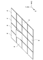
本実施の形態による光学デバイスでは、図6に示すように、前述した図1乃至図4に示す単位素子が基板1上に2次元状に配置されている。これにより、本実施の形態による光学デバイスは、空間光変調器を構成している。なお、図6では、簡単のため、4×4個の単位素子をアレイ化したものとしたが、その数は幾つでも構わない。図6において、1つのミラー4は、1つの単位素子に対応しているが、簡単のため、各単位素子のミラー4以外の構成要素の図示は省略している。なお、単位素子の並べ方は、図6に示す例に限定されるものではなく、例えば、列毎または行毎に半ピッチづつずらすなどの並べ方を採用してもよい。また、単位素子を1次元状に並べてもよい。なお、図6では、2行目2列目のミラー4が図5(c)に示す状態になっているとともに、他のミラー4は図5(a)に示す状態になっている。本実施の形態では、図5(b)に示す状態は用いずに図5(c)の状態を利用するようになっているが、逆に図5(b)に示す状態の方を用いるようにしてもよい。
In the optical device according to the present embodiment, as shown in FIG. 6, the above-described unit elements shown in FIGS. 1 to 4 are two-dimensionally arranged on the
本実施の形態による光学デバイスでは、図面には示していないが、各単位素子のミラー4の状態が制御信号に応じた状態となるように、各単位素子の電極間の電圧状態を決定する駆動回路が採用される。このような駆動回路としては、例えばDMD等と同様の駆動回路を採用することができるが、本実施の形態によるアレイ化した光学デバイス(この光学デバイスの各単位素子からミラー4を除いたものがマイクロアクチュエータアレーをなす。)は、チップ上において、図11に示す回路構成を有している。この回路構成については、後述する。
In the optical device according to the present embodiment, although not shown in the drawing, driving for determining the voltage state between the electrodes of each unit element so that the state of the
ここで、本実施の形態による光学デバイスの製造方法の一例について、特に前記単位素子に着目して、図7乃至図9を参照して説明する。図7乃至図9は、各製造工程を示す断面図であり、図4に対応している。 Here, an example of the manufacturing method of the optical device according to the present embodiment will be described with reference to FIGS. 7 to 9, particularly focusing on the unit element. 7 to 9 are cross-sectional views showing the respective manufacturing steps and correspond to FIG.
まず、シリコン基板上1に、酸化シリコン膜6を成膜する。次いで、アルミニウム膜を成膜し、フォトリソエッチング法により、そのアルミニウム膜を、固定電極5及び配線パターン7の形状にパターニングする(図7(a))。
First, a
次に、平坦化膜となるべき酸化シリコン膜20を成膜する(図7(b))。引き続いて、酸化シリコン膜20をCMPにより平坦化して平坦化膜とし、この平坦化膜20において、脚部3を形成すべき位置にコンタクトホール20aを、フォトリソグラフィにより形成する(図7(c))。なお、コンタクトホール20aは、後述の犠牲層21と窒化シリコン膜8を形成した後にも形成でき、この場合は犠牲層21をより平坦度良く形成できる。
Next, a
引き続いて、スピン塗布によりフォトレジスト等の犠牲層21を形成し、犠牲層21において脚部3を形成すべき位置に開口21aをフォトリソグラフィにより形成する(図8(a))。
Subsequently, a
その後、窒化シリコン膜8、アルミニウム膜9及び窒化シリコン膜10を順に成膜し、これらの膜8〜10を、フォトリソエッチング法により板状部材2の形状にパターニングする(図8(b))。このとき、エッチングを行なう工程は、成膜毎でもよいし、全ての膜を成膜し終わってから、その後上層膜から順にエッチングを加えても良いし、それらを組み合わせることもできる。なお、脚部3においてアルミニウム膜9が配線パターン7と電気的に接続されるように、窒化シリコン膜8には脚部3において開口を形成しておく。
Thereafter, a
次に、窒化シリコン膜10において接続部11を形成すべき位置に、開口10aをフォトリソグラフィにより形成する。また、フォトレジスト等の犠牲層22を形成し、犠牲層22において接続部11を形成すべき位置に開口22aをフォトリソグラフィにより形成する(図9(a))。なお、ミラー4は必ずしもアルミニウム膜9と電気的に接続する必要はないので、開口10aは必ずしも形成する必要はない。
Next, an opening 10 a is formed by photolithography at a position where the
次いで、アルミニウム膜を成膜し、フォトリソエッチング法により、このアルミニウム膜をミラー4の形状にパターニングする(図9(b))。最後に、プラズマアッシング等により、犠牲層21,22を除去する。これにより、本実施の形態による光学デバイスが完成する。
Next, an aluminum film is formed, and this aluminum film is patterned into the shape of the
本実施の形態では、前述したように、図4に示すように、平坦化膜20が形成されることで基体における板状部材2との対向領域が平坦化され、基体における板状部材2との対向領域と板状部材2との間には、空隙dが形成されている。この空隙dは、後述する静定時間を短縮するためには、0.3μm以下であることが好ましく、例えば、0.25μm程度とされる。
In the present embodiment, as described above, as shown in FIG. 4, by forming the
図4に示すように、板状部材2の下方の領域には、部分的に固定電極5及び配線パターン7が形成されているが、これによる凹凸形状が板状部材2に転写されてしまわないようにする必要がある。板状部材2にその凹凸形状が転写されてしまうと、前述した板状部材2の撓み動作に支障を来すためである。本実施の形態では、前記凹凸形状が板状部材2に転写されないようにするため、前述したようにCMPにより平坦化された平坦化膜20が形成され、基体における板状部材2との対向領域が平坦化されている。
As shown in FIG. 4, the fixed
これに対し、前記凹凸形状が板状部材2に転写されないようにするには、平坦化膜20を形成せずに、基体における板状部材2との対向領域を平坦化しないまま、図7(a)に示す状態の基板上に直接に、フォトレジストによる犠牲層21をスピン塗布することとし、犠牲層21を十分に厚くしてもよい。犠牲層21を十分に厚くすれば、犠牲層21の上面を平坦化することが可能であり、板状部材2への前記凹凸形状の転写を防ぐことができる。しかしながら、この場合、犠牲層21の上面を十分に平坦化するには、犠牲層21を十分に厚くする必要があるため、基体における板状部材2との対向領域と板状部材2との間の空隙が、かなり広くなってしまい、0.3μm以下にすることはできない。
On the other hand, in order to prevent the uneven shape from being transferred to the plate-
基体における板状部材2との対向領域と板状部材2との間の空隙が広いと、駆動の高速化に悪影響を及ぼす。その理由を以下に述べる。本実施の形態で用いられているようなマイクロアクチュエータでは、微細化すると、一般的に大きなQ値を有するため、一旦板状部材2等が振動すると、なかなか静定しない傾向がある。そして、基体における板状部材2との対向領域と板状部材2との間の空隙が十分に狭ければ、スクイーズドフィルムダンピング効果が顕著に現れ、駆動する際の振動が減衰して静定するまでの時間(静定時間)が短くなるが、前記空隙が広いと、スクイーズドフィルムダンピング効果が低下してしまい、静定時間が長くなり、駆動の高速化に悪影響を及ぼすのである。
If the gap between the region facing the plate-
したがって、前記凹凸形状が板状部材2に転写されないようにするために平坦化膜20を形成せずに犠牲層21を厚くすることは、駆動の高速化に悪影響を及ぼすのである。
Therefore, increasing the thickness of the
これに対し、本実施の形態では、平坦化膜20が形成されて基体における板状部材2との対向領域が平坦化されているので、犠牲層21を薄くしても、凹凸形状が板状部材2に転写されない。したがって、犠牲層21の厚さを0.3μm以下などのように薄くすることができ、これにより、スクイーズドフィルムダンピング効果が顕著に現れ、静定時間が短縮され、駆動の高速化を図ることができる。この場合のスクイーズドフィルムダンピング効果は、板状部材2が駆動の際にその周囲の空気(ガス)から空気抵抗を受けることで生じ、空隙dを狭くすることによって、この空気抵抗が効果的に大きくなる。
On the other hand, in the present embodiment, since the
本発明者は、空隙dを0.25μmとして、本実施の形態と同様の光学デバイスを作製した。その光学デバイスの駆動特性の実験結果を図10に示す。その実験では、図10に示すように固定電極5と可動電極との間に一周期毎に正負を反転させた方形波の駆動電圧を印加し、ミラー4にレーザー光を当て、その反射光の強度をフォトダイオードで計測した。反射光の強度の計測は、ミラー4の角度(基板1と平行である角度を基準とした角度)が0degと1.8degで出力が最大になる位置の2カ所で行った。図10から、この実験では、ミラー4の両角度間の切り換えを、静定時間を含めて3μsec以下と非常に短い時間で行うことができることがわかる。
The inventor manufactured an optical device similar to that of the present embodiment with the gap d being 0.25 μm. The experimental results of the drive characteristics of the optical device are shown in FIG. In the experiment, as shown in FIG. 10, a square-wave drive voltage in which positive and negative are reversed every cycle is applied between the fixed
図11は、本実施の形態による光学デバイスのチップ上の回路構成を示す電気回路図である。図1乃至図4に示す単一の単位素子(ひいては、単一のマイクロアクチュエータ)は、電気回路的には、1個のコンデンサ(固定電極5と前記可動電極(アルミニウム膜9の、固定電極5と対向する領域)とがなすコンデンサに相当)と見なせる。図11では、m行目n列目の単位素子のコンデンサをそれぞれCmnと表記している。例えば、図11中の左上の(1行目1列目の)単位素子のコンデンサをC11と表記している。本実施の形態では、各コンデンサの図11中の左側電極が固定電極5、図11中の右側電極が可動電極となっている。
FIG. 11 is an electric circuit diagram showing a circuit configuration on the chip of the optical device according to the present embodiment. A single unit element (and hence a single microactuator) shown in FIGS. 1 to 4 has one capacitor (a
図11では、説明を簡単にするため、9個の単位素子を3行3列に配置している。もっとも、単位素子の数は何ら限定されるものではなく、他の数の場合も原理は同一である。また、単位素子の数が同じであっても、行数と列数を同数にする必要はないし、マトリクス配置にする必要もない。 In FIG. 11, nine unit elements are arranged in 3 rows and 3 columns in order to simplify the description. However, the number of unit elements is not limited at all, and the principle is the same for other numbers. Further, even if the number of unit elements is the same, it is not necessary to make the number of rows and columns the same, and it is not necessary to make a matrix arrangement.
本実施の形態でによる光学デバイスには、図11に示すように、複数の端子CD1〜CD3からなる第1の複数の端子群、及び、複数の端子CU1〜CU3からなる第2の端子群が設けられている。これらの端子CD1〜CD3,CU1〜CU3は、外部接続用の端子である。本実施の形態では、前述した脚部3の下の配線パターン7及び固定電極5の配線パターンによって、図11に示す電気的な接続が実現されている。端子CD1〜CD3,CU1〜CU3は、例えば、これらの配線パターンの一部を電極パッドとすることにより構成することができる。
As shown in FIG. 11, the optical device according to the present embodiment includes a first plurality of terminal groups composed of a plurality of terminals CD1 to CD3 and a second terminal group composed of a plurality of terminals CU1 to CU3. Is provided. These terminals CD1 to CD3 and CU1 to CU3 are terminals for external connection. In the present embodiment, the electrical connection shown in FIG. 11 is realized by the
また、図11では、第1の端子群の端子CD1〜CD3の数が単位素子の行数と同じく3個とされ、第2の端子群の端子CU1〜CU3の数が単位素子の列数と同じく3個とされている。もっとも、第1及び第2の端子群の数は、単位素子の行数や列数と必ずしも同一にする必要はなく、例えば、下記の条件(a)〜(e)を満たせばよい。すなわち、(a)各マイクロアクチュエータに関して、当該マイクロアクチュエータの固定電極5が、前記第1及び第2の端子群のうちの一方の端子群のいずれか1つの端子に電気的に接続されるとともに前記第1及び第2の端子群の他の端子に電気的に接続されないこと、(b)各マイクロアクチュエータに関して、当該マイクロアクチュエータの可動電極が、前記第1及び第2の端子群のうちの他方の端子群のいずれか1つの端子に電気的に接続されるとともに前記第1及び第2の端子群の他の端子に電気的に接続されないこと、(c)各マイクロアクチュエータに関して、当該マイクロアクチュエータの前記固定電極5に電気的に接続された第1又は第2の端子群の1つの端子と当該マイクロアクチュエータの可動電極に電気的に接続された前記第1又は第2の端子群の1つの端子との組み合わせは、当該マイクロアクチュエータに固有のものとなること、(d)前記第1の端子群の少なくとも1つの端子が、当該光学デバイスに搭載されている複数のマイクロアクチュエータのうちの2つ以上のマイクロアクチュエータの固定電極5又は可動電極に、共通して電気的に接続されること、(e)前記第2の端子群の少なくとも1つの端子が、当該光学デバイスに搭載されている複数のマイクロアクチュエータのうちの2つ以上のマイクロアクチュエータの固定電極5又は可動電極に、共通して電気的に接続されること、の各条件を満たせばよい。
Further, in FIG. 11, the number of terminals CD1 to CD3 of the first terminal group is three as the number of rows of unit elements, and the number of terminals CU1 to CU3 of the second terminal group is the number of columns of unit elements. There are also three. However, the number of first and second terminal groups is not necessarily the same as the number of rows and columns of unit elements, and for example, the following conditions (a) to (e) may be satisfied. That is, (a) for each microactuator, the fixed
前記条件(a)〜(e)を満たす一例として、図11に示す例では、1行目のコンデンサC11,C12,C13の固定電極5は、第1の端子群の端子CD1に共通して電気的に接続され、その他の端子には電気的に接続されていない。2行目のコンデンサC21,C22,C23の固定電極5は、第1の端子群の端子CD2に共通して電気的に接続され、その他の端子には電気的に接続されていない。3行目のコンデンサC31,C32,C33の固定電極5は、第1の端子群の端子CD3に共通して電気的に接続され、その他の端子には電気的に接続されていない。また、1列目のコンデンサC11,C21,C31の可動電極は、第2の端子群の端子CU1に共通して電気的に接続され、その他の端子には電気的に接続されていない。2列目のコンデンサC12,C22,C32の可動電極は、第2の端子群の端子CU2に共通して電気的に接続され、その他の端子には電気的に接続されていない。3列目のコンデンサC13,C23,C33の可動電極は、第2の端子群の端子CU3に共通して電気的に接続され、その他の端子には電気的に接続されていない。
As an example satisfying the conditions (a) to (e), in the example shown in FIG. 11, the fixed
本実施の形態では、図示しない外部制御回路が、前記端子CD1〜CD3,CU1〜CU3に接続され、これらの端子の電位をそれぞれ独立して制御することで、各単位素子の状態の切り換え(例えば、図5(a)に示す状態と図5(c)に示す状態との間の切り換え)を制御する。前記外部制御回路は、指令信号に応答して当該指令信号が示す切換状態を実現するための制御信号を、各端子CD1〜CD3,CU1〜CU3に与える電位として供給する。 In the present embodiment, an external control circuit (not shown) is connected to the terminals CD1 to CD3 and CU1 to CU3, and the potentials of these terminals are controlled independently to switch the state of each unit element (for example, , Switching between the state shown in FIG. 5A and the state shown in FIG. The external control circuit supplies a control signal for realizing a switching state indicated by the command signal in response to the command signal as a potential to be applied to the terminals CD1 to CD3 and CU1 to CU3.
図12は、外部制御回路が各端子CD1〜CD3,CU1〜CU3に与える電位のタイミングチャートの一例を示すものである。図12に示す例では、外部制御回路は、各端子CD1〜CD3,CU1〜CU3には、電位±Vh,±Vm,0のいずれかの電位を与える。図12に示す例では、交流駆動が採用されている。ここで、Vh,Vmは0を基準とした正の値とし、Vh>Vmとする。もっとも、各電位の絶対値は、それらの相対的な関係を変えなければ、任意の電位レベルを基準として定めてもよいことは、言うまでもない。 FIG. 12 shows an example of a timing chart of potentials applied to the terminals CD1 to CD3 and CU1 to CU3 by the external control circuit. In the example shown in FIG. 12, the external control circuit applies any one of potentials ± Vh, ± Vm, 0 to the terminals CD1 to CD3 and CU1 to CU3. In the example shown in FIG. 12, AC driving is adopted. Here, Vh and Vm are positive values with reference to 0, and Vh> Vm. However, it goes without saying that the absolute value of each potential may be determined on the basis of any potential level as long as the relative relationship between them is not changed.
図12に示す例では、時刻t1以前は、全てのアクチュエータは解放状態(図5(a)に示す状態)となっている。時刻t1において、9個の全てのアクチュエータはクランプ状態(図5(c)に示す状態)となる。Vhは2×Vhがアクチュエータのクランプ電圧Vc(解放状態からクランプ状態になる最小の電圧)より高い電圧でより高くなるように設定しておく。Vmは、Vmが図11の解放電圧Vr(クランプ状態から解放状態になる最大の電圧。Vr<Vc)より高くなりかつ2×Vmがクランプ電圧Vcより低くなるように、設定しておく。その後、時刻t1から時刻t8までで、全アクチュエータを一旦クランプ状態にし、そこから任意のアクチュエータを解放状態にする方法が示されている。一部のアクチュエータが解放状態の時点から、特定の解放状態とされたアクチュエータをクランプ状態にし、別のアクチュエータを解放状態にする場合が、時刻t9以降に示されている。図12に示す動作例は、特開2004−184564号公報の図16(したがって、当該公報の図13)に開示されている動作例と同様である。 In the example shown in FIG. 12, all actuators are in the released state (the state shown in FIG. 5A) before time t1. At time t1, all nine actuators are in a clamped state (the state shown in FIG. 5C). Vh is set so that 2 × Vh becomes higher at a voltage higher than the clamp voltage Vc of the actuator (minimum voltage from the released state to the clamped state). Vm is set so that Vm is higher than the release voltage Vr (maximum voltage from the clamped state to the released state; Vr <Vc) in FIG. 11 and 2 × Vm is lower than the clamped voltage Vc. Thereafter, from time t1 to time t8, a method is shown in which all actuators are once clamped and any actuator is released therefrom. A case where an actuator that is in a specific released state is clamped and another actuator is released from the time when some of the actuators are in the released state is shown after time t9. The operation example shown in FIG. 12 is the same as the operation example disclosed in FIG. 16 of JP-A-2004-184564 (thus, FIG. 13 of the publication).
本実施の形態による光学デバイスでは、チップ上の回路構成として前述した図11に示す回路構成が採用されているので、特開2004−184564号公報に開示されている技術と同様に、チップ上にアドレス回路等を搭載することなく外部接続用の端子数(すなわち、外部に引き出す配線の本数)を減らすことができる。 In the optical device according to the present embodiment, the circuit configuration shown in FIG. 11 described above is adopted as the circuit configuration on the chip, and therefore, on the chip as in the technique disclosed in Japanese Patent Application Laid-Open No. 2004-184564. It is possible to reduce the number of terminals for external connection (that is, the number of wires drawn to the outside) without mounting an address circuit or the like.
本実施の形態によれば、板状部材2が両持ち梁となっているので、前述した特許文献2に開示されたデバイスと同様に、トーションヒンジを用いる場合に比べて破損が生じ難くなり長寿命化を図ることができるとともに、固有振動数を高くすることができ、応答速度を速くすることができる。
According to the present embodiment, since the plate-
そして、本実施の形態によれば、前述した特許文献2に開示されたデバイスと異なり、ミラー4は、板状部材2と全体的に一体化されるのではなく、接続部11を介して、板状部材2の撓み変形可能な領域のうちの一部の部位に、局所的に機械的に接続されている。したがって、前述した図5に示すように、ミラー4自体を変形させずに、ミラー4の向きのみを変更することができる。
And according to this Embodiment, unlike the device disclosed by
さらに、本実施の形態によれば、前述したように、平坦化膜20が形成されることで基体における板状部材2との対向領域が平坦化されているので、基体における板状部材2との対向領域と板状部材2との間の空隙dを狭めることができる。したがって、本実施の形態によれば、前述したスクイーズドフィルムダンピング効果を高めることができるので、静定時間を短縮して駆動をより高速化することができる
Furthermore, according to the present embodiment, as described above, since the flattening
なお、本発明では、必ずしも前述した単位素子を基板1上に複数配置する必要はなく、前述した単位素子を基板1上に1つだけ配置してもよい。
In the present invention, it is not always necessary to arrange a plurality of the above-described unit elements on the
[第2の実施の形態] [Second Embodiment]
図13は、本発明の第2の実施の形態による投影表示装置(投射型表示装置)を示す概略構成図である。 FIG. 13 is a schematic configuration diagram showing a projection display device (projection display device) according to the second embodiment of the present invention.
本発明による投影表示装置は、光源31と、照明光学系32と、空間光変調器33と、吸光板34と、投影光学系35と、スクリーン36と、制御部37とを備えている。本実施の形態では、空間光変調器33として、前述した第1の実施の形態による光学デバイスが用いられている。
The projection display device according to the present invention includes a
光源31から発せられた照明光は、照明光学系32を通過した後、空間光変調器33に照射される。空間光変調器33の各単位素子はそれぞれそのミラー4が第1の角度(図5(a)に示す状態)あるいは第2の角度(図5(b)又は図5(c)に示す状態)を有しているとする。第1の角度では、入射光は第1の方向へ反射され、吸光板34に到達し、その光は消滅する。第2の角度では、入射光は第2の方向へ反射され、投影光学系35を通過した後、スクリーン36上に投影される。制御部37は、画像信号に従って空間光変調器33に制御信号を送って空間光変調器33を制御し、各単位素子のミラー4の角度を画像信号に応じて変更させる。この制御により、入力された画像信号が示す静止画像や動画像がスクリーン36上に形成できる。
The illumination light emitted from the
本実施の形態は、いわゆる白黒の表示装置の例であったが、カラー化も従来技術を流用することにより達成可能である。図示していないが、例えば、照明光学系32の中に、あるいは照明光学系32と空間光変調器33との間に、カラーホイールを設置する、あるいは、光源31を赤・青・緑の三色が時間分割制御できるようなものであるとし、空間光変調器33と同期させることによりカラー化が達成可能である。
Although this embodiment is an example of a so-called black and white display device, colorization can also be achieved by diverting the prior art. Although not shown, for example, a color wheel is installed in the illumination
なお、本発明による光学デバイスを用いた投影表示装置は、本実施の形態のようなタイプの表示装置に限定されるものではなく、種々のタイプの投影表示装置に用いることができる。投影画像表示装置の構成例としては、空間光変調器として、液晶パネルやDMDなどを用いたものが種々提案されている。DMDを用いた投影画像表示装置で使われる光学系については、本発明の光学デバイスによる空間光変調器がDMDと同様のミラー角度を変更するミラーデバイスであるため、基本的に全く同等のものが使用できる。液晶パネルを用いた投影画像表示装置は、原理的に偏光した光線を用い、また、反射型だけでなく、透過型のものもある。このため、本発明による光学デバイスによる空間光変調器にこれらの光学系を適応させる場合は、それらの点に関して変更を伴えばよい。 The projection display device using the optical device according to the present invention is not limited to the type of display device as in the present embodiment, and can be used for various types of projection display devices. As a configuration example of the projection image display device, various types using a liquid crystal panel, DMD, or the like as a spatial light modulator have been proposed. Regarding the optical system used in the projection image display apparatus using DMD, the spatial light modulator by the optical device of the present invention is a mirror device that changes the mirror angle similar to that of DMD, and therefore basically the same one is used. Can be used. Projection image display devices using a liquid crystal panel use polarized light in principle, and there are transmission types as well as reflection types. For this reason, when these optical systems are adapted to the spatial light modulator by the optical device according to the present invention, it is sufficient to change those points.
なお、空間光変調器を用いた応用用途としては、投影画像表示装置などの映像用途や、後述する露光装置のみならず、前述した光学的情報処理装置や静電写真印刷装置、さらに、光通信に使われる光スイッチやSwitched Blazed Grating Device、印刷分野で使われるプレートセッターなど様々な用途があるが、本発明もこれらに適応できる。 Note that the application using the spatial light modulator includes not only a video application such as a projection image display device and an exposure device described later, but also the optical information processing device and the electrophotographic printing device described above, and optical communication. There are various uses such as an optical switch used in the field, a Switched Blazed Grating Device, and a plate setter used in the printing field. The present invention is also applicable to these.
[第3の実施の形態] [Third Embodiment]
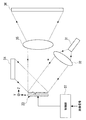
図14は、本発明の第3の実施の形態による露光装置100を示す概略構成図である。
FIG. 14 is a schematic block diagram showing an
本実施の形態による露光装置100は、照明系41、パターン生成装置42、投影光学系PL、ステージ装置43、反射ミラー44及び制御系等を含んでいる。この露光装置100は、パターン生成装置42で生成されたパターンの像(パターン像)をステージ装置43の一部を構成するステージSTに載置されたウエハW上に投影光学系PLを用いて形成するものである。前記制御系は、マイクロコンピュータを含み、装置全体を統括的に制御する主制御装置45を中心として構成されている。
The
照明系41は、光源ユニット及び光源制御系を含む光源系、並びにコリメートレンズ、オプティカルインテグレータ(フライアイレンズ、ロッド型インテグレータあるいは回折素子など)、集光レンズ、視野絞り、リレーレンズ等を含む照明光学系等(いずれも不図示)を含んでいる。この照明系41からは、照明光ILが射出される。
The
光源ユニットとしては、例えば国際公開第1999/46835号パンフレット(対応米国特許第7,023,610号明細書)に開示されているように、DFB半導体レーザ又はファイバレーザなどの固体レーザ光源、ファイバーアンプなどを有する光増幅部、及び波長変換部などを含み、波長193nmのパルス光を出力する高調波発生装置が用いられている。なお、光源ユニットは、例えば波長440nmの連続光又はパルス光を発生するレーザダイオードなどでも良い。 As the light source unit, for example, as disclosed in International Publication No. 1999/46835 pamphlet (corresponding US Pat. No. 7,023,610), solid laser light source such as DFB semiconductor laser or fiber laser, fiber amplifier, etc. A harmonic generator that outputs pulsed light having a wavelength of 193 nm is used. Note that the light source unit may be, for example, a laser diode that generates continuous light or pulsed light having a wavelength of 440 nm.
反射ミラー44は、照明系41から射出される照明光ILをパターン生成装置42の後述する可変成形マスクVMに向けて反射する。なお、この反射ミラー44は、実際には、照明系41内部の照明光学系の一部を構成するものであるが、ここでは、説明の便宜上から照明系41の外部に取り出して示されている。
The
パターン生成装置42は、可変成形マスクVM及びミラー駆動系51等を含んでいる。可変成形マスクVMは、前記投影光学系PLの−Z側で、かつ反射ミラー44で反射された照明光ILの光路上に配置されている。本実施の形態では、可変成形マスクVMとして、前述した第1の実施の形態による光学デバイスが用いられている。本実施の形態では、図5(a)に示す状態の場合に、当該単位素子のミラー4に照明光ILが照射されると、照明光ILはミラー4で反射して、投影光学系PLに入射するとともに、図5(c)に示す状態(あるいは図5(b)に示す状態)の場合に、当該単位素子のミラー4に照明光ILが照射されると、当該単位素子のミラー4で反射された照明光は、投影光学系PLには入射しないようになっている。ミラー駆動系51は、主制御装置45の指示の下で可変成形マスクVMを駆動するものであり、前述した第1の実施の形態で説明した外部制御回路に相当する回路を含んでいる。
The
ミラー駆動系51は、不図示のインターフェースを介して不図示の上位装置からパターン像の形成に必要なデータのうちパターンの設計データ(例えば、CADデータ)を取得する。そして、ミラー駆動系51は、取得した設計データに基づいて、ウエハW上における露光対象の区画領域部分に可変成形マスクVMからの光が投影光学系PLを介して照射され、ウエハW上における露光対象の区画領域部分以外の部分に可変成形マスクVMからの光が照射されないように、各単位素子を駆動する信号を生成し、可変成形マスクVMに供給する。これにより、パターン生成装置42で、設計データに応じたパターンが生成される。なお、パターン生成装置42で生成されるパターンは、ウエハWの走査方向(ここでは、X軸方向)への移動に伴って変化する。
The
投影光学系PLは、鏡筒の内部に所定の位置関係で配置された複数の光学素子を有する。投影光学系PLは、パターン生成装置42で生成されたパターンを、被露光面上に配置されたウエハW上に投影倍率βで縮小投影する。
Projection optical system PL has a plurality of optical elements arranged in a predetermined positional relationship inside the lens barrel. The projection optical system PL projects the pattern generated by the
ステージ装置43は、露光対象のウエハWを投影光学系PLに対してアライメントした状態でXY面内で移動させるためのものであり、ステージSTと、該ステージSTの駆動を制御するステージ駆動系52とを備えている。
The
ステージSTは、ステージ駆動系52により駆動されてXY面内及びZ軸方向に3次元的に移動し、あるいは投影光学系PLの像面に対して適宜傾斜することによって投影光学系PLを介したパターン像に対してウエハWをアライメント可能である。さらに、ステージSTは、ステージ駆動系52により駆動されて走査方向に所望の速度で移動させることができる。
The stage ST is driven by the
主制御装置45は、照明系41、パターン生成装置42、ステージ装置43等を適当なタイミングで動作させて、ウエハW上の適所にパターン生成装置42で生成されたパターンの像を投影光学系PLを介して投影する。このとき、主制御装置45は、ステージ装置43によるウエハWの移動に同期して、ミラー駆動系51に可変成形マスクVMを制御させる。
The
本発明の一実施の形態によるデバイス製造方法では、半導体デバイスは、デバイスの機能・性能設計を行う工程、シリコン材料からウエハを形成する工程、上記の実施の形態の露光装置100により可変成形マスクVMを介してウエハWを露光する工程を含むリソグラフィ工程、エッチング等の回路パターンを形成する工程、デバイス組み立て工程(ダイシング工程、ボンディング工程、パッケージ工程を含む)、及び検査工程等を経て製造される。なお、本発明は、半導体デバイス製造用の露光装置のみならず、他の種々のデバイスを製造するための露光装置にも適用することができる。
In the device manufacturing method according to the embodiment of the present invention, the semiconductor device includes a step of performing function / performance design of the device, a step of forming a wafer from a silicon material, and the variable forming mask VM by the
[第4の実施の形態] [Fourth Embodiment]
図15は、本発明の第4の実施の形態による光学デバイスの単位素子の板状部材2を模式的に示す概略平面図であり、図3に対応している。図15において、図3中の要素と同一又は対応する要素には同一符号を付し、その重複する説明は省略する。
FIG. 15 is a schematic plan view schematically showing the plate-
本実施の形態による光学デバイスが前記第1の実施の形態による光学デバイスと異なる所は、前記第1の実施の形態では、板状部材2がその2辺付近のみで脚部3を介して基板1に対して固定されていたのに対し、本実施の形態では、板状部材2がその4辺付近で脚部3を介して基板1に対して固定されている点のみである。本実施の形態によっても、前記第1の実施の形態と同様の利点が得られる。
The optical device according to the present embodiment is different from the optical device according to the first embodiment in that, in the first embodiment, the plate-
[第5の実施の形態] [Fifth Embodiment]
図16は、本発明の第5の実施の形態による光学デバイスの単位素子を模式的に示す概略断面図であり、図4に対応している。図16において、図4中の要素と同一又は対応する要素には同一符号を付し、その重複する説明は省略する。 FIG. 16 is a schematic cross-sectional view schematically showing a unit element of an optical device according to the fifth embodiment of the present invention, and corresponds to FIG. 16, elements that are the same as or correspond to the elements in FIG. 4 are given the same reference numerals, and redundant descriptions thereof are omitted.
本実施の形態による光学デバイスが前記第1の実施の形態による光学デバイスと異なる所は、接続部11がミラー4の中心に配置されている点と、接続部11が板状部材2の中心に固定されている点と、板状部材2のX軸方向の中央付近において基板1上に形成されていた1つの固定電極5に代えて、板状部材2の−X側と+X側にX軸方向に関して対称的な位置に2つの固定電極5a,5bが基板1上に形成されている点と、全体として連続した1つのアルミニウム膜9が、−X側と+X側の2つのアルミニウム膜9a,9bに分離されている点のみである。
The optical device according to the present embodiment is different from the optical device according to the first embodiment in that the
なお、本実施の形態においても、前記第1の実施の形態と同様に、板状部材2との対向領域を含む基板1上の領域において、配線パターン7、固定電極5a,5b及び絶縁膜6を覆うように、酸化シリコン膜等からなる平坦化膜20が形成されることで、基体における板状部材2との対向領域が平坦化されている。
In the present embodiment, similarly to the first embodiment, in the region on the
本実施の形態では、アルミニウム膜9aの、固定電極5aと対向する領域9a’が、固定電極5aとの間の電圧により固定電極5aとの間に静電力を生じ得る可動電極となっている。また、アルミニウム膜9bの、固定電極5bと対向する領域9b’が、固定電極5bとの間の電圧により固定電極5bとの間に静電力を生じ得る可動電極となっている。
In the present embodiment, the
図17及び図18は、本実施の形態による光学デバイスの各動作状態を模式的に示す図であり、図16を大幅に簡略化した断面図に相当している。 FIGS. 17 and 18 are diagrams schematically showing each operation state of the optical device according to the present embodiment, and correspond to a cross-sectional view that greatly simplifies FIG.
図17(a)は、図16と同じく、電極5a,電極9a’間及び電極5b,電極9b’間にそれぞれ電圧を印加せず、それらの間に静電力を発生させない状態を示している。この状態では、板状部材2は変形しておらず、平坦形状になっている。このため、ミラー4は、基板1に対して平行を維持している。
FIG. 17A shows a state where no voltage is applied between the
図17(b)は、電極5a,9a’間に比較的高い電圧を印加して両者の間に比較的大きい静電力を発生させる一方、電極5b,電極9b’間に電圧を印加せずそれらの間に静電力を発生させない状態を示している。この状態では、板状部材2は、電極9a’付近で電極5a付近に当接するが、電極5b,9b’の間隔は比較的大きくなっている。この状態では、ミラー4が比較的大きく図中の左側へ傾いている。
FIG. 17B shows that a relatively high voltage is applied between the
図17(c)は、電極5b,9b’間に比較的高い電圧を印加して両者の間に比較的大きい静電力を発生させる一方、電極5a,電極9a’間に電圧を印加せずそれらの間に静電力を発生させない状態を示している。この状態では、板状部材2は、電極9b’付近で電極5b付近に当接するが、電極5a,9a’の間隔は比較的大きくなっている。この状態では、ミラー4が比較的大きく図中の右側へ傾いている。
In FIG. 17C, a relatively high voltage is applied between the
図18(a)は、電極5b,9b’間にさほど高くない電圧を印加して両者の間に静電力を発生させる一方、電極5a,電極9a’間に電圧を印加せずそれらの間に静電力を発生させない状態を示している。この状態では、板状部材2は、電極9b’付近で電極5b付近に近づくが、電極5a,9a’の間隔は比較的大きくなっている。この状態では、ミラー4がさほど大きくなく図中の右側へ傾いている。その傾き角度は、電極5b,9b’間に印加する電圧を調整することで、調整可能である。
In FIG. 18A, a not so high voltage is applied between the
図面には示していないが、図18(a)の場合と逆に、電極5a,9a’間にさほど高くない電圧を印加して両者の間に静電力を発生させる一方、電極5b,電極9b’間に電圧を印加せずそれらの間に静電力を発生させない状態にすると、板状部材2は、電極9a’付近で電極5a付近に近づくが、電極5b,9b’の間隔は比較的大きくなる。この状態では、ミラー4がさほど大きくなく図中の左側へ傾く。その傾き角度は、電極5a,9a’間に印加する電圧を調整することで、調整可能である。
Although not shown in the drawing, contrary to the case of FIG. 18 (a), a not so high voltage is applied between the
図18(b)は、電極5a,9a’間及び電極5b,電極9b’間にそれぞれ比較的高い電圧を印加してそれら間に比較的大きい静電力を発生させた状態を示している。この状態では、板状部材2は、電極9a’付近で電極5a付近に当接するとともに、電極9b’付近で電極5b付近に当接している。この状態では、ミラー4は、基板1に対して平行を維持したまま、最も低い位置に位置している。
FIG. 18B shows a state in which a relatively high voltage is applied between the
図18(c)は、電極5a,9a’間及び電極5b,電極9b’間にそれぞれさほど高くない電圧を印加してそれら間にさほど大きくない静電力を発生させた状態を示している。この状態では、板状部材2は、電極9a’付近で電極5a付近に近づくとともに、電極9b’付近で電極5b付近に同程度近づいている。この状態では、ミラー4は、基板1に対して平行を維持したまま、中間の高さ位置に位置している。その高さは、電極5a,9a’間及び電極5b,9b’間に印加する電圧を調整することで、調整可能である。
FIG. 18C shows a state in which a not so high voltage is applied between the
このように、本実施の形態によれば、図17(a)〜(c)及び図18(a)に示すように、ミラー4の傾きを変化させることができるだけではなく、図17(a)、図18(b)(c)に示すように、ミラー4を基板1に対して平行に維持したまま、高さを変えることができる。
Thus, according to the present embodiment, as shown in FIGS. 17A to 17C and FIG. 18A, not only can the inclination of the
よって、本実施の形態によれば、反射光の方向を変えることができるのみならず、ミラー4を傾けることなく高さ位置を変えることで反射光の光学距離を変えて反射光の位相をシフトさせることが可能となり、位相変調器としても用いることができる。したがって、本実施の形態による光学デバイスを、前記第3の実施の形態のような露光装置において可変成形マスクVMとして用いれば、位相シフトマスクとして機能させることもできる。
Therefore, according to the present embodiment, not only the direction of the reflected light can be changed, but also the optical distance of the reflected light is changed by changing the height position without tilting the
これ以外については、本実施の形態によっても前記第1の実施の形態と同様の利点が得られる。 Except for this, the present embodiment can provide the same advantages as those of the first embodiment.
以上、本発明の各実施の形態について説明したが、本発明はこれらの実施の形態に限定されるものではない。 Although the embodiments of the present invention have been described above, the present invention is not limited to these embodiments.
1 基板
2 板状部材
4 ミラー
5 固定電極
20 平坦化膜
1
Claims (17)
前記板状部材は、前記板状部材の周辺部における全周又はその一部に渡る所定箇所で前記基体に対して固定されて、前記板状部材における前記所定箇所以外の領域で撓み変形可能であり、
前記所定箇所は、前記板状部材の前記周辺部において互いに対向する2箇所を含み、
被駆動体が、前記板状部材の撓み変形可能な領域のうちの所定部位に局所的に機械的に接続され、
前記駆動力付与手段は、信号に応じて、前記板状部材の前記撓み変形可能な領域が撓み変形をして前記板状部材の前記所定部位の傾きが変化するように、前記板状部材の少なくとも一部に駆動力を付与し得るものであり、
前記基体における前記板状部材との対向領域が平坦化され、
前記駆動力付与手段は、前記基体に設けられた1つ以上の第1の電極部と、前記板状部材に設けられ前記1つ以上の第1の電極部との間の電圧により前記1つ以上の第1の電極部との間に静電力を生じ得る1つ以上の第2の電極部とを、含む、
ことを特徴とするマイクロアクチュエータ。 A base, a plate-like member supported by the base, and a driving force applying means;
The plate-like member is fixed to the base at a predetermined location over the entire circumference or a part of the periphery of the plate-like member, and can be bent and deformed in a region other than the predetermined location in the plate-like member. Yes,
The predetermined location includes two locations facing each other in the peripheral portion of the plate-shaped member,
A driven body is locally mechanically connected to a predetermined portion of the plate-shaped member in a deformable region;
In response to the signal, the driving force applying means is configured so that the region of the plate-like member that can be bent and deformed is bent and the inclination of the predetermined portion of the plate-like member is changed. A driving force can be imparted to at least a part thereof,
The opposing area | region with the said plate-shaped member in the said base | substrate is planarized,
The driving force applying means may be configured such that the one or more first electrode portions provided on the base and the one or more first electrode portions provided on the plate-like member by a voltage between them. Including one or more second electrode parts capable of generating an electrostatic force between the first electrode part and the first electrode part,
A microactuator characterized by that.
前記板状部材は、前記板状部材の周辺部における全周又はその一部に渡る所定箇所で前記基体に対して固定されて、前記板状部材における前記所定箇所以外の領域で撓み変形可能であり、
前記所定箇所は、前記板状部材の前記周辺部において互いに対向する2箇所を含み、
被駆動体が、前記板状部材の撓み変形可能な領域のうちの所定部位に局所的に機械的に接続され、
前記駆動力付与手段は、信号に応じて、前記板状部材の前記撓み変形可能な領域が撓み変形をして前記板状部材の前記所定部位の傾きが変化するように、前記板状部材の少なくとも一部に駆動力を付与し得るものであり、
前記基体における前記板状部材との対向領域が平坦化され、
前記板状部材の前記所定部位は、前記板状部材の重心から偏心した部位である、
ことを特徴とするマイクロアクチュエータ。 A base, a plate-like member supported by the base, and a driving force applying means;
The plate-like member is fixed to the base at a predetermined location over the entire circumference or a part of the periphery of the plate-like member, and can be bent and deformed in a region other than the predetermined location in the plate-like member. Yes,
The predetermined location includes two locations facing each other in the peripheral portion of the plate-shaped member,
A driven body is locally mechanically connected to a predetermined portion of the plate-shaped member in a deformable region;
In response to the signal, the driving force applying means is configured so that the region of the plate-like member that can be bent and deformed is bent and the inclination of the predetermined portion of the plate-like member is changed. A driving force can be imparted to at least a part thereof,
The opposing area | region with the said plate-shaped member in the said base | substrate is planarized,
The predetermined part of the plate-like member is a part eccentric from the center of gravity of the plate-like member.
A microactuator characterized by that.
前記各マイクロアクチュエータは、請求項1乃至6のいずれかに記載のマイクロアクチュエータであり、
前記各マイクロアクチュエータに関して、当該マイクロアクチュエータの前記第1の電極部が、前記第1及び第2の端子群のうちの一方の端子群のいずれか1つの端子に電気的に接続されるとともに前記第1及び第2の端子群の他の端子に電気的に接続されず、
前記各マイクロアクチュエータに関して、当該マイクロアクチュエータの前記第2の電極部が、前記第1及び第2の端子群のうちの他方の端子群のいずれか1つの端子に電気的に接続されるとともに前記第1及び第2の端子群の他の端子に電気的に接続されず、
前記各マイクロアクチュエータに関して、当該マイクロアクチュエータの前記第1の電極部に電気的に接続された第1又は第2の端子群の1つの端子と当該マイクロアクチュエータの前記第2の電極部に電気的に接続された前記第1又は第2の端子群の1つの端子との組み合わせは、当該マイクロアクチュエータに固有のものとなり、
前記第1の端子群の少なくとも1つの端子が、前記複数のマイクロアクチュエータのうちの2つ以上のマイクロアクチュエータの前記第1又は第2の電極部に、共通して電気的に接続され、
前記第2の端子群の少なくとも1つの端子が、前記複数のマイクロアクチュエータのうちの2つ以上のマイクロアクチュエータの前記第1又は第2の電極部に、共通して電気的に接続された、
ことを特徴とするマイクロアクチュエータアレー。 A microactuator array comprising a plurality of microactuators, a first terminal group consisting of a plurality of terminals, and a second terminal group consisting of a plurality of terminals,
Each of the microactuators is a microactuator according to any one of claims 1 to 6,
For each of the microactuators, the first electrode portion of the microactuator is electrically connected to one terminal of one of the first and second terminal groups and the first Not electrically connected to the other terminals of the first and second terminal groups,
For each of the microactuators, the second electrode portion of the microactuator is electrically connected to one terminal of the other terminal group of the first and second terminal groups and the first Not electrically connected to the other terminals of the first and second terminal groups,
Regarding each microactuator, one terminal of the first or second terminal group electrically connected to the first electrode portion of the microactuator and the second electrode portion of the microactuator are electrically connected. The combination with one terminal of the connected first or second terminal group is specific to the microactuator,
At least one terminal of the first terminal group is electrically connected in common to the first or second electrode portion of two or more microactuators of the plurality of microactuators;
At least one terminal of the second terminal group is electrically connected in common to the first or second electrode portion of two or more microactuators of the plurality of microactuators;
A microactuator array characterized by that.
前記照明光の光路上に配置される請求項11記載の光学デバイスを備え、
該光学デバイスを介した前記照明光を用いて前記物体を露光することを特徴とする露光装置。 An exposure apparatus that exposes an object using illumination light,
The optical device according to claim 11 disposed on an optical path of the illumination light,
An exposure apparatus that exposes the object using the illumination light that passes through the optical device.
前記光学デバイスの前記各マイクロアクチュエータの前記駆動力付与手段は、前記移動体の所定方向への移動に同期して制御されることを特徴とする請求項13又は14記載の露光装置。 A moving body that holds and moves the object;
The exposure apparatus according to claim 13 or 14, wherein the driving force applying means of each microactuator of the optical device is controlled in synchronization with the movement of the movable body in a predetermined direction.
前記リソグラフィ工程では、請求項13乃至15のいずれかに記載の露光装置を用いて露光を行うことを特徴とするデバイス製造方法。 A device manufacturing method including a lithography process,
16. A device manufacturing method comprising performing exposure using the exposure apparatus according to claim 13 in the lithography process.
前記基体に支持され、前記固定電極により撓み変形が可能な板状部材とを有するマイクロアクチュエータの製造方法であって、
前記基板上に前記絶縁膜を成膜することと、
前記固定電極が前記板状部材の一部と対向するとともに前記板状部材の残りの部分とは対向しないように、前記絶縁膜上に前記固定電極及び配線パターンを形成することと、
前記絶縁膜上と、前記固定電極及び配線パターン上における、前記板状部材との対向領域に平坦化膜となるべき膜を成膜することと、
前記平坦化膜となるべき膜を平坦化して平坦化膜とすることと、
前記平坦化膜上に犠牲層を形成することと、
前記犠牲層上に前記板状部材を形成することと、
を含み、
前記マイクロアクチュエータは請求項1乃至7のいずれかに記載のマイクロアクチュエータである、
ことを特徴とするマイクロアクチュエータの製造方法。 A substrate configured to include a substrate, an insulating film, a fixed electrode, and a wiring pattern;
A microactuator manufacturing method comprising a plate-like member supported by the base body and capable of being bent and deformed by the fixed electrode,
Depositing the insulating film on the substrate;
Forming the fixed electrode and the wiring pattern on the insulating film so that the fixed electrode faces a part of the plate-shaped member and does not face the remaining portion of the plate-shaped member;
Forming a film to be a planarizing film on the insulating film and on the fixed electrode and the wiring pattern in a region facing the plate-like member;
Flattening the film to be the flattened film into a flattened film;
Forming a sacrificial layer on the planarizing film;
Forming the plate-like member on the sacrificial layer;
Only including,
The microactuator is the microactuator according to any one of claims 1 to 7.
A manufacturing method of a microactuator characterized by the above.
Priority Applications (1)
| Application Number | Priority Date | Filing Date | Title |
|---|---|---|---|
| JP2007290577A JP5374860B2 (en) | 2007-11-08 | 2007-11-08 | Microactuator and manufacturing method thereof, microactuator array, microactuator device, optical device, display device, exposure apparatus, and device manufacturing method |
Applications Claiming Priority (1)
| Application Number | Priority Date | Filing Date | Title |
|---|---|---|---|
| JP2007290577A JP5374860B2 (en) | 2007-11-08 | 2007-11-08 | Microactuator and manufacturing method thereof, microactuator array, microactuator device, optical device, display device, exposure apparatus, and device manufacturing method |
Publications (3)
| Publication Number | Publication Date |
|---|---|
| JP2009118682A JP2009118682A (en) | 2009-05-28 |
| JP2009118682A5 JP2009118682A5 (en) | 2011-04-07 |
| JP5374860B2 true JP5374860B2 (en) | 2013-12-25 |
Family
ID=40785165
Family Applications (1)
| Application Number | Title | Priority Date | Filing Date |
|---|---|---|---|
| JP2007290577A Active JP5374860B2 (en) | 2007-11-08 | 2007-11-08 | Microactuator and manufacturing method thereof, microactuator array, microactuator device, optical device, display device, exposure apparatus, and device manufacturing method |
Country Status (1)
| Country | Link |
|---|---|
| JP (1) | JP5374860B2 (en) |
Families Citing this family (6)
| Publication number | Priority date | Publication date | Assignee | Title |
|---|---|---|---|---|
| NL1036321A1 (en) * | 2007-12-20 | 2009-06-29 | Asml Netherlands Bv | Device control method and apparatus. |
| JP5573212B2 (en) * | 2010-02-08 | 2014-08-20 | 株式会社ニコン | Spatial light modulation element, manufacturing method of spatial light modulation element, illumination light generator and exposure apparatus |
| JP5727005B2 (en) | 2010-07-01 | 2015-06-03 | カール・ツァイス・エスエムティー・ゲーエムベーハー | Optical system and multifaceted mirror |
| CA2880038C (en) * | 2012-07-27 | 2021-06-01 | Thorlabs, Inc. | Agile imaging system |
| JP5908422B2 (en) * | 2013-03-19 | 2016-04-26 | 株式会社東芝 | MEMS device and manufacturing method thereof |
| JP7260959B2 (en) * | 2018-03-16 | 2023-04-19 | キヤノン株式会社 | Lithographic apparatus, illumination apparatus and method of manufacturing an article |
Family Cites Families (11)
| Publication number | Priority date | Publication date | Assignee | Title |
|---|---|---|---|---|
| JPH03273869A (en) * | 1990-03-23 | 1991-12-05 | Murata Mfg Co Ltd | Piezoelectric actuator |
| JPH08293590A (en) * | 1995-04-21 | 1996-11-05 | Sony Corp | Manufacture of laminated substrate and transistor |
| JP2001350196A (en) * | 2000-06-06 | 2001-12-21 | Ricoh Co Ltd | Image display device |
| JP4766758B2 (en) * | 2001-02-28 | 2011-09-07 | 株式会社半導体エネルギー研究所 | Method for manufacturing semiconductor device |
| JP4146127B2 (en) * | 2002-01-16 | 2008-09-03 | セイコーインスツル株式会社 | Piezoelectric actuator and electronic device including the same |
| JP2003340795A (en) * | 2002-05-20 | 2003-12-02 | Sony Corp | Electrostatic drive type mems element and manufacturing method therefor, optical mems element, optical modulator, glv device and laser display |
| JP2004001110A (en) * | 2002-05-31 | 2004-01-08 | Ricoh Co Ltd | Electrostatic actuator, liquid droplet discharge head, ink jet recording device, and micro device |
| JP4042551B2 (en) * | 2002-12-02 | 2008-02-06 | 株式会社ニコン | Microactuator device and optical switch system |
| JP2006187060A (en) * | 2004-12-27 | 2006-07-13 | Nikon Corp | Micro actuator, manufacturing method thereof, optical device, and optical switch |
| JP2006256222A (en) * | 2005-03-18 | 2006-09-28 | Seiko Epson Corp | Electrostatic actuator, manufacturing method for electrostatic actuator, liquid droplet ejecting head, manufacturing method for liquid droplet ejecting head, liquid droplet ejector, manufacturing method for liquid droplet ejector, device and manufacturing method for device |
| JP2007214374A (en) * | 2006-02-09 | 2007-08-23 | Fujifilm Corp | Solid state image sensor and method of manufacturing same |
-
2007
- 2007-11-08 JP JP2007290577A patent/JP5374860B2/en active Active
Also Published As
| Publication number | Publication date |
|---|---|
| JP2009118682A (en) | 2009-05-28 |
Similar Documents
| Publication | Publication Date | Title |
|---|---|---|
| JP5609114B2 (en) | Microactuator, optical device, display device, exposure apparatus, and device manufacturing method | |
| JP5754656B2 (en) | Optical device, exposure apparatus, and device manufacturing method | |
| JP4694548B2 (en) | Spatial light modulator and method of manufacturing spatial light modulator | |
| US6914711B2 (en) | Spatial light modulator with hidden comb actuator | |
| US7400437B2 (en) | Discretely controlled micromirror with multi-level positions | |
| JP5374860B2 (en) | Microactuator and manufacturing method thereof, microactuator array, microactuator device, optical device, display device, exposure apparatus, and device manufacturing method | |
| US20040017599A1 (en) | Micro-mirror with rotor structure | |
| US20050275926A1 (en) | Variable focusing lens comprising micromirrors with one degree of freedom rotation | |
| JP4872453B2 (en) | Microactuator, optical device and display device | |
| WO2005085125A1 (en) | Micro actuator and device having micro actuator | |
| WO2006109687A1 (en) | Micromachine structure | |
| JP6809018B2 (en) | Light deflector, light scanning device, image forming device and image projection device | |
| JP2007192902A (en) | Method for driving micro-electro mechanical element, method for driving micro-electro mechanical element array, micro-electro mechanical element, micro-electro mechanical element array, and image forming apparatus | |
| WO2015145943A1 (en) | Optical scanning device | |
| JP2008046591A (en) | Method of producing contact part of actuator, actuator, optical system and image forming apparatus | |
| Cho et al. | Electrostatic 1D microscanner with vertical combs for HD resolution display | |
| Wang et al. | Highly space-efficient electrostatic zigzag transmissive micro-optic switches for an integrated MEMS optical display system | |
| JP5740819B2 (en) | Spatial light modulator manufacturing method, spatial light modulator, illumination light generator, and exposure apparatus | |
| JP2007188005A (en) | Optical modulation element, actuator and driving method of actuator | |
| WO2004074903A1 (en) | Scanning mirror with 2 degrees of freedom and manufacturing method thereof | |
| JP2006030585A (en) | Thin film member, micro-actuator, optical device, and optical switch | |
| JP2013171213A (en) | Spatial optical modulator and control method of the same, and exposure device | |
| KR20100045136A (en) | Optical modulator package and method thereof | |
| JP2006106215A (en) | Thin film structure body, optical apparatus, optical switch and variable optical attenuator |
Legal Events
| Date | Code | Title | Description |
|---|---|---|---|
| A621 | Written request for application examination |
Free format text: JAPANESE INTERMEDIATE CODE: A621 Effective date: 20101027 |
|
| A521 | Request for written amendment filed |
Free format text: JAPANESE INTERMEDIATE CODE: A523 Effective date: 20110217 |
|
| A977 | Report on retrieval |
Free format text: JAPANESE INTERMEDIATE CODE: A971007 Effective date: 20120629 |
|
| A131 | Notification of reasons for refusal |
Free format text: JAPANESE INTERMEDIATE CODE: A131 Effective date: 20120710 |
|
| A521 | Request for written amendment filed |
Free format text: JAPANESE INTERMEDIATE CODE: A523 Effective date: 20120819 |
|
| A131 | Notification of reasons for refusal |
Free format text: JAPANESE INTERMEDIATE CODE: A131 Effective date: 20130305 |
|
| A521 | Request for written amendment filed |
Free format text: JAPANESE INTERMEDIATE CODE: A523 Effective date: 20130402 |
|
| TRDD | Decision of grant or rejection written | ||
| A01 | Written decision to grant a patent or to grant a registration (utility model) |
Free format text: JAPANESE INTERMEDIATE CODE: A01 Effective date: 20130827 |
|
| A61 | First payment of annual fees (during grant procedure) |
Free format text: JAPANESE INTERMEDIATE CODE: A61 Effective date: 20130909 |
|
| R150 | Certificate of patent or registration of utility model |
Ref document number: 5374860 Country of ref document: JP Free format text: JAPANESE INTERMEDIATE CODE: R150 Free format text: JAPANESE INTERMEDIATE CODE: R150 |
|
| R250 | Receipt of annual fees |
Free format text: JAPANESE INTERMEDIATE CODE: R250 |
|
| R250 | Receipt of annual fees |
Free format text: JAPANESE INTERMEDIATE CODE: R250 |
|
| R250 | Receipt of annual fees |
Free format text: JAPANESE INTERMEDIATE CODE: R250 |
|
| R250 | Receipt of annual fees |
Free format text: JAPANESE INTERMEDIATE CODE: R250 |
|
| R250 | Receipt of annual fees |
Free format text: JAPANESE INTERMEDIATE CODE: R250 |
|
| R250 | Receipt of annual fees |
Free format text: JAPANESE INTERMEDIATE CODE: R250 |
|
| R250 | Receipt of annual fees |
Free format text: JAPANESE INTERMEDIATE CODE: R250 |
|
| R250 | Receipt of annual fees |
Free format text: JAPANESE INTERMEDIATE CODE: R250 |