JP5373607B2 - Multifunctional nanoscopy for imaging cells - Google Patents
Multifunctional nanoscopy for imaging cells Download PDFInfo
- Publication number
- JP5373607B2 JP5373607B2 JP2009523015A JP2009523015A JP5373607B2 JP 5373607 B2 JP5373607 B2 JP 5373607B2 JP 2009523015 A JP2009523015 A JP 2009523015A JP 2009523015 A JP2009523015 A JP 2009523015A JP 5373607 B2 JP5373607 B2 JP 5373607B2
- Authority
- JP
- Japan
- Prior art keywords
- nanoscale
- metal
- semiconductor
- sensor
- sensors
- Prior art date
- Legal status (The legal status is an assumption and is not a legal conclusion. Google has not performed a legal analysis and makes no representation as to the accuracy of the status listed.)
- Expired - Fee Related
Links
- 238000003384 imaging method Methods 0.000 title description 29
- 239000004065 semiconductor Substances 0.000 claims abstract description 188
- 229910052751 metal Inorganic materials 0.000 claims abstract description 146
- 239000002184 metal Substances 0.000 claims abstract description 146
- 230000004044 response Effects 0.000 claims abstract description 64
- 238000000034 method Methods 0.000 claims abstract description 61
- 239000000758 substrate Substances 0.000 claims description 71
- 229910001218 Gallium arsenide Inorganic materials 0.000 claims description 30
- 230000004888 barrier function Effects 0.000 claims description 19
- 230000003094 perturbing effect Effects 0.000 claims description 17
- 230000005684 electric field Effects 0.000 claims description 16
- 230000008859 change Effects 0.000 claims description 14
- 239000004020 conductor Substances 0.000 claims description 9
- 230000005641 tunneling Effects 0.000 claims description 7
- 238000012545 processing Methods 0.000 claims description 4
- 230000001747 exhibiting effect Effects 0.000 claims 2
- 230000008569 process Effects 0.000 abstract description 9
- 239000010408 film Substances 0.000 description 38
- 230000000694 effects Effects 0.000 description 32
- 239000000463 material Substances 0.000 description 32
- 238000004458 analytical method Methods 0.000 description 19
- 230000005291 magnetic effect Effects 0.000 description 18
- 229910052451 lead zirconate titanate Inorganic materials 0.000 description 17
- HFGPZNIAWCZYJU-UHFFFAOYSA-N lead zirconate titanate Chemical compound [O-2].[O-2].[O-2].[O-2].[O-2].[Ti+4].[Zr+4].[Pb+2] HFGPZNIAWCZYJU-UHFFFAOYSA-N 0.000 description 17
- 238000003491 array Methods 0.000 description 15
- 230000003287 optical effect Effects 0.000 description 14
- 206010028980 Neoplasm Diseases 0.000 description 13
- 201000011510 cancer Diseases 0.000 description 13
- 238000002604 ultrasonography Methods 0.000 description 13
- 238000010586 diagram Methods 0.000 description 11
- 238000005259 measurement Methods 0.000 description 11
- 238000005516 engineering process Methods 0.000 description 10
- 238000004519 manufacturing process Methods 0.000 description 10
- 239000010409 thin film Substances 0.000 description 10
- 230000002547 anomalous effect Effects 0.000 description 8
- 230000006870 function Effects 0.000 description 8
- 238000005286 illumination Methods 0.000 description 8
- 238000002952 image-based readout Methods 0.000 description 8
- 239000010410 layer Substances 0.000 description 8
- 239000002245 particle Substances 0.000 description 8
- 230000005540 biological transmission Effects 0.000 description 7
- 239000002131 composite material Substances 0.000 description 7
- 238000000609 electron-beam lithography Methods 0.000 description 7
- 230000001965 increasing effect Effects 0.000 description 7
- 238000012544 monitoring process Methods 0.000 description 7
- 238000001020 plasma etching Methods 0.000 description 7
- 238000004113 cell culture Methods 0.000 description 6
- WPYVAWXEWQSOGY-UHFFFAOYSA-N indium antimonide Chemical compound [Sb]#[In] WPYVAWXEWQSOGY-UHFFFAOYSA-N 0.000 description 6
- 230000002829 reductive effect Effects 0.000 description 6
- 239000000523 sample Substances 0.000 description 6
- 210000001519 tissue Anatomy 0.000 description 6
- 230000001419 dependent effect Effects 0.000 description 5
- 238000001514 detection method Methods 0.000 description 5
- 230000005389 magnetism Effects 0.000 description 5
- 230000009467 reduction Effects 0.000 description 5
- 238000012935 Averaging Methods 0.000 description 4
- 238000013459 approach Methods 0.000 description 4
- VTJUKNSKBAOEHE-UHFFFAOYSA-N calixarene Chemical compound COC(=O)COC1=C(CC=2C(=C(CC=3C(=C(C4)C=C(C=3)C(C)(C)C)OCC(=O)OC)C=C(C=2)C(C)(C)C)OCC(=O)OC)C=C(C(C)(C)C)C=C1CC1=C(OCC(=O)OC)C4=CC(C(C)(C)C)=C1 VTJUKNSKBAOEHE-UHFFFAOYSA-N 0.000 description 4
- 230000003915 cell function Effects 0.000 description 4
- 230000001413 cellular effect Effects 0.000 description 4
- 238000004163 cytometry Methods 0.000 description 4
- 238000013461 design Methods 0.000 description 4
- 238000002059 diagnostic imaging Methods 0.000 description 4
- 239000003814 drug Substances 0.000 description 4
- 238000000684 flow cytometry Methods 0.000 description 4
- 239000012535 impurity Substances 0.000 description 4
- 239000012212 insulator Substances 0.000 description 4
- 150000002739 metals Chemical class 0.000 description 4
- 238000000399 optical microscopy Methods 0.000 description 4
- 102000004169 proteins and genes Human genes 0.000 description 4
- 108090000623 proteins and genes Proteins 0.000 description 4
- 230000002441 reversible effect Effects 0.000 description 4
- 230000002123 temporal effect Effects 0.000 description 4
- 229910004298 SiO 2 Inorganic materials 0.000 description 3
- 238000002835 absorbance Methods 0.000 description 3
- 230000003321 amplification Effects 0.000 description 3
- 230000006907 apoptotic process Effects 0.000 description 3
- 230000008901 benefit Effects 0.000 description 3
- 239000000969 carrier Substances 0.000 description 3
- 230000007423 decrease Effects 0.000 description 3
- 238000000151 deposition Methods 0.000 description 3
- 229940079593 drug Drugs 0.000 description 3
- 230000000857 drug effect Effects 0.000 description 3
- 238000002474 experimental method Methods 0.000 description 3
- 238000001459 lithography Methods 0.000 description 3
- 230000033001 locomotion Effects 0.000 description 3
- 239000002905 metal composite material Substances 0.000 description 3
- 238000003199 nucleic acid amplification method Methods 0.000 description 3
- 229910000673 Indium arsenide Inorganic materials 0.000 description 2
- 230000002159 abnormal effect Effects 0.000 description 2
- 230000036772 blood pressure Effects 0.000 description 2
- 238000004364 calculation method Methods 0.000 description 2
- 230000036755 cellular response Effects 0.000 description 2
- 201000010099 disease Diseases 0.000 description 2
- 208000037265 diseases, disorders, signs and symptoms Diseases 0.000 description 2
- 238000009826 distribution Methods 0.000 description 2
- 238000001962 electrophoresis Methods 0.000 description 2
- 238000000799 fluorescence microscopy Methods 0.000 description 2
- 238000013537 high throughput screening Methods 0.000 description 2
- 230000006872 improvement Effects 0.000 description 2
- RPQDHPTXJYYUPQ-UHFFFAOYSA-N indium arsenide Chemical compound [In]#[As] RPQDHPTXJYYUPQ-UHFFFAOYSA-N 0.000 description 2
- 230000006698 induction Effects 0.000 description 2
- 239000011159 matrix material Substances 0.000 description 2
- 238000012986 modification Methods 0.000 description 2
- 230000004048 modification Effects 0.000 description 2
- 230000000877 morphologic effect Effects 0.000 description 2
- 229920002981 polyvinylidene fluoride Polymers 0.000 description 2
- 230000005855 radiation Effects 0.000 description 2
- 238000011160 research Methods 0.000 description 2
- 238000012552 review Methods 0.000 description 2
- 230000035945 sensitivity Effects 0.000 description 2
- 238000000926 separation method Methods 0.000 description 2
- 239000000243 solution Substances 0.000 description 2
- 238000012546 transfer Methods 0.000 description 2
- NWXMGUDVXFXRIG-NAOJVREFSA-N (4s,4as,5as,12ar)-4-(dimethylamino)-1,6,10,11,12a-pentahydroxy-6-methyl-3,12-dioxo-4,4a,5,5a-tetrahydrotetracene-2-carboxamide Chemical compound C1=CC=C2C(O)(C)[C@H]3C[C@H]4[C@H](N(C)C)C(=O)C(C(N)=O)=C(O)[C@@]4(O)C(=O)C3=C(O)C2=C1O NWXMGUDVXFXRIG-NAOJVREFSA-N 0.000 description 1
- 229910018072 Al 2 O 3 Inorganic materials 0.000 description 1
- 108010035532 Collagen Proteins 0.000 description 1
- 102000008186 Collagen Human genes 0.000 description 1
- 102100037362 Fibronectin Human genes 0.000 description 1
- 108010067306 Fibronectins Proteins 0.000 description 1
- YCKRFDGAMUMZLT-UHFFFAOYSA-N Fluorine atom Chemical compound [F] YCKRFDGAMUMZLT-UHFFFAOYSA-N 0.000 description 1
- 229910005542 GaSb Inorganic materials 0.000 description 1
- KDXKERNSBIXSRK-UHFFFAOYSA-N Lysine Natural products NCCCCC(N)C(O)=O KDXKERNSBIXSRK-UHFFFAOYSA-N 0.000 description 1
- 239000004472 Lysine Substances 0.000 description 1
- 206010027476 Metastases Diseases 0.000 description 1
- 108091028043 Nucleic acid sequence Proteins 0.000 description 1
- 239000002033 PVDF binder Substances 0.000 description 1
- 238000012300 Sequence Analysis Methods 0.000 description 1
- BLRPTPMANUNPDV-UHFFFAOYSA-N Silane Chemical compound [SiH4] BLRPTPMANUNPDV-UHFFFAOYSA-N 0.000 description 1
- 102100035140 Vitronectin Human genes 0.000 description 1
- 108010031318 Vitronectin Proteins 0.000 description 1
- FYOZFGWYYZDOQH-UHFFFAOYSA-N [Mg].[Nb] Chemical compound [Mg].[Nb] FYOZFGWYYZDOQH-UHFFFAOYSA-N 0.000 description 1
- 238000010521 absorption reaction Methods 0.000 description 1
- 238000003957 acoustic microscopy Methods 0.000 description 1
- 230000001772 anti-angiogenic effect Effects 0.000 description 1
- 230000003466 anti-cipated effect Effects 0.000 description 1
- 239000012472 biological sample Substances 0.000 description 1
- 230000015572 biosynthetic process Effects 0.000 description 1
- 239000007853 buffer solution Substances 0.000 description 1
- 239000003560 cancer drug Substances 0.000 description 1
- 230000000747 cardiac effect Effects 0.000 description 1
- 230000022131 cell cycle Effects 0.000 description 1
- 238000010365 cell imaging technique Methods 0.000 description 1
- 230000004663 cell proliferation Effects 0.000 description 1
- 230000033077 cellular process Effects 0.000 description 1
- 229910010293 ceramic material Inorganic materials 0.000 description 1
- 238000006243 chemical reaction Methods 0.000 description 1
- 230000008045 co-localization Effects 0.000 description 1
- 229920001436 collagen Polymers 0.000 description 1
- 230000006835 compression Effects 0.000 description 1
- 238000007906 compression Methods 0.000 description 1
- 230000005493 condensed matter Effects 0.000 description 1
- 238000012790 confirmation Methods 0.000 description 1
- 238000010226 confocal imaging Methods 0.000 description 1
- 239000002872 contrast media Substances 0.000 description 1
- 238000007796 conventional method Methods 0.000 description 1
- 239000013078 crystal Substances 0.000 description 1
- 230000003436 cytoskeletal effect Effects 0.000 description 1
- 229940127089 cytotoxic agent Drugs 0.000 description 1
- 239000002254 cytotoxic agent Substances 0.000 description 1
- 230000003013 cytotoxicity Effects 0.000 description 1
- 231100000135 cytotoxicity Toxicity 0.000 description 1
- 230000003247 decreasing effect Effects 0.000 description 1
- 230000006735 deficit Effects 0.000 description 1
- 230000001934 delay Effects 0.000 description 1
- 230000008021 deposition Effects 0.000 description 1
- 238000011161 development Methods 0.000 description 1
- 239000006185 dispersion Substances 0.000 description 1
- 238000009510 drug design Methods 0.000 description 1
- 238000007877 drug screening Methods 0.000 description 1
- 239000000975 dye Substances 0.000 description 1
- 230000005670 electromagnetic radiation Effects 0.000 description 1
- 238000010894 electron beam technology Methods 0.000 description 1
- 230000007613 environmental effect Effects 0.000 description 1
- 238000000407 epitaxy Methods 0.000 description 1
- 239000003822 epoxy resin Substances 0.000 description 1
- 238000005530 etching Methods 0.000 description 1
- 238000012921 fluorescence analysis Methods 0.000 description 1
- 102000034287 fluorescent proteins Human genes 0.000 description 1
- 108091006047 fluorescent proteins Proteins 0.000 description 1
- 229910052731 fluorine Inorganic materials 0.000 description 1
- 239000011737 fluorine Substances 0.000 description 1
- 230000002496 gastric effect Effects 0.000 description 1
- 230000002068 genetic effect Effects 0.000 description 1
- 238000012268 genome sequencing Methods 0.000 description 1
- 208000019622 heart disease Diseases 0.000 description 1
- 239000007943 implant Substances 0.000 description 1
- 238000000338 in vitro Methods 0.000 description 1
- 238000001727 in vivo Methods 0.000 description 1
- 238000010348 incorporation Methods 0.000 description 1
- 229910052738 indium Inorganic materials 0.000 description 1
- 230000001939 inductive effect Effects 0.000 description 1
- 208000027866 inflammatory disease Diseases 0.000 description 1
- 230000010354 integration Effects 0.000 description 1
- 230000003834 intracellular effect Effects 0.000 description 1
- 230000009545 invasion Effects 0.000 description 1
- 238000011835 investigation Methods 0.000 description 1
- 150000002500 ions Chemical class 0.000 description 1
- 229910052746 lanthanum Inorganic materials 0.000 description 1
- FZLIPJUXYLNCLC-UHFFFAOYSA-N lanthanum atom Chemical compound [La] FZLIPJUXYLNCLC-UHFFFAOYSA-N 0.000 description 1
- 239000003446 ligand Substances 0.000 description 1
- 230000000670 limiting effect Effects 0.000 description 1
- 230000004807 localization Effects 0.000 description 1
- 238000000691 measurement method Methods 0.000 description 1
- 230000007246 mechanism Effects 0.000 description 1
- 239000012528 membrane Substances 0.000 description 1
- 230000037353 metabolic pathway Effects 0.000 description 1
- 235000020938 metabolic status Nutrition 0.000 description 1
- 230000009401 metastasis Effects 0.000 description 1
- 238000012775 microarray technology Methods 0.000 description 1
- 238000000386 microscopy Methods 0.000 description 1
- 239000000203 mixture Substances 0.000 description 1
- 230000004899 motility Effects 0.000 description 1
- 239000002105 nanoparticle Substances 0.000 description 1
- 229910052758 niobium Inorganic materials 0.000 description 1
- 239000010955 niobium Substances 0.000 description 1
- GUCVJGMIXFAOAE-UHFFFAOYSA-N niobium atom Chemical compound [Nb] GUCVJGMIXFAOAE-UHFFFAOYSA-N 0.000 description 1
- 238000011275 oncology therapy Methods 0.000 description 1
- 239000013307 optical fiber Substances 0.000 description 1
- 210000000056 organ Anatomy 0.000 description 1
- 230000001590 oxidative effect Effects 0.000 description 1
- 230000036961 partial effect Effects 0.000 description 1
- 230000000149 penetrating effect Effects 0.000 description 1
- 230000035479 physiological effects, processes and functions Effects 0.000 description 1
- 230000010287 polarization Effects 0.000 description 1
- 229920000647 polyepoxide Polymers 0.000 description 1
- 229920000642 polymer Polymers 0.000 description 1
- 238000003752 polymerase chain reaction Methods 0.000 description 1
- 238000012805 post-processing Methods 0.000 description 1
- 230000035755 proliferation Effects 0.000 description 1
- 210000002307 prostate Anatomy 0.000 description 1
- 230000004853 protein function Effects 0.000 description 1
- 238000003753 real-time PCR Methods 0.000 description 1
- 229920006395 saturated elastomer Polymers 0.000 description 1
- 238000012216 screening Methods 0.000 description 1
- 210000002966 serum Anatomy 0.000 description 1
- 230000035939 shock Effects 0.000 description 1
- 229910000077 silane Inorganic materials 0.000 description 1
- 239000002356 single layer Substances 0.000 description 1
- 210000000813 small intestine Anatomy 0.000 description 1
- 239000012798 spherical particle Substances 0.000 description 1
- 230000002269 spontaneous effect Effects 0.000 description 1
- 230000007480 spreading Effects 0.000 description 1
- 238000003892 spreading Methods 0.000 description 1
- 238000010186 staining Methods 0.000 description 1
- 238000007920 subcutaneous administration Methods 0.000 description 1
- 239000000126 substance Substances 0.000 description 1
- 239000000375 suspending agent Substances 0.000 description 1
- 239000000725 suspension Substances 0.000 description 1
- 230000008685 targeting Effects 0.000 description 1
- 231100000027 toxicology Toxicity 0.000 description 1
- WFKWXMTUELFFGS-UHFFFAOYSA-N tungsten Chemical compound [W] WFKWXMTUELFFGS-UHFFFAOYSA-N 0.000 description 1
- 229910052721 tungsten Inorganic materials 0.000 description 1
- 239000010937 tungsten Substances 0.000 description 1
- 229910052720 vanadium Inorganic materials 0.000 description 1
- 210000005166 vasculature Anatomy 0.000 description 1
Images


Classifications
-
- G—PHYSICS
- G01—MEASURING; TESTING
- G01N—INVESTIGATING OR ANALYSING MATERIALS BY DETERMINING THEIR CHEMICAL OR PHYSICAL PROPERTIES
- G01N27/00—Investigating or analysing materials by the use of electric, electrochemical, or magnetic means
- G01N27/02—Investigating or analysing materials by the use of electric, electrochemical, or magnetic means by investigating impedance
- G01N27/04—Investigating or analysing materials by the use of electric, electrochemical, or magnetic means by investigating impedance by investigating resistance
-
- G—PHYSICS
- G01—MEASURING; TESTING
- G01N—INVESTIGATING OR ANALYSING MATERIALS BY DETERMINING THEIR CHEMICAL OR PHYSICAL PROPERTIES
- G01N15/00—Investigating characteristics of particles; Investigating permeability, pore-volume or surface-area of porous materials
- G01N15/10—Investigating individual particles
- G01N15/1031—Investigating individual particles by measuring electrical or magnetic effects
-
- G—PHYSICS
- G01—MEASURING; TESTING
- G01R—MEASURING ELECTRIC VARIABLES; MEASURING MAGNETIC VARIABLES
- G01R27/00—Arrangements for measuring resistance, reactance, impedance, or electric characteristics derived therefrom
- G01R27/02—Measuring real or complex resistance, reactance, impedance, or other two-pole characteristics derived therefrom, e.g. time constant
-
- G—PHYSICS
- G01—MEASURING; TESTING
- G01R—MEASURING ELECTRIC VARIABLES; MEASURING MAGNETIC VARIABLES
- G01R33/00—Arrangements or instruments for measuring magnetic variables
- G01R33/02—Measuring direction or magnitude of magnetic fields or magnetic flux
- G01R33/06—Measuring direction or magnitude of magnetic fields or magnetic flux using galvano-magnetic devices
- G01R33/09—Magnetoresistive devices
- G01R33/095—Magnetoresistive devices extraordinary magnetoresistance sensors
-
- G—PHYSICS
- G01—MEASURING; TESTING
- G01R—MEASURING ELECTRIC VARIABLES; MEASURING MAGNETIC VARIABLES
- G01R33/00—Arrangements or instruments for measuring magnetic variables
- G01R33/12—Measuring magnetic properties of articles or specimens of solids or fluids
- G01R33/1269—Measuring magnetic properties of articles or specimens of solids or fluids of molecules labeled with magnetic beads
-
- G—PHYSICS
- G11—INFORMATION STORAGE
- G11C—STATIC STORES
- G11C11/00—Digital stores characterised by the use of particular electric or magnetic storage elements; Storage elements therefor
- G11C11/02—Digital stores characterised by the use of particular electric or magnetic storage elements; Storage elements therefor using magnetic elements
- G11C11/16—Digital stores characterised by the use of particular electric or magnetic storage elements; Storage elements therefor using magnetic elements using elements in which the storage effect is based on magnetic spin effect
- G11C11/161—Digital stores characterised by the use of particular electric or magnetic storage elements; Storage elements therefor using magnetic elements using elements in which the storage effect is based on magnetic spin effect details concerning the memory cell structure, e.g. the layers of the ferromagnetic memory cell
-
- G—PHYSICS
- G11—INFORMATION STORAGE
- G11C—STATIC STORES
- G11C11/00—Digital stores characterised by the use of particular electric or magnetic storage elements; Storage elements therefor
- G11C11/18—Digital stores characterised by the use of particular electric or magnetic storage elements; Storage elements therefor using Hall-effect devices
-
- G—PHYSICS
- G01—MEASURING; TESTING
- G01N—INVESTIGATING OR ANALYSING MATERIALS BY DETERMINING THEIR CHEMICAL OR PHYSICAL PROPERTIES
- G01N15/00—Investigating characteristics of particles; Investigating permeability, pore-volume or surface-area of porous materials
- G01N2015/0038—Investigating nanoparticles
-
- G—PHYSICS
- G11—INFORMATION STORAGE
- G11C—STATIC STORES
- G11C13/00—Digital stores characterised by the use of storage elements not covered by groups G11C11/00, G11C23/00, or G11C25/00
- G11C13/0002—Digital stores characterised by the use of storage elements not covered by groups G11C11/00, G11C23/00, or G11C25/00 using resistive RAM [RRAM] elements
- G11C13/0009—RRAM elements whose operation depends upon chemical change
- G11C13/0014—RRAM elements whose operation depends upon chemical change comprising cells based on organic memory material
- G11C13/0019—RRAM elements whose operation depends upon chemical change comprising cells based on organic memory material comprising bio-molecules
Landscapes
- Physics & Mathematics (AREA)
- General Physics & Mathematics (AREA)
- Chemical & Material Sciences (AREA)
- Condensed Matter Physics & Semiconductors (AREA)
- Engineering & Computer Science (AREA)
- Computer Hardware Design (AREA)
- Health & Medical Sciences (AREA)
- Life Sciences & Earth Sciences (AREA)
- Analytical Chemistry (AREA)
- Biochemistry (AREA)
- General Health & Medical Sciences (AREA)
- Immunology (AREA)
- Pathology (AREA)
- Dispersion Chemistry (AREA)
- Spectroscopy & Molecular Physics (AREA)
- Chemical Kinetics & Catalysis (AREA)
- Electrochemistry (AREA)
- Investigating Or Analyzing Materials By The Use Of Electric Means (AREA)
- Investigating, Analyzing Materials By Fluorescence Or Luminescence (AREA)
- Investigating Or Analyzing Materials By The Use Of Ultrasonic Waves (AREA)
- Investigating Or Analyzing Materials By The Use Of Magnetic Means (AREA)
- Light Receiving Elements (AREA)
- Investigating Or Analysing Biological Materials (AREA)
- Ultra Sonic Daignosis Equipment (AREA)
Abstract
Description
この特許出願は、全開示が参照により本明細書に組み込まれる、2006年8月1日に出願された、「Multifunctional Nanoscopy for Imaging Cells」と題された優先出願米国仮特許出願第60/821,040号に対する優先権を主張する。 This patent application is filed on Aug. 1, 2006, the entire disclosure of which is incorporated herein by reference, priority application US Provisional Patent Application No. 60/821, entitled “Multifunctional Nanoscopic for Imaging Cells”. Claim priority to 040.
概して、この発明の分野は、音波、光または電荷などの様々な摂動に反応する組み込まれたナノセンサのアレイにより、ナノスケールで(1つまたは複数の生体細胞の細胞機能および構造などの)対象物の特性を測定するための技術に関する。 In general, the field of the invention relates to objects at the nanoscale (such as cellular functions and structures of one or more living cells) with an array of embedded nanosensors that respond to various perturbations such as sound waves, light or charge. The present invention relates to a technique for measuring the characteristics of
生体サンプルにおける大量のデータの高速取得および分析が、初期のヒトゲノムシーケンシング事業において登場した。マイクロアレイ技術が、様々な生理学的な、薬剤誘起される、または臨床的に関係のある細胞状態における生物学的に関連のあるパターンについての多数のサンプルの疑問(interrogatin)を促進した。ここで、これら大量の情報を、細胞の反応およびプロセスの正確なモデルにいかにして統合することが可能になるかに関する難題が出現した。例えば、癌細胞におけるアポトーシスの程度および期間に薬剤の効果を結びつける情報は、癌薬剤のスクリーニングにおいて非常に貴重な情報である。同様に、侵入力に繋がる細胞骨格変化の情報は、効率的な抗血管形成剤ストラテジの展開を大幅に簡素化する。 High-speed acquisition and analysis of large amounts of data in biological samples emerged in the early human genome sequencing business. Microarray technology has facilitated numerous sample interrogatins for biologically relevant patterns in various physiological, drug-induced or clinically relevant cellular states. Here, a challenge has emerged as to how this large amount of information can be integrated into an accurate model of cellular responses and processes. For example, information that links drug effects to the extent and duration of apoptosis in cancer cells is invaluable information in cancer drug screening. Similarly, cytoskeletal changes information leading to invasion power greatly simplifies the deployment of efficient anti-angiogenic strategies.
学術的研究コミュニティおよび産業的研究コミュニティの両方におけるこれらおよび他の需要に応じるために、サイトミクスの分野が出現した。サイトミクスの重要性は、細胞が我々の生理機能内における最少機能単位であるという点に由来する。サイトミクスの出現に付随する技術が、細胞状態の種々の相の同時またはほぼリアルタイムのマルチパラメトリック分析として一般に定義されるハイコンテントスクリーニング(HCS)である。 To meet these and other demands in both the academic and industrial research communities, the field of cytomics has emerged. The importance of cytomics comes from the fact that cells are the smallest functional unit in our physiology. A technique associated with the advent of cytomics is high content screening (HCS), commonly defined as simultaneous or near real-time multiparametric analysis of various phases of cellular state.
細胞機能の複雑性は、サイトミクスが近い将来に研究の主要分野になるであろう理由のほんの一部にすぎない。全ての細胞はそれぞれ異なり、各細胞の固有の機能の研究により、統計的技術を使用してさらにこの細胞タイプをその後の分析のためにモデル化することが可能である。本発明者らは、短期間の間に、殆どの製薬会社が、サイトミクス−薬剤−デザインの本質的な特徴を包含することなしには、修正された細胞機能のレベルでますます実施されるプロセスを実施しなくなるであろうと本明細書において予測する。将来の癌ストラテジは、細胞組織工学の「細胞形成」と見なし得るサイトムアラインメント(cytome−alignment)またはサイトミックリアラインメント(cytomic−realignment)により大きな重点を置くであろう。そのようなアプローチは、細胞がいかに働くかについて、細胞機能をいかに測定するかについて、および詳細において生体細胞をいかに特徴付けするかについてのこれまで以上の理解を必要とする。この難題に対応するためには、当技術においては、極めて繊細な単一細胞分析のための新しい技術および新しい分析ツールの開発が必要である。 The complexity of cell function is only one part of why cytomics will become a major area of research in the near future. Every cell is different, and by studying the unique function of each cell, it is possible to further model this cell type for subsequent analysis using statistical techniques. We are increasingly implementing in a short period of time at the level of modified cell function that most pharmaceutical companies do not embrace the essential features of cytomics-drug-design It is predicted herein that the process will not be performed. Future cancer strategies will place more emphasis on cyto-alignment or cyto-realignment, which can be regarded as “cell formation” in tissue engineering. Such an approach requires more understanding than ever about how cells work, how to measure cell function, and how to characterize living cells in detail. To address this challenge, the technology requires the development of new techniques and new analytical tools for extremely sensitive single cell analysis.
サイトミクスの主要な目的は、遺伝子制御メカニズム(すなわちゲノミクス、そのあるものが当技術においてサイトミクスを機能的ゲノミクスに関連付ける)により得られる、細胞(サイトム)と代謝経路(すなわち特定の細胞集団からのタンパク質の高速特定を可能にするプロテオミクス)との間の機能的関係性の発見である。サイトミクスにより、単に形態構造的、表現型または遺伝子型のデータではなく、機能データを取得するために、細胞から収集される情報量が拡大される。 The primary purpose of cytomics is the cell (cytome) and metabolic pathways (ie, from specific cell populations) obtained by genetic control mechanisms (ie, genomics, some of which associate cytomics with functional genomics in the art). Is the discovery of functional relationships between proteins and proteomics that enable rapid identification of proteins. Cytoomics expands the amount of information collected from cells to obtain functional data rather than simply morphological, phenotypic or genotypic data.
現行においては、サイトミクスの2つの主要な部門、すなわち分析細胞学および画像細胞学が存在する。第1の分析細胞学は、フローサイトメトリ、単一細胞分析システムおよび組織分析(細胞分離後の)などの従来的な分析技術からなる。第2の画像細胞学(および分析)は、「量的」蛍光分析、高スループット細胞培養分析、(96−384−1536ウェルプレート)、細胞毒性の薬剤効果分析、毒物学分析、アポトーシス分析、細胞増殖分析、細胞倍数性分析およびDNA配列分析などの技術からなる。典型的には、これらの技術は、単一細胞、組織および部位、ならびに3Dおよび4D細胞培養環境の両方における細胞培養システムに適用される。レーザスキャニングサイトメトリ(LSC)が、このタイプの分析のよく知られている例である。 Currently there are two main divisions of cytomics, analytical cytology and imaging cytology. The first analytical cytology consists of conventional analytical techniques such as flow cytometry, single cell analysis system and tissue analysis (after cell separation). The second image cytology (and analysis) is: “quantitative” fluorescence analysis, high-throughput cell culture analysis, (96-384-1536 well plate), cytotoxic drug effect analysis, toxicology analysis, apoptosis analysis, cell It consists of techniques such as proliferation analysis, cell ploidy analysis and DNA sequence analysis. Typically, these techniques are applied to cell culture systems in both single cells, tissues and sites, and 3D and 4D cell culture environments. Laser scanning cytometry (LSC) is a well-known example of this type of analysis.
最高レベルでは、サイトミクスは、測定および検出を構造および機能に結びつけることによって、細胞レベルで技術を機能生物学にリンクさせる。この目的を達成するために、サイトミクスは、フローサイトメトリや画像サイトメトリなどのようなツールをプロテオミクスに組み合わせ、これによって、従来的なサイトメトリと非従来的なサイトメトリとが組み合わされる。同問題に対してこれほど多くの様々な測定技術を適用することによって、もはや情報科学は、サイトミクスにおいて二次的な役割ではなくむしろ一次的な役割を担う。例えば、典型的なフローサイトメトリシステムにおいては、出力チャネルごとに秒当たり120,000のイベントがあり、測定値が複数チャネルについて取得される。別の例は、細胞中の蛍光マーカを検出するために適用される高速度細胞培養プレートイメージングシステムによって提供される。 At the highest level, cytoomics links technology to functional biology at the cellular level by linking measurement and detection to structure and function. To achieve this goal, cytomics combines tools such as flow cytometry and image cytometry with proteomics, thereby combining traditional and non-traditional cytometry. By applying so many different measurement techniques to this problem, information science no longer plays a secondary role in cytomics, but rather a primary role. For example, in a typical flow cytometry system, there are 120,000 events per second per output channel and measurements are taken for multiple channels. Another example is provided by a high speed cell culture plate imaging system that is applied to detect fluorescent markers in cells.
HCSという語は、生体細胞を使用する分析を区別するために、および単一ポイント読出し(例えば高スループットスクリーニング(HTS)分析)を示すために使用され、これはしばしば、リガンド結合の生化学にもとづく。HCSは、ロボット工学、情報科学および最新のイメージングに細胞ベースアレイを組み合わせて、細胞形態構造および他の反応に関する豊富な詳細な情報を大量にもたらす。 The term HCS is used to distinguish analyzes using living cells and to indicate a single point readout (eg, high throughput screening (HTS) analysis), which is often based on biochemistry of ligand binding. . HCS combines cell-based arrays with robotics, information science and modern imaging to provide a wealth of detailed information about cell morphology and other reactions.
データを生成する多数の観察記録が、定量ポリメラーゼ連鎖反応(PCR)から、フローサイトメトリまで、抗体染色まで、それらそれぞれの分野において既に十分に展開されている。このデータの取得のための様々なタイプの光学顕微鏡検査などの方法が、既に幅広く展開されている。おそらく、HCSに関する最も重要な画像取得方法は、細胞毒性、アポトーシス、細胞増殖および核−細胞質間輸送に関する薬剤効果分析を含む細胞イメージングに関する。しばしば、これらのアプローチは、蛍光タンパク質および染料にもとづく細胞センサを使用し、それにより、研究者が薬剤をスクリーニングし、ターゲットの特定および確認などのより複雑な生物学的問題に答えを出し、遺伝子およびタンパク質機能を調査することを可能にする。 Numerous observation records that generate data are already well developed in their respective fields, from quantitative polymerase chain reaction (PCR) to flow cytometry to antibody staining. Various types of methods such as optical microscopy for acquiring this data have already been widely deployed. Perhaps the most important image acquisition method for HCS relates to cell imaging including drug effect analysis for cytotoxicity, apoptosis, cell proliferation and nuclear-cytoplasmic transport. Often, these approaches use cellular sensors based on fluorescent proteins and dyes, which allow researchers to screen drugs and answer more complex biological questions such as target identification and confirmation, And makes it possible to investigate protein function.
当技術における細胞イメージング技術の向上に対する要求に応えるための努力において、本発明者らは、本明細書において、分子コローカライゼーション、代謝状態および運動性の評価ならびに、細胞サイクル、テクスチャおよび形態構造の決定を可能にする、個々の細胞からの複数の測定値の同時獲得に適した、新しい、廉価な、使用が容易なイメージング技術を開示する。この技術は、HCSが可能であるだけではなく、HCSの出力にもとづくその後の高分解能イメージングのための単一細胞の選択もまた可能にする。生体内の細胞内状態を評価するための分析分解能を高めることによって、本発明者らは、本明細書において、培養中の細胞内の生物学的イベントの位置、タイミングおよび相互依存をたどるための手段を提供することによる生物学的分解能の向上を期待する。 In an effort to meet the need for improved cell imaging techniques in the art, we herein provide molecular colocalization, metabolic status and motility assessment, and determination of cell cycle, texture and morphological structure. A new, inexpensive and easy to use imaging technique suitable for simultaneous acquisition of multiple measurements from individual cells is disclosed. This technique not only allows HCS, but also allows single cell selection for subsequent high resolution imaging based on the output of HCS. By increasing the analytical resolution for assessing the intracellular state in vivo, we herein provide for tracing the location, timing and interdependence of biological events within cells in culture. We hope to improve biological resolution by providing means.
本発明は、本明細書における本発明者らの中の1名による先行研究を基礎とし、その研究では、ハイブリッド半導体/金属デバイスの異常磁気抵抗(EMR)特性および異常ピエゾコンダクタンス(EPC:extraordinary piezoconductance)特性を使用して、多様な用途に対して改良されたセンシング技術を展開した。EMRデバイスについては、例として、超高密度磁気読取りのための読取りヘッド、工作機械、航空機および自動車用の位置センサおよび回転センサ、折り畳み式携帯電話スイッチ、エレベータ制御スイッチ、発射体および宇宙船用の螺旋形発射装置などが含まれるが、それらに限定されない。EPCデバイスについては、例として、無数の圧力センサ、血圧モニタなどが含まれるが、それらに限定されない。「Extraordinary Piezoconductance in Inhomogeneous Semiconductors」と題される米国特許出願公開第2004/0129087号、米国特許第6,714,374号、米国特許第6,707,122号、米国特許第5,965,283号および米国特許第5,699,215号、Solinらによる「Enhanced room−temperature geometric magnetoresistance in inhomogeneous narrow−gap semiconductors」(Science、2000年、289頁、1530−32)、Solinらによる「Self−biasing nonmagnetic giant magnetoresistance sensor」(Applied Physics Letters、1996年、69頁、4105−4107)、Solinらによる「Geometry driven interfacial effects in nanoscopic and macroscopic semiconductor metal hybrid structures: Extraordinary magnetoresistance and extraordinary piezoconductance」(Proc. of the International Symposium on Clusters and Nanoassemblies、Richmond、2003年)、Roweらによる「Enhanced room−temperature piezoconductance of metal−semiconductor hybrid structures」(Applied Physics Letters、2003年、83頁、1160−62)、Solinらによる「Non−magnetic semiconductors as read−head sensors for ultra−high−density magnetic recording」(Applied Physics Letters、2002年、80頁、4012−14)、Zhouらによる「Extraordinary magnetoresistance in externally shunted van der Pauw plates」(Applied Physics Letters、2001年、78頁、667−69)、Moussaらによる「Finite element modeling of enhanced magnetoresistance in thin film semiconductors with metallic inclusions」(Physical Review B(Condensed Matter and Materials Physics)2001年、64頁、184410/1−184410/8)、Solinらによる「Room temperature extraordinary magnetoresistance of non−magnetic narrow−gap semiconductor/metal composites: Application to read−head sensors for ultra high density magnetic recording」(IEEE Transactions on Magnetics、2002年、38頁、89−94)、Pashkinらによる「Room−temperature Al single−electron transistor made by electron−beam lithography」(Applied Physics Letter、2000年、76頁、2256−58)、Branfordらによる「Geometric manipulation of the high field linear magnetoresistance in InSb epilayers on GaAs (001)」(Applied Physics Letters、2005年、86頁、202116/1−202116/3)および、Roweらによる「A uni−axial tensile stress apparatus for temperature−dependent magneto−transport and optical studies of epitaxial layers」(Review of Scientific Instruments、2002年、73頁、4270−76)を参照されたい。これらの各開示の全体は、参照により本明細書に組み込まれる。 The present invention is based on previous work by one of the inventors herein, which includes hybrid semiconductor / metal device anomalous magnetoresistance (EMR) characteristics and anomalous piezoconductance (EPC). ) Developed improved sensing technology for various applications using characteristics. For EMR devices, by way of example, read heads for ultra-high density magnetic reading, position and rotation sensors for machine tools, aircraft and automobiles, folding mobile phone switches, elevator control switches, projectiles and spirals for spacecraft Examples include, but are not limited to, shape launchers. Examples of EPC devices include, but are not limited to, myriad pressure sensors, blood pressure monitors, and the like. US Patent Application Publication No. 2004/0129087, US Patent No. 6,714,374, US Patent No. 6,707,122, US Patent No. 5,965,283 entitled "Extraordinary Piezoconductance in Inhomogeneous Semiconductors" And U.S. Pat. No. 5,699,215, “Enhanced room-temperature geometrical magnetism tolerance in inhomogeneous narrow-gap semiconductor,” et al., 2000, Science, 2000, Science, et al. giant mag netoresistance sensor "(Applied Physics Letters, 1996 year, 69 pp., 4105-4107)," Geometry driven by Solin et al interfacial effects in nanoscopic and macroscopic semiconductor metal hybrid structures:. Extraordinary magnetoresistance and extraordinary piezoconductance "(Proc of the International Symposium on Clusters and Nanoassemblies, Richmond, 2003), by Rowe et al. "Enhanced room-temperature piezoconductance of metal-semiconductor hybrid structures" (Applied Physics Letters, 2003 year, 83 pp., 1160-62), "Non-magnetic by Solin et al semiconductors as read-head sensors for ultra-high-density magnetic recording (Applied Physics Letters, 2002, p. 80, 4012-14), Zhou et al., “Extraordinary magnetic resonance in externally shunted van. der Pauw plates "(Applied Physics Letters, 2001 year, page 78, 667-69)," Finite element modeling of enhanced magnetoresistance by Moussa et al. in thin film semiconductors with metallic inclusions "(Physical Review B (Condensed Matter and Materials Physics) 2001 Year, 64, 184410 / 1-184410 / 8), Solin et al., “Room temperature extraordinary magnetism of non-magnetic nar. ow-gap semiconductor / metal composites: Application to read-head sensors for ultra high density magnetic recording "(IEEE Transactions on Magnetics, 2002 year, page 38, 89-94)," Room-temperature Al single-electron transistor by Pashkin et al. "made by electron-beam lithography" (Applied Physics Letter, 2000, p. 76, 2256-58), "Ganomic manipulation of the" by Branford et al. high field linear magnetism in InSb epilayers on GaAs (001) (Applied Physics Letters, 2005, p. -Transport and optical studies of epitaxy layers "(Review of Scientific Instruments, 2002, p. 73, 4270-76). The entirety of each of these disclosures is incorporated herein by reference.
本発明者らは、本明細書において、上記に参照されるEMRセンサおよびEPCセンサを拡張して、ハイブリッド半導体/金属デバイスの付近にある対象物(体内または体外のいずれかにおける1つまたは複数の細胞などの)の様々な特性を示唆する電圧レスポンスを測定するために使用可能な複数の各ハイブリッド半導体/金属デバイスからなり、対象物特性の画像を生成可能なアレイを開示する。これらハイブリッド半導体/金属デバイスは、マイクロスケールまたはナノスケールによる複数のEXXセンサを備えてよい。好ましくは、これらのEXXセンサは、ナノスケールEXXセンサを含む。本明細書において使用される際に、「ナノスケール」は、少なくとも1つの寸法において約1000ナノメートルを超えない、EXXセンサの半導体部分および金属部分についての長さ、幅(または直径)および厚さの寸法を指す。本明細書において使用される際に、「マイクロスケール」は、少なくとも1つの寸法において約1000マイクロメートルを超えない、EXXセンサの半導体部分および金属部分についての長さ、幅(または直径)および厚さの寸法を指す。「EXXセンサ」という語は、ある特定のタイプの摂動に対する反応が異常界面効果XXまたは異常バルク効果XXを生じさせる半導体/金属界面を有するハイブリッド半導体/金属デバイスの部類を指す。界面効果またはバルク効果XXは、その用語が、当業界においては同一の摂動に対して、マクロスコピックデバイスによって実現されるものに比較して感度が何倍も上昇することを意味するものと理解されるため「異常」と呼ばれる。XX界面効果の例としては、本明細書における本発明者らの中の1名による先行研究により知られているMR(磁気抵抗)効果およびPC(ピエゾコンダクタンス)効果、ならびにEC(電子コンダクタンス)効果が含まれる。AC(音響コンダクタンス)効果は、EACデバイスおよびEPCデバイスの両方が同一の構造を有することが可能であるため、PC効果と事実上同一であるということに留意されたい。EACデバイスは、EPCデバイスの部類のサブセットと見なすことが可能であり、EACデバイスは、音波により生じるひずみ摂動に反応するように設計される。XXバルク効果の一例が、OC(光コンダクタンス)効果を含む。したがって、本発明の実施において使用するための適切なナノスケールEXXセンサの例としては、ナノスケールEMRセンサ、ナノスケールEPCセンサ、ナノスケールEACセンサ、ナノスケールEOCセンサおよびナノスケールEECセンサが含まれる。 The inventors herein extend the EMR sensor and EPC sensor referred to above to target one or more objects in the vicinity of the hybrid semiconductor / metal device (either inside or outside the body). Disclosed is an array consisting of a plurality of each hybrid semiconductor / metal device that can be used to measure voltage responses indicative of various properties (such as cells) and capable of producing images of object properties. These hybrid semiconductor / metal devices may comprise a plurality of microscale or nanoscale EXX sensors. Preferably, these EXX sensors include nanoscale EXX sensors. As used herein, “nanoscale” refers to the length, width (or diameter) and thickness for the semiconductor and metal portions of an EXX sensor that does not exceed about 1000 nanometers in at least one dimension. Refers to the dimensions of As used herein, “microscale” refers to the length, width (or diameter) and thickness for the semiconductor and metal portions of an EXX sensor that does not exceed about 1000 micrometers in at least one dimension. Refers to the dimensions of The term “EXX sensor” refers to a class of hybrid semiconductor / metal devices having a semiconductor / metal interface in which the response to a particular type of perturbation produces an anomalous interface effect XX or an anomalous bulk effect XX. Interfacial effect or bulk effect XX is understood to mean that the term is many times more sensitive in the industry for the same perturbation than that achieved by a macroscopic device. Therefore, it is called “abnormal”. Examples of the XX interface effect include MR (magnetoresistive) effect and PC (piezoconductance) effect, and EC (electron conductance) effect known from previous studies by one of the inventors of the present specification. Is included. Note that the AC (acoustic conductance) effect is virtually identical to the PC effect because both EAC and EPC devices can have the same structure. EAC devices can be considered a subset of the class of EPC devices, and EAC devices are designed to respond to strain perturbations caused by acoustic waves. An example of the XX bulk effect includes the OC (photoconductance) effect. Thus, examples of suitable nanoscale EXX sensors for use in the practice of the present invention include nanoscale EMR sensors, nanoscale EPC sensors, nanoscale EAC sensors, nanoscale EOC sensors, and nanoscale EEC sensors.
本発明者らは、本明細書において、イメージングアレイにおいてナノスケールEACセンサおよびナノスケールEPCセンサを使用することにより、従来の超音波または他のモードの検出器よりもイメージング分解能が改善され、信号対雑音比(SNR)が改善され、帯域幅がより高くなると考える。したがって、複数のナノスケールEACセンサおよび/または複数のナノスケールEPCセンサを有するアレイの使用を、生体外細胞イメージング、医療イメージング用の体内侵襲カテーテルベース用途、胃腸、前立腺または尿道/膀胱/尿管用途のための内視鏡イメージング、疾病特定のための経皮的医療イメージング、血清サンプル中の異常細胞の検出、音響イメージング、ナノ流体中の圧力感知、および小腸内部の血圧モニタリングなどを含む(それらに限定されない)、多数の用途のために用いることが可能である。 The inventors herein have improved imaging resolution over conventional ultrasound or other modes of detectors by using nanoscale EAC sensors and nanoscale EPC sensors in an imaging array, and signal pairing. We believe that the noise ratio (SNR) will be improved and the bandwidth will be higher. Thus, the use of multiple nanoscale EAC sensors and / or arrays having multiple nanoscale EPC sensors can be used for in vitro cell imaging, bioinvasive catheter-based applications for medical imaging, gastrointestinal, prostate or urethral / vesical / ureteral applications Including endoscopic imaging for cancer, percutaneous medical imaging for disease identification, detection of abnormal cells in serum samples, acoustic imaging, pressure sensing in nanofluids, and blood pressure monitoring inside the small intestine (But not limited to), it can be used for many applications.
さらに、本発明者らは、本明細書において、イメージングアレイにおいてナノスケールEOCセンサを使用することによって、細胞/組織中の蛍光の存在を示す個々の細胞または組織の超高分解能画像が生成され、癌の調査および癌治療、光学顕微鏡検査、光センサおよび光検出器、光増幅器、位置敏感型検出器ならびに位置および速度制御システムにおいて非常に有効となることが可能な結果がもたらされると考える。さらに、本発明者らは、イメージングアレイにおけるナノスケールEOCセンサについての他の使用例には、静電荷検出、EM放射センサおよびEKGセンサにおけるそれらの使用が含まれると考える。 In addition, the inventors herein have generated ultra-high resolution images of individual cells or tissues showing the presence of fluorescence in the cells / tissues by using nanoscale EOC sensors in the imaging array, We believe the results will be able to be very effective in cancer investigation and cancer therapy, optical microscopy, optical sensors and detectors, optical amplifiers, position sensitive detectors and position and velocity control systems. In addition, we believe that other use cases for nanoscale EOC sensors in imaging arrays include their use in electrostatic charge detection, EM radiation sensors and EKG sensors.
さらに、本発明者らは、本明細書において、イメージングアレイにおけるナノスケールEECセンサの使用により、1つまたは複数の生体細胞の表面上の電荷分布の超高分解能画像が生成され、癌転移および標的である薬剤供給のモニタリングに関して貴重な情報を、また経時的に細胞の電荷の推移を追跡するために経時的に一連のそのような画像を取得する場合には特に貴重な情報を提供することが可能となる結果がもたらされると考える。本発明者らは、本明細書において、電気泳動測定は、複雑な器具により左右され、空間分解能が不足するため、本発明のナノスケールEECセンサは、当技術において知られている従来の電気泳動技術に比べて著しくより正確で効果的な細胞電荷の測定を行う役割を果たすと考える。 In addition, the inventors herein have generated ultra-high resolution images of charge distribution on the surface of one or more living cells through the use of nanoscale EEC sensors in an imaging array to detect cancer metastasis and targeting Can provide valuable information regarding monitoring of drug supply, and especially when acquiring a series of such images over time to track cell charge evolution over time. I think it will bring about possible results. The inventors herein note that the nanoscale EEC sensor of the present invention is a conventional electrophoresis known in the art because electrophoretic measurements depend on complex instruments and lack spatial resolution. It is believed to play a role in measuring cell charge that is significantly more accurate and effective than technology.
さらに、本発明者らは、本明細書において、イメージングアレイにおけるナノスケールEMRセンサの使用により、1つまたは複数の生体細胞の表面上の磁気抵抗の超高分解能画像が生成され、癌細胞中に埋め込まれるナノ磁気粒子により生成される磁場の調査のため、細胞内部を移動している磁気標識付けされたナノ粒子のモニタリングのため、または強制される磁気共鳴スピン方位の旋回の感知のために貴重な情報を提供することが可能な結果がもたらされると考える。 In addition, the inventors herein have generated ultra-high resolution images of magnetoresistance on the surface of one or more living cells by use of a nanoscale EMR sensor in an imaging array, in cancer cells. Valuable for investigating the magnetic field generated by embedded nanomagnetic particles, for monitoring magnetically labeled nanoparticles moving inside cells, or for sensing forced swirling of magnetic resonance spin orientation I think it will bring about results that can provide useful information.
おそらく本発明の最も有力な実施形態としては、本発明者らは、本明細書において、複数の様々なタイプのEXXセンサを有するマルチモーダルアレイを使用して、アレイによりイメージングされる1つまたは複数の細胞の様々な特徴を示す複数の画像を同時に(またはほぼ同時に)生成することが可能となることを予期する。例えば、複数のEOCセンサおよび複数のEECセンサを有するマルチモーダルアレイを用いることにより、細胞(または複数の細胞)による蛍光発光と細胞(または複数の細胞)の表面電荷との両方を示す複数の画像を同時に生成することが可能になる。このような画像は、ナノスケール分解能を呈する。本明細書において使用される際に、EXXセンサに関連して使用される「タイプ」という語は、センサが依存するXX界面効果またはバルク効果のタイプを指す。例えば、EACセンサは、EECセンサとは異なるタイプのものである。 Perhaps as the most promising embodiment of the present invention, the inventors herein use one or more images imaged by the array using a multimodal array having a plurality of different types of EXX sensors. It is anticipated that multiple images showing various characteristics of the cells can be generated simultaneously (or nearly simultaneously). For example, by using a multimodal array having a plurality of EOC sensors and a plurality of EEC sensors, a plurality of images showing both the fluorescence emission by the cell (or cells) and the surface charge of the cell (or cells) Can be generated simultaneously. Such an image exhibits nanoscale resolution. As used herein, the term “type” as used in connection with an EXX sensor refers to the type of XX interface effect or bulk effect on which the sensor depends. For example, the EAC sensor is of a different type than the EEC sensor.
さらに、本発明者らは、本発明の実施において生成される超高分解能画像は、2次元画像であるのみならず、共焦点イメージング技術の使用により任意に3次元画像とすることも可能であることに注目する。 Furthermore, the present inventors can not only make the ultra-high resolution image generated in the implementation of the present invention a two-dimensional image, but also arbitrarily make a three-dimensional image by using a confocal imaging technique. Note that.
以下、本発明のこれらのおよび他の特徴および利点が、当業者に対して説明される。 These and other features and advantages of the present invention are described below for those skilled in the art.
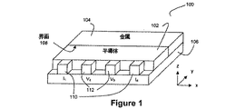
図1は、EMR、EPC、EACおよびEOCのタイプのナノスケールEXXセンサ100についての好ましい構造を示す。図1に図示されるように、ナノセンサ100は、半導体部分102および金属分路部分104を含むハイブリッド半導体/金属デバイスである。半導体102および金属分路部分104は、基板106上に配設される。半導体部分102と金属分路部分104とが共に、半導体/金属界面108を画定する。好ましくは、半導体部分102および金属分路部分104は、図1に図示されるように実質的に同一平面にある。さらに、半導体部分102および金属分路部分104は、基板106のように実質的に平行面内に位置すると好ましい。また、半導体/金属界面108の平面は、基板106の平面に対して実質的に垂直であると好ましい。図1のナノセンサ100の構造は、外部分路化されたファンデルポー(vdP:van der Pauw)プレートと呼ばれる。
FIG. 1 shows a preferred structure for a
半導体部分102は、約1000nmの厚さを有する薄い半導体膜であると好ましい。しかし、例えば約25nmと約2000nmとの間の範囲内の厚さなど、他の厚さの値を使用することもできることを理解されたい。さらに、半導体膜102は、約100nmの長さおよび約50nmの幅を有すると好ましい。しかし、例えば下限がリソグラフィ能力のみによって制約を受ける任意のナノスケール値(現行では約5nmと考えられているが、時の経過および技術の向上によりこの下限はさらに低下し得る)など、半導体膜に関する他の長さおよび幅を使用することが可能であることに留意されたい。本明細書において使用される際に、「厚さ」という語は、図1に図示されるz軸に沿った寸法を指し、「長さ」という語は、図1に図示されるy軸に沿った寸法を指し、「幅」という語は、図1に図示されるx軸に沿った寸法を指す。
The
金属分路104に関する寸法は、厚さが約1000nm、長さが約100nm、幅が約100nmであることが可能である。しかし、(1)例えば約25nmから約2000nmの範囲内の厚さなど、他の厚さの値を使用することが可能である、ならびに(2)例えば上述のように利用可能なリソグラフィ技術によってのみ最小値が制限される任意のナノスケールの長さまたは幅など、他の長さおよび幅を使用することが可能である、ということを理解されたい。また、半導体膜102に対する金属分路104の寸法は、連続的に変化可能であることが予期され、この関係が、デバイスについての充填率を規定することに留意されたい。また、半導体膜102の寸法に対して、分路の幅は、典型的には半導体膜の幅以下であることに留意すべきである。典型的には、分路の厚さは、半導体膜の厚さと同一であるが、分路は、半導体膜よりも薄くてよい(普通は、分路は半導体膜よりも厚くない)。
The dimensions for the
好ましくは、基板106の寸法は、半導体膜および金属分路よりもはるかに大きい。基板106に関する寸法は、厚さが約400μmで、直径が約2インチであると好ましい。しかし、これらの値は、本発明の実施者の設計選択に応じて大幅に変わることが可能であることを理解すべきである。
Preferably, the dimensions of the
また、ナノセンサ100は、2つの電流リード110および2つの電圧リード112を含むと好ましい。これらのリードは、半導体膜102に接触するが、金属分路104には接触しない。また、これらのリードは、図1に図示されるように半導体/金属界面108の反対側の面上で半導体膜102に接触することが好ましい。リードの形状に関しては、2つの電圧リード112は、図1に図示されるように2つの電流リード110の間に配設されると好ましい。さらに、リード間の間隔は、ナノセンサ100の異常磁気抵抗/ピエゾコンダクタンス/音響コンダクタンス/光コンダクタンス効果を最大化するように選択されることが好ましい。
In addition, the
EMRセンサおよびEPCセンサとして図1の構造を使用することは、上記で引用され参照により本明細書に組み込まれる特許および刊行物において説明されるように、当技術において知られている。しかし、それらの動作原理を簡単に繰り返して述べる。図1のハイブリッド半導体/金属デバイス100の4−リード有効抵抗は、Reff=V23/I14であり、ここでIおよびVは、それぞれ電流リード110および電圧リード112を表す。Reffの値は、金属104および半導体102の相対導電率(典型的にはσmetal/σsemiconductor>1000)、界面108の抵抗、ならびに電流リードおよび電圧リードの特定の配置(リード形状)に左右される。ハイブリッド半導体/金属デバイス100が非被摂動状態にある場合に、高導電性金属は、界面108の抵抗が十分に低く、Reffが金属のそれに近いことが可能である条件においては、有効な電流分路として作動する。しかし、磁場、圧力/ひずみまたは温度における変化などの比較的に小さい摂動がハイブリッド半導体/金属デバイス100に加えられる場合には、半導体102のバルク抵抗および/または界面108の著しい抵抗変化が誘発される可能性があり、随伴的に、界面108の間の電流が著しく変化する。これらの誘発される変化は、電流が電流リード110を介してハイブリッド半導体/金属デバイス100に供給される際に電圧リード112からの出力電圧信号により容易に測定することが可能なReffにおける比較的大きな変化として現れる。
The use of the structure of FIG. 1 as an EMR sensor and an EPC sensor is known in the art, as described in the patents and publications cited above and incorporated herein by reference. However, these operating principles will be briefly and repeatedly described. The 4-lead effective resistance of the hybrid semiconductor /
図2は、図1のセンサ100のEACセンサとして使用を示す。EACナノセンサについては、測定可能な電圧応答をもたらす摂動は、音波202である。音響摂動源200からの音波202は、異常ピエゾコンダクタンス効果により測定可能な電圧をもたらす界面108でのひずみを生じさせる。このように、EACセンサは、EPCセンサに非常に類似している。好ましくは、音波202の方向は、概してz軸に沿う(または、半導体膜102および金属分路104の平面に対して垂直である、または界面108の平面と実質的に同一面内にある)と好ましい。
FIG. 2 illustrates use of the
EAC/EPCセンサについては、半導体/金属界面108は、電流に対するショットキー障壁を生成する。界面108の方向に沿った引張(圧縮)ひずみが原子間隔を広げ(狭め)、それにより障壁の高さを高める(低くする)。障壁を通過するトンネル電流は障壁の高さに指数関数的に左右され、このトンネル電流における任意の変化はEAC構造により増幅されるため、小さなひずみが大きな電圧変化/信号をもたらす。本発明者らによる実験により、9/16の充填率により構造が特徴付けられるEPCセンサに対してピエゾコンダクタンスが最大になることが明らかになった。米国特許出願公開第2002/0129087号を参照されたい。
For EAC / EPC sensors, the semiconductor /
本発明の実施において使用することが可能な音響摂動源の例には、走査型超音波顕微鏡(SAM)、合成開口集束技術(SAFT)を使用する超音波エミッタ、フェーズドアレイトランスデューサまたは単一素子集束もしくは非集束超音波トランスデューサを用いる医用画像機器、衝撃波デバイス、中高強度集束超音波アレイ、あるいは細胞および組織中に機械的波動を誘起することが可能な代替源が含まれる。例としては、音響摂動の特徴は、極超短波(UHF)帯の間の周波数(300MHzから3GHz、5μmと500nmとの間の波長に相当)、超高周波(SHF)帯の下方部分の周波数(3GHzから30GHzまで、500nmから50nmまでの波長に相当)が可能である。 Examples of acoustic perturbation sources that can be used in the practice of the present invention include scanning acoustic microscopes (SAMs), ultrasonic emitters using synthetic aperture focusing technology (SAFT), phased array transducers or single element focusing. Alternatively, medical imaging equipment using unfocused ultrasound transducers, shock wave devices, medium to high intensity focused ultrasound arrays, or alternative sources capable of inducing mechanical waves in cells and tissues are included. As an example, acoustic perturbation features include frequencies between the ultra-high frequency (UHF) bands (corresponding to wavelengths between 300 MHz to 3 GHz, 5 μm and 500 nm), frequencies in the lower part of the super-high frequency (SHF) band (3 GHz). To 30 GHz, corresponding to wavelengths from 500 nm to 50 nm).
図3は、図1のセンサ100のEOCセンサとしての使用を示す。EOCナノセンサについては、測定可能な電圧応答をもたらす摂動は、光302である。半導体膜102および金属分路104の露光面に衝突する光摂動源300からの光302は、異常光コンダクタンス効果により測定可能な電圧をもたらす。好ましくは、光302についての伝播方向は、概してz軸に沿う(または半導体膜102および金属分路104の平面に対して垂直である、または界面108の平面と実質的に同一面内にある)。しかし、以下に述べるように、EOCナノセンサのサイズが低下すると、光は、EOCナノセンサが小サイズであることにより、EOCナノセンサをさらに均一に照明する。
FIG. 3 illustrates the use of the
光摂動源300は、レーザ発光デバイスやさらには蛍光発光を伴う細胞(フッ素ベース造影剤の添加により発光されるものなど)などの、任意の発光源であることが可能である。さらに、摂動光は、赤外から紫外範囲におよぶ数百ナノメートルの測定波長を有する電磁放射であることが可能である。
The
図4は、(1)波長476nm、直径10μm、15Kで電力5mWの集束Arイオンレーザビームに露光された場合のマクロスコピックGaAs−In半導体/金属ハイブリッドEOCセンサ100(半導体膜102がGaAsを含み、金属分路104がInを含む)の光応答(上方パネル)、ならびに(2)同一のレーザ放射に対するマクロスコピックベアGaAs(In分路を有さない)の光応答(下方パネル)を示す。図4は、複数の離散走査z位置について、EOCセンサ100のx軸に沿ったレーザビームの走査位置に対する光コンダクタンスを図表化し、ここでx方向およびy方向は、図4の差込み図により特徴付けされる。図4のパネルは、EOCセンサの3つの注目に値する特徴、すなわち(1)出力電圧信号増幅が電圧プローブ112付近でピークに達する(電圧プローブ112の位置に対応するx軸上の位置での電圧応答におけるピークを参照)、(2)電圧応答がベアGaAsに対してよりも分路化されたEOCセンサに対しての方がはるかに大きい(〜500%)(それによりEOC効果を示す)、ならびに(3)レーザの焦点がIn分路の方にz方向(図3のセンサ100においてはy軸方向になる)に移動すると出力電圧信号増幅が低減する、を示す。
4 shows (1) a macroscopic GaAs-In semiconductor / metal hybrid EOC sensor 100 (
これらのEOC効果は、以下のように理解することが可能である。レーザ摂動は、半導体膜102によって吸収され、周囲「暗」密度よりもはるかに大きな非常に高密度の電子正孔対を生成する。電子が、はるかに高い移動度を、したがって正孔よりもはるかに大きな平均自由行程を有するため、電子は、金属分路104によって効率的にグラウンドに短絡され、センサ100の表面上に衝突するレーザビームの中心から径方向に外方に広がる余剰正孔の正電荷領域を残す。この余剰正孔電荷は、レーザビームがX方向に沿ってプローブ112を通過する際に、強調された信号をもたらす、電圧リード112での追加的な電場を生成する。しかし、余剰正電荷の領域が、Z方向(または図3のy軸)に沿って分路104のさらに近くに移動すると、ますます多くの正孔もグラウンドに短絡され、余剰が低減する。これにより、Z方向レーザ衝突の上昇に伴う信号の低下がもたらされる。この低下にさらに寄与するものが、これらの電圧接点からレーザスポットのZ方向距離を有する電圧接点での余剰正孔誘起される電場の低減からもたらされる。分路104がない場合には、電子は、グラウンドに効率的に短絡されることが不可能となり、レーザスポットの領域内の余剰正(正孔)電荷の量が、著しく低下する。
These EOC effects can be understood as follows. Laser perturbations are absorbed by the
図5は、図4のセンサについてのEOC効果の温度依存性を図表化する。GaAsデバイスについては、余剰電子が金属分路104に達し、金属分路104によって短絡されるのに十分な余剰電子の平均自由行程の長さとなるのは低温時であるため、EOC効果は低温で最も際立つ。キャリア平均自由行程は、非温度依存である、正孔については温度に対して反比例的に変動するキャリア移動度に比例する。また、図5の図表は、l/T(Tはサンプル温度°Kである)として変動する関数を有するデータに対する最小二乗適合を示し、それによりEOC効果の温度依存性を示唆する。この分析にもとづき、我々は、EOCセンサについて、直接ギャップであるがナローギャップの半導体(室温での移動度がGaAsの70倍であるInSbなど)および/またはナノスコピック構造体を使用することにより、EOC効果が室温で実現されるはずである、と結論付ける。
FIG. 5 charts the temperature dependence of the EOC effect for the sensor of FIG. For GaAs devices, the surplus electrons reach the
また、出力電圧の任意の熱ドリフトを緩和するために、InSb半導体をSiまたはTeドナーでドープして、飽和(例えば非温度依存)領域における外来キャリア高密化を実現することが可能である。 In order to mitigate any thermal drift of the output voltage, the InSb semiconductor can be doped with Si or Te donor to achieve higher density of foreign carriers in a saturated (eg, non-temperature dependent) region.
また、本発明者らは、EOCセンサのサイズが小さくなると、光摂動源により行われる照明がEOCセンサ上で事実上均一になることが達成されることに注目する。この均一性は、X位置に関する図4の図表と事実上結びつくように作用し、これは、EOCセンサからの電圧応答の強度において著しい低下をもたらす。 The inventors also note that as the size of the EOC sensor is reduced, it is achieved that the illumination provided by the light perturbation source is virtually uniform on the EOC sensor. This uniformity acts in effect in conjunction with the diagram of FIG. 4 regarding the X position, which results in a significant decrease in the strength of the voltage response from the EOC sensor.
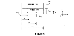
この問題に対する1つの解決策は、x軸に沿ってリード110および/または112を非対称に配置することである。一実施形態においては、このような非対称配置を、x軸に沿って電圧リード112のみを非対称に配置することによって実現することが可能である。図6は、半導体部分102、金属分路部分104ならびに電圧リード1121および1122(それぞれ図3のリードV2およびV3に相当する)を示す例示のEOCセンサ100の上面図を示す。x軸に沿った電圧リード112の位置が、図6に示され、半導体102についてのx軸に沿った全距離が、Xmaxで示される。図6のx軸に沿った一番左の位置を起点として用い、x軸に沿った一番右の位置を値Xmaxとして用いると、電圧リード1121のx軸位置はx1で表され、電圧リード1122のx軸位置はx2で表されることが分かる。電圧リードは、x1およびx2がx2=Xmax−x1となるような値を示す場合には、対称であると呼ばれる。EOCセンサ100の電圧応答を向上させるためには、電圧リード112をx軸に沿って非対称位置に配置することが好ましい。
One solution to this problem is to place the
図3および図6に図示される電圧リード1121と1122との間の電位V23は、電荷への距離にわたる表面電荷密度の積分として計算することが可能である。

実験的に測定されたV23(y)データにσ(y)を適合させることによって、表面電荷密度についての別のモデルを作成することが可能である。Xmax=10mm、x1=3.4mm、x2=6.6mm、Ymax=1mmの値に対して集束されるレーザスポットに露光される縮退ドープGaAsを使用するEOCセンサ100に関してV23を測定した実験においては、様々な値のx1およびx2に対するV23の値は、40μm平方(これはレーザスポットの直径に対応する長さの近似値である)にわたる積分のx限度およびy限度を有するV23について、上述の公式を使用して計算することが可能である。このような実験により得られるV23データは、V23(y)がガウス近似であることを示唆するため、V23についての上述の公式における被積分関数は、y×exp(−y2)の形でなければならない。l/y位置依存性であることを念頭に置くと、実験的適合σ(y)の値は以下のように求めることが可能である。
図7aの図表は、一様電荷密度、固定ysが0.5mm、Ymax/Xmax比が1/10と仮定したEOCセンサ100の計算された電圧出力V23を示す。様々なリード位置x1およびx2が、xy面上に示され、電圧は、縦座標上に示される。この図表においては、電圧応答の対称性が明らかである。この図表においては、最適なリード位置は、(x1、x2)が、(0mm、5mm)および(10mm、5mm)の位置であると確定することが可能であり、これらの位置で電圧応答は最大になる。一方のリードがXmax距離の中間に位置し、他方のリードがXmax距離の両端に位置するこれらの位置は、中間リードが、最小電荷へのアクセスを有する端部上のリードと比較して、最大電荷の最も近くに位置するものとして定性的に理解することが可能である。
Table of FIG. 7a shows a uniform charge density, a fixed y s is 0.5mm, Y max / X max ratio voltage output V 23 calculated the
また、別の実施形態においては、非対称リード配置は、x軸に沿って電流リード112のみを非対称に配置することにより実現することが可能であることに留意されたい。さらに、非対称リード配置は、x軸に沿って電流リード110および電圧リード112の両方を非対称に配置することにより実現することも可能であることに留意されたい。
It should also be noted that in another embodiment, asymmetric lead placement can be achieved by placing only the
均一照明の問題に対する別の解決策は、図8a(上面図)および図8b(側面図)に図示されるように、カバー800を使用して光摂動にさらされるEOCナノセンサの一部分を遮蔽することである。このように、非均一照明は、半導体102および金属分路104の露出面の光の一部による摂動を妨げることによって実現することが可能である。例えば、カバー800を使用して、他の場合には露出される半導体102および金属分路104の面の半分をブロックすることが可能である。カバー800は、カバー800の底面について、絶縁体(例えばSiO2など)の薄膜(例えば20nmなど)層などの材料から形成することが可能であり、カバー800の露出面としての任意の金属からなるさらに厚い層(例えば50nmまたはそれ以上)が後に続く。別の例としては、カバー800は、任意の不透過性絶縁体の単一層(例えば50nm層など)から形成することが可能である。
Another solution to the problem of uniform illumination is to use a
図7bの図表は、一様電荷密度、固定ysが0.5mm、Ymax/Xmax比が1/10と仮定したEOCセンサ100の計算された電圧出力V23を示し、カバー800が、EOCセンサ100の露出面の半分をブロックするために使用される。様々なリード位置x1およびx2が、xy面上に示され、電圧は、縦座標上に示される。分かるように、図7aの図表に見られる減損を伴うことなく、対称リードを使用することが可能である。
Chart of Figure 7b, uniform charge density, fixed y s is 0.5mm, Y max / X max ratio indicates EOC voltage output V 23 the
均一な照明下におけるEOCセンサの電圧応答を上昇させるのに結果有効(result−effective)である別の構造パラメータは、Ymax/Xmax比である。これは、図7cにおける例により理解することが可能である。図7cは、Ymax/Xmax比に対する均一照明されるEOCセンサからの計算された出力電圧の図表を示す。また、図7cは、EOC応答の図表を示し、EOC応答は、ベア半導体センサの出力電圧と比較した、EOCセンサの測定された出力電圧におけるパーセント差として規定される。また、図7cは、Ymax/Xmax比に対するベアデバイスについての電圧応答を示す。 Another structural parameter that is result-effective in increasing the voltage response of the EOC sensor under uniform illumination is the Y max / X max ratio. This can be understood from the example in FIG. FIG. 7c shows a diagram of the calculated output voltage from a uniformly illuminated EOC sensor against the Y max / X max ratio. FIG. 7c also shows a diagram of the EOC response, where the EOC response is defined as a percent difference in the measured output voltage of the EOC sensor compared to the output voltage of the bare semiconductor sensor. FIG. 7c also shows the voltage response for the bare device versus the Y max / X max ratio.
図9は、ナノスケールEECセンサ900についての好ましい構造を示す。図9に図示されるように、ナノセンサ900は、半導体部分902および金属分路部分904を含むハイブリッド半導体/金属デバイスである。金属分路部分904は、半導体部分902の表面上に配設され、半導体部分902は、金属分路部分902と基板906との間に挟まれるように、基板906の表面上に配設される。図9に図示されるように、金属分路部分904、半導体部分902および基板部分906は、実質的に平行面内に位置すると好ましい。金属分路部分904と半導体部分906との接触部分が共に、半導体/金属界面908を画定する。したがって、図1のナノセンサ100とは異なり、ナノセンサ900の半導体/金属界面908の平面は、金属分路/半導体/基板の平面と実質的に平行である。
FIG. 9 shows a preferred structure for the
半導体部分902は、約1000nmの厚さを有する薄い半導体膜であると好ましい。しかし、例えば約25nmと約2000nmとの間の範囲内の厚さなど、他の厚さの値を使用することが可能であり、厚さの値は、熱雑音低下および信号対雑音比における改善のために入力抵抗を低減させるように選択されることを理解されたい。さらに、半導体膜902は、長さが約100nmであり、幅が約50nmであると好ましい。しかし、例えば下限がリソグラフィ能力のみによって制約を受けるナノスケールの長さおよび幅など、半導体膜902の他のナノスケールの長さおよび幅の値を使用することが可能であることに留意されたい。
The
金属分路904についての寸法は、厚さが約1000nm、長さが約100nm、幅が約50nmであると好ましい。EECナノセンサについては、金属分路904の幅および長さは、半導体膜902の幅および長さ以下であり、それを超過しないことが好ましい。しかし、やはり、他の厚さ(例えば、約25nmから約2000nmの範囲内の任意の値などで、厚さの値は、熱雑音低下および信号対雑音比における改善のために入力抵抗を低減させるように選択される)を使用することが可能であることを理解されたい。また、分路のナノスケールの長さおよび幅も、半導体膜の長さおよび幅を超過しないように選択される他の値であることが可能であり、下限はリソグラフィ能力のみによって制約を受ける。
The dimensions for
好ましくは、基板906の寸法は、半導体膜902の寸法を支持するように適切にサイズ設定され、そのため典型的には、基板906は、半導体膜および金属分路よりもはるかに大きい。基板906についての例示の寸法は、好ましくは厚さが約400μmであり、直径が約2インチである。しかし、他の寸法を使用することが可能であることを理解されたい。
Preferably, the dimensions of the
また、ナノセンサ900は、2つの電流リード910および2つの電圧リード912を含むと好ましい。これらのリードは、半導体膜902に接触するが、金属分路904には接触しない。また、これらのリードは、図9に図示されるように、半導体膜902のxz厚さに沿った表面上で半導体膜902に接触することが好ましい。リードの形状については、2つの電圧リード912は、図9に図示されるように、2つの電流リード910の間に配設されると好ましい。さらに、リード間の間隔は、ナノセンサ900の異常電子コンダクタンス効果を最大化させるように選択されることが好ましい。
In addition, the
図9のEECナノセンサについては、外部摂動電場がない場合には、電流リードI1で入り電流リードI4から出るバイアス電流は、半導体膜902よりもはるかに高い導電性のため、金属分路904を主に通り流れる。しかし、金属分路904にアクセスするためには、この電流は、材料の適切な選択により、界面908でショットキー障壁をトンネル通過しなければならない。このトンネル電流は、障壁に印加される外部バイアスに対して指数関数的に変動する。したがって、摂動電場が界面908(EECセンサの表面上に配設される癌細胞の表面電荷など)に衝突すると、次いで摂動電荷は、界面908に対して垂直になる。この摂動場は、金属分路904上の表面電荷の再分布を生じさせ、ショットキー障壁に印加されるバイアス場をもたらす。結果的に得られるトンネル電流の指数関数的変化は、半導体902と金属分路904との間の電流の再配分を生じさせ、これは、電圧リード912間で測定される電圧における大きな検出可能な変化をもたらす。
For the EEC nanosensor of FIG. 9, in the absence of an external perturbation electric field, the bias current entering at current lead I 1 and exiting from current lead I 4 is much higher conductivity than
本発明者らは、以下のように癌細胞から期待することが可能な電場の大きさを推定した。体内の正常な細胞は負の電荷を有することが、一般的には主張され、−100から−10mVの間の値(これは電荷に対する正確な単位を有さない)が、その文献中で挙げられる。これらの電圧値は、電気泳動測定を使用して求められ、電気泳動測定は、実際の細胞電荷に間接的に関連付けられるにすぎない。しばしば、これらの「電荷」測定は、Zeta−Sizerなどのターンキーデバイスを使用して行われ、Zeta−Sizerは、(緩衝溶液中に懸濁している)電場中の帯電粒子のドリフト速度を測定するために散乱するレーザ光を使用することにより作動する。直接測定される量は、
v=μE
により与えられる速度vであり、ここでEは印加される場(典型値はΕ〜10−1V/m)であり、μは電気泳動度であり、導き出される量は、帯電粒子の特性に左右される。細胞のサイズに近いサイズを有する粒子については、
μ=εrε0ζ/η
(Smoluchowskiの公式)となり、ここでεrは比誘電率であり、ηは粘度であり、ε0は真空内の誘電率であり、ζはZeta電位である。典型的な測定値については、ζ〜10−2から10−1Vであり、η〜10−3Pasであり、εr〜80であり、これはμ〜0.7−7.0×10⁻⁸m2s−1V−1を示唆し、これは、典型的な場であるE〜10−1V/mにおいては、
v=μE=(0.7×10⁻⁸m2s−1V−1から7.0×10⁻⁸m2s−1V−1)×(10−1v/m)=0.7×10−9ms−1から7.0×10−9ms−1
を示唆する。粒子が小さいものと仮定すると、粒子が受ける電気的な力Fは、
F=E×q
であり、ここでqは粒子上の全電荷である。これは、半径がRで、速度vで移動する小球状粒子については、
F=6πηRv
により与えられる懸濁化剤の粘性抵抗により平衡され、これは乱流を防ぐのに十分な低さである。典型的な細胞径であるR〜10−5mを条件とし、vおよびηについては上記で挙げた典型的な値を使用すると、
F〜6πηRv=6π×10−3Pas×10−5m×0.7−7.0×10⁻⁹m/s=1.3−13×10−16N
となる。この値を上述のF=Eqに挿入し、典型的な値であるE〜10−1V/mを使用することにより、
F:(1.3×10⁻¹⁶Nから1.3×10⁻¹⁵N)≒10−1(V/m)xq
が与えられ、これは、q=1.3×10⁻¹⁵から13×10−15クーロンとしてとして解かれる。この電荷が細胞の表面上にあると仮定した場合には、これは、100V/cmから1000V/cmのオーダの標準電場を生成する。本発明者らは、この範囲内の場は、金属分路と出力電流リードとの間に0.5Vの順方向バイアス電圧が印加されるナノスケールEECセンサ900において、27から−270μVの出力電圧を生成すると推定する。したがって、半導体/金属界面908で表面電荷誘起されるバイアス場は、EECセンサの電圧応答において容易に検出可能であるはずである。
The present inventors estimated the magnitude of the electric field that can be expected from cancer cells as follows. It is generally claimed that normal cells in the body have a negative charge, and values between -100 and -10 mV (which do not have the correct unit for charge) are listed in the literature. It is done. These voltage values are determined using electrophoretic measurements, which are only indirectly related to the actual cell charge. Often, these “charge” measurements are made using a turnkey device such as Zeta-Sizer, which measures the drift velocity of charged particles in an electric field (suspended in a buffer solution). It works by using scattered laser light to do so. The quantity directly measured is
v = μE
Where E is the applied field (typically Ε-10 -1 V / m), μ is the electrophoretic mobility, and the derived amount depends on the properties of the charged particles. It depends. For particles with a size close to the size of the cell,
μ = ε r ε 0 ζ / η
Where ε r is the relative permittivity, η is the viscosity, ε 0 is the permittivity in vacuum, and ζ is the Zeta potential. For typical measurements, ζ 10 −2 to 10 −1 V, η 10 −3 Pas, and ε r -80, which are μ to 0.7-7.0 × 10 −8 m 2 s −1 V −1 , which is typical for E-10 −1 V / m,
v = μE = (0.7 × 10 −8 m 2 s −1 V −1 to 7.0 × 10 −8 m 2 s −1 V −1 ) × (10 −1 v / m) = 0.7 × 10 −9 ms −1 to 7.0 × 10 −9 ms −1
Suggest. Assuming that the particle is small, the electrical force F experienced by the particle is
F = E × q
Where q is the total charge on the particle. This is for small spherical particles with radius R and moving at speed v
F = 6πηRv
Is balanced by the viscous resistance of the suspending agent given by, which is low enough to prevent turbulence. Subject to a typical cell diameter of R-10 −5 m, and using the typical values listed above for v and η,
F to 6πηRv = 6π × 10 −3 Pas × 10 −5 m × 0.7−7.0 × 10 −9 m / s = 1.13 × 13 × 10 −16 N
It becomes. By inserting this value into F = Eq above and using a typical value of E-10 −1 V / m,
F: (1.3 × 10 −16 N to 1.3 × 10 −15 N) ≈10 −1 (V / m) × q
Which can be solved as q = 1.3 × 10 −15 to 13 × 10 −15 coulombs. Assuming this charge is on the surface of the cell, this produces a standard electric field on the order of 100 V / cm to 1000 V / cm. The inventors have found that a field within this range is an output voltage of 27 to -270 μV in a
さらに、EECナノセンサのショットキー障壁が、半導体/金属界面908の化学不純物により有害的に摂動される場合には、本発明者らは、この障壁に順方向バイアス電圧を印加することがこの問題を緩和するはずであると考える。 Furthermore, if the Schottky barrier of the EEC nanosensor is detrimentally perturbed by chemical impurities at the semiconductor / metal interface 908, the inventors have addressed this problem by applying a forward bias voltage to the barrier. I think it should ease.
図10は、図10の差込み図中に示されるように、GaAsとInとの間にショットキー障壁界面を有するEECセンサ900について水平構造体の、測定された電流−電圧図表を示す。このEECセンサの寸法は、それぞれx、yおよびz軸について、60μm×30μm×50nmであった。この図表より、0−0.5Vの範囲内の順方向バイアス(正)電圧では電流の指数関数的上昇があり、この電流は約−1.5Vまでの逆方向バイアス範囲においてはゼロであると指摘することが可能である。より高い逆方向バイアスでは、電流リークが図10に示されるように生じる。
FIG. 10 shows a measured current-voltage diagram of a horizontal structure for an
図11は、図11の差込み図中に図示される円形EECセンサの測定されたEEC特性を示す。これらのEEC測定は、図11に示されるように、構造充填率であるα=r/R(図11の差込み図を参照)と、−1050V/cmから+450V/cmの範囲内の場に対するショットキー障壁への直接順方向および逆方向バイアスとに関して行われる。既知の全電荷である〜1×10−15クーロンによる癌細胞の表面での場の推定値は、102−105V/cmの範囲内となることを指摘することが可能である。この関連で、EEC効果の定量測度として、EEC効果を
図11において分かるように、EECは、順方向および逆方向の両バイアス方向において充填率により大きく左右され、増加し、順方向における飽和に関して50%を超過する値に達する。ショットキー障壁の特性を調整するためにSiで半導体902を選択的にドープすることにより、EECセンサの性能のさらなる改善を見込むことが可能である。
As can be seen in FIG. 11, the EEC is highly dependent on the fill factor in both the forward and reverse bias directions, increases and reaches a value exceeding 50% for saturation in the forward direction. By selectively doping the
これらのナノスケールEXXセンサに関して、半導体材料、金属分路材料および基板材料の様々な組合せを選択することが可能である。 For these nanoscale EXX sensors, various combinations of semiconductor materials, metal shunt materials, and substrate materials can be selected.
EMRナノセンサについては、適切な半導体材料の例としては、InSb、InAsおよびHg1−xCdxTeが含まれ、または任意のナローギャップ半導体が含まれ、適切な金属の例は、Auまたは任意の良質の非磁性金属である。EMRナノセンサについての適切な基板材料の例としては、高絶縁性ワイドギャップ半導体または絶縁体が含まれ、好ましい材料は、特性およびコストの両方において有利であるためGaAsである。 For EMR nanosensors, examples of suitable semiconductor materials include InSb, InAs and Hg 1-x Cd x Te, or any narrow gap semiconductor, examples of suitable metals are Au or any It is a good quality non-magnetic metal. Examples of suitable substrate materials for EMR nanosensors include highly insulating wide gap semiconductors or insulators, with GaAs being the preferred material because it is advantageous in both properties and cost.
EPCナノセンサおよびEACナノセンサについては、適切な半導体材料の例としては、GaAs、InAsまたは他のIII−V族半導体が含まれ、適切な金属の例としては、Auまたは任意の高導電性金属が含まれる。EPC/EACナノセンサ用の基板材料に関しては、基板材料の選択肢は、センサに対する摂動のタイプにもとづいて様々であってよい。例えば、高周波で大振幅の音響信号を検出するためにはGaAsなどの「剛性」基板を選択することが可能であり、他方では小振幅の低周波信号に対してはGaSbがより望ましい選択肢となる。また、信号選択性は、基板の寸法または構造特性の賢明な設計により調整することが可能であり、例えば、長く薄く狭い基板は、弱い音響摂動に対して線形的に応答するが、他方で厚い基板は、より強い音響摂動に対してより線形的に応答する。基板および半導体膜が共にGaAs材料から構成される場合には、半導体膜において使用されるGaAsは、基板において使用されるGaAsとは異なる不純物濃度を有するべきである。 For EPC and EAC nanosensors, examples of suitable semiconductor materials include GaAs, InAs or other group III-V semiconductors, and examples of suitable metals include Au or any highly conductive metal It is. With respect to substrate materials for EPC / EAC nanosensors, the substrate material options may vary based on the type of perturbation for the sensor. For example, a “rigid” substrate such as GaAs can be selected to detect high amplitude and large amplitude acoustic signals, while GaSb is a more desirable option for small amplitude low frequency signals. . Signal selectivity can also be tuned by judicious design of substrate dimensions or structural characteristics, for example, long thin thin substrates respond linearly to weak acoustic perturbations but thick on the other hand The substrate responds more linearly to stronger acoustic perturbations. If both the substrate and the semiconductor film are composed of GaAs material, the GaAs used in the semiconductor film should have a different impurity concentration than the GaAs used in the substrate.
EOCナノセンサについては、適切な半導体材料の例としては、GaAs、InSbおよび他の直接ギャップ半導体が含まれ、適切な金属の例としては、Inまたは任意の高導電性金属が含まれる。適切な基板材料の例としては、GaAsおよび他の高抵抗材料が含まれる。基板および半導体膜が共にGaAs材料から構成される場合には、やはり、半導体膜において使用されるGaAsは、基板において使用されるGaAsとは異なる不純物濃度を有するべきである。 For EOC nanosensors, examples of suitable semiconductor materials include GaAs, InSb, and other direct gap semiconductors, and examples of suitable metals include In or any highly conductive metal. Examples of suitable substrate materials include GaAs and other high resistance materials. If both the substrate and the semiconductor film are made of GaAs material, again, the GaAs used in the semiconductor film should have a different impurity concentration than the GaAs used in the substrate.
EECナノセンサについては、適切な半導体材料の例としては、GaAsおよび他のドープ半導体が含まれ、適切な金属の例としては、Auまたは任意の他の高導電性金属が含まれる。適切な基板材料の例としては、GaAsまたは任意の適切な絶縁性の基板材料が含まれる。基板および半導体膜が共にGaAs材料から構成される場合には、やはり、半導体膜において使用されるGaAsは、基板において使用されるGaAsとは異なる不純物濃度を有するべきである。 For EEC nanosensors, examples of suitable semiconductor materials include GaAs and other doped semiconductors, and examples of suitable metals include Au or any other highly conductive metal. Examples of suitable substrate materials include GaAs or any suitable insulating substrate material. If both the substrate and the semiconductor film are made of GaAs material, again, the GaAs used in the semiconductor film should have a different impurity concentration than the GaAs used in the substrate.
EXXナノセンサへの電流の供給に関して、適切なバイアス電流は、用途および実際のEXXセンサのタイプに応じて、マイクロアンペアまたはミリアンペアの範囲内であることが好ましい。 For supplying current to the EXX nanosensor, a suitable bias current is preferably in the microampere or milliamp range, depending on the application and the actual type of EXX sensor.
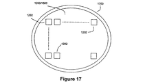
図1〜図9に関連して上述されたナノセンサは、図12aおよび図12bに図示される複数のナノスケールEXXセンサ1202のN×Mアレイ1200を生成するように組み合わせることが可能である。NおよびMの値は、本発明の実施者により、ナノスケールEXXセンサの使用意図にもとづく設計選択のとおりに選択することが可能である(例えば、4×4、16×16、2×20、64×64などで、上の値は製造能力のみによって制約を受ける)。例えば、本発明者らは、現行のデジタルディスプレイ技術から判断されるナノセンサマトリクス寸法は、640×480、800×600、1024×768、1600×1200、2048×1536および3200×2400も可能であると予期する。これらのナノスケールEXXセンサ1202は、SiO2基板などのアレイ基板1204上に配設することが可能である。基板1204の好ましい厚さは、約400μmであるが、他の厚さを使用することが可能である。個々のナノスケールEXXセンサの電圧リードおよび電流リードは、説明の容易化のために図12aおよび図12bにおいては図示されないことに留意されたい。また、特に多数のナノセンサを有するアレイ(図13を参照)について、アレイ1200中のナノセンサ1202のマトリクスからアドレス指定する行/列ピンアウト配列についてのビア設計を使用することが可能であることに留意されたい。図13に図示されるアレイ構造については、EXXセンサ1202についての4−リードのそれぞれが、個別にアドレス指定可能なものであることが可能であり、それによりn×nアレイに対して4n2のピンアウトがもたらされる。さらに、これらのリードは、選択的に組み合わせて、n×nアレイに対して3n+1のピンアウトへの削減をもたらすことが可能である。
The nanosensors described above in connection with FIGS. 1-9 can be combined to produce an N ×
また、個々のEXXセンサが基板1204と同一の材料からなる基板106を有するように設計される場合には、アレイ1200上に配置されるEXXセンサ1202は、この場合には基板1204の材料が適切な基板として機能することが可能であるため、基板106を含む必要がないことに留意されたい。しかし、基板材料が異種のものである場合には、個々のEXXセンサ1202は、それら自体の基板106を含むことが好ましい(例えば、EXXセンサ1202がGaAs基板106を有し、他方でアレイ1200がSiO2基板1204を有する場合)。好ましくは、アレイ1200は、EXXセンサ1202間に狭い間隔を呈する。例えば、約50nmから約1000nmの範囲内となる間隔値を使用することが可能である。
In addition, when each EXX sensor is designed to have the
EXXセンサのタイプ(または複数のタイプ)の選択および、EXXセンサのタイプ(または複数のタイプ)のアレイ1200上での配置は、大きく変更可能であることが可能である。例えばアレイ1200は、単一タイプのナノスケールEXXセンサ1202のみを含むことが可能である(例えば、EACセンサのみのアレイ、EOCセンサのみのアレイ、EECセンサのみのアレイなど)。また、アレイ1200は、ナノスケールEMR/EPC/EAC/EOC/EECセンサ1202の任意の組合せなど、複数の様々なタイプのナノスケールEXXセンサを含むことが可能である。複数の様々なタイプのEXXナノセンサ(EAC/EOC/EECナノセンサなど)を1つのアレイに組み込むことにより、LSCのように、電荷および蛍光イメージングの出力にもとづいて細胞の予期される疑問についてのHCSを実施することが可能なスクリーニングシステムが提供される。しかし、音響サブシステムの分解能は、光学顕微鏡検査から得られるもの以上であり、デジタル化された超音波波形の時間軸が、現行で入手可能な臨床用超音波システムを用いての器官構造のイメージングに非常に類似する、分散関係によりイメージングされる細胞への距離にマッピングすることが可能な情報を含むため、容積データをさらに提示する(すなわち一度に単一の焦点面に限定されない)。このタイプの計装は、ナノスケール音響顕微鏡検査にもとづく容積データの同時取得、高価な高強度光源を必ずしも必要としない現行の光学顕微鏡検査よりも高い分解能、電気泳動技術に固有の複雑さおよび曖昧さを伴わない高精度および高分解能表面電荷測定、ならびに高分解能で低ノイズの蛍光イメージングなどの、現行のサイトメトリ/顕微鏡検査器具では得ることのできない複数の利点を提供する。
The selection of the EXX sensor type (or types) and the placement of the EXX sensor type (or types) on the
また、アレイ1200は、図14aに図示されるように、複数のピクセル1400にさらに細分化されるものとして見なすことが可能であることに留意されたい。各ピクセル1400は、1つまたは複数のナノセンサ1202を含むことが可能である。例えば、図14(b)に図示されるように、ピクセル1400は、4つのナノセンサのタイプ「A」「B」「C」「D」(ここで、タイプ「A」はEOCナノセンサに対応し、タイプ「B」はEPCナノセンサに対応し、タイプ「C」はEECナノセンサに対応し、タイプ「D」はEMRナノセンサに対応することが可能である)などの複数の様々なタイプのナノセンサ1202を含むことが可能である。ピクセル1400内の様々なタイプのナノセンサのこのようなグループは、ナノセンサの電圧応答に対して信号加算平均技術を使用することにより、アレイ1200の感度を向上させるのに有効となることが可能である。
It should also be noted that the
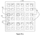
同様に、合成ピクセルを形成するために、ピクセル1400またはその一部分を他のピクセル1400またはその一部分と共にグループ化することが可能であることに留意されたい。例えば、図15aは、図14bに図示される配置の4つのピクセル1400のグループ化により形成される合成ピクセル1500を示す。さらに、合成ピクセル1500は、1つのタイプのナノセンサのみから形成することが可能である(例えば、図15(a)において太字表記により示されるような、4つのピクセル1400内の「A」タイプナノセンサのみなど)。やはり、合成ピクセルのこのような配置は、信号加算平均技術の使用により感度を向上させるのに有効となることが可能である。
Similarly, it should be noted that
図15bは、直線状に配置される同一タイプの複数のナノセンサから形成され、複数のピクセル1400の長さ(例えば合成ピクセル1502内に太字で示される「A」タイプのナノセンサなど)を有する合成ピクセル1502の一例を示す。また、図15(b)は、合成ピクセル1502に対して直角に直線状に配置される同一タイプの複数のナノセンサから形成され、複数のピクセル1400の長さを有する合成ピクセル1504の一例を示す。合成ピクセル1502および1504などの配置された合成ピクセルは、光信号の位相型イメージング、偏向された光の偏光、または使用されるナノセンサのタイプに応じた様々な音響モード(例えばシアープレートモード、横プレートモード、種々のプレートモードなど)の検出に有効であることが可能である。
FIG. 15b is a composite pixel formed from a plurality of nanosensors of the same type arranged in a straight line and having a plurality of
1つまたは複数の細胞などの対象物が、EXXセンサ1202の露出面上のアレイ1200に接触するように置かれ、アレイのEXXセンサ1202が、摂動されると、種々のEXXセンサ1202の電圧応答は、信号処理装置(図示せず)を含む受信器電子機器により、測定し、デジタル化し、保存し、および処理することが可能である。次いで、電圧応答の収集されたものが、EXXセンサ間の空間関係にもとづいて選択的にピクセル化されて、対象物の1つまたは複数の特性を示す対象物の画像を生成することが可能となる。単一モード画像およびマルチモーダルパラメータ化画像は共に、種々のタイプのナノセンサからの出力を重ね合わせ組み合わせることによって生成することが可能である。アレイのEXXセンサがナノスケールであるため、結果的に得られる画像もまたナノスケールの分解能を呈する。さらに、各ナノスケールEXXセンサ1202は、データ取得速度(単位時間当たりの対象物の所与の区域のフレームのイメージング)を高めることを可能にするように、受信器電子機器による個別にアドレス指定可能であることが可能である。また、細胞の成長能力およびアレイ表面への付着能力を強化するために、1つまたは複数の細胞がアレイに接触するアレイの露出面を、フィブロネクチン、ビトロネクチン、コラーゲンなどのタンパク質、あるいはポリ−L−リジンまたはシランなどのタンパク質類似物質で被覆することが可能であることに留意されたい。
When an object, such as one or more cells, is placed in contact with the
例えば、アレイ1200が複数のEACセンサおよびEECセンサ1202から構成される場合には、細胞がこのアレイの上に配置された後に、アレイは、ナノスケール分解能を有する細胞の超音波画像を生成することが可能なEACセンサから電圧応答を取得するために、音波により摂動させることが可能である。同時に、アレイ1202上のEECセンサは、細胞自体からの表面電荷によって摂動して、ナノスケール分解能を有し細胞上の電荷の空間分布を示す画像を生成することが可能なEECセンサからの電圧応答を生成することが可能である。さらに、細胞からの表面電荷はEACセンサを摂動させる傾向がないため、ならびに音波はEECセンサを摂動させる傾向がないため、EECセンサとEACセンサとの間のクロストークを最小化させることが可能であり、細胞の複数の特性の画像を同時に生成することが可能である。
For example, if the
しかし、アレイ1200がEAC/EPCセンサおよびEOCセンサを共に含む場合には、クロストークが生じ、光摂動によってEACセンサにおいて望ましくない電圧応答が生じ、音響摂動によってEOCセンサにおいて望ましくない電圧応答が生じる可能性があることに留意されたい。このようなクロストークの効果を低減させるために、連続的に加えられる摂動とそれにもとづき摂動が加えられるナノセンサの選択的疑問とを有するEOCセンサとは異なる時に、EACセンサを選択的に摂動させることが可能である。細胞自体が光摂動源である場合には(おそらく細胞による自発的な発光ではなく、むしろ外部光場への露光後の発光)、細胞内に存在する燐光成分がある場合には、クロストークは低減される可能性がある。そのような場合には、信号処理技術(ロックイン増幅、デジタルロックイン、パルスゲーティング、時間相関など)を使用して、EAC信号とEOC信号とを区別することが可能である。EOCに関しては、吸光度および反射率の場合に、細胞の応答は基本的に瞬時であり、例えば、吸収信号および反射信号が、これに関連する時間スケールにおける位相遅延が基本的にない、入射光信号と同一のプロファイルを基本的に有する。そのため、EPCからEOCの吸光または反射のいずれかの一時的な分離は、問題とはならないはずである。蛍光の場合には、EOC信号は、細胞の蛍光寿命に左右される。これがマイクロ秒以下の範囲内またはそれより短い場合には、蛍光信号は、吸光および伝達EOCと同一の方法により処理することが可能である。ミリ秒以上の長さのオーダである場合には、(実質的にDCの)EOCベースライン変更をEPC信号に加えることが可能であるが、ベースラインを上回る信号は依然として容易に認識可能であるはずである。この結果は、長寿命蛍光が存在する場合のEPC信号の検出のために適用可能であるが、より短時間の音響信号と同期させるように検出システムをゲーティングすることにより、ベースライン変更を拒否させることが可能である。また、信号選択を実現するためには、ハードウェア方法がある。厚い領域および薄い領域を有する基板を製造し、厚い領域上にEOCセンサを、薄い領域上にEPCセンサを配設することにより、EOC領域が、音響信号を、それらの一時的特性にかかわらず受信しないようにすることが可能である。同様に、EPCセンサ上にのみ、薄いが光不透過性の表面膜を配設することにより、EPCセンサは、いかなる光信号も、それらの一時的特性に関わらず受信しないようにすることが可能である。
However, if the
EXXセンサ1202に対する摂動(または複数の摂動)の源は、上に説明したような1つまたは複数の外部摂動源、対象物自体(特にEOCナノセンサおよびEECナノセンサについて)または、アレイに組み込まれる摂動源が可能である。例えば、近接場走査型光学顕微鏡(NSOM)などのレーザ源は、SAFT技術を使用して、光子場を、NSOMが装着/構成されている走査トンネル顕微鏡(STM)の圧電式X移動制御およびY移動制御装置によるアレイ間のX方向およびY方向への走査/駆動が可能な小サイズ(1ミクロン以下およびアレイ上のEXXセンサ間の間隔未満のオーダ)に空間的に局在化することが可能である。STMは、任意のEACナノセンサを摂動するために使用することが可能であり、NSOMは、任意のEOCナノセンサを摂動するために使用することが可能である。NSOMは、適切なレーザから、テーパ形状の金属被覆された光ファイバの端部のミクロン未満のサイズの開口を介して光を誘導する。近接場方法は、光子場に、可視領域内の500nmの小ささの側方局在化を与えることが可能である。さらに、EECナノセンサを摂動するために空間局在化される場は、STMスキャナにテーパ状金属チップを取り付け、チップと基板1204上の金属被覆された裏面との間に既知の電圧を印加することによって得ることが可能である。レーザ摂動および電場摂動の両方については、印加される場の空間分解能は、センサアレイの表面へのぴったりとした近接を維持することに左右される。このような近接は、STM(誘導)チップからの信号によるSTMのZ移動のフィードバック制御により維持することが可能である。
The source of perturbation (or perturbations) for
また、アレイのEXXセンサはそれぞれ、アレイのEXXセンサの全てが同一の電流を受けないような態様で、固有のバイアス電流を受けることが可能である、ということは注目に値する。例えば、アレイのEXXセンサ1−10が電流Aを受け、アレイのEXXセンサ11−20が電流Bを受けてよい。他の例としては、20のそれぞれ異なる電流を、アレイの20個のEXXセンサに供給することも可能である。 It is also noteworthy that each of the array EXX sensors can receive a unique bias current in such a manner that not all of the array EXX sensors receive the same current. For example, the array EXX sensors 1-10 may receive current A and the array EXX sensors 11-20 receive current B. As another example, 20 different currents can be supplied to the 20 EXX sensors of the array.
図16aおよび図16bは、本発明のための別のアレイの実施形態を示し、摂動源が、アレイ1600に組み込まれる。アレイ1600は、アレイのEAC/EPCナノセンサ1202を摂動するための音波を生成する役割を果たす組込み型PZTトランスデューサ1604を含む。アレイ1200と同様に、個々のナノスケールEXXセンサ1202の電圧リードおよび電流リードは、説明の容易化のために図16aおよび図16bには図示されない。しかし、ナノセンサリードへの基板1204上に配設される電気トレースのためにグラウンド−信号−グラウンド(GSG)配線構造を使用して、信号周波数のUHFおよびSHF範囲内の特性を向上させることが可能であることに留意されたい。アレイ1600に関しては、EXXセンサ1202および基板1204は、図12aおよび図12bに関連して上で説明したように配置することが可能である。しかし、PZTトランスデューサ1604が存在するため、ナノスケールEXXセンサ1202の少なくともいくつかがEPC/EACセンサであることが好ましい。また、アレイ1600は、基板1204の平面に対して実質的に平行な平面内に位置するトランスデューサ基材1608を含むと好ましい。基材1608についての材料および厚さは、圧電式薄膜トランスデューサ1604の音響インピーダンスに類似的に合致し、(基材に当てられる音波を減衰させ)、望ましくない複数の残響共鳴効果を最小限に抑え、(さらに短い時間のパルスおよびさらに高い軸方向分解能に対応する)デバイスの有効周波数帯域幅を効果的に広げるように薄膜1604の「Qを損なう」のに十分な損失の多さの音響インピーダンスを有するように選択されると好ましい。基材1608の一例は、粉砕されたタングステン粒子を含むエポキシ樹脂であることが可能である。しかし、上述のような他の基材を使用してよいことに留意されたい。さらに、広帯域幅トランスデューサは(MHz範囲ではなく)GHz範囲になるため、本発明者らは、本明細書において、基材1608の選択が性能にあまり影響を与えないことがあると考える。
FIGS. 16 a and 16 b show another array embodiment for the present invention, in which a perturbation source is incorporated into the
基板1204と基材1608との間に配設されるのは、グラウンド導体1602および高電圧(hot)導体1606に接触するマクロスケール圧電式トランスデューサ1604である。また、マクロスケール圧電式トランスデューサ1604は、基板1204の平面と実質的に平行な平面内に位置すると好ましい。導体1602および1606を通る電流により圧電式トランスデューサ1604を駆動することによって、圧電式トランスデューサは、平面が基板1204の平面に対して実質的に平行であり、伝播方向が基板1204の平面に対して実質的に垂直な広帯域幅音響平面波を発する(アレイのEPC/EACナノセンサの半導体/金属界面108の平面と同一平面における誘導による)。この広帯域幅音響平面波は、EPC/EACナノセンサに対する摂動の役割を果たす。圧電式トランスデューサ1604は、薄膜多結晶または単結晶の灰チタン石セラミック材料(例えば、PZT(チタン酸ジルコニウム酸鉛)および、PNZT(ニオブドープPZT)、PLZT(ランタンドープPZT)、PMN−ZT(マグネシウムニオブ酸塩ドープPZT)などのドープ誘導体など)、あるいはポリマー材料(例えばPVDF(ポリビニリデンジフルオライド)など)などの薄膜圧電式トランスデューサ材料から形成することが可能であり、所望の範囲に周波数応答を調整するように約20nmと約2000nmとの間の厚さを呈することが可能である。しかし、他の材料および厚さを使用することが可能であることに留意されたい。広帯域幅音響平面波の周波数は、GHz範囲内(例えば約1−5GHzなど)であることが可能であるが、他の周波数値を使用することが可能である。
Disposed between the
マクロスケールPZTトランスデューサ1604により生成される広帯域幅平面波は、後方散乱される超音波から再構築される画像の品質を改善する役割を果たし、アレイ1600は、ナノスケール音響トランスミッタを使用して得ることが困難な圧力レベルでイメージングされる対象物の照射(insonification)を可能にする。さらに、伝送素子および受信素子(トランスデューサ1604およびナノセンサ1202のそれぞれ)を分離させることにより、受信電子機器(図示せず)は、大幅に簡素化されて、伝送に関してより高い駆動レベルが可能となり、信号受信のSNRおよび帯域幅の両面を改善することが可能となる。さらに、伝送素子および受信素子を共に単一のアレイに組み込むことにより、高価なSAMなどの外部音響摂動源の必要性を回避することが可能となる。
The broadband plane wave generated by the macroscale PZT transducer 1604 serves to improve the quality of the image reconstructed from the backscattered ultrasound, and the
集積アレイ1600またはアレイ1200は、大量生産することが可能であって、細胞培養皿1700の底部中に組み込むことが可能な廉価な(さらに使い捨て自在な)イメージングデバイスをもたらし(図17を参照)、それにより多数のまたは単一の細胞を音響的にイメージングし、癌、心臓病、炎症性疾患などの疾病の治療を目的とする治療薬の安全性および効能のモニタリングを容易にするデータを継続的に供給することを可能にする。
The
図18は、本発明によるイメージングアレイの別の実施形態を示す。図18は、多重素子ピッチ−キャッチアレイ1800を示す。アレイ1800は、20μm離間する対向対1802の線形構成となるように均等に離間される64対の矩形圧電式(例えばPZTまたは、上述されるものなどの他の圧電式材料)素子1810を含む。ベース1806およびサポート1804が、互いに対向するPZT素子1810の対1802を保持する。また、PZT素子に電力を供給するための駆動電子機器(図示せず)が、アレイ1800内に含まれる。圧電式素子についての例示の寸法は、高さ6.0μm、厚さ300nm、幅250nm、および素子間隔50nm(素子ピッチ300nmに対して、全64素子では全アジマス19.2μm)である。しかし、他の寸法を使用することが可能であり、ゾルゲル蒸着を、ナノスケールPZT素子を製造するための技術として使用することが可能である。
FIG. 18 shows another embodiment of an imaging array according to the present invention. FIG. 18 shows a multi-element pitch-
64個のPZT素子1810(図18の下部の正面図中に示される)は、対向側のパートナーとの20μmのギャップの間を伝播する超音波パルスを生成するように構成され、対向側のパートナーは、受信器として機能する。パルス/エコーモードにおいては、対向側のアレイ上の64個のPZT素子は、反射体として作用する。アレイ1800によりイメージングされる対象物は、対向対1802の間に配置することが可能であり、超音波パルスは、対象物の超音波画像を再構築することが可能な超音波データを生成するために使用することが可能である。
Sixty-four PZT elements 1810 (shown in the lower front view of FIG. 18) are configured to generate ultrasonic pulses that propagate between a 20 μm gap with the opposing partner, and the opposing partner Functions as a receiver. In the pulse / echo mode, the 64 PZT elements on the opposing array act as reflectors. Objects that are imaged by the
さらに、図12aおよび図12bに図示されるもののようなN×M(例えば16×16など)アレイは、超音波画像の生成において使用するためにナノスケールで製造されるこれらのPZT素子1810から構成することが可能である。アレイ1200および1600と同様に、このようなアレイは、アレイ表面上で成長する癌細胞の超高分解能画像を生成するために使用することが可能である。このような癌細胞の音響画像は、SAFT技術を使用して、2.7GHzまたは5.2GHzなどの周波数の超音波を用いて生成することが可能である。このようなアレイのSNRを改善するために、超音波パルスのパルス繰返し周波数を上昇させてよく、および/または、信号加算平均技術を使用することが可能である。好ましい超音波パルスについての伝送周波数が高いため(好ましくはGHz範囲内であり、したがって短パルス長を示唆する)、およびラウンドトリップ距離が短いため、本発明者らは、本明細書において、そのようなアレイについての信号加算平均が、信号加算平均の有効性を従来の超音波に制限する通常の問題点に直面しないことを予期する。また、上述のアレイ1200および1600は、上述の個々のEXXセンサ1202と共にナノスケールPZT素子1810を組み合わせることが可能であることに留意されたい。
Furthermore, an N × M (eg, 16 × 16, etc.) array, such as that illustrated in FIGS. 12a and 12b, is constructed from these
図19は、マルチステップ電子ビーム(eビーム)リソグラフィプロセスを使用するナノスケールEXXセンサを製造するための手順を示す。ステップ1900で、半導体材料の薄膜ウェーハ102/902が提供される。次にステップ1902で、30nm厚のSi3N4の絶縁体フィルム(リードと分路との間の短絡を防止するために加えられる)が、キャップ層として薄膜ウェーハの上に蒸着される。ステップ1904で、ワイヤボンディング用のマクロスコピックAuストリップが、基板106/906の上に画定される80μm四方区域の縁部から外方に放射状に広がるパターンで、キャップ層の上に蒸着される。次に、ステップ1906で、30nm厚のカリックスアレーン膜が薄膜ウェーハの表面上にスピンコートされる。ステップ1908で、4つの30nm×3μmのAuストリップが、eビームリソグラフィにより80μm四方区域の隅部のカリックスアレーンに輪郭描画される。このカリックスアレーンパターンおよびマクロスコピックAuストリップは、従来の方法を使用するSi3N4層の反応イオンエッチング(RIE)(ステップ1910)のためのマークとしての役割を果たす。このRIEプロセス(ステップ1910)は、支持基板上に薄膜の浮出しメサを生成する。InSb膜については、適切なエッチング液は、CH4+H2の混合物である。残されるSi3N4およびAuストリップは、RIEマスクの役割を果たす。次いで、ステップ1912で、AuリードおよびAu分路が、Geステンシルマスクおよびシャドウ蒸着技術を使用して蒸着される。本発明者らは、このような製造法により、35nm(懸架マスクeビームリソグラフィの限度により設定される電圧プローブ間隔)×30nm(RIEエッチング特性およびカリックスアレーンレジストパターンの分解能により設定されるメサの幅)×25−250nm(x軸、y軸およびz軸のそれぞれに沿った薄膜材料の厚さ)の容積分解能を有するEXXナノセンサがもたらされると考える。Solinらによる「Room temperature extraordinary magnetoresistance of non−magnetic narrow−gap semiconductor/metal composites: Application to read−head sensors for ultra high density magnetic recording」(IEEE Trans Mag、2002年、38頁、89−94)、Pashkinらによる「Room−temperature Al single−electron transistor made by electron−beam lithography」(Applied Physics Letters、2000年、76頁、2256)、M Sugawaraによる「Plasma Etching」(New York、Oxford、1998年)を参照されたい。これらそれぞれの全開示が、参照により本明細書に組み込まれる。当業者には理解されるであろうが、この技術は、EPC、EAC、EOC、EMRおよびEOCナノセンサのみではなく、EECナノセンサの製造に適用することが可能である(EECナノセンサの製造は、それらとの間の構造的差異により必要となることは少ない)。
FIG. 19 shows a procedure for manufacturing a nanoscale EXX sensor using a multi-step electron beam (e-beam) lithography process. In step 1900, a
メサのフロアを通るリーク電流を最小限に抑えるために、50nm以内のメサ側壁にAl層を蒸着し、その後酸化することによって、初めに絶縁性Al2O3バリアを作製することが可能である。メサ側壁に垂直な約+/−10nmのアラインメント精度が望ましい。 In order to minimize leakage current through the mesa floor, it is possible to initially make an insulating Al 2 O 3 barrier by depositing an Al layer on the mesa sidewall within 50 nm and then oxidizing. . An alignment accuracy of about +/− 10 nm perpendicular to the mesa sidewall is desirable.
さらに、アレイ1200または1000を製造する際には、各EXXナノセンサ1202を個別に製造し、次いでその個々のEXXナノセンサ1202をアレイに一体化するのではなく、EXXナノセンサ1202が1つのアレイとして共に設計され製造されることが好ましい。
Further, when manufacturing the
また、ナノスケールEXXセンサのアレイを製造する際には、基板1204の薄層化プロセスを使用して、アレイの性能を最適化することが可能であるが、この薄層化は、EXXセンサが基板を突き抜けるのを回避するために、漸進的に遅くなる制御可能な速度で基板を薄層化するフィードバック制御プロセスを使用して達成することが好ましい。さらに、組み合わされたナノセンサのこのようなアレイを製造する際には、懸架マスクeビームリソグラフィプロセスにおいて、複数の追加的なマスクステップを使用することが可能である。
Also, when fabricating an array of nanoscale EXX sensors, the
上記に参照されるSAFTは、従来のSAFTまたはその複数の変形形態を用いて実施することが可能であり、従来のSAFTアルゴリズムの変形形態が、必要なアレイ素子の数を低減させ、SNRにおける改善を提供する。これらの変形形態は、複数素子サブ開口SAFT(Gammelmarkらによる「Multielement synthetic transmit aperturn imaging using temporal encoding」(IEEE Transactions on Medical Imaging、2003年、22頁、552−63)を参照、この全開示が参照により本明細書に組み込まれる)を含み、これは、従来の合成開口集束技術よりも高い電子信号対雑音比と、より優れたコントラスト分解能とを実現することが明らかになっている。別のSAFTアプローチは、(より低い送受信信号の代償として得られる)アレイ素子の数を低減させる利点を提供する希薄(sparse)アレイSAFTにもとづく。これらの欠点は、各伝送素子に供給される電力を増加させることによって、および各伝送パルスについて複数の伝送素子を使用することによって、最小限に抑えることが可能である。別のSAFTオプションは、Bモードと、トランスデューサの焦点を越える横方向分解能を向上させることが判明しているSAFTとの組合せを使用すること、ならびに、従来の合成開口イメージングと同様に、横方向分解能を犠牲にすることのみによってではあるが、サイドローブを低減させるためのアポディゼーションの使用によるものである。この技術により得られる結果は、15MHz集束トランスデューサについては、焦点を3mm、5mmおよび7mm越える6−dBビーム幅はそれぞれ、189μm、184μm、および215μmである。0.12mmのワイヤを走査することによって生成される画像については、SNRは、ワイヤが焦点にある場合には38.6dBであり、これは、ワイヤが焦点をそれぞれ3mm、5mmおよび7mm越える場合には、合成開口加工後には、32.8dB、35.3dB、および38.1dBとなる。1−2GHzでは、これらのビーム幅およびSNRは、分解能がナノメートル範囲にまでスケールダウンすることを示唆する。
The SAFT referred to above can be implemented using a conventional SAFT or multiple variations thereof, and a variation of the conventional SAFT algorithm reduces the number of required array elements and improves the SNR. I will provide a. These variations include multi-element sub-aperture SAFT (see "Multielement synthetic transmuting imaging using temporal encoding" by Gamelmark et al. (See IEEE Transactions on Medical Id,
図20は、Frazierの記述に従った合成開口イメージングへのアプローチを示す。図20は、添え字iにより示される素子のアレイを示す。説明を簡易化するために、各素子が同時に作動される場合の受信側のイメージング問題のみを考察する。各アレイ素子で測定される後方散乱される信号Si(t)を、それらの信号がポイントPで効果的に集束されるように処理することが望ましい。これは、アレイ素子からの様々な信号を適切に遅延させ、それらを加算すること(「delay−and−sum」ビーム形成)によって実現することができる。アレイからの場は、アレイ素子からの全パルスが同時にポイントPに到達する場合には、ポイントPで集束される。これは、
![]()
A(t)=Σwi(P)Si(t−Δti)
に従って受信した各波形を加算することにおいて、実行することが可能である。ここで、wi(P)項は、各素子に割り当てられる重量であり、選択される焦点Pの関数であり、またアレイ素子が伝送する場に影響を及ぼすアレイ素子伝送特性である。これらの重量を用いて開口アポディゼーションを実現し、これは、高い分解能の取得を必要とする。本発明者らは、未加工データの取得のために使用されるトランスデューサにより幅が決定される単位矩形関数を使用して、満足な結果を得た。Bracewell、RN「The Fourier Transform and its Applications」(New York、McGraw−Hill、1978年)を参照されたい。この全開示は、参照により本明細書に組み込まれる。本明細書において説明されるナノセンサに関してなど、比較的高い分解能が望まれる用途については、Frazierにより説明されるものなどの他のアポディゼーションを使用することが可能である。
FIG. 20 shows an approach to synthetic aperture imaging according to Frazier's description. FIG. 20 shows an array of elements indicated by the subscript i. To simplify the explanation, only the imaging problem on the receiving side when each element is activated simultaneously will be considered. It is desirable to process the backscattered signals S i (t) measured at each array element so that they are effectively focused at point P. This can be achieved by appropriately delaying the various signals from the array elements and summing them ("delay-and-sum" beamforming). The field from the array is focused at point P if all the pulses from the array elements reach point P at the same time. this is,
![]()
Can be performed by adding the waveforms received according to Here, the w i (P) term is the weight assigned to each element, is a function of the selected focal point P, and is an array element transmission characteristic that affects the field transmitted by the array element. These weights are used to achieve aperture apodization, which requires high resolution acquisition. We have obtained satisfactory results using a unit rectangle function whose width is determined by the transducer used for raw data acquisition. See Bracewell, RN "The Fourier Transform and its Applications" (New York, McGraw-Hill, 1978). This entire disclosure is incorporated herein by reference. For applications where a relatively high resolution is desired, such as with the nanosensors described herein, other apodizations such as those described by Frazier can be used.
本発明が、その好ましい実施形態に関連して上述で説明されたが、本発明の特許請求の範囲内に依然として含まれる様々な修正をこれに対して行い得る。本発明に対するこのような修正は、本明細書における教示を精査することにより認識可能である。例えば、本明細書において説明されるナノセンサの実施形態は、概して矩形のプレート形状を有するものとして説明された。ナノセンサに関して他の形状を使用することが可能であることに留意されたい。例えば、組み込まれる同心金属分路を有する円形半導体材料などである。また、本発明者らは、ナノスケールEXXセンサおよび/またはそのようなナノスケールEXXセンサのアレイを、患者の体内状態をイメージングするために患者の体内(患者の血管系内など)に埋め込むことが可能であると予期することに留意されたい。これらのセンサまたはアレイは、皮下ポンプ、または心臓ペースメーカおよび細動除去器、または任意の人工装具デバイス用の経路を埋め込むのとほぼ同一の方法で埋め込むことが可能である。本発明者らは、血管内カテーテルによる供給および配置が利用されることを予期する。このようなナノセンサおよびアレイは、体内状態および体内プロセスの体内超高分解能イメージングを実現するために、ペースメーカが埋め込まれる場合のように、適切な受信器で遠隔的にモニタすることが可能な信号(例えば無線信号など)を生成する送信器をアレイ中に組み込むことによってなど、遠隔計器出力装置と共に構成することが可能であり、あるいはこのようなナノセンサおよびアレイは、アレイの検索と同時にその後の分析のために電圧応答を記憶することが可能なオンボードローカルメモリを含むことが可能である。バイアス電流については、ナノセンサまたはアレイは、それら自体のオンボードエネルギー源と共に構成することが可能である。 Although the present invention has been described above with reference to preferred embodiments thereof, various modifications can be made thereto which are still within the scope of the claims of the present invention. Such modifications to the invention can be recognized by reviewing the teachings herein. For example, the nanosensor embodiments described herein have been described as having a generally rectangular plate shape. Note that other shapes can be used for the nanosensor. For example, a circular semiconductor material having concentric metal shunts to be incorporated. In addition, the inventors may implant a nanoscale EXX sensor and / or an array of such nanoscale EXX sensors into a patient's body (such as within a patient's vasculature) to image the patient's internal state. Note that we expect to be possible. These sensors or arrays can be implanted in much the same way as implanting a subcutaneous pump or a path for a cardiac pacemaker and defibrillator, or any prosthetic device. We expect that intravascular catheter delivery and placement will be utilized. Such nanosensors and arrays are signals that can be monitored remotely with a suitable receiver (such as when a pacemaker is implanted) to achieve in-body ultra-high resolution imaging of internal conditions and processes. Can be configured with a remote instrument output device, such as by incorporating a transmitter in the array to generate a radio signal, etc., or such nanosensors and arrays can be used for subsequent analysis simultaneously with the search of the array. It is possible to include an on-board local memory capable of storing a voltage response for the purpose. For bias current, nanosensors or arrays can be configured with their own on-board energy source.
さらに、本発明のナノセンサおよびアレイは、センサにより検出可能な任意のナノスケールイベントのリアルタイムプロセス間モニタリングおよび、環境モニタリング用のフィールドセンサへの組込みなどを含む(それらに限定されない)、他の非医療用途のために使用してもよい。例えば、本発明者らは、ナノスケールEOCセンサが位置敏感型検出器としておよび光センサとして有効であることが可能であり、ならびにナノスケールEECセンサがフラットパネルディスプレイにおけるピクセルモニタリングに対して有効であることが可能であると予期する。 In addition, the nanosensors and arrays of the present invention include other non-medical applications including, but not limited to, real-time interprocess monitoring of any nanoscale event detectable by the sensor and incorporation into field sensors for environmental monitoring. It may be used for applications. For example, we can enable nanoscale EOC sensors as position sensitive detectors and as optical sensors, and nanoscale EEC sensors are effective for pixel monitoring in flat panel displays. Anticipate that it is possible.
したがって、本発明の全範囲は、添付の特許請求の範囲およびその法的均等物によってのみ規定されるべきである。 Accordingly, the full scope of the invention should be defined only by the appended claims and their legal equivalents.
Claims (36)
複数のナノスケールハイブリッド半導体/金属デバイス(1202)を含むアレイ(1200/1600)を備え、
少なくとも複数のナノスケールハイブリッド半導体/金属デバイスの各々は、(a)金属分路(904)と、(b)金属分路と電気的に接続した平坦な半導体要素(902)とを備え、金属分路は、半導体要素の表面に配置されて、この装置に対する電気バイアスの印加に応答して半導体要素と金属分路との間で電流を通過させるための半導体/金属界面(908)を画定し、半導体要素の表面は、その一部で金属分路に覆われておらず、
半導体要素および金属分路は、実質的に平行な、異なる平面に存在し、これにより、半導体/金属界面は、半導体要素の平面に平行であり、
前記電気バイアスのもとで、半導体/金属界面は、摂動に応答してその抵抗の変化を呈するように構成され、この抵抗の変化が電圧を生じさせ、生成電圧がナノスケールハイブリッド半導体/金属デバイス近傍の対象物の少なくとも1つの特性を示す、装置。 A device for sensing at least one characteristic of an object,
Comprises an array (1200/1600) containing multiple nanoscale hybrid semiconductor / metal devices (1202),
Each of the at least plurality of nanoscale hybrid semiconductor / metal devices comprises (a) a metal shunt (904) and (b) a flat semiconductor element (902) in electrical connection with the metal shunt, A path is disposed on the surface of the semiconductor element to define a semiconductor / metal interface (908) for passing current between the semiconductor element and the metal shunt in response to application of an electrical bias to the device; The surface of the semiconductor element is not partly covered by a metal shunt,
The semiconductor element and the metal shunt are in different planes that are substantially parallel so that the semiconductor / metal interface is parallel to the plane of the semiconductor element;
Under the electrical bias, the semiconductor / metal interface is configured to exhibit a change in its resistance in response to a perturbation, the change in resistance causing a voltage , and the generated voltage is a nanoscale hybrid semiconductor / metal device. A device that exhibits at least one characteristic of a nearby object.
半導体要素に接触している少なくとも2つの電流リード(910)と、
半導体要素に接触している少なくとも2つの電圧リード(912)と
を含む、請求項4に記載の装置。 Wherein the plurality of nanoscale hybrid semiconductor / metal device with a metal shunt and the semiconductor element is a nanoscale EEC sensors, each nanoscale EEX sensor,
At least two current leads (910) in contact with the semiconductor element ;
The apparatus of claim 4, comprising at least two voltage leads (912) in contact with the semiconductor element .
複数のナノスケールハイブリッド半導体/金属デバイス(1202)を含むアレイ(1200/1600)であって、各ナノスケールハイブリッド半導体/金属デバイスが、摂動に応答して電圧を生じさせるように構成され、生成電圧が、ナノスケールハイブリッド半導体/金属デバイス近傍の対象物の少なくとも1つの特性を示すアレイと、
マクロスケール圧電式トランスデューサ(1604)と、
アレイと圧電式トランスデューサとの間に配設される基板(1204)と、
基板と圧電式トランスデューサとの間に配設されるグラウンド導体(1602)と、
基材(1608)と、
圧電式トランスデューサと基材との間に配設される高電圧導体(1606)と
をさらに含み、
圧電式トランスデューサが、音波を用いてアレイのナノスケールハイブリッド半導体/金属デバイスを摂動するように構成され、
高電圧導体およびグラウンド導体が、アレイを摂動するための音波を生成するために、圧電式トランスデューサに電流を供給し、
各ナノスケールハイブリッド半導体/金属デバイスが、ナノスケールEXXセンサを含み、
少なくとも1つのナノスケールEXXセンサが、EACセンサを含み、
圧電式トランスデューサ、基板、アレイ、グラウンド導体、高電圧導体および基材が、実質的に平行面内にあり、
ナノスケールEXXセンサの少なくとも1つが、EECセンサ(900)を含む、装置。 A device for sensing at least one characteristic of an object,
An array (1200/1600) comprising a plurality of nanoscale hybrid semiconductor / metal devices (1202), wherein each nanoscale hybrid semiconductor / metal device is configured to generate a voltage in response to a perturbation, and a generated voltage An array exhibiting at least one characteristic of an object in the vicinity of a nanoscale hybrid semiconductor / metal device;
A macroscale piezoelectric transducer (1604);
A substrate (1204) disposed between the array and the piezoelectric transducer;
A ground conductor (1602) disposed between the substrate and the piezoelectric transducer;
A substrate (1608);
A high voltage conductor (1606) disposed between the piezoelectric transducer and the substrate;
A piezoelectric transducer is configured to perturb the array nanoscale hybrid semiconductor / metal device using sound waves;
A high voltage conductor and a ground conductor supply current to the piezoelectric transducer to generate sound waves to perturb the array,
Each nanoscale hybrid semiconductor / metal device comprises a nanoscale EXX sensors,
At least one nanoscale EXX sensor comprises a EAC sensor,
The piezoelectric transducer, the substrate, the array, the ground conductor, the high voltage conductor and the substrate are in substantially parallel planes;
At least one nanoscale EXX sensors, including EEC sensors (900), equipment.
少なくとも1つの摂動を用いてナノスケールハイブリッド半導体/金属デバイスを摂動するステップと、
少なくとも1つの摂動に応答して、ナノスケールハイブリッド半導体/金属デバイスの複数の電圧応答を測定するステップであって、電圧応答が、測定される電圧応答がナノスケールハイブリッド半導体/金属デバイス近傍の対象物の少なくとも1つの特性を示すように、抵抗の変化に対応する、ステップと
を含む、対象物の少なくとも1つの特性を感知する方法。 A plurality of supplying a nanoscale hybrid current semiconductor / metal devices (1202) arranged in the array (1200/1600), at least each of the plurality of nanoscale hybrid semiconductor / metal devices, flat Comprising a nanoscale sensor having a semiconductor element (902) and a metal shunt (904) electrically connected to the semiconductor element, wherein the metal shunt is disposed on the surface of the semiconductor element, thereby A semiconductor / metal interface (908) is defined for passing current between the semiconductor element and the metal shunt in response to the supplied current, the surface of the semiconductor element partially covering the metal shunt. The semiconductor element and the metal shunt are in different planes that are substantially parallel so that the semiconductor / metal interface is parallel to the plane of the semiconductor element. Ri, semiconductor / metal interface is configured to cause a change to its resistance in response to exposure by the perturbation, the steps,
Perturbing the nanoscale hybrid semiconductor / metal device with at least one perturbation;
In response to at least one perturbation, a step of measuring a plurality of voltage response of nanoscale hybrid semiconductor / metal devices, the voltage response, the measured voltage response of the nanoscale hybrid semiconductor / metal devices near neighbor A method of sensing at least one characteristic of an object comprising the steps of responding to a change in resistance to indicate at least one characteristic of the object.
アレイ(1200/1600)状に配置される複数のナノスケールハイブリット半導体/金属デバイス(1202)に電流を供給するステップであって、ナノスケールハイブリッド半導体/金属デバイスが、複数の異なるタイプのナノスケールEXXセンサを備え、各EXXセンサが、半導体(102/902)と金属分路(104/904)とを備えるとともに、半導体/金属界面(108/908)を有し、各EXXセンサが、摂動による暴露に応答して界面の抵抗に変化を生じさせるように構成され、前記アレイのEXXセンサが、複数のナノスケールEACセンサ(100)、複数のナノスケールEOCセンサ(100)および複数のナノスケールEECセンサ(900)を備える、ステップと、
(1)音波を用いてナノスケールEACセンサの界面を摂動し、(2)光を用いてナノスケールEOCセンサの半導体膜の露出面を摂動しおよび(3)電界を用いてナノスケールEECセンサの界面(908)を摂動することで、異なるEXXセンサを、複数の異なるタイプの摂動により摂動するステップと、
摂動に応答して、EXXセンサの複数の電圧応答を測定するステップであって、電圧応答が、EXXセンサ近傍の少なくともの1つの生体細胞の複数の異なる特性を示す、ステップと、
測定された電圧応答から少なくとも1つの画像を生成するステップであって、画像は、少なくとも1つの生体細胞の特性を示す、方法。 A method for sensing at least one characteristic of at least one living cell, comprising:
Supplying current to a plurality of nanoscale hybrid semiconductor / metal devices (1202) arranged in an array (1200/1600), wherein the nanoscale hybrid semiconductor / metal devices are a plurality of different types of nanoscale EXX Each EXX sensor includes a semiconductor (102/902) and a metal shunt (104/904) and has a semiconductor / metal interface (108/908), each EXX sensor being exposed by perturbation. The array of EXX sensors includes a plurality of nanoscale EAC sensors (100), a plurality of nanoscale EOC sensors (100), and a plurality of nanoscale EEC sensors. (900) comprising :
(1) to perturb the interfacial nanoscale EAC sensors using sound waves, (2) by using light to perturb the exposed surface of the semiconductor film of nanoscale EOC sensor and (3) nanoscale EEC sensor using an electric field Perturbing the interface (908) to perturb different EXX sensors with a plurality of different types of perturbations ;
Measuring a plurality of voltage responses of the EXX sensor in response to the perturbation, wherein the voltage response indicates a plurality of different characteristics of at least one living cell in the vicinity of the EXX sensor;
And from the measured voltage response comprising the steps of generating at least one image, the image shows a characteristic of at least one living cell, Methods.
アレイ(1200/1600)状に配置される複数のナノスケールハイブリット半導体/金属デバイス(1202)に電流を供給するステップであって、ナノスケールハイブリッド半導体/金属デバイスが、複数の異なるタイプのナノスケールEXXセンサを備え、各EXXセンサが、半導体(102/902)と金属分路(104/904)とを備えるとともに、半導体/金属界面(108/908)を有し、各EXXセンサが、摂動による暴露に応答して界面の抵抗に変化を生じさせるように構成され、前記アレイのEXXセンサが、複数のナノスケールEACセンサ(100)および複数のナノスケールEECセンサ(900)を備える、ステップと、
(1)音波を用いてナノスケールEACセンサの界面を摂動しおよび(2)電界を用いてナノスケールEECセンサの界面(908)を摂動することで、異なるEXXセンサを、複数の異なるタイプの摂動により摂動するステップと、
摂動に応答して、EXXセンサの複数の電圧応答を測定するステップであって、電圧応答が、EXXセンサ近傍の少なくとも1つの生体細胞の複数の異なる特性を示す、ステップと、
測定された電圧応答から少なくとも1つの画像を生成するステップであって、画像が、少なくとも1つの生体細胞の特性を示す、ステップと、
を含む、方法。 A method for sensing at least one characteristic of at least one living cell, comprising:
Supplying current to a plurality of nanoscale hybrid semiconductor / metal devices (1202) arranged in an array (1200/1600), wherein the nanoscale hybrid semiconductor / metal devices are a plurality of different types of nanoscale EXX Each EXX sensor includes a semiconductor (102/902) and a metal shunt (104/904) and has a semiconductor / metal interface (108/908), each EXX sensor being exposed by perturbation. The array of EXX sensors comprises a plurality of nanoscale EAC sensors (100) and a plurality of nanoscale EEC sensors (900) ;
(1) Perturb the interface of the nanoscale EAC sensor using sound waves, and (2) Perturb the interface (908) of the nanoscale EEC sensor using electric fields, so that different EXX sensors can be perturbed in different types. the method comprising the steps of: perturbed by,
Measuring a plurality of voltage responses of the EXX sensor in response to the perturbation, wherein the voltage response indicates a plurality of different characteristics of at least one living cell in the vicinity of the EXX sensor;
Generating at least one image from the measured voltage response, wherein the image is indicative of characteristics of at least one living cell;
Including, METHODS.
アレイ(1200、1600)状に配置された複数のナノスケールハイブリッド半導体/金属デバイス(1202)に電流を供給するステップであって、ナノスケールハイブリッド半導体/金属デバイスが、少なくとも1つの細胞に近接する複数のナノスケールEXXセンサを含み、ナノスケールEXXセンサが、少なくとも2つの異なるタイプのEXXセンサを含んでおり、各ナノスケールEXXセンサが、半導体(102/902)と金属分路(104/904)とを備えるとともに、半導体/金属界面(108/908)を有し、各ナノスケールEXXセンサが、摂動による暴露に応答して界面の抵抗に変化を生じさせるように構成されている、ステップと、
少なくとも2つのタイプの摂動を用いてナノスケールEXXセンサを摂動するステップと、
摂動されるナノスケールEXXセンサの各々について、電圧応答を測定するステップであって、電圧応答が、少なくとも1つの細胞の少なくとも1つの特性を示すステップと、
第1のタイプのナノスケールEXXセンサの電圧応答から第1の画像を生成するステップであって、生成される第1の画像が、少なくとも1つの細胞の第1の特性を示し、ナノスケール空間分解能を有する、ステップと、
第2のタイプのナノスケールEXXセンサの電圧応答から第2の画像を生成するステップであって、生成される第2の画像が、少なくとも1つの細胞の第2の特性を示し、ナノスケール空間分解能を有する、ステップと
をさらに含む、方法。 A method for sensing at least one characteristic of an object, comprising:
Supplying current to a plurality of nanoscale hybrid semiconductor / metal devices (1202) arranged in an array (1200, 1600), wherein the nanoscale hybrid semiconductor / metal devices are proximate to at least one cell. see contains nanoscale EXX sensors, nanoscale EXX sensors, Ri Contact comprise EXX sensors of at least two different types, each nanoscale EXX sensors, semiconductor (102/902) and metal shunt (104/904 And having a semiconductor / metal interface (108/908), wherein each nanoscale EXX sensor is configured to cause a change in interface resistance in response to perturbation exposure; and ,
Perturbing the nanoscale EXX sensor using at least two types of perturbations;
Measuring a voltage response for each of the perturbed nanoscale EXX sensors , wherein the voltage response is indicative of at least one characteristic of at least one cell ;
Generating a first image from a voltage response of a first type of nanoscale EXX sensor, wherein the generated first image is indicative of a first characteristic of at least one cell and has a nanoscale spatial resolution; Having a step;
Generating a second image from a voltage response of a second type of nanoscale EXX sensor, wherein the generated second image is indicative of a second characteristic of at least one cell, wherein the nanoscale spatial resolution having, and a step to further, methods.
摂動のない電気バイアス下にある場合に、半導体要素に入る電流がショットキー障壁を通り抜けて、金属分路を通じて流れ、When under an unbiased electrical bias, the current entering the semiconductor element flows through the Schottky barrier, flows through the metal shunt,
摂動のある電気バイアス下にある場合に、ショットキー障壁が変化して、トンネル電流に対する変化を生じ、これにより、半導体要素と金属分路との間で電流に再配分が生じ、生成された電圧を介してこの再配分が示される、請求項1または2に記載の装置。When under a perturbed electrical bias, the Schottky barrier changes, causing a change to the tunneling current, which causes a redistribution of current between the semiconductor element and the metal shunt, resulting in a generated voltage The apparatus according to claim 1 or 2, wherein this redistribution is indicated via.
摂動するステップが、ショットキー障壁を変化させることで、トンネル電流に対して変化を生じ、変化したトンネル電流により、半導体要素と金属分路との間での電流の再配分が生じ、生成された電流を介してこの再配分が示される、請求項15または35に記載の方法。The perturbing step produces a change to the tunneling current by changing the Schottky barrier, and the changed tunneling current creates and redistributes the current between the semiconductor element and the metal shunt 36. A method according to claim 15 or 35, wherein this redistribution is indicated via current.
Applications Claiming Priority (3)
| Application Number | Priority Date | Filing Date | Title |
|---|---|---|---|
| US82104006P | 2006-08-01 | 2006-08-01 | |
| US60/821,040 | 2006-08-01 | ||
| PCT/US2007/074864 WO2008115258A2 (en) | 2006-08-01 | 2007-07-31 | Multifunctional nanoscopy for imaging cells |
Related Child Applications (1)
| Application Number | Title | Priority Date | Filing Date |
|---|---|---|---|
| JP2013193061A Division JP2014041136A (en) | 2006-08-01 | 2013-09-18 | Multifunctional nanoscopy for imaging cells |
Publications (3)
| Publication Number | Publication Date |
|---|---|
| JP2010505088A JP2010505088A (en) | 2010-02-18 |
| JP2010505088A5 JP2010505088A5 (en) | 2011-08-25 |
| JP5373607B2 true JP5373607B2 (en) | 2013-12-18 |
Family
ID=39766639
Family Applications (2)
| Application Number | Title | Priority Date | Filing Date |
|---|---|---|---|
| JP2009523015A Expired - Fee Related JP5373607B2 (en) | 2006-08-01 | 2007-07-31 | Multifunctional nanoscopy for imaging cells |
| JP2013193061A Pending JP2014041136A (en) | 2006-08-01 | 2013-09-18 | Multifunctional nanoscopy for imaging cells |
Family Applications After (1)
| Application Number | Title | Priority Date | Filing Date |
|---|---|---|---|
| JP2013193061A Pending JP2014041136A (en) | 2006-08-01 | 2013-09-18 | Multifunctional nanoscopy for imaging cells |
Country Status (6)
| Country | Link |
|---|---|
| US (3) | US8436436B2 (en) |
| EP (4) | EP2527853A3 (en) |
| JP (2) | JP5373607B2 (en) |
| AU (1) | AU2007349279A1 (en) |
| CA (1) | CA2659674A1 (en) |
| WO (1) | WO2008115258A2 (en) |
Cited By (3)
| Publication number | Priority date | Publication date | Assignee | Title |
|---|---|---|---|---|
| JP2014041136A (en) * | 2006-08-01 | 2014-03-06 | Washington Univ | Multifunctional nanoscopy for imaging cells |
| US10302474B2 (en) | 2017-08-09 | 2019-05-28 | Georg Fischer Signet Llc | Insertion ultrasonic sensor assembly |
| US10620060B2 (en) | 2017-07-19 | 2020-04-14 | Georg Fischer Signet, LLC | Combined ultrasonic temperature and conductivity sensor assembly |
Families Citing this family (12)
| Publication number | Priority date | Publication date | Assignee | Title |
|---|---|---|---|---|
| JP2013516794A (en) * | 2010-01-08 | 2013-05-13 | ワシントン ユニヴァーシティー | Method and apparatus for high resolution photon detection based on anomalous photoconductance (EOC) effect |
| US9164153B2 (en) | 2010-07-20 | 2015-10-20 | King Abdullah University Of Science And Technology | Methods and apparatuses for low-noise magnetic sensors |
| US10379175B2 (en) | 2010-07-20 | 2019-08-13 | King Abdullah University Of Science And Technology | Low-noise magnetic sensors |
| US9751967B2 (en) * | 2010-12-22 | 2017-09-05 | Solvay Specialty Polymers Italy S.P.A. | Vinylidene fluoride and trifluoroethylene polymers |
| DK2800970T3 (en) | 2012-01-04 | 2017-01-16 | Magnomics S A | Monolithic device for combining CMOS with magnetoresistive sensors |
| RU2502983C1 (en) * | 2012-08-17 | 2013-12-27 | Игорь Викторович Чеботарь | Method of nanoscopy |
| EP2703831B1 (en) * | 2012-08-31 | 2015-08-05 | Hitachi Ltd. | Magnetic field sensor |
| TWI493402B (en) * | 2013-03-01 | 2015-07-21 | Univ Chung Hua | Touch panel and manufacturing method thereof |
| CN104714672B (en) * | 2013-12-11 | 2019-04-09 | 昆山工研院新型平板显示技术中心有限公司 | Pressure sensitive display screen touch control unit, touch screen and its manufacturing method |
| CN104330020A (en) * | 2014-11-14 | 2015-02-04 | 国家电网公司 | Steel beam bending sensor |
| JP6239562B2 (en) * | 2015-09-14 | 2017-11-29 | 株式会社東芝 | LIGHTING DEVICE AND BIO INFORMATION MEASURING DEVICE INCLUDING THE SAME |
| CN109141278A (en) * | 2018-07-20 | 2019-01-04 | 广州市康超信息科技有限公司 | A kind of three-dimensional sensing device and its detection method of conveyer belt |
Family Cites Families (39)
| Publication number | Priority date | Publication date | Assignee | Title |
|---|---|---|---|---|
| JP2630260B2 (en) * | 1994-06-27 | 1997-07-16 | 日本電気株式会社 | Method for forming inorganic resist film |
| JP2798122B2 (en) | 1995-03-02 | 1998-09-17 | 日本電気株式会社 | Non-magnetic magnetoresistive read head using corbino structure |
| US6741494B2 (en) * | 1995-04-21 | 2004-05-25 | Mark B. Johnson | Magnetoelectronic memory element with inductively coupled write wires |
| US6150809A (en) | 1996-09-20 | 2000-11-21 | Tpl, Inc. | Giant magnetorestive sensors and sensor arrays for detection and imaging of anomalies in conductive materials |
| JP3636579B2 (en) | 1997-11-04 | 2005-04-06 | キヤノン株式会社 | Photoelectric conversion device, method for driving photoelectric conversion device, and system having the photoelectric conversion device |
| US5965283A (en) | 1997-12-23 | 1999-10-12 | Nec Research Institute, Inc. | GMR enhancement in inhomogeneous semiconductors for use in magnetoresistance sensors |
| US6707122B1 (en) | 1999-11-30 | 2004-03-16 | Nec Laboratories America, Inc. | Extraordinary magnetoresistance at room temperature in inhomogeneous narrow-gap semiconductors |
| US7082838B2 (en) * | 2000-08-31 | 2006-08-01 | Tdk Corporation | Extraordinary piezoconductance in inhomogeneous semiconductors |
| US6714374B1 (en) | 2000-08-31 | 2004-03-30 | Nec Corporation | Magnetoresistive sensor, magnetoresistive head, and magnetic recording/reproducing apparatus |
| DE10046782B4 (en) | 2000-09-21 | 2008-05-08 | Forschungszentrum Jülich GmbH | Magnetic device with a magnetic layer system and its use |
| US20020084429A1 (en) * | 2000-10-17 | 2002-07-04 | Craighead Harold G. | Electron-beam patterning of functionalized self-assembled monolayers |
| US6608360B2 (en) | 2000-12-15 | 2003-08-19 | University Of Houston | One-chip micro-integrated optoelectronic sensor |
| US6931431B2 (en) | 2001-01-13 | 2005-08-16 | International Business Machines Corporation | Agreement and atomic broadcast in asynchronous networks |
| US6806508B2 (en) | 2001-04-20 | 2004-10-19 | General Electic Company | Homoepitaxial gallium nitride based photodetector and method of producing |
| US20020192653A1 (en) * | 2001-06-13 | 2002-12-19 | Stetter Joseph Robert | Impedance-based chemical and biological imaging sensor apparatus and methods |
| US6531740B2 (en) | 2001-07-17 | 2003-03-11 | Motorola, Inc. | Integrated impedance matching and stability network |
| US6756651B2 (en) | 2001-09-26 | 2004-06-29 | International Business Machines Corporation | CMOS-compatible metal-semiconductor-metal photodetector |
| US20060228723A1 (en) | 2002-01-16 | 2006-10-12 | Keith Bradley | System and method for electronic sensing of biomolecules |
| WO2003067258A1 (en) * | 2002-01-29 | 2003-08-14 | Asahi Kasei Kabushiki Kaisha | Biosensor, magnetic molecule measurement method, and measurement object measuring method |
| DE10228103A1 (en) | 2002-06-24 | 2004-01-15 | Bayer Cropscience Ag | Fungicidal active ingredient combinations |
| JP4133028B2 (en) * | 2002-06-25 | 2008-08-13 | 独立行政法人科学技術振興機構 | Integrated chemical / physical phenomenon detector |
| FI20021255A (en) | 2002-06-27 | 2003-12-28 | Metorex Internat Oy | X-ray direct detector based on direct conversion |
| US7051945B2 (en) * | 2002-09-30 | 2006-05-30 | Nanosys, Inc | Applications of nano-enabled large area macroelectronic substrates incorporating nanowires and nanowire composites |
| DE10247679A1 (en) | 2002-10-12 | 2004-04-22 | Fujitsu Ltd., Kawasaki | Semiconductor body structure, as a biosensor, has two thick layers of one material separated by a thin different intermediate layer forming a nano gap, with organic wire structures as the contacts |
| JP2004157111A (en) * | 2002-10-17 | 2004-06-03 | Denso Corp | Air-fuel ratio sensor |
| WO2004051219A2 (en) | 2002-11-27 | 2004-06-17 | Molecular Nanosystems, Inc. | Nanotube chemical sensor based on work function of electrodes |
| US20040164840A1 (en) * | 2003-02-21 | 2004-08-26 | Brown University Research Foundation | Extraordinary hall effect sensors and arrays |
| JP2005150146A (en) * | 2003-11-11 | 2005-06-09 | Univ Of Tokyo | Flexible detector |
| US7223960B2 (en) | 2003-12-03 | 2007-05-29 | Micron Technology, Inc. | Image sensor, an image sensor pixel, and methods of forming the same |
| JP4332628B2 (en) * | 2004-02-13 | 2009-09-16 | 国立大学法人 奈良先端科学技術大学院大学 | Image sensor for biological tissue measurement and biological tissue measurement method using the sensor |
| JP4377265B2 (en) * | 2004-03-12 | 2009-12-02 | 株式会社東海理化電機製作所 | Encoder |
| US7497835B2 (en) * | 2004-10-22 | 2009-03-03 | General Patent Llc | Method of treatment for and prevention of periodontal disease |
| KR100601973B1 (en) | 2004-11-25 | 2006-07-18 | 삼성전자주식회사 | Methode for fabricating a nano-scale semiconductor device using nano-particle |
| TW200801513A (en) | 2006-06-29 | 2008-01-01 | Fermiscan Australia Pty Ltd | Improved process |
| EP2527853A3 (en) * | 2006-08-01 | 2014-09-17 | Washington University | Multifunctional nanoscopy for imaging cells |
| US8262900B2 (en) | 2006-12-14 | 2012-09-11 | Life Technologies Corporation | Methods and apparatus for measuring analytes using large scale FET arrays |
| EP2432015A1 (en) | 2007-04-18 | 2012-03-21 | Invisage Technologies, Inc. | Materials, systems and methods for optoelectronic devices |
| WO2011000020A1 (en) | 2009-06-12 | 2011-01-06 | Sbc Research Pty Ltd | Enhanced method of detection |
| JP2013516794A (en) | 2010-01-08 | 2013-05-13 | ワシントン ユニヴァーシティー | Method and apparatus for high resolution photon detection based on anomalous photoconductance (EOC) effect |
-
2007
- 2007-07-31 EP EP12172535.2A patent/EP2527853A3/en not_active Withdrawn
- 2007-07-31 JP JP2009523015A patent/JP5373607B2/en not_active Expired - Fee Related
- 2007-07-31 US US12/375,861 patent/US8436436B2/en not_active Expired - Fee Related
- 2007-07-31 AU AU2007349279A patent/AU2007349279A1/en not_active Abandoned
- 2007-07-31 WO PCT/US2007/074864 patent/WO2008115258A2/en active Application Filing
- 2007-07-31 EP EP09010537.0A patent/EP2154540B1/en not_active Not-in-force
- 2007-07-31 EP EP12172526.1A patent/EP2527852A3/en not_active Withdrawn
- 2007-07-31 CA CA002659674A patent/CA2659674A1/en not_active Abandoned
- 2007-07-31 EP EP07874412.5A patent/EP2049341B1/en not_active Not-in-force
-
2013
- 2013-05-06 US US13/888,065 patent/US8637944B2/en not_active Expired - Fee Related
- 2013-09-18 JP JP2013193061A patent/JP2014041136A/en active Pending
-
2014
- 2014-01-23 US US14/162,205 patent/US9453809B2/en active Active
Cited By (3)
| Publication number | Priority date | Publication date | Assignee | Title |
|---|---|---|---|---|
| JP2014041136A (en) * | 2006-08-01 | 2014-03-06 | Washington Univ | Multifunctional nanoscopy for imaging cells |
| US10620060B2 (en) | 2017-07-19 | 2020-04-14 | Georg Fischer Signet, LLC | Combined ultrasonic temperature and conductivity sensor assembly |
| US10302474B2 (en) | 2017-08-09 | 2019-05-28 | Georg Fischer Signet Llc | Insertion ultrasonic sensor assembly |
Also Published As
| Publication number | Publication date |
|---|---|
| US8436436B2 (en) | 2013-05-07 |
| CA2659674A1 (en) | 2008-09-25 |
| EP2527852A2 (en) | 2012-11-28 |
| WO2008115258A2 (en) | 2008-09-25 |
| JP2014041136A (en) | 2014-03-06 |
| EP2527853A2 (en) | 2012-11-28 |
| EP2049341A4 (en) | 2010-03-31 |
| EP2154540A2 (en) | 2010-02-17 |
| US20090326337A1 (en) | 2009-12-31 |
| EP2154540A3 (en) | 2010-05-05 |
| EP2049341B1 (en) | 2013-07-03 |
| JP2010505088A (en) | 2010-02-18 |
| US9453809B2 (en) | 2016-09-27 |
| EP2154540B1 (en) | 2014-12-31 |
| EP2527853A3 (en) | 2014-09-17 |
| US8637944B2 (en) | 2014-01-28 |
| US20130234740A1 (en) | 2013-09-12 |
| WO2008115258A3 (en) | 2009-05-22 |
| EP2049341A2 (en) | 2009-04-22 |
| EP2527852A3 (en) | 2014-08-20 |
| AU2007349279A1 (en) | 2008-09-25 |
| US20140197855A1 (en) | 2014-07-17 |
Similar Documents
| Publication | Publication Date | Title |
|---|---|---|
| JP5373607B2 (en) | Multifunctional nanoscopy for imaging cells | |
| TWI618932B (en) | Micro-devices for improved disease detection | |
| US20180372685A1 (en) | Magnetoresistive (mr) sensors employing dual mr devices for differential mr sensing | |
| TWI652475B (en) | Apparatus for improved disease detection | |
| TWI648540B (en) | Tumor cell detector | |
| US8262998B2 (en) | Detection methods and detection devices based on the quantum confinement effects | |
| EP1535305A2 (en) | Scanning magnetic microscope having improved magnetic sensor | |
| CN103987654A (en) | Magnetic biomedical sensors and sensing system for high-throughput biomolecule testing | |
| US8604772B2 (en) | MEMS-based resonant tunneling devices and arrays of such devices for electric field sensing | |
| JP2013516794A (en) | Method and apparatus for high resolution photon detection based on anomalous photoconductance (EOC) effect | |
| CN103558367B (en) | System and method for measuring electrical characteristics of biological cells through nano-electrode array under physiological conditions | |
| KR20190032523A (en) | New devices and methods for disease detection | |
| US8907668B2 (en) | High-resolution scanning prism magnetometry | |
| Schroeder et al. | Artificial cilia of magnetically tagged polymer nanowires for biomimetic mechanosensing | |
| Wu et al. | Giant Magnetoresistance (GMR) materials and devices for biomedical and industrial applications | |
| Tselev | Near-field microwave microscopy: Subsurface imaging for in situ characterization | |
| Cheran et al. | Work-function measurement by high-resolution scanning Kelvin nanoprobe | |
| AU2013205435B2 (en) | Multifunctional nanoscopy for imaging cells | |
| Long | Confining Electrochemistry to Nanopores: From Fundamentals to Applications | |
| Sharma et al. | Towards a magnetoresistive platform for neural signal recording | |
| TWI530273B (en) | The magnetic device with a three-dimensional wave structure and the application for biomedical detection | |
| Galderisi et al. | Contacts between CMOS circuits and cell membrane by silicon nanowires | |
| Ishida | Ideal Sensor Chips—A Smart Microsensor Chip with LSI and MEMS Process and Materials— | |
| Betal | Magnetoelectricity in Multi-Scale Composites and Application in Nanorobotics for Live Cell Manipulation | |
| Sklyar | A complex of the electromagnetic biosensors with a nanowired pickup |
Legal Events
| Date | Code | Title | Description |
|---|---|---|---|
| A521 | Request for written amendment filed |
Free format text: JAPANESE INTERMEDIATE CODE: A523 Effective date: 20100730 |
|
| A621 | Written request for application examination |
Free format text: JAPANESE INTERMEDIATE CODE: A621 Effective date: 20100730 |
|
| A521 | Request for written amendment filed |
Free format text: JAPANESE INTERMEDIATE CODE: A523 Effective date: 20110701 |
|
| A131 | Notification of reasons for refusal |
Free format text: JAPANESE INTERMEDIATE CODE: A131 Effective date: 20130129 |
|
| RD04 | Notification of resignation of power of attorney |
Free format text: JAPANESE INTERMEDIATE CODE: A7424 Effective date: 20130311 |
|
| A601 | Written request for extension of time |
Free format text: JAPANESE INTERMEDIATE CODE: A601 Effective date: 20130425 |
|
| A602 | Written permission of extension of time |
Free format text: JAPANESE INTERMEDIATE CODE: A602 Effective date: 20130507 |
|
| A521 | Request for written amendment filed |
Free format text: JAPANESE INTERMEDIATE CODE: A523 Effective date: 20130729 |
|
| TRDD | Decision of grant or rejection written | ||
| A01 | Written decision to grant a patent or to grant a registration (utility model) |
Free format text: JAPANESE INTERMEDIATE CODE: A01 Effective date: 20130820 |
|
| A61 | First payment of annual fees (during grant procedure) |
Free format text: JAPANESE INTERMEDIATE CODE: A61 Effective date: 20130919 |
|
| R150 | Certificate of patent or registration of utility model |
Ref document number: 5373607 Country of ref document: JP Free format text: JAPANESE INTERMEDIATE CODE: R150 Free format text: JAPANESE INTERMEDIATE CODE: R150 |
|
| R250 | Receipt of annual fees |
Free format text: JAPANESE INTERMEDIATE CODE: R250 |
|
| R250 | Receipt of annual fees |
Free format text: JAPANESE INTERMEDIATE CODE: R250 |
|
| R250 | Receipt of annual fees |
Free format text: JAPANESE INTERMEDIATE CODE: R250 |
|
| R250 | Receipt of annual fees |
Free format text: JAPANESE INTERMEDIATE CODE: R250 |
|
| LAPS | Cancellation because of no payment of annual fees |