JP5364227B2 - Display device with reading function and electronic device using the same - Google Patents
Display device with reading function and electronic device using the same Download PDFInfo
- Publication number
- JP5364227B2 JP5364227B2 JP2005206342A JP2005206342A JP5364227B2 JP 5364227 B2 JP5364227 B2 JP 5364227B2 JP 2005206342 A JP2005206342 A JP 2005206342A JP 2005206342 A JP2005206342 A JP 2005206342A JP 5364227 B2 JP5364227 B2 JP 5364227B2
- Authority
- JP
- Japan
- Prior art keywords
- light
- subpixel
- layer
- thin film
- emitting element
- Prior art date
- Legal status (The legal status is an assumption and is not a legal conclusion. Google has not performed a legal analysis and makes no representation as to the accuracy of the status listed.)
- Expired - Fee Related
Links
- 239000010409 thin film Substances 0.000 claims abstract description 66
- 239000000758 substrate Substances 0.000 claims abstract description 50
- 239000000463 material Substances 0.000 claims abstract description 15
- 238000003384 imaging method Methods 0.000 claims description 64
- 239000004065 semiconductor Substances 0.000 claims description 28
- 239000004033 plastic Substances 0.000 claims description 3
- 239000010410 layer Substances 0.000 description 147
- 238000005192 partition Methods 0.000 description 26
- 238000000034 method Methods 0.000 description 16
- 238000006243 chemical reaction Methods 0.000 description 8
- PXHVJJICTQNCMI-UHFFFAOYSA-N Nickel Chemical compound [Ni] PXHVJJICTQNCMI-UHFFFAOYSA-N 0.000 description 6
- 230000015572 biosynthetic process Effects 0.000 description 5
- 239000010408 film Substances 0.000 description 5
- 230000008569 process Effects 0.000 description 5
- IJGRMHOSHXDMSA-UHFFFAOYSA-N Atomic nitrogen Chemical compound N#N IJGRMHOSHXDMSA-UHFFFAOYSA-N 0.000 description 4
- XUIMIQQOPSSXEZ-UHFFFAOYSA-N Silicon Chemical compound [Si] XUIMIQQOPSSXEZ-UHFFFAOYSA-N 0.000 description 4
- 229910052782 aluminium Inorganic materials 0.000 description 4
- XAGFODPZIPBFFR-UHFFFAOYSA-N aluminium Chemical compound [Al] XAGFODPZIPBFFR-UHFFFAOYSA-N 0.000 description 4
- 239000012535 impurity Substances 0.000 description 4
- 229910052710 silicon Inorganic materials 0.000 description 4
- 239000010703 silicon Substances 0.000 description 4
- 229910018125 Al-Si Inorganic materials 0.000 description 3
- 229910018520 Al—Si Inorganic materials 0.000 description 3
- OKTJSMMVPCPJKN-UHFFFAOYSA-N Carbon Chemical compound [C] OKTJSMMVPCPJKN-UHFFFAOYSA-N 0.000 description 3
- 230000003321 amplification Effects 0.000 description 3
- GPBUGPUPKAGMDK-UHFFFAOYSA-N azanylidynemolybdenum Chemical compound [Mo]#N GPBUGPUPKAGMDK-UHFFFAOYSA-N 0.000 description 3
- 239000003990 capacitor Substances 0.000 description 3
- 229910052799 carbon Inorganic materials 0.000 description 3
- 239000003086 colorant Substances 0.000 description 3
- 238000002425 crystallisation Methods 0.000 description 3
- 229910052750 molybdenum Inorganic materials 0.000 description 3
- 229910052759 nickel Inorganic materials 0.000 description 3
- 238000003199 nucleic acid amplification method Methods 0.000 description 3
- 230000009467 reduction Effects 0.000 description 3
- 238000007789 sealing Methods 0.000 description 3
- VYPSYNLAJGMNEJ-UHFFFAOYSA-N silicon dioxide Inorganic materials O=[Si]=O VYPSYNLAJGMNEJ-UHFFFAOYSA-N 0.000 description 3
- 125000001424 substituent group Chemical group 0.000 description 3
- 239000010936 titanium Substances 0.000 description 3
- 229910052721 tungsten Inorganic materials 0.000 description 3
- 239000010937 tungsten Substances 0.000 description 3
- UFHFLCQGNIYNRP-UHFFFAOYSA-N Hydrogen Chemical compound [H][H] UFHFLCQGNIYNRP-UHFFFAOYSA-N 0.000 description 2
- ZOKXTWBITQBERF-UHFFFAOYSA-N Molybdenum Chemical compound [Mo] ZOKXTWBITQBERF-UHFFFAOYSA-N 0.000 description 2
- XLOMVQKBTHCTTD-UHFFFAOYSA-N Zinc monoxide Chemical compound [Zn]=O XLOMVQKBTHCTTD-UHFFFAOYSA-N 0.000 description 2
- 230000004888 barrier function Effects 0.000 description 2
- 238000012937 correction Methods 0.000 description 2
- 238000001514 detection method Methods 0.000 description 2
- 238000010586 diagram Methods 0.000 description 2
- 230000009977 dual effect Effects 0.000 description 2
- 230000002349 favourable effect Effects 0.000 description 2
- 125000001153 fluoro group Chemical group F* 0.000 description 2
- 239000011521 glass Substances 0.000 description 2
- 239000001257 hydrogen Substances 0.000 description 2
- 229910052739 hydrogen Inorganic materials 0.000 description 2
- 230000010354 integration Effects 0.000 description 2
- 239000011159 matrix material Substances 0.000 description 2
- 239000002923 metal particle Substances 0.000 description 2
- 239000011733 molybdenum Substances 0.000 description 2
- 229910052757 nitrogen Inorganic materials 0.000 description 2
- 239000012788 optical film Substances 0.000 description 2
- 125000000962 organic group Chemical group 0.000 description 2
- 239000011368 organic material Substances 0.000 description 2
- 239000002245 particle Substances 0.000 description 2
- 239000011347 resin Substances 0.000 description 2
- 229920005989 resin Polymers 0.000 description 2
- 239000003566 sealing material Substances 0.000 description 2
- 229910052814 silicon oxide Inorganic materials 0.000 description 2
- 229910052719 titanium Inorganic materials 0.000 description 2
- WFKWXMTUELFFGS-UHFFFAOYSA-N tungsten Chemical compound [W] WFKWXMTUELFFGS-UHFFFAOYSA-N 0.000 description 2
- GYHNNYVSQQEPJS-UHFFFAOYSA-N Gallium Chemical compound [Ga] GYHNNYVSQQEPJS-UHFFFAOYSA-N 0.000 description 1
- 239000004642 Polyimide Substances 0.000 description 1
- 229910052581 Si3N4 Inorganic materials 0.000 description 1
- RTAQQCXQSZGOHL-UHFFFAOYSA-N Titanium Chemical compound [Ti] RTAQQCXQSZGOHL-UHFFFAOYSA-N 0.000 description 1
- NIXOWILDQLNWCW-UHFFFAOYSA-N acrylic acid group Chemical group C(C=C)(=O)O NIXOWILDQLNWCW-UHFFFAOYSA-N 0.000 description 1
- 125000000217 alkyl group Chemical group 0.000 description 1
- 239000000956 alloy Substances 0.000 description 1
- CSDREXVUYHZDNP-UHFFFAOYSA-N alumanylidynesilicon Chemical compound [Al].[Si] CSDREXVUYHZDNP-UHFFFAOYSA-N 0.000 description 1
- 125000003118 aryl group Chemical group 0.000 description 1
- QVGXLLKOCUKJST-UHFFFAOYSA-N atomic oxygen Chemical compound [O] QVGXLLKOCUKJST-UHFFFAOYSA-N 0.000 description 1
- 230000008901 benefit Effects 0.000 description 1
- 239000003054 catalyst Substances 0.000 description 1
- 230000001413 cellular effect Effects 0.000 description 1
- 239000000919 ceramic Substances 0.000 description 1
- 230000008859 change Effects 0.000 description 1
- 239000004020 conductor Substances 0.000 description 1
- 230000006378 damage Effects 0.000 description 1
- 230000007423 decrease Effects 0.000 description 1
- KPUWHANPEXNPJT-UHFFFAOYSA-N disiloxane Chemical class [SiH3]O[SiH3] KPUWHANPEXNPJT-UHFFFAOYSA-N 0.000 description 1
- 239000002270 dispersing agent Substances 0.000 description 1
- 230000000694 effects Effects 0.000 description 1
- 238000005401 electroluminescence Methods 0.000 description 1
- 238000005530 etching Methods 0.000 description 1
- 238000011049 filling Methods 0.000 description 1
- 229910052733 gallium Inorganic materials 0.000 description 1
- 229930195733 hydrocarbon Natural products 0.000 description 1
- 150000002430 hydrocarbons Chemical class 0.000 description 1
- 230000001771 impaired effect Effects 0.000 description 1
- AMGQUBHHOARCQH-UHFFFAOYSA-N indium;oxotin Chemical compound [In].[Sn]=O AMGQUBHHOARCQH-UHFFFAOYSA-N 0.000 description 1
- 229910010272 inorganic material Inorganic materials 0.000 description 1
- 239000011147 inorganic material Substances 0.000 description 1
- 230000001678 irradiating effect Effects 0.000 description 1
- 238000005499 laser crystallization Methods 0.000 description 1
- 239000004973 liquid crystal related substance Substances 0.000 description 1
- 238000004519 manufacturing process Methods 0.000 description 1
- 229910052751 metal Inorganic materials 0.000 description 1
- 239000002184 metal Substances 0.000 description 1
- 229910044991 metal oxide Inorganic materials 0.000 description 1
- 150000004706 metal oxides Chemical class 0.000 description 1
- 239000000203 mixture Substances 0.000 description 1
- 150000004767 nitrides Chemical class 0.000 description 1
- 230000003287 optical effect Effects 0.000 description 1
- 239000001301 oxygen Substances 0.000 description 1
- 229910052760 oxygen Inorganic materials 0.000 description 1
- 238000000059 patterning Methods 0.000 description 1
- 239000000049 pigment Substances 0.000 description 1
- 238000005268 plasma chemical vapour deposition Methods 0.000 description 1
- 229910021420 polycrystalline silicon Inorganic materials 0.000 description 1
- 229920001721 polyimide Polymers 0.000 description 1
- 229920005591 polysilicon Polymers 0.000 description 1
- 238000012545 processing Methods 0.000 description 1
- 239000010453 quartz Substances 0.000 description 1
- 238000012827 research and development Methods 0.000 description 1
- HQVNEWCFYHHQES-UHFFFAOYSA-N silicon nitride Chemical compound N12[Si]34N5[Si]62N3[Si]51N64 HQVNEWCFYHHQES-UHFFFAOYSA-N 0.000 description 1
- 239000002356 single layer Substances 0.000 description 1
- 238000004528 spin coating Methods 0.000 description 1
- 238000004544 sputter deposition Methods 0.000 description 1
- 238000003756 stirring Methods 0.000 description 1
- 239000004094 surface-active agent Substances 0.000 description 1
- 229920001187 thermosetting polymer Polymers 0.000 description 1
- -1 tungsten nitride Chemical class 0.000 description 1
- 239000013585 weight reducing agent Substances 0.000 description 1
- YVTHLONGBIQYBO-UHFFFAOYSA-N zinc indium(3+) oxygen(2-) Chemical compound [O--].[Zn++].[In+3] YVTHLONGBIQYBO-UHFFFAOYSA-N 0.000 description 1
- 239000011787 zinc oxide Substances 0.000 description 1
Images


Classifications
-
- H—ELECTRICITY
- H10—SEMICONDUCTOR DEVICES; ELECTRIC SOLID-STATE DEVICES NOT OTHERWISE PROVIDED FOR
- H10K—ORGANIC ELECTRIC SOLID-STATE DEVICES
- H10K59/00—Integrated devices, or assemblies of multiple devices, comprising at least one organic light-emitting element covered by group H10K50/00
- H10K59/10—OLED displays
- H10K59/12—Active-matrix OLED [AMOLED] displays
- H10K59/122—Pixel-defining structures or layers, e.g. banks
-
- H—ELECTRICITY
- H10—SEMICONDUCTOR DEVICES; ELECTRIC SOLID-STATE DEVICES NOT OTHERWISE PROVIDED FOR
- H10K—ORGANIC ELECTRIC SOLID-STATE DEVICES
- H10K59/00—Integrated devices, or assemblies of multiple devices, comprising at least one organic light-emitting element covered by group H10K50/00
- H10K59/60—OLEDs integrated with inorganic light-sensitive elements, e.g. with inorganic solar cells or inorganic photodiodes
- H10K59/65—OLEDs integrated with inorganic image sensors
Landscapes
- Chemical & Material Sciences (AREA)
- Inorganic Chemistry (AREA)
- Engineering & Computer Science (AREA)
- Microelectronics & Electronic Packaging (AREA)
- Life Sciences & Earth Sciences (AREA)
- Sustainable Development (AREA)
- Solid State Image Pick-Up Elements (AREA)
- Facsimile Heads (AREA)
- Control Of Indicators Other Than Cathode Ray Tubes (AREA)
- Devices For Indicating Variable Information By Combining Individual Elements (AREA)
- Control Of El Displays (AREA)
- Electroluminescent Light Sources (AREA)
Abstract
Description
本発明は、読み取り機能付き表示装置に関する。 The present invention relates to a display device with a reading function.
また、読み取り機能付き表示装置を用いた電子機器に関する。 The present invention also relates to an electronic device using a display device with a reading function.
近年、表示装置として、液晶ディスプレイに代わり、エレクトロルミネッセンス素子等を代表とする発光素子を用いた表示装置の研究開発が進められている。この表示装置は、自発光型ゆえの高画質、広視野角、バックライトを必要としないことによる薄型、軽量等の利点を活かして、幅広く利用されている。 In recent years, as a display device, research and development of a display device using a light emitting element typified by an electroluminescence element or the like instead of a liquid crystal display has been advanced. This display device is widely used by taking advantage of the high image quality, wide viewing angle, and thinness and lightness that do not require a backlight due to the self-luminous type.
このような発光素子を用いた表示装置であって、基板上に発光素子だけでなく撮像素子も集積させた、読み取り機能付き表示装置がある(例えば、特許文献1参照)。この表示装置は、発光素子から発せられた光が、読み取り対象物において反射し、その反射した光を撮像素子が受け取ることによって、当該読み取り対象物の情報を読み取るものである。
また、発光素子を用いた表示装置において、カラー表示に必要な各色に対応した発光材料は、所定の輝度を得るための電流密度が異なる。光の3原色に対応した発光材料を例に挙げると、同じ電圧を印加した場合、緑色の発光素子、赤色の発光素子、青色の発光素子の順番で輝度が低くなる。このような上述した発光材料をそのまま用いると、色毎の発光輝度にバラツキが生じてしまう。また、白色の表現は、光の3原色に対応した赤・緑・青の3つの副画素を全て発光させた状態で行うため、各副画素の発色具合によっては、白が赤に偏ったり、青に偏ったりして、白色が正確に表示されない。このように、白色の表現が悪くなると、所望の色彩が得られず、正確な階調で表現された画像の表示が難しくなる。そこで、赤・緑・青の3つの副画素に入力するビデオ信号の階調数を補正して、色毎の発光輝度のバラツキをなくして、白色の表現を改善するものがある(例えば、特許文献2参照)。また、ビデオ信号を補正せず、各副画素に与える電源電位を変えることで、白色の表現を改善するものもある。
なお、白色の表現が悪くなるとは、白が赤に偏ったり、白が青に偏ったり、白が緑に偏ったりして、白色を正しく表現できなくなることである。 Note that white expression is poor when white is biased to red, white is biased to blue, or white is biased to green, making it impossible to represent white correctly.
特許文献1の構成によると、発光素子から発せられる光が、読み取り対象物に反射せず、撮像素子に入ってしまうことがあった。これは、発光素子から発せられる光が、発光素子と読み取り対象物の間のある媒体(例えば絶縁層など)とある媒体との界面において反射し、その反射した光が撮像素子に入ってしまうことによる。撮像素子に入る光は、読み取り対象物に反射した光だけであるべきだが、このような余計な光が入ってしまうと、読み取り対象物の情報を正確に読み取ることができなかった。
According to the configuration of
上記の実情を鑑み、本発明は、読み取り対象物の情報を正確に読み取ることができる、読み取り機能付き表示装置の提供を課題とする。 In view of the above circumstances, an object of the present invention is to provide a display device with a reading function that can accurately read information of an object to be read.
また、特許文献2の構成によると、ビデオ信号の階調数を補正する信号補正回路を新たに設ける必要があった。信号補正回路として外部に接続するICを増やすと、小型化・薄型化・軽量化の妨げとなってしまう。また、白色の表現を改善するために各副画素に与える電源電位を変える場合、電源回路から供給する電源電位を基に、いくつかの電位を生成する必要があるため、レベルシフタ等の回路を設ける必要があった。また、レベルシフタを設けない場合、外部から異なる電源電位を与える必要があるため、パネルのピン数を増やす必要があった。
According to the configuration of
そこで本発明は、ビデオ信号を補正したり、電源電位を増やしたりすることなく、色毎の輝度のバラツキを改善して、白色の表現を改善する読み取り機能付き表示装置の提供を課題とする。 Accordingly, an object of the present invention is to provide a display device with a reading function that improves brightness variation for each color and improves white expression without correcting a video signal or increasing a power supply potential.
本発明は、発光素子の端部を囲む隔壁層として、遮光性を有する材料を用いる。これにより、読み取り対象物に反射していない光が撮像素子に入ることを防止して、読み取り対象物の情報を正確に読み取ることができる。 In the present invention, a light-blocking material is used as a partition layer surrounding an end portion of the light-emitting element. Thereby, it is possible to prevent light that has not been reflected by the reading object from entering the image sensor, and to accurately read information on the reading object.
本発明の読み取り機能付き表示装置は、絶縁表面を有する基板上に設けられた薄膜トランジスタ及び撮像素子と、薄膜トランジスタ及び撮像素子を覆う絶縁層と、絶縁層上に設けられた発光素子と、発光素子の端部を囲み、遮光性を有する隔壁層(遮光性を有する層)とを有する。隔壁層は、撮像素子と重なる位置に、開口部を有することを特徴とする。 A display device with a reading function of the present invention includes a thin film transistor and an imaging element provided over a substrate having an insulating surface, an insulating layer covering the thin film transistor and the imaging element, a light emitting element provided over the insulating layer, and a light emitting element A partition wall layer (shielding layer) having a light shielding property is provided to surround the end portion. The partition layer has an opening at a position overlapping with the imaging element.
本発明の読み取り機能付き表示装置は、絶縁表面を有する基板上に設けられた薄膜トランジスタ及び撮像素子と、薄膜トランジスタ及び撮像素子を覆う絶縁層と、絶縁層上に設けられた白色発光素子と、白色発光素子の端部を囲み、遮光性を有する隔壁層と、隔壁層の上方に設けられ、白色発光素子と重なる着色層とを有する。隔壁層は、撮像素子と重なる位置に、開口部を有する。着色層は、撮像素子と重なる位置に設けられていないことを特徴とする。 A display device with a reading function according to the present invention includes a thin film transistor and an imaging element provided over a substrate having an insulating surface, an insulating layer covering the thin film transistor and the imaging element, a white light emitting element provided on the insulating layer, and white light emission A partition layer that surrounds the end portion of the element and has a light-shielding property, and a colored layer that is provided above the partition layer and overlaps with the white light-emitting element. The partition layer has an opening at a position overlapping the image sensor. The colored layer is not provided at a position overlapping with the imaging element.
本発明の読み取り機能付き表示装置は、絶縁表面を有する基板上に複数の画素が設けられ、複数の画素の各々は、赤色に発光する第1の発光素子を含む第1の副画素と、緑色に発光する第2の発光素子を含む第2の副画素と、青色に発光する第3の発光素子を含む第3の副画素と、撮像素子を含む第4の副画素とを有する。撮像素子上に絶縁層が設けられ、絶縁層上に第1乃至第3の発光素子が設けられ、第1乃至第3の発光素子の端部を囲むように、遮光性を有する隔壁層が設けられている。隔壁層は、撮像素子と重なる位置に、開口部を有することを特徴とする。 In the display device with a reading function of the present invention, a plurality of pixels are provided over a substrate having an insulating surface, and each of the plurality of pixels includes a first sub-pixel including a first light-emitting element that emits red light, and green. A second sub-pixel including a second light-emitting element that emits blue light, a third sub-pixel including a third light-emitting element that emits blue light, and a fourth sub-pixel including an imaging element. An insulating layer is provided over the imaging element, first to third light-emitting elements are provided over the insulating layer, and a light-blocking partition layer is provided so as to surround end portions of the first to third light-emitting elements. It has been. The partition layer has an opening at a position overlapping with the imaging element.
本発明の読み取り機能付き表示装置は、絶縁表面を有する基板上に複数の画素が設けられ、複数の画素の各々は、赤色に発光する第1の発光素子を含む第1の副画素と、緑色に発光する第2の発光素子を含む第2の副画素と、青色に発光する第3の発光素子を含む第3の副画素と、第1の撮像素子を含む第4の副画素と、第2の撮像素子を含む第5の副画素と、第3の撮像素子を含む第6の副画素とを有する。第1乃至第3の撮像素子上に絶縁層が設けられ、絶縁層上に第1乃至第3の発光素子が設けられ、第1乃至第3の発光素子の端部を囲むように、遮光性を有する隔壁層が設けられている。隔壁層は、撮像素子と重なる位置に、開口部を有することを特徴とする。 In the display device with a reading function of the present invention, a plurality of pixels are provided over a substrate having an insulating surface, and each of the plurality of pixels includes a first sub-pixel including a first light-emitting element that emits red light, and green. A second sub-pixel including a second light-emitting element that emits blue, a third sub-pixel including a third light-emitting element that emits blue light, a fourth sub-pixel including a first imaging element, A fifth sub-pixel including two image sensors and a sixth sub-pixel including a third image sensor. An insulating layer is provided on the first to third imaging elements, the first to third light emitting elements are provided on the insulating layer, and light shielding properties are provided so as to surround the end portions of the first to third light emitting elements. A partition layer having The partition layer has an opening at a position overlapping with the imaging element.
上記の読み取り機能付き表示装置が含む撮像素子は、結晶質半導体を有することを特徴とする。また、上記の読み取り機能付き表示装置が含む撮像素子は、P型領域と、I型領域と、N型領域とを有することを特徴とする。 The image sensor included in the display device with a reading function includes a crystalline semiconductor. The image sensor included in the display device with a reading function includes a P-type region, an I-type region, and an N-type region.
本発明は、基板上における、発光素子を含む副画素の面積を変える点を特徴とする。第1の構成は、緑の副画素の面積を、赤の副画素の面積又は青の副画素の面積よりも小さくする。そして、緑の副画素の面積の余った部分に、撮像素子を含む副画素を設ける。第2の構成は、赤と緑の副画素の面積を、青の副画素の面積よりも小さくする。そして、赤の副画素と緑の副画素の面積の余った部分に、撮像素子を含む副画素を設ける。 The present invention is characterized in that the area of the sub-pixel including the light-emitting element on the substrate is changed. In the first configuration, the area of the green subpixel is made smaller than the area of the red subpixel or the area of the blue subpixel. Then, a sub-pixel including an image sensor is provided in a portion where the area of the green sub-pixel is surplus. The second configuration makes the area of the red and green subpixels smaller than the area of the blue subpixel. Then, a subpixel including an image sensor is provided in a portion where the area of the red subpixel and the green subpixel is excessive.
上記構成により、赤・緑・青の発光材料の電流密度が異なっていても、その発光面積を変えることで、色毎の発光輝度のバラツキを改善し、白色の表現を改善することができる。また、撮像素子を含む副画素をさらに設けるのではなく、発光素子を含む副画素の面積を小さくし、小さくすることで余った領域に、撮像素子を設ける。そうすると、撮像素子を含む副画素を設けても、撮像素子を含まない場合と同じ集積度を保つことができる。従って、撮像素子を設けても、高精細な画像を表示することができる。 With the above configuration, even if the current densities of the red, green, and blue light emitting materials are different, by changing the light emitting area, variation in light emission luminance for each color can be improved and white expression can be improved. Further, instead of further providing a sub-pixel including the image sensor, the area of the sub-pixel including the light-emitting element is reduced, and the image sensor is provided in a surplus area by reducing the area. Then, even if a sub-pixel including an image sensor is provided, the same degree of integration as when no image sensor is included can be maintained. Therefore, a high-definition image can be displayed even if an image sensor is provided.
本発明の読み取り機能付き表示装置は、絶縁表面を有する基板上に複数の画素が設けられ、複数の画素の各々は、赤色に発光する発光素子を含む第1の副画素と、緑色に発光する発光素子を含む第2の副画素と、青色に発光する発光素子を含む第3の副画素と、撮像素子を含む第4の副画素とを有する。基板上における、第1の副画素の面積と第3の副画素の面積は同じであり、第2の副画素の面積と第4の副画素の面積を足した面積は、第1の副画素の面積又は第3の副画素の面積と同じであることを特徴とする。 In the display device with a reading function of the present invention, a plurality of pixels are provided over a substrate having an insulating surface, and each of the plurality of pixels emits green light with a first subpixel including a light emitting element that emits red light. A second subpixel including a light emitting element; a third subpixel including a light emitting element that emits blue light; and a fourth subpixel including an imaging element. On the substrate, the area of the first subpixel and the area of the third subpixel are the same, and the area of the area of the second subpixel and the area of the fourth subpixel is the first subpixel. Or the area of the third sub-pixel.
本発明の読み取り機能付き表示装置は、絶縁表面を有する基板上に複数の画素が設けられ、複数の画素の各々は、赤色に発光する発光素子を含む第1の副画素と、緑色に発光する発光素子を含む第2の副画素と、青色に発光する発光素子を含む第3の副画素と、撮像素子を含む第4の副画素とを有し、基板上における、第1の副画素の面積と第2の副画素の面積と第4の副画素の面積とを足した面積は、第3の副画素の面積の2倍であることを特徴とする。 In the display device with a reading function of the present invention, a plurality of pixels are provided over a substrate having an insulating surface, and each of the plurality of pixels emits green light with a first subpixel including a light emitting element that emits red light. A second sub-pixel including a light-emitting element; a third sub-pixel including a light-emitting element that emits blue light; and a fourth sub-pixel including an imaging element. The area obtained by adding the area, the area of the second subpixel, and the area of the fourth subpixel is twice the area of the third subpixel.
また、複数の画素はストライプ状に配列されていることを特徴とする。また、複数の画素はデルタ状に配列されていることを特徴とする。また、複数の画素はモザイク状に配列されていることを特徴とする。 Further, the plurality of pixels are arranged in a stripe shape. Further, the plurality of pixels are arranged in a delta shape. Further, the plurality of pixels are arranged in a mosaic pattern.
本発明の読み取り機能付き表示装置は、絶縁表面を有する基板上に、複数の画素が設けられている。 In the display device with a reading function of the present invention, a plurality of pixels are provided over a substrate having an insulating surface.
複数の画素の各々は、第1の薄膜トランジスタと発光素子を含む第1の副画素と、第2の薄膜トランジスタと撮像素子を含む第2の副画素を有する。第1の薄膜トランジスタ、第2の薄膜トランジスタ及び撮像素子を覆うように、絶縁層が設けられている。絶縁層上に、発光素子と遮光性を有する層が設けられ、遮光性を有する層は、撮像素子と重なる位置に、開口部が設けられている。 Each of the plurality of pixels includes a first subpixel including a first thin film transistor and a light emitting element, and a second subpixel including a second thin film transistor and an imaging element. An insulating layer is provided so as to cover the first thin film transistor, the second thin film transistor, and the imaging element. A light-emitting element and a light-blocking layer are provided over the insulating layer, and the light-blocking layer has an opening at a position overlapping with the imaging element.
または、複数の画素の各々は、第1の薄膜トランジスタと赤色に発光する第1の発光素子を含む第1の副画素と、第2の薄膜トランジスタと緑色に発光する第2の発光素子を含む第2の副画素と、第3の薄膜トランジスタと青色に発光する第3の発光素子を含む第3の副画素と、第4の薄膜トランジスタと撮像素子を含む第4の副画素とを有する。第1の薄膜トランジスタ、第2の薄膜トランジスタ、第3の薄膜トランジスタ及び第4の薄膜トランジスタと撮像素子を覆うように、絶縁層が設けられている。絶縁層上に、第1の発光素子、第2の発光素子及び第3の発光素子と遮光性を有する層が設けられている。遮光性を有する層は、撮像素子と重なる位置に、開口部が設けられていることを特徴とする。 Alternatively, each of the plurality of pixels includes a first sub-pixel including a first light-emitting element that emits red light and a second sub-pixel that includes a second light-emitting element that emits green light. Sub-pixels, a third sub-pixel including a third thin-film transistor and a third light-emitting element that emits blue light, and a fourth sub-pixel including a fourth thin-film transistor and an imaging element. An insulating layer is provided so as to cover the first thin film transistor, the second thin film transistor, the third thin film transistor, the fourth thin film transistor, and the imaging element. Over the insulating layer, a light-blocking layer is provided with the first light-emitting element, the second light-emitting element, and the third light-emitting element. The light-shielding layer is characterized in that an opening is provided at a position overlapping the image sensor.
または、複数の画素の各々は、第1の薄膜トランジスタと赤色に発光する第1の発光素子を含む第1の副画素と、第2の薄膜トランジスタと緑色に発光する第2の発光素子を含む第2の副画素と、第3の薄膜トランジスタと青色に発光する第3の発光素子を含む第3の副画素と、第4の薄膜トランジスタと第1の撮像素子を含む第4の副画素と、第5の薄膜トランジスタと第2の撮像素子を含む第5の副画素と、第6の薄膜トランジスタと第3の撮像素子を含む第6の副画素とを有する。第1の薄膜トランジスタ、第2の薄膜トランジスタ、第3の薄膜トランジスタ、第4の薄膜トランジスタ、第5の薄膜トランジスタ、第6の薄膜トランジスタ、第1の撮像素子、第2の撮像素子及び第3の撮像素子を覆うように、絶縁層が設けられている。絶縁層上に、第1の発光素子、第2の発光素子及び第3の発光素子と遮光性を有する層が設けられている。遮光性を有する層は、第1の撮像素子、第2の撮像素子及び第3の撮像素子と重なる位置に、開口部が設けられている。 Alternatively, each of the plurality of pixels includes a first sub-pixel including a first light-emitting element that emits red light and a second sub-pixel that includes a second light-emitting element that emits green light. A third subpixel including a third thin film transistor and a third light emitting element emitting blue light, a fourth subpixel including a fourth thin film transistor and a first imaging element, A fifth subpixel including a thin film transistor and a second image sensor; and a sixth subpixel including a sixth thin film transistor and a third image sensor. Cover the first thin film transistor, the second thin film transistor, the third thin film transistor, the fourth thin film transistor, the fifth thin film transistor, the sixth thin film transistor, the first image sensor, the second image sensor, and the third image sensor. In addition, an insulating layer is provided. Over the insulating layer, a light-blocking layer is provided with the first light-emitting element, the second light-emitting element, and the third light-emitting element. The light-shielding layer is provided with an opening at a position overlapping the first image sensor, the second image sensor, and the third image sensor.
なお、発光素子と遮光性を有する層上に、着色層が設けられていてもよい。 Note that a colored layer may be provided over the light-emitting element and the light-blocking layer.
本発明の読み取り機能付き表示装置は、隔壁層が遮光性を有するため、撮像素子に余計な光が入らず、読み取り対象物の情報を正確に読み取ることができる。 In the display device with a reading function of the present invention, the partition wall layer has a light-shielding property, so that extra light does not enter the image sensor and the information on the reading object can be read accurately.
また、各副画素の面積を変えることにより、色毎の発光輝度のバラツキを改善し、白色の表現を改善することができる。また、各副画素の面積を変えることによって余った領域に撮像素子を設けるため、撮像素子を設けない場合と同じ集積度を保つことができる。従って、撮像素子を設けても、高精細な画像を表示することができる。 Further, by changing the area of each sub-pixel, it is possible to improve the variation in emission luminance for each color and to improve the white expression. In addition, since the image sensor is provided in the surplus area by changing the area of each sub-pixel, the same degree of integration as when no image sensor is provided can be maintained. Therefore, a high-definition image can be displayed even if an image sensor is provided.
なお、白色の表現を改善するとは、白が赤に偏ったり、白が青に偏ったりする現象を改善し、より白色に近い色又は白色を表現するということである。 Note that to improve the expression of white means to improve the phenomenon that white is biased to red or white is biased to blue and to express a color closer to white or white.
本発明の実施の形態について、図面を用いて詳細に説明する。但し、本発明は以下の説明に限定されず、本発明の趣旨及びその範囲から逸脱することなくその形態及び詳細を様々に変更し得ることは当業者であれば容易に理解される。従って、本発明は以下に示す実施の形態の記載内容に限定して解釈されるものではない。なお、以下に説明する本発明の構成において、同じものを指す符号は異なる図面間で共通して用いる。
(実施の形態1)
Embodiments of the present invention will be described in detail with reference to the drawings. However, the present invention is not limited to the following description, and it is easily understood by those skilled in the art that modes and details can be variously changed without departing from the spirit and scope of the present invention. Therefore, the present invention should not be construed as being limited to the description of the embodiments below. Note that in the structures of the present invention described below, the same reference numerals are used in common in different drawings.
(Embodiment 1)
本発明の読み取り機能付き表示装置の構成を説明するために、まずその作製工程について説明する。 In order to describe the structure of the display device with a reading function of the present invention, a manufacturing process thereof will be described first.
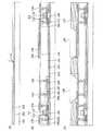
最初に、絶縁表面を有する基板101上に、下地層として機能する絶縁層102を形成する(図1(A)参照)。基板101には、ガラス基板、石英基板、シリコン基板、処理温度に耐えうる耐熱性を有するプラスチック基板を用いる。
First, the insulating
次に、絶縁層102に接するように、公知の方法(スパッタリング法、プラズマCVD法等)により、非晶質半導体層を形成する。次に、公知の結晶化法(レーザー結晶化法、熱結晶化法、ニッケルなどの触媒を用いた熱結晶化法等)により、非晶質半導体層を結晶化して、結晶質半導体層115を形成する。
Next, an amorphous semiconductor layer is formed by a known method (a sputtering method, a plasma CVD method, or the like) so as to be in contact with the insulating
次に、結晶質半導体層115をパターン加工して、島状の結晶質半導体層を形成した後、続いて、薄膜の成膜処理やエッチング処理、ドーピング処理等の所定の工程を経て、薄膜トランジスタ103、104と撮像素子105を形成する(図1(B)参照)。薄膜トランジスタ103、104と、撮像素子105とが含む半導体層は、共に、結晶質半導体層であり、また、共に、絶縁層102上に設けられている。このように、撮像素子105が含む半導体層を、薄膜トランジスタ103、104と同じ結晶質半導体層とすることにより、新たなマスクを追加することなく、基板101上に撮像素子105を作り込むことができる。
Next, after patterning the
但し、本発明は、上記の構成に制約されず、撮像素子105が含む半導体層として、光導電率が良好な非晶質半導体層や微結晶半導体層を用いてもよい。撮像素子105が含む半導体層として非晶質半導体層を形成し、薄膜トランジスタ103、104が含む半導体層として結晶質半導体層を形成する場合は、各素子で半導体層の結晶性が異なるために、作り分けが必要となる。従って、新たなマスクを追加する必要がある。
Note that the present invention is not limited to the above structure, and an amorphous semiconductor layer or a microcrystalline semiconductor layer with favorable photoconductivity may be used as a semiconductor layer included in the
なお、結晶性の異なる半導体層を作成するために、新たなマスクを追加する工程を用いず、レーザー光の照射を選択的に行う工程を用いてもよい。 Note that in order to create semiconductor layers having different crystallinity, a step of selectively irradiating laser light may be used without using a step of adding a new mask.
薄膜トランジスタ103は、不純物領域109とチャネル形成領域110とを含む結晶質半導体層と、ゲート絶縁層111と、ゲート電極114として機能する導電層112、113とを有する。薄膜トランジスタ103は、撮像素子105の動作を制御する。薄膜トランジスタ104は、不純物領域119とチャネル形成領域120とを含む結晶質半導体層と、ゲート絶縁層111と、ゲート電極121として機能する導電層122、123とを有する。薄膜トランジスタ104は、後に形成する発光素子142の動作を制御する。薄膜トランジスタ103、104のゲート電極は、導電性材料により単層又は積層で形成する。例えば、タングステン(W)/窒化タングステン(WN、タングステン(W)と窒素(N)の組成比は制約されない)の積層構造や、モリブデン(Mo)/アルミニウム(Al)/Mo、Mo/窒化モリブデン(MoN、モリブデン(Mo)と窒素(N)の組成比は制約されない)の積層構造を採用するとよい。
The
撮像素子105は、P型領域106と、I型領域107と、N型領域108とを有する。P型領域106と、I型領域107と、N型領域108とは、横に隣接して設けられている。P型領域106とI型領域107とN型領域108とを有する撮像素子105は、半導体の光効果によって起電力を生じる光起電力素子である。しかし、本発明において用いる撮像素子105は、光起電力素子だけでなく、光によって電気抵抗を変化させる光電導素子でもよい。光電導素子である場合、撮像素子105はP型領域とI型領域とP型領域、又はN型領域とI型領域とN型領域とを含む。
The
次に、薄膜トランジスタ103、104と、撮像素子105とを覆うように絶縁層124〜126を形成する。絶縁層124〜126は酸化珪素や窒化珪素等の無機材料、ポリイミドやアクリル等の有機材料等を用いて形成する。また、絶縁層124〜126は、シロキサン系の材料を用いてもよく、例えば、シリコンと酸素との結合で骨格構造が構成され、置換基に、少なくとも水素を含む有機基(例えばアルキル基、芳香族炭化水素)が用いられる。また、置換基として、フルオロ基を用いてもよい。また、置換基として、少なくとも水素を含む有機基とフルオロ基とを用いてもよい。
Next, insulating
次に、絶縁層124〜126に開口部を設けて、当該開口部を充填する導電層130〜135を形成する。導電層130〜135はソースドレイン配線(ソース配線、ドレイン配線)として機能する。導電層130〜135は、例えば、チタン(Ti)/アルミニウムシリコン(Al−Si、珪素(Si)が添加されたアルミニウム(Al))/Ti、Mo/Al−Si/Mo、MoN/Al−Si/MoNの積層構造を採用するとよい。または、アルミニウムを主成分としニッケルを含む材料、又は、アルミニウムを主成分とし、ニッケルと、炭素と珪素の一方又は両方とを含む合金材料を用いて形成するとよい。
Next, openings are provided in the insulating
次に、導電層134に接するように導電層136を形成する。導電層136は、発光素子の画素電極として機能する。導電層136には、透光性を有するインジウム錫酸化物(ITO)や、酸化珪素が添加されたITO、インジウム亜鉛酸化物(IZO)、ガリウム(Ga)をドープした酸化亜鉛(GZO)などを用いるとよい。
Next, the
次に、導電層130〜136を覆うように隔壁層137を形成する(図1(C)参照)。隔壁層137には2つの開口部138、139が設けられており、1つの開口部138は、撮像素子105と重なる位置に設けられている。もう一つの開口部139は、導電層136が露出するように設けられている。また、隔壁層137は、遮光性を有するものであり、カーボン粒子、金属粒子、顔料や着色料等を添加して撹拌した後、必要に応じて濾過を行い、その後、スピンコート法で形成する。なお、有機材料にカーボン粒子や金属粒子を添加する際は、均一に混合されるように、界面活性剤や分散剤などを添加してもよい。
Next, a
隔壁層(遮光性を有する層ともよぶ)137は、まず、絶縁層126と導電層130〜136を覆うように絶縁層を形成し、次に、当該絶縁層の所望の箇所を選択的に除去したものである。つまり、開口部138、139とは、隔壁層137において、選択的に除去された部分に相当する。隔壁層137は、段差部を有する。
For the partition layer (also referred to as a light-blocking layer) 137, an insulating layer is formed so as to cover the insulating
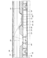
次に、導電層136に接するように電界発光層140を形成する(図2参照)。続いて、電界発光層140に接するように導電層141を形成する。導電層141は対向電極として機能する。導電層136と、電界発光層140と、導電層141の積層体が発光素子142に相当する。次に、基板101と対向する対向基板143を設ける。なお、図示しないが、基板101の一表面と、対向基板143の一表面に、円偏光板などの光学フィルムを設けてもよい。
Next, the
上記のような工程を経て完成する本発明の読み取り機能付き表示装置は、表示機能と読み取り機能を有する。表示機能を用いるときは、対向基板143の方向に、発光素子142を点灯(発光)又は非点灯(非発光)させて、画像を表示する。一方、読み取り機能を用いるときは、対向基板143の方向に発光素子142を点灯させ、読み取り対象物144において反射した光が撮像素子105に入ることにより、読み取り対象物144の情報を読み取る。
The display device with a reading function of the present invention completed through the above steps has a display function and a reading function. When using the display function, the
本発明の読み取り機能付き表示装置は、主に、絶縁表面を有する基板101上に設けられた薄膜トランジスタ103、104及び撮像素子105と、薄膜トランジスタ103、104及び撮像素子105を覆う絶縁層124〜126と、絶縁層124〜126上に設けられた発光素子142と、発光素子142の端部を囲み、遮光性を有する隔壁層137とを有する。そして、隔壁層137は、撮像素子105と重なる位置に、開口部138を有することを特徴とする。
The display device with a reading function of the present invention mainly includes
本発明は、発光素子の端部を囲む隔壁層137として、遮光性を有する材料を用いることにより、読み取り対象物144に反射していない光が撮像素子105に入ることを防止する。また、隔壁層137は、撮像素子105と重なる位置に、開口部を有するため、読み取り対象物144に反射した光が、遮光性を有する隔壁層137に吸収されることなく、撮像素子105に入り、読み取り対象物144の情報を読み取ることができる。
In the present invention, a light-blocking material is used as the
このように、隔壁層137が遮光性を有すると、画素間の輪郭(画素間の境界)が明瞭なものとなるため、高精細な画像を表示することができる。また、外部から入る光の反射が低減され、映り込みを防止することができるため、偏光板などの光学フィルムが不要となり、小型化、薄型化、軽量化を実現する。
As described above, when the
なお、発光素子142から発せられる光の方向は特に制約されないが、上述の通り、隔壁層137を遮光性にして、不要光を削減又は除去するという点から、発光素子142から発せられる光が対向基板143の方に向かう上面出射か、又は、発光素子142から発せられる光が基板101と対向基板143の両者に向かう両面出射の場合が有効である。また、上面出射と両面出射と比較して、効果は少なくなるものの、発光素子142から発せられる光が基板101の方向に向かう下面出射でもよい。
Note that the direction of light emitted from the light-emitting
上面出射を行う場合であって、発光素子142の動作を制御する薄膜トランジスタ104の導電型がN(Nチャネル型)型の場合、発光素子142の画素電極が陰極、対向電極が陽極の逆積み構造となるようにする。また、薄膜トランジスタの導電型がP型(Pチャネル型)の場合、発光素子142の画素電極が陽極、対向電極が陰極の順積み構造となるようにする。この際、画素電極の下部に反射体を設けて、発光素子142から発せられる光が対向基板143側に向かうようにする。図2に示す断面構造は、上記の構成を採用したものであり、発光素子142の画素電極として機能する導電層136の下部に、反射体となる導電層134を設けている。
When top emission is performed and the
両面出射を行う場合、発光素子142の画素電極と対向電極の両者を、透光性を有する材料か、又は、光を透過する厚さで形成する。
In the case of performing dual emission, both the pixel electrode and the counter electrode of the light-emitting
下面出射を行う場合であって、薄膜トランジスタ104の導電型がN型の場合、発光素子142の画素電極が陰極、対向電極が陽極の逆積み構造となるようにする。この際、対向電極の上部に反射体を設けて、発光素子142から発せられる光が基板101側に向かうようにする。また、薄膜トランジスタ104の導電型がP型の場合、発光素子142の画素電極が陽極、対向電極が陰極の順積み構造となるようにする。
When bottom emission is performed and the conductivity type of the
また、本発明の読み取り機能付き表示装置は、赤・緑・青のいずれかの色を発光する発光素子を用いる形態に制約されず、白色発光素子と着色層、又は青色発光素子と色変換層を用いてもよい。そこで、白色発光素子と着色層を用いたときの読み取り機能付き表示装置の断面構造について図面を参照して説明する。 Further, the display device with a reading function of the present invention is not limited to a form using a light emitting element that emits one of red, green, and blue, and a white light emitting element and a colored layer, or a blue light emitting element and a color conversion layer. May be used. Therefore, a cross-sectional structure of a display device with a reading function when a white light emitting element and a colored layer are used will be described with reference to the drawings.
基板101上に、撮像素子151〜153と薄膜トランジスタ154〜156が設けられ、撮像素子151〜153と薄膜トランジスタ154〜156を覆うように絶縁層124〜126が設けられる(図3参照)。絶縁層124〜126上に白色発光素子157〜159が設けられ、白色発光素子157〜159の端部を囲む隔壁層137が設けられる。隔壁層137は、撮像素子151〜153と重なる位置に、開口部164〜166を有する。
そして、基板101と対向するように、着色層161〜163を含む対向基板143が設けられる。着色層161〜163のうち、1つは赤色に対応し、1つは緑色に対応し、1つは青色に対応する。白色発光素子157〜159は、着色層161〜163のいずれかを介すると、赤・緑・青のいずれかの色の光を発する。
A
青色発光素子と色変換層を用いる場合には、白色発光素子157〜159を青色発光素子とし、着色層161〜163を色変換層とすればよい。
In the case of using a blue light emitting element and a color conversion layer, the white
上記構成では、白色発光素子157〜159の各々が発光する光は、着色層161〜163の各々を通過し、読み取り対象物144の表面に達する。そして、読み取り対象物144の表面において反射した光を、撮像素子151〜153の各々が受光することにより、読み取り対象物144の情報を読み取ることができる。
In the above configuration, the light emitted from each of the white
上記構成のように、発光素子の光の出射側に、ある波長帯の光を透過する着色層又は色変換層を設けた構成とすると、色純度の向上や、画素部の鏡面化(映り込み)の防止を図ることができる。また、着色層又は色変換層を設けると、従来必要であるとされていた円偏光板等を省略することが可能となり、電界発光層から出射する光の損失を無くすことができる。さらに、斜方から画素領域を見た場合に起こる色調の変化を低減することができる。また、白色発光素子又は青色発光素子を用いる場合は、電界発光層を塗り分ける必要がないため、その工程を短縮させて低コスト化を実現する。 When a colored layer or a color conversion layer that transmits light in a certain wavelength band is provided on the light emitting side of the light emitting element as in the above configuration, the color purity is improved and the pixel portion is mirrored (reflected). ) Can be prevented. In addition, when a colored layer or a color conversion layer is provided, it is possible to omit a circularly polarizing plate that has been conventionally required, and it is possible to eliminate a loss of light emitted from the electroluminescent layer. Furthermore, a change in color tone that occurs when the pixel region is viewed obliquely can be reduced. In addition, when a white light emitting element or a blue light emitting element is used, it is not necessary to coat the electroluminescent layer separately, so that the process can be shortened to realize cost reduction.
続いて、図1〜図3に示した断面構造を有する本発明の読み取り機能付き表示装置の構成について図面を参照して説明する。 Next, the configuration of the display device with a reading function of the present invention having the cross-sectional structure shown in FIGS. 1 to 3 will be described with reference to the drawings.
本発明の読み取り機能付き表示装置は、絶縁表面を有する基板101上に、ソースドライバ202、ゲートドライバ203、センサ用ソースドライバ204、センサ用ゲートドライバ205、複数の画素206がマトリクス状に設けられた画素領域207とを有する(図4(A)参照)。画素206は、複数の副画素を有し、少なくとも、発光素子を含む副画素を1つと、撮像素子を含む副画素を1つとを有する。ソースドライバ202とゲートドライバ203は発光素子を含む副画素の動作を制御し、センサ用ソースドライバ204とセンサ用ゲートドライバ205は撮像素子を含む副画素の動作を制御する。
In the display device with a reading function of the present invention, a
画素206には、様々な構成が適用されるが、例えば、赤色に発光する第1の発光素子を含む第1の副画素211と、緑色に発光する第2の発光素子を含む第2の副画素212と、青色に発光する第3の発光素子を含む第3の副画素213と、撮像素子を含む第4の副画素214とを有する場合がある(図4(B)参照)。第1の副画素211〜第4の副画素214の各々は、発光素子又は撮像素子を制御する薄膜トランジスタを含む。
Although various configurations are applied to the
上記構成を有する場合、点灯する副画素を切り換えて、その度に画像を読み取る。その後、読み取った情報を合成することで、読み取り対象物のカラーの情報を得ることができる。具体的には、例えば、第1の副画素211を点灯させて、第4の副画素214により読み取り対象物の情報を読み取り、次に、第2の副画素212を点灯させて、第4の副画素214により読み取り対象物の情報を読み取り、最後に、第3の副画素213を点灯させて、第4の副画素214により読み取り対象物の情報を読み取る。その後、読み取った3つの情報を合成すれば、読み取り対象物のカラーの情報を得ることができる。この構成の場合、3回の読み取りで、読み取り対象物のカラーの情報を得ることができる。
In the case of the above configuration, the subpixel to be turned on is switched, and the image is read each time. Thereafter, by combining the read information, the color information of the reading object can be obtained. Specifically, for example, the
また、画素206の別の構成として、赤色に発光する第1の発光素子を含む第1の副画素211と、緑色に発光する第2の発光素子を含む第2の副画素212と、青色に発光する第3の発光素子を含む第3の副画素213と、第1の撮像素子を含む第4の副画素214と、第2の撮像素子を含む第5の副画素215と、第3の撮像素子を含む第6の副画素216とを有する場合がある(図4(C)参照)。第1の副画素211〜第6の副画素216の各々は、発光素子又は撮像素子を制御する薄膜トランジスタを含む。
As another configuration of the
また、第1の副画素211及び第4の副画素214と、第2の副画素212及び第5の副画素215と、第3の副画素213及び第6の副画素216の各々は、隣接して設けられる。また、第1の副画素211と第4の副画素214とを足した面積と、第2の副画素212と第5の副画素215とを足した面積と、第3の副画素213と第6の副画素216とを足した面積は、同じ又はほぼ同じである。
In addition, the
上記構成を有する場合、第1の副画素211〜第3の副画素213を同時に点灯させて、第4の副画素214〜第6の副画素216の副画素により読み取り対象物の情報を読み取る。第4の副画素214は第1の副画素211が発した光の反射光を受け取り、第5の副画素215は第2の副画素212が発した光の反射光を受け取り、第6の副画素216は第3の副画素213が発した光の反射光を受け取る。この構成の場合、1回の読み取りで、読み取り対象物のカラーの情報を得ることができる。なお、ここで述べる反射光とは、発光素子から発せられた光が読み取り対象物の表面において反射した光である。
In the case of the above configuration, the
また、画素206の別の構成として、発光素子を含む第1の副画素211〜第3の副画素213と、撮像素子を含む副画素226、227とを有する場合がある(図5(A)参照)。副画素226、227は、第1の副画素211〜第3の副画素213の反射光を受け取る。この構成では、3回の読み取りで、読み取り対象物のカラーの情報を得ることができる。
As another structure of the
また、画素206の別の構成として、発光素子を含む第1の副画素211〜第3の副画素213と、撮像素子を含む副画素220〜225とを有する場合がある(図5(B)参照)。副画素220、223は、第1の副画素211の反射光を受け取り、副画素221、224は第2の副画素212の反射光を受け取り、副画素222、225は第3の副画素213の反射光を受け取る。この構成では、1回の読み取りで、読み取り対象物のカラーの情報を得ることができる。
As another structure of the
また、画素206の別の構成として、発光素子を含む第1の副画素211〜第3の副画素213と、撮像素子を含む副画素230〜241とを有する場合がある(図5(C)参照)。副画素230、231、236、237は第1の副画素211の反射光を受け取り、副画素232、233、238、239は第2の副画素212の反射光を受け取り、副画素234、235、240、241は第3の副画素213の反射光を受け取る。この構成でも、1回の読み取りで、読み取り対象物のカラーの情報を得ることができる。
As another structure of the
また、上記記載の画素206の形状は矩形状であったが、本発明はこの形状に制約されず、例えば、六角形状などの多角形状でもよいし(図5(D)参照)、円状でもよい。
Further, although the shape of the
なお上記の記載では、第1の副画素211〜第3の副画素213が赤・緑・青のいずれかの色を発光する発光素子を有する場合を説明したが、本発明は、この場合に制約されない。例えば、第1の副画素211は、外部に出される光が赤色であればよいため、白色に発光する発光素子と赤色の着色層、又は、青色に発光する発光素子と色変換層を有していればよい。また、第2の副画素212は、外部に出される光が緑色であればよいため、白色発光素子と緑色の着色層、又は青色発光素子と色変換層を有していればよい。また、第3の副画素213は、外部に出される光が青色であればよいため、白色発光素子と青色の着色層、又は青色発光素子と色変換層を有していればよい。
(実施の形態2)
In the above description, the case where the
(Embodiment 2)
本発明の読み取り機能付き表示装置が含む画素206は、複数の副画素を有し、少なくとも発光素子を含む副画素を1つと、撮像素子を含む副画素を1つ有することは上述した通りである。そして、以下には、基板上に設けられる副画素の面積を変えることを特徴とした読み取り機能付き表示装置の構成について説明する。
As described above, the
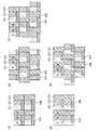
まず、第1の構成について、図面を参照して説明する。画素206は、赤色に発光する発光素子を含む第1の副画素211と、緑色に発光する発光素子を含む第2の副画素212と、青色に発光する発光素子を含む第3の副画素213と、撮像素子を含む第4の副画素214とを有する(図6(A)〜(E)参照)。基板上における、第1の副画素211の面積と第3の副画素213の面積は同じ又は概略同じであり、第2の副画素212の面積と第4の副画素214の面積を足した面積は、第1の副画素211の面積、又は第3の副画素213の面積と同じ又は概略同じである。
First, the first configuration will be described with reference to the drawings. The
なお、第2の副画素212の面積と第4の副画素214の面積との面積比は、例えば、第2の副画素212の面積:第4の副画素214の面積=3:1にするようにしてもよいし(図6(A)〜(C)参照)、第2の副画素212の面積:第4の副画素214の面積=5:1にするようにしてもよい(図6(D)(E)参照)。この面積比は、赤・緑・青の発光材料の電流密度に応じて定めればよく、各色の輝度のバラツキが改善されるような面積比にするとよい。また、第2の副画素212の面積と第4の副画素214の面積を横に分割してもよいし(図6(A)〜(C)参照)、縦に分割してもよい。また、画素206が含む第1の副画素211〜第4の副画素214の配列は、赤・緑・青に対応した副画素をストライプ状に配列したストライプ配列(図6(A)(D)参照)、1ライン毎に半ピッチずらしたデルタ配列(図6(B)(E)参照)、赤・緑・青に対応した副画素を斜めに配列するモザイク配列(図6(C)参照)のいずれの配列方法を採用してもよい。ストライプ配列は、線、図形、文字の表示などに適しているため、モニターに適用することが好ましい。また、モザイク配列は、ストライプ配列よりも自然な画像が得られるため、テレビジョン装置等に適用することが好ましい。また、デルタ配列も自然な画像表示が得られるため、テレビジョン装置等に適用することが好ましい。
The area ratio between the area of the
次に、第2の構成について、図面を参照して説明する。画素206は、赤色に発光する発光素子を含む第1の副画素211と、緑色に発光する発光素子を含む第2の副画素212と、青色に発光する発光素子を含む第3の副画素213と、撮像素子を含む第4の副画素214とを有する(図7(A)〜(E)参照)。そして、基板101上における、第1の副画素211の面積と第2の副画素212の面積と第4の副画素214の面積とを足した面積は、第3の副画素213の面積の2倍又は概略2倍である。
Next, the second configuration will be described with reference to the drawings. The
なお、第1の副画素211の面積と、第2の副画素212の面積と、第4の副画素214の面積の面積比は、例えば、第1の副画素211の面積:第2の副画素212の面積:第4の副画素214の面積=1:1:1にしてもよいし(図7(A)〜(C)参照)、第1の副画素211の面積:第2の副画素212の面積:第4の副画素214の面積=5:4:3にしてもよい(図7(D)(E)参照)。この面積比は、赤・緑・青の発光材料の電流密度に応じて定めればよく、各色の輝度のバラツキが改善されるような面積比にするとよい。また、第1の副画素211〜第4の副画素214の配列は、ストライプ配列(図7(A)(D)参照)、デルタ配列(図7(B)(E)参照)、モザイク配列(図7(C)参照)のいずれの配列方法を採用してもよい。
The area ratio of the area of the
なお、上述した通り、第1の副画素211、第2の副画素212、第3の副画素213及び第4の副画素214の面積比は、赤、緑、青の発光材料の電流密度に応じて定めればよい。例えば、第1の副画素211、第2の副画素212及び第3の副画素213から選択された1つの副画素の面積と第4の副画素214の面積を足した面積は、第1の副画素211、第2の副画素212及び第3の副画素213から選択された残りの2つの副画素の面積の0.5倍にすればよい。また、第1の副画素211、第2の副画素212及び第3の副画素213から選択された2つの副画素の面積と第4の副画素214の面積を足した面積は、第1の副画素211、第2の副画素212及び第3の副画素213から選択された残りの1つの副画素の面積の2倍にすればよい。
Note that as described above, the area ratio of the
本発明の読み取り機能付き表示装置が含む画素206は、複数の副画素を有し、少なくとも発光素子を含む副画素を1つと、撮像素子を含む副画素を1つ有する。ここでは、画素206の等価回路の一例について、図面を参照して説明する。
The
まず、画素206が、赤色に発光する第1の発光素子を含む第1の副画素211と、緑色に発光する第2の発光素子を含む第2の副画素212と、青色に発光する第3の発光素子を含む第3の副画素213と、撮像素子を含む第4の副画素214とを有する場合の等価回路図について説明する(図8参照)。
First, the
第1の副画素211〜第3の副画素213の各々は、ソース線Sx(xは自然数)と、電源線Vxと、ゲート線Gy(yは自然数)とに囲まれた領域に、スイッチ用トランジスタ250と、駆動用トランジスタ251と、容量素子252と、発光素子253とを有する。スイッチ用トランジスタ250は、副画素に対するビデオ信号の入力を制御するトランジスタであり、その導電型はN型、P型のどちらでもよい。駆動用トランジスタ251は、発光素子253に流れる電流値を制御するトランジスタであり、その導電型はN型、P型のどちらでもよい。容量素子252は、副画素に入力されたビデオ信号を保持する役割を担う。なお、図示する構成では、スイッチ用トランジスタ250の導電型をN型とし、駆動用トランジスタ251の導電型をP型としている。
Each of the
第4の副画素214は、ソース線Sam(mは自然数)と、リセット線Rn(nは自然数)と、電源線Vamと、ゲート線Ganとに囲まれた領域に、選択用トランジスタ254と、増幅用トランジスタ255と、リセット用トランジスタ256と、撮像素子257とを有する。リセット用トランジスタ256は、撮像素子257の一端の領域と他端の領域の電位差をリセットするトランジスタである。増幅用トランジスタ255は、撮像素子257から読み取った信号を増幅するトランジスタである。選択用トランジスタ254は、センサ用ソースドライバに対する撮像素子257が読み取った信号の供給を制御する。なお、図示する構成では、選択用トランジスタ254と増幅用トランジスタ255の導電型をP型とし、リセット用トランジスタ256の導電型をN型としている。
The
次に、赤色に発光する第1の発光素子を含む第1の副画素211と、緑色に発光する第2の発光素子を含む第2の副画素212と、青色に発光する第3の発光素子を含む第3の副画素213と、第1の撮像素子を含む第4の副画素214と、第2の撮像素子を含む第5の副画素215と、第3の撮像素子を含む第6の副画素216とを有する場合の等価回路図について説明する(図9参照)。
Next, a
この場合も、上記の画素の構成と同様に、第1の副画素211〜第3の副画素213は、スイッチ用トランジスタ250と、駆動用トランジスタ251と、容量素子252と、発光素子253とを有し、第4の副画素214〜第6の副画素216は選択用トランジスタ254と、増幅用トランジスタ255と、リセット用トランジスタ256と、撮像素子257とを有する。本実施例は、上記の実施の形態と自由に組み合わせることができる。
Also in this case, similarly to the pixel configuration described above, the
本実施例は、本発明の読み取り機能付き表示装置の一形態であるパネルの構成について図面を参照して説明する。パネルは、絶縁表面を有する基板101上に、ソースドライバ202、ゲートドライバ203、センサ用ソースドライバ204、センサ用ゲートドライバ205、複数の画素がマトリクス状に設けられた画素領域207、接続フィルム401、基板101と対向する対向基板143とを有する(図10(A)参照)。接続フィルム401は外部のICチップに接続する。
In this embodiment, a structure of a panel which is an embodiment of the display device with a reading function of the present invention will be described with reference to the drawings. The panel includes a
図10(B)はパネルのA−Bにおける断面図を示し、画素領域207に設けられた撮像素子405、発光素子406及び駆動用トランジスタ407と、ソースドライバ202に設けられたCMOS素子404を示す。なお、図10(B)では、センサ用ソースドライバ204に設けられた素子の断面構造の記載は省略する。
FIG. 10B is a cross-sectional view taken along the line AB of the panel, and shows an
画素領域207と上記の4つのドライバの周囲には、シール材403が設けられ、基板101と対向基板143がシール材403により貼り合わされている。このような処理は、発光素子406を水分から保護するための処理であり、ここではカバー材(ガラス、セラミックス、プラスチック、金属等)により封止する方法を用いるが、熱硬化性樹脂や紫外光硬化性樹脂を用いて封止する方法、金属酸化物や窒化物等のバリア能力が高い薄膜により封止する方法を用いてもよい。
A sealing
また、ここでは、基板101上に形成される素子は、非晶質半導体に比べて移動度等の特性が良好な結晶質半導体(ポリシリコン)により形成しているため、モノリシック化が実現される。従って、接続する外部ICの個数が減少させて、小型・軽量・薄型を実現することができる。
Here, since the element formed over the
また、本発明の読み取り機能付き表示装置に、タッチパネル機能を設けることもできる。これは、入力ペン402のペン先において光を反射させることにより行う。つまり、この機能では、発光素子406から発せられた光が入力ペン402のペン先において反射し、その反射した光が撮像素子405に入ることにより、入力ペン402が指し示した位置が認識される。
The display device with a reading function of the present invention can be provided with a touch panel function. This is done by reflecting light at the pen tip of the
従来のタッチパネル機能を設けた装置として、抵抗膜を用いたものがあるが、この方式は、表示画面の表面に抵抗膜が必要であった。そうすると、使用者は、抵抗膜を介して画像を見ることになるため、画像の輝度を損なうことがあった。また、使用するほど、変形して破壊することがあり、耐久性に問題があった。また、破壊までには至らないとしても、変形により、ペン入力の検出精度に問題が発生することがあった。しかしながら、本発明の読み取り機能付き表示装置にタッチパネル機能を設けた場合、表示する画像の輝度を損なうことなく、鮮明な画像を表示することができる。また、耐久性に優れ、検出精度が良好な状態を維持することができる。本実施例は、上記の実施の形態、実施例と自由に組み合わせることができる。 As a conventional device provided with a touch panel function, there is a device using a resistance film, but this method requires a resistance film on the surface of the display screen. Then, since the user views the image through the resistance film, the brightness of the image may be impaired. In addition, as it is used, it may be deformed and destroyed, and there is a problem in durability. Moreover, even if it does not lead to destruction, a problem may occur in detection accuracy of pen input due to deformation. However, when the display device with a reading function of the present invention is provided with a touch panel function, a clear image can be displayed without impairing the luminance of the displayed image. Moreover, it is excellent in durability and can maintain a state with good detection accuracy. This embodiment can be freely combined with the above embodiment modes and embodiments.
本実施例では、本発明の読み取り機能付き表示装置を含む電子機器について図面を参照して説明する。発光素子を含む画素領域を備えた電子機器として、テレビジョン装置(単にテレビ、テレビジョン受信機ともよぶ)、デジタルカメラ、デジタルビデオカメラ、携帯電話装置(単に携帯電話機、携帯電話ともよぶ)やPDA等の携帯情報端末、携帯型ゲーム機、コンピュータ用のモニター、カーオーディオ等の音響再生装置、家庭用ゲーム機等が挙げられる。その具体例について、図11を参照して説明する。 In this embodiment, an electronic device including a display device with a reading function according to the present invention will be described with reference to the drawings. As electronic devices having a pixel region including a light-emitting element, a television device (also simply referred to as a television or a television receiver), a digital camera, a digital video camera, a mobile phone device (also simply referred to as a mobile phone or a mobile phone), or a PDA Mobile information terminals such as personal computer, portable game machines, computer monitors, sound reproduction devices such as car audio, and home game machines. A specific example will be described with reference to FIG.
携帯電話機は、読み取り機能付き表示部9102等を含んでいる(図11(A)参照)。読み取り機能付き表示部9102には、実施の形態1、2で示すものを適用することができる。
The cellular phone includes a
携帯情報端末は、読み取り機能付き表示部9301、入力ペン9302等を含んでいる(図11(B)参照)。読み取り機能付き表示部9301は、実施の形態1、2で示すものを適用することができる。
The portable information terminal includes a
デジタルビデオカメラは、読み取り機能付き表示部9701、9702等を含んでいる(図11(C)参照)。読み取り機能付き表示部9701、9702は、実施の形態1、2で示すものを適用することができる。
The digital video camera includes
携帯型ゲーム機は、読み取り機能付き表示部9402等を含んでいる(図11(D)参照)。読み取り機能付き表示部9402は、実施の形態1、2で示すものを適用することができる。
The portable game machine includes a
携帯情報端末は、読み取り機能付き表示部9202等を含んでいる(図11(E)参照)。読み取り機能付き表示部9202は、実施の形態1、2で示すものを適用することができる。
The portable information terminal includes a
モニター装置は、読み取り機能付き表示部9502、入力ペン9503等を含んでいる(図11(F)参照)。読み取り機能付き表示部9502は、実施の形態1、2で示すものを適用することができる。
The monitor device includes a
本発明の読み取り機能付き表示装置を適用することで、表示機能だけではなく、読み取り機能を設けることができるため、高機能化と高付加価値化を実現した電子機器を提供することができる。また、入力ペンも設けることで、タッチパネル機能も追加することができ、さらなる高機能化と高付加価値化を実現した電子機器を提供することができる。 By applying the display device with a reading function of the present invention, not only a display function but also a reading function can be provided, so that an electronic device with high functionality and high added value can be provided. In addition, by providing an input pen, a touch panel function can be added, and an electronic device that realizes further higher functionality and higher added value can be provided.
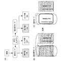
本発明の読み取り機能付き表示装置は、表示機能と読み取り機能の2つの機能を有する。本実施例は、両機能の切り換えシステムについて、図面を参照して説明する。 The display device with a reading function of the present invention has two functions of a display function and a reading function. In this embodiment, a switching system for both functions will be described with reference to the drawings.
まず、本発明の読み取り機能付き表示装置の電源を入れて起動する(図12(A)参照)。起動後は、まず自動的に表示モードになり、表示部がオン、センサ部はオフとなる。ここで述べる表示部とは、発光素子を含む副画素と、その副画素を制御するドライバに相当する。また、センサ部とは、撮像素子を含む副画素と、その副画素を制御するドライバに相当する。 First, the display device with a reading function of the present invention is turned on and started (see FIG. 12A). After startup, the display mode is automatically entered first, the display unit is turned on, and the sensor unit is turned off. The display portion described here corresponds to a subpixel including a light emitting element and a driver that controls the subpixel. The sensor unit corresponds to a subpixel including an image sensor and a driver that controls the subpixel.
続いて、表示モードから読み取りモードに移るときは、表示装置に設けられたボタンや入力ペン等を用いて行う。読み取りモードでは、表示部とセンサ部の両者がオンとなる。また、読み取りモードから表示モードに移るときも、表示装置に設けられたボタンや入力ペン等を用いて行う。 Subsequently, when the display mode is changed to the reading mode, the buttons and the input pen provided on the display device are used. In the reading mode, both the display unit and the sensor unit are turned on. Further, when the mode is changed from the reading mode to the display mode, it is performed by using a button or an input pen provided on the display device.
本発明の読み取り機能付き表示装置は、PDAや携帯電話等の携帯端末に最適であり、例えば、読み取りモードにした後、表示画面上に名刺をおけば、素早く画像を読み取り(図12(B)参照)、その後、読み取りモードから表示モードに変えた後、同じ表示画面上に、読み取った画像を表示することができる(図12(C)参照)。 The display device with a reading function of the present invention is most suitable for a portable terminal such as a PDA or a mobile phone. For example, if a business card is placed on the display screen after entering the reading mode, the image is quickly read (FIG. 12B). After that, after changing from the reading mode to the display mode, the read image can be displayed on the same display screen (see FIG. 12C).
また、読み取り対象物として、名刺だけではなく、指紋等の人体の生体情報を読み取ることもできる。生体情報が読み取れれば、認証機能を行うことができる。例えば、まず、携帯端末の画面に指を密着させて、指紋の情報を読み取る(図13(A)の上面図と図13(B)の断面図参照)。指紋の情報とは、具体的には、指紋の端点と分岐点の情報である(図13(C)参照)。指紋の端点と分岐点の情報の読み取りが終了したら、その情報と、前もって記憶されていたデータベース内の指紋情報とを照合する(図13(D)参照)。又は、ID番号の入力も同時に行うことにより、データベース内の指紋情報を特定し、その特定した指紋情報と照合する。このような個人認証機能を用いれば、他人が自分の携帯端末を使用することを防止したり、携帯端末を用いて電子商取引を行ったりすることができる。 Further, not only business cards but also human body biometric information such as fingerprints can be read as an object to be read. If biometric information can be read, an authentication function can be performed. For example, first, a finger is brought into close contact with the screen of the portable terminal to read fingerprint information (see a top view in FIG. 13A and a cross-sectional view in FIG. 13B). Specifically, the fingerprint information is information on the end points and branch points of the fingerprint (see FIG. 13C). When reading of the fingerprint end point and branch point information is completed, the information is compared with the fingerprint information stored in the database in advance (see FIG. 13D). Alternatively, the fingerprint information in the database is specified by inputting the ID number at the same time, and collated with the specified fingerprint information. By using such a personal authentication function, it is possible to prevent others from using their mobile terminals or to conduct electronic commerce using the mobile terminals.
101 基板
102 絶縁層
103 薄膜トランジスタ
104 薄膜トランジスタ
105 撮像素子
106 P型領域
107 I型領域
108 N型領域
109 不純物領域
110 チャネル形成領域
111 ゲート絶縁層
112 導電層
113 導電層
114 ゲート電極
115 結晶質半導体層
119 不純物領域
120 チャネル形成領域
121 ゲート電極
122、123 導電層
124〜126 絶縁層
130〜136 導電層
137 隔壁層
138、139 開口部
140 電界発光層
141 導電層
142 発光素子
143 対向基板
144 読み取り対象物
151〜153 撮像素子
154〜156 薄膜トランジスタ
157〜159 白色発光素子
161〜163 着色層
164〜166 開口部
DESCRIPTION OF
Claims (7)
前記複数の画素の各々は、
薄膜トランジスタと、
撮像素子と、
前記薄膜トランジスタ及び前記撮像素子上に設けられた絶縁層と、
前記絶縁層上に設けられた第1の導電層と、
前記絶縁層上に設けられた遮光性を有する層と、
前記第1の導電層及び前記遮光性を有する層上に設けられた発光層と、
前記発光層上に設けられた第2の導電層と、を有し、
前記薄膜トランジスタは、前記撮像素子と電気的に接続されており、
前記遮光性を有する層は、前記第1の導電層の端部及び前記薄膜トランジスタを覆って設けられており、
前記遮光性を有する層は、前記撮像素子と重なる位置に設けられた開口部を有することを特徴とする読み取り機能付き表示装置。 Having a plurality of pixels on a substrate having an insulating surface;
Each of the plurality of pixels is
A thin film transistor;
An image sensor;
An insulating layer provided on the thin film transistor and the imaging device;
A first conductive layer provided on the insulating layer;
A light-shielding layer provided on the insulating layer;
A light emitting layer provided on the first conductive layer and the light-shielding layer;
A second conductive layer provided on the light emitting layer,
The thin film transistor is electrically connected to the image sensor,
The light-shielding layer is provided so as to cover an end portion of the first conductive layer and the thin film transistor,
The display device with a reading function, wherein the light-shielding layer has an opening provided at a position overlapping with the imaging element.
前記複数の画素の各々は、
第1の薄膜トランジスタと、
第2の薄膜トランジスタと、
撮像素子と、
前記第1の薄膜トランジスタ、前記第2の薄膜トランジスタ、及び前記撮像素子上に設けられた絶縁層と、
前記絶縁層上に設けられた第1の導電層と、
前記絶縁層上に設けられた遮光性を有する層と、
前記第1の導電層及び前記遮光性を有する層上に設けられた発光層と、
前記発光層上に設けられた第2の導電層と、を有し、
前記遮光性を有する層は、前記第1の導電層の端部、前記第1の薄膜トランジスタ、及び前記第2の薄膜トラジスタを覆って設けられており、
前記遮光性を有する層は、前記撮像素子と重なる位置に設けられた開口部を有し、
前記第1の薄膜トランジスタは、前記第1の導電層、前記発光層、及び前記第2の導電層を有する発光素子の動作を制御する機能を有し、
前記第2の薄膜トランジスタは、前記撮像素子を制御する機能を有することを特徴とする読み取り機能付き表示装置。 Having a plurality of pixels on a substrate having an insulating surface;
Each of the plurality of pixels is
A first thin film transistor;
A second thin film transistor;
An image sensor;
An insulating layer provided on the first thin film transistor, the second thin film transistor, and the imaging element;
A first conductive layer provided on the insulating layer;
A light-shielding layer provided on the insulating layer;
A light emitting layer provided on the first conductive layer and the light-shielding layer;
A second conductive layer provided on the light emitting layer,
The light-shielding layer is provided so as to cover an end portion of the first conductive layer, the first thin film transistor, and the second thin film transistor,
The light-shielding layer has an opening provided at a position overlapping the image sensor,
The first thin film transistor has a function of controlling an operation of a light emitting element having the first conductive layer, the light emitting layer, and the second conductive layer,
The display device with a reading function, wherein the second thin film transistor has a function of controlling the imaging element.
前記発光素子及び前記遮光性を有する層上に、着色層を有することを特徴とする読み取り機能付き表示装置。 In claim 2,
A display device with a reading function, comprising a colored layer on the light-emitting element and the light-shielding layer.
前記第1の薄膜トランジスタと電気的に接続された、ソース配線またはドレイン配線として機能する導電層を有し、
前記ソース配線またはドレイン配線として機能する導電層は、反射体としての機能を有することを特徴とする読み取り機能付き表示装置。 In claim 2 or claim 3 ,
A conductive layer electrically connected to the first thin film transistor and functioning as a source wiring or a drain wiring;
The display device with a reading function, wherein the conductive layer functioning as the source wiring or the drain wiring has a function as a reflector.
前記撮像素子が有する半導体層、前記第1の薄膜トランジスタが有する第1の半導体層、及び前記第2の薄膜トランジスタが有する第2の半導体層は、同一材料を用いて設けられていることを特徴とする読み取り機能付き表示装置。 In any one of Claims 2 thru | or 4,
The semiconductor layer in which the image pickup element has a first semiconductor layer having said first thin film transistor, and a second semiconductor layer having said second thin film transistor is characterized in that is provided with the same material Display device with reading function.
前記基板はプラスチック基板であることを特徴とする読み取り機能付き表示装置。 In any one of Claims 1 thru | or 5 ,
The display device with a reading function, wherein the substrate is a plastic substrate.
Priority Applications (1)
| Application Number | Priority Date | Filing Date | Title |
|---|---|---|---|
| JP2005206342A JP5364227B2 (en) | 2004-07-16 | 2005-07-15 | Display device with reading function and electronic device using the same |
Applications Claiming Priority (3)
| Application Number | Priority Date | Filing Date | Title |
|---|---|---|---|
| JP2004210103 | 2004-07-16 | ||
| JP2004210103 | 2004-07-16 | ||
| JP2005206342A JP5364227B2 (en) | 2004-07-16 | 2005-07-15 | Display device with reading function and electronic device using the same |
Publications (3)
| Publication Number | Publication Date |
|---|---|
| JP2006065305A JP2006065305A (en) | 2006-03-09 |
| JP2006065305A5 JP2006065305A5 (en) | 2008-08-14 |
| JP5364227B2 true JP5364227B2 (en) | 2013-12-11 |
Family
ID=36111803
Family Applications (1)
| Application Number | Title | Priority Date | Filing Date |
|---|---|---|---|
| JP2005206342A Expired - Fee Related JP5364227B2 (en) | 2004-07-16 | 2005-07-15 | Display device with reading function and electronic device using the same |
Country Status (1)
| Country | Link |
|---|---|
| JP (1) | JP5364227B2 (en) |
Families Citing this family (26)
| Publication number | Priority date | Publication date | Assignee | Title |
|---|---|---|---|---|
| GB2439098A (en) * | 2006-06-12 | 2007-12-19 | Sharp Kk | Image sensor and display |
| GB2439118A (en) | 2006-06-12 | 2007-12-19 | Sharp Kk | Image sensor and display |
| JP2008026514A (en) * | 2006-07-20 | 2008-02-07 | Sony Corp | Display device |
| JP4984731B2 (en) * | 2006-08-09 | 2012-07-25 | セイコーエプソン株式会社 | Matrix type electro-optical device |
| JP5144217B2 (en) * | 2007-10-31 | 2013-02-13 | 株式会社日立製作所 | IMAGING DEVICE, IMAGING DEVICE MANUFACTURING METHOD, AND DEVICE MOUNTING IMAGING DEVICE |
| JP5111327B2 (en) * | 2008-10-16 | 2013-01-09 | 株式会社ジャパンディスプレイウェスト | Display imaging apparatus and electronic apparatus |
| JP4457163B1 (en) * | 2008-10-30 | 2010-04-28 | シャープ株式会社 | Display device |
| WO2010058629A1 (en) * | 2008-11-21 | 2010-05-27 | シャープ株式会社 | Liquid crystal display device and electronic device |
| JP5329938B2 (en) * | 2008-12-17 | 2013-10-30 | 株式会社ジャパンディスプレイ | Image display device with built-in sensor |
| JP2010153449A (en) * | 2008-12-24 | 2010-07-08 | Seiko Epson Corp | Light source integrated photoelectric conversion apparatus |
| JP5481902B2 (en) * | 2009-03-27 | 2014-04-23 | ソニー株式会社 | Display panel and display device |
| KR101843559B1 (en) | 2010-11-05 | 2018-03-30 | 가부시키가이샤 한도오따이 에네루기 켄큐쇼 | Display device with imaging function and method for driving the same |
| JP6340793B2 (en) * | 2013-12-27 | 2018-06-13 | セイコーエプソン株式会社 | Optical device |
| TWI713447B (en) | 2014-04-30 | 2020-12-21 | 日商半導體能源研究所股份有限公司 | Light-emitting element, light-emitting device, lighting device, and electronic appliance |
| TWI755773B (en) * | 2014-06-30 | 2022-02-21 | 日商半導體能源研究所股份有限公司 | Light-emitting device, module, and electronic device |
| JP2016112279A (en) * | 2014-12-17 | 2016-06-23 | セイコーエプソン株式会社 | Image acquisition device, biological information acquisition device, and electronic apparatus |
| JP6463637B2 (en) * | 2015-01-19 | 2019-02-06 | ソニーセミコンダクタソリューションズ株式会社 | Photodetection device and method for manufacturing photodetection device |
| JP6761351B2 (en) * | 2015-01-29 | 2020-09-23 | ソニーセミコンダクタソリューションズ株式会社 | Display device |
| RU2671998C1 (en) * | 2016-08-25 | 2018-11-08 | БЕЙДЖИНГ СЯОМИ МОБАЙЛ СОФТВЭЙ Ко., Лтд. | Display panel, terminal and display control method |
| JP2019012216A (en) * | 2017-06-30 | 2019-01-24 | コネクテックジャパン株式会社 | Display device and manufacturing method thereof |
| FR3070094B1 (en) * | 2017-08-11 | 2019-09-06 | Isorg | DISPLAY SYSTEM COMPRISING AN IMAGE SENSOR |
| US11315990B2 (en) | 2017-12-15 | 2022-04-26 | Boe Technology Group Co., Ltd. | AMOLED display panel having image scanning function |
| US11659758B2 (en) | 2019-07-05 | 2023-05-23 | Semiconductor Energy Laboratory Co., Ltd. | Display unit, display module, and electronic device |
| CN112582348B (en) * | 2020-12-10 | 2022-11-25 | 武汉华星光电半导体显示技术有限公司 | OLED display panel and preparation method thereof |
| JPWO2022180481A1 (en) * | 2021-02-26 | 2022-09-01 | ||
| WO2023028933A1 (en) * | 2021-09-02 | 2023-03-09 | 京东方科技集团股份有限公司 | Display panel and display apparatus |
Family Cites Families (12)
| Publication number | Priority date | Publication date | Assignee | Title |
|---|---|---|---|---|
| JPH01105989A (en) * | 1987-10-19 | 1989-04-24 | Fuji Photo Film Co Ltd | Active screen |
| JPH01286288A (en) * | 1988-05-11 | 1989-11-17 | Sharp Corp | Electroluminescent element |
| JPH05252344A (en) * | 1991-09-30 | 1993-09-28 | Fuji Xerox Co Ltd | Image reader/display device |
| JPH05190285A (en) * | 1992-01-10 | 1993-07-30 | Fuji Electric Co Ltd | Electroluminescence display panel |
| JPH0943627A (en) * | 1995-05-19 | 1997-02-14 | Sharp Corp | Liquid crystal display device and production method therefor |
| JPH09197390A (en) * | 1995-11-17 | 1997-07-31 | Semiconductor Energy Lab Co Ltd | Display device |
| JP3392672B2 (en) * | 1996-11-29 | 2003-03-31 | 三洋電機株式会社 | Display device |
| CN100341042C (en) * | 1997-02-17 | 2007-10-03 | 精工爱普生株式会社 | Display device |
| JP2002176162A (en) * | 2000-08-10 | 2002-06-21 | Semiconductor Energy Lab Co Ltd | Area sensor and display device provided with area sensor |
| JP2002314756A (en) * | 2001-04-13 | 2002-10-25 | Sharp Corp | Display device |
| KR100472502B1 (en) * | 2001-12-26 | 2005-03-08 | 삼성에스디아이 주식회사 | Organic electro luminescence display device |
| JP4656872B2 (en) * | 2003-06-27 | 2011-03-23 | 株式会社半導体エネルギー研究所 | Display device and electronic device |
-
2005
- 2005-07-15 JP JP2005206342A patent/JP5364227B2/en not_active Expired - Fee Related
Also Published As
| Publication number | Publication date |
|---|---|
| JP2006065305A (en) | 2006-03-09 |
Similar Documents
| Publication | Publication Date | Title |
|---|---|---|
| JP5364227B2 (en) | Display device with reading function and electronic device using the same | |
| US7964879B2 (en) | Display device mounted with read function and electric appliance | |
| US9858847B2 (en) | Pixel array, electro optical device, electric apparatus and method of driving pixel array | |
| US20220045161A1 (en) | Transparent oled display panel, display apparatus and manufacturing method | |
| CN107658386A (en) | Display device with the structure for preventing organic material spilling | |
| US11322088B2 (en) | Display device and terminal device | |
| CN111613643A (en) | Transparent display device | |
| CN115346478A (en) | Display device and electronic apparatus | |
| JP4849821B2 (en) | Display device, electronic equipment | |
| US11798446B2 (en) | Display device and terminal device | |
| JP2006091462A (en) | Display device | |
| JP7111793B2 (en) | Pixel array substrate and display device having the same | |
| JP7477672B2 (en) | Display device | |
| CN112567446A (en) | Display device and electronic apparatus | |
| US20230012412A1 (en) | Display substrate and method of manufacturing the same, and display device | |
| US20210202595A1 (en) | Display device and pixel array substrate thereof | |
| US20230214067A1 (en) | Display Device | |
| JP5312435B2 (en) | Display device | |
| US20240049543A1 (en) | Display device | |
| CN115039062B (en) | Touch display substrate and touch display device | |
| US20230026192A1 (en) | Display device and electronic device | |
| US20230320169A1 (en) | Display device | |
| US20230232672A1 (en) | Display substrate, method for manufacturing the same and display device | |
| CN116601694A (en) | Display device | |
| KR20240053914A (en) | Display device and display panel |
Legal Events
| Date | Code | Title | Description |
|---|---|---|---|
| A521 | Request for written amendment filed |
Free format text: JAPANESE INTERMEDIATE CODE: A523 Effective date: 20080702 |
|
| A621 | Written request for application examination |
Free format text: JAPANESE INTERMEDIATE CODE: A621 Effective date: 20080702 |
|
| A131 | Notification of reasons for refusal |
Free format text: JAPANESE INTERMEDIATE CODE: A131 Effective date: 20111213 |
|
| A521 | Request for written amendment filed |
Free format text: JAPANESE INTERMEDIATE CODE: A523 Effective date: 20120105 |
|
| A131 | Notification of reasons for refusal |
Free format text: JAPANESE INTERMEDIATE CODE: A131 Effective date: 20121106 |
|
| A521 | Request for written amendment filed |
Free format text: JAPANESE INTERMEDIATE CODE: A523 Effective date: 20121218 |
|
| TRDD | Decision of grant or rejection written | ||
| A01 | Written decision to grant a patent or to grant a registration (utility model) |
Free format text: JAPANESE INTERMEDIATE CODE: A01 Effective date: 20130903 |
|
| A61 | First payment of annual fees (during grant procedure) |
Free format text: JAPANESE INTERMEDIATE CODE: A61 Effective date: 20130909 |
|
| R150 | Certificate of patent or registration of utility model |
Ref document number: 5364227 Country of ref document: JP Free format text: JAPANESE INTERMEDIATE CODE: R150 Free format text: JAPANESE INTERMEDIATE CODE: R150 |
|
| R250 | Receipt of annual fees |
Free format text: JAPANESE INTERMEDIATE CODE: R250 |
|
| R250 | Receipt of annual fees |
Free format text: JAPANESE INTERMEDIATE CODE: R250 |
|
| R250 | Receipt of annual fees |
Free format text: JAPANESE INTERMEDIATE CODE: R250 |
|
| R250 | Receipt of annual fees |
Free format text: JAPANESE INTERMEDIATE CODE: R250 |
|
| R250 | Receipt of annual fees |
Free format text: JAPANESE INTERMEDIATE CODE: R250 |
|
| R250 | Receipt of annual fees |
Free format text: JAPANESE INTERMEDIATE CODE: R250 |
|
| LAPS | Cancellation because of no payment of annual fees |