JP5361176B2 - Semiconductor device - Google Patents
Semiconductor device Download PDFInfo
- Publication number
- JP5361176B2 JP5361176B2 JP2007313290A JP2007313290A JP5361176B2 JP 5361176 B2 JP5361176 B2 JP 5361176B2 JP 2007313290 A JP2007313290 A JP 2007313290A JP 2007313290 A JP2007313290 A JP 2007313290A JP 5361176 B2 JP5361176 B2 JP 5361176B2
- Authority
- JP
- Japan
- Prior art keywords
- circuit
- potential
- terminal
- secondary battery
- power supply
- Prior art date
- Legal status (The legal status is an assumption and is not a legal conclusion. Google has not performed a legal analysis and makes no representation as to the accuracy of the status listed.)
- Expired - Fee Related
Links
Images


Classifications
-
- H—ELECTRICITY
- H02—GENERATION; CONVERSION OR DISTRIBUTION OF ELECTRIC POWER
- H02M—APPARATUS FOR CONVERSION BETWEEN AC AND AC, BETWEEN AC AND DC, OR BETWEEN DC AND DC, AND FOR USE WITH MAINS OR SIMILAR POWER SUPPLY SYSTEMS; CONVERSION OF DC OR AC INPUT POWER INTO SURGE OUTPUT POWER; CONTROL OR REGULATION THEREOF
- H02M3/00—Conversion of dc power input into dc power output
- H02M3/02—Conversion of dc power input into dc power output without intermediate conversion into ac
- H02M3/04—Conversion of dc power input into dc power output without intermediate conversion into ac by static converters
- H02M3/06—Conversion of dc power input into dc power output without intermediate conversion into ac by static converters using resistors or capacitors, e.g. potential divider
- H02M3/07—Conversion of dc power input into dc power output without intermediate conversion into ac by static converters using resistors or capacitors, e.g. potential divider using capacitors charged and discharged alternately by semiconductor devices with control electrode, e.g. charge pumps
- H02M3/073—Charge pumps of the Schenkel-type
Landscapes
- Engineering & Computer Science (AREA)
- Power Engineering (AREA)
- Dc-Dc Converters (AREA)
- Semiconductor Integrated Circuits (AREA)
Abstract
Description
本発明は、昇圧回路及び昇圧回路を用いた半導体装置に関する。 The present invention relates to a booster circuit and a semiconductor device using the booster circuit.
近年、データを無線で送受信する無線チップの開発が盛んに進められている。データを送受信する無線チップは、RFID(Radio Frequency IDentification)タグ、RFタグ、RFチップ、無線タグ、無線プロセッサ、無線メモリ、IC(Integrated Circuit)タグ、ICラベル、電子タグ、電子チップ等と呼ばれ、現在実用化されているものは、シリコン基板を用いたものが主流である。 In recent years, wireless chips that transmit and receive data wirelessly have been developed actively. A wireless chip that transmits and receives data is referred to as an RFID (Radio Frequency IDentification) tag, an RF tag, an RF chip, a wireless tag, a wireless processor, a wireless memory, an IC (Integrated Circuit) tag, an IC label, an electronic tag, an electronic chip, and the like. Currently, those using silicon substrates are the mainstream.
上記データを無線で送受信する無線チップ(以下、RFIDタグと称する)においては、無線により得た電力により内部の回路を動作させる構成が一般的になっている。当該構成においては、アンテナからの電力を、電源回路や定電圧回路等を介して用いることにより、各回路を動作させている。つまり、電源がアンテナ回路からの一系統に限られているといえる。 2. Description of the Related Art A wireless chip that transmits and receives the data wirelessly (hereinafter referred to as an RFID tag) generally has a configuration in which an internal circuit is operated by wirelessly obtained power. In this configuration, each circuit is operated by using power from an antenna via a power supply circuit, a constant voltage circuit, or the like. That is, it can be said that the power source is limited to one system from the antenna circuit.
一方、RFIDタグが高機能化するにつれて、動作に高電圧を要する回路を搭載することが求められるようになる。例えば、フローティングゲート型の不揮発性メモリをRFIDタグに搭載する場合、電源回路や定電圧回路から供給される電力の高電圧化が必須である。これは、データの書き込み時に高電圧を必要とする不揮発性メモリの原理に起因するものであり、上記メモリを用いる限り、高電圧化を回避することは難しい。当該高電圧の要求を満たすために、RFIDタグに昇圧回路を設ける構成が考えられている(特許文献1参照)。
図14は4段の昇圧を行う昇圧回路の一例である。図14(A)において、第1のダイオード1402の入力端子の電位は電源電位Vddであり、第1のダイオード1402の出力端子には第2のダイオード1404の入力端子及び第1の容量素子1412の一方の端子が接続されている。同様に、第2のダイオード1404の出力端子には第3のダイオード1406の入力端子及び第2の容量素子1414の一方の端子が接続されている。以下、同様であるため詳細な説明は省略するが、第nのダイオードの出力端子には第nの容量素子の一方の端子が接続されているということもできる(n:自然数)。また、第n−1のダイオードの出力端子には第nのダイオードの入力端子が接続されている。なお、第5のダイオード1410の出力端子は第5の容量素子の一方の端子と接続されており、これが昇圧回路の出力端子Voutとなっている。
FIG. 14 is an example of a booster circuit that performs four-stage boosting. In FIG. 14A, the potential of the input terminal of the
さらに、第1の容量素子1412の他方の端子及び第3の容量素子1416の他方の端子は、バッファ回路1422の出力端子及びインバータ回路1424の入力端子に接続されている。また、第2の容量素子1414の他方の端子及び第4の容量素子1418の他方の端子は、インバータ回路1424の出力端子に接続されている。すなわち、第2k−1の容量素子はバッファ回路1422の出力端子及びインバータ回路1424の入力端子に接続され、第2kの容量素子はインバータ回路1424の出力端子に接続されると考えることができる(k:自然数)。ただし、第5の容量素子1420の他方の端子の電位としては接地電位GNDが入力される。また、バッファ回路1422の入力端子にはクロックパルスCLKが入力される。なお、本明細書においては、トランジスタを用いたCMOSインバータ回路を特にインバータ回路と称するが、NOT回路としての機能を有する回路であれば昇圧回路は機能するため、特にこれを用いることに限られるものではない。
Further, the other terminal of the
図14(B)は図14(A)におけるバッファ回路1422を詳細に見た場合の一例であり、図14(C)は図14(A)におけるインバータ回路1424を詳細に見た場合の一例である。
14B is an example when the
バッファ回路1422は2段のインバータ回路が直列に接続した構成となっている。具体的には、p型トランジスタ1432、1442、及びn型トランジスタ1434、1444により構成されている。ここで、クロックパルスCLKは、p型トランジスタ1432のゲート電極及びn型トランジスタ1434のゲート電極に入力される。また、p型トランジスタ1432のソース電極及びドレイン電極の一方には電源電位Vddが入力され、n型トランジスタ1434のソース電極及びドレイン電極の一方には接地電位GNDが入力される。そして、p型トランジスタ1432のソース電極及びドレイン電極の他方は、n型トランジスタ1434のソース電極及びドレイン電極の他方と接続され、次段のインバータ回路を構成するp型トランジスタ1442のゲート電極及びn型トランジスタ1444のゲート電極に入力される。
The
p型トランジスタ1442及びn型トランジスタ1444の接続関係については、p型トランジスタ1432及びn型トランジスタ1434の関係と概ね同様である。p型トランジスタ1442のソース電極及びドレイン電極の一方には電源電位Vddが入力され、n型トランジスタ1444のソース電極及びドレイン電極の一方には接地電位GNDが入力される。そして、p型トランジスタ1442のソース電極及びドレイン電極の他方は、n型トランジスタ1444のソース電極及びドレイン電極の他方と接続され、出力端子となる。そして、該出力端子からout1が出力される。
The connection relationship between the p-
インバータ回路1424は、p型トランジスタ1452及びn型トランジスタ1454により構成されている。ここで、バッファ回路1422の出力端子は、p型トランジスタ1452のゲート電極及びn型トランジスタ1454のゲート電極に接続される。そして、バッファ回路1422の出力out1が、インバータ回路1424に入力される。また、p型トランジスタ1452のソース電極及びドレイン電極の一方には電源電位Vddが入力され、n型トランジスタ1454のソース電極及びドレイン電極の一方には接地電位GNDが入力される。そして、p型トランジスタ1452のソース電極及びドレイン電極の他方は、n型トランジスタ1454のソース電極及びドレイン電極の他方と接続され、インバータ回路の出力端子となる。そして、該出力端子からout2が出力される。
The
クロックパルスCLKがHighである場合、バッファ回路1422のp型トランジスタ1432がOFFとなりn型トランジスタ1434がONとなるため、p型トランジスタ1442及びn型トランジスタ1444のゲート電極には接地電位GND、つまりLowが入力される。これにより、バッファ回路1422のp型トランジスタ1442がONし、n型トランジスタ1444がOFFするため、バッファ回路の出力out1は電源電位Vdd、つまりHighとなる。このとき、インバータ回路1424の入力端子がHighであるから、p型トランジスタ1452がOFFとなりn型トランジスタ1454がONとなるため、インバータ回路の出力out2はLowとなる。反対に、クロックパルスCLKがLowである場合には、バッファ回路の出力out1はLowであり、インバータ回路の出力out2はHighである。
When the clock pulse CLK is High, the p-
クロックパルスCLKがHighである場合、バッファ回路1422の出力out1はHighであるから、第1の容量素子1412及び第3の容量素子1416が充電され、ノードN1及びノードN3の電位が所定の値まで引き上げられる。これに伴い、第2のダイオード1404及び第4のダイオード1408を通じて電荷が流れ、ノードN2及びノードN4の電位が所定の値まで引き上げられる。次にクロックパルスCLKがLowになると、バッファ回路1422の出力out1はLowとなり、インバータ回路1424の出力out2がHighとなるから、ノードN2及びノードN4の電位がさらに引き上げられる。したがって、ノードN3及びノードN5の電位が所定の電位まで引き上げられる。このように、それぞれのノードにおける電位がVN5>VN4>VN3>VN2>VN1>Vddとなることにより、昇圧が行われる。
When the clock pulse CLK is High, since the output out1 of the
図15に昇圧回路を用いたRFIDタグの構成の一例を示す。アンテナ1502が電源回路1504の入力端子に接続され、電源回路1504の出力端子は定電圧回路1506の入力端子に接続されている。また、定電圧回路1506の出力端子は昇圧回路1508、ロジック回路1510、アナログ回路1512に接続され、昇圧回路1508の出力端子はメモリ回路1514に接続されている。なお、図15に示す構成は電力の流れを明確にするための模式図であり、図15に示した接続関係以外にも複数の接続関係が存在している。
FIG. 15 shows an example of a configuration of an RFID tag using a booster circuit. The
ここで、昇圧回路1508における容量素子は、その容量が大きいため、これを充電するためには大きな電力を必要とする。また、昇圧に用いるクロックパルスはMHz域付近のものであるため、高速な充電を行う必要がある。つまり、昇圧回路に用いられるバッファ回路やインバータ回路の電源としては、高速且つ大容量の容量素子の充電に耐えうるものでなくてはならない。ところが、無線により得ることができる電力は決して大きなものではなく、昇圧回路の動作により定電圧回路1506の出力は大きく低下してしまう。すなわち、ロジック回路1510やアナログ回路1512の動作が不安定になってしまう。具体的には、パルスの立ち上がりが遅くなることに起因するタイミング違反、リセット信号の生成不良、メモリの読み出し不良等の問題が発生してしまう。
Here, since the capacitor in the
また、図14に示した従来の昇圧回路においては4段の昇圧を行っているが、昇圧能力を高めるためにはさらに多段の昇圧を行うか、もしくは、個々の容量素子の容量値を大きくする必要がある。つまり、より一層の電力供給能力が必要になる。 In the conventional booster circuit shown in FIG. 14, four stages of boosting are performed. However, in order to increase the boosting capability, more stages of boosting are performed, or the capacitance values of the individual capacitive elements are increased. There is a need. In other words, more power supply capability is required.
上記問題点に鑑み、本発明は、使用時における電源電位の安定化を図ることが可能な昇圧回路を提供することを課題とする。 In view of the above problems, an object of the present invention is to provide a booster circuit capable of stabilizing the power supply potential during use.
また、回路動作の安定性を向上した半導体装置を提供することを課題とする。 It is another object of the present invention to provide a semiconductor device with improved circuit operation stability.
本発明は、昇圧回路における昇圧の基準電位となる電位を供給する電源とは別に、昇圧回路の容量素子を充電するための電源を設ける。より詳細には、バッファ回路又はインバータ回路に電力を供給するための電源を別途設ける。これにより、昇圧の基準電位を供給する電源への負荷を低減させることができる。 In the present invention, a power source for charging a capacitor element of the booster circuit is provided separately from a power source that supplies a potential serving as a boost reference potential in the booster circuit. More specifically, a power source for supplying power to the buffer circuit or the inverter circuit is separately provided. As a result, the load on the power supply that supplies the boosted reference potential can be reduced.
さらに、本発明は、昇圧回路の容量素子を充電するための電力として、アンテナから供給される電力ではなく、二次電池から供給される電力を用いる。より詳細には、バッファ回路又はインバータ回路に電力を供給するための電源として、二次電池を用いる。これにより、アンテナから供給される電力の安定化を図ることができる。すなわち、ロジック回路やアナログ回路の動作を安定化することができる。なお、本発明における二次電池としては、電磁波を受信することにより無線(非接触)にて充電が可能な二次電池を主たる対象としているが、これに限られるものではない。つまり、本発明において、有線(接触)により直接的に電力の供給を受けて充電を行う二次電池を用いることも可能である。もちろん、電力の供給を安定して行うという本発明の目的上、電源は二次電池に限られず、一次電池を用いても良い。 Furthermore, the present invention uses the power supplied from the secondary battery, not the power supplied from the antenna, as the power for charging the capacitor of the booster circuit. More specifically, a secondary battery is used as a power source for supplying power to the buffer circuit or the inverter circuit. As a result, the power supplied from the antenna can be stabilized. That is, the operation of the logic circuit or the analog circuit can be stabilized. The secondary battery in the present invention is mainly a secondary battery that can be charged wirelessly (contactlessly) by receiving electromagnetic waves, but is not limited to this. That is, in the present invention, it is also possible to use a secondary battery that is charged by receiving power directly by wire (contact). Of course, for the purpose of the present invention to stably supply power, the power source is not limited to a secondary battery, and a primary battery may be used.
本発明に係る昇圧回路の構成の一は、第1の電源の電位を高める昇圧回路であって、昇圧回路の容量素子に入力される電位を、第2の電源から供給することを特徴とする。 One of the configurations of the booster circuit according to the present invention is a booster circuit that increases the potential of the first power supply, and the potential input to the capacitor of the booster circuit is supplied from the second power supply. .
本発明に係る昇圧回路の構成の他の一は、第1の電源の電位を高める昇圧回路であって、第2の電源の電位又は第3の電源の電位のいずれかを昇圧回路の容量素子に選択的に供給する手段を有することを特徴とする。 Another aspect of the configuration of the booster circuit according to the present invention is a booster circuit that raises the potential of the first power supply, wherein either the potential of the second power supply or the potential of the third power supply is used as the capacitive element of the booster circuit. It has the means to selectively supply to, It is characterized by the above-mentioned.
本発明に係る昇圧回路の構成の他の一は、入力から出力への整流作用を示す第1のダイオード及び第2のダイオードと、容量素子と、を少なくとも有し、第1のダイオードの出力側は第2のダイオードの入力側及び容量素子の一方の端子と接続され、第1のダイオードの入力は第1の電位であり、容量素子の他方の端子の電位は第2の電位又は第3の電位であり、第1の電位は第1の電源から供給され、第2の電位は第2の電源から供給されることを特徴とする。 Another configuration of the booster circuit according to the present invention includes at least a first diode and a second diode exhibiting a rectifying action from input to output, and a capacitor, and the output side of the first diode. Is connected to the input side of the second diode and one terminal of the capacitor, the input of the first diode is the first potential, and the potential of the other terminal of the capacitor is the second potential or the third potential. The first potential is supplied from a first power supply, and the second potential is supplied from a second power supply.
本発明に係る昇圧回路の構成の他の一は、直列に接続されたn個(n:整数、2≦n)のダイオードと、n−1個の容量素子と、を有し、第1のダイオードの入力端子には第1の電位を供給する手段が接続され、第m(m:自然数、2≦m≦n)のダイオードの入力端子には第m−1の容量素子の一方の端子が接続され、n−1個の容量素子の他方の端子には第2の電位又は第3の電位を選択的に供給する手段が接続され、第1の電位は第1の電源から供給され、第2の電位は第2の電源から供給されることを特徴とする。 Another structure of the booster circuit according to the present invention includes n (n: integer, 2 ≦ n) diodes connected in series and n−1 capacitors, A means for supplying a first potential is connected to the input terminal of the diode, and one terminal of the (m−1) th capacitive element is connected to the input terminal of the m-th (m: natural number, 2 ≦ m ≦ n) diode. A means for selectively supplying the second potential or the third potential is connected to the other terminal of the (n−1) capacitive elements, and the first potential is supplied from the first power source. The second potential is supplied from a second power source.
本発明に係る昇圧回路の構成の他の一は、直列に接続されたn個(n:整数、2≦n)のダイオードと、n個の容量素子と、を有し、第1のダイオードの入力端子には第1の電位を供給する手段が接続され、第m(m:自然数、1≦m≦n)のダイオードの出力端子には第mの容量素子の一方の端子が接続され、第1乃至第n−1の容量素子の他方の端子には第2の電位又は第3の電位を選択的に供給する手段が接続され、第nの容量素子の他方の端子には第3の電位を供給する手段が接続され、第1の電位は第1の電源から供給され、第2の電位は第2の電源から供給されることを特徴とする。 Another structure of the booster circuit according to the present invention includes n (n: integer, 2 ≦ n) diodes connected in series and n capacitive elements, and the first diode A means for supplying a first potential is connected to the input terminal, and one terminal of the mth capacitive element is connected to the output terminal of the mth (m: natural number, 1 ≦ m ≦ n) diode, Means for selectively supplying the second potential or the third potential is connected to the other terminal of the 1st to (n-1) th capacitive elements, and the third potential is connected to the other terminal of the nth capacitive element. The first potential is supplied from a first power source, and the second potential is supplied from a second power source.
本発明に係る昇圧回路の構成の他の一は、直列に接続されたn個(n:整数、3≦n)のダイオードと、n−1個の容量素子と、を有し、第1のダイオードの入力端子には第1の電位を供給する手段が接続され、第m(m:自然数、2≦m≦n)のダイオードの入力端子には第m−1の容量素子の一方の端子が接続され、n−1個の容量素子の他方の端子には第2の電位又は第3の電位を選択的に供給する電位供給手段が接続され、電位供給手段は、第2k(k:自然数、2k≦n−1)の容量素子の他方の端子に第2の電位を供給するときには、第2k−1(k:自然数、2k−1≦n−1)の容量素子の他方の端子に第3の電位を供給し、第2kの容量素子の他方の端子に第3の電位を供給するときには、第2k−1の容量素子の他方の端子に第2の電位を供給する手段であることを特徴とする。 Another configuration of the booster circuit according to the present invention includes n (n: integer, 3 ≦ n) diodes connected in series and n−1 capacitors, A means for supplying a first potential is connected to the input terminal of the diode, and one terminal of the (m−1) th capacitive element is connected to the input terminal of the m-th (m: natural number, 2 ≦ m ≦ n) diode. The potential supply means for selectively supplying the second potential or the third potential is connected to the other terminal of the n−1 capacitive elements, and the potential supply means is connected to the second k (k: natural number, When the second potential is supplied to the other terminal of the 2k ≦ n−1) capacitor, the third terminal is connected to the other terminal of the second k−1 (k: natural number, 2k−1 ≦ n−1) capacitor. When the third potential is supplied to the other terminal of the second k capacitive element, the other potential of the second k-1 capacitive element is supplied. Characterized in that it is a means for supplying a second potential to the child.
本発明に係る昇圧回路の構成の他の一は、直列に接続されたn個(n:整数、3≦n)のダイオードと、n個の容量素子と、を有し、第1のダイオードの入力端子には第1の電位を供給する手段が接続され、第m(m:自然数、1≦m≦n)のダイオードの出力端子には第mの容量素子の一方の端子が接続され、第1乃至第n−1の容量素子の他方の端子には第2の電位又は第3の電位を選択的に供給する電位供給手段が接続され、第nの容量素子の他方の端子には第3の電位を供給する手段が接続され、電位供給手段は、第2k(k:自然数、2k≦n−1)の容量素子の他方の端子に第2の電位を供給するときには、第2k−1(k:自然数、2k−1≦n−1)の容量素子の他方の端子に第3の電位を供給し、第2kの容量素子の他方の端子に第3の電位を供給するときには、第2k−1の容量素子の他方の端子に第2の電位を供給する手段であることを特徴とする昇圧回路。 Another configuration of the booster circuit according to the present invention includes n (n: integer, 3 ≦ n) diodes connected in series and n capacitive elements, and the first diode A means for supplying a first potential is connected to the input terminal, and one terminal of the mth capacitive element is connected to the output terminal of the mth (m: natural number, 1 ≦ m ≦ n) diode, A potential supply means for selectively supplying the second potential or the third potential is connected to the other terminal of the 1st to n−1th capacitive elements, and the third terminal is connected to the third terminal of the nth capacitive element. Is supplied to the second terminal of the second k (k: natural number, 2k ≦ n−1) capacitor element when the second potential is supplied to the other terminal. k: a natural number, 2k-1 ≦ n−1), the third potential is supplied to the other terminal of the capacitive element, and the other of the second k capacitive elements When supplying a third potential to the terminals, the step-up circuit, wherein the other terminal of the 2k-1 of the capacitive element is a means for supplying a second potential.
上記構成において、第3の電位は接地電位とすることができる。また、選択的に供給する手段(電位供給手段)は、第2の電位又は第3の電位を交互に供給できることが好ましい。 In the above structure, the third potential can be a ground potential. Further, it is preferable that the means for selectively supplying (potential supply means) can alternately supply the second potential or the third potential.
また、上記構成において、選択的に供給する手段(電位供給手段)として、バッファ回路又はインバータ回路を有していても良い。また、第2の電源として一次電池又は二次電池を用いても良い。また、第1の電源として一次電池又は二次電池を用いても良い。二次電池を用いる場合には無線により電力の供給を受けて充電される二次電池を用いることが好ましい。 In the above structure, a buffer circuit or an inverter circuit may be included as the means for selectively supplying (potential supply means). Further, a primary battery or a secondary battery may be used as the second power source. Further, a primary battery or a secondary battery may be used as the first power source. In the case of using a secondary battery, it is preferable to use a secondary battery that is charged by receiving power supply wirelessly.
本発明に係る半導体装置の構成の一は、アンテナからの第1の電位を高める昇圧回路を有する半導体装置であって、昇圧回路の容量素子に入力される電位を、二次電池からの第2の電位とすることを特徴とする。 One of the structures of a semiconductor device according to the present invention is a semiconductor device having a booster circuit that raises a first potential from an antenna, in which a potential input to a capacitor element of the booster circuit is supplied from a secondary battery. It is characterized by setting it as the electric potential of.
本発明に係る半導体装置の構成の他の一は、アンテナからの第1の電位を高める昇圧回路を有する半導体装置であって、二次電池からの第2の電位、又は第3の電位のいずれかを昇圧回路の容量素子に選択的に供給する手段を有することを特徴とする。 Another structure of the semiconductor device according to the present invention is a semiconductor device having a booster circuit that raises the first potential from the antenna, which is either the second potential from the secondary battery or the third potential. And a means for selectively supplying the voltage to the capacitor of the booster circuit.
本発明に係る半導体装置の構成の他の一は、直列に接続されたn(n:整数、2≦n)個のダイオードと、n−1個の容量素子と、を有し、第1のダイオードの入力端子にはアンテナからの第1の電位が供給され、第m(m:自然数、2≦m≦n)のダイオードの入力端子には第m−1の容量素子の一方の端子が接続され、n−1個の容量素子の他方の端子には二次電池からの第2の電位、又は第3の電位を選択的に供給する手段が接続されることを特徴とする。 Another structure of the semiconductor device according to the present invention includes n (n: integer, 2 ≦ n) diodes connected in series and n−1 capacitive elements, The first potential from the antenna is supplied to the input terminal of the diode, and one terminal of the (m-1) th capacitive element is connected to the input terminal of the mth (m: natural number, 2 ≦ m ≦ n) diode. A means for selectively supplying the second potential or the third potential from the secondary battery is connected to the other terminal of the n−1 capacitors.
本発明に係る半導体装置の構成の他の一は、直列に接続されたn(n:整数、2≦n)個のダイオードと、n個の容量素子と、を有し、第1のダイオードの入力端子にはアンテナからの第1の電位が供給され、第m(m:自然数、1≦m≦n)のダイオードの出力端子には第mの容量素子の一方の端子が接続され、第1乃至第n−1個の容量素子の他方の端子には二次電池からの第2の電位、又は第3の電位を選択的に供給する手段が接続され、第nの容量素子の他方の端子には第3の電位を供給する手段が接続されることを特徴とする。 Another structure of the semiconductor device according to the present invention includes n (n: integer, 2 ≦ n) diodes connected in series and n capacitors, and the first diode A first potential from the antenna is supplied to the input terminal, and one terminal of the mth capacitive element is connected to the output terminal of the mth (m: natural number, 1 ≦ m ≦ n) diode, A means for selectively supplying the second potential or the third potential from the secondary battery is connected to the other terminal of the (n−1) th capacitor elements, and the other terminal of the nth capacitor element is connected. Is connected to a means for supplying a third potential.
本発明に係る半導体装置の構成の他の一は、直列に接続されたn個(n:整数、3≦n)のダイオードと、n−1個の容量素子と、を有し、第1のダイオードの入力端子にはアンテナからの第1の電位が供給され、第m(m:自然数、2≦m≦n)のダイオードの入力端子には第m−1の容量素子の一方の端子が接続され、n−1個の容量素子の他方の端子には二次電池からの第2の電位、又は第3の電位を選択的に供給する電位供給手段が接続され、電位供給手段は、第2k(k:自然数、2k≦n−1)の容量素子の他方の端子に第2の電位を供給するときには、第2k−1(k:自然数、2k−1≦n−1)の容量素子の他方の端子に第3の電位を供給し、第2kの容量素子の他方の端子に第3の電位を供給するときには、第2k−1の容量素子の他方の端子に第2の電位を供給する手段であることを特徴とする。 Another structure of the semiconductor device according to the present invention includes n (n: integer, 3 ≦ n) diodes connected in series and n−1 capacitors, and the first The first potential from the antenna is supplied to the input terminal of the diode, and one terminal of the (m-1) th capacitive element is connected to the input terminal of the mth (m: natural number, 2 ≦ m ≦ n) diode. And the potential supply means for selectively supplying the second potential or the third potential from the secondary battery is connected to the other terminal of the n−1 capacitive elements. When the second potential is supplied to the other terminal of the capacitive element of (k: natural number, 2k ≦ n−1), the other of the second k-1 (k: natural number, 2k−1 ≦ n−1) capacitive element. When the third potential is supplied to the second terminal and the third potential is supplied to the other terminal of the second k capacitive element, the second k−1 Characterized in that it is a means for supplying a second potential to the other terminal of the capacitor.
本発明に係る半導体装置の構成の他の一は、直列に接続されたn個(n:整数、3≦n)のダイオードと、n個の容量素子と、を有し、第1のダイオードの入力端子にはアンテナからの第1の電位が供給され、第m(m:自然数、1≦m≦n)のダイオードの出力端子には第mの容量素子の一方の端子が接続され、第1乃至第n−1の容量素子の他方の端子には二次電池からの第2の電位、又は第3の電位を選択的に供給する電位供給手段が接続され、第nの容量素子の他方の端子には第3の電位を供給する手段が接続され、電位供給手段は、第2k(k:自然数、2k≦n−1)の容量素子の他方の端子に第2の電位を供給するときには、第2k−1(k:自然数、2k−1≦n−1)の容量素子の他方の端子に第3の電位を供給し、第2kの容量素子の他方の端子に第3の電位を供給するときには、第2k−1の容量素子の他方の端子に前記第2の電位を供給する手段であることを特徴とする。 Another structure of the semiconductor device according to the present invention includes n (n: integer, 3 ≦ n) diodes connected in series and n capacitors, and the first diode A first potential from the antenna is supplied to the input terminal, and one terminal of the mth capacitive element is connected to the output terminal of the mth (m: natural number, 1 ≦ m ≦ n) diode, The other terminal of the (n-1) th capacitive element is connected to a potential supply means for selectively supplying the second potential or the third potential from the secondary battery, and the other terminal of the nth capacitive element is connected. A means for supplying a third potential is connected to the terminal, and the potential supply means supplies the second potential to the other terminal of the second k (k: natural number, 2k ≦ n−1) capacitor element. A third potential is supplied to the other terminal of the second k−1 (k: natural number, 2k−1 ≦ n−1) capacitive element, When the another terminal of the capacitor supplying a third potential, characterized in that it is a means for supplying the second potential to the other terminal of the 2k-1 of the capacitor.
上記構成において、第3の電位は接地電位とすることができる。また、選択的に供給する手段(電位供給手段)は、第2の電位又は第3の電位を交互に供給できることが好ましい。 In the above structure, the third potential can be a ground potential. Further, it is preferable that the means for selectively supplying (potential supply means) can alternately supply the second potential or the third potential.
また、上記構成において、選択的に供給する手段(電位供給手段)は、バッファ回路又はインバータ回路を有していても良い。また、上記構成において、二次電池は、無線により電力の供給を受けて充電される二次電池であることが好ましい。また、上記構成において、アンテナからの電位、の代わりに、無線により電力の供給を受けて充電される二次電池からの電位、を用いる構成としても良い。 In the above structure, the means for selectively supplying (potential supply means) may include a buffer circuit or an inverter circuit. In the above structure, the secondary battery is preferably a secondary battery that is charged by receiving power supply wirelessly. In the above structure, instead of the potential from the antenna, a potential from a secondary battery that is charged by being supplied with power wirelessly may be used.
本発明の昇圧回路を用いることにより、他の回路に供給する電力の安定化を図ることができる。これにより、他の回路の動作不良を低減することができる。 By using the booster circuit of the present invention, the power supplied to other circuits can be stabilized. As a result, malfunction of other circuits can be reduced.
また、本発明の昇圧回路を用いて半導体装置を作製することにより、アンテナから供給される電力の安定化を図ることができる。これにより、他の回路の動作不良を低減することができる。また、半導体装置外部への応答出力が低下することを防止できる。すなわち、通信距離を向上することができる。また、アンテナから供給される電力を用いる場合と比較して大きな電力を用いることができるため、昇圧回路の昇圧能力を向上することができる。 In addition, when a semiconductor device is manufactured using the booster circuit of the present invention, power supplied from the antenna can be stabilized. As a result, malfunction of other circuits can be reduced. Further, it is possible to prevent the response output to the outside of the semiconductor device from being lowered. That is, the communication distance can be improved. In addition, since a large amount of power can be used as compared with the case where the power supplied from the antenna is used, the boosting capability of the booster circuit can be improved.
さらに、第2の電源は電源電位が低下しないか、又は電源電位の低下がごく僅かであるため、昇圧回路を構成する容量素子の充電を高速に行うことができ、昇圧時間を短縮することができる。また、昇圧回路への電力供給を別系統とすることにより、他の回路に要求される電力の条件を緩和することができるため、他の回路の規模を拡大することができる。第2の電源として一次電池や二次電池を用いる場合には、電源に起因するノイズを低減することもできる。 In addition, since the power supply potential of the second power supply does not decrease or the power supply potential decreases very little, the capacitor element constituting the booster circuit can be charged at high speed and the boosting time can be shortened. it can. In addition, by using a separate system for supplying power to the booster circuit, the power condition required for other circuits can be relaxed, so that the scale of other circuits can be increased. When a primary battery or a secondary battery is used as the second power source, noise caused by the power source can be reduced.
さらに、第2の電源として、無線によって充電可能な二次電池を用いることにより、煩雑な充電作業が不要になる。また、一次電池を用いる場合と比較して、経時的な劣化は極わずかであり、電池の交換作業も不要である。 Furthermore, the use of a secondary battery that can be charged wirelessly as the second power source eliminates the need for complicated charging operations. Moreover, compared with the case where a primary battery is used, deterioration with time is very small, and battery replacement work is not necessary.
本発明の実施の形態について、図面を用いて以下に説明する。但し、本発明は以下の説明に限定されず、本発明の趣旨及びその範囲から逸脱することなくその形態及び詳細を様々に変更し得ることは当業者であれば容易に理解される。従って、本発明は以下に示す実施の形態の記載内容に限定して解釈されるものではない。なお、以下に説明する本発明の構成において、同じものを指す符号は異なる図面間で共通して用いることとする。 Embodiments of the present invention will be described below with reference to the drawings. However, the present invention is not limited to the following description, and it is easily understood by those skilled in the art that modes and details can be variously changed without departing from the spirit and scope of the present invention. Therefore, the present invention should not be construed as being limited to the description of the embodiments below. Note that in the structures of the present invention described below, the same reference numerals are used in different drawings.
本発明における半導体装置は、使用する周波数モードを選ばず、例えば長波帯(135kHz等)、短波帯(6.78MHz、13.56MHz、27.125MHz、40.68MHz等)、超短波帯(433.92MHz、869.0MHz、915.0MHz等)、マイクロ波帯(2.45GHz、5.8GHz、24.125GHz等)等、いかなる周波数モードを使用する半導体装置においても適用することができる。通信距離や指向性等の要求に応じて、適宜周波数モードを選択すれば良い。 The semiconductor device in the present invention does not select the frequency mode to be used, and for example, a long wave band (135 kHz, etc.), a short wave band (6.78 MHz, 13.56 MHz, 27.125 MHz, 40.68 MHz, etc.), and an ultra short wave band (433.92 MHz). , 869.0 MHz, 915.0 MHz, etc.), microwave bands (2.45 GHz, 5.8 GHz, 24.125 GHz, etc.), etc., can be applied to a semiconductor device using any frequency mode. What is necessary is just to select a frequency mode suitably according to requirements, such as communication distance and directivity.
なお、本明細書において、単に「接続」という場合には、電気的に接続される状態を指すものとする。例えば「端子と配線とが接続される」とは、端子と配線が電気的に接続されている状態を指すものとし、端子と配線の間に何らかの素子を有する構成を排除するものではない。また、本明細書において、トランジスタを用いたCMOSインバータ回路を特にインバータ回路と称しているが、NOT回路としての機能を有する他の回路に置き換えることも可能であり、CMOSインバータ回路に特に限られるものではない。 Note that in this specification, the term “connection” simply indicates an electrically connected state. For example, “the terminal and the wiring are connected” refers to a state where the terminal and the wiring are electrically connected, and does not exclude a configuration having some kind of element between the terminal and the wiring. In this specification, a CMOS inverter circuit using a transistor is particularly referred to as an inverter circuit. However, it can be replaced with another circuit having a function as a NOT circuit, and is limited to a CMOS inverter circuit. is not.
また、本明細書において「入力端子」又は「出力端子」の用語は、「外部からの信号を受け入れるための構造」又は「回路からの信号を外部に出すための構造」を意味するものであって、現実に「端子」が存在することを要求するものではない。つまり、「回路Aの出力端子が回路Bの入力端子と接続されている」という場合には、単に、回路Aの出力信号が回路Bの入力信号となることを意味するにすぎない。 Further, in this specification, the term “input terminal” or “output terminal” means “structure for receiving an external signal” or “structure for outputting a signal from a circuit”. Therefore, it does not require that a “terminal” actually exists. That is, “the output terminal of circuit A is connected to the input terminal of circuit B” simply means that the output signal of circuit A becomes the input signal of circuit B.
(実施の形態1)
本実施の形態では、本発明の昇圧回路の基本的な構成を図1及び2を用いて以下に説明する。
(Embodiment 1)
In the present embodiment, the basic configuration of the booster circuit of the present invention will be described below with reference to FIGS.
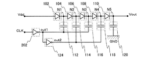
図1に4段の昇圧を行う本発明の昇圧回路の一例を示す。図1(A)において、第1のダイオード102の入力端子の電位は電源電位Vddであり、第1のダイオード102の出力端子には第2のダイオード104の入力端子及び第1の容量素子112の一方の端子が接続されている。同様に、第2のダイオード104の出力端子には第3のダイオード106の入力端子及び第2の容量素子114の一方の端子が接続されている。また、同様に、第3のダイオード106の出力端子には第4のダイオード108の入力端子及び第3の容量素子116の一方の端子が接続されている。以下、同様であるため詳細な説明は省略するが、第nのダイオードの出力端子には第nの容量素子の一方の端子が接続されているということもできる(n:自然数)。また、第n−1のダイオードの出力端子には第nのダイオードの入力端子が接続されている。なお、第5のダイオード110の出力端子は第5の容量素子の一方の端子と接続されており、これが昇圧回路の出力端子Voutとなっている。
FIG. 1 shows an example of a booster circuit according to the present invention for boosting four stages. In FIG. 1A, the potential of the input terminal of the
さらに、第1の容量素子112の他方の端子及び第3の容量素子116の他方の端子は、バッファ回路122の出力端子及びインバータ回路124の入力端子に接続されている。また、第2の容量素子114の他方の端子及び第4の容量素子118の他方の端子は、インバータ回路124の出力端子に接続されている。すなわち、第2k−1の容量素子はバッファ回路122の出力端子及びインバータ回路124の入力端子に接続され、第2kの容量素子はインバータ回路124の出力端子に接続されると考えることができる(k:自然数)。ただし、第5の容量素子120の他方の端子の電位としては接地電位GNDが入力される。バッファ回路122の入力端子にはクロックパルスCLKが入力される。
Further, the other terminal of the
図1(B)は図1(A)におけるバッファ回路122を詳細に見た場合の一例であり、図1(C)は図1(A)におけるインバータ回路124を詳細に見た場合の一例である。
1B is an example when the
バッファ回路122は2段のインバータ回路が直列に接続した構成となっている。具体的には、p型トランジスタ132、142、及びn型トランジスタ134、144により構成されている。ここで、クロックパルスCLKは、p型トランジスタ132のゲート電極及びn型トランジスタ134のゲート電極に入力される。また、p型トランジスタ132のソース電極及びドレイン電極の一方には電源電位Vddとは異なる電源電位V´が入力され、n型トランジスタ134のソース電極及びドレイン電極の一方には接地電位GNDが入力される。そして、p型トランジスタ132のソース電極及びドレイン電極の他方は、n型トランジスタ134のソース電極及びドレイン電極の他方と接続され、次段のインバータ回路を構成するp型トランジスタ142のゲート電極及びn型トランジスタ144のゲート電極に入力される。
The
p型トランジスタ142及びn型トランジスタ144の接続関係については、p型トランジスタ132及びn型トランジスタ134の関係と概ね同様である。p型トランジスタ142のソース電極及びドレイン電極の一方には電源電位Vddとは異なる電源電位V´が入力され、n型トランジスタ144のソース電極及びドレイン電極の一方には接地電位GNDが入力される。そして、p型トランジスタ142のソース電極及びドレイン電極の他方は、n型トランジスタ144のソース電極及びドレイン電極の他方と接続され、出力端子となる。そして、該出力端子からout1が出力される。
The connection relationship between the p-
インバータ回路124は、p型トランジスタ152及びn型トランジスタ154により構成されている。ここで、バッファ回路122の出力端子は、p型トランジスタ152のゲート電極及びn型トランジスタ154のゲート電極に接続される。そして、バッファ回路122の出力out1が、インバータ回路124に入力される。また、p型トランジスタ152のソース電極及びドレイン電極の一方には電源電位Vddとは異なる電源電位V´が入力され、n型トランジスタ154のソース電極及びドレイン電極の一方には接地電位GNDが入力される。そして、p型トランジスタ152のソース電極及びドレイン電極の他方は、n型トランジスタ154のソース電極及びドレイン電極の他方と接続され、インバータ回路の出力端子なる。そして、該出力端子からout2が出力される。
The
ここで重要なのは、バッファ回路122及びインバータ回路124に入力される電源電位V´が電源電位Vddを出力する電源とは異なる電源から出力されるという点である。これにより、昇圧回路を構成する容量素子の充電を、電源電位Vddを出力する電源とは異なる電源の出力により行うことができるため、電源電位Vddの安定化を図ることができる。つまり、電源電位Vddを用いる他の回路を、安定に動作させることができるようになる。なお、上記記載は、電源電位V´が電源電位Vddと等しい構成を除く旨を意図するものではない。
What is important here is that the power supply potential V ′ input to the
以下に、本実施の形態の昇圧回路の動作について説明する。クロックパルスCLKがHighである場合、バッファ回路122のp型トランジスタ132がOFFとなりn型トランジスタ134がONとなるため、p型トランジスタ142及びn型トランジスタ144のゲート電極には接地電位GND、つまりLowが入力される。これにより、バッファ回路122のp型トランジスタ142がONし、n型トランジスタ144がOFFするため、バッファ回路の出力out1は電源電位V´、つまりHighとなる。このとき、インバータ回路124の入力端子がHighであるから、p型トランジスタ152がOFFとなりn型トランジスタ154がONとなるため、インバータ回路の出力out2はLowとなる。反対に、クロックパルスCLKがLowである場合には、バッファ回路の出力out1はLowであり、インバータ回路の出力out2はHighである。
The operation of the booster circuit according to this embodiment will be described below. When the clock pulse CLK is High, the p-
クロックパルスCLKがHighである場合、バッファ回路122の出力out1はHighであるから、第1の容量素子112及び第3の容量素子116が電源電位V´により充電され、ノードN1及びノードN3の電位が所定の値まで引き上げられる。これに伴い、第2のダイオード104及び第4のダイオード108を通じて電荷が流れ、ノードN2及びノードN4の電位が所定の値まで引き上げられる。次にクロックパルスCLKがLowになると、バッファ回路122の出力out1はLowとなり、インバータ回路124の出力out2がHighとなるから、第2の容量素子114及び第4の容量素子118が電源電位V´により充電され、ノードN2及びノードN4の電位がさらに引き上げられる。したがって、ノードN3及びノードN5の電位がさらに引き上げられた値となる。このように、それぞれのノードにおける電位がVN5>VN4>VN3>VN2>VN1>Vddとなることにより、昇圧が行われる。
When the clock pulse CLK is High, since the output out1 of the
なお、図1に示した昇圧回路はバッファ回路122とインバータ回路124を用いる構成としたが、これには限られない。例えば、図2に示す構成とすることもできる。図2の構成は、図1に示す構成のバッファ回路122をインバータ回路202で置き換えたものである。インバータ回路は入力を反転して出力する回路であるから、当該構成を用いても隣接する容量素子に入力されるパルスを反転することが可能であり、昇圧回路として機能させることができる。なお、図2におけるその他の構成は図1に示す構成と同様であるため、図1と同じ符号を用いて表している。
1 is configured to use the
また、図1及び図2に示した昇圧回路は、ダイオードや容量素子を用いる構成であるが、その構成は特に限定されない。例えば、ダイオードとして、トランジスタのソース電極またはドレイン電極の一方をゲート電極と接続した素子を用いても良い。容量素子として、トランジスタのソース電極及びドレイン電極を接続して同電位とした構成の素子を用いても良い。また、図1及び図2に示した昇圧回路は4段の昇圧を行うものであるが、これに限られるのもではない。要求される昇圧の程度に合わせて、適宜、段数を変更することが好ましい。 The booster circuit shown in FIGS. 1 and 2 has a configuration using a diode or a capacitor, but the configuration is not particularly limited. For example, an element in which one of a source electrode and a drain electrode of a transistor is connected to a gate electrode may be used as the diode. As the capacitor, an element having a structure in which the source electrode and the drain electrode of the transistor are connected to have the same potential may be used. Further, the booster circuit shown in FIGS. 1 and 2 performs four-stage boosting, but is not limited thereto. It is preferable to change the number of stages as appropriate in accordance with the required degree of boosting.
本実施の形態に示す昇圧回路は、容量素子の充電に電源電位Vddを用いない構成をとる。これにより、昇圧回路の動作に起因する電源電位Vddの変動を抑えることができる。したがって、他の回路に供給する電力の安定化を図ることができ、他の回路の動作不良を低減することができる。 The booster circuit described in this embodiment has a structure in which the power supply potential Vdd is not used for charging the capacitor. Thereby, fluctuations in the power supply potential Vdd caused by the operation of the booster circuit can be suppressed. Therefore, it is possible to stabilize the power supplied to the other circuits, and to reduce malfunctions of the other circuits.
なお、本実施の形態に示した昇圧回路はあくまでも一例に過ぎず、その構成は、本実施の形態に限定されるものではない。 Note that the booster circuit described in this embodiment is merely an example, and the structure thereof is not limited to this embodiment.
(実施の形態2)
本実施の形態では、実施の形態1に示した昇圧回路の変形例について図3を用いて以下に説明する。
(Embodiment 2)
In this embodiment, a modification of the booster circuit described in
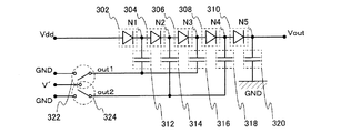
図3は、4段の昇圧を行う本発明の昇圧回路の別の一例である。図3において、第1のダイオード302の入力端子の電位は電源電位Vddであり、第1のダイオード302の出力端子には第2のダイオード304の入力端子及び第1の容量素子312の一方の端子が接続されている。同様に、第2のダイオード304の出力端子には第3のダイオード306の入力端子及び第2の容量素子314の一方の端子が接続されている。以下、同様であるため詳細な説明は省略するが、第nのダイオードの出力端子には第nの容量素子の一方の端子が接続されているということもできる(n:自然数)。また、第n−1のダイオードの出力端子には第nのダイオードの入力端子が接続されている。なお、第5のダイオード310の出力端子は第5の容量素子の一方の端子と接続されており、これが昇圧回路の出力端子Voutとなっている。
FIG. 3 shows another example of the booster circuit of the present invention that performs boosting in four stages. In FIG. 3, the potential of the input terminal of the
また、第1の容量素子312の他方の端子及び第3の容量素子316の他方の端子は、第1のスイッチ素子322に接続されている。また、第2の容量素子314の他方の端子及び第4の容量素子318の他方の端子は、第2のスイッチ素子324に接続されている。すなわち、第2k−1の容量素子は第1のスイッチ素子322に接続され、第2kの容量素子は第2のスイッチ素子324に接続されると考えることができる(k:自然数)。ただし、第5の容量素子320の他方の端子の電位としては接地電位GNDが入力される。
The other terminal of the
本実施の形態の昇圧回路は、バッファ回路及びインバータ回路をより一般的なスイッチ素子に置き換えた点で実施の形態1に示した昇圧回路と異なる。ここで、第1のスイッチ素子322及び第2のスイッチ素子324は共に、電源電位V´又は接地電位GNDを選択するための素子である。
The booster circuit of the present embodiment is different from the booster circuit shown in the first embodiment in that the buffer circuit and the inverter circuit are replaced with more general switch elements. Here, both the
以下に、本実施の形態の昇圧回路の動作について説明する。まず、第1のスイッチ素子322及び第2のスイッチ素子324の一方が電源電位V´を選択するように、他方が接地電位GNDを選択するようにする。例えば、第1のスイッチ素子322が電源電位V´を選択し、第2のスイッチ素子324が接地電位GNDを選択した場合を考える。このとき、第1の容量素子312及び第3の容量素子316が電源電位V´により充電され、ノードN1及びノードN3の電位が所定の値まで引き上げられる。これに伴い、第2のダイオード304及び第4のダイオード308を通じて電荷が流れ、ノードN2及びノードN4の電位が所定の値まで引き上げられる。
The operation of the booster circuit according to this embodiment will be described below. First, one of the
次に、第1のスイッチ素子及び第2のスイッチ素子を切り替えて、第1のスイッチ素子322及び第2のスイッチ素子324の一方が接地電位GNDを選択するように、他方が電源電位V´を選択するようにする。つまり、第1のスイッチ素子322が接地電位GNDを選択し、第2のスイッチ素子324が電源電位V´を選択する。このとき、第2の容量素子114及び第4の容量素子118が電源電位V´により充電され、ノードN2及びノードN4の電位がさらに引き上げられる。したがって、ノードN3及びノードN5の電位がさらに引き上げられた値となる。このように、それぞれのノードにおける電位がVN5>VN4>VN3>VN2>VN1>Vddとなることにより、昇圧が行われる。
Next, the first switch element and the second switch element are switched so that one of the
ただし、スイッチ素子の切り替えは、それぞれの容量素子が完全に放電する前に行わなくてはならない。完全に放電した場合には、ノードの電位を引き上げる効果が得られなくなってしまうためである。 However, the switching of the switching elements must be performed before each capacitive element is completely discharged. This is because the effect of raising the potential of the node cannot be obtained when it is completely discharged.
本実施の形態に示す昇圧回路は、容量素子の充電に電源電位Vddを用いない構成をとる。これにより、昇圧回路の動作に起因する電源電位Vddの変動を抑えることができる。このため、他の回路に供給する電力の安定化を図ることができ、他の回路の動作不良を低減することができる。本発明の効果は、昇圧回路の容量素子を充電するための電位を別系統とすることにより得られるものである。従って、昇圧回路の構成としては特に限定されず、本実施の形態のように、バッファ回路やインバータ回路を用いない構成としても良い。スイッチ素子の構成についても、適宜変更することができる。また、図3に示した昇圧回路は4段の昇圧を行うものであるが、これに限られるものではない。要求される昇圧の程度に合わせて、適宜、段数を変更することが好ましい。 The booster circuit described in this embodiment has a structure in which the power supply potential Vdd is not used for charging the capacitor. Thereby, fluctuations in the power supply potential Vdd caused by the operation of the booster circuit can be suppressed. For this reason, it is possible to stabilize the power supplied to other circuits, and to reduce malfunctions of other circuits. The effect of the present invention can be obtained by setting the potential for charging the capacitive element of the booster circuit to be a separate system. Therefore, the configuration of the booster circuit is not particularly limited, and a configuration without using a buffer circuit or an inverter circuit may be used as in this embodiment. The configuration of the switch element can also be changed as appropriate. Further, the booster circuit shown in FIG. 3 performs boosting in four stages, but is not limited to this. It is preferable to change the number of stages as appropriate in accordance with the required degree of boosting.
なお、本実施の形態に示した昇圧回路はあくまでも一例に過ぎず、その構成は、本実施の形態に限定されるものではない。 Note that the booster circuit described in this embodiment is merely an example, and the structure thereof is not limited to this embodiment.
(実施の形態3)
本実施の形態では、本発明の昇圧回路を用いた半導体装置について図4及び5を用いて以下に説明する。
(Embodiment 3)
In this embodiment mode, a semiconductor device using the booster circuit of the present invention will be described below with reference to FIGS.
図4(A)は、本発明の昇圧回路を用いた半導体装置の構成の一例である。アンテナ402が電源回路404の入力端子及び充電回路416の入力端子に接続されている。電源回路404の出力端子は定電圧回路406の入力端子に接続され、また、定電圧回路406の出力端子は昇圧回路408の入力端子、ロジック回路410、アナログ回路412に接続されている。充電回路416の出力端子は二次電池418に接続され、二次電池418は昇圧回路408に接続され、昇圧回路408の出力端子はメモリ回路414に接続されている。ここで、昇圧回路408は、定電圧回路406の出力端子からの電圧を、二次電池から供給される電力によって昇圧する構成を有する。
FIG. 4A illustrates an example of a structure of a semiconductor device using the booster circuit of the present invention. The
なお、図4に示す構成は電力の流れを明確にするための模式図であり、図4に示した接続関係以外にも複数の接続関係が存在している。例えば、メモリ回路と、ロジック回路またはアナログ回路の間には、データのやり取りを行うための配線が接続されている。また、昇圧回路408にはアンテナからの信号に基づいて生成されたクロックパルスが供給される。
The configuration shown in FIG. 4 is a schematic diagram for clarifying the flow of power, and there are a plurality of connection relationships in addition to the connection relationship shown in FIG. For example, wiring for exchanging data is connected between a memory circuit and a logic circuit or an analog circuit. The
ここで、充電回路を用いて二次電池を充電する構成について詳細に説明する。 Here, the structure which charges a secondary battery using a charging circuit is demonstrated in detail.
図4(B)に示すように、本実施の形態において説明する充電回路416は、整流回路422、電圧制御回路424、スイッチ素子A426、および、充電制御回路428を有する。アンテナ402が整流回路422の入力端子に接続され、整流回路422の出力端子は電圧制御回路424の入力端子に接続される。また、電圧制御回路424の出力端子は、スイッチ素子A426を介して二次電池418に接続される。充電制御回路428は、二次電池418と接続してその充電状況をモニタし、それに応じてスイッチ素子A426のON/OFFを制御する。
As shown in FIG. 4B, a charging
スイッチ素子A426としてダイオードを用いることにより、充電制御回路428を省略する構成とすることができる。また、電圧制御回路424は、電圧および電流の制御回路であってもよい。
By using a diode as the switch element A426, the
次に、半導体装置と通信を行い、二次電池を充電することが可能なリーダライタの例を図4(C)に示す。リーダライタは、制御系432、および、アンテナ434を有する。
Next, FIG. 4C illustrates an example of a reader / writer that can communicate with a semiconductor device and charge a secondary battery. The reader / writer has a
リーダライタから半導体装置の二次電池を充電する最も簡単な例としては、図5(A)に示すように、振幅が等しい電磁波500を用いて通信する場合である。この時の充電方法を図5(B)のフローチャートで示す。
The simplest example of charging a secondary battery of a semiconductor device from a reader / writer is a case where communication is performed using an
初めに、ステップS502として、充電器のアンテナから振幅の等しい電磁波の送信を開始する。ステップS504としてRFIDタグが電磁波を受信すると、ステップS506として、スイッチA(SWA)がONとなり、二次電池への充電が開始される。このとき、ステップS508として充電制御回路は二次電池への充電状況を監視する。二次電池の電圧が一定値以上になると(YES)、ステップS510として、RFIDタグは充電が終了したことを伝える信号を送信する。ステップS512として、その信号を受信したリーダライタは、ステップS514として、電磁波の送信を停止する。なお、二次電池の電圧が一定値に達していない場合(NO)には、ステップS506に戻り、そのまま充電を行う。 First, in step S502, transmission of electromagnetic waves having the same amplitude from the antenna of the charger is started. When the RFID tag receives an electromagnetic wave in step S504, in step S506, the switch A (SWA) is turned on and charging of the secondary battery is started. At this time, as step S508, the charging control circuit monitors the charging state of the secondary battery. When the voltage of the secondary battery becomes equal to or higher than a certain value (YES), the RFID tag transmits a signal notifying that the charging is finished as step S510. In step S512, the reader / writer that has received the signal stops transmitting electromagnetic waves in step S514. If the voltage of the secondary battery has not reached a certain value (NO), the process returns to step S506 and charging is performed as it is.
なお、本実施の形態に示す構成においては、ロジック回路等が動作するタイミングにおいて、二次電池の充電を行わないようにすることが好ましい。二次電池の充電を行うことにより、ロジック回路等に供給される電力が不安定になる可能性が高いためである。 Note that in the structure described in this embodiment, it is preferable not to charge the secondary battery at a timing when the logic circuit or the like operates. This is because the power supplied to the logic circuit or the like is likely to become unstable by charging the secondary battery.
本発明の昇圧回路を用いて半導体装置を作製することにより、アンテナから供給される電力の安定化を図ることができる。特に、データの書込み時に高電圧を要する不揮発性メモリを用いる場合には、その効果は著しく、他の回路の動作不良を大幅に低減することができる。また、半導体装置外部への応答出力が低下することを防止できる。すなわち、通信距離を向上することができる。また、アンテナから供給される電力を用いる場合と比較して大きな電力を用いることができるため、昇圧回路の昇圧能力を向上することができる。 By manufacturing a semiconductor device using the booster circuit of the present invention, power supplied from an antenna can be stabilized. In particular, when a non-volatile memory that requires a high voltage at the time of data writing is used, the effect is remarkable, and malfunctions of other circuits can be greatly reduced. Further, it is possible to prevent the response output to the outside of the semiconductor device from being lowered. That is, the communication distance can be improved. In addition, since a large amount of power can be used as compared with the case where the power supplied from the antenna is used, the boosting capability of the booster circuit can be improved.
さらに、二次電池の電源電位の低下は極わずかであり、昇圧回路を構成する容量素子の充電を高速に行うことができるため、昇圧時間を短縮することができる。また、昇圧回路への電力供給を別系統とすることにより、他の回路に要求される電力の条件を緩和することができるため、他の回路の規模を拡大することが可能となる。また、電源に起因するノイズを低減することもできる。また、無線によって充電可能な二次電池を用いることにより、煩雑な充電作業が不要になる。また、一次電池を用いる場合と比較して、経時的な劣化は極わずかであり、電池の交換作業も不要である。 Further, the decrease in the power supply potential of the secondary battery is negligible, and the capacitor element constituting the booster circuit can be charged at high speed, so that the boosting time can be shortened. In addition, since the power supply to the booster circuit is made a separate system, the power condition required for the other circuit can be relaxed, so that the scale of the other circuit can be increased. In addition, noise caused by the power source can be reduced. In addition, the use of a rechargeable secondary battery eliminates the need for complicated charging operations. Moreover, compared with the case where a primary battery is used, deterioration with time is very small, and battery replacement work is not necessary.
本実施の形態において充電回路416をアンテナ402に接続する構成を示したが、当該構成はあくまでも一例に過ぎず、本発明は本実施の形態に限定されるものではない。例えば、充電回路が、電源回路や定電圧回路を介してアンテナに接続される構成であってもよい。この場合には、充電回路の構成も適宜変更することが好ましい。また、昇圧回路に入力される二次電池の出力をコントロールする手段を有していても良い。当該手段を有することにより、回路構成を変更することなく、昇圧回路の出力電圧をコントロールすることができる。また、昇圧回路の電力供給先はメモリ回路に限られず、その他の回路としても良い。
Although the structure in which the
また、本実施の形態にて示した半導体装置は、ロジック回路、アナログ回路等への電力供給を電源回路及び定電圧回路を介して行う構成としたが、これに限られるものではない。たとえば、電源回路404及び定電圧回路406に代えて充電回路及び二次電池を用いる構成としても良い。このような構成とすることによって、ロジック回路やアナログ回路を二次電池から供給される電力にて動作させることができるため、二次電池を用いない場合と比較して動作の安定性を向上できる。なお、上記充電回路及び二次電池への置換は、実施の形態1及び実施の形態2に示した昇圧回路の電位Vddを二次電池の電位V´´に置き換えることに等しい。もちろん、結果として、V´´=Vdd、又は、V´´=V´となることを妨げるものではない。
In the semiconductor device described in this embodiment, power is supplied to a logic circuit, an analog circuit, and the like through a power supply circuit and a constant voltage circuit; however, the present invention is not limited to this. For example, instead of the
また、昇圧回路に供給される電力の全てを、二次電池418から供給する構成とすることもできる。これは、実施の形態1及び実施の形態2に示した昇圧回路の電位Vddを電位V´に置き換えることに等しい。当該構成とすることによって、充電回路及び二次電池を複数設ける必要がないため、回路構成を簡略化することができる。本実施の形態は、実施の形態1または2と適宜組み合わせることができる。
Further, all the power supplied to the booster circuit can be supplied from the
(実施の形態4)
本実施の形態では、本発明の昇圧回路を用いた半導体装置についての別の例を、図6を用いて以下に説明する。
(Embodiment 4)
In this embodiment mode, another example of a semiconductor device using the booster circuit of the present invention will be described below with reference to FIGS.
図6は、本発明の昇圧回路を用いた半導体装置の構成の別の一例である。アンテナ602が電源回路604の入力端子に接続されている。電源回路604の出力端子は定電圧回路606の入力端子に接続され、また、定電圧回路606の出力端子は昇圧回路618の入力端子、ロジック回路608、アナログ回路610に接続されている。さらに、アンテナ602とは異なるアンテナ612が充電回路614の入力端子に接続されている。充電回路614の出力端子は二次電池616に接続され、二次電池616は昇圧回路618に接続され、昇圧回路618の出力端子はメモリ回路620に接続されている。ここで、昇圧回路618は、定電圧回路606の出力端子からの電圧を、二次電池616から供給される電力によって昇圧する構成を有する。
FIG. 6 shows another example of the configuration of the semiconductor device using the booster circuit of the present invention. An
なお、図6に示す構成は電力の流れを明確にするための模式図であり、図6に示した接続関係以外にも複数の接続関係が存在している。例えば、メモリ回路と、ロジック回路またはアナログ回路の間には、データのやり取りを行うための配線が接続されている。また、昇圧回路618にはアンテナからの信号に基づいて生成されたクロックパルスが供給される。
The configuration shown in FIG. 6 is a schematic diagram for clarifying the flow of power, and there are a plurality of connection relationships in addition to the connection relationship shown in FIG. For example, wiring for exchanging data is connected between a memory circuit and a logic circuit or an analog circuit. The
本実施の形態の半導体装置が実施の形態3に示す半導体装置と異なる点は、昇圧に用いる電力を発生するアンテナ612が、ロジック回路等に電力を供給するアンテナ602とは別に存在している点である。
The semiconductor device of this embodiment is different from the semiconductor device described in Embodiment 3 in that an
次に、本実施の形態において、充電回路を用いて二次電池を充電するための構成について説明する。 Next, a configuration for charging a secondary battery using a charging circuit in the present embodiment will be described.
図6(B)に示すように、本実施の形態にて説明する充電回路614は、整流回路622、電圧制御回路624、スイッチ素子A626、および、充電制御回路628を有する。アンテナ612が整流回路622の入力端子に接続され、整流回路622の出力端子は電圧制御回路624の入力端子に接続される。また、電圧制御回路624の出力端子は、スイッチ素子A626を介して二次電池616に接続される。充電制御回路628は、二次電池616と接続してその充電状況をモニタし、それに応じてスイッチ素子A626のON/OFFを制御する。
As shown in FIG. 6B, a charging
スイッチ素子A626としてダイオードを用いることにより、充電制御回路628を省略する構成とすることができる。また、電圧制御回路624は、電圧および電流の制御回路であってもよい。
By using a diode as the
リーダライタから半導体装置の二次電池を充電する例としては、実施の形態3にて説明した方法などを適宜用いることができるため、ここでは省略する。 As an example of charging the secondary battery of the semiconductor device from the reader / writer, the method described in Embodiment Mode 3 or the like can be used as appropriate, and thus description thereof is omitted here.
本発明の昇圧回路を用いて半導体装置を作製することにより、アンテナから供給される電力の安定化を図ることができる。これにより、他の回路の動作不良を低減することができる。また、半導体装置外部への応答出力が低下することを防止できる。すなわち、通信距離を向上することができる。また、アンテナから供給される電力を用いる場合と比較して大きな電力を用いることができるため、昇圧回路の昇圧能力を向上することができる。なお、本実施の形態に示すように、昇圧用の電源を供給するためのアンテナを別系統とすることにより、ロジック回路等の動作に関わり無く、常に二次電池の充電を行うことができる。したがって、充電の効率を高めることが出来る。 By manufacturing a semiconductor device using the booster circuit of the present invention, power supplied from an antenna can be stabilized. As a result, malfunction of other circuits can be reduced. Further, it is possible to prevent the response output to the outside of the semiconductor device from being lowered. That is, the communication distance can be improved. In addition, since a large amount of power can be used as compared with the case where the power supplied from the antenna is used, the boosting capability of the booster circuit can be improved. Note that as shown in this embodiment mode, by using a separate antenna for supplying power for boosting, the secondary battery can be always charged regardless of the operation of the logic circuit or the like. Therefore, the charging efficiency can be increased.
さらに、二次電池の電源電位の低下は極わずかであり、昇圧回路を構成する容量素子の充電を高速に行うことができるため、昇圧時間を短縮することができる。また、昇圧回路への電力供給を別系統とすることにより、他の回路に要求される電力の条件を緩和することができるため、他の回路の規模を拡大することが可能となる。また、電源に起因するノイズを低減することもできる。また、無線によって充電可能な二次電池を用いることにより、煩雑な充電作業が不要になる。また、一次電池を用いる場合と比較して、経時的な劣化は極わずかであり、電池の交換作業も不要である。 Further, the decrease in the power supply potential of the secondary battery is negligible, and the capacitor element constituting the booster circuit can be charged at high speed, so that the boosting time can be shortened. In addition, since the power supply to the booster circuit is made a separate system, the power condition required for the other circuit can be relaxed, so that the scale of the other circuit can be increased. In addition, noise caused by the power source can be reduced. In addition, the use of a rechargeable secondary battery eliminates the need for complicated charging operations. Moreover, compared with the case where a primary battery is used, deterioration with time is very small, and battery replacement work is not necessary.
本実施の形態において示した構成はあくまでも一例に過ぎず、本発明は本実施の形態に限定されるものではない。本実施の形態は、実施の形態1乃至3と適宜組み合わせることができる。
The configuration shown in the present embodiment is merely an example, and the present invention is not limited to the present embodiment. This embodiment mode can be combined with any of
(実施の形態5)
本実施の形態では、本発明の昇圧回路を用いた半導体装置についての別の例を、図7を用いて以下に説明する。
(Embodiment 5)
In this embodiment mode, another example of a semiconductor device using the booster circuit of the present invention will be described below with reference to FIGS.
図7(A)は、本発明の昇圧回路を用いた半導体装置の構成の別の一例である。図7(A)において、アンテナ702が電源回路704の入力端子、充電回路A712の入力端子、及び充電回路B716の入力端子に接続されている。電源回路704の出力端子は定電圧回路706の入力端子に接続され、また、定電圧回路706の出力端子は昇圧回路720の入力端子、ロジック回路708、アナログ回路710に接続されている。さらに、充電回路A712の出力端子は二次電池A714に接続され、充電回路B716の出力端子は二次電池B718に接続されている。二次電池A714及び二次電池B718は昇圧回路720に接続され、昇圧回路720の出力端子はメモリ回路722に接続されている。ここで、昇圧回路720は、定電圧回路706の出力端子からの電圧を、二次電池A714及び二次電池B718から供給される電力によって昇圧する構成を有する。
FIG. 7A illustrates another example of a structure of a semiconductor device using the booster circuit of the present invention. In FIG. 7A, an
なお、図7(A)に示す構成は電力の流れを明確にするための模式図であり、図7(A)に示した接続関係以外にも複数の接続関係が存在している。例えば、メモリ回路と、ロジック回路またはアナログ回路の間には、データのやり取りを行うための配線が接続されている。また、昇圧回路720にはアンテナからの信号に基づいて生成されたクロックパルスが供給される。
Note that the structure illustrated in FIG. 7A is a schematic diagram for clarifying the flow of power, and there are a plurality of connection relationships in addition to the connection relationship illustrated in FIG. For example, wiring for exchanging data is connected between a memory circuit and a logic circuit or an analog circuit. The
図7(A)に示す半導体装置が実施の形態3に示す半導体装置と異なる点は、昇圧に用いる電力を発生するアンテナ702が、二つの充電回路に接続され、当該二つの充電回路がそれぞれ対応する二次電池を充電する点である。当該構成を用いて、例えば、二つの二次電池の電力が、昇圧回路のバッファ回路とインバータ回路にそれぞれ供給される構成とすることができる。
The semiconductor device illustrated in FIG. 7A is different from the semiconductor device described in Embodiment 3 in that an
図7(B)は、本発明の昇圧回路を用いた半導体装置の構成のさらに別の例である。アンテナ752が電源回路754の入力端子に接続されている。電源回路754の出力端子は定電圧回路756の入力端子に接続され、また、定電圧回路756の出力端子は昇圧回路772の入力端子、ロジック回路758、アナログ回路760に接続されている。さらに、アンテナ752とは異なるアンテナ762が、充電回路A764の入力端子及び充電回路B768の入力端子に接続されている。充電回路A764の出力端子は二次電池A766に接続され、充電回路B768の出力端子は二次電池B770に接続され、二次電池A766及び二次電池B770は昇圧回路772に接続され、昇圧回路772の出力端子はメモリ回路774に接続されている。ここで、昇圧回路772は、定電圧回路756の出力端子からの電圧を、二次電池A766及び二次電池B770から供給される電力によって昇圧する構成を有する。
FIG. 7B shows still another example of the structure of the semiconductor device using the booster circuit of the present invention. An
なお、図7(B)に示す構成は電力の流れを明確にするための模式図であり、図7(B)に示した接続関係以外にも複数の接続関係が存在している。例えば、メモリ回路と、ロジック回路またはアナログ回路の間には、データのやり取りを行うための配線が接続されている。また、昇圧回路772にはアンテナからの信号に基づいて生成されたクロックパルスが供給される。
Note that the structure illustrated in FIG. 7B is a schematic diagram for clarifying the flow of power, and there are a plurality of connection relationships in addition to the connection relationship illustrated in FIG. For example, wiring for exchanging data is connected between a memory circuit and a logic circuit or an analog circuit. The
図7(B)に示す半導体装置が実施の形態3に示す半導体装置と異なる点は、昇圧に用いる電力を発生するアンテナ762が、ロジック回路等に電力を供給するアンテナ752とは別に存在している点、及び、昇圧に用いる電力を発生するアンテナ762が、二つの充電回路に接続され、当該二つの充電回路がそれぞれ二つの二次電池を充電する点である。当該構成を用いて、例えば、二つの二次電池の電力が、昇圧回路のバッファ回路とインバータ回路にそれぞれ供給される構成とすることができる。
The semiconductor device illustrated in FIG. 7B is different from the semiconductor device described in Embodiment 3 in that an
充電回路の具体的な構成については、実施の形態3又は4にて示した構成などを適宜用いることができるため、ここでは省略する。また、リーダライタから半導体装置の二次電池を充電する例としては、実施の形態3にて説明した方法などを適宜用いることができる。 The specific structure of the charging circuit is not described here because the structure described in Embodiment 3 or 4 can be used as appropriate. As an example of charging the secondary battery of the semiconductor device from the reader / writer, the method described in Embodiment 3 can be used as appropriate.
本実施の形態にて示した構成を用いて半導体装置を作製する場合、アンテナから供給される電力の安定化を図ることができる。これにより、他の回路の動作不良を低減することができる。また、半導体装置外部への応答出力が低下することを防止できる。すなわち、通信距離を向上することができる。また、アンテナから供給される電力を用いる場合と比較して大きな電力を用いることができるため、昇圧回路の昇圧能力を向上することができる。さらに、個々の二次電池への負荷を低減することができるため、電力の安定化等の観点から好ましい。また、二次電池の電源電位の低下は極わずかであり、昇圧回路を構成する容量素子の充電を高速に行うことができるため、昇圧時間を短縮することができる。 In the case where a semiconductor device is manufactured using the structure described in this embodiment, power supplied from an antenna can be stabilized. As a result, malfunction of other circuits can be reduced. Further, it is possible to prevent the response output to the outside of the semiconductor device from being lowered. That is, the communication distance can be improved. In addition, since a large amount of power can be used as compared with the case where the power supplied from the antenna is used, the boosting capability of the booster circuit can be improved. Furthermore, since the load to each secondary battery can be reduced, it is preferable from the viewpoint of power stabilization and the like. In addition, since the power supply potential of the secondary battery is extremely low, the capacitor element constituting the booster circuit can be charged at high speed, so that the boosting time can be shortened.
図7(B)の構成を用いて半導体装置を作製した場合、昇圧用の電源を供給するためのアンテナを別系統とすることができる。これにより、ロジック回路等の動作に関わり無く、常に二次電池の充電を行うことができる。したがって、充電の効率を高めることが出来る。また、昇圧回路への電力供給を別系統とすることにより、他の回路に要求される電力の条件を緩和することができるため、他の回路の規模を拡大することが可能となる。また、電源に起因するノイズを低減することもできる。また、無線によって充電可能な二次電池を用いることにより、煩雑な充電作業が不要になる。また、一次電池を用いる場合と比較して、経時的な劣化は極わずかであり、電池の交換作業も不要である。 In the case where a semiconductor device is manufactured using the structure in FIG. 7B, an antenna for supplying power for boosting can be provided as a separate system. As a result, the secondary battery can always be charged regardless of the operation of the logic circuit or the like. Therefore, the charging efficiency can be increased. In addition, since the power supply to the booster circuit is made a separate system, the power condition required for the other circuit can be relaxed, so that the scale of the other circuit can be increased. In addition, noise caused by the power source can be reduced. In addition, the use of a rechargeable secondary battery eliminates the need for complicated charging operations. Moreover, compared with the case where a primary battery is used, deterioration with time is very small, and battery replacement work is not necessary.
本実施の形態において示した構成はあくまでも一例に過ぎず、本発明は本実施の形態に限定されるものではない。例えば、図7(A)において、充電回路A及び充電回路Bは、電源回路や定電圧回路を介してアンテナに接続されていてもよい。この場合には、充電回路A及び充電回路Bの構成も適宜変更することが好ましい。また、充電回路Aと充電回路Bの機能をまとめて一つの充電回路としても良い。本実施の形態は、実施の形態1乃至4と適宜組み合わせることができる。
The configuration shown in the present embodiment is merely an example, and the present invention is not limited to the present embodiment. For example, in FIG. 7A, the charging circuit A and the charging circuit B may be connected to the antenna via a power supply circuit or a constant voltage circuit. In this case, it is preferable to appropriately change the configuration of the charging circuit A and the charging circuit B. Further, the functions of the charging circuit A and the charging circuit B may be integrated into one charging circuit. This embodiment can be combined with any of
(実施の形態6)
本実施の形態では、上記実施の形態にて示した半導体装置の作製方法の一例について、図8乃至12を参照して説明する。
(Embodiment 6)
In this embodiment, an example of a method for manufacturing the semiconductor device described in the above embodiment will be described with reference to FIGS.
まず、基板801の一表面に絶縁膜802を介して剥離層803を形成し、続けて下地膜として機能する絶縁膜804と半導体膜805(例えば、非晶質珪素を含む膜)を積層して形成する(図8(A)参照)。なお、絶縁膜802、剥離層803、絶縁膜804および半導体膜805は、連続して形成することができる。
First, a
なお、基板801は、ガラス基板、石英基板、セラミック基板、金属基板(例えば、ステンレス基板など)、Si基板等から選択されるものである。他にも、プラスチック基板である、ポリエチレンテレフタレート(PET)、ポリエチレンナフタレート(PEN)、ポリエーテルサルフォン(PES)、アクリルなどの基板を選択することもできる。なお、本工程では、剥離層803は、絶縁膜802を介して基板801の全面に設けているが、フォトリソグラフィ法を用いてマスクを形成し、エッチングを行うことにより、選択的に形成してもよい。
The
また、絶縁膜802、絶縁膜804は、CVD法やスパッタリング法等を用いて、酸化シリコン、窒化シリコン、酸化窒化シリコン(SiOxNy:x>y>0)、窒化酸化シリコン(SiNxOy:x>y>0)等の絶縁材料を用いて形成することができる。例えば、絶縁膜802、804をそれぞれ2層構造として、第1層目の絶縁膜として窒化酸化シリコン膜を、第2層目の絶縁膜として酸化窒化シリコン膜を形成することができる。また、第1層目の絶縁膜として窒化シリコン膜を形成し、第2層目の絶縁膜として酸化シリコン膜を形成してもよい。もちろん、単層構造であっても良いし、3層以上の積層構造とすることも可能である。絶縁膜802は、基板801から、剥離層803又はその上に形成される素子に不純物元素が混入するのを防ぐブロッキング層として機能し、絶縁膜804は基板801、剥離層803から、その上に形成される素子に不純物元素が混入するのを防ぐブロッキング層として機能する。このように、ブロッキング層として機能する絶縁膜802、804を形成することによって、基板801からのNaなどのアルカリ金属やアルカリ土類金属が、素子に侵入して悪影響を及ぼすことを防ぐことができ、また、剥離層803からの不純物元素が、素子に侵入して悪影響を及ぼすことを防ぐことができる。なお、基板801として石英基板のように不純物元素の影響を無視できる基板を用いる場合には絶縁膜802、804を省略してもよい。
The insulating
また、剥離層803には、金属膜や、金属膜と金属酸化膜の積層構造等を用いることができる。上記金属膜の材料としては、タングステン(W)、モリブデン(Mo)、チタン(Ti)、タンタル(Ta)、ニオブ(Nb)、ニッケル(Ni)、コバルト(Co)、ジルコニウム(Zr)、亜鉛(Zn)、ルテニウム(Ru)、ロジウム(Rh)、パラジウム(Pd)、オスミウム(Os)、イリジウム(Ir)から選択された元素または当該元素を主成分とする合金材料若しくは化合物材料が挙げられる。当該材料を用いて単層構造又は積層構造の金属膜を形成することができる。なお、金属膜の形成方法として、スパッタ法や、プラズマCVD法等の各種CVD法等を用いることができる。金属膜と金属酸化膜の積層構造としては、上述した金属膜を形成した後に、酸素雰囲気下又はN2O雰囲気下におけるプラズマ処理や、酸素雰囲気下又はN2O雰囲気下における加熱処理等を行うことによって、金属膜表面に当該金属膜の酸化膜又は酸化窒化膜を形成した構造を用いることができる。例えば、金属膜としてスパッタ法やCVD法等によりタングステン膜を設けた場合、酸素雰囲気下においてタングステン膜にプラズマ処理を行うことで、タングステン膜表面にタングステン酸化物からなる金属酸化膜を形成することができる。この場合、タングステンの酸化物は、WOxで表され、Xは2乃至3であり、Xが2の場合(WO2)、Xが2.5の場合(W2O5)、Xが2.75の場合(W4O11)、Xが3の場合(WO3)などがある。タングステンの酸化物を形成するにあたり、上記に挙げたXの値に特に制約はなく、エッチングレート等を基に、その構成を決定すれば良い。
For the
半導体膜805は、スパッタリング法、LPCVD法、プラズマCVD法等により、25nm以上200nm以下(好ましくは30nm以上150nm以下)の厚さで形成する。半導体膜805の材料に限定はないが、好ましくはシリコンまたはシリコンゲルマニウムを用いると良い。
The
次に、半導体膜805にレーザー光を照射して結晶化を行う。なお、レーザー光の照射に、RTA又はファーネスアニール炉を用いる熱結晶化法や、結晶化を助長する金属元素を用いる熱結晶化法等を組み合わせた方法を用いて、半導体膜805の結晶化を行ってもよい。その後、得られた結晶質半導体膜を所望の形状にエッチングして、結晶化した半導体膜805a〜805fを形成し、当該半導体膜805a〜805fを覆うようにゲート絶縁膜806を形成する(図8(B)参照)。
Next, crystallization is performed by irradiating the
ここで、結晶化に用いるレーザービームとしては、連続発振(CW:continuous−wave)型のレーザービームやパルス発振型のレーザービーム(パルスレーザービーム)を用いることができる。例えば、Arレーザー、Krレーザー、エキシマレーザーなどの気体レーザー、単結晶のYAG、YVO4、フォルステライト(Mg2SiO4)、YAlO3、GdVO4、若しくは多結晶(セラミック)のYAG、Y2O3、YVO4、YAlO3、GdVO4などに、ドーパントとしてNd、Yb、Cr、Ti、Ho、Er、Tm、Taのうち1種または複数種が添加された材料を媒質とするレーザー、ガラスレーザー、ルビーレーザー、アレキサンドライトレーザー、Ti:サファイアレーザー、銅蒸気レーザーまたは金蒸気レーザーなどから発振されるものを用いることができる。このようなレーザービームの基本波、及び基本波の第2高調波、第3高調波、第4高調波を照射することで、大粒径の結晶を得ることができる。例えば、Nd:YVO4レーザー(基本波1064nm)の第2高調波(532nm)や第3高調波(355nm)を用いることができる。上記Nd:YVO4レーザーは、連続発振で射出することも、パルス発振で射出することも可能である。 Here, as a laser beam used for crystallization, a continuous-wave (CW) laser beam or a pulsed laser beam (pulse laser beam) can be used. For example, gas laser such as Ar laser, Kr laser, excimer laser, single crystal YAG, YVO 4 , forsterite (Mg 2 SiO 4 ), YAlO 3 , GdVO 4 , or polycrystalline (ceramic) YAG, Y 2 O 3 , YVO 4 , YAlO 3 , GdVO 4, etc., and a laser, glass laser using a material containing one or more of Nd, Yb, Cr, Ti, Ho, Er, Tm, Ta as dopants , Lasers emitted from ruby laser, alexandrite laser, Ti: sapphire laser, copper vapor laser, gold vapor laser, or the like can be used. By irradiating the fundamental wave of such a laser beam and the second, third and fourth harmonics of the fundamental wave, a crystal having a large grain size can be obtained. For example, the second harmonic (532 nm) or the third harmonic (355 nm) of an Nd: YVO 4 laser (fundamental wave 1064 nm) can be used. The Nd: YVO 4 laser can be emitted by continuous oscillation or pulse oscillation.
なお、単結晶のYAG、YVO4、フォルステライト(Mg2SiO4)、YAlO3、GdVO4、若しくは多結晶(セラミック)のYAG、Y2O3、YVO4、YAlO3、GdVO4などに、ドーパントとしてNd、Yb、Cr、Ti、Ho、Er、Tm、Taのうち1種または複数種が添加された材料を媒質とするレーザー、Arイオンレーザー、またはTi:サファイアレーザーは、連続発振をさせることが可能であり、Qスイッチ動作やモード同期などを行うことによって10MHz以上の発振周波数でパルス発振をさせることも可能である。10MHz以上の発振周波数でレーザービームを発振させると、半導体膜がレーザーによって溶融してから固化するまでの間に、次のパルスが半導体膜に照射されることになる。従って、発振周波数が低いパルスレーザを用いる場合と異なり、半導体膜中において固液界面を連続的に移動させることができるため、走査方向に向かって連続的に成長した結晶粒を得ることができる。なお、当該走査方向にチャネル長方向(キャリアが流れる方向)を合わせてトランジスタを形成することにより、電界効果移動度が高い薄膜トランジスタ(TFT:Thin Film Transistor)を得ることができる。 In addition, single crystal YAG, YVO 4 , forsterite (Mg 2 SiO 4 ), YAlO 3 , GdVO 4 , or polycrystalline (ceramic) YAG, Y 2 O 3 , YVO 4 , YAlO 3 , GdVO 4, etc. Lasers, Ar ion lasers, or Ti: sapphire lasers that use a material to which one or more of Nd, Yb, Cr, Ti, Ho, Er, Tm, and Ta are added as dopants are used for continuous oscillation. It is also possible to cause pulse oscillation at an oscillation frequency of 10 MHz or more by performing Q switch operation, mode synchronization, or the like. When a laser beam is oscillated at an oscillation frequency of 10 MHz or more, the semiconductor film is irradiated with the next pulse between the time when the semiconductor film is melted by the laser and solidifies. Therefore, unlike the case of using a pulse laser having a low oscillation frequency, the solid-liquid interface can be continuously moved in the semiconductor film, so that crystal grains continuously grown in the scanning direction can be obtained. Note that a thin film transistor (TFT: Thin Film Transistor) with high field-effect mobility can be obtained by forming a transistor by aligning the channel length direction (the direction in which carriers flow) with the scanning direction.
また、ゲート絶縁膜806は、CVD法やスパッタリング法等を用いて、酸化シリコン、窒化シリコン、酸化窒化シリコン(SiOxNy:x>y>0)、窒化酸化シリコン(SiNxOy:x>y>0)等の絶縁材料を用いて形成することができる。例えば、ゲート絶縁膜806を2層構造とする場合、第1層目の絶縁膜として酸化窒化シリコン膜を形成し、第2層目の絶縁膜として窒化酸化シリコン膜を形成するとよい。また、第1層目の絶縁膜として酸化シリコン膜を形成し、第2層目の絶縁膜として窒化シリコン膜を形成してもよい。もちろん、単層構造であっても良いし、3層以上の積層構造とすることも可能である。
The
他の方法として、半導体膜805a〜805fに対して高密度プラズマ処理を行い、表面を酸化又は窒化することでゲート絶縁膜806を形成しても良い。これにより、1nm以上20nm以下、代表的には5nm以上10nm以下の絶縁膜が半導体膜に形成される。この場合の反応は、固相反応であるため、当該絶縁膜と半導体膜との界面準位密度をきわめて低く抑えることができる。高密度プラズマ処理は、半導体膜を直接酸化(若しくは窒化)するため、形成される絶縁膜の、膜厚のばらつきをきわめて小さくすることができる。
As another method, the
次に、ゲート絶縁膜806上に、第1の導電膜と第2の導電膜とを積層して形成する(図示せず)。ここでは、第1の導電膜は、CVD法やスパッタリング法等により、20nm以上100nm以下の厚さで形成する。第2の導電膜は、100nm以上400nm以下の厚さで形成する。第1の導電膜及び第2の導電膜は、タンタル(Ta)、タングステン(W)、チタン(Ti)、モリブデン(Mo)、アルミニウム(Al)、金(Au)、銀(Ag)、銅(Cu)、白金(Pt)、クロム(Cr)、ニオブ(Nb)等から選択された元素又はこれらの元素を主成分とする合金材料若しくは化合物材料で形成する。または、リン等の不純物元素をドーピングした多結晶珪素に代表される半導体材料により形成する。第1の導電膜と第2の導電膜の組み合わせの例としては、窒化タンタル膜とタングステン膜、窒化タングステン膜とタングステン膜、窒化モリブデン膜とモリブデン膜、等が挙げられる。タングステンや窒化タンタルは、耐熱性が高いため、第1の導電膜と第2の導電膜を形成した後に、熱活性化を目的とした加熱処理を行うことができる。また、2層構造以外にも、単層構造、または、3層以上の積層構造としても良い。例えば、3層構造の場合には、モリブデン膜とアルミニウム膜とモリブデン膜の積層構造を採用するとよい。 Next, a first conductive film and a second conductive film are stacked over the gate insulating film 806 (not shown). Here, the first conductive film is formed with a thickness of 20 nm to 100 nm by a CVD method, a sputtering method, or the like. The second conductive film is formed with a thickness greater than or equal to 100 nm and less than or equal to 400 nm. The first conductive film and the second conductive film are formed using tantalum (Ta), tungsten (W), titanium (Ti), molybdenum (Mo), aluminum (Al), gold (Au), silver (Ag), copper ( It is formed of an element selected from Cu), platinum (Pt), chromium (Cr), niobium (Nb), or the like, or an alloy material or a compound material containing these elements as main components. Alternatively, a semiconductor material typified by polycrystalline silicon doped with an impurity element such as phosphorus is used. Examples of the combination of the first conductive film and the second conductive film include a tantalum nitride film and a tungsten film, a tungsten nitride film and a tungsten film, a molybdenum nitride film and a molybdenum film, and the like. Since tungsten and tantalum nitride have high heat resistance, heat treatment for thermal activation can be performed after the first conductive film and the second conductive film are formed. In addition to the two-layer structure, a single-layer structure or a stacked structure of three or more layers may be used. For example, in the case of a three-layer structure, a stacked structure of a molybdenum film, an aluminum film, and a molybdenum film may be employed.
次に、フォトリソグラフィ法を用いてレジストからなるマスクを形成し、第1の導電膜と第2の導電膜をエッチングすることにより、半導体膜805a〜805fの上方にゲート電極807を形成する。
Next, a resist mask is formed using a photolithography method, and the first conductive film and the second conductive film are etched, so that the
次に、図8(C)に示すように、ゲート電極807をマスクとして半導体膜805a〜805fに、イオンドープ法またはイオン注入法により、n型を付与する不純物元素を低濃度に添加し、その後、フォトリソグラフィ法を用いてレジストからなるマスクを選択的に形成して、p型を付与する不純物元素を高濃度に添加する。n型を示す不純物元素としては、リン(P)やヒ素(As)等を用いることができる。p型を示す不純物元素としては、ボロン(B)やアルミニウム(Al)やガリウム(Ga)等を用いることができる。ここでは、n型を付与する不純物元素としてリン(P)を用い、1×10¹⁵/cm3以上1×1019/cm3以下の濃度で含まれるように半導体膜805a〜805fに選択的に導入し、n型を示す不純物領域808を形成する。また、p型を付与する不純物元素としてボロン(B)を用い、1×1019/cm3以上〜1×1020/cm3以下の濃度で含まれるように選択的に半導体膜805c、805eに導入し、p型を示す不純物領域809を形成する。
Next, as illustrated in FIG. 8C, an impurity element imparting n-type conductivity is added to the
続いて、ゲート絶縁膜806とゲート電極807を覆うように、絶縁膜を形成する。当該絶縁膜としては、プラズマCVD法やスパッタリング法等により、無機材料を含む膜や有機材料を含む膜を、単層構造又は積層構造で形成することができる。次に、垂直方向を主体とした異方性エッチングにより絶縁膜を選択的にエッチングして、ゲート電極807の側面に接する絶縁膜810(サイドウォールともよばれる)を形成する。絶縁膜810は、LDD(Lightly Doped drain)領域を形成する際のドーピング用のマスクとして用いる。
Subsequently, an insulating film is formed so as to cover the
続いて、フォトリソグラフィ法により形成したレジストからなるマスクと、ゲート電極807および絶縁膜810をマスクとして用いて、半導体膜805a、805b、805d、805fにn型を付与する不純物元素を高濃度に添加し、n型を示す不純物領域811を形成する。ここでは、n型を付与する不純物元素としてリン(P)を用い、1×10¹⁹/cm3以上1×1020/cm3以下の濃度で含まれるように半導体膜805a、805b、805d、805fに選択的に導入し、不純物領域808より高濃度のn型不純物が含まれる不純物領域811を形成する。
Subsequently, an impurity element imparting n-type conductivity is added to the
以上の工程により、図8(D)に示すように、nチャネル型薄膜トランジスタ800a、800b、800d、800fとpチャネル型薄膜トランジスタ800c、800eが形成される。
Through the above steps, n-channel
なお、nチャネル型薄膜トランジスタ800aにおいては、ゲート電極807と重なる半導体膜805aの領域にチャネル形成領域が形成され、ゲート電極807及び絶縁膜810と重ならない領域にソース領域又はドレイン領域を形成する不純物領域811が形成され、絶縁膜810と重なる領域であってチャネル形成領域と不純物領域811の間に低濃度不純物領域(LDD領域)が形成されている。また、nチャネル型薄膜トランジスタ800b、800d、800fにも同様に、チャネル形成領域、低濃度不純物領域及び不純物領域811が形成されている。
Note that in the n-channel
また、pチャネル型薄膜トランジスタ800cにおいては、ゲート電極807と重なる半導体膜805cの領域にチャネル形成領域が形成され、ゲート電極807と重ならない領域にソース領域又はドレイン領域を形成する不純物領域809が形成されている。また、pチャネル型薄膜トランジスタ800eにも同様に、チャネル形成領域及び不純物領域809が形成されている。なお、ここでは、pチャネル型薄膜トランジスタ800c、800eには、LDD領域を設けていないが、pチャネル型薄膜トランジスタにLDD領域を設けてもよいし、nチャネル型薄膜トランジスタにLDD領域を設けない構成としてもよい。
In the p-channel
次に、図9(A)に示すように、半導体膜805a〜805f、ゲート電極807等を覆うように、絶縁膜を単層構造又は積層構造で形成し、当該絶縁膜上に薄膜トランジスタ800a〜800fの不純物領域809、811と電気的に接続する導電膜813を形成する。上記絶縁膜は、CVD法、スパッタリング法、SOG法、液滴吐出法、スクリーン印刷法等の方法を用いて形成することができる。また、絶縁膜の材料として、珪素酸化物や珪素窒化物等の無機材料、ポリイミド、ポリアミド、ベンゾシクロブテン、アクリル、エポキシ等の有機材料等を用いることができる。ここでは、当該絶縁膜を2層構造とし、1層目の絶縁膜812aを窒化酸化珪素膜で形成し、2層目の絶縁膜812bを酸化窒化珪素膜で形成する。なお、導電膜813は、半導体膜805a〜805fのソース電極又はドレイン電極を構成する。
Next, as illustrated in FIG. 9A, an insulating film is formed with a single-layer structure or a stacked structure so as to cover the
導電膜813は、CVD法やスパッタリング法等により、アルミニウム(Al)、タングステン(W)、チタン(Ti)、タンタル(Ta)、モリブデン(Mo)、ニッケル(Ni)、白金(Pt)、銅(Cu)、金(Au)、銀(Ag)、マンガン(Mn)、ネオジム(Nd)、炭素(C)、シリコン(Si)から選択された元素、又はこれらの元素を主成分とする合金材料若しくは化合物材料を用いて、単層構造又は積層構造で形成することができる。アルミニウムを主成分とする合金材料とは、例えば、アルミニウムを主成分としニッケルを含む材料、又は、アルミニウムを主成分とし、ニッケルと、炭素と珪素の一方又は両方を含む合金材料に相当する。
The
次に、図9(B)に示すように、導電膜813を覆うように絶縁膜814を形成し、当該絶縁膜814上に、半導体膜805a、805fのソース電極又はドレイン電極を形成する導電膜813と電気的に接続する導電膜815a、815bを形成する。また、半導体膜805b、805eのソース電極又はドレイン電極を形成する導電膜813と電気的に接続する導電膜816a、816bを形成する。なお、導電膜815a、815bと導電膜816a、816bは同一の材料で同時に形成してもよい。導電膜815a、815bと導電膜816a、816bは、導電膜813と同様の材料を用いて形成することができる。続いて、導電膜816a、816bに、アンテナとして機能する導電膜817a、817bを形成する。
Next, as illustrated in FIG. 9B, an insulating
なお、絶縁膜814は、CVD法やスパッタ法等により、酸化珪素(SiOx)、窒化珪素(SiNx)、酸化窒化珪素(SiOxNy:x>y>0)、窒化酸化珪素(SiNxOy:x>y>0)等の酸素または窒素を有する絶縁膜や、DLC(ダイヤモンドライクカーボン)等の炭素を含む膜、エポキシ、ポリイミド、ポリアミド、ポリビニルフェノール、ベンゾシクロブテン、アクリル等の有機材料、またはシロキサン樹脂等を用いて、単層構造又は積層構造で形成することができる。
Note that the insulating
また、導電膜817a、817bは、CVD法、スパッタリング法、スクリーン印刷やグラビア印刷等の印刷法、液滴吐出法、ディスペンサ法、メッキ法等を用いて、導電性材料により形成する。導電性材料は、アルミニウム(Al)、チタン(Ti)、銀(Ag)、銅(Cu)、金(Au)、白金(Pt)ニッケル(Ni)、パラジウム(Pd)、タンタル(Ta)、モリブデン(Mo)から選択された元素、又はこれらの元素を主成分とする合金材料若しくは化合物材料を用いて、単層構造又は積層構造で形成することができる。
The
例えば、スクリーン印刷法を用いてアンテナとして機能する導電膜817a、817bを形成する場合には、粒径が数nmから数十μmの導電体粒子を有機樹脂に溶解または分散させた導電性のペーストを選択的に印刷する。導電体粒子としては、銀(Ag)、金(Au)、銅(Cu)、ニッケル(Ni)、白金(Pt)、パラジウム(Pd)、タンタル(Ta)、モリブデン(Mo)およびチタン(Ti)等のいずれか一又は複数からなる金属粒子や、ハロゲン化銀の微粒子、または分散性ナノ粒子といったものを用いること可能である。また、導電性ペーストに含まれる有機樹脂としては、金属粒子のバインダー、溶媒、分散剤、被覆材として機能する有機樹脂等から選ばれた一または複数を用いることができる。代表的には、エポキシ樹脂、シリコーン樹脂等を用いる。上述のように導電性のペーストを印刷した後に、焼成を行うことが好ましい。
For example, in the case where the
なお、導電膜815a、815bは、二次電池と電気的に接続するための配線として機能する。また、アンテナとして機能する導電膜817a、817bを形成する際に、導電膜815a、815bに電気的に接続する導電膜を別途形成し、当該導電膜を二次電池と接続するための配線として用いてもよい。
Note that the
次に、図9(C)に示すように、導電膜817a、817bを覆うように絶縁膜818を形成した後、薄膜トランジスタ800a〜800f、導電膜817a、817b等を含む層(以下、「素子形成層819」と記す)を基板801から剥離する。ここでは、レーザー光(例えばUV光)を照射することによって、薄膜トランジスタ800a〜800fを避けた領域に開口部を形成した後、物理的な力を用いて基板801から素子形成層819を剥離する。なお、基板801から素子形成層819を剥離する前に、形成した開口部にエッチング剤を導入して、剥離層803を選択的に除去してもよい。エッチング剤としては、フッ化ハロゲンまたはハロゲン間化合物を含む気体又は液体を使用する。例えば、フッ化ハロゲンを含む気体として三フッ化塩素(ClF3)を使用する。なお、剥離層803は、全て除去せずに一部分を残存させてもよい。このようにすることで、エッチング剤の消費量を抑え剥離層の除去に要する処理時間を短縮することが可能となる。なお、絶縁膜818は、絶縁膜814と同様にして形成することができる。
Next, as illustrated in FIG. 9C, an insulating
次に、図10(A)に示すように、レーザー光の照射により素子形成層819に開口部を形成した後に、当該素子形成層819の一方の面(絶縁膜818が露出した面)に第1のシート材820を貼り合わせた後、基板801から素子形成層819を剥離する。そして、図10(B)に示すように、素子形成層819の他方の面(剥離により露出した面)に、第2のシート材821を貼り合わせた後、加熱処理と加圧処理の一方又は両方を行って第1のシート材820と第2のシート材821を貼り合わせる。第1のシート材820、第2のシート材821として、例えば、ホットメルトフィルム等を用いることができる。
Next, as illustrated in FIG. 10A, after an opening is formed in the
また、第1のシート材820、第2のシート材821として、静電気等を防止する帯電防止対策を施したフィルム(以下、帯電防止フィルムと記す)を用いることもできる。帯電防止フィルムを用いることによって、商品として取り扱う際に、外部からの静電気等によって半導体素子に悪影響が及ぶことを抑制することができる。
In addition, as the
なお、二次電池は、導電膜815a、815bに接続されるが、二次電池との接続を、基板801から素子形成層819を剥離する前(図9(B)又は図9(C)の段階)に行ってもよいし、基板801から素子形成層819を剥離した後(図10(A)の段階)に行ってもよいし、素子形成層819を第1のシート材及び第2のシート材で封止した後(図10(B)の段階)に行ってもよい。
Note that the secondary battery is connected to the
素子形成層819と二次電池との接続の一例を、図11及び12を用いて説明する。
An example of connection between the
図9(B)に示す段階において、アンテナとして機能する導電膜817a、817bと同時に、導電膜815a、815bにそれぞれ電気的に接続する導電膜831a、831bを形成する。続けて、導電膜817a、817b、導電膜831a、831bを覆うように絶縁膜818を形成し、導電膜831a、831bの表面が露出するように開口部832a、832bを形成する。そして、レーザー光の照射により素子形成層819に開口部を形成した後に、当該素子形成層819の一方の面(絶縁膜818の露出した面)に第1のシート材820を貼り合わせ、基板801から素子形成層819を剥離する(図11(A)参照)。
9B,
次に、素子形成層819の他方の面(剥離により露出した面)に、第2のシート材821を貼り合わせた後、素子形成層819を第1のシート材820から剥離する(図11(B)参照)。このため、ここでは、第1のシート材820として粘着力が弱いものを用いることが好ましい。続けて、開口部832a、832bを介して導電膜831a、831bとそれぞれ電気的に接続する導電膜834a、834bを選択的に形成する。
Next, after the
導電膜834a、834bは、CVD法、スパッタリング法、スクリーン印刷やグラビア印刷等の印刷法、液滴吐出法、ディスペンサ法、メッキ法等を用いて、導電性材料により単層構造又は積層構造で形成する。導電性材料としては、アルミニウム(Al)、チタン(Ti)、銀(Ag)、銅(Cu)、金(Au)、白金(Pt)ニッケル(Ni)、パラジウム(Pd)、タンタル(Ta)、モリブデン(Mo)から選択された元素、又はこれらの元素を主成分とする合金材料若しくは化合物材料を用いることができる。
The
なお、ここでは、基板801から素子形成層819を剥離した後に導電膜834a、834bを形成する例を示しているが、導電膜834a、834bを形成した後に基板801から素子形成層819の剥離を行ってもよい。
Note that although the
次に、図12(A)に示すように、素子形成層819を素子ごとに分断する。分断は、レーザー照射装置、ダイシング装置、スクライブ装置等を用いて行うことができる。
Next, as illustrated in FIG. 12A, the
次に、図12(B)に示すように、分断された素子を二次電池と電気的に接続する。ここでは、素子形成層819に設けられた導電膜834a、834bと、接続端子として機能する導電膜836a、836bとをそれぞれ接続する。なお、導電膜836a、836bが設けられた基板835上には二次電池が設けられている。導電膜834aと導電膜836aとの接続や、導電膜834bと導電膜836bとの接続は、異方導電性フィルム(Anisotropic Conductive Film)や異方導電性ペースト(Anisotropic Conductive Paste)等の接着性を有する材料を用いて行うことができる。ここでは、接着性を有する樹脂837に含まれる導電性粒子838を用いて接続する例を示している。この他、銀ペースト、銅ペースト、カーボンペースト等の導電性接着剤や半田接合等を用いて接続を行うことも可能である。
Next, as shown in FIG. 12B, the separated element is electrically connected to the secondary battery. Here, the
なお、本実施の形態は、実施の形態1乃至5と適宜組み合わせることができる。
Note that this embodiment can be combined with any of
(実施の形態7)
本発明によりRFIDタグとして機能する半導体装置を形成することができる。RFIDタグの用途は多岐にわたるが、例えば、紙幣、硬貨、有価証券類、無記名債券類、証書類(運転免許証や住民票等、図13(A)参照)、包装用容器類(包装紙やボトル等、図13(C)参照)、記録媒体(DVDソフトやビデオテープ等、図13(B)参照)、乗物類(自転車等、図13(D)参照)、身の回り品(鞄や眼鏡等)、食品類、植物類、衣類、生活用品類、電子機器等の商品や荷物の荷札(図13(E)、(F)参照)等の物品に設けて使用することができる。なお、図13において、RFIDタグは1300で示すものである。
(Embodiment 7)
According to the present invention, a semiconductor device functioning as an RFID tag can be formed. There are various uses for RFID tags. For example, banknotes, coins, securities, bearer bonds, certificates (driver's license, resident's card, etc., see FIG. 13A), packaging containers (wrapping paper, Bottle, etc., see FIG. 13C), recording medium (DVD software, video tape, etc., see FIG. 13B), vehicles (bicycle, etc., see FIG. 13D), personal items (bags, glasses, etc.) ), Products such as foods, plants, clothing, daily necessities, electronic devices, etc. and goods such as luggage tags (see FIGS. 13E and 13F) can be used. In FIG. 13, the RFID tag is indicated by 1300.
なお、電子機器とは、例えば、液晶表示装置、EL表示装置、テレビジョン装置(単にテレビ、テレビ受像機、テレビジョン受像機とも呼ぶ)及び携帯電話等を指す。また、上記半導体装置を、動物類、人体等に用いることができる。 Note that an electronic device refers to, for example, a liquid crystal display device, an EL display device, a television device (also simply referred to as a television, a television receiver, or a television receiver), a mobile phone, and the like. The semiconductor device can be used for animals, human bodies, and the like.
RFIDタグは、物品の表面に貼ったり、物品に埋め込んだりして、物品に固定される。例えば、本であれば紙に埋め込み、有機樹脂からなる包装用容器等であれば当該有機樹脂に埋め込むとよい。紙幣、硬貨、有価証券類、無記名債券類、証書類等に無線チップを設けることにより、偽造を防止することができる。また、包装用容器類、記録媒体、身の回り品、食品類、衣類、生活用品類、電子機器等に無線チップを設けることにより、検品システムやレンタル店のシステムなどの効率化を図ることができる。 The RFID tag is fixed to the article by being affixed to the surface of the article or embedded in the article. For example, a book can be embedded in paper, and a packaging container made of an organic resin can be embedded in the organic resin. Forgery can be prevented by providing wireless chips on banknotes, coins, securities, bearer bonds, certificates, etc. In addition, by providing wireless chips in packaging containers, recording media, personal items, foods, clothing, daily necessities, electronic devices, etc., it is possible to improve the efficiency of inspection systems and rental store systems.
本発明により作製することが可能なRFIDタグは、昇圧回路の容量素子を充電するための電力として、アンテナから供給される電力ではなく、二次電池から供給される電力を用いる。これにより、アンテナから供給される電力の安定化を図ることができる。すなわち、RFIDタグの動作を安定化することができる。 The RFID tag that can be manufactured according to the present invention uses power supplied from the secondary battery, not power supplied from the antenna, as power for charging the capacitor of the booster circuit. As a result, the power supplied from the antenna can be stabilized. That is, the operation of the RFID tag can be stabilized.
本発明により形成することが可能なRFIDタグを、物の管理や流通のシステムに応用することで、システムの高機能化を図ることができる。例えば、荷札に設けられるRFIDタグに記録された情報を、ベルトコンベアの脇に設けられたリーダライタで読み取ることで、流通過程及び配達先等の情報が読み出され、商品の検品や荷物の分配を容易に行うことができる。 By applying the RFID tag that can be formed according to the present invention to an object management or distribution system, it is possible to increase the functionality of the system. For example, by reading the information recorded on the RFID tag provided on the tag with a reader / writer provided on the side of the belt conveyor, information such as the distribution process and delivery destination is read, and inspection of goods and distribution of goods Can be easily performed.
なお、本実施の形態は、実施の形態1乃至6と適宜組み合わせることができる。
Note that this embodiment can be combined with any of
102 ダイオード
104 ダイオード
106 ダイオード
108 ダイオード
110 ダイオード
112 容量素子
114 容量素子
116 容量素子
118 容量素子
120 容量素子
122 バッファ回路
124 インバータ回路
132 p型トランジスタ
134 n型トランジスタ
142 p型トランジスタ
144 n型トランジスタ
152 p型トランジスタ
154 n型トランジスタ
102
Claims (1)
前記昇圧回路は、n個(n:自然数、3≦n)のダイオードと、n−1個の容量素子と、を有し、
前記n個のダイオードのうちの第1のダイオードの入力端子には、前記アンテナからの第1の電位を供給する手段が電気的に接続され、
前記n個のダイオードのうちの第m(m:自然数、2≦m≦n)のダイオードの入力端子には、前記n−1個の容量素子のうちの第m−1の容量素子の一方の端子が電気的に接続され、且つ前記n個のダイオードのうちの第m−1のダイオードの出力端子が電気的に接続され、
前記n−1個の容量素子の他方の端子には、第3の電位と、前記二次電池からの第2の電位とを選択的に供給する電位供給手段が電気的に接続され、
前記電位供給手段は、前記n−1個の容量素子のうちの第2k(k:自然数、2k≦n−1)の容量素子の他方の端子に前記第2の電位を供給するときには、前記n−1個の容量素子のうちの第2k−1(k:自然数、2k−1≦n−1)の容量素子の他方の端子に前記第3の電位を供給し、前記第2kの容量素子の他方の端子に前記第3の電位を供給するときには、前記第2k−1の容量素子の他方の端子に前記第2の電位を供給する手段であることを特徴とする半導体装置。
Includes a booster circuit, and antenna, and a secondary battery, a
The booster circuit includes n (n: natural number, 3 ≦ n) diodes and n−1 capacitive elements,
The input terminal of the first diode of the n diodes, first means for supplying a potential from the previous Kia antenna are electrically connected,
The input terminal of the mth (m: natural number, 2 ≦ m ≦ n) diode among the n diodes is connected to one of the m−1th capacitive elements among the n−1 capacitive elements. A terminal is electrically connected, and an output terminal of an m-1 th diode among the n diodes is electrically connected;
A potential supply means for selectively supplying a third potential and a second potential from the secondary battery is electrically connected to the other terminal of the n-1 capacitors.
The potential supply means supplies the second potential to the other terminal of the 2k (k: natural number, 2k ≦ n−1) capacitive element among the n−1 capacitive elements. The third potential is supplied to the other terminal of the second k−1 (k: natural number, 2k−1 ≦ n−1) capacitive element of the −1 capacitive element, and the second k capacitive element A semiconductor device comprising means for supplying the second potential to the other terminal of the second k-1 capacitor when the third potential is supplied to the other terminal.
Priority Applications (1)
| Application Number | Priority Date | Filing Date | Title |
|---|---|---|---|
| JP2007313290A JP5361176B2 (en) | 2006-12-13 | 2007-12-04 | Semiconductor device |
Applications Claiming Priority (3)
| Application Number | Priority Date | Filing Date | Title |
|---|---|---|---|
| JP2006335643 | 2006-12-13 | ||
| JP2006335643 | 2006-12-13 | ||
| JP2007313290A JP5361176B2 (en) | 2006-12-13 | 2007-12-04 | Semiconductor device |
Publications (3)
| Publication Number | Publication Date |
|---|---|
| JP2008172997A JP2008172997A (en) | 2008-07-24 |
| JP2008172997A5 JP2008172997A5 (en) | 2011-01-13 |
| JP5361176B2 true JP5361176B2 (en) | 2013-12-04 |
Family
ID=39526403
Family Applications (1)
| Application Number | Title | Priority Date | Filing Date |
|---|---|---|---|
| JP2007313290A Expired - Fee Related JP5361176B2 (en) | 2006-12-13 | 2007-12-04 | Semiconductor device |
Country Status (2)
| Country | Link |
|---|---|
| US (2) | US7974111B2 (en) |
| JP (1) | JP5361176B2 (en) |
Families Citing this family (2)
| Publication number | Priority date | Publication date | Assignee | Title |
|---|---|---|---|---|
| JP2010267368A (en) * | 2009-04-17 | 2010-11-25 | Semiconductor Energy Lab Co Ltd | Semiconductor memory device |
| WO2015079504A1 (en) * | 2013-11-26 | 2015-06-04 | 三菱電機株式会社 | Direct current power source device and refrigeration cycle application machine provided with same |
Family Cites Families (23)
| Publication number | Priority date | Publication date | Assignee | Title |
|---|---|---|---|---|
| JPH06334119A (en) | 1993-02-17 | 1994-12-02 | Seiko Instr Inc | Boosting semiconductor integrated circuit and electronic apparatus using said semiconductor integrated circuit |
| JP2708374B2 (en) * | 1994-07-26 | 1998-02-04 | インターナショナル・ビジネス・マシーンズ・コーポレイション | Computer battery connection device and battery switching method |
| JPH09219932A (en) * | 1996-02-13 | 1997-08-19 | Alps Electric Co Ltd | Charging device for wireless equipment |
| JP3394133B2 (en) * | 1996-06-12 | 2003-04-07 | 沖電気工業株式会社 | Boost circuit |
| JP3109595B2 (en) * | 1998-08-28 | 2000-11-20 | 日本電気株式会社 | Receive diversity control method and diversity receiver |
| JP3614747B2 (en) * | 2000-03-07 | 2005-01-26 | Necエレクトロニクス株式会社 | BOOST CIRCUIT, IC CARD WITH THE SAME AND ELECTRONIC DEVICE WITH THE SAME |
| US6888399B2 (en) | 2002-02-08 | 2005-05-03 | Rohm Co., Ltd. | Semiconductor device equipped with a voltage step-up circuit |
| JP3830414B2 (en) | 2002-04-02 | 2006-10-04 | ローム株式会社 | Semiconductor device having a booster circuit |
| US7494066B2 (en) * | 2003-12-19 | 2009-02-24 | Semiconductor Energy Laboratory Co., Ltd. | Semiconductor device |
| SG143030A1 (en) * | 2004-01-30 | 2008-06-27 | Agency Science Tech & Res | Radio frequency identification and communication device |
| US7256642B2 (en) * | 2004-03-19 | 2007-08-14 | Semiconductor Energy Laboratory Co., Ltd. | Booster circuit, semiconductor device, and electronic apparatus |
| JP3972916B2 (en) * | 2004-04-08 | 2007-09-05 | セイコーエプソン株式会社 | Boost circuit and semiconductor integrated circuit |
| JP4519713B2 (en) | 2004-06-17 | 2010-08-04 | 株式会社東芝 | Rectifier circuit and wireless communication device using the same |
| JP2006049341A (en) * | 2004-07-30 | 2006-02-16 | Renesas Technology Corp | Semiconductor device and manufacturing method thereof |
| JP2006109429A (en) * | 2004-09-09 | 2006-04-20 | Semiconductor Energy Lab Co Ltd | Wireless chip |
| WO2006028258A1 (en) | 2004-09-09 | 2006-03-16 | Semiconductor Energy Laboratory Co., Ltd. | Wireless chip |
| JP4942998B2 (en) * | 2004-12-24 | 2012-05-30 | 株式会社半導体エネルギー研究所 | Semiconductor device and manufacturing method of semiconductor device |
| EP1829102A4 (en) | 2004-12-24 | 2014-08-13 | Semiconductor Energy Lab | Semiconductor device |
| JP4873868B2 (en) * | 2005-02-09 | 2012-02-08 | ルネサスエレクトロニクス株式会社 | Passive RFID semiconductor device, IC tag, IC tag control method, and communication method |
| US20060267769A1 (en) * | 2005-05-30 | 2006-11-30 | Semiconductor Energy Laboratory Co., Ltd. | Terminal device and communication system |
| WO2007108371A1 (en) * | 2006-03-15 | 2007-09-27 | Semiconductor Energy Laboratory Co., Ltd. | Semiconductor device |
| EP1895450B1 (en) | 2006-08-31 | 2014-03-05 | Semiconductor Energy Laboratory Co., Ltd. | Semiconductor device and power receiving device |
| JP5179849B2 (en) * | 2006-12-28 | 2013-04-10 | 株式会社半導体エネルギー研究所 | Semiconductor device |
-
2007
- 2007-12-04 JP JP2007313290A patent/JP5361176B2/en not_active Expired - Fee Related
- 2007-12-11 US US12/000,320 patent/US7974111B2/en not_active Expired - Fee Related
-
2011
- 2011-06-14 US US13/159,490 patent/US8488347B2/en active Active
Also Published As
| Publication number | Publication date |
|---|---|
| US20080143425A1 (en) | 2008-06-19 |
| JP2008172997A (en) | 2008-07-24 |
| US8488347B2 (en) | 2013-07-16 |
| US7974111B2 (en) | 2011-07-05 |
| US20110241441A1 (en) | 2011-10-06 |
Similar Documents
| Publication | Publication Date | Title |
|---|---|---|
| JP5325415B2 (en) | Semiconductor device | |
| US8181882B2 (en) | Semiconductor device | |
| US8810375B2 (en) | Semiconductor device and IC label, IC tag, and IC card having the same | |
| US8692653B2 (en) | Semiconductor device | |
| US7663447B2 (en) | Oscillator circuit having a stable output signal resistant to power supply voltage fluctuation | |
| JP5763817B2 (en) | Semiconductor device | |
| US9123581B2 (en) | Semiconductor device | |
| US8164933B2 (en) | Power source circuit | |
| US8570151B2 (en) | Semiconductor device | |
| US8964489B2 (en) | Semiconductor memory device capable of optimizing an operation time of a boosting circuit during a writing period | |
| JP5222545B2 (en) | Transmission / reception circuit and semiconductor device including the transmission / reception circuit | |
| JP5361176B2 (en) | Semiconductor device | |
| US7915756B2 (en) | Semiconductor device | |
| JP5674856B2 (en) | Semiconductor device and manufacturing method of semiconductor device | |
| JP5346459B2 (en) | Oscillation circuit and semiconductor device including the same | |
| JP5334381B2 (en) | Semiconductor device | |
| JP5137424B2 (en) | Semiconductor device and manufacturing method thereof | |
| JP5259977B2 (en) | Semiconductor device and manufacturing method of semiconductor device |
Legal Events
| Date | Code | Title | Description |
|---|---|---|---|
| A521 | Request for written amendment filed |
Free format text: JAPANESE INTERMEDIATE CODE: A523 Effective date: 20101124 |
|
| A621 | Written request for application examination |
Free format text: JAPANESE INTERMEDIATE CODE: A621 Effective date: 20101124 |
|
| A977 | Report on retrieval |
Free format text: JAPANESE INTERMEDIATE CODE: A971007 Effective date: 20120620 |
|
| A131 | Notification of reasons for refusal |
Free format text: JAPANESE INTERMEDIATE CODE: A131 Effective date: 20120703 |
|
| A521 | Request for written amendment filed |
Free format text: JAPANESE INTERMEDIATE CODE: A523 Effective date: 20120803 |
|
| A131 | Notification of reasons for refusal |
Free format text: JAPANESE INTERMEDIATE CODE: A131 Effective date: 20130129 |
|
| TRDD | Decision of grant or rejection written | ||
| A01 | Written decision to grant a patent or to grant a registration (utility model) |
Free format text: JAPANESE INTERMEDIATE CODE: A01 Effective date: 20130820 |
|
| A61 | First payment of annual fees (during grant procedure) |
Free format text: JAPANESE INTERMEDIATE CODE: A61 Effective date: 20130903 |
|
| R150 | Certificate of patent or registration of utility model |
Ref document number: 5361176 Country of ref document: JP Free format text: JAPANESE INTERMEDIATE CODE: R150 Free format text: JAPANESE INTERMEDIATE CODE: R150 |
|
| R250 | Receipt of annual fees |
Free format text: JAPANESE INTERMEDIATE CODE: R250 |
|
| R250 | Receipt of annual fees |
Free format text: JAPANESE INTERMEDIATE CODE: R250 |
|
| R250 | Receipt of annual fees |
Free format text: JAPANESE INTERMEDIATE CODE: R250 |
|
| R250 | Receipt of annual fees |
Free format text: JAPANESE INTERMEDIATE CODE: R250 |
|
| R250 | Receipt of annual fees |
Free format text: JAPANESE INTERMEDIATE CODE: R250 |
|
| R250 | Receipt of annual fees |
Free format text: JAPANESE INTERMEDIATE CODE: R250 |
|
| LAPS | Cancellation because of no payment of annual fees |