JP5352831B2 - Microwave array applicator for hyperthermia - Google Patents
Microwave array applicator for hyperthermia Download PDFInfo
- Publication number
- JP5352831B2 JP5352831B2 JP2009539802A JP2009539802A JP5352831B2 JP 5352831 B2 JP5352831 B2 JP 5352831B2 JP 2009539802 A JP2009539802 A JP 2009539802A JP 2009539802 A JP2009539802 A JP 2009539802A JP 5352831 B2 JP5352831 B2 JP 5352831B2
- Authority
- JP
- Japan
- Prior art keywords
- power
- skin
- radiating
- ghz
- patch
- Prior art date
- Legal status (The legal status is an assumption and is not a legal conclusion. Google has not performed a legal analysis and makes no representation as to the accuracy of the status listed.)
- Expired - Fee Related
Links
Images


Classifications
-
- A—HUMAN NECESSITIES
- A61—MEDICAL OR VETERINARY SCIENCE; HYGIENE
- A61N—ELECTROTHERAPY; MAGNETOTHERAPY; RADIATION THERAPY; ULTRASOUND THERAPY
- A61N5/00—Radiation therapy
- A61N5/02—Radiation therapy using microwaves
- A61N5/04—Radiators for near-field treatment
-
- A—HUMAN NECESSITIES
- A61—MEDICAL OR VETERINARY SCIENCE; HYGIENE
- A61B—DIAGNOSIS; SURGERY; IDENTIFICATION
- A61B18/00—Surgical instruments, devices or methods for transferring non-mechanical forms of energy to or from the body
- A61B18/18—Surgical instruments, devices or methods for transferring non-mechanical forms of energy to or from the body by applying electromagnetic radiation, e.g. microwaves
- A61B18/1815—Surgical instruments, devices or methods for transferring non-mechanical forms of energy to or from the body by applying electromagnetic radiation, e.g. microwaves using microwaves
-
- H—ELECTRICITY
- H05—ELECTRIC TECHNIQUES NOT OTHERWISE PROVIDED FOR
- H05B—ELECTRIC HEATING; ELECTRIC LIGHT SOURCES NOT OTHERWISE PROVIDED FOR; CIRCUIT ARRANGEMENTS FOR ELECTRIC LIGHT SOURCES, IN GENERAL
- H05B6/00—Heating by electric, magnetic or electromagnetic fields
- H05B6/64—Heating using microwaves
- H05B6/70—Feed lines
- H05B6/705—Feed lines using microwave tuning
-
- H—ELECTRICITY
- H05—ELECTRIC TECHNIQUES NOT OTHERWISE PROVIDED FOR
- H05B—ELECTRIC HEATING; ELECTRIC LIGHT SOURCES NOT OTHERWISE PROVIDED FOR; CIRCUIT ARRANGEMENTS FOR ELECTRIC LIGHT SOURCES, IN GENERAL
- H05B6/00—Heating by electric, magnetic or electromagnetic fields
- H05B6/64—Heating using microwaves
- H05B6/72—Radiators or antennas
-
- A—HUMAN NECESSITIES
- A61—MEDICAL OR VETERINARY SCIENCE; HYGIENE
- A61B—DIAGNOSIS; SURGERY; IDENTIFICATION
- A61B18/00—Surgical instruments, devices or methods for transferring non-mechanical forms of energy to or from the body
- A61B2018/00005—Cooling or heating of the probe or tissue immediately surrounding the probe
- A61B2018/00047—Cooling or heating of the probe or tissue immediately surrounding the probe using Peltier effect
Landscapes
- Health & Medical Sciences (AREA)
- Life Sciences & Earth Sciences (AREA)
- Biomedical Technology (AREA)
- Engineering & Computer Science (AREA)
- Veterinary Medicine (AREA)
- Public Health (AREA)
- Physics & Mathematics (AREA)
- Nuclear Medicine, Radiotherapy & Molecular Imaging (AREA)
- Electromagnetism (AREA)
- Surgery (AREA)
- General Health & Medical Sciences (AREA)
- Animal Behavior & Ethology (AREA)
- Molecular Biology (AREA)
- Medical Informatics (AREA)
- Heart & Thoracic Surgery (AREA)
- Otolaryngology (AREA)
- Pathology (AREA)
- Radiology & Medical Imaging (AREA)
- Radiation-Therapy Devices (AREA)
- Surgical Instruments (AREA)
Abstract
Description
発明の分野
この発明は、マイクロ波技術を用いて組織を治療する際に制御された熱エネルギを生成するための機器および方法に関する。この発明は特に、皮膚疾患を治療するための手段としての、(たとえば組織壊死を引起す)熱剥離の制御された使用に関する。
FIELD OF THE INVENTION This invention relates to an apparatus and method for generating controlled thermal energy when treating tissue using microwave technology. The invention particularly relates to the controlled use of thermal ablation (eg causing tissue necrosis) as a means for treating skin diseases.
発明の背景
皮膚は、人体構造の中で最大の器官であり、身体の全表面を覆っている。皮膚癌を含む幅広い種類の皮膚病および障害が知られており、症状を軽減するまたは治すために皮膚組織自体の直接的な治療が必要である。さらに、美容整形目的で皮膚を治療する方法、たとえば組織のリサーフェシング(resurfacing)または皮膚の若返りがますます一般的になっている。従来の皮膚治療技術として、レーザ療法、光力学的療法、冷凍外科療法、機械的皮膚剥離、およびプラズマリサーフェシングがある。
Background of the Invention The skin is the largest organ in the human body structure and covers the entire surface of the body. A wide variety of skin diseases and disorders are known, including skin cancer, and direct treatment of the skin tissue itself is required to reduce or cure symptoms. In addition, methods of treating the skin for cosmetic purposes, such as tissue resurfacing or skin rejuvenation, are becoming increasingly common. Conventional skin treatment techniques include laser therapy, photodynamic therapy, cryosurgery, mechanical dermabrasion, and plasma resurfacing.
皮膚癌は癌の最も一般的な形態であり、従来の治療方法は多少限定される傾向がある。多くのタイプの皮膚病変は通常のほくろに似ており、大きくなって皮膚のより深い層に拡大し、真皮に達すると、癌細胞は血管に入って、身体の他の部位に広がるまたは転移する可能性がある。癌の段階は、病気の程度を表わしており、病変が皮膚に貫入する深さおよび病変がどれだけ広がっているかによって決定される。どのようにして増殖の段階を規定し得るかの一例は以下のとおりである。 Skin cancer is the most common form of cancer, and conventional treatment methods tend to be somewhat limited. Many types of skin lesions resemble normal moles, grow larger and spread to deeper layers of the skin, and when reaching the dermis, cancer cells enter the blood vessels and spread or metastasize to other parts of the body there is a possibility. The stage of the cancer represents the extent of the disease and is determined by the depth at which the lesion penetrates the skin and how far the lesion has spread. An example of how the stages of growth can be defined is as follows.
第0段階−癌が表皮にあり、広がり始めていない
第1段階−厚みが0.75mmまたはそれ未満であり、上部真皮に広がっている局所的な腫瘍
第2段階−0.75mmよりも厚いが1.5mm未満であり、および/または下部真皮に侵入し始めている局所的な腫瘍
第3段階−厚みが1.5mm以上であるがせいぜい3mmである局所的な腫瘍
第4段階−1.5mmよりも厚いが4mm未満であり、および/または下部真皮に侵入している局所的な腫瘍
第5段階−厚みが4mmよりも大きく、および/または皮下組織(皮膚の下の組織)に侵入しており、および/または原発腫瘍の2cm以内で衛星中継する(satellite)局所的な腫瘍
第6段階−腫瘍がリンパ節付近に広がっているか、または5つ未満の移動途中の(in-transit)転移が見られる。移動途中の転移とは、原発腫瘍と最も近いリンパ節領域との間に位置する転移であり、メラノーマ細胞がリンパ管に閉じ込められることによって起こる。
Stage 0-Cancer is in the epidermis and has not started to spread Stage 1-Local tumor with a thickness of 0.75 mm or less and spread in the upper dermis Stage 2-Thicker than 0.75
第7段階−腫瘍が身体の他の部位に転移している Stage 7-Tumor has spread to other parts of the body
公知の皮膚治療システムは、異なる段階のすべての皮膚癌に作用することはできないので、融通がきかない。良性から悪性までいくつかの種類の皮膚腫瘍があるという事実のために、「皮膚癌」という用語は非常に幅の広い用語である。メラノーマの診断は、ABCD(E)基準に従って注意深く行なわれるべきである。 Known skin treatment systems are inflexible because they cannot act on all skin cancers at different stages. Due to the fact that there are several types of skin tumors, from benign to malignant, the term “skin cancer” is a very broad term. Diagnosis of melanoma should be made carefully according to ABCD (E) criteria.
他の皮膚治療技術として、皮膚移植手術または怪我の後の出血または組織からの流体の滲出を止めるための、制御された「封止」または制御された浸透深さまでの瞬時の焼灼がある。これらの効果を達成する従来の方法は、患者の不快感(痛みおよび炎症)を引起す可能性があり、実質的な組織治癒時間を必要とする可能性があり、包帯を巻く必要がある可能性があり、この包帯は定期的に取換える必要があり得る。したがって、従来の技術は時間またはコスト効率が高くない。 Other skin treatment techniques include controlled cauterization or instantaneous ablation to a controlled depth of penetration to stop bleeding or exudation of fluid from the tissue after skin graft surgery or injury. Traditional methods to achieve these effects can cause patient discomfort (pain and inflammation), may require substantial tissue healing time, and may need to be dressed This bandage may need to be replaced periodically. Thus, the prior art is not time or cost efficient.
これに対処するために、US6463336は、たとえば傷の治癒を改善するためまたは経皮薬物送出を向上させるために、パルス状電磁場で包帯下の柔組織を治療するための曲げやすい平面マイクロストリップまたはスロットラインアンテナ構造を組入れる適合した包帯を開示している。 To address this, US Pat. No. 6,463,336 discloses a bendable planar microstrip or slot for treating under-bandage parenchyma with a pulsed electromagnetic field, for example to improve wound healing or to improve transdermal drug delivery. An adapted bandage incorporating a line antenna structure is disclosed.
発明の概要
この発明は、皮膚病変および他の皮膚疾患を治療するための臨床治療機器を提供する。
SUMMARY OF THE INVENTION This invention provides a clinical treatment device for treating skin lesions and other skin diseases.
最も一般的には、この発明は、皮膚組織に浸透するように非電離マイクロ波電磁場を生成および使用して、浸透深さの点で制御可能な、その組織に対する熱損傷を引起し、所望の治療エリアにわたって効果の均一性をもたらす治療装置および方法を提案する。 Most commonly, the present invention generates and uses a non-ionizing microwave electromagnetic field to penetrate skin tissue, causing thermal damage to the tissue that is controllable in terms of penetration depth, as desired. A treatment device and method that provides uniformity of effect across the treatment area is proposed.
この明細書では、「マイクロ波」という用語は一般に、1GHzから300GHzまたはそれ以上の周波数範囲を示すために用いられる。マイクロ波は、ミリ波領域にあるといえる高周波数を含んでいてもよい。しかしながら、以下の例では、好ましい周波数は10GHzを上回る。たとえば、14.5GHz、24GHz、31GHz、45GHz、60GHz、77GHz、および94GHzのスポット周波数が可能である。 In this specification, the term “microwave” is generally used to indicate a frequency range of 1 GHz to 300 GHz or more. The microwave may include a high frequency that can be said to be in the millimeter wave region. However, in the following example, the preferred frequency is above 10 GHz. For example, spot frequencies of 14.5 GHz, 24 GHz, 31 GHz, 45 GHz, 60 GHz, 77 GHz, and 94 GHz are possible.
好ましくは、この発明は、浸透深さが5mm未満、好ましくは2mm未満である制御可能な均一な熱剥離(または細胞破壊)を引起すための手段を提供する。たとえば、0.1mmから2.0mmの浸透深さの範囲を有することが望ましいであろう。 Preferably, the present invention provides a means for causing a controllable and uniform thermal ablation (or cell destruction) with a penetration depth of less than 5 mm, preferably less than 2 mm. For example, it may be desirable to have a penetration depth range of 0.1 mm to 2.0 mm.
この発明を説明する目的で、皮膚は、2つの主要な層、すなわち表皮と呼ばれる上部(最上)最上層と、真皮と呼ばれる下部(底部)層とを備えると考えられてもよい。 For purposes of illustrating the present invention, the skin may be considered to comprise two main layers: an upper (top) top layer called the epidermis and a lower (bottom) layer called the dermis.
この発明を用いると、表皮内にのみマイクロ波エネルギを送出することが可能であろう。これは望ましい可能性がある。なぜなら、真皮に対する損傷が皮膚の構造に対する永久的な損傷を引起す場合がある、または治癒時間を長引かせる場合があるためである。さらに、これによって、この発明は、真皮に浸透することが非常に望ましくない皮膚の若返りまたはリサーフェシング手順において用いるのに好適になり得る。 With this invention, it would be possible to deliver microwave energy only into the epidermis. This may be desirable. This is because damage to the dermis may cause permanent damage to the structure of the skin or may prolong healing time. In addition, this may make the invention suitable for use in skin rejuvenation or resurfacing procedures where it is highly undesirable to penetrate the dermis.
この発明はまた、身体の表面、たとえば人間の背中または足の体毛の大群を脱毛するために用いられてもよい。この用途では、マイクロ波エネルギの浸透深さは、毛嚢の根元を破壊するようなものであってもよく、これは結果的に体毛を永久的に除去するはずである。 The present invention may also be used to depilate a body surface, such as a large group of human hair on the human back or legs. In this application, the penetration depth of the microwave energy may be such that it destroys the hair follicle root, which should result in permanent removal of the hair.
この発明の制御可能なマイクロ波放射の1つの利点は、瞬間的にエネルギを送出して、制御可能な浸透深さがたとえば5mm未満(好ましくは2mm未満)でありかつ治療が必要な表面積にわたって電磁場が均一である制御された凝固を引起すシステムの能力である。典型的に、治療すべき表面積の大きさは、0.5cm2未満から15cm2以上であり得る。提案される治療技術はまた、細菌を死滅させるレベルまで温度を引上げることによって細菌が開放組織または開放創に入る可能性を低減することを助け得る。 One advantage of the controllable microwave radiation of the present invention is that it delivers energy instantaneously and has an electromagnetic field over a surface area that has a controllable penetration depth of, for example, less than 5 mm (preferably less than 2 mm) and requires treatment. Is the ability of the system to cause controlled coagulation that is uniform. Typically, the size of the surface area to be treated can be less than 0.5 cm 2 to 15 cm 2 or more. The proposed treatment technique may also help reduce the likelihood of bacteria entering open tissue or open wounds by raising the temperature to a level that kills the bacteria.
この発明はまた、患者の方向転換の回数を大幅に低減し、治療コストを低減し、順番待ちリストを短くすることを助け得る。この発明を用いて治療可能な疾患は典型的に、浸透深さが0.4mm未満から5mmよりも大きい状態で、0.5cm2未満から15cm2よりも大きな表面積にわたって、均一で細かく制御された熱損傷を引起す能力の恩恵を受ける疾患である。現在の従来の治療システムは、このような治療条件を生み出すことができない。たとえば、従来のレーザ治療は小さな領域の効果しかなく、より大きなエリアを治療するには正確な走査が必要である。さらに、抗生物質ジェルまたはクリームなどの局所治療はいかなる効き目も現われるのに時間がかかり、これは不便である可能性がある。また、生物系への抗生物質の投入は望ましくない場合がある。抗生物質治療は、しばしば、長い期間使用すると効き目がなくなり始めて、身体の免疫システムの効率が悪くなる場合がある。 The invention may also help to significantly reduce the number of patient turnarounds, reduce treatment costs, and shorten the waiting list. Typically Treatable diseases using the present invention, penetration depth in greater state than 5mm from less than 0.4 mm, over a larger surface area than 15cm 2 from less than 0.5 cm 2, were finely controlled and uniform It is a disease that benefits from the ability to cause thermal damage. Current conventional treatment systems cannot produce such treatment conditions. For example, conventional laser therapy has only a small area effect, and accurate scanning is required to treat larger areas. In addition, topical treatments such as antibiotic gels or creams take time for any effect to appear, which can be inconvenient. In addition, the introduction of antibiotics into biological systems may not be desirable. Antibiotic treatment often begins to become ineffective after long periods of use, and the body's immune system can become inefficient.
この発明は、これらのタイプの治療の代替案を提供してもよい。
この発明は、通信産業用に近年開発されてきた半導体パワーデバイスを用いて実施されてもよい。これらのデバイスによって、以前は生物医学的な治療用途で用いるために調査または活用されてきたわけではない電磁スペクトル内に含まれる周波数でエネルギを発生させることができる。電磁場から生物組織負荷へのエネルギの浸透深さは、とりわけ、その電磁場の周波数の逆数に依存する。したがって、皮膚組織の上部層にのみ浸透させる場合、高いマイクロ波周波数エネルギ源(たとえば、周波数が10GHzを上回るエネルギ源)が望ましい。
The present invention may provide an alternative to these types of treatments.
The present invention may be implemented using semiconductor power devices that have been recently developed for the communications industry. With these devices, energy can be generated at frequencies contained within the electromagnetic spectrum that have not previously been investigated or utilized for use in biomedical therapeutic applications. The penetration depth of energy from the electromagnetic field into the biological tissue load depends inter alia on the reciprocal of the frequency of the electromagnetic field. Thus, a high microwave frequency energy source (eg, an energy source with a frequency above 10 GHz) is desirable when only penetrating the upper layer of skin tissue.
第1の局面において、この発明は、マイクロ波電磁場を皮膚組織に送出するように配置された皮膚アプリケータ装置に関する。この発明に従って、マイクロ波放射で皮膚組織を治療するための装置が提供されてもよく、この装置は、治療すべき皮膚の領域上に位置付けるための治療面と、治療面上の複数の放射素子と、マイクロ波エネルギを放射素子に送出するように配置された給電構造とを有し、放射素子は、送出されたマイクロ波エネルギを治療面において電磁場として外向きに放出するように構成され、その結果、治療中、放出された電磁場は、実質的に均一な予め定められた深さまで、治療すべき皮膚の領域に浸透する。 In a first aspect, the present invention relates to a skin applicator device arranged to deliver a microwave electromagnetic field to skin tissue. In accordance with the present invention, there may be provided an apparatus for treating skin tissue with microwave radiation, the apparatus comprising a treatment surface for positioning on an area of skin to be treated and a plurality of radiating elements on the treatment surface. And a feed structure arranged to deliver microwave energy to the radiating element, the radiating element being configured to emit the transmitted microwave energy outward as an electromagnetic field on the treatment surface, the As a result, during treatment, the emitted electromagnetic field penetrates the area of skin to be treated to a substantially uniform predetermined depth.
好ましくは、給電構造は複数の電源(たとえば電力増幅器)を含み、各電源は、(1つ以上の)放射素子の群に関連付けられる。電源は好ましくは放射素子に近接している。これは、この発明において好ましい高い動作周波数の場合に特に関係のある2つの利点を給電構造に与える。第1に、放射構造の近くで増幅を行なうことによって、伝送線に沿った高周波数マイクロ波電力の伝達に起因する電力の損失を低減できることである。すなわち、45GHzの周波数で信号を伝送する好適な50Ωマイクロストリップ伝送線に沿った挿入損失は、10cm当たり10dBまでであってもよい。第2に、電源が放射素子に近接していることによって、電源と放射素子との間の給電構造を単純な構造にできることである。すなわち、アンテナアレイの各放射パッチまたは素子が自身の専用のパワーデバイスを有する場合にさらなる複雑さおよび挿入損失を付加するパワースプリッタまたはコンバイナを用いる必要がない。この構成を用いるさらなる利点は、パワーデバイスを飽和状態に駆動する必要がないことであり、これによって、直流電力放散レベルが低減され得る、または直流電力効率に対してより高いマイクロ波電力でこのデバイスを動かすことが可能になり得る。これによって、(より優れた伝送構造のためにより高くなる)電力損失と、(達成すべき電磁場全体のよりよい均一性を可能にする)放射電磁場配置の制御との間の釣り合いを取ることができる。 Preferably, the feed structure includes a plurality of power sources (eg, power amplifiers), each power source being associated with a group of (one or more) radiating elements. The power source is preferably in close proximity to the radiating element. This provides the feed structure with two advantages that are particularly relevant for the high operating frequency preferred in the present invention. First, by performing amplification near the radiating structure, power loss due to transmission of high frequency microwave power along the transmission line can be reduced. That is, the insertion loss along a suitable 50Ω microstrip transmission line that transmits signals at a frequency of 45 GHz may be up to 10 dB per 10 cm. Second, since the power source is close to the radiating element, the power feeding structure between the power source and the radiating element can be simplified. That is, there is no need to use a power splitter or combiner that adds additional complexity and insertion loss when each radiating patch or element of the antenna array has its own dedicated power device. A further advantage of using this configuration is that it is not necessary to drive the power device to saturation, which can reduce the DC power dissipation level, or the device with higher microwave power for DC power efficiency. It may be possible to move This allows a balance between power loss (which is higher due to a better transmission structure) and control of the radiated electromagnetic field arrangement (which allows better uniformity of the entire electromagnetic field to be achieved). .
好ましくは、各放射素子は独立して制御可能な電源を有し、それによって、放出された電磁場は治療面全体にわたって調整可能である。したがって、この発明は、治療箇所全体
にわたって皮膚特性の違いを調整できる適応性のある治療機器を提供してもよく、それによって、治療箇所の皮膚表面全体にわたって均一な電力送出が達成され得る。
Preferably, each radiating element has an independently controllable power source so that the emitted electromagnetic field can be adjusted over the entire treatment surface. Thus, the present invention may provide an adaptive treatment device that can adjust for differences in skin properties across the treatment site, thereby achieving uniform power delivery across the skin surface at the treatment site.
放射素子は好ましくはアンテナ構造を規定し、アンテナ構造は、給電構造とともに、エネルギを代表的な組織インピーダンスに伝播させるように最適化されてもよい。エネルギの分布は好ましくは、治療エリアにわたって浸透深さの点で均一である。 The radiating element preferably defines an antenna structure, which together with the feed structure may be optimized to propagate energy to a typical tissue impedance. The energy distribution is preferably uniform in terms of penetration depth across the treatment area.
好ましくは、マイクロ波エネルギは、電磁スペクトルの超高周波数(SHF)(super high frequency)または極高マイクロ波(EHF)(extremely high microwave)範囲内の周波数を有し、これらの範囲では、生物組織(たとえば、さまざまなタイプの皮膚組織)に伝播されるときの関連する波長は、組織において制御可能な熱損傷を引起すようなものである。典型的に、これらの周波数範囲は、3GHzから30GHz(SHF)および30GHzから300GHz(EHF)である。このような周波数および/または周波数源は従来の生物医学的な治療用途では用いられない。なぜなら、このような周波数では制御可能な電力を生成することが不可能であったまたは現実的でなかったためである。しかしながら、半導体パワー技術の近年の進歩を利用することによって、この発明の発明者はそれらの実際的でない事柄のうちのいくつかを克服した。 Preferably, the microwave energy has a frequency within the super high frequency (SHF) or extremely high microwave (EHF) range of the electromagnetic spectrum, in which the biological tissue The associated wavelength when propagated to (eg, various types of skin tissue) is such that it causes controllable thermal damage in the tissue. Typically, these frequency ranges are 3 GHz to 30 GHz (SHF) and 30 GHz to 300 GHz (EHF). Such frequencies and / or frequency sources are not used in conventional biomedical therapeutic applications. This is because it was impossible or impractical to generate controllable power at such frequencies. However, by taking advantage of recent advances in semiconductor power technology, the inventors of the present invention have overcome some of these impractical matters.
好ましくは、マイクロ波エネルギは、マイクロ波エネルギを皮膚構造の治療に役立たせることができるように10GHz以上の周波数を有する。 Preferably, the microwave energy has a frequency of 10 GHz or higher so that the microwave energy can be useful in the treatment of skin structures.
この発明の装置は、従来のシステムに比べて、引起された熱損傷の、効果の深さの点での精密な制御、治療表面積にわたる効果の均一性、および、皮膚病変の治療に関連する用途において病的な組織を破壊するレベルまで温度を瞬時に引上げる能力、または、皮膚移植もしくは事故による損傷の治療に関連する用途において傷の出血、流体の滲出を瞬時に止めるための表面剥離もしくは開放創への細菌の侵入の防止を引起す能力を提供することによって改善されてもよい。 The device of the present invention provides precise control over the depth of effect of induced thermal damage, uniformity of effect over the treatment surface area, and applications related to treatment of skin lesions compared to conventional systems. The ability to instantaneously raise the temperature to a level that will destroy the pathological tissue in the skin, or surface peeling or opening to stop wound bleeding, fluid exudation instantaneously in applications related to the treatment of skin grafts or accidental damage It may be improved by providing the ability to cause prevention of bacterial entry into the wound.
好ましくは、放射素子によって放出されたマイクロ波電磁場は、治療すべき皮膚の領域を45℃またはそれ以上、好ましくは60℃またはそれ以上、たとえば60℃から100℃までの温度に実質的に瞬間的に加熱するように配置される。このような温度は、治療すべき皮膚の領域において組織構造の永久的な損傷を引起す。たとえば、癌細胞を60℃またはそれ以上の温度に晒すことによって、確実に細胞が死滅する。 Preferably, the microwave electromagnetic field emitted by the radiating element causes the skin area to be treated to be substantially instantaneously at a temperature of 45 ° C. or higher, preferably 60 ° C. or higher, for example from 60 ° C. to 100 ° C. Arranged to heat. Such temperatures cause permanent damage to the tissue structure in the area of skin to be treated. For example, exposing a cancer cell to a temperature of 60 ° C. or higher ensures that the cell will die.
特定の実施例では、複数の放射素子は誘電体基板層の外向きの面上にあってもよく、接地された導電層は、外向きの面とは反対側の誘電体基板層の面上に形成されることができ、給電構造は、複数の放射素子に交流を送出するように配置され、接地された導電層は、この交流のための戻り経路を提供するように配置される。 In certain embodiments, the plurality of radiating elements may be on the outwardly facing surface of the dielectric substrate layer, and the grounded conductive layer is on the surface of the dielectric substrate layer opposite the outwardly facing surface. The feed structure is arranged to deliver alternating current to the plurality of radiating elements, and the grounded conductive layer is arranged to provide a return path for this alternating current.
他の実施例では、接地された導電層は、誘電体基板層の外向きの側にあってもよい。たとえば、接地された導電層にスロットが形成されてもよく、マイクロストリップ給電線または共平面導波路給電サスペンド型パッチアンテナ構成とは反対側の誘電体基板層が利用されてもよい。スロットアンテナ構成では、スロットが放射素子の役割を果たしてもよい。スロットの幅は、同じ量のマイクロ波エネルギが各放射スロットから送出されて、均一な電磁場を組織構造に放射できるように給電線の長さに沿って広くなっていてもよい。 In other embodiments, the grounded conductive layer may be on the outward side of the dielectric substrate layer. For example, a slot may be formed in a grounded conductive layer, and a dielectric substrate layer opposite the microstrip feed line or coplanar waveguide fed suspend type patch antenna configuration may be utilized. In the slot antenna configuration, the slot may serve as a radiating element. The width of the slot may be increased along the length of the feed line so that the same amount of microwave energy can be delivered from each radiation slot to radiate a uniform electromagnetic field to the tissue structure.
好ましくは、各放射素子は、たとえばスロット、放射パッチなどとして、誘電体基板層の外向きの面上に取付けられた導電パッチを含む。たとえば、微細加工技術を用いて作製された小型マイクロストリップアンテナまたはミリ波アンテナが用いられてもよい。 Preferably, each radiating element includes a conductive patch mounted on the outwardly facing surface of the dielectric substrate layer, eg, as a slot, radiating patch, or the like. For example, a small microstrip antenna or a millimeter wave antenna manufactured using a microfabrication technique may be used.
代替的に、放射素子は、微細加工された共平面導波路によって給電される複数のサスペンド型パッチアンテナを備えていてもよい。この構造は、20GHzを超える周波数、すなわち24GHz、31GHz、45GHz、60GHz、またはそれ以上で(すなわち、いわゆる「ミリ」波周波数で)特に有用であり得る。 Alternatively, the radiating element may comprise a plurality of suspended patch antennas fed by microfabricated coplanar waveguides. This structure may be particularly useful at frequencies above 20 GHz, ie 24 GHz, 31 GHz, 45 GHz, 60 GHz, or higher (ie, at the so-called “millimeter” wave frequency).
したがって、この装置は、皮膚組織を治療するために制御されたマイクロ波放射を生成するように構成されたパッチアンテナアレイを治療面上に含んでいてもよい。パッチアンテナアレイは好ましくは、たとえば皮膚腫瘍の厚み、他の皮膚病および傷の治癒に対応した予め定められた浸透深さを有する、治療表面積にわたって均一な組織剥離を引起すように構成される。 Accordingly, the apparatus may include a patch antenna array on the treatment surface configured to generate controlled microwave radiation for treating skin tissue. The patch antenna array is preferably configured to cause uniform tissue detachment across the treatment surface area, with a predetermined penetration depth corresponding to, for example, skin tumor thickness, other skin diseases and wound healing.
さらにまたは代替的に、この装置は、皮膚の除去後の血液もしくは血流または滲出する流体を瞬時に凝固させるために用いられてもよい。この用途は、この発明が、表面凝固にとって興味深い浸透深さの達成を可能にする非常に高い周波数でマイクロ波電力を用いるので、実現可能である。以前は、対象の放射の浸透深さが確実に、浸透深さが1mm未満から約5mmの間である制御された組織損傷を引起すほど十分に低くなるように、十分に高い周波数で制御可能なエネルギを生成することは困難であった。より高い周波数のマイクロ波エネルギはまた、血液の連鎖凝固が確実に起こらないようにし得る。これは、より低いマイクロ波周波数を用いるときには、これらのより低い周波数でのマイクロ波エネルギの関連する浸透深さのために、困難である場合がある。 Additionally or alternatively, the device may be used to instantly coagulate blood or bloodstream or exuding fluid after skin removal. This application is feasible because the present invention uses microwave power at very high frequencies that allow the penetration depth interesting for surface solidification to be achieved. Previously, it could be controlled at a sufficiently high frequency to ensure that the penetration depth of the target radiation is low enough to cause controlled tissue damage where the penetration depth is between less than 1 mm and about 5 mm It is difficult to generate a large amount of energy. Higher frequency microwave energy may also ensure that no blood chain coagulation occurs. This can be difficult when using lower microwave frequencies due to the associated penetration depth of microwave energy at these lower frequencies.
この発明の特定の利点は、開放組織または開放創に入る細菌の量を低減する能力であり得る。これは、エネルギ送出の瞬間的な性質、小さな浸透深さ、均一な組織効果、比較的大きな表面積を治療する能力、および細菌を死滅させるのに十分に高い温度で瞬時の熱を生成する機能によって達成される。 A particular advantage of this invention may be the ability to reduce the amount of bacteria entering an open tissue or open wound. This is due to the instantaneous nature of energy delivery, small penetration depth, uniform tissue effect, ability to treat relatively large surface areas, and the ability to generate instantaneous heat at high enough temperatures to kill bacteria. Achieved.
動作周波数で波長の半分に匹敵する寸法を有するパッチを製作することが好ましい。好ましくは、放射素子の面積は1mm2またはそれ未満である。周波数が必要な半波長に反比例するので、この程度のパッチ寸法は高いマイクロ波周波数を用いることによって達成される。これは、幅および長さに関してこれらのまたは類似の寸法を有するパッチが上記パッチの幅に関連する端縁に沿って効率的に放射するという事実のためである。理論的には、電磁場は長さに沿ってゼロになり得て、幅に沿って最大になり得る。したがって、各導電パッチは好ましくは長方形であり、基本(TM10)モードで電磁場を放出するように構成される。単一のパッチからの放射は、通常、パッチの周囲と接地された導電層との間の縁をなす電磁場から生じる。基本モード(TM10)励起を可能にするために、長方形のパッチの長さは好ましくは、負荷波長の半分よりもわずかに小さくされる。他のモードおよび好適な幾何学的配置が用いられてもよい。 It is preferable to produce a patch having a size comparable to half the wavelength at the operating frequency. Preferably, the area of the radiating element is 1 mm 2 or less. This degree of patch size is achieved by using high microwave frequencies since the frequency is inversely proportional to the required half wavelength. This is due to the fact that patches having these or similar dimensions with respect to width and length radiate efficiently along the edges associated with the width of the patch. Theoretically, the electromagnetic field can be zero along the length and maximum along the width. Accordingly, each conductive patch is preferably rectangular and is configured to emit an electromagnetic field in a fundamental (TM 10 ) mode. Radiation from a single patch usually originates from an electromagnetic field that forms the edge between the perimeter of the patch and a grounded conductive layer. In order to allow fundamental mode (TM 10 ) excitation, the length of the rectangular patch is preferably slightly less than half the load wavelength. Other modes and suitable geometries may be used.
代替的に、互いに隣接して配置された複数の進行波アンテナ構造が用いられてもよい。
より高いマイクロ波周波数の場合、共平面導波路給電サスペンド型パッチアンテナアレイが好ましい。
Alternatively, multiple traveling wave antenna structures arranged adjacent to each other may be used.
For higher microwave frequencies, a coplanar waveguide fed suspend type patch antenna array is preferred.
この発明は、高いマイクロ波(または、ミリ波)周波数エネルギを用いて、以下の3つの要因の有益な相互関係を可能にすると見なされてもよい。以下の要因とは、小さなパッチサイズ、パッチのアレイの表面にわたる電磁場の均一性、および皮膚のさまざまな構造を制御可能に治療するのに有用であるエネルギの浸透深さである。 The present invention may be considered to enable beneficial correlation of the following three factors using high microwave (or millimeter wave) frequency energy. The following factors are the small patch size, the uniformity of the electromagnetic field across the surface of the array of patches, and the depth of penetration of energy that is useful for controllably treating various skin structures.
エネルギが皮膚組織に伝播し、アプリケータが皮膚表面と接触するとき、負荷は、誘電体基板層の比誘電率および生物組織負荷の比誘電率から生じる。組織導電性および誘電体基板層の放散係数(tanδ)も関連要因である。たとえば、複合比誘電率が20であり
、放散係数が0.001という低い値を有する場合、負荷係数は約20、すなわち√[202+(0.001×20)2]=20.00001になる。したがって、治療面において実質的に均一な電磁場を発生させるためにこれらの要因を考慮に入れて、各導電パッチの寸法が計算されてもよい。
When energy is transmitted to the skin tissue and the applicator contacts the skin surface, the load results from the relative permittivity of the dielectric substrate layer and the relative permittivity of the biological tissue load. Tissue conductivity and the dissipation factor (tan δ) of the dielectric substrate layer are also relevant factors. For example, if the composite dielectric constant is 20 and the dissipation factor has a low value of 0.001, the load factor is about 20, ie, √ [20 2 + (0.001 × 20) 2 ] = 20.00001 Become. Accordingly, the dimensions of each conductive patch may be calculated taking into account these factors to generate a substantially uniform electromagnetic field on the treatment surface.
複数の独立して制御可能な電源は、放出された電磁場が治療面全体にわたって適応できるようにしてもよい。換言すれば、放射素子からの放射は調整可能であってもよい。したがって、この装置によって放出される電磁場は、たとえば放射のビーム操縦および/または箇所を特定した集束を達成するように制御可能である。これは、組織の大きなエリアを被覆する装置にとって特に有用である。なぜなら、組織のインピーダンスは、アプリケータが接触するエリアにわたる生物組織構造の変化に起因して、治療エリアにわたって変化し得るためである。 Multiple independently controllable power supplies may allow the emitted electromagnetic field to be adapted across the entire treatment surface. In other words, the radiation from the radiating element may be adjustable. Thus, the electromagnetic field emitted by the device can be controlled to achieve, for example, beam steering and / or location-specific focusing of radiation. This is particularly useful for devices that cover large areas of tissue. This is because tissue impedance can vary across the treatment area due to changes in biological tissue structure across the area that the applicator contacts.
好ましくは、各電源は、電力増幅器と、増幅器によって送出された電力を検出するように配置された監視ユニットとを含み、その結果、電力増幅器によって供給された電力は、監視ユニットによって検出される、生物組織に送出された電力に基づいて制御される。監視ユニットはまた、反射して電力増幅器に戻る電力を検出するように配置されてもよく、その結果、電力増幅器に供給された電力は、監視ユニットによって検出される、反射された電力に基づいてさらに制御される(すなわち、組織に送出される電力=[要求される電力−反射される電力])。監視ユニットは好ましくは、順方向および逆方向方向性結合器を備える。これらは、単一の装置(双方向結合器)に設けられる場合もあれば、2つの単一方向性結合器として設けられる場合もある。これらのユニットは、マイクロストリップ結合器または導波路結合器の形態を取ってもよい。この構成は、たとえば湿気、組織構造などに起因して、治療すべき組織のエリアにわたる変化するインピーダンスを補償して、さらなる制御手段として、組織に放射されたエネルギのレベルを細かく制御し、放出された電磁場を集束させる能力を提供する。 Preferably, each power supply includes a power amplifier and a monitoring unit arranged to detect the power delivered by the amplifier, so that the power supplied by the power amplifier is detected by the monitoring unit, Control is based on the power delivered to the biological tissue. The monitoring unit may also be arranged to detect the power reflected back to the power amplifier so that the power supplied to the power amplifier is based on the reflected power detected by the monitoring unit Further controlled (ie, power delivered to the tissue = [required power−reflected power]). The monitoring unit preferably comprises forward and reverse directional couplers. These may be provided in a single device (bidirectional coupler) or may be provided as two unidirectional couplers. These units may take the form of microstrip couplers or waveguide couplers. This configuration compensates for changing impedance across the area of tissue to be treated, for example due to moisture, tissue structure, etc., and as a further control means finely controls the level of energy emitted to the tissue and is released. Provides the ability to focus electromagnetic fields.
好ましくは、給電構造は、一次安定マイクロ波周波数エネルギ源と、一次エネルギ源から複数の電源におよび放射素子上にエネルギを搬送するための伝送線のネットワークとを含む。 Preferably, the feed structure includes a primary stable microwave frequency energy source and a network of transmission lines for carrying energy from the primary energy source to the plurality of power sources and onto the radiating element.
ネットワーク伝送線は、一次エネルギ源からの出力を複数の入力に分けるように配置された複数のパワースプリッタを含んでいてもよく、各入力はそれぞれの電源のためのものである。複数のパワースプリッタは、一次エネルギ源の出力を分けている間の電力損失を補償するように配置された1つ以上の緩衝増幅器を含んでいてもよい。 The network transmission line may include a plurality of power splitters arranged to divide the output from the primary energy source into a plurality of inputs, each input being for a respective power source. The plurality of power splitters may include one or more buffer amplifiers arranged to compensate for power loss while sharing the output of the primary energy source.
監視ユニットよって検出された情報に基づいて、電力増幅器に供給された電力を制御するために、各電源は好ましくは、各放射素子のインピーダンスを治療すべき皮膚組織に整合させるように配置された動的インピーダンス整合ユニット(すなわち、インピーダンスチューナ)を含む。この発明では、インピーダンス整合は好ましくは(機械的に対して)電気的に達成される。インピーダンス整合は、位相調整(たとえば、PINダイオードまたはバラクタダイオード移相器)によって達成されてもよい。後者の構成では、装置のキャパシタンスは、装置に電圧を印加することによって変更される。システムのインピーダンスを組織(皮膚)のインピーダンスに整合させるために、(電力増幅器に供給された信号の位相および大きさを調整できる)任意の整合フィルタが用いられてもよい。これらの装置は、たとえば各放射素子が自身の電力増幅器を備える場合に用いることができ、そのため、伝送線のネットワークを通じて送出される電力がたとえば約4Wという最大値に限定される。小さなインピーダンス整合装置、たとえばPINダイオードは、通常、たとえば単一の電源が120Wまでを送出し得る、他のタイプの治療機器とともに用いられる実質的により高い電力レベルでは動作できない。 In order to control the power supplied to the power amplifier based on the information detected by the monitoring unit, each power source is preferably a motion arranged to match the impedance of each radiating element to the skin tissue to be treated. A dynamic impedance matching unit (ie, an impedance tuner). In the present invention, impedance matching is preferably achieved electrically (as opposed to mechanical). Impedance matching may be achieved by phase adjustment (eg, PIN diode or varactor diode phase shifter). In the latter configuration, the capacitance of the device is changed by applying a voltage to the device. Any matched filter (which can adjust the phase and magnitude of the signal supplied to the power amplifier) may be used to match the system impedance to the tissue (skin) impedance. These devices can be used, for example, when each radiating element has its own power amplifier, so that the power delivered through the network of transmission lines is limited to a maximum value of, for example, about 4 W. Small impedance matching devices, such as PIN diodes, typically cannot operate at substantially higher power levels used with other types of therapy devices, for example, where a single power supply can deliver up to 120W.
この発明では高周波数が用いられるので、物理的に小さなPIN移相器およびマイクロストリップ方向性結合器が、それぞれ、動的インピーダンス整合装置および監視ユニットとして用いられてもよい。このような構成要素は、5mm2未満、場合によっては1mm2未満の底面積(または表面積)を有する可能性がある。小さな構成要素を用いることによって、この装置は集積構造を備えてもよく、それによって、監視ユニットおよび動的インピーダンス整合ユニットは、給電線損失を最小限にするまたは少なくとも低減するように、物理的に電力増幅器の近くに位置する。たとえば、この装置は、積層構造を有していてもよい。本明細書において提案される層状構造は、異なる機能を有する層を縦に積重ねることを伴っていてもよい。層状構造は、電源と複数の放射素子との間の挿入損失または給電線損失を低減でき、装置の全体的な大きさを低減することも可能にし得る。たとえば、マイクロ波サブシステムは、アプリケータと同じ表面積を有するブロック内に含まれていてもよく、直流電源および他の関連する低周波数器具は、遠く離れて位置する別個のユニット内、たとえば患者の近くの表面上に含まれていてもよい。 Since high frequencies are used in the present invention, physically small PIN phase shifters and microstrip directional couplers may be used as the dynamic impedance matching device and the monitoring unit, respectively. Such components may have a bottom area (or surface area) of less than 5 mm 2 and in some cases less than 1 mm 2 . By using small components, the device may comprise an integrated structure, so that the monitoring unit and the dynamic impedance matching unit are physically configured to minimize or at least reduce feeder loss. Located near the power amplifier. For example, the device may have a laminated structure. The layered structure proposed herein may involve vertically stacking layers having different functions. The layered structure can reduce the insertion loss or feeder loss between the power source and the plurality of radiating elements, and may also allow the overall size of the device to be reduced. For example, the microwave subsystem may be contained within a block that has the same surface area as the applicator, and the DC power source and other associated low frequency instruments may be located in a separate unit located remotely, eg, the patient's It may be contained on a nearby surface.
電源用に用いられるマイクロ波構成要素をすべて単一の層に集積することが好ましい。積層構造は、誘電体基板上に配された放射素子を備える第1の層と、各放射素子(または、たとえば2個または4個の素子の群)用に監視およびインピーダンス調整装置を備える第2の層と、各放射素子(または、たとえば2個または4個の素子の群)用に電力増幅器を備える第3の層と、複数のパワースプリッタを備える第4の層とを含んでいてもよい(これらは、伝送線のネットワークの形態で作製されてもよい)。たとえば検出器または受信機および(以下に記載する)コントローラの追加の素子を備えるさらなる層も設けられてもよい。この構造のコンパクトな性質によって、装置を携帯可能なユニットで設けることが可能になり得て、このシステムは外来患者または在宅治療での使用に非常に適したものになり得る。 It is preferable to integrate all the microwave components used for the power supply in a single layer. The stacked structure includes a first layer comprising radiating elements disposed on a dielectric substrate and a second comprising a monitoring and impedance adjusting device for each radiating element (or group of, for example, two or four elements). , A third layer comprising a power amplifier for each radiating element (or group of eg 2 or 4 elements), and a fourth layer comprising a plurality of power splitters. (These may be made in the form of a network of transmission lines). Additional layers may also be provided, for example comprising additional elements of a detector or receiver and a controller (described below). The compact nature of this structure may allow the device to be provided in a portable unit, making the system very suitable for use in outpatient or home care.
伝送線は、たとえば導電接地面と導電パッチとの間に位置する誘電体層に挟まれることによって(ストリップライン構造)、または導電接地面の、導電パッチとは反対の側に位置することによって(共平面構造)、治療面から遮蔽されてもよい。積層構造は、この遮蔽を達成する1つの方法である。好ましくは、同軸接続が各放射素子および接地された導電層を伝送線に接続する。たとえば、導電パッチの下面に電気的に接続するようにワイヤまたはピンを誘電体基板層を通して挿入できる。ピン(ピンは誘導リアクタンスを示し得る)が呈示する一定のリアクタンスを相殺するために、静的整合が行なわれてもよい。したがって、共役インピーダンス整合を与えるために、等しい容量リアクタンスの値を提供するスタブが設けられてもよい。 The transmission line is, for example, sandwiched between dielectric layers located between the conductive ground plane and the conductive patch (strip line structure) or by being located on the opposite side of the conductive ground plane from the conductive patch ( (Coplanar structure), may be shielded from the treatment surface. A laminated structure is one way to achieve this shielding. Preferably, a coaxial connection connects each radiating element and the grounded conductive layer to the transmission line. For example, wires or pins can be inserted through the dielectric substrate layer to electrically connect to the lower surface of the conductive patch. Static matching may be performed to offset the constant reactance exhibited by the pin (the pin may exhibit inductive reactance). Accordingly, a stub may be provided that provides equal capacitive reactance values to provide conjugate impedance matching.
給電構造は、少なくとも1つの伝送線が1つ以上の電源から、直列に接続された複数の導電パッチにマイクロ波エネルギを送出するように配置されるように配置されてもよい。複数の放射素子は、複数の直列に給電される導電パッチから形成されてもよい。各列は、すべての導電パッチまたは放射素子を高インピーダンス伝送線と相互接続して、一端において電力を送り込むことによって、形成されてもよい。 The feeding structure may be arranged such that at least one transmission line is arranged to deliver microwave energy from one or more power sources to a plurality of conductive patches connected in series. The plurality of radiating elements may be formed from a plurality of electrically conductive patches fed in series. Each column may be formed by interconnecting all conductive patches or radiating elements with high impedance transmission lines and delivering power at one end.
代替的にまたはさらに、給電構造は、少なくとも1つの伝送線が1つ以上の電源から、並列に接続された複数の導電パッチにマイクロ波エネルギを送出するように配置されるように配置されてもよい。 Alternatively or additionally, the feed structure may be arranged such that at least one transmission line is arranged to deliver microwave energy from one or more power sources to a plurality of conductive patches connected in parallel. Good.
直列のアレイが好ましい。なぜなら、給電構成は並列の(共同給電(corporate feed))アレイよりもコンパクトであるためであり、これは、線損失(または挿入損失)が典型的により低いことを意味している。直列の(たとえば線形の)アレイは、共振モードまたは非共振モードのいずれにおいても動作し得る。 A series array is preferred. This is because the feed configuration is more compact than a parallel (corporate feed) array, which means that the line loss (or insertion loss) is typically lower. A series (eg, linear) array can operate in either a resonant mode or a non-resonant mode.
好ましくは、給電構造は、隣接する導電パッチによって放出された電磁場を互いに直交させるように配置される。したがって、隣接するパッチは好ましくは、互いに直交する端縁に沿って放射する。これは、治療表面積全体にわたる均一な組織効果を容易にする。 Preferably, the feed structure is arranged so that the electromagnetic fields emitted by adjacent conductive patches are orthogonal to each other. Thus, adjacent patches preferably radiate along edges that are orthogonal to each other. This facilitates a uniform tissue effect throughout the treatment surface area.
好ましくは、治療面、放射素子および給電構造は、一方の側または両側が金属化されかつ治療すべき皮膚の領域に適合した、誘電材料からなる可撓性シート上に形成される。この構成は、治療面が一様でない可能性がある傷または身体の領域、たとえば足または腕にアンテナを巻付ける必要があり得る傷を治療するのに特に好適である。 Preferably, the treatment surface, the radiating element and the feed structure are formed on a flexible sheet of dielectric material that is metallized on one or both sides and adapted to the area of the skin to be treated. This configuration is particularly suitable for treating wounds that may have uneven treatment surfaces or wounds that may require the antenna to be wrapped around an area of the body, such as a foot or arm.
好ましくは、この装置は、治療面と治療すべき皮膚の領域との間に位置付けるための、たとえば誘電材料からなる被覆部を含む。被覆部は、パッチアンテナアレイの、組織に面する面上に取付可能な薄層、すなわちスーパーストレートであってもよい。被覆部は、放射素子の各々によって生成された電磁場を分散させることによって、アンテナによって生成された電磁場の均一性を高めるように配置されてもよい。被覆はまた、放射アンテナと皮膚の表面との間の絶縁バリアの役割を果たしてもよく、すなわち、これは、放射素子(パッチ)が、損失の大きい構造(アンテナ構造内に含まれる誘電材料、給電線および放射パッチ)が引起す導電性加熱によって、皮膚の表面に焼けを引起すことに関連する如何なるリスクも防止できる。動的インピーダンス整合ユニットが用いられる場合、各放射素子からの放射は、電磁場の均一性を改善するために、さらに操縦または位相シフトされてもよい。 Preferably, the device includes a covering, for example made of a dielectric material, for positioning between the treatment surface and the area of skin to be treated. The covering may be a thin layer that can be mounted on the tissue facing surface of the patch antenna array, ie a superstrate. The covering may be arranged to increase the uniformity of the electromagnetic field generated by the antenna by dispersing the electromagnetic field generated by each of the radiating elements. The coating may also serve as an insulation barrier between the radiating antenna and the skin surface, ie, it will cause the radiating element (patch) to contain a lossy structure (dielectric material contained within the antenna structure, supply). Conductive heating caused by the wires and radiating patches) can prevent any risks associated with causing burns on the surface of the skin. If a dynamic impedance matching unit is used, the radiation from each radiating element may be further steered or phase shifted to improve electromagnetic field uniformity.
被覆部は、電磁波を減速させるように選択された異なる比誘電率を有する1つ以上の誘電材料からなるブロックから形成されてもよい。代替的に、被覆部は、治療面と治療すべき組織との間の空隙の存在を確実にするように配置された直立した誘電体ポストを含んでいてもよい。空隙は、電磁場を集束させるために用いられてもよい。ブロックまたは空隙は好ましくは、0.1cm未満から2cmよりも大きい厚みを有する。好ましくは、ブロックは、対象の周波数で低損失(すなわち、低いtanδ値、たとえば0.0001)である材料から作られる。これは2つの理由で重要である。第1に、マイクロ波エネルギの大部分が誘電体ブロックに吸収されるのを防ぐという理由である。第2に、ブロックが暖まり、マイクロ波エネルギが材料中に分散して材料を物理的に熱くすることに起因して皮膚の表面上に火傷を引起すのを防ぐという理由である。ブロックは、治療すべき組織と接触するように適合されたスーパーストレート層を備えるまたは含んでいてもよい(やはり、スーパーストレート材料が低いtanδ値を示すことが好ましい)。好ましくは、スーパーストレートは生体適合性材料から作られる。スーパーストレートは、ブロック上に形成された生体適合性材料、たとえばパリレンCからなる適合したコーティングであってもよい。コーティングは好ましくは、マイクロ波に対して透過性がある厚み、たとえば10μmを有する。パリレンCは、コーティングとして塗布することが比較的容易であるので、特に有用である。好ましくは、誘電体ブロックは、高い熱伝導率を有する材料、すなわちセラミック材料から作られる。 The covering may be formed from a block of one or more dielectric materials having different relative dielectric constants selected to decelerate electromagnetic waves. Alternatively, the covering may include an upright dielectric post arranged to ensure the presence of a gap between the treatment surface and the tissue to be treated. The air gap may be used to focus the electromagnetic field. The block or void preferably has a thickness of less than 0.1 cm to greater than 2 cm. Preferably, the block is made from a material that has a low loss (ie, a low tan δ value, eg, 0.0001) at the frequency of interest. This is important for two reasons. First, it prevents the majority of microwave energy from being absorbed by the dielectric block. Second, the block warms up and prevents microwave energy from being dispersed in the material and physically causing the material to cause burns on the surface of the skin. The block may comprise or include a superstrate layer adapted to contact the tissue to be treated (again, it is preferred that the superstrate material exhibits a low tan δ value). Preferably, the superstrate is made from a biocompatible material. The superstrate may be a compatible coating made of a biocompatible material, such as Parylene C, formed on the block. The coating preferably has a thickness that is transparent to microwaves, for example 10 μm. Parylene C is particularly useful because it is relatively easy to apply as a coating. Preferably, the dielectric block is made from a material having a high thermal conductivity, ie a ceramic material.

好ましくは、被覆部は治療面から分離可能であり、それによって、使い捨ての要素として用いられてもよく、これは通常臨床的な使用に必要である。 Preferably, the covering is separable from the treatment surface, so that it may be used as a disposable element, which is usually required for clinical use.
したがって、好適に構成されたパッチアンテナアレイとインピーダンス整合された給電線との組合せは、上述の新しいSHFまたはEHF半導体エネルギ源とともに、さまざまな皮膚疾患の治療に用いるのに好適な浸透深さおよび表面積を有する瞬間的かつ均一な組織効果をもたらし得る。以下に記載するように、この発明の装置はさまざまな浸透深さでの治療を可能にし、これによって、さまざまな増殖段階の皮膚病変の効果的な治療が可能になる。さらに、SHFおよびEHF放射で可能になるさまざまな浸透深さによって、皮膚の除去(皮膚移植または傷/組織の損傷)に関連する用途のための制御された表面組織の凝固も可能になる。新しい装置の潜在的利点として、(たとえば10msから100msで一気にエネルギを加えることによる)痛みの低減、包帯を巻く必要性の軽減、治癒時間の改善、および皮膚を除去した組織の大きなエリアへの細菌の侵入の防止がある。脳が神経末端から如何なる刺激も受取らないが、一方で、生物学的状態の変化を引起すという観点からいえば組織が応答可能である、すなわち治療中の所望の組織構造の細胞壊死を引起すような期間を有するパルスを用いることが可能であり得る。さらに、この発明は、たとえば従来の光凝固装置と比較して、治療時間の低減を可能にし得る。実際、治療は単回投与で施されるまたは送出されてもよい。 Thus, the combination of a suitably configured patch antenna array and impedance matched feed line, along with the new SHF or EHF semiconductor energy sources described above, is suitable for use in the treatment of various skin diseases. Can produce instantaneous and uniform tissue effects. As described below, the device of the present invention allows treatment at various penetration depths, which allows for effective treatment of skin lesions at various stages of growth. In addition, the various penetration depths that are possible with SHF and EHF radiation also allow controlled surface tissue coagulation for applications related to skin removal (skin graft or wound / tissue damage). Potential benefits of the new device include reduced pain (eg, by applying energy at a time from 10 ms to 100 ms), reduced need for bandages, improved healing time, and bacteria to large areas of tissue where skin has been removed. There is prevention of intrusion. The brain does not receive any stimulation from the nerve endings, but on the other hand, the tissue is responsive in terms of causing a change in biological state, i.e. causing cell necrosis of the desired tissue structure during treatment It may be possible to use pulses having such a period. Furthermore, the present invention may allow for a reduction in treatment time as compared to, for example, conventional photocoagulation devices. Indeed, treatment may be administered or delivered in a single dose.
この発明の別の利点は、放射素子の数(導電パッチまたは他のアンテナ構造)と、放射素子が正しく給電されるときに電源から送出される電力との間に存在する線形の関係のた
めに生じる。これによって、治療面が皮膚の比較的大きなエリアを均一に被覆および治療できる。たとえば皮膚移植後のさまざまな大きさの開放創および露出した組織を制御された剥離によって封止できるようにするため、またはメラノーマの大きなエリアを治療するために、0.5cm2未満から10cm2を超えるまでの表面積の範囲にわたる均一な組織効果がたとえば可能であってもよい。
Another advantage of the present invention is due to the linear relationship that exists between the number of radiating elements (conductive patches or other antenna structures) and the power delivered from the power supply when the radiating elements are properly powered. Arise. This allows the treatment surface to uniformly cover and treat a relatively large area of the skin. For example, less than 0.5 cm 2 to 10 cm 2 to allow various sizes of open wounds and exposed tissue after skin transplantation to be sealed by controlled ablation or to treat large areas of melanoma A uniform tissue effect over a range of surface areas up to may be possible, for example.
好ましくは、電源における電力増幅器は、ソリッドステート半導体MMICである。電力増幅器は好ましくは、電磁スペクトルの超高周波数領域および極高周波数領域において制御されたエネルギを生成するように配置される。たとえば、電力増幅器は、14.5GHz、24GHz、31GHz、45GHz、60GHz、77GHz、または94GHzで動作してもよい。31GHz、45GHz、60GHz、77GHz、および94GHzで動作する治療システムの装置は、近年の通信技術の進歩を通じて可能になる。これらの周波数での発電は、高電子移動度トランジスタ(high electron mobility transistor)(HEMT)、特にリン化インジウムベースのInAlAs/InGaAs HEMT構造を用いて実現されてもよい。45GHzまでで動作する単一のPHEMT装置を用いて4Wまでを発生させることが可能であり得る。この電力は、いくつかのパッチまたは放射素子を給電するように分割されてもよく、たとえば8つの放射素子がたとえば1つの4W装置を用いて励起されてもよい。メタモルフィック(metamorphic)HEMT(MHEMT)技術が別の好適な候補である。これらの装置は、77GHzの周波数でおよび77GHzを超える周波数で発電できる。 Preferably, the power amplifier in the power supply is a solid state semiconductor MMIC. The power amplifier is preferably arranged to produce controlled energy in the very high and very high frequency regions of the electromagnetic spectrum. For example, the power amplifier may operate at 14.5 GHz, 24 GHz, 31 GHz, 45 GHz, 60 GHz, 77 GHz, or 94 GHz. Treatment system devices operating at 31 GHz, 45 GHz, 60 GHz, 77 GHz, and 94 GHz are made possible through recent advances in communication technology. Power generation at these frequencies may be realized using a high electron mobility transistor (HEMT), particularly an indium phosphide-based InAlAs / InGaAs HEMT structure. It may be possible to generate up to 4 W using a single PHEMT device operating up to 45 GHz. This power may be split to power several patches or radiating elements, for example, eight radiating elements may be excited using, for example, one 4W device. Metamorphic HEMT (MHEMT) technology is another suitable candidate. These devices can generate electricity at frequencies of 77 GHz and above 77 GHz.
上述のように、この装置は誘電体ポストを含んでいてもよく、または治療面と治療すべき皮膚組織の領域との間に空隙を作るために治療面の端縁の周りに取付けられたある長さの材料を含んでいてもよい。治療中に空隙を設けることによって、表在性の組織効果、たとえば皮膚のリサーフェシングおよび/または皮膚の若返りを達成することが可能になり得る。この発明はまた、可能な浸透深さの範囲のために、コラーゲン収縮、体毛の除去または円形脱毛症の治療に使用可能であり得る。空隙はまた、上述のように、放出された電磁場を集束させるまたは操縦するために用いられてもよい。 As mentioned above, the device may include a dielectric post or be mounted around the edge of the treatment surface to create a gap between the treatment surface and the area of skin tissue to be treated. A length of material may be included. By providing voids during treatment, it may be possible to achieve superficial tissue effects such as skin resurfacing and / or skin rejuvenation. The present invention may also be used to treat collagen contraction, hair removal or alopecia areata because of the range of possible penetration depths. The air gap may also be used to focus or steer the emitted electromagnetic field, as described above.
第2の局面において、この発明は、マイクロ波放射で皮膚組織を治療するための機器を提供してもよく、この機器は、安定した出力周波数またはさまざまな選択可能な安定した出力周波数を有するマイクロ波放射の供給源と、マイクロ波放射の供給源に接続された上述の治療装置と、マイクロ波放射によって治療すべき組織に送出されたエネルギの量を制御するように配置されたコントローラとを含む。この機器において用いられる他の装置は、制御および監視のための(たとえば、デジタル信号プロセッサ(digital signal processor)(DSP)を含む)マイクロプロセッサユニットと、ディスプレイおよび入力装置(たとえば、キーボードおよび/もしくはマウスまたはタッチスクリーンディスプレイ)を備えるユーザインターフェイスと、直流電源ユニットと、好適なハウジングとを含んでいてもよい。マイクロプロセッサユニットは好ましくは、各放射素子に関連する監視ユニットから、検出された情報を受取り、それに従ってそれぞれの動的インピーダンス整合ユニットを制御するように配置される。 In a second aspect, the present invention may provide a device for treating skin tissue with microwave radiation, the device having a stable output frequency or a micro-wave with various selectable stable output frequencies. A source of microwave radiation, a treatment device as described above connected to the source of microwave radiation, and a controller arranged to control the amount of energy delivered to the tissue to be treated by the microwave radiation. . Other devices used in this device include a microprocessor unit for control and monitoring (eg, including a digital signal processor (DSP)) and a display and input device (eg, keyboard and / or mouse) Or a touch screen display), a DC power supply unit, and a suitable housing. The microprocessor unit is preferably arranged to receive the detected information from the monitoring unit associated with each radiating element and control the respective dynamic impedance matching unit accordingly.
第3の局面において、マイクロ波放射で皮膚組織を治療する方法が提供されてもよく、この方法は、複数の放射素子をその上に有する治療面で、治療すべき皮膚の領域を被覆するステップと、複数の独立して制御可能な電源を介して、EHFまたはSHF範囲の安定した出力周波数またはさまざまな選択可能な安定した出力周波数を有するマイクロ波放射の供給源を放射素子に接続し、それによって、放射素子は治療すべき皮膚の領域に予め定められた深さまで浸透するマイクロ波電磁場を放出するステップと、治療すべき皮膚の領域にわたって均一なエネルギ送出を可能にするように、電源によって放射素子に送出された電力を制御するステップとを含む。 In a third aspect, a method of treating skin tissue with microwave radiation may be provided, the method covering a region of skin to be treated with a treatment surface having a plurality of radiating elements thereon. Connecting a source of microwave radiation having a stable output frequency in the EHF or SHF range or various selectable stable output frequencies to the radiating element via a plurality of independently controllable power supplies; By means of this, the radiating element emits a microwave electromagnetic field that penetrates to a predetermined depth in the area of skin to be treated and radiated by the power source so as to allow uniform energy delivery across the area of skin to be treated. Controlling power delivered to the device.
この発明は、本明細書に開示されるスペクトルのより高い端部に向かう周波数で用いられるときには、皮膚ウイルスまたは皮膚組織に見られる他のタイプのウイルスを治療するために用いられてもよい。この発明は、たとえばウイルスを不活性化するようにウイルスのDNA構造を変更できるようにしてもよい。この治療方法は、身体に耐性ができ、特定の抗生物質が効かなくなった場合に、抗生物質に勝る利点を有し得る。身体は、本明細書に記載する治療システムに対して免疫をもつことはない。 The invention may be used to treat skin viruses or other types of viruses found in skin tissue when used at frequencies towards the higher end of the spectrum disclosed herein. This invention may allow the DNA structure of the virus to be altered, for example to inactivate the virus. This method of treatment can have advantages over antibiotics when the body is resistant and certain antibiotics fail. The body is not immune to the treatment system described herein.
この発明はまた、良性の皮膚腫瘍、たとえば光線性角化症、軟性線維腫、皮角、脂漏性角化症、または一般的なイボの治療に用いられてもよい。この発明に関連して興味深い特に関連性のある臨床的用途は、アトピー性皮膚炎および脂漏性皮膚炎またはざ瘡の治療であってもよく、そこでは、皮脂腺または汗腺の過活動が過剰な発汗を引起し、これは、細菌または菌類が皮膚の表面上に生じることに繋がる。生じた菌類はピチロスポルムとして知られており、ピチロスポルムは、皮膚上に生じる一般的な細菌であり、汗をかく領域、たとえば頭、胸部の下、前頭部、および腋窩に現われる細菌である。脂漏性皮膚炎を患っている人は通常よりも汗をかくので、これはより多くのピチロスポルム菌類が生成されることに繋がる。皮膚表面において放射素子(たとえば、10mm2パッチまたはパッチアンテナのアレイ)によって電力を送出するように起動されて、制御されたエネルギ投与量を皮脂腺に送出するマイクロ波またはミリ波電源は、過剰な活動を抑え得る。 The invention may also be used to treat benign skin tumors such as actinic keratosis, soft fibroma, cutaneous horn, seborrheic keratosis, or general warts. An especially relevant clinical application of interest in connection with this invention may be the treatment of atopic dermatitis and seborrheic dermatitis or acne, where there is excessive sebaceous or sweat gland overactivity. Causes sweating, which leads to the formation of bacteria or fungi on the surface of the skin. The resulting fungus is known as Pityrosporum, which is a common bacterium that occurs on the skin and appears in sweating areas such as the head, under the chest, forehead, and axilla. Since people suffering from seborrheic dermatitis sweat more than usual, this leads to more Pityrosporum fungi being produced. A microwave or millimeter wave power source that is activated to deliver power by a radiating element (eg, a 10 mm 2 patch or an array of patch antennas) at the skin surface to deliver a controlled energy dose to the sebaceous glands is excessive activity. Can be suppressed.
ここで提案される新しい皮膚システムは、すべての皮膚構造を治療するのに有効であり得て、この場合には、新しい皮膚システムは、皮膚細胞だけでなく、血管、神経系統、さらには皮膚の免疫系統にとっても有用であり得る。したがって、このシステムは、壊疽性膿皮症、白斑、痒疹、限局性強皮症、過形成性瘢痕、およびケロイドなどの皮膚に関連する疾患を治療するのに有効であり得る。 The new skin system proposed here can be effective in treating all skin structures, in which case the new skin system is not only for skin cells but also for blood vessels, nervous system and even skin. It can also be useful for the immune system. Thus, this system may be effective in treating skin related diseases such as pyoderma gangrenosum, vitiligo, prurigo, localized scleroderma, hyperplastic scars, and keloids.
ここに記載する治療システムはまた、慢性的な痛み、すなわちヘルペス後神経痛(postherpetic neuralgia)(PHN)の緩和のために用いられてもよい。 The treatment system described herein may also be used for the relief of chronic pain, ie postherpetic neuralgia (PHN).
おそらく関連性のある別の臨床的用途は、円形脱毛症の治療である。円形脱毛症は、頭髪が成長する皮膚組織の一部である毛嚢を身体の免疫系統が誤って攻撃する自己免疫病である。この疾患が生じると、頭髪は通常小さな丸いパッチ状に抜け落ちる。この疾患は、高周波数マイクロ波またはミリ波エネルギを用いて毛嚢に刺激を与えることによって治療可能であり得る。この発明に従って、このエネルギは、頭皮に突き刺すことができるパッチアンテナのアレイを介して供給されてもよい。パッチまたはアレイの大きさの範囲は、特定の患者において脱毛症が引起す脱毛の量に合わせるように開発されてもよく、たとえばその大きさは1cm2から100cm2の範囲であってもよい。この円形脱毛症の治療には、小さな浸透深さ、たとえば約0.1mmが必要である可能性があり、したがって、この発明は、100GHzを超える周波数、たとえば300GHzまたはそれ以上の周波数が用いられるときにこの臨床的用途に特に適したものになり得る。アンテナを担持または収容するために用いられる材料は、頭皮と十分に接触する可撓性のまたは適合した材料であってもよい。アレイにおける各アンテナは別個の増幅器からエネルギを供給されてもよく、または各アンテナに電力を送出して、各アンテナが適切な量のエネルギを頭皮に放射するようにするためにパワースプリッタが用いられてもよい。 Another clinical application that is probably relevant is the treatment of alopecia areata. Alopecia areata is an autoimmune disease in which the body's immune system mistakenly attacks the hair follicle, which is part of the skin tissue where the hair grows. When this disease occurs, the hair usually falls out in small round patches. The disease may be treatable by stimulating the hair follicle using high frequency microwave or millimeter wave energy. In accordance with the invention, this energy may be supplied via an array of patch antennas that can pierce the scalp. Patch or array size ranges may be developed to match the amount of hair loss caused by alopecia in a particular patient, for example, the size may range from 1 cm 2 to 100 cm 2 . This treatment of alopecia areata may require a small penetration depth, for example about 0.1 mm, and thus the present invention is used when frequencies above 100 GHz, for example 300 GHz or higher, are used. Can be particularly suitable for this clinical application. The material used to carry or house the antenna may be a flexible or compatible material that makes good contact with the scalp. Each antenna in the array may be powered by a separate amplifier, or a power splitter is used to deliver power to each antenna so that each antenna radiates the appropriate amount of energy to the scalp. May be.
この発明の他の特徴について、添付の図面を参照して、以下でなされるこの発明の例の詳細な説明の中で説明する。 Other features of the present invention will be described in the detailed description of examples of the invention made below with reference to the accompanying drawings.
詳細な説明、さらなるオプションおよび選択
この発明の一般的原理は、放射素子のアレイからの、実質的に均一な電磁場を有する電磁放射を生成することである。以下に記載する実施例のうちのいくつかでは、放射素子としてパッチアンテナが用いられる。スロット付き線または共平面導波路給電サスペンド型パッチのアレイも用いられてもよい。このような放射素子およびそれらの給電線構造を作製するために、微細加工技術を用いることができる。さらなる実施例は、接地面に複数のスロットを有する底部層と、放射マイクロストリップ線がスロットの上にくるように誘電体層上に作製されたマイクロストリップ線の構成とを備える放射構造を提供する。マイクロストリップ線およびスロットの大きさは、スロットからエネルギが放射されるように決められる。ここで紹介するパッチアンテナアレイの動作環境は、このようなアンテナ構造が通常動作する通常の「自由空間」状況とは非常に異なっている。たとえば、パッチアンテナのアレイは、通常、船のレーダ、地上レーダおよびさまざまな他のタイプの通信機材で利用される。したがって、生物組織は、パッチアンテナのアレイが動作する環境としては、従来とは多少異なったものになる。なぜなら、通常この発明における構造は近距離場において動作することになるためである。すなわち、この動作は、変位電流が関係するアンテナと組織との間の容量結合であると考えられてもよい。
Detailed Description, Further Options and Selections The general principle of the present invention is to generate electromagnetic radiation having a substantially uniform electromagnetic field from an array of radiating elements. In some of the embodiments described below, a patch antenna is used as the radiating element. An array of slotted line or coplanar waveguide fed suspend type patches may also be used. Microfabrication techniques can be used to produce such radiating elements and their feed line structures. A further embodiment provides a radiating structure comprising a bottom layer having a plurality of slots in the ground plane and a microstrip line configuration made on the dielectric layer such that the radiating microstrip line is over the slot. . The size of the microstrip line and the slot is determined so that energy is radiated from the slot. The operating environment of the patch antenna array introduced here is very different from the normal “free space” situation in which such an antenna structure normally operates. For example, patch antenna arrays are typically utilized in ship radar, ground radar, and various other types of communication equipment. Therefore, the biological tissue is somewhat different from the conventional environment in which the array of patch antennas operates. This is because the structure of the present invention normally operates in the near field. That is, this operation may be thought of as capacitive coupling between the antenna and the tissue with which the displacement current is involved.
生物学的環境での動作には、特定の課題がある。皮膚組織に関連する高い誘電率により、自由空間に比べて共振構造の大きさが縮小される。たとえば、湿った皮膚を治療する場合、パッチまたは半波ダイポールアンテナ素子は31GHzで約1.16mm2であるのに対して、空気中では4.8mm2である。したがって、最大エネルギが送出される(すなわち、最適効率でエネルギが送出される)ように共振動作を保つために、共振パッチアンテナ構造の外形を調整する必要があり得る。 There are specific challenges in operating in a biological environment. The high dielectric constant associated with the skin tissue reduces the size of the resonant structure compared to free space. For example, when treating wet skin, the patch or half-wave dipole antenna elements whereas approximately 1.16 mm 2 in 31 GHz, in air is 4.8 mm 2. Therefore, it may be necessary to adjust the profile of the resonant patch antenna structure to maintain resonant operation so that maximum energy is delivered (ie, energy is delivered with optimal efficiency).
波長単位で測定された、大きなエリアにわたる均一な放射を確実にするために、多数のパッチが用いられる。皮膚組織の導電性が局所的に高いために、パッチアレイアンテナの通常の共振挙動は失われることになる。これは、インピーダンスの制御および給電分配ネットワークに整合させる能力を制限する。たとえば、4分の1波モノポールの入力インピーダンスは35Ωから5Ωに落ちる可能性がある。したがって、給電構造を放射パッチに整合させるためには、追加の整合が必要とされ得る。これを達成するために、動的インピーダンス整合ユニットが必要とされ得る。可能な構成について以下で説明する。 A number of patches are used to ensure uniform radiation over a large area, measured in wavelength units. Due to the locally high conductivity of the skin tissue, the normal resonant behavior of the patch array antenna will be lost. This limits the ability to match impedance control and power distribution networks. For example, the input impedance of a quarter wave monopole can drop from 35Ω to 5Ω. Thus, additional matching may be required to match the feed structure to the radiating patch. To achieve this, a dynamic impedance matching unit may be required. A possible configuration is described below.
表1は、乾燥した皮膚および湿った皮膚に関連する関連性のある電気特性および誘電特性の一覧である。これらの特性は、パッチが効率的に皮膚組織にエネルギを放射して、装置の表面積全体にわたって組織上に均一な効果をもたらすことを確実にするようにパッチアンテナアレイを設計する際に、考慮に入れられる。 Table 1 is a list of relevant electrical and dielectric properties associated with dry and wet skin. These characteristics are taken into account when designing the patch antenna array to ensure that the patch efficiently radiates energy to the skin tissue and has a uniform effect on the tissue over the entire surface area of the device. Can be put.
上の表における記号:εr,σおよびαは、それぞれ、比誘電率(無次元)、導電性(メートル当たりのジーメンス)および浸透深さ(ミリメートル)を表わす。この作業において検討されるアンテナアレイ構造をモデリングするために、電磁場モデリングパッケージ、たとえばコンピュータシミュレーションツール(Computer Simulation Tools)(CST)マイクロ波スタジオ(Microwave Studio)(登録商標)が用いられた。 The symbols in the table above: ε r , σ and α represent relative permittivity (dimensionless), conductivity (Siemens per meter) and penetration depth (millimeter), respectively. An electromagnetic field modeling package, such as Computer Simulation Tools (CST) Microwave Studio®, was used to model the antenna array structure considered in this work.
以下に記載する実施例において調査される周波数は、14.5GHz、31GHzおよび45GHzであり、乾燥した皮膚および湿った皮膚への浸透深さは、14.5GHzではそれぞれ2.16mmおよび2.10mmであり、31GHzではそれぞれ0.82mmおよび0.85mmであり、45GHzではそれぞれ0.59mmおよび0.61mmである。類似の技術が、より高い周波数(たとえば、60GHz、77GHzまたは94GHz)で動作する装置に適用されてもよい。これらの周波数は、もたらされる浸透深さが皮膚に関連するいくつかの疾患の治療にとって興味深いものであるという事実のために、この発明において検討される治療アプリケータにとっては好ましい動作周波数であり、これらの周波数は、「超高周波数」領域(SHF)および「極高周波数」領域(EHF)として知られているマイクロ波スペクトルの領域内にある。より低いマイクロ波周波数と比較して、関連する波長が小さいという事実のために、比較的小さな表面積の中に単一波長または半波長放射パッチの大きなアレイを製作して、確実に均一な組織効果を得られるようにすることを助けることが可能である。より高い周波数で動作する装置は、より小さな浸透深さが必要である場合に用いられることができる。 The frequencies investigated in the examples described below are 14.5 GHz, 31 GHz and 45 GHz, and the penetration depths into dry and wet skin are 2.16 mm and 2.10 mm at 14.5 GHz, respectively. Yes, at 31 GHz, they are 0.82 mm and 0.85 mm, respectively, and at 45 GHz, they are 0.59 mm and 0.61 mm, respectively. Similar techniques may be applied to devices operating at higher frequencies (eg, 60 GHz, 77 GHz or 94 GHz). These frequencies are preferred operating frequencies for the therapeutic applicators considered in this invention due to the fact that the resulting penetration depth is interesting for the treatment of several diseases related to the skin, these Are in the regions of the microwave spectrum known as the “ultra-high frequency” region (SHF) and the “extremely high frequency” region (EHF). Due to the fact that the associated wavelengths are small compared to lower microwave frequencies, a large array of single-wavelength or half-wave radiating patches can be fabricated in a relatively small surface area to ensure uniform tissue effects It is possible to help you get it. Devices that operate at higher frequencies can be used when a smaller penetration depth is required.
小さな放射浸透深さと、小さな表面積を有する放射パッチを製作する能力との組合せによって、これらの高いマイクロ波周波数で動作するエネルギ源を皮膚科の用途のために実用化することが可能である。 The combination of a small radiant penetration depth and the ability to produce a radiating patch with a small surface area makes it possible to put these energy sources operating at high microwave frequencies into practical use for dermatological applications.
図1(a)、図1(b)および図1(c)は、患者の腕の癌性病変を治療するために用いられ得る治療システム一式の図を示す。図1(a)は、病変302を有する腕300を
示す。図1(b)は、病変302を治療する放射アンテナアレイ304を示す。治療システム全体は、直流電源用伝送線と制御信号用伝送線とを含むケーブルアセンブリ308を用いてともに接続された2つのサブシステム304、306を備える。制御信号の動作周波数は、マイクロ波周波数スペクトルと比較して非常に低く、たとえば1Hzから100KHzの間であり、したがって、ケーブルに沿った挿入損失は無視できるほどのものであり、さまざまな標準的なケーブル、たとえば直径が0.2mmの7本の(7/0.2mm)錫めっき銅線が用いられてもよい。第1のサブシステム306は、直流電源と、制御ユニット(たとえば、マイクロプロセッサおよび/またはデジタル信号プロセッサ)と、適切なユーザインターフェイス(たとえば、モニタを有するキーボード/マウス、キーパッドまたはタッチスクリーンディスプレイを有するLED/LCDディスプレイなど)とを含む。第2のサブシステムは、図1(c)に詳細に示されるマイクロ波サブアセンブリ304であり、マイクロ波供給源発振器310と、マイクロ波電力増幅器312と、電力分割および給電ネットワーク314と、放射アンテナアレイ316とを含む(すべてについて以下でより詳細に説明する)。このユニットはまた、方向性結合器(図示せず)、たとえば、マイクロストリップ結合器、検出器、および動的同調またはビーム操縦手段を含む。方向性結合器を用いて、順方向に進むまたは反射される電力のレベルを監視できるようにし、上記結合器の結合されたポートからの信号は、PINダイオード移相器または可変キャパシタンスバラクタダイオード(これらも図示せず)を制御して、アンテナアレイを皮膚の表面インピーダンスにインピーダンス整合させることができるようにするために、用いられてもよい。
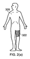
FIG. 1 (a), FIG. 1 (b) and FIG. 1 (c) show a diagram of a set of treatment systems that can be used to treat a cancerous lesion in a patient's arm. FIG. 1 (a) shows an
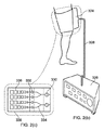
図2(a)、図2(b)および図2(c)は、患者の足の大きな傷を治療するために用いられるシステムの図を示す。図2(a)は、足に大きな開放創322を有する患者320を示す。この傷は、たとえば皮膚病、自動車事故によって、または戦闘もしくは戦争にかかわることによってもたらされ得る。図2(b)は、直流電力供給を搬送する伝送線と制御信号を搬送する伝送線とを含むケーブルアセンブリ328を用いてともに接続された2つのサブシステム324、326を含む治療システム一式を示す。第1のサブシステム326は、直流電源と、制御ユニット(たとえば、マイクロプロセッサおよび/またはデジタル信号プロセッサ)と、適切なユーザインターフェイス(たとえば、モニタを有するキーボード/マウス、キーパッドまたはタッチスクリーンディスプレイを有するLED/LCDディスプレイ)とを有する。第2のサブシステムは、図2(c)により詳細に示されるマイクロ波サブアセンブリ324である。マイクロ波サブアセンブリ324は、マイクロ波供給源発振器330と、マイクロ波電力増幅器332と、電力分割ネットワーク334と、放射アンテナ336とを含む。この実施例では、足(または、類似の構造を有する身体の他の領域)に巻付けることができるように、放射アンテナ336は可撓性基板338上に作製される。マイクロ波電力増幅器332、供給源発振器330、およびマイクロ波サブアセンブリ324に関連する他のマイクロ波電子部品は、望ましくは可撓性アンテナアレイ構造の入力に直接接続されて、挿入損失を最小限にする。
2 (a), 2 (b) and 2 (c) show diagrams of systems used to treat large wounds on a patient's foot. FIG. 2 (a) shows a
この実施例では、複数の進行波アンテナ構造を用いて、可撓性アンテナアレイを形成する。 In this embodiment, a flexible antenna array is formed using a plurality of traveling wave antenna structures.
実際には、足の全周の傷の迅速な治癒に必要な均一な組織効果をシステムがもたらすことができるように、図2(c)に示されるタイプの2つのアンテナアレイがともに用いられてもよい。より大きな表面積を治療すべきである場合には3つ以上のアレイを用いることが望ましいであろう。 In practice, two antenna arrays of the type shown in FIG. 2 (c) are used together so that the system can provide the uniform tissue effect necessary for the rapid healing of wounds around the foot. Also good. If larger surface areas are to be treated, it may be desirable to use more than two arrays.
図3は、皮膚表面24に適用された、この発明の実施例である皮膚治療装置10を示す。装置10は、エネルギ、たとえば予め定められた安定した周波数を有する交流電力をエネルギ源(図示せず)から装置に与えるマイクロ波給電コネクタ12を有する。給電コネ
クタは、任意の好適なタイプ、たとえばSMA、SMB、SMC、MCXまたはSMPなどの同軸接続であってもよい。(たとえば、銅、銀などからなる)接地された導電層14は、給電構造(以下に記載)を介して複数の導電パッチ18に供給される電流のための戻り電流経路を提供するように、誘電体基板16上に取付けられる。各パッチ18は、提供されたマイクロ波エネルギのための放射アンテナの役割を果たすように選択された長方形の形状を有する。放射素子の形状は必ずしも長方形ではない。すなわち、放射素子は、正方形、三角形または円筒形であってもよい。この形状は、電磁場シミュレーションを用いて最適化されてもよい。複数のパッチ18は、規則的な配列で配置され、一緒になって実質的に均一な電磁場を外向きに放出するように基板16の表面上の空隙20によって隔てられている。パッチ18のアレイは、好ましくは生体適合性材料、たとえばパリレンC、テフロン(登録商標)などから形成された誘電体スーパーストレート22によって被覆される。
FIG. 3 shows a
典型的に、スーパーストレート22は、治療中に皮膚24と接触する。しかしながら、より表在性の治療が必要である場合(たとえば、組織のリサーフェシングの場合)には、スーパーストレート22と皮膚24との間に空隙が導入されてもよい。上記空隙と上記組織との間の距離が、信号減衰がたとえば1dB未満であるようなものである場合、アプリケータの表面を組織の表面と直接接触させる必要なく、供給源エネルギの大部分を組織の表面に結合することが可能である。この治療方法の利点は、高温のアプリケータに起因して焼けまたは組織の炭化の点で組織の表面が損傷を受け得る可能性がないはずであること、およびスタンドオフ距離を調整することによって、たとえば装置から突出している1つ以上の誘電体ポスト間に調整可能なねじ式係合を有することによって、エネルギ分布を変更できることである。この方法は、皮膚表面を影響を受けないままにしながら皮膚の表面下の組織に影響を及ぼすために用いることができる。特定の用途は、コラーゲン収縮および毛嚢の房の破壊を含んでいてもよい。
Typically, the
代替的に、放射パッチと皮膚の表面との間で低損失誘電体ブロックが用いられてもよい。エネルギ調整はまた、PINダイオード減衰器を調整して電力レベルを制御することによって、またはPINダイオードスイッチを変調して、送出されたエネルギのパルス幅もしくはデューティサイクルを変更することによってなされてもよい。代替的に、互いに対して放射パッチの位相を制御するためにPINダイオード位相調整器が用いられてもよい。個々のパッチ(または放射素子)に送出された電力レベルの調整と、位相の調整との組合せによって、表面上および表面下の両方の皮膚構造の変化が異なる量のエネルギまたは異なる整合条件を必要とし得るときに、均一なエネルギを大きな表面積にわたる皮膚の表面に送出することができる。したがって、この発明は、治療エリア上の組織構造のばらつきに適合できる、個々に制御可能な放射素子を提供してもよい。 Alternatively, a low loss dielectric block may be used between the radiating patch and the skin surface. Energy adjustment may also be done by adjusting the PIN diode attenuator to control the power level or by modulating the PIN diode switch to change the pulse width or duty cycle of the delivered energy. Alternatively, PIN diode phase adjusters may be used to control the phase of the radiating patches relative to each other. Due to the combination of power level delivered to individual patches (or radiating elements) and phase adjustment, both on-surface and sub-surface skin structure changes require different amounts of energy or different matching conditions. When obtained, uniform energy can be delivered to the surface of the skin over a large surface area. Thus, the present invention may provide individually controllable radiating elements that can adapt to variations in tissue structure on the treatment area.
スーパーストレート22は、取外し可能であり、機器の使い捨て部を形成する。
誘電体基板16は、任意の好適な材料、すなわち、好ましくは治療中の皮膚組織の表面に装置をインピーダンス整合させることを助ける、低いtanδおよび比誘電率を有する誘電材料からなっていてもよい。好適な材料の例は、PTFE、ナイロン、サファイア、およびパリレンCでコーティングされたアルミナ(コーティングの厚みは好ましくは10μm未満である)である。アルミナを用いることの利点は、皮膚構造の比誘電率に匹敵する約10という比誘電率を有すること、および優れた熱伝導率を有することを含む。場合によっては、伝導によって発生する如何なる熱も組織の表面に伝達されることを防ぐために、劣った熱伝導率を有する材料を用いることが望ましいであろう。これは組織の表面の焼けを招く可能性がある。すなわち、熱が皮膚に伝えられるのではなく材料に蓄積される。
The
The
PTFEまたはナイロンの比誘電率は比較的低い傾向があり、たとえば2から4の間で
あり、したがって、誘電体基板層とパッチアンテナ層との間に整合変圧器が必要であり得る。低誘電率誘電体が用いられる場合、誘電体基板層とパッチアンテナ層との間に追加の誘電体層を挟んで、必要なインピーダンス整合を行なうこと、および電力の一部が組織/誘電体界面において反射されるのを防ぐことが好ましい。
The relative permittivity of PTFE or nylon tends to be relatively low, for example between 2 and 4, so a matching transformer may be required between the dielectric substrate layer and the patch antenna layer. When low dielectric constant dielectrics are used, an additional dielectric layer is sandwiched between the dielectric substrate layer and the patch antenna layer to provide the necessary impedance matching and some of the power is at the tissue / dielectric interface It is preferable to prevent reflection.
罹患した皮膚組織を治療しながら皮膚の表面を冷たい状態に保つことが必要である場合には、パッチアンテナアレイはペルティエ冷却器装置上に取付けられることができるであろう。これは、コラーゲン収縮の用途にとって特に興味深いものであり得る。優れた熱伝導率を有するセラミック基板はまた、皮膚の表面から熱を除去することを助け得る。 If it is necessary to keep the skin surface cold while treating the affected skin tissue, the patch antenna array could be mounted on a Peltier cooler device. This can be particularly interesting for collagen contraction applications. A ceramic substrate with excellent thermal conductivity can also help remove heat from the surface of the skin.
マイクロ波エネルギが加えられるときに組織の表面を冷却するために冷却剤またはフリーザ噴霧器で皮膚の表面を噴霧することも可能であり得る。この構成では、マイクロ波エネルギは、マイクロ波エネルギの周波数に関連する深さまで皮膚の層内に吸収され、皮膚の表面は変化しない。冷却剤の送出をマイクロ波パルスの印加と同期させることが好ましいであろう。たとえば、マイクロ波パルスが期間100msを有する場合、パルスよりも50ms前に噴霧器を起動させることが望ましいであろう。
It may also be possible to spray the skin surface with a coolant or a freezer sprayer to cool the tissue surface when microwave energy is applied. In this configuration, microwave energy is absorbed into the skin layer to a depth related to the frequency of the microwave energy and the skin surface does not change. It may be preferable to synchronize the delivery of the coolant with the application of the microwave pulse. For example, if the microwave pulse has a duration of 100 ms, it may be desirable to activate the
図1に示される構造は剛性かつ平坦であるが、でこぼこの組織構造に適合する可撓性アレイを製作するように修正することが可能である。たとえば、ロジャース・コーポレーション(Rogers Corporation)およびシェルダール社(Sheldahl)(現在のマルテック・フレキシブル・サーキッツ社(Multek Flexible Circuits))は、この発明を実施する際に用いられてもよい可撓性のラミネートポリマー回路材料を製造している(たとえば、ロジャース・コーポレーションは、R/flex3600として知られている特定の材料を製作している)。 The structure shown in FIG. 1 is rigid and flat, but can be modified to produce a flexible array that conforms to the bumpy tissue structure. For example, Rogers Corporation and Sheldahl (now Multek Flexible Circuits) are flexible laminates that may be used in the practice of this invention. Manufactures polymer circuit materials (eg, Rogers Corporation makes a specific material known as R / flex 3600).
導電パッチ18が用いられる場合、装置設計はパッチアンテナアレイの理論に基づき、各放射パッチの大きさ(長さ「L」および幅「W」)は有効誘電率の関数として計算され、動作周波数(たとえば、14.5GHz)、パッチアレイを作製するために用いられる材料の誘電率εr、パッチアンテナを用いて治療する皮膚組織の誘電率、および誘電体ブロックまたは空隙(用いられる場合)の誘電率に依存する。スーパーストレート22はまた、アンテナ構造全体の性能に影響を及ぼすことになり、これはパッチアンテナアレイを設計および最適化する際に考慮に入れなければならない。スーパーストレート材料の厚みが小さい、たとえば5〜10μmである場合、影響は無視できるほどのものであり得て、無視することができる。非常に薄い層のみが用いられる場合には、比較的損失の大きい、すなわち0.001より大きなtanδを有する材料を用いることも可能である。
If
厚いスーパーストレート22に起因する有効誘電率の変化は実質的な変化をもたらす可能性があり、変化の量は、スーパーストレート22の厚みおよび比誘電率によって支配される。
The change in effective dielectric constant due to the
表2は、アプリケータを皮膚の表面に接触させた状態での乾燥した皮膚と湿った皮膚に関連する誘電負荷についてcm2当たりのパッチの数を確認するために行なわれた理想的な計算に基づく情報を示している。これらの数字は、放射パッチが皮膚と直接接触しており、放射パッチが作製される基板材料がパッチの大きさに影響を与えないと仮定している。また、材料損失に起因する誘電率の成分が比誘電率と比較して低いと仮定している。より正確な数字を得るためおよび/または上で無視した要因を考慮に入れるために、電磁場シミュレーションを行なうことができ、パッチアレイまたはこの発明とともに用いるのに適した他のアンテナ構造の大きさの最適化を行なうことが可能である。 Table 2 shows the ideal calculations performed to ascertain the number of patches per cm 2 for the dielectric load associated with dry and wet skin with the applicator in contact with the surface of the skin. Based on the information. These numbers assume that the radiating patch is in direct contact with the skin and the substrate material from which the radiating patch is made does not affect the size of the patch. Further, it is assumed that the component of dielectric constant due to material loss is lower than the relative dielectric constant. In order to obtain more accurate numbers and / or to take into account the factors neglected above, electromagnetic field simulations can be performed, optimizing the size of the patch array or other antenna structure suitable for use with the present invention Can be performed.
上記の周波数で動作するソリッドステートトランジスタ装置は、トライクイント・セミコンダクター社(TriQuint Semiconductor)、東芝セミコンダクター社、ヒッタイト・マイクロウェーブ・コンポーネンツ社(Hittite Microwave Components)、および三菱セミコンダクター社から商業的に調達可能である。14.5GHzで動作する装置は十分に確立しつつあるのに対して、31GHz、45GHz、60GHz、77GHz、および94GHzで動作する装置は現在利用可能になり始めている。トライクイント・セミコンダクター社は、現在、45GHzおよび31GHzで動作する4W装置を製造している。この電力出力では、いくつかの放射素子を給電するために単一の装置が用いられてもよい。半導体技術、特にPHEMT装置の近年の進歩により、100GHzまでの周波数で発生する100mWから2Wの電力レベルが提供される。 Solid state transistor devices operating at the above frequencies are commercially available from TriQuint Semiconductor, Toshiba Semiconductor, Hittite Microwave Components, and Mitsubishi Semiconductor. is there. While devices operating at 14.5 GHz are becoming well established, devices operating at 31 GHz, 45 GHz, 60 GHz, 77 GHz, and 94 GHz are now becoming available. Triquint Semiconductor currently manufactures 4W devices that operate at 45 GHz and 31 GHz. At this power output, a single device may be used to power several radiating elements. Recent advances in semiconductor technology, particularly PHEMT devices, provide power levels from 100 mW to 2 W that occur at frequencies up to 100 GHz.
表2中の数字は、全部の半波長負荷パッチを表面積10mm2の正方形に収容できるように、端数を切上げるまたは切下げている。実際の実施の際には、利用可能な基板材料のエリア上に作製できるパッチの数を最適化するために大きさをわずかに拡張または縮小してもよく、電磁場モデリングから得られた結果に従って大きさは変化し得る。たとえば、寸法が10.62mm(W)×10.62mm(L)に増大される場合、動作周波数が14.5GHzであれば16個全部の半波長パッチをアレイにおいて用いることができるであろう。これらの寸法は、シミュレーションが行なわれると変化する。なぜなら、損失の大きい生物組織構造とアンテナ構造との間の相互作用が考慮に入れられるためである。最も単純なレベルで、構造全体に関連する誘電率の3つの値がある。3つの値とは、生物組織(皮膚)の複素誘電率、スーパーストレート層の複素誘電率、および基板層の複素誘電率である。治療エリアを増大させるために均一な態様でパッチの数を増やすことが可能であり、たとえば31GHzでは、表面積が4cm2である正方形の治療アプリケータを作製するために144個のパッチを用いることができ、したがって、表面積が16cm2である正方形の治療アプリケータを作製するには576個のパッチが必要になるであろう。 The numbers in Table 2 are rounded up or down to accommodate all half-wave load patches in a square with a surface area of 10 mm 2 . In actual implementation, the size may be slightly expanded or reduced to optimize the number of patches that can be made on the area of available substrate material, and increased according to the results obtained from electromagnetic field modeling. It can change. For example, if the dimensions are increased to 10.62 mm (W) x 10.62 mm (L), then all 16 half-wave patches could be used in the array if the operating frequency is 14.5 GHz. These dimensions change as the simulation is performed. This is because the interaction between the lossy biological tissue structure and the antenna structure is taken into account. At the simplest level, there are three values of dielectric constant associated with the entire structure. The three values are the complex dielectric constant of the biological tissue (skin), the complex dielectric constant of the superstrate layer, and the complex dielectric constant of the substrate layer. The number of patches can be increased in a uniform manner to increase the treatment area, eg at 31 GHz, 144 patches can be used to create a square treatment applicator with a surface area of 4 cm 2. Could thus require 576 patches to make a square treatment applicator with a surface area of 16 cm 2 .
図4は、この発明の実施例に従う治療機器一式100に含まれる構成要素の図を示す。図5は、その機器の概略図を示し、ここでは、マイクロ波エネルギ源、給電構造および放射アンテナアレイのために用いられる機器構成要素はすべて、単一の基板上に集積され、それによって、コンパクトな全体設計を作り出している。垂直積層技術を用いて、機器100は複数の層からなっている。バッテリまたは交流/直流コンバータ(すなわち、電源)102は、ユーザによって操作可能な制御およびディスプレイ装置を含む第1の層104上に取付けられる。第1の層104は、機器を制御するためのプロセッサを含む第2の層106上に取付けられる。この層はまた、故障状態を監視し、第1のプロセッサが動作不良を起こした場合に保護手段の役割を果たすように用いられる「ウォッチドッグ」として知られている第2のプロセッサを含んでいてもよい。第2の層106は、マイクロ波信
号生成ラインアップを含む第3の層108上に取付けられる。第3の層108は、生成されたマイクロ波信号を昇圧するためのマイクロ波増幅器ラインアップ(たとえば、複数のMMICまたはMHEMT装置)を含む第4の層110上に取付けられる。第4の層110は、第5の層112上に取付けられ、第5の層112は、生成されたマイクロ波信号を分けかつエネルギを放射素子に伝送するように配置されたパワースプリッタのネットワークを組入れる(たとえば、マイクロストリップトラックの)給電構造を含む。第5の層112は、第6の層113上に取付けられ、第6の層113は、アンテナ構造の放射素子に与えられる前に、分けられた信号を昇圧するための電力増幅器(たとえば、MMIC装置)のアレイを含む。第6の層113は、第7の層114上に取付けられ、第7の層114は、各放射素子に送出された電力および各放射素子から反射された電力を監視するように、および、たとえば治療すべき組織とのインピーダンス整合を確実にするために各信号を調整するように配置された信号制御装置のアレイを含む。第7の層114は、第8の層116上に取付けられ、第8の層116は、各々が信号制御装置のアレイから、分けられた信号を受信する放射素子(たとえば、導電パッチ、スロットライン、または共平面導波路サスペンド型パッチアンテナ)のアレイ(たとえば、規則的なパターン)を含む。第8の層は、図4に示される構成に類似した放射構成を提供するために、放射素子とは反対側の面上に、接地された導電性コーティングを有していてもよい。生体適合性の取外し可能な(使い捨ての)第9の層117が第8の層116上に設けられる。第9の層117は、使用中、治療すべき組織と接触する(すなわち、それは上述のスーパーストレート層である)。
FIG. 4 shows a diagram of the components included in a
したがって、機器一式が層のサンドイッチ構造内に含まれることができる。パワーデバイスを放射パッチ上に直接取付けることの主な利点は、伝送損失(または、給電線損失もしくは挿入損失)を最小限にすることである。これは、高周波数(たとえば、24GHz、31GHz、45GHz、60GHz、77GHz、94GHz、およびそれを上回る周波数)での動作にとって特に興味深いものである。図1および図2に示されるように治療システム全体を2つの別個のブロックに分割することが望ましいであろう。第1のブロックは、スーパーストレート層、アンテナアレイ、給電構造、発電装置、および供給源発振器からなるマイクロ波サブアセンブリを含んでいてもよい。第2のブロックは、直流電源、制御電子機器(マイクロプロセッサおよび/またはDSPおよび/またはウォッチドッグ)、およびユーザインターフェイスを含んでいてもよい。 Thus, a complete set of equipment can be included in a layered sandwich structure. The main advantage of mounting the power device directly on the radiating patch is to minimize transmission loss (or feeder loss or insertion loss). This is particularly interesting for operation at high frequencies (eg, frequencies of 24 GHz, 31 GHz, 45 GHz, 60 GHz, 77 GHz, 94 GHz and above). It may be desirable to divide the entire treatment system into two separate blocks as shown in FIGS. The first block may include a microwave subassembly comprising a superstrate layer, an antenna array, a feed structure, a power generator, and a source oscillator. The second block may include a DC power source, control electronics (microprocessor and / or DSP and / or watchdog), and user interface.
各層における構成要素が図4に示されている。マイクロ波信号は安定周波数源126によって生成され、安定周波数源126は、電磁スペクトルの超高周波数(SHF)または極高周波数(EHF)領域内に含まれる単一周波数で、より詳細には、14.5GHz、24GHz、31GHz、45GHz、66GHz、77GHz、または94GHzで(周波数変動は数百kHzに限定される)信号を提供する。ここに示される安定周波数源126は、マイクロ波供給源126の周波数安定性を導き出す基準信号を含む位相ロック誘電体共振器発振器(dielectric resonator oscillator)(DRO)の形態を取り、上記基準信号の供給源(図示せず)は、1MHzから100MHzの間であるが、より好ましくは10MHzから50MHzの間の範囲内の周波数で動作する温度安定水晶発振器を備えていてもよい。電圧制御発振器(voltage controlled oscillator)(VCO)またはガンダイオード発振器などの他の周波数源が用いられてもよいが、この発明ではDROを用いることが好ましい。システムの周波数安定性を高めるために、2つの基準発振器をマイクロ波供給源126内で用いることができる。複数の安定周波数源を用いて、複数のマイクロ波周波数源を用いることができるようにして、単一のパッチアンテナアレイを励起することが好ましいであろう。この構成では、安定周波数源は周波数合成器の形態を取ってもよい。
The components in each layer are shown in FIG. The microwave signal is generated by a
安定周波数源126は、3dB 0°パワースプリッタ128の入力ポートに接続され
る。スプリッタ128の目的は、位相変化を導入することなく、供給源126が生成した電力を2つの等しい割合に分けることである。
The
スプリッタ128からの第1の出力は第1の信号アイソレータ132の入力に接続され、スプリッタ128からの第2の出力は減衰パッド130の入力に接続される。減衰器パッド130の出力はマイクロプロセッサ124への入力であり、マイクロプロセッサ124では、信号を用いて周波数源126の状態を監視する。減衰器パッド130の目的は、マイクロプロセッサ124への入力に入射する信号レベルを限定することである。信号供給源126が不適切に機能していることを信号が示す場合、マイクロプロセッサ124は、エラーが発生したことを合図し、システムは適切な動作を行なう。すなわち、エラーメッセージが生成され、および/またはシステムが停止される。
A first output from
第1の信号アイソレータ132の目的は、たとえばロードプリング、または信号供給源126が生成した信号に影響を及ぼし得る別の条件に起因して供給源126において周波数変化を引起す第1の変調ブレークスルー阻止フィルタ134の入力に存在する如何なる不整合信号も防ぐことである。実際には、フィルタ134の入力ポートが十分に整合されていればアイソレータ132は必要ないかもしれないが、アイソレータ132は予防措置として含まれている。第1の変調ブレークスルーフィルタ134の出力は変調スイッチ136の入力に接続され、変調スイッチ136の機能は、安定周波数源126が生成した信号を変調して、システムがパルスモードで動作できるようにすることであり、それによって、ユーザ制御およびディスプレイユニット118ならびにマイクロプロセッサ124を用いて、デューティサイクル、パルス幅、および(望まれる場合)パルス形状を修正できる。第1の変調ブレークスルーフィルタ134の目的は、変調スイッチ136が生成した高速スイッチング信号内に含まれる周波数成分が安定周波数源126に戻り、その出力信号に影響を及ぼすのを防ぐことである。
The purpose of the
変調スイッチ136への入力制御信号135はマイクロプロセッサ124から生じる。この制御信号135はトランジスタ−トランジスタ論理(transistor-transistor logic)(TTL)レベル信号であってもよく、他の信号フォーマット(たとえば、エミッタ結合論理(emitter coupled logic)(ECL))が可能である。
The
変調スイッチ136からの出力は、第2の変調ブレークスルー阻止フィルタ138の入力に接続され、第2の変調ブレークスルー阻止フィルタ138の機能は、特定の治療法のために変調スイッチ136が生成し得る高速スイッチング信号内に含まれる周波数成分が、後続の前置増幅器144および電力増幅器146に入り、たとえば信号の歪み、誤った出力電力レベル、またはたとえば出力電力段発振の顕在化によるこれらのユニットに対する損傷、または信号の過励振を引起すのを防ぐことであり、信号の過励振は、周波数源126が生成する信号もしくは増幅器144、146の帯域幅内である、すなわち上記増幅器が利得を与える信号の周波数と同じ周波数で生じるスイッチング信号内に含まれる高調波のうちの1つによって引起される。
The output from the
ブレークスルー阻止フィルタの実際の実施は単に長方形導波路セクションであってもよく、そこでは、導波路セクションの遮断周波数よりも低い周波数は阻止され、したがって、導波路セクションはハイパスフィルタの役割を果たす。 The actual implementation of the breakthrough blocking filter may simply be a rectangular waveguide section, where frequencies below the cutoff frequency of the waveguide section are blocked, thus the waveguide section acts as a high pass filter.
第2の変調ブレークスルー阻止フィルタ138からの出力は、第2の信号アイソレータ140の入力に接続される。上記第2のアイソレータ140からの出力は可変信号減衰器142に接続され、可変信号減衰器142の機能は、マイクロプロセッサ124が生成した入力制御信号143を用いて信号減衰のレベルを変化させることによってシステム電力レベルを制御できるようにすることである。可変信号減衰器142は、アナログ減衰器で
ある場合もあれば、デジタル減衰器である場合もあり、反射型である場合もあれば、吸収型である場合もある。この減衰器は、いくつかのパルス形状またはシーケンスを生成するようにマイクロプロセッサ124によって制御されてもよい。第2の信号アイソレータ140の機能は、可変減衰器142の入力ポートと第2の変調ブレークスルー阻止フィルタ138の出力ポートとを分離することである。第2の信号アイソレータ140は、優れた設計実践のために挿入されており、劣化またはマイクロ波サブアセンブリに対する損傷を引起すことなく機器から割愛することができる。
The output from the second modulation breakthrough blocking filter 138 is connected to the input of the second signal isolator 140. The output from the second isolator 140 is connected to a
可変減衰器142からの出力は信号前置増幅器144の入力に接続され、信号前置増幅器144の機能は、後続の電力増幅器段146への入力の駆動にとって許容できるレベルに信号を増幅することである。前置増幅器144は、電力増幅器段146を駆動するために必要な10dBから40dBの間の利得を与えてもよい。前置増幅器144は、単一の小型マイクロ波集積回路(miniature microwave integrated circuit)(MMIC)、複数のMMIC、MMICと単品部品との組合せ、または複数の単品部品の形態のものがあってもよい。MMIC装置は単品部品にとって好ましい。なぜなら、これらの装置は通常、より多くの利得を生み出すためであり、したがって、単品部品のカスケード接続の代わりに単一のMMICを用いてもよい。これは、空間(大きさ)の最小化および熱の放散の点で有利である。たとえば、トライクイント社の半導体装置TGA8658−EPU−SGを用いることができる。前置増幅器において用いられる好ましい装置技術はガリウム砒素(GaAs)技術であるが、実現性のある代替案を提供し得る他の台頭しつつある技術、たとえば窒化ガリウム(GaN)または高電子移動度トランジスタ(HEMT)がある。
The output from the
前置増幅器144からの出力は入力を電力増幅器146に供給し、電力増幅器146の機能は、治療装置の放射アンテナ構造を供給するために必要なレベルに信号を昇圧することである。
The output from the
電力増幅器146からの出力は、3dBパワースプリッタ148のネットワークに供給される。パワースプリッタ148は、機器のそれぞれの層112上にマイクロストリップ構造として作製されることができる。図6に示されるように、電力分割ネットワークは、電力増幅器からの信号を16個の給電装置A1〜A16に分ける15個のパワースプリッタSP1〜SP15を備え、16個の給電装置A1〜A16の各々は、次の層113におけるそれぞれの増幅器150に接続される。したがって、この実施例では、増幅器ネットワークは単一の供給源から給電される。
The output from the
16個の増幅器150の各々は、その出力が導電放射パッチまたはアンテナ154を駆動するように配置される。16個の増幅器150は、この目的で駆動信号S1〜S16を生成する。増幅器150は各々、33dBm(2W)の1dB圧縮点において電力を生成し、16dBの利得を有し、41GHzから46GHzの間の周波数範囲で動作することができる。好適な装置として、トライクイント社の半導体装置TGA4046−EPUがある。
Each of the 16
信号S1〜S16は、隣接するパッチが互いに直交して放射を放出するように8つの層116上の導電放射パッチ154に供給される。
Signals S 1 -S 16 are provided to
治療中の組織の領域のインピーダンスのばらつきを調整するように電磁場全体が集束(操縦)され得るように、放射パッチの各々に供給されたマイクロ波電力を独立して制御することが望ましいであろう。この独立した制御は、第5の層114に取付けられた信号制御装置152によって行なわれる。図7に示されるように、各信号制御装置は、フロント順方向方向性結合器156と、移相器(たとえば、PINダイオードまたはバラクタダイ
オード)158と、順方向電力方向性結合器160と、反射電力方向性結合器162とを備える。結合器156、160、162は、装置を通って順方向に進むか、または信号が組織から反射されて供給源の方に戻る反対方向に進む電力を検出するように配置される。信号は、位相および/または大きさ検出器回路155を介してマイクロプロセッサ124に供給される。検出器は、位相および大きさの両方の情報を測定することが望ましいヘテロダイン受信機の形態を取る場合もあれば、大きさ情報のみを必要とするホモダイン受信機の形態を取る場合もある。大きさ情報を検出および処理することのみが必要である単純なダイオード検出器も用いてもよい。これらの信号に基づいて、マイクロプロセッサ(および/またはDSP)は、生じ得る如何なるインピーダンス不整合も計算でき、必要な制御信号を移相器158に送ることによってインピーダンス不整合を調整できる。
It would be desirable to independently control the microwave power supplied to each of the radiating patches so that the entire electromagnetic field can be focused (steered) to adjust for impedance variations in the area of tissue being treated. . This independent control is performed by a
換言すれば、方向性結合器156、160、162および(たとえば、ヘテロダイン、ホモダイン、もしくはダイオードタイプの)マイクロ波検出器または受信機は、順方向電力信号および反射電力信号の位相および/または大きさを測定する。次いで、これらの信号を用いて、移相器158によってエネルギ送出プロファイルを制御する。移相器(たとえば、PINまたはバラクタダイオード)が信号の位相のみを変更している間、大きさおよび位相の両方を変更し得る整合フィルタを用いることができる。
In other words,
図6は、図5の積重ねられた第5の層112、積重ねられた第6の層113、積重ねられた第7の層114、および積重ねられた第8の層116の図をそれぞれ示し、それらの層上の構成要素間の給電接続を示す。実際には、隣接する層の構成要素は互いの上にあり、明確にするために、図6はそれらの層を同心の構成で示している。
FIG. 6 shows views of the stacked
図6に示される構成は、16個の導電パッチに分割されるマイクロ波エネルギ源のためのものである。元のマイクロ波エネルギ源を16個の別個の供給源または信号に分割するために、第5の層112には15個の1対2パワースプリッタ148(SP1〜SP15)がカスケード接続アレイで取付けられている。したがって、元の供給源は1つの第1の生成スプリッタSP1によって2つに分割され、結果として生じる2つの供給源の各々はさらに第2の生成スプリッタSP2、SP3によって2つに分割され、結果として生じるそれら4つの供給源の各々はさらに第3の生成スプリッタSP4〜SP7によって2つに分割され、最終的に、結果として生じるそれら8つの供給源の各々はさらに第4の生成スプリッタSP8〜SP15によって2つに分割される。第4の生成スプリッタSP8〜SP15からの各出力は、第6の層113における16個の増幅器150(Amp1〜Amp16)のうちのそれぞれ1つに供給される。次いで、増幅器出力は、第7の層114におけるそれぞれの信号制御装置152(C1〜C16)を介して、第8の層116におけるそれぞれの放射パッチ154(P1〜P16)に供給される。パッチ154は正方形であり、これは、放出される電磁場がほとんど2つの対向する端縁から生じることを意味している。図6では、放射端縁155は太い線によって示されているのに対して、非放射端縁153は細い線によって示されている。給電線は、隣接するパッチの放射端縁155が確実に互いに直交するようにパッチ154に接続される。これは、放射アンテナアレイのエリアにわたってもたらされる電磁場の均一性を最大にすることができ、ひいては、アンテナアレイのエリアにわたって均一な組織効果をもたらすことができる可能性を最大にする。
The configuration shown in FIG. 6 is for a microwave energy source that is divided into 16 conductive patches. To divide the original microwave energy source into 16 separate sources or signals, the
実際には、図6に示される構造では給電線損失を考慮に入れる必要があり得る。特に、装置を通る好適な信号レベルを維持するために緩衝またはブースタ増幅器を含める必要があり得る。各パワースプリッタ148は典型的に、それに関連する3dBの損失を有する。45GHzでは、7dBまでの構成要素間の給電線損失が起こり得て、これは、パワースプリッタカスケード接続の各経路(マイクロストリップ線)に沿って10dBまでの全体損失に繋がるであろう。この損失は、パワースプリッタごとの前または1つおきのパワースプリッタの前に緩衝増幅器を置くことによって補償されることができる。実際の構成
は、装置について計算された電力収支に依存する。電力収支の一例について、以下の図20に関連して説明する。
In practice, the structure shown in FIG. 6 may need to take feeder line losses into account. In particular, it may be necessary to include a buffer or booster amplifier to maintain a suitable signal level through the device. Each
この発明の1つの重要な特徴は、エネルギ源から放射素子に電力を伝達する手段である。パッチアレイ内に含まれる各パッチアンテナにはマイクロ波エネルギを供給する必要がある。一般的に言って、並列給電および直列給電の2つの主な給電構造がある。 One important feature of the present invention is the means of transferring power from the energy source to the radiating element. It is necessary to supply microwave energy to each patch antenna included in the patch array. Generally speaking, there are two main feeding structures: parallel feeding and series feeding.
並列給電は単一の入力ポートを有し、多数の給電線が並列に接続されて、出力ポートを構成する。給電線の各々は、個々の放射素子(またはパッチ)で終端する。 The parallel power supply has a single input port, and a large number of power supply lines are connected in parallel to form an output port. Each feed line is terminated with an individual radiating element (or patch).
直列給電は、近接結合、直接結合、プローブ結合、またはアパーチャ結合を含むさまざまな手段によって線に沿って配された個々の素子にエネルギのごく一部を累進的に結合する連続した伝送線からなる。直列給電は、給電線が整合負荷で終端する場合には進行波アレイを構成し、給電線が開回路または短絡で終端する場合には共振アレイを構成する。 A series feed consists of a continuous transmission line that progressively couples a small portion of energy to individual elements placed along the line by various means including proximity coupling, direct coupling, probe coupling, or aperture coupling. . The series feed forms a traveling wave array when the feed line is terminated with a matching load, and a resonant array when the feed line is terminated with an open circuit or a short circuit.
直列給電の一例は、放射伝送線または「漏洩フィーダ」であり、放射素子の組で進行波を搬送する伝送線からなっていてもよい。各素子は、総電力のうちのほんのわずかの部分を放射するであろう。そして線に沿って累進的に各素子の大きさを調整することによって、長さに対する、均一に近い電力強度が達成可能であろう。この場合、従来の非近距離場アンテナに必要であるように素子は同相ではないが、これはこの用途では重要でないはずである。この構成では、各放射素子のインピーダンスは伝送線の特性インピーダンスよりも低くしなければならず、たとえば、伝送線給電インピーダンスが50Ωであるときには放射素子のインピーダンスは12.5Ωであってもよく、そうでなければ放射パッチの第1の対によって放射される電力が過剰になり、入力における反射減衰量は劣ったものになる(不整合状態)。放射構造に沿って均一な電力を維持するために放射パッチの大きさを変えることが好ましいであろう。パッチアンテナアレイを構築するために用いることができるであろう可能な材料は、シェルダール社製のノバクラッド(NovaClad)、タコニック社(Taconic)製の薄い銅覆PTFE/ガラス、またはロジャース・コーポレーション社製のR/Flex液晶ポリマー回路材料である。 An example of a series feed is a radiating transmission line or “leakage feeder”, which may consist of a transmission line that carries traveling waves with a set of radiating elements. Each element will radiate only a small portion of the total power. And by adjusting the size of each element progressively along the line, a near uniform power intensity for the length could be achieved. In this case, the elements are not in phase as is necessary for a conventional non-near field antenna, but this should not be important for this application. In this configuration, the impedance of each radiating element must be lower than the characteristic impedance of the transmission line. For example, when the transmission line feeding impedance is 50Ω, the impedance of the radiating element may be 12.5Ω. Otherwise, the power radiated by the first pair of radiating patches will be excessive and the return loss at the input will be poor (mismatched state). It may be preferable to change the size of the radiating patch in order to maintain uniform power along the radiating structure. Possible materials that could be used to construct a patch antenna array are Sheldal NovaClad, Taconic thin copper clad PTFE / glass, or Rogers Corporation R / Flex liquid crystal polymer circuit material.
並列給電も直列給電も、放射素子を有する共平面導波路としてまたは別個の伝送線層において実現されることができる。パッチと同じ平面に置かれた給電線は放射し、放射パッチが放出する放射と干渉する可能性がある。これは、給電線が制御された伝送線であり、放射が放射パッチから強制的に行なわれる場合には、問題ではないかもしれない。この問題はまた、給電線の上方に放射パッチを吊り下げることによって克服され得る。たとえば、共平面導波路給電サスペンド型パッチアンテナアレイが作製されてもよい。 Both parallel and series feeds can be realized as coplanar waveguides with radiating elements or in separate transmission line layers. Feedlines placed in the same plane as the patch will radiate and may interfere with the radiation emitted by the radiating patch. This may not be a problem if the feed line is a controlled transmission line and radiation is forced from the radiating patch. This problem can also be overcome by suspending the radiating patch above the feeder line. For example, a coplanar waveguide fed suspend type patch antenna array may be fabricated.
パッチアレイ用の給電構造を設計する際、(典型的には動作周波数の関数である)導体および誘電体損失、ならびに湾曲部、接合部および遷移部などの不連続部に起因するスプリアス放射も考慮すべきである。これらの損失は、給電装置の挿入損失全体を構成し、各放射パッチに送出され得る最大可能電力を検討する際の重要な決定要因である。これらの給電構造の設計において、給電線の劣化を最小限にするために、たとえば200Ωの実現可能な高特性インピーダンス給電線が用いられてもよい。挿入損失または給電線損失および最適化の複雑さを低減するために、分周器段の数を最小限に抑えるべきである。 When designing feed structures for patch arrays, take into account conductor and dielectric losses (typically a function of operating frequency) and spurious emissions due to discontinuities such as bends, junctions and transitions Should. These losses constitute the overall insertion loss of the feeder and are an important determinant in considering the maximum possible power that can be delivered to each radiating patch. In the design of these feed structures, in order to minimize the degradation of the feed line, a high characteristic impedance feed line that can be realized, for example, 200Ω may be used. In order to reduce insertion loss or feeder loss and optimization complexity, the number of divider stages should be minimized.
図8および図9(a)、図9(b)および図9(c)は、スロット付きアンテナ構成に基づく皮膚治療装置を示す。図8では、給電線に沿ってスロットの幅が広くなっている。これは、同じ量のマイクロ波エネルギが各スロットから放出されることを確実にする定評のある方法であり、皮下治療または皮膚の若返りもしくはリサーフェシングのための実現性のある用途を提供する。この構造は、接地面に形成された(たとえば、切込まれた)ス
ロットのアレイを備える。基板層上にマイクロストリップ線が作製され、それによって、線(図8では図示せず)がスロットを横断する。この構造の利点は、基板の上に給電線を作製することが比較的容易であることである。スロットの大きさ(長さ)とマイクロ波エネルギ給電装置(供給源)からスロットまでの距離との間の関係が通常線形ではないので、スロットの間隔およびスロットの大きさの点で構造を最適化するために電磁場シミュレーションツールが用いられる。伝送線の端部付近での電力低減を考慮に入れるために、理論的には見られる遠位スロット(供給源から最も遠く離れたスロット)の長さを長くする必要があることがわかった。反復的な態様で構成を最適化するために経験的実験も用いてもよい。
8 and 9 (a), 9 (b) and 9 (c) show a skin treatment device based on a slotted antenna configuration. In FIG. 8, the width of the slot is increased along the feeder line. This is a well-established method to ensure that the same amount of microwave energy is released from each slot, providing a feasible application for subcutaneous treatment or skin rejuvenation or resurfacing. This structure comprises an array of slots (eg, cut) formed in the ground plane. A microstrip line is created on the substrate layer, whereby a line (not shown in FIG. 8) traverses the slot. The advantage of this structure is that it is relatively easy to make a feed line on the substrate. Since the relationship between the slot size (length) and the distance from the microwave energy feeder (source) to the slot is usually not linear, the structure is optimized in terms of slot spacing and slot size In order to do this, an electromagnetic field simulation tool is used. It has been found that in order to take into account the power reduction near the end of the transmission line, it is necessary to increase the length of the distal slot (the slot farthest from the source) seen in theory. Empirical experiments may also be used to optimize the configuration in an iterative manner.
図8における装置200は、供給源発振器202を含み、供給源発振器202は、本明細書に記載する離散周波数、たとえば14.5GHz、24GHz、31GHz、45GHz、60GHz、77GHz、または94GHzのうちのいずれかまたはいくつかで動作するVCO、DRO、ガンダイオード、SAW装置、または周波数合成器のうちのいずれかであり得る。供給源発振器202からの出力は、増幅器ラインアップを含む給電構造を介して、8つのスロット付きアンテナ215のアレイに供給される。供給源発振器202からの出力は、第1に、一次および二次3dBスプリッタ206、208によって4つの信号に分けられる前に、一次増幅器204によって増幅される。これらの信号の各々は、三次3dBスプリッタ212によって2つに分けられる前に、二次増幅器210によって増幅される。結果として生じる8つの信号の各々は、それぞれのスロット付きアンテナ215に供給される前に、三次増幅器214によって再び増幅される。
The
図8に示されるように、各アンテナ215は、中にスロット218が形成された接地された導電層216を有する。各スロットから放出されたエネルギが同じであるように、およびスロットの集合からの電磁場が均一であるように、スロット218の幅はアンテナ215の長さに沿って広くなっている。スロットの寸法は、電磁場シミュレーションを用いることによって決定されてもよい。
As shown in FIG. 8, each
スロット付きアンテナの構造は、図9(a)、図9(b)および図9(c)に示される代替的な構成を参照してさらに理解でき、図9(a)、図9(b)および図9(c)では、代替的なスロット付きアンテナ構造220のさまざまな図が与えられている。図9(a)は、複数のマイクロストリップ給電線222が誘電体基板224上に作製された上面図を示す。各線には、上述のように、増幅器ラインアップからマイクロ波電力信号が供給される。
The structure of the slotted antenna can be further understood with reference to the alternative configurations shown in FIGS. 9 (a), 9 (b), and 9 (c), and FIGS. 9 (a), 9 (b). And in FIG. 9 (c), various views of an alternative slotted
図9(b)は、装置の底部(皮膚に面する)面を示す。ここでは、接地された導電層226は誘電体基板224上に作製される。(便宜上等しい幅を有するように示される)スロット228が、接地された導電層226および誘電体基板層224に形成されて、マイクロストリップ給電線222の一部を露出させる。この構造は、スロット228が放射素子の役割を果たすように設計される。スロットの大きさは、動作周波数での放射の波長に応じて選択される。実際の値は、電磁場シミュレーションから得られてもよい。誘電体基板224の厚みは、1波長よりもはるかに少ないように選択される。図9(c)は、アンテナ220の側面図を示す。
FIG. 9 (b) shows the bottom (skin facing) surface of the device. Here, the grounded
マイクロストリップ線222は好ましくは、最大E場または最大H場をスロットを通して組織に放射できるように設置される。したがって、スロットの長さは波長の約半分である。高いマイクロ波周波数(たとえば、31GHz、45GHz、60GHz、77GHz、または94GHz)が用いられる場合、スロットは互いに近接して位置決めされることができ、したがって、マイクロ波放射による浸透深さが限定された状態で、アプリケータの表面全体にわたって均一なエネルギを発生させるための必要な条件を提供する。
The
図10は、この発明において用いることができる給電構造の具体的な例を示し、直列に接続された複数の放射パッチ37を給電するために共同の(並列な)給電装置35が用いられてもよい。この構成について以下で詳細に説明する。非常に大きなアレイの場合、放射素子の各々まで走っている給電線の長さはひどく長い場合があり、その結果、挿入損失が許容できないほどに高くなる。たとえば、45GHzでは、ほんの数センチメートルの長さで挿入損失が数dBになり得る可能性がある。有効な対称的な共同給電アレイを設計する際に、以下のステップを取らなければならない。
FIG. 10 shows a specific example of a feeding structure that can be used in the present invention, and even when a joint (parallel) feeding
1) 結合構造の適切な寸法決めを通じてまたは4分の1波変圧器を用いることによって、放射パッチを確実に給電線に整合させる。 1) Ensure that the radiating patch is matched to the feed line through proper sizing of the coupling structure or by using a quarter wave transformer.
2) 必要であれば4分の1波変圧器によって入力線に整合されるT−接合に、隣接する素子からの給電線の各対を確実に接続させる。 2) Ensure that each pair of feeders from adjacent elements is connected to a T-junction matched to the input line by a quarter wave transformer if necessary.
3) 給電線をアレイの給電ポイントに接続する最後の段階に到達するまで繰返す。
図10に示される共同給電構成では、放射パッチ18は、端縁において200Ωの入力インピーダンスを有し、特性インピーダンスが200Ωである給電線45に接続される。隣接する素子からの給電線45は、T−接合を用いて接合され、140Ωの4分の1波変圧器44を用いて、(特性インピーダンスが200Ωである)単一の供給線43に戻るように変圧される。対象の周波数で波長の4分の1の奇数倍に対応する長さを有する(すなわち、その長さは(2n−1)λL/4であり、ここで、λLは負荷波長であり、nは整数である)変圧器も、線が損失のないものであると仮定すると、同じ変圧を行なうことになる。短波長では、4分の1波長よりも大きな長さを有する、すなわち4分の1波長の奇数倍に等しい長さを有する線を用いることが実際には必要であるかもしれない。伝送線が確実にインピーダンス変圧器の役割を果たすようにするために、誘電材料の特性は安定していなければならない。λ/4よりも長い、すなわち3/4λまたは5/4λなどの変圧器が用いられる場合、この特徴は特に重要である。なぜなら、所望の4分の1電気波長は、そうでなければ、望ましくない電気的長さに修正されるためであり、たとえば、最悪の場合には、それは電気的波長の2分の1の倍数になる可能性があり、変圧を全く行なわない可能性がある。次のステップにおいて、供給線の隣接する対は次いで別のT−接合において接合され、そこでは、140Ωの4分の1波変圧器42によって、さらなる単一の供給線41(特性インピーダンスは200Ωである)に戻るように同様に変圧される。このプロセスは、さらなる供給線41の対が最後のT−接合において接合されるように繰返される。最終の変圧は、71Ωの4分の1波変圧器40を用いて、2つの200Ω線の並列の組合せ(すなわち、100Ω)を、アレイ全体を給電するために用いられるエネルギ源38からの入力線39(特性インピーダンス=50Ω)と整合させる。インピーダンス整合は、式、すなわちZtrans=√(ZinZout)を用いて計算され、今回の場合、最後の接合では√(50×100)=71Ωに対応する。
3) Repeat until reaching the final stage of connecting the feed line to the feed point of the array.
In the joint feeding configuration shown in FIG. 10, the radiating
図11および図12は、この発明において用いることができる給電構造の別の具体的な例を示す。ここで、(治療ゾーンの大きさに応じて、8、16、32、64、128などの番号が付けられている)パッチのアレイは、各パッチが単一のMMIC増幅器によって給電されるように配置される。図11は、この構成の斜視図を示し、図11では、複数の電力増幅器48が装置の上層52上に取付けられている。複数の電力増幅器48は、安定周波数エネルギ源(図示せず)から入力信号50を受信するように配置される。それらの出力信号は、たとえば低損失伝送線を用いて同軸コネクタ54(たとえば、SMAコネクタ)に供給され、同軸コネクタ54の外部導体は接地された導電面(図示せず)に接続され、内部導体46は導電放射パッチ18(ここではスーパーストレート22上に示されている)である。図12は、この接続の断面図をより詳細に示す。各パッチ18は、それに
関連付けられる同軸コネクタ54を有する。各同軸コネクタ54の外部導体は導電接地面14で終端するのに対して、内部導体46は面を貫通し、基板層16を通ってそれぞれのパッチ18に達している。放射素子とは別個の層上に増幅器を位置付けることによって、共同給電ネットワーク(伝送線など)は同様に、放射パッチを含む層以外の層上にエッチングされることができる。これによって、給電構造と放射パッチとの間の如何なる干渉も最小限にすることができる。優れた設計実践のために、構造全体が組織と接触するときでさえ給電線を放射パッチと同じ側に作製することが可能であるが、給電線とパッチとが隔てられた状態を保つことが好ましい。放射パッチと組織との間に空間を設けるという発想はまた、給電線が放射パッチアンテナと同じ側にある実施例では望ましい。高周波数、たとえばSHFまたはEHF放射が用いられるときに発生し得る給電線損失を補償するために、緩衝増幅器またはブースタ増幅器が給電構造に、たとえば図5に示される第5の層112における1つ以上のパワースプリッタの間に含まれる。
11 and 12 show another specific example of a power feeding structure that can be used in the present invention. Here, the array of patches (numbered 8, 16, 32, 64, 128, etc., depending on the size of the treatment zone) allows each patch to be powered by a single MMIC amplifier. Be placed. FIG. 11 shows a perspective view of this configuration, in which a plurality of
トライクイント・セミコンダクター社は、この発明において電力増幅器として用いるのに好適な装置を製造している。特に、トライクイント社のTGA4505−EPU部品は、27GHzから31GHzの間の帯域幅にわたる動作に用いることができ、圧縮(1dB圧縮ポイント)の点で36dBm(4W)までの電力レベルを生成することができ、23dBの利得を与えることができる。これらのMMICチップの寸法は、約2.8mm×2.2mm×0.1mmである。1つの装置を用いて4つのパッチを給電し、給電線の長さを非常に短く保つ場合、1Wまでの電力レベルが各パッチから放射され得る。最近になって、45GHzまでで機能する増幅器(たとえば、トライクイント社のTGA4046−EPU)が利用可能になってきた。これらの部品は、2Wまでの電力を提供できる。ミリ波技術およびテラヘルツシステムの近年の進歩および関心のために、関連する小さな浸透深さを有する高いマイクロ波およびミリ波周波数でのエネルギがより容易に利用可能になっており、そのため、これらの装置を用いて組織内で高い局所的なエネルギ密度を生成することが可能になる。 Triquint Semiconductor manufactures a device suitable for use as a power amplifier in this invention. In particular, Triquint TGA4505-EPU components can be used for operation over bandwidths between 27 GHz and 31 GHz and can generate power levels up to 36 dBm (4 W) in terms of compression (1 dB compression points). And a gain of 23 dB can be provided. The dimensions of these MMIC chips are approximately 2.8 mm × 2.2 mm × 0.1 mm. If one device is used to feed four patches and keep the length of the feed line very short, power levels up to 1 W can be radiated from each patch. More recently, amplifiers that function up to 45 GHz (eg, Triquint TGA 4046-EPU) have become available. These components can provide up to 2W of power. Due to recent advances and interests in millimeter wave technology and terahertz systems, energy at high microwave and millimeter wave frequencies with associated small penetration depths has become more readily available, so these devices Can be used to generate a high local energy density in the tissue.
図13は、この発明の実施例において用いられ得る4W発電機のための増幅器ラインアップを概略的に示す。このラインアップは好適な周波数源51を備え、周波数源51は、単一のまたは複数の温度補償水晶発振器基準を用いる閉ループ位相ロック誘電体共振器発振器(DRO)、または温度補償開ループDROであってもよい。ガンダイオード発振器または電圧制御発振器(VCO)などの他の周波数源を用いることができ、発振器の選択は、用いられている周波数に依存する。周波数源の出力52は、25dBmの1dB圧縮ポイントを有する前置増幅器47(ここでは、トライクイント社のTGA4902−EPU−SM装置)に供給される安定周波数信号を表わす。一般的に、モノリシックマイクロ波集積回路(monolithic microwave integrated circuit)(MMIC)が前置増幅器として用いるのに好適である。約20GHzまでの周波数では、ガリウム砒素(GaAs)ベースのMMICが好ましい。これを超えて100GHzまでの周波数では、高電子移動度トランジスタ(HEMT)ベースのMMICまたはメタモルフィックHEMTを用いることができる。たとえば、31GHzおよび45GHzの動作に好適なMMICは、それぞれ、トライクイント社のTGA4902−EPU−SMおよびTGA4042−EPU部品である。前置増幅器の出力は、電力増幅器48(ここでは、トライクイント社のTGA4505−EPU MMIC装置)に供給される。約20GHzまでの周波数では、ガリウム砒素(GaAs)もしくは窒化ガリウム(GaN)トランジスタまたはMMIC装置が電力増幅器として用いるのに好適である。これを超えて100GHzまでの周波数では、高電子移動度トランジスタ(HEMT)ベースの装置を用いることが好ましいであろう。31GHzおよび45GHzの動作に好適なパワーMMICの例は、それぞれ、トライクイント社のTGA4505−EPUおよびTGA4046−EPU部品である。
FIG. 13 schematically illustrates an amplifier lineup for a 4W generator that can be used in embodiments of the present invention. This lineup includes a
典型的に、周波数源からの電力レベルは、−10dBmから+15dBmの範囲内であ
り、用いられる供給源発振器のタイプに依存し、それ自体は所望の動作周波数によって支配される。たとえば、典型的なDRO発振器は、−5dBmから+5dBmの範囲内の電力を生成してもよい。周波数源51によって提供される電力レベル出力が−5dBmであり、前置増幅器47の利得が約18dBである場合、電力増幅器48に入力される電力レベルは13dBmである。電力増幅器48の利得は約23dBであり、そのため、出力56における電力レベルは36dBm(4W)である。インピーダンス整合共同給電構造57(上記の図10の説明を参照)は、4つの放射パッチ18を励起するために出力56を個々のマイクロ波電源に分割する。
Typically, the power level from the frequency source is in the range of -10 dBm to +15 dBm, depending on the type of source oscillator used and is itself governed by the desired operating frequency. For example, a typical DRO oscillator may generate power in the range of −5 dBm to +5 dBm. If the power level output provided by the
図13は、単一の供給源発振器51の後に単一の前置増幅器47、および共同分配ネットワーク57を給電する単一の電力増幅器48が続く構成を示す。共同給電ネットワークを用いる他の分配構成も可能である。図14は、単一の供給源発振器51および単一の前置増幅器47の後にパワースプリッタ62が続く構成を示し、パワースプリッタ62は複数の電力増幅器48に入力を与え、複数の電力増幅器48の各々は、単一の放射パッチ18を給電する。図15は、別個の供給源発振器51および電力増幅器48が放射パッチごとに設けられる構成を示す。
FIG. 13 shows a configuration in which a
図15において、各パッチに入力される電力は、各パッチの同じ(すなわち、並列の)端縁64が放射するように配置される。しかしながら、放射された電磁場の均一性をさらに改善するために、隣接するパッチの放射端縁64が互いに直交するように入力給電装置を配置することが望ましい。図16は、各放射パッチ18を給電するための別個の供給源発振器51および電力増幅器48を示し、図16では、隣接するパッチの交互の端縁に給電装置が設けられて、直交する端縁64が放射するようにし、それによって、より均一な電磁場分布を確実にし、これは均一な組織効果に繋がり得る。換言すれば、パッチアレイは、縁をなす電磁場を生成する際に支配的であるパッチの2つの端縁が隣接するパッチ間で交互になるような態様で設置される。したがって、図16において、隣接するパッチは直交して給電され、各給電線は、出力される電磁場が同相であり、皮膚の表面にわたって均一な電磁場を生成するように設計される。
In FIG. 15, the power input to each patch is arranged so that the same (ie, parallel)
上で説明したように、たとえば、アンテナ構造を確実に生物組織の特徴とインピーダンス整合させ、皮膚組織内の電磁場が確実に均一になるように、電磁場モデリングを用いて装置が最適化される。給電構造はまた、アンソフト(Ansoft)HFSS、フロメリックス・マイクロストリップス(Flomerics Microstripes)またはCSTマイクロ波スタジオ(登録商標)などのマイクロ波シミュレーションツールを用いてモデリングされることができる。 As described above, for example, the device is optimized using electromagnetic field modeling to ensure that the antenna structure is impedance matched to the features of the biological tissue and that the electromagnetic field in the skin tissue is uniform. The feed structure can also be modeled using a microwave simulation tool such as Ansoft HFSS, Flomerics Microstripes or CST Microwave Studio®.
電磁場モデリングは、パッチに対する給電線の位置を決定する際に役立つ。たとえば、給電線の位置は、給電インピーダンスまたは放射パッチによって見られるインピーダンスを決定する。ワイヤまたはピンがパッチの裏に接続され、ワイヤまたはピンが基板または誘電体層を通して挿入される同軸給電パッチの場合、パッチのエリアに対するピンの位置は、給電インピーダンスを決定する。反射される電力のレベルを最小限にするために給電線を確実にアンテナと整合させることが重要である。パッチ上の給電装置の位置はまた、放射するパッチの2つの端縁を決定する。したがって、隣接するパッチが直交場を放射することが望ましい場合、パッチのエリアに対する給電線の位置はこのパターンを決定する。 Electromagnetic field modeling is useful in determining the position of the feeder with respect to the patch. For example, the position of the feed line determines the feed impedance or impedance seen by the radiating patch. In the case of a coaxial feed patch where the wire or pin is connected to the back of the patch and the wire or pin is inserted through the substrate or dielectric layer, the location of the pin relative to the area of the patch determines the feed impedance. It is important to ensure that the feed line is aligned with the antenna to minimize the level of reflected power. The position of the feeding device on the patch also determines the two edges of the radiating patch. Thus, where it is desirable for adjacent patches to radiate orthogonal fields, the position of the feed line relative to the area of the patch determines this pattern.
図17は、図16に示される構成の実際の実施例を示す。16個の導電パッチ18が4×4のアレイで基板層16上に取付けられる。マイクロ波エネルギはエネルギ源給電コネクタ12から送出され、マイクロ波エネルギは、エネルギ源給電コネクタ12から、複数の伝送線70、72、74、76、78を備える共同給電構造を介して、各パッチに送出
される。給電コネクタ12からの一次給電線70は2本の二次給電線72に分割され、その各々は2本の三次給電線74に分割され、その各々は2本の四次給電線76に分割され、その各々は2本の五次給電線78に分割され(合計16本を与える)、その各々は放射パッチ18に接続される。伝送線は、互いに直交する端縁64において隣接するパッチが給電される(すなわち、それぞれの五次給電線を接続させる)ように配置される。給電構造はまた、上述のようにインピーダンス整合される。
FIG. 17 shows an actual embodiment of the configuration shown in FIG. Sixteen
上述のように、電磁場を分散させることによって組織効果の均一性を増大させ、たとえば金属製放射パッチアレイと人間の組織との間に使い捨ての要素を提供するために、放射パッチと皮膚の表面との間に位置するスーパーストレート層、たとえば誘電体カバーを用いることができる。この層はまた、放射パッチアレイと皮膚の表面とをある程度熱的に分離させてもよい。コスト面の理由で、上記カバーが使い捨てのアイテムとしてパッチアンテナアレイ一式を有するのではなく、上記カバーが使い捨てのアイテムであることが望ましい。したがって、スーパーストレートは残りの装置から取外し可能であり、訓練を受けていない医療関係者がスーパーストレートを容易に装着できる。たとえば、スーパーストレートは所定の場所にスナップ式に装着されてもよい。空隙がインピーダンス不整合状態を引起すのを防ぐために密な嵌め合いを有することが望ましい。使用中に所定の位置にスーパーストレートを固定するために、ロッキング機構、たとえば装置の端縁の周りのクリップが用いられてもよい。 As described above, the electromagnetic field is distributed to increase the uniformity of the tissue effect, for example to provide a disposable element between the metallic radiating patch array and human tissue, A super straight layer, for example, a dielectric cover, located between the two can be used. This layer may also provide some thermal separation between the radiating patch array and the skin surface. For cost reasons, it is desirable for the cover to be a disposable item, rather than having a complete patch antenna array as a disposable item. Therefore, the superstrate can be removed from the rest of the apparatus, and medical personnel who are not trained can easily attach the superstrate. For example, the superstrate may be snapped into place. It is desirable to have a close fit to prevent the air gap from causing an impedance mismatch condition. A locking mechanism, such as a clip around the edge of the device, may be used to secure the superstrate in place during use.
上述のものの代替案は、パリレンCまたはテフロン(登録商標)などの生体適合性材料を用いてパッチアンテナアレイアプリケータに対して適合したコーティングを提供するであろう。この場合、装置全体が使い捨てのアイテムを形成するであろう。なお、誘電体カバーは、パッチアンテナアレイを設計する際に考慮に入れなければならない程度までパッチアンテナアレイアプリケータの性能に影響を及ぼす。一般的に言って、誘電体カバーは共振周波数を低下させることになる。したがって、パッチは、選択の動作周波数よりもわずかに高い周波数で共振するように設計されるべきである。パッチアレイが上記誘電体カバーで被覆される場合、変化する特性として、基板材料の有効誘電率、損失、Q係数、および指向性利得がある。パッチアレイが動作している通常でない環境を想定して、Q係数および指向性利得は、パッチアレイが従来の環境で、すなわち、レーダシステムの一部としてまたは見通し線通信リンクにおいて動作している場合に考慮されるであろう態様と同じ態様で考慮される必要はないはずである。カバーに起因する有効誘電率の変化は最大の課題を提示することになり、変化の量は、基板材料の厚みおよび比誘電率によって支配される。また、被覆層が存在することによって、アンテナアレイが生成する放射パターンの変化が生じる。 An alternative to the above would provide a coating that is compatible with the patch antenna array applicator using a biocompatible material such as Parylene C or Teflon. In this case, the entire device will form a disposable item. Note that the dielectric cover affects the performance of the patch antenna array applicator to the extent that it must be taken into account when designing the patch antenna array. Generally speaking, a dielectric cover will reduce the resonant frequency. Therefore, the patch should be designed to resonate at a frequency slightly higher than the selected operating frequency. When the patch array is covered with the dielectric cover, the changing properties include the effective dielectric constant, loss, Q factor, and directivity gain of the substrate material. Assuming an unusual environment in which the patch array is operating, the Q factor and directivity gain can be obtained when the patch array is operating in a conventional environment, ie as part of a radar system or in a line-of-sight communication link. Should not be considered in the same manner as would be considered. The change in effective dielectric constant due to the cover presents the greatest challenge, the amount of change being governed by the thickness of the substrate material and the relative dielectric constant. In addition, the presence of the covering layer causes a change in the radiation pattern generated by the antenna array.
スーパーストレート層が一様な電磁場分布または均一な組織効果を確実にすることを助けることも注目に値する。誘電率および損失係数(1/Qまたはtanδ)を正しく選択することによって、電磁場の均一性を高めることが可能であり得る。異なる誘電特性を有する複数の材料からスーパーストレート層を形成して、個々の放射アンテナが生成する波を異なる量だけ減速させることができることが好ましいであろう。材料は表面積にわたって変化し得て、さまざまな材料の厚み(深さ)は変化し得る。この特徴によって、アプリケータ(アンテナ)アレイの表面にわたって生み出される電磁場の均一性が高められ得る。 It is also noteworthy that the superstrate layer helps ensure a uniform electromagnetic field distribution or a uniform tissue effect. It may be possible to increase the uniformity of the electromagnetic field by correctly selecting the dielectric constant and loss factor (1 / Q or tan δ). It would be preferable to be able to form a superstrate layer from a plurality of materials having different dielectric properties to slow down the waves generated by the individual radiating antennas by different amounts. The material can vary over the surface area, and the thickness (depth) of various materials can vary. This feature can increase the uniformity of the electromagnetic field created across the surface of the applicator (antenna) array.
上述のように、この発明の皮膚治療装置は、エネルギ源から電力を受取る。エネルギ源は、供給源発振器、たとえば電圧制御発振器(VCO)または誘電体共振器発振器(DRO)を含む。15GHzを上回る周波数では、DROが好ましい。VCOは一般に、典型的に15GHzまでの周波数に限定されるLC同調回路を用いる。用いることができるであろう他の装置として、ガンダイオード発振器および弾性表面波(Surface Acoustic Wav
e)(SAW)発振器がある。安定した単一の動作周波数を維持するために、閉ループ位相ロックDROまたは温度補償開ループDROを用いることが好ましいであろう。また、供給源発振器が異なる周波数で動作する状態で個々の放射パッチまたは放射パッチの群を駆動することが好ましいであろう。すなわち、複数の供給源発振器が用いられてもよく、各々の個々の発振器が異なる周波数を出力して、放射パッチの群を給電する。周波数合成器を用いて、複数の一定の(安定した)周波数を生成することが好ましいであろう。上述の1つの実施例は、半導体パワーデバイスが容易に利用可能である14.5GHzの動作周波数に基づいている。大きさ(装置が治療し得る表面積)は、0.5cm2未満から10cm2よりも大きな大きさの間で変化し得る。図18は、治療表面積が約8cm×9cmであるパッチアンテナアレイの縮尺図を示し、図18では、各パッチの大きさおよび分離は、14.5GHzで電磁場を湿った皮膚に放射するのに好適であるように計算される。他の実施例は、より高い周波数(たとえば、24GHz、31GHz、45GHz、60GHz、77GHz、94GHz、またはそれより高い周波数)で動作するように設計されることができ、これは、より高密度のアレイを形成でき、かつ、より小さな放射浸透深さを達成できるという利点を提供する。より高い周波数(たとえば、45GHzまたはそれを上回る周波数)では、エネルギ源(たとえば電力増幅器)は、給電線損失をさらに低減または最小限にするために、放射素子(放射パッチ)に直接接続されてもよい。より高い周波数では、より低い浸透深さが達成可能である。図19は、治療表面積が約6.5cm×6.5cmであるパッチアンテナアレイの縮尺図を示し、図19では、各パッチの大きさおよび分離は、31GHzで電磁場を湿った皮膚に放射するのに好適であるように計算される。各パッチは一般に、約λL/2の距離だけ隣接するパッチから隔てられており、ここで、λLは負荷波長である。したがって、周波数が増大するにつれて分離距離は低減される。実際には、間隙の大きさは、コンピュータシミュレーションツールを用いて正確に計算されて、放射された電磁場の均一性および組織効果を最適化する。
As described above, the skin treatment device of the present invention receives power from an energy source. The energy source includes a source oscillator, such as a voltage controlled oscillator (VCO) or a dielectric resonator oscillator (DRO). For frequencies above 15 GHz, DRO is preferred. VCOs typically use LC tuning circuits that are typically limited to frequencies up to 15 GHz. Other devices that could be used include Gunn diode oscillators and surface acoustic waves (Surface Acoustic Wav
e) There is a (SAW) oscillator. In order to maintain a stable single operating frequency, it may be preferable to use a closed loop phase locked DRO or a temperature compensated open loop DRO. It may also be preferable to drive individual radiating patches or groups of radiating patches with the source oscillator operating at different frequencies. That is, multiple source oscillators may be used, with each individual oscillator outputting a different frequency to power a group of radiating patches. It may be preferable to use a frequency synthesizer to generate multiple constant (stable) frequencies. One embodiment described above is based on an operating frequency of 14.5 GHz, where semiconductor power devices are readily available. The size (surface area device may be treated) may vary between a large size than 10 cm 2 from less than 0.5 cm 2. FIG. 18 shows a scaled view of a patch antenna array with a treatment surface area of about 8 cm × 9 cm, where in FIG. 18 the size and separation of each patch is suitable for radiating an electromagnetic field to moist skin at 14.5 GHz. Is calculated to be Other embodiments can be designed to operate at higher frequencies (eg, 24 GHz, 31 GHz, 45 GHz, 60 GHz, 77 GHz, 94 GHz, or higher frequencies), which is a higher density array. Providing the advantage that a smaller radiation penetration depth can be achieved. At higher frequencies (eg, 45 GHz or higher), energy sources (eg, power amplifiers) may be directly connected to radiating elements (radiating patches) to further reduce or minimize feed line losses. Good. At higher frequencies, a lower penetration depth can be achieved. FIG. 19 shows a scaled view of a patch antenna array with a treatment surface area of about 6.5 cm × 6.5 cm, where in FIG. 19 each patch size and separation radiates an electromagnetic field to moist skin at 31 GHz. Is calculated to be suitable for Each patch is generally separated from adjacent patches by a distance of about λ L / 2, where λ L is the load wavelength. Thus, the separation distance is reduced as the frequency increases. In practice, the gap size is accurately calculated using a computer simulation tool to optimize the uniformity of the emitted electromagnetic field and the tissue effect.
図20は、第5の層112のパワースプリッタネットワークの別の図を示す。図20におけるネットワークは、(給電線損失などにかかわらず)信号振幅が確実に好適なレベルに留まるようにして、第6の層113における増幅器150を駆動するために、パワースプリッタ間の選択された位置に位置する緩衝増幅器164、166を有する。図20における給電構造の電力収支について以下で説明する。
FIG. 20 shows another view of the power splitter network of the
パワースプリッタ148のネットワークへの入力の前に、(9dBの利得および28dBmの1dB圧縮電力定格を有する)電力増幅器146は、前置増幅器144からの電力を16dBmから25dBmまで増大させる。次いで、このレベルは、3dBスプリッタSP1および推定挿入損失が7dBである給電線を用いて2つの等しい部分に分割され、これは、16dBの利得を有する第1の緩衝増幅器164の各々への入力において15dBmの入力電力を与える。したがって、第1の緩衝増幅器164は31dBmの出力電力を生成する。トライクイント社製のTGA4046−EPU構成要素は、第1の緩衝増幅器として用いることができる。第1の緩衝増幅器164からの出力は3dBスプリッタSP2およびSP3を用いて分割され、給電線損失を考慮に入れて、21dBmの電力レベルで4つの釣り合いの取れた出力を提供する。これらの出力電力はさらに3dBスプリッタSP4〜SP7を用いて分割されて、11dBmの8つの釣り合いの取れた出力を与える。これらの出力電力は次いで、16dBの利得を有する第2の緩衝増幅器166(たとえば、トライクイント・セミコンダクター社製のTGA4046−EPU装置)で増幅される。したがって、各緩衝増幅器166からの出力電力は27dBmであり、これらの出力の各々を用いて、8つのパワースプリッタSP8〜SP15のそれぞれ1つを給電する。
Prior to input to the network of
給電線損失を考慮に入れて、8つのスプリッタSP8〜SP15の各々の2つの分割された部分の各々からの出力電力は17dBmである。これらの出力は、第7の層113における16個の電力増幅器150(Amp1〜Amp16)の入力ポートに供給される。それ
らの出力は放射パッチ(図示せず)に直接接続される。ここで用いられる装置は、利得が16dBであり圧縮電力が33dBmであるトライクイント社のTGA4046−EPU構成要素である。このように、この構成は、したがって、16個の放射パッチの各々に33dBm(2W)を駆動することができて、さまざまな所望の組織効果をもたらす。
Taking into account the power line loss, the output power from each of the two divided parts of each of the eight splitters SP 8 to SP 15 is 17 dBm. These outputs are supplied to the input ports of 16 power amplifiers 150 (Amp 1 to Amp 16 ) in the
要望があれば、2つのパワースプリッタSP2、SP3の群と4つのパワースプリッタSP4〜SP7との間に追加の緩衝増幅器を含めることができるであろう。その場合、緩衝増幅器はより低い利得を有していてもよい。 If desired, it could include additional buffer amplifier between the two power splitters SP 2, SP group and four of the 3 power splitter SP 4 to SP 7. In that case, the buffer amplifier may have a lower gain.
周波数範囲のより高い端部、たとえば45GHz、60GHzまたはそれより高い周波数で機能するときに用いられ得るアプリケータまたはアンテナアレイのさらなる実施について以下で記載する。これらの周波数では、共平面導波路給電サスペンド型パッチアンテナアレイ構造が好ましいであろう。これらの代替的な構造は、共平面導波路給電線と、適切な給電ポストと、正方形または長方形の放射パッチとからなっていてもよい。共平面導波路構造は、接地面と信号線とを同じ面上に有しており、したがって、放射パッチが給電ポストで支持されるときに、共平面導波路構造の接地面を放射パッチのための接地面として用いることができ、すなわち、放射パッチの裏面と接地面との間の空気が誘電体基板を形成する。共平面導波路構造は、高い誘電率を有する誘電材料または基板上に取付けられることができ、放射パッチアンテナは空気の層上に位置する。放射パッチが空気中で金属ポスト(または、金属化プラスチック支持体)で支持されるので、誘電損失がなく、したがって、放射パッチアンテナの性能は、誘電材料が放射パッチアンテナと接地面との間に挟まれる従来のマイクロストリップベースのアンテナ構造のものよりも優れている可能性がある。 Additional implementations of applicators or antenna arrays that can be used when functioning at higher ends of the frequency range, eg 45 GHz, 60 GHz or higher are described below. At these frequencies, a coplanar waveguide fed suspend type patch antenna array structure would be preferred. These alternative structures may consist of coplanar waveguide feed lines, suitable feed posts, and square or rectangular radiating patches. The coplanar waveguide structure has a ground plane and a signal line on the same plane, and therefore, when the radiating patch is supported by a feed post, the coplanar waveguide structure ground plane is used for the radiating patch. That is, the air between the back surface of the radiating patch and the ground plane forms a dielectric substrate. The coplanar waveguide structure can be mounted on a dielectric material or substrate having a high dielectric constant, and the radiating patch antenna is located on a layer of air. Since the radiating patch is supported in air by a metal post (or metallized plastic support), there is no dielectric loss, so the performance of the radiating patch antenna is that the dielectric material is between the radiating patch antenna and the ground plane. It may be superior to that of a conventional microstrip-based antenna structure that is sandwiched.
以下で説明する構造は、前に記載した同軸給電構成と類似しており、ワイヤまたはピンが放射パッチに接続され、上記ピンが誘電体基板材料を通して給電されて、たとえばマイクロ波コネクタが放射パッチに直接接続される直接接続方法を用いて電気的接続を行なうことができる。 The structure described below is similar to the coaxial feed configuration described previously, where wires or pins are connected to the radiating patch, and the pins are fed through the dielectric substrate material, e.g. a microwave connector is attached to the radiating patch. Electrical connection can be made using a direct connection method that is directly connected.
提案される共平面導波路アンテナ構造のための給電ポストは、信号線および放射パッチアンテナのための機械的な支持体の役割を同時に果たす。給電ポストの場所を注意深く選択することによって、パッチアンテナについて所望の入力インピーダンスを選択することが可能である。このインピーダンスは好ましくは、4分の1波インピーダンス変圧器を用いる必要なく、給電線を放射パッチアンテナと直接整合させることができるように選択される。 The feed post for the proposed coplanar waveguide antenna structure simultaneously serves as a mechanical support for signal lines and radiating patch antennas. By carefully selecting the location of the feed post, it is possible to select the desired input impedance for the patch antenna. This impedance is preferably selected so that the feed line can be matched directly with the radiating patch antenna without the need to use a quarter wave impedance transformer.
図21(a)は、単一の放射パッチアンテナ402が給電ポスト404を介して給電される共平面導波路構造400を示す。共平面導波路は、接地面408の対から隔てられた単一の導体406から形成され、接地面408の対はすべて同じ側にあり、誘電材料410の第1の面に取付けられている。この構成では、単一の導体が誘電体の第1の面に接続され、接地面が上記誘電体の第2の面に接続されるマイクロストリップ構造と比較して、誘電体410に入る電磁場がはるかに少ない。
FIG. 21A shows a
誘電体の厚みは、電磁場が外界に到達するまで、すなわち、電磁場が誘電材料の第2の面に到達して、空気中に伝播するまで、電磁場が実質的に低減されることを保証するのに十分に大きくてもよい。 The thickness of the dielectric ensures that the electromagnetic field is substantially reduced until the electromagnetic field reaches the outside world, that is, until the electromagnetic field reaches the second surface of the dielectric material and propagates into the air. It may be large enough.
図21(b)は、図21(a)における構造の変形例401を示す。この構成では、誘電材料の第2の面は、さらなる接地面を形成する導体412で完全に被覆されている。この構造は、接地面共平面導波路または接地された共平面導波路構造として知られている。
従来のマイクロストリップ給電構造に勝る、これらの共平面導波路給電構造を用いることの利点は、マイクロストリップ構造の場合のように、接続する共平面導波路が接地面における寄生性の不連続部を必然的に伴わないという事実のために100GHzまでおよび100GHzを超える周波数で動作できることであり、動作周波数が増大するにつれて寄生素子の影響はより広く行き渡ることになる。
FIG. 21B shows a
The advantage of using these coplanar waveguide feed structures over conventional microstrip feed structures is that, as in the case of microstrip structures, the connecting coplanar waveguides eliminate parasitic discontinuities on the ground plane. Due to the fact that it is not necessarily accompanied, it is possible to operate at frequencies up to and above 100 GHz, and as the operating frequency increases, the effects of parasitic elements become more widespread.
図21(a)および図21(b)は、単一の給電ポストを用いて共平面導波路給電構造に電気的および物理的に接続された放射パッチアンテナを示す。放射パッチを支持するために複数のポストが用いられてもよい。放射パッチと接地面との間にポストが接続される場合、ポストのために用いられる材料は望ましくは低損失誘電材料である。代替的に、接地面と放射パッチアンテナとの間のポストとして4分の1波スタブが用いられてもよく、ポストはマイクロ波信号に対して電気的に透過性があるように位置決めされてもよい。ポストの長さは典型的には1mm未満、たとえば0.3mmであり、そのため、微細加工技術を用いてこの構造を作製することは現実的である。 FIGS. 21 (a) and 21 (b) show a radiating patch antenna electrically and physically connected to a coplanar waveguide feed structure using a single feed post. Multiple posts may be used to support the radiating patch. If a post is connected between the radiating patch and the ground plane, the material used for the post is desirably a low loss dielectric material. Alternatively, a quarter wave stub may be used as a post between the ground plane and the radiating patch antenna, and the post may be positioned to be electrically transparent to the microwave signal. Good. The post length is typically less than 1 mm, for example 0.3 mm, so it is practical to make this structure using microfabrication techniques.
図22(a)は、給電ポスト504を用いて共平面導波路給電構造の上方に吊り下げられた単一の放射パッチアンテナ502のための構成500を示す。構成500は、接地面506が誘電材料508の第1の面上にのみ存在する従来の共平面導波路構造を用いる。
FIG. 22 (a) shows a
図22(b)は、8つの放射パッチアンテナ502のアレイ510を示し、一端が放射パッチアンテナに接続され、他端が共平面導波路構造に接続された状態の別個の給電ポスト504を用いて各放射パッチアンテナ502が給電される。
FIG. 22 (b) shows an array 510 of eight radiating
図23は、16個の放射パッチアンテナ602のアレイが各々、給電ポスト606を用いて共平面導波路構造の信号線604に接続されるこの発明のこの局面の別の実施例を示す。図23において、放射パッチアンテナ602は隣接する対に分けられ、各対は、それぞれ、単一の共平面導波路給電線を用いてまとめられる。この実施例では、各放射パッチアンテナ602の入力インピーダンスは100Ωである。したがって、信号線604が100Ωの特性インピーダンスを有する場合、エネルギをこの構造に供給する線の中心点608は50Ω、すなわち、並列に接続された2つの100Ωインピーダンスの組合せである。この構成は、4分の1波変圧器を用いて、放射パッチアンテナの入力インピーダンスを、通常50Ωである供給源または発電機の出力インピーダンスに変圧することが不要であるという点で、有利であり得る。
FIG. 23 illustrates another embodiment of this aspect of the invention in which an array of 16
各信号線604の中心点608は、平面マイクロストリップ線610の一端に接続される。マイクロストリップ線610の特性インピーダンスは50Ωである。マイクロストリップ線610の他端は対にグループ化され、マイクロストリップ線の各対は、パワースプリッタ612の出力ポートに接続される。パワースプリッタ612は、入力ポートおよび2つの出力ポートが50Ωのマイクロストリップ線を受入れるように設計された3dBパワースプリッタである。ドロップインマイクロストリップ結合器を用いることができる。3dB結合器を用いることの利点は、入力ポートに入射する入力電力が2つの部分に等しく分割されて、各放射パッチアンテナ602が等しい量のマイクロ波エネルギを生成できることである。各パワースプリッタ612の入力ポートは、一次マイクロストリップ線614の一端に接続される。一次マイクロストリップ線614の特性インピーダンスは50Ωである。一次マイクロストリップ線614の他端は対にグループ化され、各対は一次パワースプリッタ616の出力ポートに接続される。一次パワースプリッタ616は、入力ポートおよび2つの出力ポートが50Ωのマイクロストリップ線を受入れるように設計された3dBパワースプリッタである。各一次パワースプリッタ616の入力ポートは、それぞれ、電力増幅器618の出力に接続される。電力増幅器618は好ましくは、HEMT装置技術、たとえばメタモルフィックHEMT技術(MHEMT)に基づいており、1
つのユニットに集積されて所望の組織効果をもたらすのに必要な必要電力レベルを提供する単一の装置または個々のHEMT装置のアレイであってもよい。各電力増幅器618の入力は、周波数源発振器620の出力に接続される。周波数源発振器620はガンダイオード発振器または誘電体共振器発振器であってもよいが、選択の周波数で信号を生成できる他の装置が用いられてもよい。
A
It may be a single device or an array of individual HEMT devices that are integrated into one unit to provide the required power level needed to produce the desired tissue effect. The input of each
この構造の中にインピーダンス変圧器がないので、パッチアンテナアレイは、接合部における望まない放射をもたらし得る不連続部を発生させる線のステップの変化の数または変圧が行なわれるステップの数が最小限であるように設計されることができる。 Because there is no impedance transformer in this structure, the patch antenna array minimizes the number of line step changes or the number of steps in which the transformation takes place, which creates discontinuities that can result in unwanted radiation at the junction. Can be designed to be.
隣接する放射パッチアンテナは、0.8λに等しい距離だけ隔てられ、ここで、λは選択の周波数である。 Adjacent radiating patch antennas are separated by a distance equal to 0.8λ, where λ is the selected frequency.
追加の支持ポストを用いてアンテナを支持する場合、追加のポストを放射パッチのE−場の中心に置き、接地面に接続することが好ましいであろう。理想的には、追加のポストは放射アンテナの性能に影響を及ぼさない。 If the antenna is supported using an additional support post, it may be preferable to place the additional post in the center of the E-field of the radiating patch and connect to the ground plane. Ideally, the additional posts do not affect the performance of the radiating antenna.
放射パッチの端縁の長さが動作周波数で2分の1波長であることが好ましい。放射パッチ下の電場は、第1の放射端縁において最大であり、中央においてゼロであり、第2の放射端縁において再び最大である。電場が放射パッチの中央においてゼロであるので、放射パッチ下の電磁場分布を乱すことなく支持ポストまたは短絡壁をこれらの場所に立てることができる。共平面導波路構造において接地面が信号線の付近に位置しているので、電場を導くことがより容易である。マイクロストリップ伝送線の場合、線のインピーダンスは基板特性に大きく依存し、高いマイクロ波周波数、特にミリ波範囲内であるように規定される周波数でいくつかのマイクロ波誘電材料上で安定した線を実現することが困難である可能性がある。しかしながら、共平面導波路構造の場合、信号線の幅および信号線と接地面との間の間隙を調整できる。 The length of the edge of the radiating patch is preferably a half wavelength at the operating frequency. The electric field under the radiating patch is maximum at the first radiating edge, zero at the center, and again maximum at the second radiating edge. Since the electric field is zero in the middle of the radiating patch, support posts or shorting walls can be placed at these locations without disturbing the electromagnetic field distribution under the radiating patch. Since the ground plane is located in the vicinity of the signal line in the coplanar waveguide structure, it is easier to guide the electric field. In the case of a microstrip transmission line, the impedance of the line is highly dependent on the substrate characteristics, and a stable line on several microwave dielectric materials at high microwave frequencies, especially at frequencies defined to be in the millimeter wave range. It may be difficult to implement. However, in the case of a coplanar waveguide structure, the width of the signal line and the gap between the signal line and the ground plane can be adjusted.
上記の技術はまた、より低いマイクロ波周波数で用いられてもよいが、欠点は、隣接するパッチ間の間隙が大きくなり、生成される全体的な電磁場パターンが均一でない可能性があり、したがって、組織効果の均一性も下がる可能性があることである。 The above technique may also be used at lower microwave frequencies, but the disadvantage is that the gap between adjacent patches will be large and the overall electromagnetic field pattern produced may not be uniform, thus The uniformity of the tissue effect may also be reduced.
放射パッチアンテナを給電線に接続するために用いられる給電ポスト(または支持体)は好ましくは可撓性であって、治療中の組織、すなわち皮膚の表面とアンテナアレイを適合させることができる。この特徴を実現するために、金属材料でコーティングされるかまたは金属材料を含浸させることができる可撓性プラスチック材料を利用して、共平面導波路構造内で放射アンテナと給電線との間に導電性接触を形成することが望ましいであろう。上記の導電性コーティングまたは層の厚みが動作周波数で少なくとも5つの皮膚深さに等しくなるようにして、マイクロ波エネルギの大半を給電線から放射パッチアンテナまで運ぶことができることが好ましい。この発明を実現するための対象の周波数において、一般的な導体タイプ、たとえば銅(Cu)または銀(Ag)が用いられる場合、厚みは約1μmになる。これは、可撓性の給電ポストを形成するために用いられる非導電性材料の可撓性が損なわれないことを暗に示している。皮膚の表面に適合する構造を製作する能力は、この発明に対してさらなる特徴を提供し得る。 The feed post (or support) used to connect the radiating patch antenna to the feed line is preferably flexible so that the antenna array can be adapted to the tissue being treated, ie the surface of the skin. To achieve this feature, a flexible plastic material that can be coated with metal material or impregnated with metal material can be used between the radiating antenna and the feed line in a coplanar waveguide structure. It would be desirable to form a conductive contact. Preferably, most of the microwave energy can be carried from the feed line to the radiating patch antenna such that the thickness of the conductive coating or layer is equal to at least five skin depths at the operating frequency. If a common conductor type, such as copper (Cu) or silver (Ag), is used at the frequency of interest for implementing the invention, the thickness will be about 1 μm. This implies that the flexibility of the non-conductive material used to form the flexible feed post is not compromised. The ability to fabricate structures that conform to the surface of the skin may provide additional features for the present invention.
なお、この説明の中で前に説明したものなどの共同給電ネットワークまたは平面給電ネットワークの別の実施例を用いて給電される放射パッチを吊り下げて、治療中の人の特定の身体部位の皮膚の表面に適合または適用可能な放射アンテナ素子のアレイを製作する能力を利用することも好ましいであろう。平面構造を用いる構成では、信号線として誘電材料の同じ面上に放射パッチのための接地面を有するという発想を用いることは不可能であ
り得て、したがって、第1のピンを用いて信号線を接続し、第2のピン(または、複数の追加のピン)を用いて放射マイクロストリップパッチの接地面をマイクロストリップベースの給電線構造に接続する同軸給電構成を検討する必要があるであろう。
It should be noted that the skin of a particular body part of the person being treated is suspended by suspending a radiating patch that is fed using another embodiment of a joint or planar feed network such as those previously described in this description. It may also be desirable to take advantage of the ability to produce an array of radiating antenna elements that are compatible or applicable to the surface of In a configuration using a planar structure, it may not be possible to use the idea of having a ground plane for the radiating patch on the same side of the dielectric material as the signal line, and therefore using the first pin to And a coaxial feed configuration that uses a second pin (or multiple additional pins) to connect the ground plane of the radiating microstrip patch to the microstrip-based feedline structure would be considered. .
サスペンド型アンテナアレイの発想は、生物治療組織(今回の場合、皮膚の表面)と直接接触する従来の平面給電線構造が引起す給電線構造の加熱および放射パッチにおいて利用可能なエネルギの低減に関連する問題を克服できる。 The idea of a suspended antenna array is related to the heating of the feedline structure caused by the conventional planar feedline structure in direct contact with the biotherapeutic tissue (in this case the surface of the skin) and the reduction of energy available in the radiating patch Overcoming problems.
放射パッチアンテナによって生成される伝導熱に皮膚の表面が確実に晒されないようにし、均一な組織効果をもたらすことを手助けするように、サスペンド型放射パッチの各々は、生体適合性の材料でコーティングされる場合もあれば、そこに取り付けられた放射材料のブロックを有する場合もある。 Each of the suspended radiating patches is coated with a biocompatible material to ensure that the skin surface is not exposed to the conductive heat generated by the radiating patch antenna and to provide a uniform tissue effect. Some have a block of emissive material attached to it.
Claims (2)
治療すべき皮膚の領域上に位置付けるための治療面と、
前記治療面上の複数の放射素子と、
マイクロ波エネルギを前記放射素子に送出するように配置された給電構造とを有し、
前記放射素子は、前記治療面において、電磁場として、該送出されたマイクロ波エネルギを外向きに放出するように構成され、その結果、治療中、該放出された電磁場は、予め定められた深さまで前記治療すべき皮膚の領域に浸透するように配置された均一な電磁場分布を有し、
前記給電構造は、複数の独立して制御可能な電源を含み、各電源は、1つ以上の前記放射素子のためのマイクロ波エネルギを発生させるためのものであり、
各電源は、電力増幅器と、監視ユニットとを含み、各電源における前記電力増幅器に供給される電力は、当該電源の前記監視ユニットによって検出された当該電力増幅器から送出された電力に基づいて制御される、装置。 A device for treating skin tissue with microwave radiation,
A treatment surface for positioning on the area of the skin to be treated;
A plurality of radiating elements on the treatment surface;
A feed structure arranged to deliver microwave energy to the radiating element;
The radiating element in the therapeutic surface, as an electromagnetic field, the microwave energy which is the transmitted configured to emit outwardly, as a result, during treatment, the released electromagnetic field, to a predetermined depth have a placement and uniform electromagnetic field distribution so as to penetrate the region of skin to be treated,
The feed structure includes a plurality of independently controllable power supplies, each power supply for generating microwave energy for one or more of the radiating elements;
Each power source includes a power amplifier and a monitoring unit, and the power supplied to the power amplifier in each power source is controlled based on the power sent from the power amplifier detected by the monitoring unit of the power source. that, apparatus.
Applications Claiming Priority (3)
| Application Number | Priority Date | Filing Date | Title |
|---|---|---|---|
| GBGB0624584.9A GB0624584D0 (en) | 2006-12-08 | 2006-12-08 | Skin treatment apparatus and method |
| GB0624584.9 | 2006-12-08 | ||
| PCT/GB2007/004660 WO2008068485A2 (en) | 2006-12-08 | 2007-12-06 | Microwave array applicator for hyperthermia |
Publications (3)
| Publication Number | Publication Date |
|---|---|
| JP2010511459A JP2010511459A (en) | 2010-04-15 |
| JP2010511459A5 JP2010511459A5 (en) | 2011-01-27 |
| JP5352831B2 true JP5352831B2 (en) | 2013-11-27 |
Family
ID=37711824
Family Applications (1)
| Application Number | Title | Priority Date | Filing Date |
|---|---|---|---|
| JP2009539802A Expired - Fee Related JP5352831B2 (en) | 2006-12-08 | 2007-12-06 | Microwave array applicator for hyperthermia |
Country Status (8)
| Country | Link |
|---|---|
| US (1) | US20100036369A1 (en) |
| EP (1) | EP2121130A2 (en) |
| JP (1) | JP5352831B2 (en) |
| CN (1) | CN101778650B (en) |
| AU (1) | AU2007330615B2 (en) |
| CA (1) | CA2708250A1 (en) |
| GB (1) | GB0624584D0 (en) |
| WO (1) | WO2008068485A2 (en) |
Families Citing this family (83)
| Publication number | Priority date | Publication date | Assignee | Title |
|---|---|---|---|---|
| US20100211059A1 (en) | 2007-04-19 | 2010-08-19 | Deem Mark E | Systems and methods for creating an effect using microwave energy to specified tissue |
| CN101711134B (en) | 2007-04-19 | 2016-08-17 | 米勒玛尔实验室公司 | Tissue is applied the system of microwave energy and in organized layer, produces the system of tissue effect |
| EP2767308B1 (en) | 2007-04-19 | 2016-04-13 | Miramar Labs, Inc. | Devices, and systems for non-invasive delivery of microwave therapy |
| EP2109059B1 (en) * | 2008-04-09 | 2017-05-17 | Cavea Identification GmbH | Container for receiving articles |
| US8343149B2 (en) * | 2008-06-26 | 2013-01-01 | Vivant Medical, Inc. | Deployable microwave antenna for treating tissue |
| US20100030206A1 (en) * | 2008-07-29 | 2010-02-04 | Brannan Joseph D | Tissue Ablation System With Phase-Controlled Channels |
| JP5072797B2 (en) * | 2008-10-21 | 2012-11-14 | ダイハツ工業株式会社 | Spark-ignition high-frequency generator for internal combustion engines |
| GB2467604B (en) * | 2009-02-10 | 2013-08-28 | Univ Bangor | Skin treatment apparatus and method |
| US9693845B2 (en) | 2009-04-09 | 2017-07-04 | Bluelight Analytics, Inc. | Method and system for measurement of curing energy delivered during simulated dental restorations |
| US8463396B2 (en) * | 2009-05-06 | 2013-06-11 | Covidien LLP | Power-stage antenna integrated system with high-strength shaft |
| US8301092B2 (en) * | 2009-06-09 | 2012-10-30 | Broadcom Corporation | Method and system for a low noise amplifier utilizing a leaky wave antenna |
| US8430871B2 (en) * | 2009-10-28 | 2013-04-30 | Covidien Lp | System and method for monitoring ablation size |
| US8469953B2 (en) | 2009-11-16 | 2013-06-25 | Covidien Lp | Twin sealing chamber hub |
| CN101856290B (en) * | 2010-05-24 | 2012-05-02 | 清华大学 | Wearable multi-field radiation whole-body hyperthermia device |
| US8192429B2 (en) | 2010-06-29 | 2012-06-05 | Theravant, Inc. | Abnormality eradication through resonance |
| US8974449B2 (en) * | 2010-07-16 | 2015-03-10 | Covidien Lp | Dual antenna assembly with user-controlled phase shifting |
| US11963716B2 (en) | 2010-07-19 | 2024-04-23 | Emblation Limited | Apparatus and method for the treatment of dermatological diseases or conditions |
| CH704177A2 (en) * | 2010-09-06 | 2012-05-31 | Myles Capstick | Array antenna structure for generating specific electromagnetic field distributions with integrated probes for implicit correction of mutual coupling and mismatch. |
| DE102010041649A1 (en) | 2010-09-29 | 2012-03-29 | Zimmer Medizinsysteme Gmbh | Electromedical device for non-invasively reducing or removing subcutaneous adipose tissue |
| GB201021032D0 (en) * | 2010-12-10 | 2011-01-26 | Creo Medical Ltd | Electrosurgical apparatus |
| US20120250285A1 (en) * | 2011-03-28 | 2012-10-04 | Pei-Yang Lin | Electronic apparatus |
| EP2693969B1 (en) | 2011-04-08 | 2016-02-03 | Covidien LP | Microwave device for treating tissue |
| EP2514382A1 (en) * | 2011-04-21 | 2012-10-24 | Koninklijke Philips Electronics N.V. | MR imaging guided therapy system |
| WO2013006788A2 (en) * | 2011-07-07 | 2013-01-10 | University Of Florida Research Foundation, Inc. | Folded patch antenna platform |
| US9314301B2 (en) | 2011-08-01 | 2016-04-19 | Miramar Labs, Inc. | Applicator and tissue interface module for dermatological device |
| KR101292268B1 (en) * | 2011-08-29 | 2013-08-01 | 한림대학교 산학협력단 | Parallel driving micro plasma devices for treatment of wound area |
| EP2605027B8 (en) * | 2011-12-12 | 2023-12-06 | Rohde & Schwarz GmbH & Co. KG | A switch-extender and a method for calibrating |
| WO2013123089A1 (en) * | 2012-02-17 | 2013-08-22 | Cohen Nathaniel L | Apparatus for using microwave energy for insect and pest control and methods thereof |
| US9392558B2 (en) * | 2012-06-08 | 2016-07-12 | Qualcomm Incorporated | Control of transmit power and adjustment of antenna tuning network of a wireless device |
| CA2877565A1 (en) | 2012-06-22 | 2013-12-27 | Covidien Lp | Microwave thermometry for microwave ablation systems |
| US9993295B2 (en) | 2012-08-07 | 2018-06-12 | Covidien Lp | Microwave ablation catheter and method of utilizing the same |
| CN103041504A (en) * | 2013-01-22 | 2013-04-17 | 北京纬博天健科技有限公司 | Microwave treatment device based on external radiation |
| US9636252B2 (en) | 2013-02-25 | 2017-05-02 | Covidien Lp | Systems and devices for treatment of hypothermia and systems including garments adapted to controllably emit energy for warming wearer |
| US9610122B2 (en) | 2013-03-29 | 2017-04-04 | Covidien Lp | Step-down coaxial microwave ablation applicators and methods for manufacturing same |
| US9802057B2 (en) | 2013-05-22 | 2017-10-31 | Viatherm Therapeutics LLC | Universal diathermy heat applicator |
| WO2015013502A2 (en) | 2013-07-24 | 2015-01-29 | Miramar Labs, Inc. | Apparatus and methods for the treatment of tissue using microwave energy |
| US9246208B2 (en) * | 2013-08-06 | 2016-01-26 | Hand Held Products, Inc. | Electrotextile RFID antenna |
| CN103860256A (en) * | 2014-01-24 | 2014-06-18 | 洛阳市汉本草生物工程有限公司 | 0.3mm skin contact coagulator |
| WO2015136553A1 (en) * | 2014-03-13 | 2015-09-17 | Indian Institute Of Technology Madras | Improved microwave hyperthermia device |
| US10624697B2 (en) | 2014-08-26 | 2020-04-21 | Covidien Lp | Microwave ablation system |
| US10813691B2 (en) | 2014-10-01 | 2020-10-27 | Covidien Lp | Miniaturized microwave ablation assembly |
| WO2017000106A1 (en) | 2015-06-29 | 2017-01-05 | 华为技术有限公司 | Phase-controlled array system and beam scanning method |
| US9826618B2 (en) * | 2015-09-30 | 2017-11-21 | Chiscan Holdings, Llc | Devices for controlling non-thermal plasma emitters |
| US11102877B2 (en) | 2015-09-30 | 2021-08-24 | Chiscan Holdings, L.L.C. | Apparatus and methods for deactivating microorganisms with non-thermal plasma |
| US10390759B2 (en) | 2016-02-25 | 2019-08-27 | Welch Allyn, Inc. | Physical assessment parameter measuring device |
| US10813692B2 (en) | 2016-02-29 | 2020-10-27 | Covidien Lp | 90-degree interlocking geometry for introducer for facilitating deployment of microwave radiating catheter |
| GB2555071A (en) | 2016-05-24 | 2018-04-25 | Bangor Univ | Skin treatment apparatus |
| GB2551339B (en) * | 2016-06-13 | 2021-12-08 | Creo Medical Ltd | Electrosurgical device with integrated microwave source |
| US11197715B2 (en) | 2016-08-02 | 2021-12-14 | Covidien Lp | Ablation cable assemblies and a method of manufacturing the same |
| US10376309B2 (en) | 2016-08-02 | 2019-08-13 | Covidien Lp | Ablation cable assemblies and a method of manufacturing the same |
| US11065053B2 (en) | 2016-08-02 | 2021-07-20 | Covidien Lp | Ablation cable assemblies and a method of manufacturing the same |
| CN106581842A (en) * | 2016-12-12 | 2017-04-26 | 东莞市广信知识产权服务有限公司 | Electromagnetic induction heating circuit |
| SG11201909107YA (en) | 2017-03-28 | 2019-11-28 | Emblation Ltd | Stenosis treatment |
| KR101813558B1 (en) * | 2017-04-12 | 2018-01-03 | 주식회사 서린메디케어 | Skin treatment apparatus using fractional plasma |
| FR3071163A1 (en) * | 2017-09-18 | 2019-03-22 | Remedee Labs | ELECTROMAGNETIC WAVE EMISSION DEVICE |
| FR3071162B1 (en) * | 2017-09-18 | 2019-10-18 | Remedee Labs | ELECTROMAGNETIC WAVE EMISSION MODULE |
| KR102579385B1 (en) * | 2017-10-16 | 2023-09-18 | 한국전자통신연구원 | Apparatus of microwave hyperthermia |
| US11511126B2 (en) * | 2017-10-16 | 2022-11-29 | Electronics And Telecommunications Research Institute | Apparatus for microwave hyperthermia |
| GB2569811A (en) * | 2017-12-27 | 2019-07-03 | Creo Medical Ltd | Electrosurgical apparatus |
| US20190255348A1 (en) * | 2018-02-16 | 2019-08-22 | Emblation Limited | Apparatus and method for the treatment of melanoma |
| US20190274758A1 (en) * | 2018-02-16 | 2019-09-12 | Emblation Limited | Apparatus and method for the treatment of Epidermal Dysplasias |
| WO2019206991A1 (en) * | 2018-04-24 | 2019-10-31 | Centre National De La Recherche Scientifique | Generator for affecting biological tissues and cells using microwave-induced heat profiles |
| CN110448812A (en) * | 2018-05-08 | 2019-11-15 | 河北亿邦医疗设备股份有限公司 | A kind of microwave heat therapeutic and temperature measurement integrated device |
| CN110448810A (en) * | 2018-05-08 | 2019-11-15 | 河北亿邦医疗设备股份有限公司 | A kind of microwave radiometer array |
| CN110448809A (en) * | 2018-05-08 | 2019-11-15 | 河北亿邦医疗设备股份有限公司 | Three-dimensional targeting microwave thermal therapeutic machine for treating tumor |
| US20210218149A1 (en) * | 2018-05-23 | 2021-07-15 | Medfield Diagnostics Ab | Solution For Absorption Of Microwaves |
| KR102579388B1 (en) * | 2018-11-07 | 2023-09-18 | 한국전자통신연구원 | Apparatus and method of deep body spread microwave hyperthermia for personal uses |
| US11745025B2 (en) * | 2018-11-07 | 2023-09-05 | Electronics And Telecommunications Research Institute | Deep body spread microwave hyperthermia device for personal uses and operating method thereof |
| WO2020132609A1 (en) * | 2018-12-21 | 2020-06-25 | R2 Technologies, Inc. | Automated dermatological cryospray treatment planning system |
| WO2021004981A1 (en) * | 2019-07-08 | 2021-01-14 | Signify Holding B.V. | Luminaire device with integrated leaky waveguide antenna arrangement |
| GB201910527D0 (en) * | 2019-07-23 | 2019-09-04 | Emblation Ltd | Microwave apparatus and method |
| CN111010760A (en) * | 2019-12-12 | 2020-04-14 | 深圳摩极科技有限公司 | Design of low-voltage miniaturized semiconductor microwave physiotherapy instrument |
| EP4128434A1 (en) * | 2020-04-03 | 2023-02-08 | Remedee Labs | Patch antenna comprising an element to cover a skin of a user |
| FR3108852B1 (en) * | 2020-04-03 | 2023-12-15 | Remedeelabs | Electromagnetic wave emission module |
| EP3890110A1 (en) * | 2020-04-03 | 2021-10-06 | Remedee Labs | Patch antenna comprising an element to cover a skin of a user |
| RU205041U1 (en) * | 2021-01-17 | 2021-06-24 | Евгений Вадимович Николаев | RADIATOR FOR MICROWAVE ABLATION BASED ON A RESONANT STRUCTURE |
| CN112933414B (en) * | 2021-01-27 | 2022-06-10 | 内蒙古科技大学 | External thermotherapy equipment and external microwave thermotherapy antenna thereof |
| CN113116513B (en) * | 2021-02-24 | 2022-12-13 | 电子科技大学 | Microwave ablation antenna based on substrate integrated coaxial cable |
| EP4301459A1 (en) * | 2021-03-03 | 2024-01-10 | Remedee Labs | Cosmetic use of a device emitting millimeter wave rf radiation |
| CA3219754A1 (en) | 2021-05-21 | 2022-11-24 | Gary Beale | Microwave treatment of tissue |
| KR20230025285A (en) * | 2021-08-13 | 2023-02-21 | 주식회사 에스비솔루션 | Antenna device for measuring biometric information using leaky wave |
| CN114098950A (en) * | 2021-11-23 | 2022-03-01 | 固安翌光科技有限公司 | Adjustable light extraction assembly for applying light to subject to remove hair and light application device |
| WO2023108085A1 (en) * | 2021-12-08 | 2023-06-15 | The Regents Of The University Of California | A highly power efficient p-i-n diode-based thz radiating array |
Family Cites Families (18)
| Publication number | Priority date | Publication date | Assignee | Title |
|---|---|---|---|---|
| JPS59182348U (en) * | 1983-05-19 | 1984-12-05 | 新日本無線株式会社 | microwave heating device |
| JPS6037341U (en) * | 1983-08-22 | 1985-03-14 | ミナト医科学株式会社 | microwave heating device |
| JPH01115370A (en) * | 1987-10-28 | 1989-05-08 | Fumiaki Okada | Applicator for hyperthermia |
| US4932420A (en) * | 1988-10-07 | 1990-06-12 | Clini-Therm Corporation | Non-invasive quarter wavelength microwave applicator for hyperthermia treatment |
| US5186171A (en) * | 1991-02-19 | 1993-02-16 | Kuhry Anthony B | Electrotherapy device and process |
| US5769879A (en) * | 1995-06-07 | 1998-06-23 | Medical Contouring Corporation | Microwave applicator and method of operation |
| US6413255B1 (en) * | 1999-03-09 | 2002-07-02 | Thermage, Inc. | Apparatus and method for treatment of tissue |
| US6104959A (en) * | 1997-07-31 | 2000-08-15 | Microwave Medical Corp. | Method and apparatus for treating subcutaneous histological features |
| US6181279B1 (en) * | 1998-05-08 | 2001-01-30 | Northrop Grumman Corporation | Patch antenna with an electrically small ground plate using peripheral parasitic stubs |
| US6067475A (en) * | 1998-11-05 | 2000-05-23 | Urologix, Inc. | Microwave energy delivery system including high performance dual directional coupler for precisely measuring forward and reverse microwave power during thermal therapy |
| US6330479B1 (en) * | 1998-12-07 | 2001-12-11 | The Regents Of The University Of California | Microwave garment for heating and/or monitoring tissue |
| US7070595B2 (en) * | 1998-12-14 | 2006-07-04 | Medwaves, Inc. | Radio-frequency based catheter system and method for ablating biological tissues |
| US6463336B1 (en) * | 1999-04-01 | 2002-10-08 | Mmtc, Inc | Active bandage suitable for applying pulsed radio-frequencies or microwaves to the skin for medical purposes |
| JP2001136017A (en) * | 1999-08-23 | 2001-05-18 | Tokai Univ | Active integrated antenna and active integrated antenna array |
| ES2309879T3 (en) * | 2002-11-27 | 2008-12-16 | Medical Device Innovations Limited | TISSUE ABLATION APPARATUS. |
| US20060122665A1 (en) * | 2004-12-02 | 2006-06-08 | David Nghiem | Compact conformal antenna for an implanted medical device telemetry system |
| CN100402110C (en) * | 2004-12-24 | 2008-07-16 | 任长学 | Microwave heating method and device for whole body or regionality |
| US20060265034A1 (en) * | 2005-04-05 | 2006-11-23 | Ams Medical Sa | Microwave devices for treating biological samples and tissue and methods for using same |
-
2006
- 2006-12-08 GB GBGB0624584.9A patent/GB0624584D0/en not_active Ceased
-
2007
- 2007-12-05 US US12/518,210 patent/US20100036369A1/en not_active Abandoned
- 2007-12-06 JP JP2009539802A patent/JP5352831B2/en not_active Expired - Fee Related
- 2007-12-06 CN CN2007800510356A patent/CN101778650B/en not_active Expired - Fee Related
- 2007-12-06 AU AU2007330615A patent/AU2007330615B2/en not_active Ceased
- 2007-12-06 CA CA2708250A patent/CA2708250A1/en not_active Abandoned
- 2007-12-06 EP EP07848429A patent/EP2121130A2/en not_active Withdrawn
- 2007-12-06 WO PCT/GB2007/004660 patent/WO2008068485A2/en active Application Filing
Also Published As
| Publication number | Publication date |
|---|---|
| WO2008068485A3 (en) | 2008-07-31 |
| JP2010511459A (en) | 2010-04-15 |
| AU2007330615A1 (en) | 2008-06-12 |
| GB0624584D0 (en) | 2007-01-17 |
| CN101778650A (en) | 2010-07-14 |
| US20100036369A1 (en) | 2010-02-11 |
| CN101778650B (en) | 2013-04-10 |
| CA2708250A1 (en) | 2008-06-12 |
| AU2007330615B2 (en) | 2011-09-15 |
| WO2008068485A2 (en) | 2008-06-12 |
| EP2121130A2 (en) | 2009-11-25 |
Similar Documents
| Publication | Publication Date | Title |
|---|---|---|
| JP5352831B2 (en) | Microwave array applicator for hyperthermia | |
| EP1726268B1 (en) | Coaxial tissue ablation probe and method of making a balun therefor | |
| US20180064490A1 (en) | Power-stage antenna integrated system with high-strength shaft | |
| US8216227B2 (en) | Power-stage antenna integrated system with junction member | |
| AU2010246238B2 (en) | Power-stage antenna integrated system | |
| US5769879A (en) | Microwave applicator and method of operation | |
| US20130261616A1 (en) | Patient isolation in a microwave-radio frequency generator | |
| EP3463139B1 (en) | Skin treatment apparatus | |
| US10779885B2 (en) | Apparatus and methods for the treatment of tissue using microwave energy | |
| JP2012517256A (en) | Device for localized invasive skin treatment using electromagnetic radiation | |
| CN111601641B (en) | Device for treating tumors by evanescent waves | |
| KR101404565B1 (en) | Applicator for effecting hyperthermic treatment | |
| KR100811663B1 (en) | A Planar Applicator radiator using resonance |
Legal Events
| Date | Code | Title | Description |
|---|---|---|---|
| A711 | Notification of change in applicant |
Free format text: JAPANESE INTERMEDIATE CODE: A711 Effective date: 20100126 |
|
| A521 | Written amendment |
Free format text: JAPANESE INTERMEDIATE CODE: A821 Effective date: 20100126 |
|
| A521 | Written amendment |
Free format text: JAPANESE INTERMEDIATE CODE: A523 Effective date: 20101201 |
|
| A621 | Written request for application examination |
Free format text: JAPANESE INTERMEDIATE CODE: A621 Effective date: 20101201 |
|
| A131 | Notification of reasons for refusal |
Free format text: JAPANESE INTERMEDIATE CODE: A131 Effective date: 20120925 |
|
| A977 | Report on retrieval |
Free format text: JAPANESE INTERMEDIATE CODE: A971007 Effective date: 20120928 |
|
| A601 | Written request for extension of time |
Free format text: JAPANESE INTERMEDIATE CODE: A601 Effective date: 20121221 |
|
| A602 | Written permission of extension of time |
Free format text: JAPANESE INTERMEDIATE CODE: A602 Effective date: 20130104 |
|
| A601 | Written request for extension of time |
Free format text: JAPANESE INTERMEDIATE CODE: A601 Effective date: 20130123 |
|
| A602 | Written permission of extension of time |
Free format text: JAPANESE INTERMEDIATE CODE: A602 Effective date: 20130130 |
|
| A601 | Written request for extension of time |
Free format text: JAPANESE INTERMEDIATE CODE: A601 Effective date: 20130222 |
|
| A521 | Written amendment |
Free format text: JAPANESE INTERMEDIATE CODE: A523 Effective date: 20130228 |
|
| A602 | Written permission of extension of time |
Free format text: JAPANESE INTERMEDIATE CODE: A602 Effective date: 20130301 |
|
| TRDD | Decision of grant or rejection written | ||
| A01 | Written decision to grant a patent or to grant a registration (utility model) |
Free format text: JAPANESE INTERMEDIATE CODE: A01 Effective date: 20130730 |
|
| A61 | First payment of annual fees (during grant procedure) |
Free format text: JAPANESE INTERMEDIATE CODE: A61 Effective date: 20130802 |
|
| R150 | Certificate of patent or registration of utility model |
Free format text: JAPANESE INTERMEDIATE CODE: R150 |
|
| LAPS | Cancellation because of no payment of annual fees |