JP5347963B2 - Piezoelectric actuator, optical reflection element using the same, and piezoelectric drive device - Google Patents
Piezoelectric actuator, optical reflection element using the same, and piezoelectric drive device Download PDFInfo
- Publication number
- JP5347963B2 JP5347963B2 JP2009529976A JP2009529976A JP5347963B2 JP 5347963 B2 JP5347963 B2 JP 5347963B2 JP 2009529976 A JP2009529976 A JP 2009529976A JP 2009529976 A JP2009529976 A JP 2009529976A JP 5347963 B2 JP5347963 B2 JP 5347963B2
- Authority
- JP
- Japan
- Prior art keywords
- electrode
- vibration
- drive
- driving
- piezoelectric
- Prior art date
- Legal status (The legal status is an assumption and is not a legal conclusion. Google has not performed a legal analysis and makes no representation as to the accuracy of the status listed.)
- Active
Links
Images


Classifications
-
- G—PHYSICS
- G02—OPTICS
- G02B—OPTICAL ELEMENTS, SYSTEMS OR APPARATUS
- G02B26/00—Optical devices or arrangements for the control of light using movable or deformable optical elements
- G02B26/08—Optical devices or arrangements for the control of light using movable or deformable optical elements for controlling the direction of light
- G02B26/0816—Optical devices or arrangements for the control of light using movable or deformable optical elements for controlling the direction of light by means of one or more reflecting elements
- G02B26/0833—Optical devices or arrangements for the control of light using movable or deformable optical elements for controlling the direction of light by means of one or more reflecting elements the reflecting element being a micromechanical device, e.g. a MEMS mirror, DMD
- G02B26/0858—Optical devices or arrangements for the control of light using movable or deformable optical elements for controlling the direction of light by means of one or more reflecting elements the reflecting element being a micromechanical device, e.g. a MEMS mirror, DMD the reflecting means being moved or deformed by piezoelectric means
-
- B—PERFORMING OPERATIONS; TRANSPORTING
- B81—MICROSTRUCTURAL TECHNOLOGY
- B81B—MICROSTRUCTURAL DEVICES OR SYSTEMS, e.g. MICROMECHANICAL DEVICES
- B81B3/00—Devices comprising flexible or deformable elements, e.g. comprising elastic tongues or membranes
- B81B3/0064—Constitution or structural means for improving or controlling the physical properties of a device
- B81B3/0086—Electrical characteristics, e.g. reducing driving voltage, improving resistance to peak voltage
-
- G—PHYSICS
- G03—PHOTOGRAPHY; CINEMATOGRAPHY; ANALOGOUS TECHNIQUES USING WAVES OTHER THAN OPTICAL WAVES; ELECTROGRAPHY; HOLOGRAPHY
- G03B—APPARATUS OR ARRANGEMENTS FOR TAKING PHOTOGRAPHS OR FOR PROJECTING OR VIEWING THEM; APPARATUS OR ARRANGEMENTS EMPLOYING ANALOGOUS TECHNIQUES USING WAVES OTHER THAN OPTICAL WAVES; ACCESSORIES THEREFOR
- G03B21/00—Projectors or projection-type viewers; Accessories therefor
-
- H—ELECTRICITY
- H04—ELECTRIC COMMUNICATION TECHNIQUE
- H04N—PICTORIAL COMMUNICATION, e.g. TELEVISION
- H04N9/00—Details of colour television systems
- H04N9/12—Picture reproducers
- H04N9/31—Projection devices for colour picture display, e.g. using electronic spatial light modulators [ESLM]
- H04N9/3129—Projection devices for colour picture display, e.g. using electronic spatial light modulators [ESLM] scanning a light beam on the display screen
-
- H—ELECTRICITY
- H10—SEMICONDUCTOR DEVICES; ELECTRIC SOLID-STATE DEVICES NOT OTHERWISE PROVIDED FOR
- H10N—ELECTRIC SOLID-STATE DEVICES NOT OTHERWISE PROVIDED FOR
- H10N30/00—Piezoelectric or electrostrictive devices
- H10N30/20—Piezoelectric or electrostrictive devices with electrical input and mechanical output, e.g. functioning as actuators or vibrators
- H10N30/204—Piezoelectric or electrostrictive devices with electrical input and mechanical output, e.g. functioning as actuators or vibrators using bending displacement, e.g. unimorph, bimorph or multimorph cantilever or membrane benders
- H10N30/2041—Beam type
- H10N30/2042—Cantilevers, i.e. having one fixed end
- H10N30/2044—Cantilevers, i.e. having one fixed end having multiple segments mechanically connected in series, e.g. zig-zag type
-
- H—ELECTRICITY
- H10—SEMICONDUCTOR DEVICES; ELECTRIC SOLID-STATE DEVICES NOT OTHERWISE PROVIDED FOR
- H10N—ELECTRIC SOLID-STATE DEVICES NOT OTHERWISE PROVIDED FOR
- H10N30/00—Piezoelectric or electrostrictive devices
- H10N30/20—Piezoelectric or electrostrictive devices with electrical input and mechanical output, e.g. functioning as actuators or vibrators
- H10N30/204—Piezoelectric or electrostrictive devices with electrical input and mechanical output, e.g. functioning as actuators or vibrators using bending displacement, e.g. unimorph, bimorph or multimorph cantilever or membrane benders
- H10N30/2041—Beam type
- H10N30/2042—Cantilevers, i.e. having one fixed end
- H10N30/2046—Cantilevers, i.e. having one fixed end adapted for multi-directional bending displacement
-
- H—ELECTRICITY
- H10—SEMICONDUCTOR DEVICES; ELECTRIC SOLID-STATE DEVICES NOT OTHERWISE PROVIDED FOR
- H10N—ELECTRIC SOLID-STATE DEVICES NOT OTHERWISE PROVIDED FOR
- H10N30/00—Piezoelectric or electrostrictive devices
- H10N30/80—Constructional details
- H10N30/802—Drive or control circuitry or methods for piezoelectric or electrostrictive devices not otherwise provided for
-
- B—PERFORMING OPERATIONS; TRANSPORTING
- B81—MICROSTRUCTURAL TECHNOLOGY
- B81B—MICROSTRUCTURAL DEVICES OR SYSTEMS, e.g. MICROMECHANICAL DEVICES
- B81B2201/00—Specific applications of microelectromechanical systems
- B81B2201/03—Microengines and actuators
- B81B2201/038—Microengines and actuators not provided for in B81B2201/031 - B81B2201/037
-
- B—PERFORMING OPERATIONS; TRANSPORTING
- B81—MICROSTRUCTURAL TECHNOLOGY
- B81B—MICROSTRUCTURAL DEVICES OR SYSTEMS, e.g. MICROMECHANICAL DEVICES
- B81B2201/00—Specific applications of microelectromechanical systems
- B81B2201/04—Optical MEMS
- B81B2201/042—Micromirrors, not used as optical switches
-
- B—PERFORMING OPERATIONS; TRANSPORTING
- B81—MICROSTRUCTURAL TECHNOLOGY
- B81B—MICROSTRUCTURAL DEVICES OR SYSTEMS, e.g. MICROMECHANICAL DEVICES
- B81B2203/00—Basic microelectromechanical structures
- B81B2203/05—Type of movement
- B81B2203/058—Rotation out of a plane parallel to the substrate
Description
本発明は、圧電アクチュエータと、これを応用した光学反射素子および圧電駆動装置に関する。 The present invention relates to a piezoelectric actuator, an optical reflection element to which the piezoelectric actuator is applied, and a piezoelectric driving device.
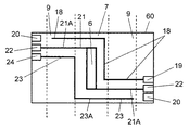
図18に、特許文献1で知られている、従来の圧電アクチュエータを用いた光学反射素子を示す。この光学反射素子は、ミラー部1と、ミラー部1と連結され、ミラー部1をX軸方向に駆動させる振動部2とを有している。また、振動部2と連結され、振動部2およびミラー部1を囲む枠体3を有している。また、枠体3と連結され、ミラー部1をY軸方向に駆動させる振動部4を有している。また、振動部4と連結され、振動部4および枠体3を囲む支持体5を有している。
FIG. 18 shows an optical reflecting element using a conventional piezoelectric actuator known from
振動部2および振動部4を駆動させるために、一般に、振動部2、振動部4は圧電素子(図示せず)を備えている。そしてこれらの圧電素子を駆動させるには、一般に、圧電素子毎に独立した駆動電極(図示せず)が配置されている。
In order to drive the
なお、この光学反射素子は、ミラー部1に光を入射すれば、その反射光をミラー部1の振動によってX軸、Y軸方向に走査させることができ、例えば壁やスクリーンに画像を投影することができる。
In addition, this optical reflection element can scan the reflected light in the X-axis and Y-axis directions by vibration of the
しかしながら、上記従来の光学反射素子は、電極配線数が多く、生産効率が低いという課題がある。 However, the conventional optical reflecting element has a problem that the number of electrode wirings is large and the production efficiency is low.
すなわち、従来の光学反射素子には、振動部2および振動部4をそれぞれ駆動させるために、それぞれ電気的に独立した駆動電極がパターニングされる。
That is, in the conventional optical reflecting element, in order to drive the
そしてこれらの駆動電極毎に配線電極が、振動部2および振動部4の表面を引き回されることから、素子上には複数の配線電極が引き回されることになる。したがって配線電極のパターニングは、素子の小型化に伴い、非常に複雑化し、生産効率低下の原因となる。
Since the wiring electrodes are routed around the surfaces of the vibrating
本発明は、配線電極数を減らし、生産効率を向上させることのできる圧電アクチュエータとこれを用いた光学反射素子および圧電駆動装置を提供するものである。 The present invention provides a piezoelectric actuator that can reduce the number of wiring electrodes and improve production efficiency, an optical reflection element using the piezoelectric actuator, and a piezoelectric driving device.
本発明の圧電アクチュエータは、第一駆動電極を有する第一圧電素子を備えた第一振動部と、第一振動部とは異なる中心軸を有し、第二駆動電極を有する第二圧電素子と、前記第一駆動電極および前記第二駆動電極に電気信号を印加する外部電極とを備え、前記外部電極に対して前記第一駆動電極と前記第二駆動電極が順に接続された構成を有する。 The piezoelectric actuator of the present invention includes a first vibrating portion with a first piezoelectric element having a first driving electrode, having a different central axis from the first vibrating portion, and a second piezoelectric element having a second driving electrode And an external electrode for applying an electric signal to the first drive electrode and the second drive electrode, and the first drive electrode and the second drive electrode are connected in order to the external electrode .
これにより本発明は、駆動電極の配線電極数が減り、引き回しが容易となり、結果として生産効率を向上させることができる。 Accordingly, the present invention reduces the number of wiring electrodes of the drive electrode, facilitates routing, and as a result, can improve production efficiency.
(実施の形態1)
図1に示すように、本実施の形態における光学反射素子60は、ミラー部6と、ミラー部6を介して対向するとともに、ミラー部6の各端部とそれぞれが連結された一対の振動部(第一振動部)7を有している。さらに、これらの振動部7と連結され、振動部7およびミラー部6の外周を囲む枠体8を有している。さらに、枠体8を介して対向するとともに、枠体8の各端部とそれぞれが連結された一対の振動部(第二振動部)9を有している。さらに、これらの振動部9と連結されるとともに、振動部9および枠体8の外周を囲う枠形状の支持体10を有している。
(Embodiment 1)
As shown in FIG. 1, the optical
なお、本実施の形態では、振動部7と振動部9とは、それぞれ異なる共振駆動周波数を有し、その周波数比は10倍〜100倍程度である。例えば本実施の形態では、振動部7の共振周波数が10kHz、振動部9の共振周波数が200Hz程度である。
In the present embodiment, the
振動部7の中心軸S1と振動部9の中心軸S2とは、それぞれ方向が異なり、交差する関係にある。本実施の形態では、振動部7はY軸に平行な中心軸S1を有し、振動部9はX軸に平行な中心軸S2を有している。また本実施の形態では、これらの中心軸S1、S2は、ミラー部6の重心で直交する関係にある。対となる振動部7は、振動部9の中心軸S2に対して線対称形であり、対となる振動部9は、振動部7の中心軸S1に対して線対称形である。
The central axis S1 of the
本実施の形態では、振動部7は繰り返し蛇行しながらY軸方向に延びるミアンダ形状を有する。振動部7は、X軸に平行(中心軸S1に垂直)な複数の振動板(第一振動板)7A〜7Dが、同一平面上で折り返し蛇行して連結されている。また、振動部9は繰り返し蛇行しながらX軸方向に延びるミアンダ形状を有する。振動部9は、Y軸方向に平行(中心軸S2に垂直)な複数の振動板(第二振動板)9A〜9Eが同一平面上で折り返し蛇行して連結されている。
In the present embodiment, the
図2は図1のP部(振動部7)を示す斜視図であり、図3はその3−3線断面図である。これらの図に示すように、振動部7を構成する複数の振動板7A〜7Dは、それぞれ、圧電素子(第一圧電素子)11とモニター素子(第一モニター素子)12とから構成される。
2 is a perspective view showing a P portion (vibration portion 7) of FIG. 1, and FIG. 3 is a sectional view taken along line 3-3. As shown in these drawings, each of the plurality of
振動部7における圧電素子11は、図3に示すように、ベースとなるシリコン基板14上に、シリコン酸化膜15を介して、振動部7と振動部9に共通に設けられた接地電極16を備えている。さらに、接地電極16上に振動部7と振動部9に共通に設けられた圧電層17を備えている。さらに、圧電層17上に設けられた駆動電極(第一駆動電極)18を備えている。駆動電極18は、図2に示すように、振動部7の複数の振動板7A〜7D上にそれぞれ配置された部分が共通接続された構成を有する。接地電極16は、図1に示す外部電極20と接続される。駆動電極18を有する圧電素子11を備えた振動部7が、中心軸S2を有する圧電アクチュエータを構成している。
As shown in FIG. 3, the
振動部7におけるモニター素子12は、図3に示すように、シリコン基板14上にシリコン酸化膜15を介して設けられた、圧電素子11と共通の接地電極16および圧電層17を備え、圧電層17上にモニター電極(第一モニター電極)21を備えている。モニター電極21は、図2に示すように、振動部7の複数の振動板7A〜7D上にそれぞれ配置された部分が共通接続された構成を有する。
As shown in FIG. 3, the
このように、振動部7を構成する各振動板7A〜7D上には、駆動電極18とモニター電極21の2本の電極が引き回される。また、モニター電極21は、図4、図5に示すように、幅狭の配線電極21Aとして、振動部9上を引き回され、図1の外部電極22と接続される。
In this way, the two electrodes of the
図4は図1のQ部(振動部9)を示す斜視図であり、図5はその5−5線断面図である。これらの図に示すように、振動部9を構成する複数の振動板9A〜9Eは、それぞれ、圧電素子(第二圧電素子)11とモニター素子(第二モニター素子)13とから構成される。
4 is a perspective view showing a Q portion (vibration portion 9) of FIG. 1, and FIG. 5 is a sectional view taken along line 5-5. As shown in these drawings, each of the plurality of
振動部9における圧電素子11は、図5に示すように、振動部7と同様に、ベースとなるシリコン基板14上に、シリコン酸化膜15を介して、振動部7と振動部9に共通に設けられた接地電極16を備えている。さらに、接地電極16上に振動部7と振動部9に共通に設けられた圧電層17を備えている。さらに、圧電層17上に設けられた駆動電極(第二駆動電極)18を備えている。駆動電極18は、図4に示すように、振動部9の複数の振動板9A〜9E上にそれぞれ配置された部分が共通接続された構成を有する。さらに、振動部7から引き回された駆動電極18と共通接続されると共に、図1に示す外部電極19と接続される。駆動電極18を有する圧電素子11を備えた振動部9が、中心軸S1を有する圧電アクチュエータを構成する。
As shown in FIG. 5, the
振動部9におけるモニター素子13は、図5に示すように、シリコン基板14上にシリコン酸化膜15を介して設けられた、圧電素子11と共通の接地電極16および圧電層17を備え、圧電層17上にモニター電極(第二モニター電極)23を備えている。モニター電極23は、図4に示すように、振動部9の複数の振動板9A〜9E上にそれぞれ配置された部分が共通接続された構成を有し、図1に示す外部電極24と接続されている。
As shown in FIG. 5, the
以上のように、本実施の形態では、振動部7に設けられたモニター電極21と、振動部9に設けられたモニター電極23とは電気的に独立している。したがって、上述したように、振動部9の複数の振動板9A〜9E上には、図5に示すように、駆動電極18とモニター電極23と振動部7の幅狭のモニター電極21の配線電極21Aとの3本の電極が引き回される。
As described above, in the present embodiment, the
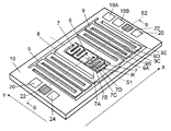
図6は、以上のような本実施の形態の光学反射素子の電極パターンを模式的に示した図である。図6では、光学反射素子60を、ミラー部6を中央に有する1つの振動部7と、振動部7を挟む2つの振動部9とで示している。駆動電極18は、振動部7、9に配置され、外部電極19に共通に接続された1本の電極として示されている。振動部7上に配置されたモニター電極21は、モニター電極23とは独立しており、振動部9上を引き回され2つの外部電極22に接続されていることを示している。一対の振動部9上に配置されたモニター電極23は、モニター電極21とは独立しており、振動部7上を配線電極23Aで引き回されて、外部電極24に共通に接続されていることを示している。
FIG. 6 is a diagram schematically showing the electrode pattern of the optical reflecting element of the present embodiment as described above. In FIG. 6, the
このように、振動部7の各振動板7A〜7D上では、図3に示すのと同様に、駆動電極18とモニター電極21が設けられている。また、振動部9の各振動板9A〜9E上では、図5に示すのと同様に、モニター電極21の配線電極21Aを挟んで駆動電極18とモニター電極23が設けられている。
Thus, on each
なお、本実施の形態では、図6に示すように、共通の駆動電極18の終端は開放としたが、外部電極を別途設け、その外部電極に引き出してもよい。
In the present embodiment, as shown in FIG. 6, the end of the
また、本実施の形態では、ベースとしてシリコン基板14を用いたが、その他酸化マグネシウム(MgO)あるいはステンレスなどの板を用いてもよい。また接地電極16はプラチナ、駆動電極18およびモニター電極21、23は金、圧電層17はチタン酸ジルコン酸鉛(Pb(ZrX,Ti1−X)O3で、x=0.525)などが挙げられる。これらの電極の材料は、蒸着、ゾル、ゲル、CVD、スパッタ法などによって薄膜化することができる。
In this embodiment, the
次に、図7を用いて本実施の形態の圧電駆動装置の構成について説明する。図7は、本発明の一実施の形態における圧電駆動装置の構成を示すブロック図である。 Next, the configuration of the piezoelectric drive device of the present embodiment will be described with reference to FIG. FIG. 7 is a block diagram showing the configuration of the piezoelectric drive device according to one embodiment of the present invention.
本実施の形態の圧電駆動装置は、図1に示した光学反射素子60と、光学反射素子60の振動部7および振動部9にそれぞれの共振駆動信号を入力する駆動装置61とを備えるものである。
The piezoelectric drive device according to the present embodiment includes the
本実施の形態の駆動装置61は、並列配置された増幅器25、26を有している。増幅器25はインピーダンス素子27と接続され、増幅器26はインピーダンス素子28と接続されている。そして増幅器25とインピーダンス素子27とをつなぐ配線と、増幅器26とインピーダンス素子28とをつなぐ配線とは共通接続されて、図1に示す光学反射素子60の外部電極19に接続される。外部電極19からは共通の配線電極18Aが光学反射素子60上を引き回され、振動部7、9の駆動電極18に接続される。
The
一方、振動部7の振動を検出するモニター電極21は、配線電極21Aとして光学反射素子60上を引き回されて外部電極22に接続され、外部電極22から外部に引き出され、駆動装置61のフィルター29を介して増幅器25と接続される。また、振動部9の振動を検出するモニター電極23は、配線電極23Aとして光学反射素子60上を引き回されて外部電極24に引き回され、外部電極24から外部に引き出され、駆動装置61のフィルター30を介して増幅器26と接続される。
On the other hand, the
次に、本実施の形態における光学反射素子の動作を図7を用いて説明する。まず、図7に示すように、増幅器25の入力端子25Aに振動部7を駆動させる電気信号(交流電圧)が入力され、増幅される。また増幅器26の入力端子26Aに振動部9を駆動させる電気信号(交流電圧)が入力され、増幅される。
Next, the operation of the optical reflecting element in the present embodiment will be described with reference to FIG. First, as shown in FIG. 7, an electric signal (alternating voltage) for driving the
なお、本実施の形態では、振動部7には、この振動部7に固有の振動周波数を有する電気信号を入力し、振動部7を共振駆動させている。また振動部9には、この振動部9に固有の振動周波数を有する電気信号を入力し、振動部9を共振駆動させている。これにより、振動部7および振動部9を効率よく駆動させることができ、大きく変位させることができる。
In the present embodiment, an electric signal having a vibration frequency unique to the
上述の電気信号は、それぞれ抵抗器などのインピーダンス素子27、28を介して合成され、光学反射素子60の外部電極19に供給される。合成された電気信号は、外部電極19から引き回され、一本の配線電極18Aを介して振動部9および振動部7上の駆動電極18に流れ(図6参照)、それぞれの圧電素子11を共に駆動させる。
The above electric signals are combined via
すなわち本実施の形態では、振動部9は、共通の駆動電極18から供給される交流電圧の正・負によって上下に(素子平面に対して垂直方向に)振動する。この振動によって、図1に示す枠体8の下端部(振動部9と連結される部分)が上下(素子平面に対して垂直方向)に振動し、ミラー部6の中心を不動点としながらミラー部6を、中心軸S2を中心に回動させる。なお、本実施の形態において、振動部9の中心軸S2は、この振動部9の駆動によるミラー部6の回転軸と一致する。
In other words, in the present embodiment, the
また、同様に、振動部7は、共通の駆動電極18から供給される交流電圧の正・負によって上下に振動する。この振動によって、図1に示すミラー部6の側端部(振動部7と連結される部分)が上下(素子平面に対して垂直方向)に振動し、ミラー部6の中心を不動点としながら、ミラー部6を、中心軸S1を中心に回動させる。振動部7の中心軸S1は、この振動部7の駆動によるミラー部6の回転軸と一致する。
Similarly, the
振動部7上に配置されたモニター電極21は、振動部7の変位を電気信号として検知し、その電気信号は、配線電極21Aを介して外部電極22から外部に引き出される。また、振動部9上に配置されたモニター電極23は、振動部9の変位を電気信号として検知し、その電気信号は、配線電極23Aを介して外部電極24から外部に引き出される。
The
外部電極22から引き出された電気信号は、図7に示すように、駆動装置61のフィルター29を介して取り出され、再び増幅器25に入力端子25Aに入力される。また、外部電極24から引き出された電気信号は、駆動装置61のフィルター30を介して取り出され、再び増幅器26の入力端子26Aに入力される。
As shown in FIG. 7, the electrical signal drawn from the
このようにそれぞれのモニター電極21、23から出力される電気信号を、振動部7、振動部9の各圧電素子11の駆動電極18にフィードバックすることにより、光学反射素子を自励駆動させることが出来る。
Thus, by feeding back the electric signals output from the
なお、インピーダンス素子27、28としては、上述の抵抗器以外にも、コンデンサやコイルなどのリアクタンス素子、あるいはこれらの組み合わせ等も挙げられる。
In addition, as the
また、本実施の形態では、外部電極19に2つの電気信号を合成して入力したが、3つ以上の電気信号を合成することも可能である。
In the present embodiment, two electric signals are combined and input to the
以上のように、本実施の形態では、駆動電極18の配線電極数を減らし、生産効率を向上させることができる。
As described above, in the present embodiment, the number of wiring electrodes of the
すなわち従来の光学反射素子は、電極パターンの効率化について考慮されておらず、図18に示す振動部2および振動部4をそれぞれ駆動させるために、これらの振動部2および振動部4上には、個々に独立した駆動電極がパターニングされていた。したがって、光学反射素子上には、これらの駆動電極毎に配線電極を引き回す必要があった。すなわち、少なくとも振動部4には、この振動部4の駆動電極と、振動部2の駆動電極の配線電極とを引き回さなければならなかった。
That is, in the conventional optical reflecting element, the efficiency of the electrode pattern is not taken into consideration, and in order to drive the vibrating
この配線電極の数が増えると、駆動電極や配線電極のパターニングが困難となる。特に小型の光学反射素子の場合や、モニター電極を形成する場合、微小領域に複数の電極や配線電極をパターニングすることになり、パターニングが非常に困難となる。また、本実施の形態のように、振動部7、9が複雑なミアンダ形状の場合は、特に電極等のパターニングが難しくなり、生産効率低下の原因となっていた。
As the number of wiring electrodes increases, it becomes difficult to pattern drive electrodes and wiring electrodes. In particular, in the case of a small optical reflection element or when a monitor electrode is formed, a plurality of electrodes and wiring electrodes are patterned in a minute region, which makes patterning very difficult. Moreover, when the vibrating
これに対し本実施の形態では、複数の電気信号を合成したため、一つの駆動電極18で複数の電気信号を供給できる。すなわち、共通の駆動電極18で振動部7および振動部9を共に駆動させることができる。
In contrast, in the present embodiment, since a plurality of electrical signals are synthesized, a plurality of electrical signals can be supplied by one
したがって、振動部7、9の駆動電極18の配線電極も共通になるため、駆動電極18の配線電極数を減らすことができ、結果として生産効率を向上させることが出来る。
Accordingly, since the wiring electrodes of the driving
また、複数の電気信号は、インピーダンス素子27、28を介した後合成したため、電気信号間において、たとえば周波数の差が大きくても容易に合成することができる。
In addition, since the plurality of electrical signals are synthesized after passing through the
また、本実施の形態では、振動部7および振動部9をミアンダ形状としたことにより、光学反射素子全体として小型化を図りながらも共振器長を長く調整することができ、ミラー部6の変位を大きくすることができる。
Further, in the present embodiment, since the vibrating
また本実施の形態では、振動部7および振動部9を共に共振させることにより、ミラー部6の変位を大きくすることができる。
In the present embodiment, the displacement of the
さらに本実施の形態では、図1に示すように、振動部7はミラー部6の側端部と連結されていることから、てこの原理によりミラー部6を、中心軸S1を中心に大きく回動させることができる。同様に、振動部9は枠体8の下端部と連結されていることから、ミラー部6を、中心軸S2を中心に、大きく回動させることができる。
Further, in the present embodiment, as shown in FIG. 1, since the vibrating
また、振動部7、9は、それぞれミラー部6および枠体8の端部と連結させているため、ミラー部6の中心が不動点となり、この不動点においては、入射光と反射光との光路長が一定に保たれるため、この光学反射素子により投影する画像の歪みを抑制することができる。
Moreover, since the
なお、本実施の形態では、図6に示すように、共通の駆動電極18は一対の振動部9両方に引き回したが、図8に示すように、一方の振動部9に引き回してもよい。この場合も、一方(例えば、ミラー部6に対して右側)の振動部9に印加された振動が、枠体8(図1参照)を介して他方(ミラー部6に対して左側)の振動部9に伝搬し、共振させることができ、結果としていずれの振動部9をも振動させることができる。
In the present embodiment, as shown in FIG. 6, the
また、駆動電極18を一方の振動部9に形成する場合は、図8に示すように、振動部9の振幅を検知するモニター電極23を、駆動電極18が引き回されていない左側の振動部9にのみ形成してもよい。
Further, when the
この場合、モニター電極23が引き回されない右側の振動部9においては、駆動電極18と、振動部7のモニター電極21の配線電極21Aとが形成されることになる。なおこの時、図8、図9に示すように、共通の駆動電極18を、振動部9の各振動板9A〜9E上の両側に分けて左右対称に配置し、その中央にモニター電極21の配線電極21Aを配置することができる。なお分岐させた駆動電極18は、ジャンパー線などで適宜接続させればよい。
In this case, the
このように、各振動板9A〜9E上において、駆動電極18を左右対称に配置することによって、振動部9上に均一に電圧を印加することができ、振動部9を垂直に振動させることが出来る。
As described above, by arranging the
また、図8に示すように、左側の振動部9においては、この振動部9の振幅を検知するためのモニター電極23を、振動部9の各振動板9A〜9E上の両側に分けて左右対称に配置することができる。これにより振動部9の面積を効率よく利用でき、モニター電極23の感度を向上させることが出来る。なお、二分したモニター電極23は、ジャンパー線などで適宜電気的に接続させることが出来る。
Further, as shown in FIG. 8, in the
なお、本実施の形態では、一対の振動部7のいずれにも駆動電極18を配置したが、一方の振動部7に駆動電極18を配置し、共振駆動させれば、その振動がミラー部6を介して他方の振動部7に伝搬し、この他方の振動部7も共振駆動させることができる。したがって、振動部7の駆動電極18の配線電極数を減らすことができる。
In the present embodiment, the
(実施の形態2)
図10は本発明の実施の形態2における光学反射素子の電極パターンを模式的に示した図である。本実施の形態と実施の形態1との主な違いは、図10に示すように、電気的に独立した二つの駆動電極31、32を振動部7に設けた点である。駆動電極31、32には、それぞれ外部電極19A、19Bを介して、正負逆位相の交流電圧を印加する。
(Embodiment 2)
FIG. 10 is a diagram schematically showing an electrode pattern of the optical reflecting element according to
図11は本実施の形態の光学反射素子を示す斜視図である。図12は図11のR部の断面図である。図10〜図12に示すように、本実施の形態では、振動部7の複数の振動板7A〜7D上には、電気的に独立した二つの駆動電極31、32を交互に配置している。これらの駆動電極31、32をそれぞれ共通接続するため、複数の振動板7A〜7D上には、電気的に独立した二つの駆動電極31、32の配線電極31A、32Aも交互に配置している。
FIG. 11 is a perspective view showing the optical reflecting element of the present embodiment. FIG. 12 is a cross-sectional view of a portion R in FIG. As shown in FIGS. 10 to 12, in the present embodiment, two electrically
すなわち、図12に示すように、振動部7において、駆動電極31が配置された振動板7A、7C上には、幅狭に形成された駆動電極32の配線電極32Aが引き回されている。駆動電極32が配置された振動板7B、7D上には、幅狭に形成された駆動電極31の配線電極31Aが引き回されている。
That is, as shown in FIG. 12, in the
このように、駆動電極31、32を交互に配置し、これらの駆動電極31、32に正負逆位相の交流電圧を印加すれば、各振動板7A〜7Dの曲げ方向は交互に逆向きとなり、図13にその振動状態を示すように、振動の変位は蓄積される。したがって、振動部7全体としては、中心軸S1を回転軸とし、大きく反復回動させることができ、結果としてミラー部6の変位(振幅)を大きくすることができる。
As described above, when the
また、図10に示すように、本実施の形態では、振動部9上には、実施の形態1と同様に、それぞれの振動板9A〜9E(図11参照)上に共通の駆動電極31を配置している。
As shown in FIG. 10, in the present embodiment, a
すなわち本実施の形態では、一方の駆動電極31は、振動部7と振動部9との圧電素子に共通の駆動電極31とし、他方の駆動電極32は振動部7の圧電素子のみを駆動させる駆動電極32として用いている。したがって、振動部9のそれぞれの振動版9A〜9E上には、駆動電極31以外に駆動電極32の配線電極32Aも引き回されている。なお、本実施の形態では、振動部7では、2つの駆動電極31、32が形成されるため、モニター電極21は実施の形態1より狭幅となる。
That is, in the present embodiment, one
なお、本実施の形態では、振動部7のモニター電極21は、外部電極22から振動部9を介して振動部7に引き回したため、振動部9には、実施の形態1よりも幅狭のモニター電極21の配線電極21Aが形成されている。また振動部9のモニター電極23は、外部電極24から各振動部9に引き回した。ここでモニター電極23の配線電極は、振動部7上には引き回さず、枠体8を介して一対の振動部9にそれぞれ引き回してもよい。
In the present embodiment, the
本実施の形態では、駆動電極31に、振動部7と振動部9のそれぞれの共振駆動信号を合成した電気信号を入力することで、駆動電極31を振動部7と振動部9に共通の駆動電極31とすることができ、電極配線の数を減らすことができる。
In the present embodiment, an electric signal obtained by synthesizing the resonance drive signals of the
なお、本実施の形態の光学反射素子を画像投影装置に用いる場合、高精度な画像を投影するには、一般的にX軸方向の走査速度はY軸方向の走査速度よりもはるかに大きくする必要がある。 When the optical reflecting element according to the present embodiment is used in an image projection apparatus, in order to project a highly accurate image, generally, the scanning speed in the X-axis direction is much higher than the scanning speed in the Y-axis direction. There is a need.
この場合、X軸方向に振動する振動部7の周波数を高くすればよいが、周波数が高くなるほど、ミラー部6の変位が小さくなる。したがって本実施の形態のように、振動部7の振動板7A〜7D上には、二つの駆動電極31、32を交互に配置し、それぞれの駆動電極31、32に逆位相の電圧を印加することで、変位を蓄積し、大きな振幅を得ることができる。さらに、振動部9と振動部7とは駆動電極31を共通させることで、従来のような配線電極数の増加を回避でき、高性能の光学反射素子の生産効率の向上を図ることができる。
In this case, the frequency of the
その他、実施の形態1と同様の構成から得られる効果については実施の形態と同じであるので説明を省略する。 The other effects obtained from the same configuration as in the first embodiment are the same as those in the first embodiment, and thus the description thereof is omitted.
(実施の形態3)
図14は、本発明の実施の形態3における光学反射素子の電極パターンを模式的に示した図である。本実施の形態と実施の形態1との違いは、図14に示すように、振動部7および振動部9のモニター素子は、共通のモニター電極33を有し、これらのモニター電極33は、図15に示すように、共通の配線電極33Aで外部電極34から引き出される点である。
(Embodiment 3)
FIG. 14 is a diagram schematically showing an electrode pattern of the optical reflecting element according to
また、本実施の形態では、振動部7の圧電素子11を駆動させる駆動電極35と、振動部9の圧電素子を駆動させる駆動電極36とは個々に形成し、電気的に独立させている。したがって、これらの駆動電極35、36の配線電極35A、36Aは、それぞれ個々に引き回している。
In the present embodiment, the
本実施の形態では、図15に示すように、振動部7の圧電素子の駆動により発生した電気信号と、振動部9の圧電素子の駆動により発生した電気信号とは、混在した状態で共通のモニター電極33で感知される。混在した電気信号は、外部電極34からフィルター37Aを介することによって、振動部7で発生した電気信号のみが取り出される。また、フィルター37Bを介することによって、振動部9で発生した電気信号のみが取り出される。このようにして、本実施の形態によれば、共通のモニター電極33で感知された電気信号を、個々の電気信号に分離検出することができる。
In the present embodiment, as shown in FIG. 15, the electric signal generated by driving the piezoelectric element of the vibrating
これにより本実施の形態では、従来電気的に独立させていた二つのモニター電極を、共通にすることができ、一つの配線電極33Aで引き出すことができる。すなわち電極配線の数が減り、結果としてパターニングが簡易になり、生産効率を向上させることができる。
As a result, in the present embodiment, two monitor electrodes that have been conventionally electrically independent can be made common and can be drawn out by one
なお、上記実施の形態では、振動部7と振動部9とで駆動電極35、36は共通にしていないが、駆動電極35、36も共通にしてもよい。これにより、駆動電極35、36の電極配線数も減らすことができる。
In the above embodiment, the
また本実施の形態の別の例として、一方の振動部7(例えば、図1の下方の振動部7)および一方の振動部9(例えば、図1の右側の振動部9)とに共通の駆動電極を形成し、他方の振動部7(例えば、図1の上方の振動部7)と振動部9(例えば、図1の左側の振動部9)とに共通のモニター電極を形成してもよい。
Further, as another example of the present embodiment, it is common to one vibration part 7 (for example, the
これにより各一方の振動部7および振動部9上には駆動電極を、各他方の振動部7および振動部9上にはモニター電極を形成すればよいため、パターニングがより簡易となる。なお、これとは逆に、一方の振動部7および一方の振動部9とに共通のモニター電極を形成し、他方の振動部7と振動部9とに共通の駆動電極を形成してもよい。
As a result, a drive electrode may be formed on each of the one
その他、実施の形態1と同様の構成から得られる効果については実施の形態と同じであるので説明を省略する。 The other effects obtained from the same configuration as in the first embodiment are the same as those in the first embodiment, and thus the description thereof is omitted.
(実施の形態4)
図16は、本発明の実施の形態4における圧電駆動装置の構成を示すブロック図である。本実施の形態と実施の形態1との主な違いは、圧電駆動装置に電気信号を合成する合成回路を設けた点である。
(Embodiment 4)
FIG. 16 is a block diagram showing the configuration of the piezoelectric drive device according to Embodiment 4 of the present invention. The main difference between the present embodiment and the first embodiment is that a synthesis circuit for synthesizing electrical signals is provided in the piezoelectric drive device.
図16に示すように、本実施の形態における駆動制御装置62は、2つの前置アンプ(第一前置アンプ、第二前置アンプ)38、39が並列に配置されている。前置アンプ38は飽和アンプ(第一飽和アンプ)40と電気的に接続され、飽和アンプ40は帯域フィルター41(第一帯域フィルター)と電気的に接続され、帯域フィルター41から振動部7の共振駆動信号(第一電気信号)が取り出される。
As shown in FIG. 16, in the
同様に、前置アンプ39は飽和アンプ(第二飽和アンプ)42と電気的に接続され、飽和アンプ42は帯域フィルター(第二帯域フィルター)43と電気的に接続され、帯域フィルター43から振動部9の共振駆動信号(第二電気信号)が取り出される。
Similarly, the
なお、飽和アンプ40、42としては、出力が所定値に達すると、その値を維持する飽和型アンプ、あるいは出力が所定値に達すると、出力を減衰させる負性飽和型アンプ等を用いることができる。
As the
これらの飽和アンプ40と帯域フィルター41、または飽和アンプ42と帯域フィルター43とを通過して出力された各共振駆動信号は、加算器44等を含む加算合成回路45で合成される。加算合成回路45から出力された信号は、外部電極19から光学反射素子60を引き回され、振動部7および振動部9に共通の駆動電極18に入力される。
Resonance drive signals output after passing through the
また、本実施の形態では、振動部7の振動振幅によって発生した電気信号を、モニター電極21で検出し、前置アンプ38に帰還する帰還回路を構成している。ここで本実施の形態では、この帰還回路における閉ループゲインが1以上となるよう、すなわちモニター電極21から出力された信号が、前置アンプ38に入力された信号より減衰しないよう、振動部7の駆動周波数と帯域フィルター41の通過周波数帯域を設定した。また、加算合成回路45で合成するのは3つ以上の電気信号でもよい。
Further, in the present embodiment, an electric signal generated by the vibration amplitude of the
また、この振動部7と同様に、振動部9の振動振幅によって発生した電気信号を、モニター電極23で検出し、前置アンプ39へと帰還している。本実施の形態では、この帰還回路における閉ループゲインも1以上となるように振動部9の駆動周波数と帯域フィルター43の通過周波数帯域を設定した。
Similarly to the vibrating
次に、本実施の形態の光学反射素子の駆動方法を説明する。図16に示すように、まず、振動部7を駆動させる電気信号(交流電圧)が前置アンプ38の入力端子38Aに入力されると、この信号が前置アンプ38で増幅される。次に前置アンプ38で増幅された信号が飽和アンプ40に入力され、所定レベルの信号に矯正される。飽和アンプ40から出力された信号は帯域フィルター41に入力され、振動部7の共振駆動信号が取り出される。
Next, a method for driving the optical reflecting element of the present embodiment will be described. As shown in FIG. 16, first, when an electrical signal (AC voltage) for driving the
また、同様に、前置アンプ39の入力端子39Aに振動部9を駆動させる電気信号(交流電圧)が入力され、増幅される。増幅された信号は、飽和アンプ42で矯正され、その後帯域フィルター43に入力され、振動部9の共振駆動信号が取り出される。
Similarly, an electric signal (AC voltage) for driving the
これらの振動部7および振動部9から取り出された共振駆動信号が、加算合成回路45で合成される。合成された電気信号は、光学反射素子60の外部電極19から引き回され、駆動電極18に流れ、振動部9および振動部7を同時に駆動させる。
The resonance drive signals taken out from the
また、図16に示すように、モニター電極21は、振動部7の振動振幅により電圧を検知し、その電気信号は外部電極22から引き出される。一方、モニター電極23は、振動部9の振動振幅により電圧を検知し、その電気信号は外部電極24から引き出される。これら外部電極22、24から引き出された電気信号は、前置アンプ38および前置アンプ39にそれぞれ帰還される。
Further, as shown in FIG. 16, the
なお、光学反射素子60の振動部7あるいは振動部9を、信号に追従させて共振駆動させるには、印加する駆動周波数の位相ずれを、±70deg以内の範囲とすることが好ましい。
In addition, in order to drive the
したがって、本実施の形態では、帯域フィルター41は、その通過帯域が、振動部7において位相範囲が±70deg以内に相当する周波数帯域となるように制御した。また同様に、帯域フィルター43は、その通過帯域が、振動部9において位相範囲±70deg以内に相当する周波数帯域となるように制御した。
Therefore, in the present embodiment, the
なお本実施の形態では、振動部7および振動部9がそれぞれ位相範囲±70degで駆動したかどうかをモニター電極21またはモニター電極23で検知し、加算合成回路45に入力される各信号を所定値に制御する手段をさらに設けてもよい。
In the present embodiment, the
本実施の形態では、実施の形態1と同様に、駆動電極18の電極配線数を低減することができ、簡易な配線パターンとすることができる。
In the present embodiment, similarly to the first embodiment, the number of electrode wires of the
また本実施の形態では、前置アンプ38、39、飽和アンプ40、42、帯域フィルター41、43、加算合成回路45はいずれも能動素子からなるため、これらはICチップ化することができ、実装工程における合理化が図れる。
In the present embodiment, the
なお、本実施の形態では、振動部7および振動部9のそれぞれの振動板(図1の7A〜7D,9A〜9E)上に共通の駆動電極18を配置したが、例えば振動部7または振動部9のいずれか一方、あるいは双方の振動板上に、二種類の駆動電極を交互に配置してもよい。この場合は、実施の形態2で説明したように、各駆動電極に正負逆位相の電圧を印加することにより、変位が蓄積され、大きな振幅を得ることができる。
In the present embodiment, the
また、本実施の形態では、振動部7、振動部9の各振動板上に駆動電極18を配置しているが、駆動電極18の配置場所はこれに限定されず、例えば振動部7および振動部9には、それぞれ一部の振動板上に駆動電極18を配置してもよい。
Further, in the present embodiment, the
図17は、本実施の形態1〜4の光学反射素子を用いた画像投影装置を示す構成図である。図17に示すように、本実施の形態の画像投影装置は、レーザ光源などの光源46と光学反射素子60とスクリーン49とから構成される。
FIG. 17 is a configuration diagram illustrating an image projection apparatus using the optical reflecting elements according to the first to fourth embodiments. As shown in FIG. 17, the image projection apparatus according to the present embodiment includes a
この構成によれば、光源46から光学反射素子60のミラー部6へ入射光47を入射し、ミラー部6からの反射光48を、スクリーン49に投影する。このとき、ミラー部6を振動させることによって、反射光48をX軸、Y軸方向に走査させることができ、スクリーン49や壁に画像50、文字等を投影することができる。
According to this configuration, the
なお、実施の形態1〜4の光学反射素子では、振動部7、9の形状をミアンダ形としたが、これに限定されず、その他、例えばカンチレバー形、十字形等、各種形状でも応用が可能である。
In the optical reflecting elements of the first to fourth embodiments, the shape of the vibrating
また、実施の形態1〜4では、振動部7、9から構成される圧電アクチュエータは、ミラー部6が連結されて光学反射素子として用いていた。しかし、この圧電アクチュエータは、例えばミラー部の代わり発光素子を連結させ、光学デバイスとして用いることもできる。
In the first to fourth embodiments, the piezoelectric actuator including the vibrating
本発明の光学反射素子は、配線電極数を減らすことで、複雑な形状の振動部上にも容易に形成することができ、小型のプロジェクタやヘッドアップディスプレイ、ヘッドマウントディスプレイなど、小型画像投影装置に有用である。 The optical reflecting element of the present invention can be easily formed on a vibration part having a complicated shape by reducing the number of wiring electrodes, and a small image projecting device such as a small projector, a head-up display, or a head-mounted display. Useful for.
6 ミラー部
7,9 振動部
7A〜7D,9A〜9E 振動板
8 枠体
10 支持体
11 圧電素子
12,13 モニター素子
14 シリコン基板
15 シリコン酸化膜
16 接地電極
17 圧電層
18,31,32,35,36 駆動電極
18A,21A,23A,31A,32A,33A,35A,36A 配線電極
19,19A,19B,20,22,24,34 外部電極
25,26 増幅器
27,28 インピーダンス素子
29,30,37A,37B フィルター
38,39 前置アンプ
40,42 飽和アンプ
41,43 帯域フィルター
44 加算器
45 加算合成回路
46 光源
47 入射光
48 反射光
49 スクリーン
50 画像
60 光学反射素子
61 駆動装置
62 駆動制御装置
S1,S2 中心軸
6 Mirror
Claims (7)
Priority Applications (1)
| Application Number | Priority Date | Filing Date | Title |
|---|---|---|---|
| JP2009529976A JP5347963B2 (en) | 2007-08-27 | 2008-08-20 | Piezoelectric actuator, optical reflection element using the same, and piezoelectric drive device |
Applications Claiming Priority (6)
| Application Number | Priority Date | Filing Date | Title |
|---|---|---|---|
| JP2007219509 | 2007-08-27 | ||
| JP2007219509 | 2007-08-27 | ||
| JP2008020471 | 2008-01-31 | ||
| JP2008020471 | 2008-01-31 | ||
| JP2009529976A JP5347963B2 (en) | 2007-08-27 | 2008-08-20 | Piezoelectric actuator, optical reflection element using the same, and piezoelectric drive device |
| PCT/JP2008/002246 WO2009028152A1 (en) | 2007-08-27 | 2008-08-20 | Piezoelectric actuator, optical reflection element using the same and piezoelectric driver |
Publications (2)
| Publication Number | Publication Date |
|---|---|
| JPWO2009028152A1 JPWO2009028152A1 (en) | 2010-11-25 |
| JP5347963B2 true JP5347963B2 (en) | 2013-11-20 |
Family
ID=40386895
Family Applications (1)
| Application Number | Title | Priority Date | Filing Date |
|---|---|---|---|
| JP2009529976A Active JP5347963B2 (en) | 2007-08-27 | 2008-08-20 | Piezoelectric actuator, optical reflection element using the same, and piezoelectric drive device |
Country Status (5)
| Country | Link |
|---|---|
| US (1) | US8437061B2 (en) |
| JP (1) | JP5347963B2 (en) |
| CN (1) | CN101790840B (en) |
| TW (1) | TWI470271B (en) |
| WO (1) | WO2009028152A1 (en) |
Families Citing this family (24)
| Publication number | Priority date | Publication date | Assignee | Title |
|---|---|---|---|---|
| WO2010122751A1 (en) * | 2009-04-21 | 2010-10-28 | パナソニック株式会社 | Optical reflection element |
| JP5444968B2 (en) | 2009-05-11 | 2014-03-19 | ミツミ電機株式会社 | Actuator and optical scanning device using the same |
| JP2010263736A (en) * | 2009-05-11 | 2010-11-18 | Mitsumi Electric Co Ltd | Piezoelectric actuator |
| JP5611565B2 (en) * | 2009-10-27 | 2014-10-22 | スタンレー電気株式会社 | Piezoelectric vibration generator and power generator using the same |
| JP5471946B2 (en) | 2010-08-02 | 2014-04-16 | 船井電機株式会社 | Vibration mirror element |
| CN101976013A (en) * | 2010-09-30 | 2011-02-16 | 上海理工大学 | Projector with function of eliminating laser speckles |
| JP5987510B2 (en) * | 2011-10-03 | 2016-09-07 | ミツミ電機株式会社 | Optical scanning device and optical scanning control device |
| JP5779472B2 (en) * | 2011-10-07 | 2015-09-16 | スタンレー電気株式会社 | Optical deflector |
| WO2013114857A1 (en) * | 2012-01-31 | 2013-08-08 | パナソニック株式会社 | Piezoelectric actuator device and method for manufacturing same |
| JP5864311B2 (en) * | 2012-03-12 | 2016-02-17 | スタンレー電気株式会社 | Optical deflector |
| JPWO2013136759A1 (en) | 2012-03-15 | 2015-08-03 | パナソニックIpマネジメント株式会社 | Optical reflection element and actuator |
| JP2013200337A (en) * | 2012-03-23 | 2013-10-03 | Stanley Electric Co Ltd | Light deflector |
| JP2013205818A (en) * | 2012-03-29 | 2013-10-07 | Stanley Electric Co Ltd | Light deflector |
| WO2014068846A1 (en) * | 2012-10-31 | 2014-05-08 | パナソニック株式会社 | Actuator |
| JP6123290B2 (en) * | 2012-12-26 | 2017-05-10 | 株式会社リコー | Piezoelectric actuator device, two-dimensional scanning device, image forming device, and image projection device |
| JP6264709B2 (en) * | 2013-12-25 | 2018-01-24 | スタンレー電気株式会社 | Vehicle lighting |
| JP2015132762A (en) * | 2014-01-15 | 2015-07-23 | 株式会社リコー | Optical deflector, image forming apparatus, and image projection device |
| JP6398454B2 (en) | 2014-08-13 | 2018-10-03 | セイコーエプソン株式会社 | Piezoelectric drive device, robot, and drive method thereof |
| RU2720478C2 (en) * | 2015-06-03 | 2020-04-30 | Конинклейке Филипс Н.В. | Device with actuator based on electroactive polymer |
| JP6662392B2 (en) | 2015-12-22 | 2020-03-11 | 株式会社リコー | Rotating device, optical scanning device, and image display device |
| DE102018215528A1 (en) * | 2018-09-12 | 2020-03-12 | Robert Bosch Gmbh | Micromechanical component and manufacturing method for a micromechanical component |
| CN109794405A (en) * | 2019-02-18 | 2019-05-24 | 河南中医药大学 | High intensity focused ultrasound signal calibration circuit |
| CN112817141B (en) * | 2020-12-31 | 2023-03-24 | 歌尔股份有限公司 | MEMS scanning mirror, driving method thereof and laser projector |
| CN112782845B (en) * | 2020-12-31 | 2023-02-21 | 歌尔股份有限公司 | MEMS scanning mirror and laser projector |
Citations (6)
| Publication number | Priority date | Publication date | Assignee | Title |
|---|---|---|---|---|
| JPH09101474A (en) * | 1995-10-06 | 1997-04-15 | Denso Corp | Optical scanner device |
| JP2001111672A (en) * | 1999-10-05 | 2001-04-20 | Kenwood Corp | Mobile communication terminal |
| JP2003181800A (en) * | 2001-12-19 | 2003-07-02 | Hitachi Ltd | Piezoelectric micro-actuator and micro-mirror equipped with the same |
| JP2004237400A (en) * | 2003-02-06 | 2004-08-26 | Nippon Signal Co Ltd:The | Planar-type actuator |
| JP2005148459A (en) * | 2003-11-17 | 2005-06-09 | Stanley Electric Co Ltd | Two dimensional optical scanner and optical device |
| JP2008035600A (en) * | 2006-07-27 | 2008-02-14 | Stanley Electric Co Ltd | Piezoelectric actuator and its manufacturing method |
Family Cites Families (6)
| Publication number | Priority date | Publication date | Assignee | Title |
|---|---|---|---|---|
| JP3050130B2 (en) * | 1996-07-31 | 2000-06-12 | 日本電気株式会社 | Piezoelectric transformer and its abnormal operation detection and protection device |
| JP2003089206A (en) * | 2001-09-19 | 2003-03-25 | Sharp Corp | Method for driving ink jet head and ink jet printer |
| JP4531470B2 (en) * | 2004-07-26 | 2010-08-25 | Hoya株式会社 | Hinge structure |
| US7356880B2 (en) | 2004-07-26 | 2008-04-15 | Pentax Corporation | Hinge structure of micromirror device |
| JP4328980B2 (en) * | 2006-12-18 | 2009-09-09 | セイコーエプソン株式会社 | Piezoelectric vibrator and manufacturing method thereof, MEMS device and manufacturing method thereof |
| JP4317231B2 (en) * | 2007-02-16 | 2009-08-19 | 富士通株式会社 | Micromirror device and manufacturing method thereof |
-
2008
- 2008-08-20 JP JP2009529976A patent/JP5347963B2/en active Active
- 2008-08-20 US US12/673,238 patent/US8437061B2/en active Active
- 2008-08-20 WO PCT/JP2008/002246 patent/WO2009028152A1/en active Application Filing
- 2008-08-20 CN CN2008801046486A patent/CN101790840B/en active Active
- 2008-08-25 TW TW97132360A patent/TWI470271B/en not_active IP Right Cessation
Patent Citations (6)
| Publication number | Priority date | Publication date | Assignee | Title |
|---|---|---|---|---|
| JPH09101474A (en) * | 1995-10-06 | 1997-04-15 | Denso Corp | Optical scanner device |
| JP2001111672A (en) * | 1999-10-05 | 2001-04-20 | Kenwood Corp | Mobile communication terminal |
| JP2003181800A (en) * | 2001-12-19 | 2003-07-02 | Hitachi Ltd | Piezoelectric micro-actuator and micro-mirror equipped with the same |
| JP2004237400A (en) * | 2003-02-06 | 2004-08-26 | Nippon Signal Co Ltd:The | Planar-type actuator |
| JP2005148459A (en) * | 2003-11-17 | 2005-06-09 | Stanley Electric Co Ltd | Two dimensional optical scanner and optical device |
| JP2008035600A (en) * | 2006-07-27 | 2008-02-14 | Stanley Electric Co Ltd | Piezoelectric actuator and its manufacturing method |
Also Published As
| Publication number | Publication date |
|---|---|
| US8437061B2 (en) | 2013-05-07 |
| TWI470271B (en) | 2015-01-21 |
| US20110122471A1 (en) | 2011-05-26 |
| CN101790840B (en) | 2013-03-20 |
| JPWO2009028152A1 (en) | 2010-11-25 |
| TW200925648A (en) | 2009-06-16 |
| CN101790840A (en) | 2010-07-28 |
| WO2009028152A1 (en) | 2009-03-05 |
Similar Documents
| Publication | Publication Date | Title |
|---|---|---|
| JP5347963B2 (en) | Piezoelectric actuator, optical reflection element using the same, and piezoelectric drive device | |
| JP5446122B2 (en) | Meander type vibrator and optical reflection element using the same | |
| JP5262613B2 (en) | Optical reflection element | |
| JP5293668B2 (en) | Optical reflection element | |
| JP5666955B2 (en) | Optical deflector | |
| JP2010148265A (en) | Meander type oscillator and optical reflective element using the same | |
| JP2012237788A (en) | Optical scanner and image projection device equipped with the same | |
| JP5239379B2 (en) | Optical reflection element | |
| KR20120006507A (en) | Optical reflection element | |
| JP7237146B2 (en) | Micromirror device and driving method of micromirror device | |
| JP2004177543A (en) | Optical scanning device, and image forming apparatus with optical scanning device | |
| JP2009258210A (en) | Optical reflection element | |
| JP2009265560A (en) | Optical reflection element | |
| JP2009258339A (en) | Optical reflection element | |
| JP2009223115A (en) | Optical reflecting element | |
| JP2013160892A (en) | Oscillation mirror element, method of manufacturing oscillation mirror element, and electronic equipment having projector function | |
| JP2015100093A (en) | Ultrasonic device and probe, and electronic apparatus and ultrasonic image device | |
| JP5239382B2 (en) | Optical reflection element | |
| JP5076526B2 (en) | Optical reflection element | |
| JP5077139B2 (en) | Optical reflection element | |
| JP6221679B2 (en) | Ultrasonic device and probe, electronic apparatus and ultrasonic imaging apparatus | |
| JP3776521B2 (en) | Optical scanner | |
| JP2011095523A (en) | Optical reflecting element | |
| JP2009217093A (en) | Optical reflection element | |
| JP2010060688A (en) | Optical reflection element |
Legal Events
| Date | Code | Title | Description |
|---|---|---|---|
| A521 | Request for written amendment filed |
Free format text: JAPANESE INTERMEDIATE CODE: A523 Effective date: 20110802 |
|
| A621 | Written request for application examination |
Free format text: JAPANESE INTERMEDIATE CODE: A621 Effective date: 20110802 |
|
| RD01 | Notification of change of attorney |
Free format text: JAPANESE INTERMEDIATE CODE: A7421 Effective date: 20121217 |
|
| A131 | Notification of reasons for refusal |
Free format text: JAPANESE INTERMEDIATE CODE: A131 Effective date: 20130423 |
|
| A521 | Request for written amendment filed |
Free format text: JAPANESE INTERMEDIATE CODE: A523 Effective date: 20130614 |
|
| TRDD | Decision of grant or rejection written | ||
| A01 | Written decision to grant a patent or to grant a registration (utility model) |
Free format text: JAPANESE INTERMEDIATE CODE: A01 Effective date: 20130723 |
|
| A61 | First payment of annual fees (during grant procedure) |
Free format text: JAPANESE INTERMEDIATE CODE: A61 Effective date: 20130805 |
|
| R151 | Written notification of patent or utility model registration |
Ref document number: 5347963 Country of ref document: JP Free format text: JAPANESE INTERMEDIATE CODE: R151 |