JP5342154B2 - Manufacturing method of semiconductor device - Google Patents
Manufacturing method of semiconductor device Download PDFInfo
- Publication number
- JP5342154B2 JP5342154B2 JP2008042695A JP2008042695A JP5342154B2 JP 5342154 B2 JP5342154 B2 JP 5342154B2 JP 2008042695 A JP2008042695 A JP 2008042695A JP 2008042695 A JP2008042695 A JP 2008042695A JP 5342154 B2 JP5342154 B2 JP 5342154B2
- Authority
- JP
- Japan
- Prior art keywords
- semiconductor device
- manufacturing
- wiring
- chip
- pad
- Prior art date
- Legal status (The legal status is an assumption and is not a legal conclusion. Google has not performed a legal analysis and makes no representation as to the accuracy of the status listed.)
- Expired - Fee Related
Links
- 238000004519 manufacturing process Methods 0.000 title claims abstract description 49
- 239000004065 semiconductor Substances 0.000 title claims description 133
- 238000000034 method Methods 0.000 claims abstract description 28
- 239000000758 substrate Substances 0.000 claims description 40
- 230000001681 protective effect Effects 0.000 claims description 24
- RYGMFSIKBFXOCR-UHFFFAOYSA-N Copper Chemical compound [Cu] RYGMFSIKBFXOCR-UHFFFAOYSA-N 0.000 claims description 11
- 229910052802 copper Inorganic materials 0.000 claims description 11
- 239000010949 copper Substances 0.000 claims description 11
- BQCADISMDOOEFD-UHFFFAOYSA-N Silver Chemical compound [Ag] BQCADISMDOOEFD-UHFFFAOYSA-N 0.000 claims description 2
- ATJFFYVFTNAWJD-UHFFFAOYSA-N Tin Chemical compound [Sn] ATJFFYVFTNAWJD-UHFFFAOYSA-N 0.000 claims description 2
- 238000005520 cutting process Methods 0.000 claims description 2
- PCHJSUWPFVWCPO-UHFFFAOYSA-N gold Chemical compound [Au] PCHJSUWPFVWCPO-UHFFFAOYSA-N 0.000 claims description 2
- 229910052737 gold Inorganic materials 0.000 claims description 2
- 239000010931 gold Substances 0.000 claims description 2
- 229910052709 silver Inorganic materials 0.000 claims description 2
- 239000004332 silver Substances 0.000 claims description 2
- 239000011135 tin Substances 0.000 claims description 2
- 229910052718 tin Inorganic materials 0.000 claims description 2
- 230000008878 coupling Effects 0.000 abstract 3
- 238000010168 coupling process Methods 0.000 abstract 3
- 238000005859 coupling reaction Methods 0.000 abstract 3
- 239000010410 layer Substances 0.000 description 27
- 238000012360 testing method Methods 0.000 description 25
- 230000015572 biosynthetic process Effects 0.000 description 15
- 239000011229 interlayer Substances 0.000 description 10
- 229910052751 metal Inorganic materials 0.000 description 8
- 239000002184 metal Substances 0.000 description 8
- 229910000679 solder Inorganic materials 0.000 description 8
- 230000004888 barrier function Effects 0.000 description 7
- 229910052782 aluminium Inorganic materials 0.000 description 6
- XAGFODPZIPBFFR-UHFFFAOYSA-N aluminium Chemical compound [Al] XAGFODPZIPBFFR-UHFFFAOYSA-N 0.000 description 6
- 239000000523 sample Substances 0.000 description 6
- VYPSYNLAJGMNEJ-UHFFFAOYSA-N Silicium dioxide Chemical compound O=[Si]=O VYPSYNLAJGMNEJ-UHFFFAOYSA-N 0.000 description 5
- 229910052814 silicon oxide Inorganic materials 0.000 description 5
- 229910000838 Al alloy Inorganic materials 0.000 description 4
- 229910052581 Si3N4 Inorganic materials 0.000 description 4
- RTAQQCXQSZGOHL-UHFFFAOYSA-N Titanium Chemical compound [Ti] RTAQQCXQSZGOHL-UHFFFAOYSA-N 0.000 description 4
- NRTOMJZYCJJWKI-UHFFFAOYSA-N Titanium nitride Chemical compound [Ti]#N NRTOMJZYCJJWKI-UHFFFAOYSA-N 0.000 description 4
- 239000000463 material Substances 0.000 description 4
- 229920002120 photoresistant polymer Polymers 0.000 description 4
- HQVNEWCFYHHQES-UHFFFAOYSA-N silicon nitride Chemical compound N12[Si]34N5[Si]62N3[Si]51N64 HQVNEWCFYHHQES-UHFFFAOYSA-N 0.000 description 4
- 239000010936 titanium Substances 0.000 description 4
- 229910052719 titanium Inorganic materials 0.000 description 4
- XUIMIQQOPSSXEZ-UHFFFAOYSA-N Silicon Chemical compound [Si] XUIMIQQOPSSXEZ-UHFFFAOYSA-N 0.000 description 3
- 239000003990 capacitor Substances 0.000 description 3
- 230000006870 function Effects 0.000 description 3
- 238000002161 passivation Methods 0.000 description 3
- 238000000206 photolithography Methods 0.000 description 3
- 239000011347 resin Substances 0.000 description 3
- 229920005989 resin Polymers 0.000 description 3
- 229910052710 silicon Inorganic materials 0.000 description 3
- 239000010703 silicon Substances 0.000 description 3
- WFKWXMTUELFFGS-UHFFFAOYSA-N tungsten Chemical compound [W] WFKWXMTUELFFGS-UHFFFAOYSA-N 0.000 description 3
- 229910052721 tungsten Inorganic materials 0.000 description 3
- 239000010937 tungsten Substances 0.000 description 3
- 238000012795 verification Methods 0.000 description 3
- 229910000881 Cu alloy Inorganic materials 0.000 description 2
- 239000000654 additive Substances 0.000 description 2
- 239000000470 constituent Substances 0.000 description 2
- 238000005260 corrosion Methods 0.000 description 2
- 230000007797 corrosion Effects 0.000 description 2
- 230000000694 effects Effects 0.000 description 2
- 238000010894 electron beam technology Methods 0.000 description 2
- 238000009413 insulation Methods 0.000 description 2
- 238000012986 modification Methods 0.000 description 2
- 230000004048 modification Effects 0.000 description 2
- 230000003071 parasitic effect Effects 0.000 description 2
- 239000002356 single layer Substances 0.000 description 2
- 229910052715 tantalum Inorganic materials 0.000 description 2
- GUVRBAGPIYLISA-UHFFFAOYSA-N tantalum atom Chemical compound [Ta] GUVRBAGPIYLISA-UHFFFAOYSA-N 0.000 description 2
- MZLGASXMSKOWSE-UHFFFAOYSA-N tantalum nitride Chemical compound [Ta]#N MZLGASXMSKOWSE-UHFFFAOYSA-N 0.000 description 2
- 229910000577 Silicon-germanium Inorganic materials 0.000 description 1
- 230000000996 additive effect Effects 0.000 description 1
- 229910002056 binary alloy Inorganic materials 0.000 description 1
- 238000000151 deposition Methods 0.000 description 1
- 238000013461 design Methods 0.000 description 1
- 238000011161 development Methods 0.000 description 1
- 238000009792 diffusion process Methods 0.000 description 1
- 238000001312 dry etching Methods 0.000 description 1
- 238000007772 electroless plating Methods 0.000 description 1
- 238000005516 engineering process Methods 0.000 description 1
- 238000005530 etching Methods 0.000 description 1
- 230000005669 field effect Effects 0.000 description 1
- 239000012535 impurity Substances 0.000 description 1
- 238000007689 inspection Methods 0.000 description 1
- 239000012212 insulator Substances 0.000 description 1
- 238000002844 melting Methods 0.000 description 1
- 230000008018 melting Effects 0.000 description 1
- 229910021421 monocrystalline silicon Inorganic materials 0.000 description 1
- 238000000059 patterning Methods 0.000 description 1
- 230000003252 repetitive effect Effects 0.000 description 1
- 230000006641 stabilisation Effects 0.000 description 1
- 238000011105 stabilization Methods 0.000 description 1
- 229910002058 ternary alloy Inorganic materials 0.000 description 1
- 238000012546 transfer Methods 0.000 description 1
Images


Classifications
-
- H—ELECTRICITY
- H01—ELECTRIC ELEMENTS
- H01L—SEMICONDUCTOR DEVICES NOT COVERED BY CLASS H10
- H01L23/00—Details of semiconductor or other solid state devices
- H01L23/52—Arrangements for conducting electric current within the device in operation from one component to another, i.e. interconnections, e.g. wires, lead frames
- H01L23/522—Arrangements for conducting electric current within the device in operation from one component to another, i.e. interconnections, e.g. wires, lead frames including external interconnections consisting of a multilayer structure of conductive and insulating layers inseparably formed on the semiconductor body
- H01L23/528—Geometry or layout of the interconnection structure
- H01L23/5286—Arrangements of power or ground buses
-
- H—ELECTRICITY
- H01—ELECTRIC ELEMENTS
- H01L—SEMICONDUCTOR DEVICES NOT COVERED BY CLASS H10
- H01L22/00—Testing or measuring during manufacture or treatment; Reliability measurements, i.e. testing of parts without further processing to modify the parts as such; Structural arrangements therefor
- H01L22/30—Structural arrangements specially adapted for testing or measuring during manufacture or treatment, or specially adapted for reliability measurements
- H01L22/32—Additional lead-in metallisation on a device or substrate, e.g. additional pads or pad portions, lines in the scribe line, sacrificed conductors
-
- H—ELECTRICITY
- H01—ELECTRIC ELEMENTS
- H01L—SEMICONDUCTOR DEVICES NOT COVERED BY CLASS H10
- H01L23/00—Details of semiconductor or other solid state devices
- H01L23/52—Arrangements for conducting electric current within the device in operation from one component to another, i.e. interconnections, e.g. wires, lead frames
- H01L23/522—Arrangements for conducting electric current within the device in operation from one component to another, i.e. interconnections, e.g. wires, lead frames including external interconnections consisting of a multilayer structure of conductive and insulating layers inseparably formed on the semiconductor body
-
- H—ELECTRICITY
- H01—ELECTRIC ELEMENTS
- H01L—SEMICONDUCTOR DEVICES NOT COVERED BY CLASS H10
- H01L24/00—Arrangements for connecting or disconnecting semiconductor or solid-state bodies; Methods or apparatus related thereto
- H01L24/01—Means for bonding being attached to, or being formed on, the surface to be connected, e.g. chip-to-package, die-attach, "first-level" interconnects; Manufacturing methods related thereto
- H01L24/02—Bonding areas ; Manufacturing methods related thereto
- H01L24/03—Manufacturing methods
-
- H—ELECTRICITY
- H01—ELECTRIC ELEMENTS
- H01L—SEMICONDUCTOR DEVICES NOT COVERED BY CLASS H10
- H01L24/00—Arrangements for connecting or disconnecting semiconductor or solid-state bodies; Methods or apparatus related thereto
- H01L24/01—Means for bonding being attached to, or being formed on, the surface to be connected, e.g. chip-to-package, die-attach, "first-level" interconnects; Manufacturing methods related thereto
- H01L24/02—Bonding areas ; Manufacturing methods related thereto
- H01L24/04—Structure, shape, material or disposition of the bonding areas prior to the connecting process
- H01L24/05—Structure, shape, material or disposition of the bonding areas prior to the connecting process of an individual bonding area
-
- H—ELECTRICITY
- H01—ELECTRIC ELEMENTS
- H01L—SEMICONDUCTOR DEVICES NOT COVERED BY CLASS H10
- H01L24/00—Arrangements for connecting or disconnecting semiconductor or solid-state bodies; Methods or apparatus related thereto
- H01L24/01—Means for bonding being attached to, or being formed on, the surface to be connected, e.g. chip-to-package, die-attach, "first-level" interconnects; Manufacturing methods related thereto
- H01L24/02—Bonding areas ; Manufacturing methods related thereto
- H01L24/04—Structure, shape, material or disposition of the bonding areas prior to the connecting process
- H01L24/06—Structure, shape, material or disposition of the bonding areas prior to the connecting process of a plurality of bonding areas
-
- H—ELECTRICITY
- H01—ELECTRIC ELEMENTS
- H01L—SEMICONDUCTOR DEVICES NOT COVERED BY CLASS H10
- H01L24/00—Arrangements for connecting or disconnecting semiconductor or solid-state bodies; Methods or apparatus related thereto
- H01L24/01—Means for bonding being attached to, or being formed on, the surface to be connected, e.g. chip-to-package, die-attach, "first-level" interconnects; Manufacturing methods related thereto
- H01L24/10—Bump connectors ; Manufacturing methods related thereto
- H01L24/12—Structure, shape, material or disposition of the bump connectors prior to the connecting process
-
- H—ELECTRICITY
- H01—ELECTRIC ELEMENTS
- H01L—SEMICONDUCTOR DEVICES NOT COVERED BY CLASS H10
- H01L24/00—Arrangements for connecting or disconnecting semiconductor or solid-state bodies; Methods or apparatus related thereto
- H01L24/01—Means for bonding being attached to, or being formed on, the surface to be connected, e.g. chip-to-package, die-attach, "first-level" interconnects; Manufacturing methods related thereto
- H01L24/42—Wire connectors; Manufacturing methods related thereto
- H01L24/47—Structure, shape, material or disposition of the wire connectors after the connecting process
- H01L24/48—Structure, shape, material or disposition of the wire connectors after the connecting process of an individual wire connector
-
- H—ELECTRICITY
- H01—ELECTRIC ELEMENTS
- H01L—SEMICONDUCTOR DEVICES NOT COVERED BY CLASS H10
- H01L2224/00—Indexing scheme for arrangements for connecting or disconnecting semiconductor or solid-state bodies and methods related thereto as covered by H01L24/00
- H01L2224/01—Means for bonding being attached to, or being formed on, the surface to be connected, e.g. chip-to-package, die-attach, "first-level" interconnects; Manufacturing methods related thereto
- H01L2224/02—Bonding areas; Manufacturing methods related thereto
- H01L2224/0212—Auxiliary members for bonding areas, e.g. spacers
- H01L2224/02122—Auxiliary members for bonding areas, e.g. spacers being formed on the semiconductor or solid-state body
- H01L2224/02163—Auxiliary members for bonding areas, e.g. spacers being formed on the semiconductor or solid-state body on the bonding area
- H01L2224/02165—Reinforcing structures
- H01L2224/02166—Collar structures
-
- H—ELECTRICITY
- H01—ELECTRIC ELEMENTS
- H01L—SEMICONDUCTOR DEVICES NOT COVERED BY CLASS H10
- H01L2224/00—Indexing scheme for arrangements for connecting or disconnecting semiconductor or solid-state bodies and methods related thereto as covered by H01L24/00
- H01L2224/01—Means for bonding being attached to, or being formed on, the surface to be connected, e.g. chip-to-package, die-attach, "first-level" interconnects; Manufacturing methods related thereto
- H01L2224/02—Bonding areas; Manufacturing methods related thereto
- H01L2224/023—Redistribution layers [RDL] for bonding areas
-
- H—ELECTRICITY
- H01—ELECTRIC ELEMENTS
- H01L—SEMICONDUCTOR DEVICES NOT COVERED BY CLASS H10
- H01L2224/00—Indexing scheme for arrangements for connecting or disconnecting semiconductor or solid-state bodies and methods related thereto as covered by H01L24/00
- H01L2224/01—Means for bonding being attached to, or being formed on, the surface to be connected, e.g. chip-to-package, die-attach, "first-level" interconnects; Manufacturing methods related thereto
- H01L2224/02—Bonding areas; Manufacturing methods related thereto
- H01L2224/03—Manufacturing methods
- H01L2224/039—Methods of manufacturing bonding areas involving a specific sequence of method steps
- H01L2224/0392—Methods of manufacturing bonding areas involving a specific sequence of method steps specifically adapted to include a probing step
-
- H—ELECTRICITY
- H01—ELECTRIC ELEMENTS
- H01L—SEMICONDUCTOR DEVICES NOT COVERED BY CLASS H10
- H01L2224/00—Indexing scheme for arrangements for connecting or disconnecting semiconductor or solid-state bodies and methods related thereto as covered by H01L24/00
- H01L2224/01—Means for bonding being attached to, or being formed on, the surface to be connected, e.g. chip-to-package, die-attach, "first-level" interconnects; Manufacturing methods related thereto
- H01L2224/02—Bonding areas; Manufacturing methods related thereto
- H01L2224/04—Structure, shape, material or disposition of the bonding areas prior to the connecting process
- H01L2224/0401—Bonding areas specifically adapted for bump connectors, e.g. under bump metallisation [UBM]
-
- H—ELECTRICITY
- H01—ELECTRIC ELEMENTS
- H01L—SEMICONDUCTOR DEVICES NOT COVERED BY CLASS H10
- H01L2224/00—Indexing scheme for arrangements for connecting or disconnecting semiconductor or solid-state bodies and methods related thereto as covered by H01L24/00
- H01L2224/01—Means for bonding being attached to, or being formed on, the surface to be connected, e.g. chip-to-package, die-attach, "first-level" interconnects; Manufacturing methods related thereto
- H01L2224/02—Bonding areas; Manufacturing methods related thereto
- H01L2224/04—Structure, shape, material or disposition of the bonding areas prior to the connecting process
- H01L2224/04042—Bonding areas specifically adapted for wire connectors, e.g. wirebond pads
-
- H—ELECTRICITY
- H01—ELECTRIC ELEMENTS
- H01L—SEMICONDUCTOR DEVICES NOT COVERED BY CLASS H10
- H01L2224/00—Indexing scheme for arrangements for connecting or disconnecting semiconductor or solid-state bodies and methods related thereto as covered by H01L24/00
- H01L2224/01—Means for bonding being attached to, or being formed on, the surface to be connected, e.g. chip-to-package, die-attach, "first-level" interconnects; Manufacturing methods related thereto
- H01L2224/02—Bonding areas; Manufacturing methods related thereto
- H01L2224/04—Structure, shape, material or disposition of the bonding areas prior to the connecting process
- H01L2224/04073—Bonding areas specifically adapted for connectors of different types
-
- H—ELECTRICITY
- H01—ELECTRIC ELEMENTS
- H01L—SEMICONDUCTOR DEVICES NOT COVERED BY CLASS H10
- H01L2224/00—Indexing scheme for arrangements for connecting or disconnecting semiconductor or solid-state bodies and methods related thereto as covered by H01L24/00
- H01L2224/01—Means for bonding being attached to, or being formed on, the surface to be connected, e.g. chip-to-package, die-attach, "first-level" interconnects; Manufacturing methods related thereto
- H01L2224/02—Bonding areas; Manufacturing methods related thereto
- H01L2224/04—Structure, shape, material or disposition of the bonding areas prior to the connecting process
- H01L2224/05—Structure, shape, material or disposition of the bonding areas prior to the connecting process of an individual bonding area
- H01L2224/0554—External layer
- H01L2224/0555—Shape
- H01L2224/05552—Shape in top view
- H01L2224/05553—Shape in top view being rectangular
-
- H—ELECTRICITY
- H01—ELECTRIC ELEMENTS
- H01L—SEMICONDUCTOR DEVICES NOT COVERED BY CLASS H10
- H01L2224/00—Indexing scheme for arrangements for connecting or disconnecting semiconductor or solid-state bodies and methods related thereto as covered by H01L24/00
- H01L2224/01—Means for bonding being attached to, or being formed on, the surface to be connected, e.g. chip-to-package, die-attach, "first-level" interconnects; Manufacturing methods related thereto
- H01L2224/02—Bonding areas; Manufacturing methods related thereto
- H01L2224/04—Structure, shape, material or disposition of the bonding areas prior to the connecting process
- H01L2224/05—Structure, shape, material or disposition of the bonding areas prior to the connecting process of an individual bonding area
- H01L2224/0554—External layer
- H01L2224/05599—Material
- H01L2224/056—Material with a principal constituent of the material being a metal or a metalloid, e.g. boron [B], silicon [Si], germanium [Ge], arsenic [As], antimony [Sb], tellurium [Te] and polonium [Po], and alloys thereof
- H01L2224/05617—Material with a principal constituent of the material being a metal or a metalloid, e.g. boron [B], silicon [Si], germanium [Ge], arsenic [As], antimony [Sb], tellurium [Te] and polonium [Po], and alloys thereof the principal constituent melting at a temperature of greater than or equal to 400°C and less than 950°C
- H01L2224/05624—Aluminium [Al] as principal constituent
-
- H—ELECTRICITY
- H01—ELECTRIC ELEMENTS
- H01L—SEMICONDUCTOR DEVICES NOT COVERED BY CLASS H10
- H01L2224/00—Indexing scheme for arrangements for connecting or disconnecting semiconductor or solid-state bodies and methods related thereto as covered by H01L24/00
- H01L2224/01—Means for bonding being attached to, or being formed on, the surface to be connected, e.g. chip-to-package, die-attach, "first-level" interconnects; Manufacturing methods related thereto
- H01L2224/10—Bump connectors; Manufacturing methods related thereto
- H01L2224/12—Structure, shape, material or disposition of the bump connectors prior to the connecting process
- H01L2224/13—Structure, shape, material or disposition of the bump connectors prior to the connecting process of an individual bump connector
- H01L2224/13001—Core members of the bump connector
- H01L2224/13099—Material
-
- H—ELECTRICITY
- H01—ELECTRIC ELEMENTS
- H01L—SEMICONDUCTOR DEVICES NOT COVERED BY CLASS H10
- H01L2224/00—Indexing scheme for arrangements for connecting or disconnecting semiconductor or solid-state bodies and methods related thereto as covered by H01L24/00
- H01L2224/01—Means for bonding being attached to, or being formed on, the surface to be connected, e.g. chip-to-package, die-attach, "first-level" interconnects; Manufacturing methods related thereto
- H01L2224/10—Bump connectors; Manufacturing methods related thereto
- H01L2224/12—Structure, shape, material or disposition of the bump connectors prior to the connecting process
- H01L2224/14—Structure, shape, material or disposition of the bump connectors prior to the connecting process of a plurality of bump connectors
- H01L2224/141—Disposition
- H01L2224/14104—Disposition relative to the bonding areas, e.g. bond pads, of the semiconductor or solid-state body
- H01L2224/1411—Disposition relative to the bonding areas, e.g. bond pads, of the semiconductor or solid-state body the bump connectors being bonded to at least one common bonding area
-
- H—ELECTRICITY
- H01—ELECTRIC ELEMENTS
- H01L—SEMICONDUCTOR DEVICES NOT COVERED BY CLASS H10
- H01L2224/00—Indexing scheme for arrangements for connecting or disconnecting semiconductor or solid-state bodies and methods related thereto as covered by H01L24/00
- H01L2224/01—Means for bonding being attached to, or being formed on, the surface to be connected, e.g. chip-to-package, die-attach, "first-level" interconnects; Manufacturing methods related thereto
- H01L2224/10—Bump connectors; Manufacturing methods related thereto
- H01L2224/15—Structure, shape, material or disposition of the bump connectors after the connecting process
- H01L2224/16—Structure, shape, material or disposition of the bump connectors after the connecting process of an individual bump connector
-
- H—ELECTRICITY
- H01—ELECTRIC ELEMENTS
- H01L—SEMICONDUCTOR DEVICES NOT COVERED BY CLASS H10
- H01L2224/00—Indexing scheme for arrangements for connecting or disconnecting semiconductor or solid-state bodies and methods related thereto as covered by H01L24/00
- H01L2224/01—Means for bonding being attached to, or being formed on, the surface to be connected, e.g. chip-to-package, die-attach, "first-level" interconnects; Manufacturing methods related thereto
- H01L2224/42—Wire connectors; Manufacturing methods related thereto
- H01L2224/47—Structure, shape, material or disposition of the wire connectors after the connecting process
- H01L2224/48—Structure, shape, material or disposition of the wire connectors after the connecting process of an individual wire connector
- H01L2224/481—Disposition
- H01L2224/48151—Connecting between a semiconductor or solid-state body and an item not being a semiconductor or solid-state body, e.g. chip-to-substrate, chip-to-passive
- H01L2224/48221—Connecting between a semiconductor or solid-state body and an item not being a semiconductor or solid-state body, e.g. chip-to-substrate, chip-to-passive the body and the item being stacked
- H01L2224/48225—Connecting between a semiconductor or solid-state body and an item not being a semiconductor or solid-state body, e.g. chip-to-substrate, chip-to-passive the body and the item being stacked the item being non-metallic, e.g. insulating substrate with or without metallisation
- H01L2224/48227—Connecting between a semiconductor or solid-state body and an item not being a semiconductor or solid-state body, e.g. chip-to-substrate, chip-to-passive the body and the item being stacked the item being non-metallic, e.g. insulating substrate with or without metallisation connecting the wire to a bond pad of the item
-
- H—ELECTRICITY
- H01—ELECTRIC ELEMENTS
- H01L—SEMICONDUCTOR DEVICES NOT COVERED BY CLASS H10
- H01L2224/00—Indexing scheme for arrangements for connecting or disconnecting semiconductor or solid-state bodies and methods related thereto as covered by H01L24/00
- H01L2224/01—Means for bonding being attached to, or being formed on, the surface to be connected, e.g. chip-to-package, die-attach, "first-level" interconnects; Manufacturing methods related thereto
- H01L2224/42—Wire connectors; Manufacturing methods related thereto
- H01L2224/47—Structure, shape, material or disposition of the wire connectors after the connecting process
- H01L2224/48—Structure, shape, material or disposition of the wire connectors after the connecting process of an individual wire connector
- H01L2224/484—Connecting portions
- H01L2224/48463—Connecting portions the connecting portion on the bonding area of the semiconductor or solid-state body being a ball bond
-
- H—ELECTRICITY
- H01—ELECTRIC ELEMENTS
- H01L—SEMICONDUCTOR DEVICES NOT COVERED BY CLASS H10
- H01L2224/00—Indexing scheme for arrangements for connecting or disconnecting semiconductor or solid-state bodies and methods related thereto as covered by H01L24/00
- H01L2224/01—Means for bonding being attached to, or being formed on, the surface to be connected, e.g. chip-to-package, die-attach, "first-level" interconnects; Manufacturing methods related thereto
- H01L2224/42—Wire connectors; Manufacturing methods related thereto
- H01L2224/47—Structure, shape, material or disposition of the wire connectors after the connecting process
- H01L2224/49—Structure, shape, material or disposition of the wire connectors after the connecting process of a plurality of wire connectors
- H01L2224/491—Disposition
- H01L2224/4912—Layout
- H01L2224/49171—Fan-out arrangements
-
- H—ELECTRICITY
- H01—ELECTRIC ELEMENTS
- H01L—SEMICONDUCTOR DEVICES NOT COVERED BY CLASS H10
- H01L24/00—Arrangements for connecting or disconnecting semiconductor or solid-state bodies; Methods or apparatus related thereto
- H01L24/01—Means for bonding being attached to, or being formed on, the surface to be connected, e.g. chip-to-package, die-attach, "first-level" interconnects; Manufacturing methods related thereto
- H01L24/42—Wire connectors; Manufacturing methods related thereto
- H01L24/47—Structure, shape, material or disposition of the wire connectors after the connecting process
- H01L24/49—Structure, shape, material or disposition of the wire connectors after the connecting process of a plurality of wire connectors
-
- H—ELECTRICITY
- H01—ELECTRIC ELEMENTS
- H01L—SEMICONDUCTOR DEVICES NOT COVERED BY CLASS H10
- H01L27/00—Devices consisting of a plurality of semiconductor or other solid-state components formed in or on a common substrate
- H01L27/02—Devices consisting of a plurality of semiconductor or other solid-state components formed in or on a common substrate including semiconductor components specially adapted for rectifying, oscillating, amplifying or switching and having potential barriers; including integrated passive circuit elements having potential barriers
- H01L27/0203—Particular design considerations for integrated circuits
- H01L27/0248—Particular design considerations for integrated circuits for electrical or thermal protection, e.g. electrostatic discharge [ESD] protection
- H01L27/0251—Particular design considerations for integrated circuits for electrical or thermal protection, e.g. electrostatic discharge [ESD] protection for MOS devices
-
- H—ELECTRICITY
- H01—ELECTRIC ELEMENTS
- H01L—SEMICONDUCTOR DEVICES NOT COVERED BY CLASS H10
- H01L2924/00—Indexing scheme for arrangements or methods for connecting or disconnecting semiconductor or solid-state bodies as covered by H01L24/00
- H01L2924/0001—Technical content checked by a classifier
- H01L2924/00014—Technical content checked by a classifier the subject-matter covered by the group, the symbol of which is combined with the symbol of this group, being disclosed without further technical details
-
- H—ELECTRICITY
- H01—ELECTRIC ELEMENTS
- H01L—SEMICONDUCTOR DEVICES NOT COVERED BY CLASS H10
- H01L2924/00—Indexing scheme for arrangements or methods for connecting or disconnecting semiconductor or solid-state bodies as covered by H01L24/00
- H01L2924/01—Chemical elements
- H01L2924/01004—Beryllium [Be]
-
- H—ELECTRICITY
- H01—ELECTRIC ELEMENTS
- H01L—SEMICONDUCTOR DEVICES NOT COVERED BY CLASS H10
- H01L2924/00—Indexing scheme for arrangements or methods for connecting or disconnecting semiconductor or solid-state bodies as covered by H01L24/00
- H01L2924/01—Chemical elements
- H01L2924/01005—Boron [B]
-
- H—ELECTRICITY
- H01—ELECTRIC ELEMENTS
- H01L—SEMICONDUCTOR DEVICES NOT COVERED BY CLASS H10
- H01L2924/00—Indexing scheme for arrangements or methods for connecting or disconnecting semiconductor or solid-state bodies as covered by H01L24/00
- H01L2924/01—Chemical elements
- H01L2924/01006—Carbon [C]
-
- H—ELECTRICITY
- H01—ELECTRIC ELEMENTS
- H01L—SEMICONDUCTOR DEVICES NOT COVERED BY CLASS H10
- H01L2924/00—Indexing scheme for arrangements or methods for connecting or disconnecting semiconductor or solid-state bodies as covered by H01L24/00
- H01L2924/01—Chemical elements
- H01L2924/01013—Aluminum [Al]
-
- H—ELECTRICITY
- H01—ELECTRIC ELEMENTS
- H01L—SEMICONDUCTOR DEVICES NOT COVERED BY CLASS H10
- H01L2924/00—Indexing scheme for arrangements or methods for connecting or disconnecting semiconductor or solid-state bodies as covered by H01L24/00
- H01L2924/01—Chemical elements
- H01L2924/01014—Silicon [Si]
-
- H—ELECTRICITY
- H01—ELECTRIC ELEMENTS
- H01L—SEMICONDUCTOR DEVICES NOT COVERED BY CLASS H10
- H01L2924/00—Indexing scheme for arrangements or methods for connecting or disconnecting semiconductor or solid-state bodies as covered by H01L24/00
- H01L2924/01—Chemical elements
- H01L2924/01022—Titanium [Ti]
-
- H—ELECTRICITY
- H01—ELECTRIC ELEMENTS
- H01L—SEMICONDUCTOR DEVICES NOT COVERED BY CLASS H10
- H01L2924/00—Indexing scheme for arrangements or methods for connecting or disconnecting semiconductor or solid-state bodies as covered by H01L24/00
- H01L2924/01—Chemical elements
- H01L2924/01029—Copper [Cu]
-
- H—ELECTRICITY
- H01—ELECTRIC ELEMENTS
- H01L—SEMICONDUCTOR DEVICES NOT COVERED BY CLASS H10
- H01L2924/00—Indexing scheme for arrangements or methods for connecting or disconnecting semiconductor or solid-state bodies as covered by H01L24/00
- H01L2924/01—Chemical elements
- H01L2924/01033—Arsenic [As]
-
- H—ELECTRICITY
- H01—ELECTRIC ELEMENTS
- H01L—SEMICONDUCTOR DEVICES NOT COVERED BY CLASS H10
- H01L2924/00—Indexing scheme for arrangements or methods for connecting or disconnecting semiconductor or solid-state bodies as covered by H01L24/00
- H01L2924/01—Chemical elements
- H01L2924/01047—Silver [Ag]
-
- H—ELECTRICITY
- H01—ELECTRIC ELEMENTS
- H01L—SEMICONDUCTOR DEVICES NOT COVERED BY CLASS H10
- H01L2924/00—Indexing scheme for arrangements or methods for connecting or disconnecting semiconductor or solid-state bodies as covered by H01L24/00
- H01L2924/01—Chemical elements
- H01L2924/0105—Tin [Sn]
-
- H—ELECTRICITY
- H01—ELECTRIC ELEMENTS
- H01L—SEMICONDUCTOR DEVICES NOT COVERED BY CLASS H10
- H01L2924/00—Indexing scheme for arrangements or methods for connecting or disconnecting semiconductor or solid-state bodies as covered by H01L24/00
- H01L2924/01—Chemical elements
- H01L2924/01073—Tantalum [Ta]
-
- H—ELECTRICITY
- H01—ELECTRIC ELEMENTS
- H01L—SEMICONDUCTOR DEVICES NOT COVERED BY CLASS H10
- H01L2924/00—Indexing scheme for arrangements or methods for connecting or disconnecting semiconductor or solid-state bodies as covered by H01L24/00
- H01L2924/01—Chemical elements
- H01L2924/01074—Tungsten [W]
-
- H—ELECTRICITY
- H01—ELECTRIC ELEMENTS
- H01L—SEMICONDUCTOR DEVICES NOT COVERED BY CLASS H10
- H01L2924/00—Indexing scheme for arrangements or methods for connecting or disconnecting semiconductor or solid-state bodies as covered by H01L24/00
- H01L2924/01—Chemical elements
- H01L2924/01075—Rhenium [Re]
-
- H—ELECTRICITY
- H01—ELECTRIC ELEMENTS
- H01L—SEMICONDUCTOR DEVICES NOT COVERED BY CLASS H10
- H01L2924/00—Indexing scheme for arrangements or methods for connecting or disconnecting semiconductor or solid-state bodies as covered by H01L24/00
- H01L2924/01—Chemical elements
- H01L2924/01078—Platinum [Pt]
-
- H—ELECTRICITY
- H01—ELECTRIC ELEMENTS
- H01L—SEMICONDUCTOR DEVICES NOT COVERED BY CLASS H10
- H01L2924/00—Indexing scheme for arrangements or methods for connecting or disconnecting semiconductor or solid-state bodies as covered by H01L24/00
- H01L2924/01—Chemical elements
- H01L2924/01079—Gold [Au]
-
- H—ELECTRICITY
- H01—ELECTRIC ELEMENTS
- H01L—SEMICONDUCTOR DEVICES NOT COVERED BY CLASS H10
- H01L2924/00—Indexing scheme for arrangements or methods for connecting or disconnecting semiconductor or solid-state bodies as covered by H01L24/00
- H01L2924/01—Chemical elements
- H01L2924/01082—Lead [Pb]
-
- H—ELECTRICITY
- H01—ELECTRIC ELEMENTS
- H01L—SEMICONDUCTOR DEVICES NOT COVERED BY CLASS H10
- H01L2924/00—Indexing scheme for arrangements or methods for connecting or disconnecting semiconductor or solid-state bodies as covered by H01L24/00
- H01L2924/013—Alloys
- H01L2924/014—Solder alloys
-
- H—ELECTRICITY
- H01—ELECTRIC ELEMENTS
- H01L—SEMICONDUCTOR DEVICES NOT COVERED BY CLASS H10
- H01L2924/00—Indexing scheme for arrangements or methods for connecting or disconnecting semiconductor or solid-state bodies as covered by H01L24/00
- H01L2924/049—Nitrides composed of metals from groups of the periodic table
- H01L2924/0494—4th Group
- H01L2924/04941—TiN
-
- H—ELECTRICITY
- H01—ELECTRIC ELEMENTS
- H01L—SEMICONDUCTOR DEVICES NOT COVERED BY CLASS H10
- H01L2924/00—Indexing scheme for arrangements or methods for connecting or disconnecting semiconductor or solid-state bodies as covered by H01L24/00
- H01L2924/049—Nitrides composed of metals from groups of the periodic table
- H01L2924/0495—5th Group
- H01L2924/04953—TaN
-
- H—ELECTRICITY
- H01—ELECTRIC ELEMENTS
- H01L—SEMICONDUCTOR DEVICES NOT COVERED BY CLASS H10
- H01L2924/00—Indexing scheme for arrangements or methods for connecting or disconnecting semiconductor or solid-state bodies as covered by H01L24/00
- H01L2924/049—Nitrides composed of metals from groups of the periodic table
- H01L2924/0504—14th Group
- H01L2924/05042—Si3N4
-
- H—ELECTRICITY
- H01—ELECTRIC ELEMENTS
- H01L—SEMICONDUCTOR DEVICES NOT COVERED BY CLASS H10
- H01L2924/00—Indexing scheme for arrangements or methods for connecting or disconnecting semiconductor or solid-state bodies as covered by H01L24/00
- H01L2924/10—Details of semiconductor or other solid state devices to be connected
- H01L2924/11—Device type
- H01L2924/13—Discrete devices, e.g. 3 terminal devices
- H01L2924/1304—Transistor
- H01L2924/1306—Field-effect transistor [FET]
-
- H—ELECTRICITY
- H01—ELECTRIC ELEMENTS
- H01L—SEMICONDUCTOR DEVICES NOT COVERED BY CLASS H10
- H01L2924/00—Indexing scheme for arrangements or methods for connecting or disconnecting semiconductor or solid-state bodies as covered by H01L24/00
- H01L2924/10—Details of semiconductor or other solid state devices to be connected
- H01L2924/11—Device type
- H01L2924/14—Integrated circuits
-
- H—ELECTRICITY
- H01—ELECTRIC ELEMENTS
- H01L—SEMICONDUCTOR DEVICES NOT COVERED BY CLASS H10
- H01L2924/00—Indexing scheme for arrangements or methods for connecting or disconnecting semiconductor or solid-state bodies as covered by H01L24/00
- H01L2924/15—Details of package parts other than the semiconductor or other solid state devices to be connected
- H01L2924/151—Die mounting substrate
- H01L2924/153—Connection portion
- H01L2924/1531—Connection portion the connection portion being formed only on the surface of the substrate opposite to the die mounting surface
- H01L2924/15311—Connection portion the connection portion being formed only on the surface of the substrate opposite to the die mounting surface being a ball array, e.g. BGA
-
- H—ELECTRICITY
- H01—ELECTRIC ELEMENTS
- H01L—SEMICONDUCTOR DEVICES NOT COVERED BY CLASS H10
- H01L2924/00—Indexing scheme for arrangements or methods for connecting or disconnecting semiconductor or solid-state bodies as covered by H01L24/00
- H01L2924/15—Details of package parts other than the semiconductor or other solid state devices to be connected
- H01L2924/181—Encapsulation
-
- H—ELECTRICITY
- H01—ELECTRIC ELEMENTS
- H01L—SEMICONDUCTOR DEVICES NOT COVERED BY CLASS H10
- H01L2924/00—Indexing scheme for arrangements or methods for connecting or disconnecting semiconductor or solid-state bodies as covered by H01L24/00
- H01L2924/19—Details of hybrid assemblies other than the semiconductor or other solid state devices to be connected
- H01L2924/1901—Structure
- H01L2924/1904—Component type
- H01L2924/19041—Component type being a capacitor
-
- H—ELECTRICITY
- H01—ELECTRIC ELEMENTS
- H01L—SEMICONDUCTOR DEVICES NOT COVERED BY CLASS H10
- H01L2924/00—Indexing scheme for arrangements or methods for connecting or disconnecting semiconductor or solid-state bodies as covered by H01L24/00
- H01L2924/30—Technical effects
- H01L2924/301—Electrical effects
- H01L2924/30105—Capacitance
Landscapes
- Engineering & Computer Science (AREA)
- Computer Hardware Design (AREA)
- Microelectronics & Electronic Packaging (AREA)
- Power Engineering (AREA)
- Manufacturing & Machinery (AREA)
- Physics & Mathematics (AREA)
- Condensed Matter Physics & Semiconductors (AREA)
- General Physics & Mathematics (AREA)
- Geometry (AREA)
- Semiconductor Integrated Circuits (AREA)
- Internal Circuitry In Semiconductor Integrated Circuit Devices (AREA)
- Wire Bonding (AREA)
- Design And Manufacture Of Integrated Circuits (AREA)
Abstract
Description
本発明は、半導体装置の製造技術および半導体装置に関し、特に、半導体チップにおける外部との電気的接続構造の形成に適用して有効な技術に関するものである。 The present invention relates to a semiconductor device manufacturing technique and a semiconductor device, and more particularly to a technique effective when applied to the formation of an external electrical connection structure in a semiconductor chip.
ボールグリッドアレイ構造のLSIを構築する場合、BGA(Ball Grid Array)型、再配線構造を用いたCSP、またはバンプ電極構造の形態をとることが考えられる。 When an LSI having a ball grid array structure is constructed, it is conceivable to adopt a BGA (Ball Grid Array) type, a CSP using a rewiring structure, or a bump electrode structure.
BGA型では、パッケージとしてのワイヤボンディングが必要となり、再配線構造では半導体チップのパッシベーション膜上での再配線が必要となる。これらはLSIチップのIO領域に設けられたパッドに接続される。 The BGA type requires wire bonding as a package, and the rewiring structure requires rewiring on the passivation film of the semiconductor chip. These are connected to pads provided in the IO area of the LSI chip.
これに対して、バンプ電極構造はLSIチップ内の最上層金属配線層にて、バンプ電極を構成するボールへの接続を行うため、電源配線およびGND配線はIOセルを経由せず、下層配線層に直接接続され、パッドを持たない構造となっている。 On the other hand, the bump electrode structure is connected to the ball constituting the bump electrode in the uppermost metal wiring layer in the LSI chip, so that the power supply wiring and the GND wiring do not pass through the IO cell, and the lower wiring layer It has a structure that is directly connected to and does not have a pad.
従って、上記のようにBGA型および再配線構造と、バンプ電極構造とでは、レイアウト構造が異なるため、同一LSIで上記の2つのパッケージ形態を混在させることを考えた場合、最上層配線に開口するための専用マスクを、それぞれに別個に作成しておく必要がある。 Therefore, since the layout structure is different between the BGA type and the rewiring structure and the bump electrode structure as described above, when the above two package forms are mixed in the same LSI, an opening is formed in the uppermost layer wiring. It is necessary to create a dedicated mask for each separately.
特開2003−273154号公報(特許文献1)には、半導体チップ領域の能動素子面の四隅付近に、ワイヤボンディング用パッド領域および再配線用パッド領域の両方を備えたメタル配線層を形成し、さらにそのメタル配線層上をパッシベーション膜で覆い、半導体チップの実装形態に合わせてワイヤボンディング用パッド領域または再配線用パッド領域のいずれかの上のパッシベーション膜を選択的に除去して開口する技術を開示されている。それにより、コストを上昇させず、かつ半導体装置のサイズを増大させることなくリード端子付きパッケージにもCSP(Chip Size Package)にも半導体チップを対応させることを可能としている。 In Japanese Patent Laid-Open No. 2003-273154 (Patent Document 1), a metal wiring layer including both a wire bonding pad area and a rewiring pad area is formed near the four corners of the active element surface of the semiconductor chip area, Furthermore, the metal wiring layer is covered with a passivation film, and a technique for selectively removing and opening the passivation film on either the wire bonding pad area or the rewiring pad area in accordance with the mounting form of the semiconductor chip. It is disclosed. Thereby, it is possible to make the semiconductor chip compatible with a package with lead terminals and a CSP (Chip Size Package) without increasing the cost and without increasing the size of the semiconductor device.
特開平11−87400号公報(特許文献2)は、半導体チップに形成された集積回路を外部に電気的に接続するためのパッド部において、パッド部を覆う保護膜を選択的に開口することで2つの接続部を形成し、ワイヤボンディングおよびバンプ接続のいずれの形態でも外部と電気的に接続できる構造として、半導体装置の開発効率と量産効率とを向上する技術を開示している。
しかしながら、上記特許文献1に開示された技術は、再配線構造を前提としたものである。そして、通常の再配線構造はIOセルと接続するパッドに接続するものである。よって、上記特許文献1の場合、ワイヤボンディング用パッドの数に対応した再配線用パッド領域を用意する必要がある。従って、半導体チップで必要とされるワイヤボンディング用パッドの数が増えると、それと同じ数だけ、再配線用パッド領域、および再配線上に形成されるバンプ電極の数を増やすことになる。これよって、半導体チップ(以下、単にチップと記す)の小型化が阻害されるという不具合が生じる。
However, the technique disclosed in
また、上記特許文献2に開示された技術の場合、バンプ電極による実装形態とすると、ワイヤボンディング用の接続部が開口され、常時露出した状態となっていることから、ワイヤボンディング用の接続部での腐食の発生等が懸念される。また、ワイヤボンディングによる実装形態とすると、バンプ電極も形成されていることから、ワイヤとバンプ電極とが短絡してしまう虞がある。
Further, in the case of the technique disclosed in
また、本発明の他の目的は、半導体装置を小型化できる技術を提供することにある。 Another object of the present invention is to provide a technique capable of downsizing a semiconductor device.
本発明の前記ならびにその他の目的と新規な特徴は、本明細書の記述および添付図面から明らかになるであろう。 The above and other objects and novel features of the present invention will be apparent from the description of this specification and the accompanying drawings.
本願において開示される発明のうち、代表的なものの概要を簡単に説明すれば、次のとおりである。 Of the inventions disclosed in the present application, the outline of typical ones will be briefly described as follows.
(1)本発明による半導体装置の製造方法は、
(a)分割領域によって複数のチップ領域に区画された半導体基板上にて、前記複数のチップ領域の各々に集積回路を形成する工程、
(b)前記複数のチップ領域の各々内にて、第1回路領域から第2回路領域に延在し、前記集積回路と電気的に接続する第1配線を前記集積回路の上層に形成する工程、
(c)前記第1回路領域の前記第1配線の一部を第1パッドと規定し、前記第2回路領域の前記第1配線の一部を第2パッドと規定する工程、
(d)前記第1配線の存在下で前記半導体基板上に保護膜を形成する工程、
(e)前記第1パッド上または前記第2パッド上の前記保護膜に開口部を形成する工程、
(f)前記分割領域に沿って前記半導体基板を切断し、個々の半導体チップに分割する工程、
(g)前記半導体チップの各々を実装基板に実装し、ボンディングワイヤまたはバンプ電極を介して前記半導体チップの各々と前記実装基板とを電気的に接続する工程、
を含み、
前記(g)工程において、前記ボンディングワイヤを介して前記半導体チップの各々と前記実装基板とを電気的に接続する場合には、前記(e)工程において前記開口部は前記第1パッド上の前記保護膜に形成し、前記(g)工程において前記ボンディングワイヤを前記開口部下にて前記第1パッドに接続し、
前記(g)工程において、前記バンプ電極を介して前記半導体チップの各々と前記実装基板とを電気的に接続する場合には、前記(e)工程において、前記開口部は前記第2パッド上の前記保護膜に形成し、さらに前記開口部下にて前記第2パッドと接続する前記バンプ電極を前記第2パッド上に形成するものである。
(1) A method of manufacturing a semiconductor device according to the present invention includes:
(A) forming an integrated circuit in each of the plurality of chip regions on a semiconductor substrate partitioned into a plurality of chip regions by divided regions;
(B) forming a first wiring extending from the first circuit region to the second circuit region in each of the plurality of chip regions and electrically connected to the integrated circuit in an upper layer of the integrated circuit; ,
(C) defining a part of the first wiring in the first circuit region as a first pad and defining a part of the first wiring in the second circuit region as a second pad;
(D) forming a protective film on the semiconductor substrate in the presence of the first wiring;
(E) forming an opening in the protective film on the first pad or the second pad;
(F) cutting the semiconductor substrate along the divided region and dividing it into individual semiconductor chips;
(G) mounting each of the semiconductor chips on a mounting substrate, and electrically connecting each of the semiconductor chips and the mounting substrate via bonding wires or bump electrodes;
Including
In the step (g), when each of the semiconductor chips and the mounting substrate are electrically connected via the bonding wires, in the step (e), the opening is formed on the first pad. Forming a protective film, and in the step (g), connecting the bonding wire to the first pad under the opening;
In the step (g), when each of the semiconductor chips and the mounting substrate are electrically connected via the bump electrode, in the step (e), the opening is on the second pad. The bump electrode formed on the protective film and connected to the second pad under the opening is formed on the second pad.
(2)本発明による半導体装置は、
主面に集積回路が形成され、外周に沿って複数配置された入出力回路を含む第1回路領域と、前記第1回路領域間に配置された第2回路領域とが規定された半導体チップと、
前記第2回路領域上に形成され、前記集積回路と電気的に接続するバンプ電極とを有するものである。
(2) A semiconductor device according to the present invention comprises:
A semiconductor chip in which an integrated circuit is formed on a main surface and includes a first circuit region including a plurality of input / output circuits arranged along an outer periphery, and a second circuit region disposed between the first circuit regions; ,
A bump electrode is formed on the second circuit region and electrically connected to the integrated circuit.
(3)本発明による半導体装置は、上記(2)の半導体装置において、
前記第1回路領域および前記第2回路領域よりも前記半導体チップの中心に近い第3回路領域が規定され、
前記第2回路領域および前記バンプ電極は、さらに前記第1回路領域と前記第3回路領域との間に配置され、
前記バンプ電極のうち、前記第1回路領域間の前記第2回路領域上の1つまたは隣り合う2つの前記バンプ電極と、前記第1回路領域と前記第3回路領域との間の前記第2回路領域上の1つまたは隣り合う2つの前記バンプ電極とが、正三角形の各頂点となるように前記バンプ電極が配置されているものである。
(3) A semiconductor device according to the present invention is the semiconductor device according to (2) above.
A third circuit region closer to the center of the semiconductor chip than the first circuit region and the second circuit region is defined;
The second circuit region and the bump electrode are further disposed between the first circuit region and the third circuit region,
Among the bump electrodes, one or two adjacent bump electrodes on the second circuit region between the first circuit regions, and the second between the first circuit region and the third circuit region. The bump electrodes are arranged so that one or two adjacent bump electrodes on the circuit area are the vertices of an equilateral triangle.
本願において開示される発明のうち、代表的なものによって得られる効果を簡単に説明すれば以下のとおりである。
(1)ワイヤボンディングで実装されるチップとバンプ電極で実装されるチップとで、製造工程を共通化できる。
(2)半導体装置を小型化できる。
Among the inventions disclosed in the present application, effects obtained by typical ones will be briefly described as follows.
(1) A manufacturing process can be shared between a chip mounted by wire bonding and a chip mounted by bump electrodes.
(2) The semiconductor device can be reduced in size.
以下の実施の形態においては便宜上その必要があるときは、複数のセクションまたは実施の形態に分割して説明するが、特に明示した場合を除き、それらはお互いに無関係なものではなく、一方は他方の一部または全部の変形例、詳細、補足説明等の関係にある。 In the following embodiments, when it is necessary for the sake of convenience, the description will be divided into a plurality of sections or embodiments. However, unless otherwise specified, they are not irrelevant to each other. There are some or all of the modifications, details, supplementary explanations, and the like.
また、以下の実施の形態において、要素の数等(個数、数値、量、範囲等を含む)に言及する場合、特に明示した場合および原理的に明らかに特定の数に限定される場合等を除き、その特定の数に限定されるものではなく、特定の数以上でも以下でも良い。 Further, in the following embodiments, when referring to the number of elements (including the number, numerical value, quantity, range, etc.), especially when clearly indicated and when clearly limited to a specific number in principle, etc. Except, it is not limited to the specific number, and may be more or less than the specific number.
さらに、以下の実施の形態において、その構成要素(要素ステップ等も含む)は、特に明示した場合および原理的に明らかに必須であると考えられる場合等を除き、必ずしも必須のものではないことは言うまでもない。また、実施例等において構成要素等について、「Aからなる」、「Aよりなる」と言うときは、特にその要素のみである旨明示した場合等を除き、それ以外の要素を排除するものでないことは言うまでもない。 Further, in the following embodiments, the constituent elements (including element steps and the like) are not necessarily indispensable unless otherwise specified and apparently essential in principle. Needless to say. In addition, when referring to the constituent elements in the embodiments, etc., “consisting of A” and “consisting of A” do not exclude other elements unless specifically stated that only the elements are included. Needless to say.
同様に、以下の実施の形態において、構成要素等の形状、位置関係等に言及するときは、特に明示した場合および原理的に明らかにそうでないと考えられる場合等を除き、実質的にその形状等に近似または類似するもの等を含むものとする。このことは、上記数値および範囲についても同様である。 Similarly, in the following embodiments, when referring to the shapes, positional relationships, etc. of the components, etc., the shapes are substantially the same unless otherwise specified, or otherwise apparent in principle. And the like are included. The same applies to the above numerical values and ranges.
また、材料等について言及するときは、特にそうでない旨明記したとき、または、原理的または状況的にそうでないときを除き、特定した材料は主要な材料であって、副次的要素、添加物、付加要素等を排除するものではない。たとえば、シリコン部材は特に明示した場合等を除き、純粋なシリコンの場合だけでなく、添加不純物、シリコンを主要な要素とする2元、3元等の合金(たとえばSiGe)等を含むものとする。 In addition, when referring to materials, etc., unless specified otherwise, or in principle or not in principle, the specified material is the main material, and includes secondary elements, additives It does not exclude additional elements. For example, unless otherwise specified, the silicon member includes not only pure silicon but also an additive impurity, a binary or ternary alloy (for example, SiGe) having silicon as a main element.
また、本実施の形態を説明するための全図において同一機能を有するものは原則として同一の符号を付し、その繰り返しの説明は省略する。 In addition, components having the same function are denoted by the same reference symbols throughout the drawings for describing the embodiments, and the repetitive description thereof will be omitted.
また、本実施の形態で用いる図面においては、平面図であっても図面を見易くするために部分的にハッチングを付す場合がある。 In the drawings used in the present embodiment, even a plan view may be partially hatched to make the drawings easy to see.
以下、本発明の実施の形態を図面に基づいて詳細に説明する。 Hereinafter, embodiments of the present invention will be described in detail with reference to the drawings.
(実施の形態1)
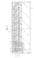
本実施の形態1の半導体装置は、たとえばBGA型の半導体装置であり、図1は、本実施の形態1の半導体装置に含まれるチップ1のレイアウトを説明する平面図である。また、図2は図1中の領域A1を拡大して示す要部平面図であり、図3および図4は図2中のA−A線に沿った断面を示し、図5および図6は図2中のB−B線に沿った断面を示し、図7および図8は図2中のC−C線に沿った断面を示し、図9および図10は図2中のD−D線に沿った断面を示している。また、図3および図4は外部接続用電極(バンプ電極あるいはボンディングワイヤ接続用のボンディングパッド)と信号用配線との接続状態を示し、図5〜図10は外部接続用電極と電源・GND(基準電位)用配線との接続状態を示し、図3〜図10中の太線矢印は電流経路を示している。図11は、図1中の領域A2にて形成された配線のレイアウト(平面)を示している。
(Embodiment 1)
The semiconductor device according to the first embodiment is, for example, a BGA type semiconductor device, and FIG. 1 is a plan view for explaining the layout of the
図1〜図11に示すように、チップ1においては、たとえば単結晶シリコンからなる半導体基板2の主面上にMISFET(Metal Insulator Semiconductor Field Effect Transistor)等の半導体素子3およびその半導体素子3と電気的に接続する配線4〜7等が設けられている。配線4〜6は、たとえば酸化シリコン等からなる層間絶縁膜8〜10に形成した配線形成用の溝に銅または銅合金を埋め込むことで形成されている。また、配線4の上層に形成された配線5および配線5の上層に形成された配線6が形成された溝については、底部に下層の配線との接続用の孔が設けられており、これら溝および孔を一括して銅または銅合金を埋め込むことで、下層の配線との接続用のプラグと配線とが一体に形成された構造となっている。なお、配線4〜6が形成された溝および孔の側壁および底面には、配線4〜6を形成する銅の層間絶縁膜8〜10等への拡散を防ぐために、チタン、窒化チタン、タンタルまたは窒化タンタル等の単層膜またはこれらの積層膜がバリア絶縁膜として形成されているが、図3〜図10中での図示は省略している。最上層の配線(第1配線)7は、たとえばアルミニウム膜またはアルミニウム合金膜を主導電層とする配線で、半導体基板2上に成膜されたアルミニウム膜またはアルミニウム合金膜をエッチングでパターニングすることで形成されている。配線7上には、たとえば酸化シリコン等の絶縁膜(保護膜)11および窒化シリコン膜等の絶縁膜からなる表面保護膜(保護膜)12が形成されている。また、本実施の形態1では、保護膜として酸化シリコン膜と窒化シリコン膜との積層膜を例示するが、これに限られるものではなく、たとえば窒化シリコン膜12等、単層の絶縁膜のみで形成することも可能である。
As shown in FIGS. 1 to 11, in a
また、上記の絶縁膜11および絶縁膜12の一部は開口されており、上記の配線7が露出している領域となっている。
In addition, a part of the insulating
上記配線7の一部は、上記開口部から露出された領域となっている。この配線7が露出した領域は、バンプ電極13が接続されるバンプ接続部(第2パッド)15、ボンディングワイヤ14が接続されるボンディングパッド(第1パッド)16および検査用探針が接触するテスト用パッド17となるための領域であり、その平面形状が他の配線7の領域と比較して、幅広に形成されている。
A part of the
最上層の配線7は、下層の配線4、5、6との電気的接続をチップ1の外周に沿って配置された入出力回路形成領域(第1回路領域)AIOにて行い、入出力回路形成領域AIOから相対的にチップ1の平面内側の領域(第2回路領域)へ延在している。また、ボンディングパッド16およびテスト用パッド17は、平面ではその入出力回路形成領域AIOに配置されている。
The
図3および図4に示すように、信号用配線となる配線7は、入出力回路形成領域AIOにて下層の配線4、5、6と電気的に接続し、入出力回路形成領域AIOに形成された入出力回路(半導体素子3を含む)および配線4を経由して、チップ1の内部に形成されたロジック(デジタル系)回路に電気的に接続されている。
As shown in FIGS. 3 and 4, the
図5および図6に示すように、電源電位または基準電位と電気的に接続する電源・GND用配線となる配線7は、入出力回路形成領域AIOにて下層の配線4、5、6と電気的に接続し、配線4を経由して、チップ1の内部に形成されたロジック回路への給電を行っている。電源・GND用配線となる配線7が電気的に接続する電源・GND用の配線4、5、6は、同じ配線層において複数の配線が同じ方向に延在し、1つ上層または下層の同電位の複数の配線が平面で交差する方向に延在する構造(以降、メッシュ構造と記す)となっている。図5および図6では、配線7が入出力回路形成領域AIOにて、1つ下層の配線6と接続している例を図示しているが、入出力回路形成領域AIOに加えて、それ以外の個所でも配線7が配線6と接続する構造であってもよい。
As shown in FIG. 5 and FIG. 6, the
図7〜図11に示すように、本実施の形態1においては、電源・GND用配線となる配線7はスリット構造となっており、下層の配線6と接続されることにより、図11に示すメッシュ配線を形成している。なお、たとえば第1配線層を電源配線とし、第2配線層をGND配線とするような構成とすれば、単一の配線層でもメッシュ配線は構成できることは明らかである。入出力回路形成領域AIO以外の領域(たとえば領域A2)でも複数個所で下層の配線6に接続している。この領域(第2回路領域)A2においては、配線7の下層の配線層(第2配線層)に形成された配線(第3配線)4、5、6もメッシュ構造となっている。
As shown in FIGS. 7 to 11, in the first embodiment, the
このように、電源・GND用配線となる配線4、5、6、7は、メッシュ構造とし、複数個所で上層および下層の配線と接続する構造とすることにより、安定した給電を行うことが可能となる。また、領域A2内のメッシュ構造となっている配線7にもバンプ接続部(第3パッド)15を設けて、接続するバンプ電極13をさらに形成してもよい。
As described above, the power supply /
図2〜図10に示すように、本実施の形態1においては、バンプ電極13によりチップ1が外部との電気的接続を行う場合においても、ボンディングワイヤ14によりチップ1が外部との電気的接続を行う場合においても、1本の配線7には、バンプ接続部15およびボンディングパッド16の両方が形成されている。ただし、すべての配線7にバンプ接続部15およびボンディングパッド16が設けられているわけではなく、バンプ接続部15が設けられていないボンディングパッド16も存在している。
As shown in FIGS. 2 to 10, in the first embodiment, even when the
バンプ電極13によりチップ1が外部との電気的接続を行う場合には、バンプ電極13を形成する位置における絶縁膜11および表面保護膜12にバンプ接続部15に達する開口部18を形成し、ボンディングパッド16およびテスト用パッド17上は、絶縁膜11および表面保護膜12で覆ったままの状態とする。バンプ電極13の形成時にボンディングパッド16およびテスト用パッド17上を絶縁膜11および表面保護膜12で覆ったままの状態とするのは、バンプ電極13となるはんだのリフロー熱でボンディングパッド16およびテスト用パッド17が溶融してしまうのを防止するためである。
When the
一方、ボンディングワイヤ14によりチップ1が外部との電気的接続を行う場合には、ボンディングパッド16およびテスト用パッド17上の絶縁膜11および表面保護膜12にボンディングパッド16およびテスト用パッド17のそれぞれに達する開口部19、20を形成し、バンプ接続部15上は、絶縁膜11および表面保護膜12で覆ったままの状態とする。ボンディングワイヤ14接続時に、バンプ接続部15上を絶縁膜11および表面保護膜12で覆ったままの状態とするのは、バンプ接続部15から腐食が進行してしまうのを防ぐためである。
On the other hand, when the
なお、図3、図5、図7および図9では、実際には形成されていない開口部19、20のそれぞれの開口位置19A、20Aを図示し、図4、図6、図8および図10では、実際には形成されていない開口部18の開口位置18Aも図示している。
3, 5, 7, and 9, the opening positions 19 </ b> A and 20 </ b> A of the
上記のように、本実施の形態1によれば、バンプ電極13によりチップ1が外部との電気的接続を行う場合と、ボンディングワイヤ14によりチップ1が外部との電気的接続を行う場合とで、最上層の配線7を形成するまでのチップ1は、同じレイアウトとすることができる。それにより、バンプ電極13によりチップ1が外部との電気的接続を行う場合と、ボンディングワイヤ14によりチップ1が外部との電気的接続を行う場合とで、最上層の配線7を形成するまでは、同じマスクを用いてパターン形成することが可能となり、工程を共通化することが可能となる。その結果、本実施の形態1の半導体装置の量産性を向上でき、製造コストを低減することができる。
As described above, according to the first embodiment, when the
開口部18、19、20のレイアウト検証は、開口部18と開口部19、20とで別レイヤ(データタイプの切り替えとしてもよい)としておき、それぞれに適したレイアウト検証ルールを作成することで実施できる。なお、開口部18、19、20のレイアウト検証は、上記開口部のデータタイプ、またはレイヤをボンディングワイヤを使用する場合とバンプ電極を使用する場合とで別に持たせることにより、設計者が同一のルールファイルで開口部18、19、20のレイアウト検証ルールを使い分け、前記レイヤを選択して用いてもよい。
The layout verification of the
また、開口部18、19、20用のマスク作成は、マスク作成支持をするデータファイルであるMPD(Mask Pattern Data Specification)を用い、バンプ電極13を用いる場合には開口部18のレイヤをアサインし、ボンディングワイヤ14を用いる場合には開口部19、20のレイヤをアサインし、それぞれ専用のマスクを作成する。このようなウエハレベルでのプロセス方式とすることで、バンプ電極13を用いる場合とボンディングワイヤ14を用いる場合とで、チップ1の作り分けが可能となる。
The masks for the
なお、開口部18、19、20のパターン転写工程に関しては、マスクを作成せず、電子ビームによる直描方式としてもよい。それにより、マスク製造にかかるコストを削減することができる。また、配線7より下層の配線パターンについても、電子ビームによる直描方式としてもよい。
In addition, regarding the pattern transfer process of the
次に、本実施の形態1のチップ1の製造工程について、図12〜図15を用いて説明する。前述したように、バンプ電極13を用いる場合とボンディングワイヤ14を用いる場合とで、配線7を形成するまでの工程は同じである。
Next, the manufacturing process of the
まず、図12に示すように、集積回路を形成する半導体素子3および配線4〜6が形成された半導体基板2上に、たとえば酸化シリコン膜を堆積して層間絶縁膜10Aを形成する。
First, as shown in FIG. 12, an
続いて、フォトリソグラフィ技術によりパターニングされたフォトレジスト膜をマスクとして層間絶縁膜10Aをエッチングし、配線6に達するコンタクトホールを形成する。
Subsequently, the
次いで、そのコンタクトホール内を含む層間絶縁膜10A上に薄いチタン膜あるいは窒化チタン膜の単層膜、またはこれらの積層膜を堆積してバリア導電膜を形成した後、層間絶縁膜10A上にタングステン膜を堆積し、そのタングステン膜でコンタクトホールを埋め込む。次いで、コンタクトホール外のバリア導電膜およびタングステン膜を除去することにより、配線6と接続するプラグ7Aを形成する。
Next, a thin titanium film or a single layer film of titanium nitride film or a laminated film thereof is deposited on the
次に、図13に示すように、半導体基板2上に、チタン膜、アルミニウム膜(あるいはアルミニウム合金膜)および窒化チタン膜を順次堆積した後、フォトレジスト膜をマスクとしたドライエッチングによりそれらチタン膜、アルミニウム膜(あるいはアルミニウム合金膜)および窒化チタン膜をパターニングし、配線7を形成する。前述したように、この工程において、バンプ接続部15、ボンディングパッド16およびテスト用パッド17が形成および規定される。
Next, as shown in FIG. 13, a titanium film, an aluminum film (or an aluminum alloy film), and a titanium nitride film are sequentially deposited on the
続いて、半導体基板1上に、酸化シリコン膜および窒化シリコン膜を順次堆積し、絶縁膜11および表面保護膜12を形成する。
Subsequently, a silicon oxide film and a silicon nitride film are sequentially deposited on the
以降の工程は、バンプ電極13を用いる場合とボンディングワイヤ14を用いる場合とで異なってくる。
The subsequent steps differ depending on whether the
バンプ電極13を用いる場合には、図14に示すように、フォトリソグラフィ技術によりパターニングされたフォトレジスト膜をマスクとして表面保護膜12および絶縁膜11をエッチングし、配線7に達する開口部18を形成する。続いて、たとえば無電解めっき法により開口部18下の配線7上に金膜等の導電性膜を成膜し、バンプ電極用下地膜13Aを形成する。
When the
次に、バンプ電極13を形成する。バンプ電極13の製造工程としては、たとえば、はんだ印刷技術により半導体基板2上にはんだペーストを印刷した後、リフロー処理によりはんだペーストを溶融および再結晶化させ、バンプ電極用下地膜13A上にバンプ電極13を形成する(図3、図5、図7および図9参照)。そのはんだペーストとしては、たとえば錫、銀および銅から形成された鉛フリーはんだを用いることができる。また、はんだペーストを用いる代わりに、予め球状に成形されたはんだボールを開口部18上に供給した後に、半導体基板2に対してリフロー処理を施すことによってもバンプ電極13を形成することができる。
Next, the
その後、ウエハ状態の半導体基板2を区画されたチップ領域間のスクライブ(ダイシング)領域に沿って切断し、個々のチップ1に分割する。分割されたチップ1は、実装基板上にバンプ電極13を介して実装することができる。チップ1を実装基板上に配置した後、バンプ電極13をリフローし、次いでチップ1と実装基板との間にアンダーフィル樹脂を充填し、本実施の形態1の半導体装置を製造する。
Thereafter, the
ボンディングワイヤ14を用いる場合には、図15に示すように、フォトリソグラフィ技術によりパターニングされたフォトレジスト膜をマスクとして表面保護膜12および絶縁膜11をエッチングし、入出力回路形成領域AIOにて配線7に達する開口部19、20を形成する。
When the
次に、テスト用パッド17にプローブによるウエハテストを行う。プローブによるテストでは、プローブの針を直接テスト用パッド17に接触させることで行われる。もし、実際にボンディングワイヤ14を形成するためのボンディングパッド16でテストを行えば、プローブ針による応力からボンディングパッド16下の層間絶縁膜にクラックが発生する等の不具合が生じることが懸念される。従って、本実施の形態1では、プローブによるテスト用のテスト用パッド17の領域と、実際にボンディングワイヤ14を形成するためのボンディングパッド16の領域とを別々に形成している。
Next, a wafer test using a probe is performed on the
次に、ウエハ状態の半導体基板2を区画されたチップ領域間のスクライブ(ダイシング)領域(分割領域)に沿って切断し、個々のチップ1に分割する。分割したチップ1は、DAF(Die Attached Film)等を用いて実装基板(たとえば多層配線基板)に搭載する。次いで、開口部19A下のボンディングパッド16と実装基板の電極とをボンディングワイヤ14で接続した後(図4、図6、図8および図10参照)、モールド樹脂によりチップ1およびボンディングワイヤ14を封止する。その後、モールド樹脂および実装基板を所定位置で切断し、本実施の形態1の半導体装置を製造する。
Next, the
ここで、図16および図17は、チップ1におけるバンプ接続部15(もしくはバンプ電極13)、ボンディングパッド16およびテスト用パッド17付近の要部平面図であり、図16はボンディングワイヤ14を用いた場合の平面を示し、図17はバンプ電極13を用いた場合を示している。前述したように、ボンディングパッド16およびテスト用パッド17は、入出力回路形成領域AIOに配置されており、ボンディングパッド16およびテスト用パッド17下には、入出力回路を含む入出力回路セルIOCが形成されている。
Here, FIGS. 16 and 17 are plan views of the main parts in the vicinity of the bump connecting portion 15 (or bump electrode 13),
このように、ここまでの本実施の形態1では、ボンディングパッド16およびテスト用パッド17を個々に配置する場合について説明したが、図18および図19に示すように、ボンディングパッド16とテスト用パッド17とが一体に形成された平面サイズの大きな構造、もしくはテスト用パッド17そのものを省略した構造としてもよい。
As described above, in the first embodiment so far, the case where the
また、最上層の配線7に関してはアルミニウムを主成分とした構成で説明したが、銅等の他の材質であっても同様の効果が得られることは明らかである。また、最上層の配線7のみをアルミニウムで形成し、それより下層の配線層は銅を主体とする配線層で形成してもよい。層間絶縁膜10に配線6を形成する場合について例示すると、層間絶縁膜10を形成した後に、下層の配線5に接続する孔を形成し、その後、配線6を構成する配線溝を形成する。次に、孔および溝内に、タンタルや窒化タンタル等の導電性膜からなるバリアメタル膜を形成し、そのバリアメタル膜上に銅を主成分とする導電性膜(銅膜)を形成する。そして、溝外部のバリアメタル膜および銅膜を、CMP法等によって除去することで、孔および溝内にバリアメタル膜および銅膜を埋め込み、配線6、および配線6と配線5とを接続する接続部を形成することができる。
Further, although the
ところで、本実施の形態1において、チップ1を外部のたとえばメモリ回路等の他のチップと電気的に接続させる場合には、ボンディングワイヤ14を用いる構造とし、たとえば領域A3(図1参照)に配置されたボンディングパッド16(配線7)がメモリ回路と電気的に接続するためのインターフェースとなる構成とする。一方、チップ1を外部のメモリ回路と電気的に接続させる必要がない場合には、バンプ電極13を用いる構造とし、たとえば領域A3にて外部のメモリ回路と電気的に接続させるために設けた配線7上でのバンプ電極13の形成は省略することで、チップ1のサイズを縮小化することができる。そのため、外部のメモリ回路と電気的に接続するためのインターフェースとなる領域A3においては、たとえばボンディングパッド16は51個となり、バンプ電極13は10個となる。すなわち、本実施の形態1において、チップ1に形成されるボンディングパッド16の数は、バンプ接続部15の数よりも多い。
In the first embodiment, when the
なお、バンプ電極13を用いる構成となった場合には、メモリ回路と電気的に接続するためのインターフェースとなる領域A3の配線7が開放端となるが、そのような配線7については、プルアップもしくはプルダウン等の処理を施し、開放端となってもチップ1内に形成されたロジック回路の動作に支障を来たさないように設計する必要がある。
In the case where the
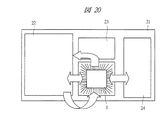
図20〜図23は、本実施の形態1のチップ1を無線システムのコントローラとしてモジュール基板21に実装した場合の例を示したものであり、図20および図21は、それぞれ上記ボンディングワイヤ14を用いている場合の平面図および側面図であり、図22および図23は、それぞれ上記バンプ電極13を用いている場合の平面図および側面図である。モジュール基板21には、チップ1以外に、高周波動作を行うRF(Radio Frequency)回路が形成されたRFチップ22およびバイパスコンデンサチップ23等も実装されている。バイパスコンデンサチップ23は、電源安定化のために電源ラインに電気的に挿入されている。また、図20〜図23中の矢印は、各チップ間の信号の流れを示すものである。
20 to 23 show an example in which the
前述したように、ボンディングワイヤ14が用いられたチップ1をモジュール基板21に実装した場合には、メモリ回路が形成されたメモリチップ24もモジュール基板21に実装することができる(図20および図21参照)。それにより、ファームウエア等のプログラムを多数搭載することが可能となるため、無線システム全体の機能を向上させることが可能となる。
As described above, when the
一方、バンプ電極13が用いられたチップ1を実装した場合には、メモリチップ24は実装されない構成となるため、最小構成で無線システムを構築することが可能となる(図22および図23参照)。それにより、その無線システムが構築されたモジュールのサイズを最小化することができるようになるので、たとえば携帯電話のようなモジュールの実装領域が限定されるような機器に対しても、無線システムを適用することが可能となる。
On the other hand, when the
(実施の形態2)
図24は、本実施の形態2のチップ1の要部平面図であり、前記実施の形態1で示した図1中の領域A4に相当する領域を図示したものである。
(Embodiment 2)
FIG. 24 is a plan view of a main part of the
図24に示すように、相対的にチップ1の外周1Aに近くその外周1Aに沿った領域A4には、入出力回路セルIOCが形成され、その入出力回路セルIOC上には前記実施の形態1でも説明したボンディングパッド16およびテスト用パッド17が形成されている。
As shown in FIG. 24, an input / output circuit cell IOC is formed in a region A4 relatively close to the
図2に示されるように、前記実施の形態1でも説明したように、1本の配線7にバンプ接続部15、ボンディングパッド16およびテスト用パッド17も形成されている。入出力回路セルIOC上にはボンディングパッド16およびテスト用パッド17が形成されていることから、配線7をバンプ電極13が平面で入出力回路セルIOCと重ならない領域、たとえば相対的にチップ1の中心方向まで引き回してバンプ接続部15を配置している。
As shown in FIG. 2, as described in the first embodiment, the
ここで、図24に示すように、領域A4において、隣接する2つの入出力回路セルIOC間にバンプ電極13を配置できるスペースを確保できるように入出力回路セルIOCの配置レイアウトを設計できる場合には、そのような入出力回路セルIOCの配置レイアウトとし、入出力回路セルIOC間のスペースへ配線7を引き回してバンプ接続部15およびバンプ電極13を配置する。それにより、相対的にチップ1の中心方向でバンプ電極13を配置するための領域を確保する必要がなくなるので、チップ1の面積を縮小し、チップ1を小型化することが可能となる。特に、このような領域A4は、図1に示すアナログ系回路領域A6に近い場合に、有効に活用することができる。その理由は、アナログ系回路領域A6は、他のロジック系回路が形成されるような領域と比較して、信号線や電源線を引き込む割合が少ないので、入出力回路セルIOCの数が少なく済むからである。
Here, as shown in FIG. 24, when the layout of the input / output circuit cells IOC can be designed so as to secure a space in which the
なお、領域A3のような他の領域においても、入出力回路セルIOCの数が少なく済む場合には、隣接する2つの入出力回路セルIOC間にバンプ電極13を配置することができる。
In other regions such as the region A3, when the number of input / output circuit cells IOC is small, the
また、図25に示すように、入出力回路セルIOC間のスペースに配置されたバンプ電極13下を有効的に活用するために、入出力回路セルIOC間のスペースに配置されたバンプ電極13下に、たとえば通常のロジック(デジタル系)回路や、静電気放電(Electrostatic Discharge;ESD)対策用のダイオードを含む保護回路を形成してもよい。それにより、チップ1に更なる回路機能を搭載したり、チップ1の面積を更に縮小してチップ1を更に小型化したりすることが可能となる。
Further, as shown in FIG. 25, in order to effectively utilize the bottom of the
また、相対的にチップ1の外周1Aに近くその外周1Aに沿った領域A5(図1参照)においても、上記の領域A4と同様のレイアウトで入出力回路セルIOCを配置し、入出力回路セルIOC間のスペースへ配線7を引き回してバンプ接続部15およびバンプ電極13を配置する。
Also in the region A5 (see FIG. 1) that is relatively close to the
ところで、本実施の形態2において、その領域A5は、チップ1の外周1Aと、設計上バンプ電極13を配置することができない領域(第3回路領域)A6との間の狭い領域であり、さらにチップ1の外周1Aから所定距離T1以上を離間してバンプ電極13を配置しなければならない、バンプ電極13の配置に当たって制約のある領域である。なお、その領域A6は、相対的に領域A5よりチップ1の内側に位置し、たとえばアナログ系回路が形成されている。仮に、アナログ系回路領域A6上に配線7や、バンプ電極13を形成すると、配線7からのノイズや寄生容量が発生する虞がある。アナログ系回路領域A6は、他のロジック回路に比べて、ノイズや寄生容量に敏感な領域のため、上記のような制約が特に厳しい領域となっている。
By the way, in the second embodiment, the area A5 is a narrow area between the
図26に示すように、このような領域A5において、相対的にチップ1の外周1Aに近い位置に配置されたバンプ電極13と、相対的に領域A6に近い位置に配置されたバンプ電極13とを、チップ1の外周1Aと直行するような方向でピッチP1で並べた場合には、このピッチP1が相対的にチップ1の外周1Aに近い位置に配置されたバンプ電極13の配置ピッチP2と同じであっても、相対的に領域A6に近い位置に配置されたバンプ電極13がバンプ電極13を配置することができない領域A6に入ってしまう虞がある。
As shown in FIG. 26, in such a region A5, the
また、図27に示すように、相対的にチップ1の外周1Aに近い位置に配置されたバンプ電極13の2つ(もしくは1つ)と、相対的に領域A6に近い位置に配置されたバンプ電極13の1つ(もしくは2つ)とを、二等辺三角形の頂点となるように配置して、バンプ電極13が領域A6と重ならないようにした場合には、チップ1の外周1Aに沿った方向でのバンプ電極13の配置ピッチP2が広がってしまい、所望の数のバンプ電極13を配置しようとすると、チップ1の大型化を招く虞がある。なお、図27中では、相対的にチップ1の外周1Aに近い位置に配置されたバンプ電極13と、隣接する相対的に領域A6に近い位置に配置されたバンプ電極13とのピッチをP1としている。
In addition, as shown in FIG. 27, two (or one) of the
そこで、本実施の形態2では、図28に示すように、相対的にチップ1の外周1Aに近い位置に配置されたバンプ電極13の2つ(もしくは1つ)と、相対的に領域A6に近い位置に配置されたバンプ電極13の1つ(もしくは2つ)とを、正三角形の頂点となるように配置する。すなわち、各バンプ電極13の中心を頂点として、各頂点を結んだ形が、正三角形になるように配置している。それにより、図27に示したような二等辺三角形の頂点となるようなバンプ電極13の配置方法に比べて、小さい領域で所望の数のバンプ電極13を配置することが可能となる。それにより、チップ1のサイズが大きくなってしまうことを防ぎ、チップ1のサイズを維持もしくは縮小することが可能となる。
Therefore, in the second embodiment, as shown in FIG. 28, two (or one)
以上、本発明者によってなされた発明を実施の形態に基づき具体的に説明したが、本発明は前記実施の形態に限定されるものではなく、その要旨を逸脱しない範囲で種々変更可能であることはいうまでもない。 As mentioned above, the invention made by the present inventor has been specifically described based on the embodiment. However, the present invention is not limited to the embodiment, and various modifications can be made without departing from the scope of the invention. Needless to say.
本発明の半導体装置の製造方法および半導体装置は、チップがボンディングワイヤまたはバンプ電極を介して実装された構造を有する半導体装置に広く適用することができる。 The method for manufacturing a semiconductor device and the semiconductor device of the present invention can be widely applied to semiconductor devices having a structure in which a chip is mounted via bonding wires or bump electrodes.
1 チップ
1A 外周
2 半導体基板
3 半導体素子
4〜6 配線(第3配線)
7 配線(第1配線、第2配線)
7A プラグ
8〜10、10A 層間絶縁膜
11 絶縁膜(保護膜)
12 表面保護膜(保護膜)
13 バンプ電極
13A バンプ電極用下地膜
14 ボンディングワイヤ
15 バンプ接続部(第2パッド、第3パッド)
16 ボンディングパッド(第1パッド)
17 テスト用パッド
18 開口部
18A 開口位置
19 開口部
19A 開口位置
20 開口部
20A 開口位置
21 モジュール基板
22 RFチップ
23 バイパスコンデンサチップ
24 メモリチップ
A1 領域
A2 領域(第2回路領域)
A3 領域
A4 領域
A5 領域
A6 領域(第3回路領域)
AIO 入出力回路形成領域(第1回路領域)
IOC 入出力回路セル
LEC 回路セル
1
7 Wiring (first wiring, second wiring)
7A plug 8-10, 10A
12 Surface protective film (protective film)
13
16 Bonding pad (first pad)
17
A3 area A4 area A5 area A6 area (third circuit area)
AIO I / O circuit formation area (first circuit area)
IOC I / O circuit cell LEC circuit cell
Claims (17)
(b)前記複数のチップ領域の各々内にて、第1回路領域から第2回路領域に延在し、前記集積回路と電気的に接続する第1配線を前記集積回路の上層に形成する工程、
(c)前記第1回路領域の前記第1配線の一部を第1パッドと規定し、前記第2回路領域の前記第1配線の一部を第2パッドと規定する工程、
(d)前記第1配線の存在下で前記半導体基板上に保護膜を形成する工程、
(e)前記第1パッド上または前記第2パッド上の前記保護膜に開口部を形成する工程、
(f)前記分割領域に沿って前記半導体基板を切断し、個々の半導体チップに分割する工程、
(g)前記半導体チップを実装基板に実装し、ボンディングワイヤまたはバンプ電極を介して前記半導体チップと前記実装基板とを電気的に接続する工程、
を含み、
前記(g)工程において、前記ボンディングワイヤを介して前記半導体チップと前記実装基板とを電気的に接続する場合には、前記(e)工程において前記開口部は前記第1パッド上の前記保護膜に形成し、且つ、前記第2パッド上は前記保護膜で覆われた状態として、前記(g)工程において前記ボンディングワイヤを前記開口部下にて前記第1パッドに直接接続し、
前記(g)工程において、前記バンプ電極を介して前記半導体チップと前記実装基板とを電気的に接続する場合には、前記(e)工程において、前記開口部は前記第2パッド上の前記保護膜に形成し、且つ、前記第1パッド上は前記保護膜で覆われた状態として、前記開口部下にて前記第2パッドと接続する前記バンプ電極を前記第2パッド上に直接形成することを特徴とする半導体装置の製造方法。 (A) forming an integrated circuit in each of the plurality of chip regions on a semiconductor substrate partitioned into a plurality of chip regions by divided regions;
(B) forming a first wiring extending from the first circuit region to the second circuit region in each of the plurality of chip regions and electrically connected to the integrated circuit in an upper layer of the integrated circuit; ,
(C) defining a part of the first wiring in the first circuit region as a first pad and defining a part of the first wiring in the second circuit region as a second pad;
(D) forming a protective film on the semiconductor substrate in the presence of the first wiring;
(E) forming an opening in the protective film on the first pad or the second pad;
(F) cutting the semiconductor substrate along the divided region and dividing it into individual semiconductor chips;
(G) step of the mounting a semiconductor chip on a mounting board, for electrically connecting the mounting substrate and the semiconductor chip through a bonding wire or bump electrodes,
Including
Wherein in step (g), when connecting the bonding wires and the semiconductor chip through said mounting board electrically, the (e) the opening in the process the protection on the first pad Forming the film, and the second pad is covered with the protective film, and in the step (g), the bonding wire is directly connected to the first pad under the opening,
Wherein in step (g), when said via bump electrodes to electrically connect the mounting board and the semiconductor chip, in step (e), said opening the on the second pad Forming the bump electrode directly on the second pad to be connected to the second pad under the opening with the protective film formed on the first pad and covered with the protective film A method of manufacturing a semiconductor device.
前記第1配線は電源電位または基準電位と電気的に接続し、
前記半導体チップは、前記バンプ電極を介して前記実装基板と電気的に接続し、
前記(b)工程では、前記第1配線が形成された第1配線層において、前記第1配線と電気的に接続し、互いに平行に延在する複数の第2配線を形成し、
前記(c)工程では、前記第2配線の一部を第3パッドと規定し、
前記(e)工程では、前記第3パッド上の前記保護膜に前記開口部を形成し、さらに前記開口部下にて前記第3パッドと接続する前記バンプ電極を前記第3パッド上に直接形成することを特徴とする半導体装置の製造方法。 In the manufacturing method of the semiconductor device according to claim 1,
The first wiring is electrically connected to a power supply potential or a reference potential,
The semiconductor chip is electrically connected with the mounting substrate via the bump electrode,
Wherein in the step (b), the first wiring layer in which the first wiring is formed, said connecting first wiring electrically, to form a multiple second wiring that Mashimasu extending parallel to each other,
In the step (c), a part of the second wiring is defined as a third pad,
In the step (e), the opening is formed in the protective film on the third pad, and the bump electrode connected to the third pad is directly formed on the third pad below the opening. A method for manufacturing a semiconductor device.
前記(a)工程では、前記第1配線および前記第2配線と電気的に接続し、互いに平行に延在する複数の第3配線を前記第1配線層より下層の第2配線層にて形成し、
前記複数の第2配線および前記複数の第3配線は、前記半導体チップの中央を含む前記第2回路領域に形成することを特徴とする半導体装置の製造方法。 The method of manufacturing a semiconductor device according to claim 2.
In the step (a), a plurality of third wirings that are electrically connected to the first wiring and the second wiring and extend in parallel to each other are formed in a second wiring layer below the first wiring layer. And
The method for manufacturing a semiconductor device, wherein the plurality of second wirings and the plurality of third wirings are formed in the second circuit region including a center of the semiconductor chip.
前記半導体チップは、前記バンプ電極を介して前記実装基板と電気的に接続し、
前記半導体チップ内にて、前記第2回路領域を、相対的に前記半導体チップの外周に近い前記第1回路領域と、前記第1回路領域および前記第2回路領域よりも前記半導体チップの内側の第3回路領域との間に配置することを特徴とする半導体装置の製造方法。 In the manufacturing method of the semiconductor device according to claim 1,
The semiconductor chip is electrically connected with the mounting substrate via the bump electrode,
Within the semiconductor chip, the second circuit region is relatively closer to the outer periphery of the semiconductor chip, and the inner side of the semiconductor chip than the first circuit region and the second circuit region. A method of manufacturing a semiconductor device, wherein the semiconductor device is disposed between the third circuit region and the third circuit region.
前記半導体チップは、前記バンプ電極を介して前記実装基板と電気的に接続し、
入出力回路を含む前記第1回路領域を、前記半導体チップの外周に沿って複数配置し、
前記第2回路領域を、前記第1回路領域間に配置することを特徴とする半導体装置の製造方法。 In the manufacturing method of the semiconductor device according to claim 1,
The semiconductor chip is electrically connected with the mounting substrate via the bump electrode,
A plurality of the first circuit regions including input / output circuits are arranged along the outer periphery of the semiconductor chip,
A method of manufacturing a semiconductor device, wherein the second circuit region is disposed between the first circuit regions.
前記バンプ電極下の前記第2回路領域にデジタル系回路またはESD対策用の半導体素子を含む第1回路を形成することを特徴とする半導体装置の製造方法。 In the manufacturing method of the semiconductor device according to claim 5,
A method for manufacturing a semiconductor device, comprising: forming a first circuit including a digital circuit or an ESD countermeasure semiconductor element in the second circuit region under the bump electrode.
前記第2回路領域を、前記第1回路領域と、前記第1回路領域および前記第2回路領域よりも前記半導体チップの中心に近い第3回路領域との間に配置し、
前記バンプ電極のうち、前記第1回路領域間の前記第2回路領域上の1つまたは隣り合う2つの前記バンプ電極と、前記第1回路領域と前記第3回路領域との間の前記第2回路領域上の1つまたは隣り合う2つの前記バンプ電極とが、正三角形の各頂点となるように前記バンプ電極を配置することを特徴とする半導体装置の製造方法。 In the manufacturing method of the semiconductor device according to claim 5,
The second circuit region is disposed between the first circuit region and the third circuit region closer to the center of the semiconductor chip than the first circuit region and the second circuit region;
Among the bump electrodes, one or two adjacent bump electrodes on the second circuit region between the first circuit regions, and the second between the first circuit region and the third circuit region. A method of manufacturing a semiconductor device, wherein the bump electrodes are arranged so that one or two adjacent bump electrodes on a circuit region are the vertices of an equilateral triangle.
前記第1パッドの数は、前記第2パッドの数よりも多いことを特徴とする半導体装置の製造方法。 In the manufacturing method of the semiconductor device according to claim 1,
The method of manufacturing a semiconductor device, wherein the number of the first pads is larger than the number of the second pads.
前記(b)工程において、前記第1配線は複数形成し、
前記複数の前記第1配線の一部は、メモリチップとの間のインターフェースとなり、
前記実装基板に前記メモリチップを実装する場合には、前記(g)工程において、前記ボンディングワイヤを介して前記半導体チップと前記実装基板とを電気的に接続し、前記インターフェースと前記メモリチップとを電気的に接続し、
前記実装基板に前記メモリチップを実装しない場合には、前記(g)工程において、前記バンプ電極を介して前記半導体チップと前記実装基板とを電気的に接続し、前記(c)工程において、前記インターフェースには前記第2パッドを規定せず、前記(e)工程では前記インターフェースと接続する前記バンプ電極は形成しないことを特徴とする半導体装置の製造方法。 In the manufacturing method of the semiconductor device of Claim 8,
In the step (b), a plurality of the first wirings are formed,
Some of the plurality of first wirings serve as interfaces with the memory chip,
When implementing the memory chip to the mounting substrate, in step (g), said via a bonding wire electrically connecting the mounting substrate and the semiconductor chip, and said interface and said memory chip Electrically connect
If you do not implement the memory chip to the mounting substrate, in step (g), in the via bump electrodes to electrically connect the mounting board and the semiconductor chip, the step (c), The method of manufacturing a semiconductor device, wherein the second pad is not defined in the interface, and the bump electrode connected to the interface is not formed in the step (e).
前記ボンディングワイヤを介して前記半導体チップと前記実装基板とを電気的に接続する場合と、前記バンプ電極を介して前記半導体チップと前記実装基板とを電気的に接続する場合とで、前記第1回路領域、前記第2回路領域、前記集積回路および前記第1配線は、同じレイアウトで形成することを特徴とする半導体装置の製造方法。 In the manufacturing method of the semiconductor device according to claim 1,
Wherein the case via a bonding wire electrically connects the mounting substrate and the semiconductor chip, in the case of electrically connecting the mounting substrate and the semiconductor chip through the bump electrode, the The method of manufacturing a semiconductor device, wherein the first circuit region, the second circuit region, the integrated circuit, and the first wiring are formed with the same layout.
(b)前記第1配線上に、第1絶縁膜を形成する工程、
(c)前記第1絶縁膜に開口部を形成し、前記第1配線の一部を露出させる工程、
を有する半導体装置の製造方法であって、
前記(a)工程で、前記第1配線には、ボンディングワイヤが直接接続されるための複数の第1領域と、バンプ電極が直接形成されるための複数の第2領域とが形成されており、
前記(c)工程で、前記半導体装置に前記ボンディングワイヤを使用する場合には、前記開口部は前記複数の第1領域にそれぞれ形成され、且つ、前記複数の第2領域には形成されず、
前記(c)工程で、前記半導体装置に前記バンプ電極を使用する場合には、前記開口部は前記複数の第2領域にそれぞれ形成され、かつ、前記複数の第1領域には形成されないことを特徴とする半導体装置の製造方法。 (A) forming a first wiring on the semiconductor substrate;
(B) forming a first insulating film on the first wiring;
(C) forming an opening in the first insulating film and exposing a part of the first wiring;
A method of manufacturing a semiconductor device having
In the step (a), a plurality of first regions for directly connecting bonding wires and a plurality of second regions for directly forming bump electrodes are formed in the first wiring. ,
In the step (c), when the bonding wire is used for the semiconductor device, the openings are formed in the plurality of first regions, respectively, and are not formed in the plurality of second regions,
In the step (c), when the bump electrode is used in the semiconductor device, the opening is formed in each of the plurality of second regions and is not formed in the plurality of first regions. A method of manufacturing a semiconductor device.
前記複数の第1領域の数は、前記複数の第2領域の数よりも多いことを特徴とする半導体装置の製造方法。 The method of manufacturing a semiconductor device according to claim 11 .
The method of manufacturing a semiconductor device, wherein the number of the plurality of first regions is larger than the number of the plurality of second regions.
前記複数の第1領域の下には、入出力回路用セルがそれぞれ形成されていることを特徴とする半導体装置の製造方法。 The method of manufacturing a semiconductor device according to claim 11 .
An input / output circuit cell is formed below each of the plurality of first regions.
前記複数の第2領域のうちの一部は、隣接する入出力回路用セルの間に形成されていることを特徴とする半導体装置の製造方法。 14. The method of manufacturing a semiconductor device according to claim 13 ,
A part of said 2nd area | region is formed between the cells for adjacent input / output circuits, The manufacturing method of the semiconductor device characterized by the above-mentioned.
前記隣接する入出力回路用セルの間に形成されている前記第2領域の下の前記半導体基板には、デジタル系回路またはESD対策用の半導体素子が形成されていることを特徴とする半導体装置の製造方法。 15. The method of manufacturing a semiconductor device according to claim 14 ,
A semiconductor device having a digital circuit or an ESD countermeasure semiconductor element formed on the semiconductor substrate under the second region formed between the adjacent input / output circuit cells. Manufacturing method.
前記バンプ電極は、バンプ電極用下地膜と、前記バンプ電極用下地膜の上に形成されたペーストを含むことを特徴とする半導体装置の製造方法。The method for manufacturing a semiconductor device, wherein the bump electrode includes a bump electrode base film and a paste formed on the bump electrode base film.
前記バンプ電極用下地膜は金からなり、The base film for the bump electrode is made of gold,
前記ペーストは錫、銀および銅からなることを特徴とする半導体装置の製造方法。The method of manufacturing a semiconductor device, wherein the paste is made of tin, silver, and copper.
Priority Applications (6)
| Application Number | Priority Date | Filing Date | Title |
|---|---|---|---|
| JP2008042695A JP5342154B2 (en) | 2008-02-25 | 2008-02-25 | Manufacturing method of semiconductor device |
| TW097144917A TWI459483B (en) | 2008-02-25 | 2008-11-20 | Manufacturing method of semiconductor device |
| KR1020080124766A KR101566026B1 (en) | 2008-02-25 | 2008-12-09 | A semiconductor device and a method of manufacturing the same |
| CN2008101865713A CN101521169B (en) | 2008-02-25 | 2008-12-25 | Semiconductor device and a method of manufacturing the same |
| US12/367,297 US8222082B2 (en) | 2008-02-25 | 2009-02-06 | Semiconductor device and a method of manufacturing the same |
| US13/306,659 US8384185B2 (en) | 2008-02-25 | 2011-11-29 | Semiconductor device and a method of manufacturing the same |
Applications Claiming Priority (1)
| Application Number | Priority Date | Filing Date | Title |
|---|---|---|---|
| JP2008042695A JP5342154B2 (en) | 2008-02-25 | 2008-02-25 | Manufacturing method of semiconductor device |
Publications (2)
| Publication Number | Publication Date |
|---|---|
| JP2009200394A JP2009200394A (en) | 2009-09-03 |
| JP5342154B2 true JP5342154B2 (en) | 2013-11-13 |
Family
ID=40997501
Family Applications (1)
| Application Number | Title | Priority Date | Filing Date |
|---|---|---|---|
| JP2008042695A Expired - Fee Related JP5342154B2 (en) | 2008-02-25 | 2008-02-25 | Manufacturing method of semiconductor device |
Country Status (5)
| Country | Link |
|---|---|
| US (2) | US8222082B2 (en) |
| JP (1) | JP5342154B2 (en) |
| KR (1) | KR101566026B1 (en) |
| CN (1) | CN101521169B (en) |
| TW (1) | TWI459483B (en) |
Families Citing this family (22)
| Publication number | Priority date | Publication date | Assignee | Title |
|---|---|---|---|---|
| JP5609144B2 (en) * | 2010-02-19 | 2014-10-22 | ソニー株式会社 | Semiconductor device and through electrode test method |
| JP5355499B2 (en) * | 2010-06-03 | 2013-11-27 | 株式会社東芝 | Semiconductor device |
| DE102011107349B4 (en) * | 2010-06-30 | 2016-05-12 | Micronas Gmbh | Bond pad on a semiconductor substrate |
| JP5729126B2 (en) * | 2011-05-18 | 2015-06-03 | 株式会社デンソー | Manufacturing method of semiconductor device |
| US9064707B2 (en) | 2011-09-14 | 2015-06-23 | Micronas Gmbh | Bonding contact area on a semiconductor substrate |
| CN103620771B (en) | 2011-11-10 | 2016-11-16 | 松下电器产业株式会社 | Semiconductor device |
| US8953336B2 (en) * | 2012-03-06 | 2015-02-10 | Taiwan Semiconductor Manufacturing Co., Ltd. | Surface metal wiring structure for an IC substrate |
| JP2013229455A (en) * | 2012-04-26 | 2013-11-07 | Renesas Electronics Corp | Semiconductor device and method for manufacturing the same |
| TWI483378B (en) * | 2013-01-04 | 2015-05-01 | Tsai Yu Huang | Three dimensional stacked structure for chips |
| JP2015079848A (en) * | 2013-10-17 | 2015-04-23 | シナプティクス・ディスプレイ・デバイス株式会社 | Semiconductor integrated circuit device for driving display device |
| JP2015109408A (en) * | 2013-10-22 | 2015-06-11 | マイクロン テクノロジー, インク. | Composite chip, semiconductor device, and manufacturing method of semiconductor device |
| KR20160056379A (en) | 2014-11-10 | 2016-05-20 | 삼성전자주식회사 | Chip using triple pad configuration and packaging method thereof |
| CN105720910A (en) * | 2014-12-01 | 2016-06-29 | 中电电气(上海)太阳能科技有限公司 | Junction box for solar cell module |
| JP6565238B2 (en) * | 2015-03-17 | 2019-08-28 | セイコーエプソン株式会社 | Liquid jet head |
| KR102387541B1 (en) | 2015-03-25 | 2022-04-18 | 삼성전자주식회사 | Semiconductor chip, and flip chip package and wafer level package including the same |
| WO2016166890A1 (en) * | 2015-04-17 | 2016-10-20 | オリンパス株式会社 | Imaging device |
| JP2017045900A (en) * | 2015-08-27 | 2017-03-02 | ルネサスエレクトロニクス株式会社 | Manufacturing method for semiconductor device and semiconductor device |
| JP2017191902A (en) * | 2016-04-15 | 2017-10-19 | ルネサスエレクトロニクス株式会社 | Electronic device |
| JP2018107370A (en) * | 2016-12-28 | 2018-07-05 | ルネサスエレクトロニクス株式会社 | Semiconductor device |
| CN112566351B (en) * | 2019-09-10 | 2023-02-17 | 群创光电股份有限公司 | Electronic device |
| US11688686B2 (en) | 2020-07-14 | 2023-06-27 | Samsung Electronics Co., Ltd. | Semiconductor device including an input/output circuit |
| CN111968943B (en) * | 2020-08-24 | 2022-08-12 | 浙江集迈科微电子有限公司 | Ultra-thin stacking method for radio frequency modules |
Family Cites Families (13)
| Publication number | Priority date | Publication date | Assignee | Title |
|---|---|---|---|---|
| JP3549714B2 (en) | 1997-09-11 | 2004-08-04 | 沖電気工業株式会社 | Semiconductor device |
| JP2000058548A (en) * | 1998-08-17 | 2000-02-25 | Hitachi Ltd | Wiring structure for semiconductor device |
| JP2007335888A (en) * | 2000-12-18 | 2007-12-27 | Renesas Technology Corp | Semiconductor integrated circuit device |
| JP2002359346A (en) * | 2001-05-30 | 2002-12-13 | Sharp Corp | Semiconductor device and method of stacking semiconductor chips |
| JP3734453B2 (en) * | 2002-03-15 | 2006-01-11 | 株式会社リコー | Manufacturing method of semiconductor device |
| JP2004079559A (en) * | 2002-08-09 | 2004-03-11 | Hitachi Maxell Ltd | Semiconductor chip |
| JP4510370B2 (en) * | 2002-12-25 | 2010-07-21 | パナソニック株式会社 | Semiconductor integrated circuit device |
| JP3947119B2 (en) * | 2003-03-06 | 2007-07-18 | 富士通株式会社 | Semiconductor integrated circuit |
| JP4242336B2 (en) * | 2004-02-05 | 2009-03-25 | パナソニック株式会社 | Semiconductor device |
| JP2007088329A (en) * | 2005-09-26 | 2007-04-05 | Toshiba Corp | Multi-chip package semiconductor device |
| JP4995455B2 (en) * | 2005-11-30 | 2012-08-08 | ルネサスエレクトロニクス株式会社 | Semiconductor device |
| JP2007013146A (en) * | 2006-06-26 | 2007-01-18 | Renesas Technology Corp | Semiconductor integrated circuit device |
| TWI370515B (en) * | 2006-09-29 | 2012-08-11 | Megica Corp | Circuit component |
-
2008
- 2008-02-25 JP JP2008042695A patent/JP5342154B2/en not_active Expired - Fee Related
- 2008-11-20 TW TW097144917A patent/TWI459483B/en active
- 2008-12-09 KR KR1020080124766A patent/KR101566026B1/en active IP Right Grant
- 2008-12-25 CN CN2008101865713A patent/CN101521169B/en active Active
-
2009
- 2009-02-06 US US12/367,297 patent/US8222082B2/en not_active Expired - Fee Related
-
2011
- 2011-11-29 US US13/306,659 patent/US8384185B2/en active Active
Also Published As
| Publication number | Publication date |
|---|---|
| CN101521169B (en) | 2013-06-19 |
| CN101521169A (en) | 2009-09-02 |
| US8222082B2 (en) | 2012-07-17 |
| TWI459483B (en) | 2014-11-01 |
| KR20090091645A (en) | 2009-08-28 |
| JP2009200394A (en) | 2009-09-03 |
| KR101566026B1 (en) | 2015-11-05 |
| US20090212425A1 (en) | 2009-08-27 |
| TW200937545A (en) | 2009-09-01 |
| US8384185B2 (en) | 2013-02-26 |
| US20120074541A1 (en) | 2012-03-29 |
Similar Documents
| Publication | Publication Date | Title |
|---|---|---|
| JP5342154B2 (en) | Manufacturing method of semiconductor device | |
| JP4308671B2 (en) | Semiconductor device having wire bond pad and manufacturing method thereof | |
| US7262513B2 (en) | Apparatus and method extending flip-chip pad structures for wirebonding on low-k dielectric silicon | |
| CN108695264B (en) | Semiconductor device with a semiconductor layer having a plurality of semiconductor layers | |
| JP2009246218A (en) | Semiconductor device and method for manufacturing the same | |
| JP2004063761A (en) | Semiconductor device | |
| US20150115269A1 (en) | Semiconductor Device and Method for Manufacturing Semiconductor Device | |
| JP6100480B2 (en) | Semiconductor device and manufacturing method thereof | |
| JP3651346B2 (en) | Semiconductor device and manufacturing method thereof | |
| US8901754B2 (en) | Semiconductor device and manufacturing method thereof | |
| US8890335B2 (en) | Semiconductor device | |
| JP2009004721A (en) | Semiconductor package and its manufacturing method | |
| JP2008135486A (en) | Semiconductor device and semiconductor package | |
| JP2007103539A (en) | Semiconductor chip and semiconductor device | |
| JP2018142586A (en) | Semiconductor device | |
| US7479706B2 (en) | Chip package structure | |
| US11538775B2 (en) | Semiconductor device and method of manufacturing a semiconductor device | |
| JP6012688B2 (en) | Semiconductor device | |
| CN113451281A (en) | Semiconductor package | |
| JP2007059493A (en) | Semiconductor device and its manufacturing method | |
| JP2012160739A (en) | Semiconductor device | |
| JP5430848B2 (en) | Semiconductor element, semiconductor device, and manufacturing method thereof | |
| JP4536808B2 (en) | Semiconductor device and interposer chip | |
| JP5191688B2 (en) | Manufacturing method of semiconductor device | |
| JP2006049637A (en) | Semiconductor device and manufacturing method thereof |
Legal Events
| Date | Code | Title | Description |
|---|---|---|---|
| A711 | Notification of change in applicant |
Free format text: JAPANESE INTERMEDIATE CODE: A712 Effective date: 20100528 |
|
| A621 | Written request for application examination |
Free format text: JAPANESE INTERMEDIATE CODE: A621 Effective date: 20101206 |
|
| A977 | Report on retrieval |
Free format text: JAPANESE INTERMEDIATE CODE: A971007 Effective date: 20130131 |
|
| A131 | Notification of reasons for refusal |
Free format text: JAPANESE INTERMEDIATE CODE: A131 Effective date: 20130319 |
|
| A521 | Request for written amendment filed |
Free format text: JAPANESE INTERMEDIATE CODE: A523 Effective date: 20130513 |
|
| TRDD | Decision of grant or rejection written | ||
| A01 | Written decision to grant a patent or to grant a registration (utility model) |
Free format text: JAPANESE INTERMEDIATE CODE: A01 Effective date: 20130716 |
|
| A61 | First payment of annual fees (during grant procedure) |
Free format text: JAPANESE INTERMEDIATE CODE: A61 Effective date: 20130809 |
|
| R150 | Certificate of patent or registration of utility model |
Ref document number: 5342154 Country of ref document: JP Free format text: JAPANESE INTERMEDIATE CODE: R150 Free format text: JAPANESE INTERMEDIATE CODE: R150 |
|
| S531 | Written request for registration of change of domicile |
Free format text: JAPANESE INTERMEDIATE CODE: R313531 |
|
| R350 | Written notification of registration of transfer |
Free format text: JAPANESE INTERMEDIATE CODE: R350 |
|
| LAPS | Cancellation because of no payment of annual fees |