JP5307008B2 - Microfabricated implantable wireless pressure sensor and pressure measurement and sensor implantation method for biomedical applications - Google Patents
Microfabricated implantable wireless pressure sensor and pressure measurement and sensor implantation method for biomedical applications Download PDFInfo
- Publication number
- JP5307008B2 JP5307008B2 JP2009526897A JP2009526897A JP5307008B2 JP 5307008 B2 JP5307008 B2 JP 5307008B2 JP 2009526897 A JP2009526897 A JP 2009526897A JP 2009526897 A JP2009526897 A JP 2009526897A JP 5307008 B2 JP5307008 B2 JP 5307008B2
- Authority
- JP
- Japan
- Prior art keywords
- substrate
- inductor
- capacitor
- flexible member
- variable
- Prior art date
- Legal status (The legal status is an assumption and is not a legal conclusion. Google has not performed a legal analysis and makes no representation as to the accuracy of the status listed.)
- Expired - Fee Related
Links
Images


Classifications
-
- A—HUMAN NECESSITIES
- A61—MEDICAL OR VETERINARY SCIENCE; HYGIENE
- A61B—DIAGNOSIS; SURGERY; IDENTIFICATION
- A61B3/00—Apparatus for testing the eyes; Instruments for examining the eyes
- A61B3/10—Objective types, i.e. instruments for examining the eyes independent of the patients' perceptions or reactions
- A61B3/16—Objective types, i.e. instruments for examining the eyes independent of the patients' perceptions or reactions for measuring intraocular pressure, e.g. tonometers
-
- A—HUMAN NECESSITIES
- A61—MEDICAL OR VETERINARY SCIENCE; HYGIENE
- A61B—DIAGNOSIS; SURGERY; IDENTIFICATION
- A61B5/00—Measuring for diagnostic purposes; Identification of persons
- A61B5/02—Detecting, measuring or recording pulse, heart rate, blood pressure or blood flow; Combined pulse/heart-rate/blood pressure determination; Evaluating a cardiovascular condition not otherwise provided for, e.g. using combinations of techniques provided for in this group with electrocardiography or electroauscultation; Heart catheters for measuring blood pressure
- A61B5/021—Measuring pressure in heart or blood vessels
- A61B5/0215—Measuring pressure in heart or blood vessels by means inserted into the body
-
- A—HUMAN NECESSITIES
- A61—MEDICAL OR VETERINARY SCIENCE; HYGIENE
- A61B—DIAGNOSIS; SURGERY; IDENTIFICATION
- A61B5/00—Measuring for diagnostic purposes; Identification of persons
- A61B5/03—Detecting, measuring or recording fluid pressure within the body other than blood pressure, e.g. cerebral pressure; Measuring pressure in body tissues or organs
-
- G—PHYSICS
- G01—MEASURING; TESTING
- G01L—MEASURING FORCE, STRESS, TORQUE, WORK, MECHANICAL POWER, MECHANICAL EFFICIENCY, OR FLUID PRESSURE
- G01L9/00—Measuring steady of quasi-steady pressure of fluid or fluent solid material by electric or magnetic pressure-sensitive elements; Transmitting or indicating the displacement of mechanical pressure-sensitive elements, used to measure the steady or quasi-steady pressure of a fluid or fluent solid material, by electric or magnetic means
- G01L9/0041—Transmitting or indicating the displacement of flexible diaphragms
- G01L9/0072—Transmitting or indicating the displacement of flexible diaphragms using variations in capacitance
-
- A—HUMAN NECESSITIES
- A61—MEDICAL OR VETERINARY SCIENCE; HYGIENE
- A61B—DIAGNOSIS; SURGERY; IDENTIFICATION
- A61B5/00—Measuring for diagnostic purposes; Identification of persons
- A61B5/0002—Remote monitoring of patients using telemetry, e.g. transmission of vital signals via a communication network
- A61B5/0031—Implanted circuitry
Landscapes
- Health & Medical Sciences (AREA)
- Life Sciences & Earth Sciences (AREA)
- Physics & Mathematics (AREA)
- Molecular Biology (AREA)
- Animal Behavior & Ethology (AREA)
- Veterinary Medicine (AREA)
- Biophysics (AREA)
- Public Health (AREA)
- Engineering & Computer Science (AREA)
- Biomedical Technology (AREA)
- Heart & Thoracic Surgery (AREA)
- Medical Informatics (AREA)
- General Health & Medical Sciences (AREA)
- Surgery (AREA)
- Cardiology (AREA)
- Pathology (AREA)
- Ophthalmology & Optometry (AREA)
- Physiology (AREA)
- Vascular Medicine (AREA)
- Hematology (AREA)
- General Physics & Mathematics (AREA)
- Measuring Fluid Pressure (AREA)
- Micromachines (AREA)
- Prostheses (AREA)
- Pressure Sensors (AREA)
Abstract
Description
関連出願の相互参照
本出願は、米国特許法第119条に基づき、その内容が参照により本明細書にあたかも完全に記載されているように組み込まれる2006年8月29日に出願された米国仮出願第60/841,113号に対する優先権を主張する。
CROSS REFERENCE TO RELATED APPLICATIONS This application is based on 35 U.S.C. 119 and is a US provisional application filed on August 29, 2006, the contents of which are incorporated as if fully set forth herein. Claims priority to application 60 / 841,113.
連邦政府支援の研究に関する声明
米国政府は、全米科学財団により授与された承認番号EEC-0310723に準拠した本発明の特定の権利を有している。
STATEMENT REGARDING FEDERALLY SPONSORED RESEARCH The US government has certain rights in this invention in accordance with approval number EEC-0310723 awarded by the National Science Foundation.
本発明の分野は、圧力センサーに関し、より具体的には、眼内圧のモニタリングを含む生物学的応用に用いられる微細加工された移植可能な圧力センサーに関する。 The field of the invention relates to pressure sensors, and more specifically to microfabricated implantable pressure sensors used in biological applications including intraocular pressure monitoring.
圧力センサー装置は、生物医学的応用において、種々の生理学的状態を調べるために用いられている。一つの公知の用途としては、例えば緑内障の治療に関連して、眼内圧をモニタリングすることが挙げられる。緑内障は何百万人もの人々が冒されるよく知られている眼疾患である。この疾患に罹患した人は治療を生涯必要とする。この疾患により視野欠損が引き起こされ、治療せずに放置すると、視野を永久的に喪失する可能性があり、この疾患は米国その他で失明の一番の原因である。 Pressure sensor devices are used to examine various physiological conditions in biomedical applications. One known application includes monitoring intraocular pressure, for example in connection with the treatment of glaucoma. Glaucoma is a well-known eye disease that affects millions of people. People with this disease need lifelong treatment. This disease can cause visual field loss and, if left untreated, can cause permanent vision loss and is the leading cause of blindness in the United States and elsewhere.
緑内障のはっきりした原因は知られていないが、視神経乳頭および網膜の神経線維内の病変により特徴づけられる。この疾患の進展が、眼内圧の上昇を含む種々の要因に起因する可能性があることが、研究で示唆されている。正常な眼内圧は典型的には約10〜約21mmHgの範囲であり、例えば、約15mmHgである。眼内圧がより低いレベルであっても緑内障は存在し得るが、緑内障を罹患した患者の眼の眼内圧は、21mmを超えることが多い。眼内圧の上昇は、徐々に視神経を損傷させる原因であると考えられており、これが視野に盲点を引き起こす原因となり得る。全視神経が損傷を受けた場合全盲となり得る。 The exact cause of glaucoma is not known, but is characterized by lesions in the nerve fibers of the optic disc and retina. Research suggests that the progression of this disease may be due to a variety of factors including increased intraocular pressure. Normal intraocular pressure typically ranges from about 10 to about 21 mmHg, for example, about 15 mmHg. Although glaucoma can be present even at lower levels of intraocular pressure, intraocular pressure in the eyes of patients suffering from glaucoma often exceeds 21 mm. An increase in intraocular pressure is thought to be a cause of gradual damage to the optic nerve, which can cause blind spots in the visual field. If the entire optic nerve is damaged, it can be blind.
眼内圧を測定する1つの公知の方法は、眼の外側から眼内圧の値が得られる外部圧力測定装置を用いることである。1つの公知の圧力測定装置は眼圧計として知られており、眼圧計は、眼の外部変形を測定し、その測定値を眼内圧を関連付ける。しかし、このような外部測定装置は、眼自体の内側ではなく外部環境で操作されるため、所望のレベルの正確さが得られない場合がある。更に、このような装置では、眼内圧を測定するたびに眼圧計を用いるため眼内圧の継続的モニタリングが提供されず、それ故、非継続的な眼内圧のモニタリングが提供される。 One known method of measuring intraocular pressure is to use an external pressure measuring device that provides the value of intraocular pressure from the outside of the eye. One known pressure measuring device is known as a tonometer, which measures an external deformation of the eye and associates the measurement with intraocular pressure. However, since such an external measuring device is operated in the external environment rather than inside the eye itself, the desired level of accuracy may not be obtained. Further, such a device does not provide continuous monitoring of intraocular pressure because it uses a tonometer each time it measures intraocular pressure, and therefore provides non-continuous monitoring of intraocular pressure.
眼内圧に関連する電気的パラメータを測定するために眼にセンサーを移植し、そして、テレメトリを用いて電気的パラメータ測定値を得て、この電気的パラメータを眼内圧と関連付けることも公知である。1つの公知のシステムにおいては、外部装置により信号を発生させ、これにより生体内の眼内圧力センサーを無線で通電させる。生体内センサーにより発生した応答を測定し眼内圧と相関させる。 It is also known to implant a sensor in the eye to measure an electrical parameter related to intraocular pressure and to obtain an electrical parameter measurement using telemetry and to associate this electrical parameter with the intraocular pressure. In one known system, a signal is generated by an external device, thereby energizing an intraocular pressure sensor in a living body wirelessly. The response generated by the in-vivo sensor is measured and correlated with the intraocular pressure.
例えば、図1を参照すると、公知の眼内テレメトリシステム10には、外部システム20、および内部または移植された眼内検出回路30が含まれる。この外部装置20には、励起回路21および測定装置22が含まれる。検出回路30は、典型的には抵抗器(Rsensor)33およびインダクター(Lsensor)34およびコンデンサー(Csensor)35が含まれる。コンデンサー35は、コンデンサー35に加わった眼内圧に応じて変化するように構成され得る。
For example, referring to FIG. 1, a known
励起回路21は、典型的にはインダクター(L)24を含む。使用中、励起回路20によりエネルギーが発生され、このエネルギーがインダクター24、34間の誘導結合により検出回路30に送られ、これにより検出回路30が通電される。その結果得られた検出回路30の応答(例えば、共鳴周波数またはインピーダンス)は、測定装置22により測定され、眼内圧と相関させる。
The
移植された検出回路30は、実質的にRLC共振回路である。回路30の共鳴周波数およびQ因子は、共鳴周波数(f)=1/(2π√(LC));およびQ因子=1/R(√(L/C))で与えられる、抵抗、静電容量およびインダクタンスパラメータにより決定される。静電容量の変化により、移植されたセンサー回路30の共鳴周波数のシフトが引き起こされ、外部測定装置22によりこれを無線で測定することができる。このような眼内移植およびテレメトリシステムの例が、Abitaらに付与された米国特許第6,579,235号、Backlundらによる"Passive Silicon Transensor Intended for Biomedical, Remote Pressure Monitoring"、Rosengrenらによる"A system for wireless intra-ocular pressure measurements using a silicon micromachined sensor"、およびRosengrenらによる"A system for passive implantable pressure sensors"に記載されている。
The implanted
眼内圧力センサーに用いられる、ある公知のコンデンサーは、MEMS技術を用いて加工され、膜、平底およびチャンバーを含む。このコンデンサーは、無線テレメトリ接続を介して圧力をモニタリングするための移植可能な圧力センサーの一部である。圧力センサーに用いられる別の公知のコンデンサー装置は、櫛歯駆動(comb-drive)コンデンサーユニットと称される。1つの公知のコンデンサーユニットが、Duck-Bong SeoらによるDesign and Simulation of a MEMS-Based Comb-Drive Pressure Sensor for Pediatric Post-Operative Monitoring Applicationsに記載されている。Seoらは、手術後右心の圧力をモニタリングすることに関連して、無線テレメトリ接続により圧力をモニタリングするための、移植可能なMEMS系圧力センサーを記載している。Seoらは、平膜および櫛歯駆動を示し、重なり合う面積の変化が装置の静電容量を変化させることを説明し、櫛歯駆動センサーについて、膜が曲げられたり他の変形を受けないことを説明した。 One known capacitor used for intraocular pressure sensors is fabricated using MEMS technology and includes a membrane, flat bottom and chamber. This capacitor is part of an implantable pressure sensor for monitoring pressure via a wireless telemetry connection. Another known condenser device used for pressure sensors is referred to as a comb-drive condenser unit. One known capacitor unit is described in Duck-Bong Seo et al. In Design and Simulation of a MEMS-Based Comb-Drive Pressure Sensor for Pediatric Post-Operative Monitoring Applications. Seo et al. Describe an implantable MEMS-based pressure sensor for monitoring pressure by wireless telemetry connection in connection with monitoring pressure in the right heart after surgery. Seo et al. Show flat membrane and comb drive, explain that the change in the overlapping area changes the capacitance of the device, and for comb drive sensors that the membrane does not bend or undergo other deformations. explained.
公知のセンサー装置およびテレメトリシステムにより、公知の外部圧力測定装置に対していくらかの改善がなされる場合があるが、改善の余地があり得る。例えば、ある公知のセンサー装置は、性能、生体適合性、パッケージおよび/またはサイズの課題を提示する。また、ある公知の装置は、種々の生物医学的応用に適した感度および検出範囲が不足している。更に、ある公知の装置ではウェハーボンディング技術が用いられ、この技術は典型的には追加の加工時間が必要とされ、より大きくより厚みのある装置となってしまう。加えて、ボンディングでは、例えば、正確な部品配列要求のため、収率が減少することがよくある。従って、ウェハーボンディングを用いて加工した装置は望ましくない。また、ある公知の装置は、大規模な商業加工に適さない場合もある。加えて、移植されたセンサー回路のインダクター要素の改善により、より効率的なセンサー回路が提供され、より正確な眼内圧測定が可能となり得る。また、公知の装置では、そのサイズがより大きいため、センサー装置の移植のためにより大きな切開または刃を必要とする場合がある。このような切開は望ましくない。更に、ある公知の移植物では、眼に移植された状態を維持するために縫合が必要とされるが、これも望ましくない。 While known sensor devices and telemetry systems may provide some improvement over known external pressure measuring devices, there may be room for improvement. For example, certain known sensor devices present performance, biocompatibility, packaging and / or size challenges. Also, some known devices lack the sensitivity and detection range suitable for various biomedical applications. In addition, some known devices use wafer bonding techniques, which typically require additional processing time, resulting in larger and thicker devices. In addition, bonding often reduces yield, for example, due to precise component alignment requirements. Therefore, an apparatus processed using wafer bonding is not desirable. Also, some known devices may not be suitable for large scale commercial processing. In addition, improvements in the inductor elements of the implanted sensor circuit may provide a more efficient sensor circuit and allow for more accurate intraocular pressure measurements. Also, known devices are larger in size and may require a larger incision or blade for implantation of the sensor device. Such an incision is undesirable. In addition, some known implants require sutures to remain implanted in the eye, which is also undesirable.
従って、公知の微細加工技術およびMEMS技術を用いて加工することのできる移植可能なセンサー装置を獲得することが望ましいであろう。また、刃を用いた大きな切開によるものではなくむしろニードルにより送達可能なように、大きさの十分小さいまたは小型の移植可能なセンサー装置を獲得することが望ましいであろう。また、縫合を必要とせずかつ眼の種々の部位に移植可能なセンサー装置を獲得することが望ましいであろう。更に、感度、ダイナミックレンジおよび精度の向上のため、改善されたコンデンサーおよびインダクター部品を備えた、生体適合性で移植可能な微細加工されたセンサー装置を獲得することが望ましいであろう。また、このようなセンサー装置を用いてテレメトリにより眼内圧を継続的にかつ受動的にモニタリングすることが望ましいであろう。このような性能により、圧力依存性身体状態および疾患についての生物医学的応用が推進されるであろう。 Therefore, it would be desirable to obtain an implantable sensor device that can be processed using known microfabrication and MEMS techniques. It would also be desirable to obtain a sufficiently small or small implantable sensor device that can be delivered by a needle rather than by a large incision with a blade. It would also be desirable to obtain a sensor device that does not require suturing and is implantable at various sites in the eye. Furthermore, it would be desirable to obtain a biocompatible and implantable microfabricated sensor device with improved capacitor and inductor components for improved sensitivity, dynamic range and accuracy. It would also be desirable to continuously and passively monitor intraocular pressure by telemetry using such a sensor device. Such performance would drive biomedical applications for pressure-dependent physical conditions and diseases.
一実施形態によれば、微細加工された移植可能な圧力センサーの可変コンデンサーには、基板、この基板上に置かれた縁を有する柔軟性のある部材、および複数のコンデンサー要素が含まれる。前記基板は複数のチャネルを規定する。柔軟性のある部材は基板の上に持ち上がった中央部分を含み、これにより、基板と中央部分の間にチャンバーが規定される。コンデンサー要素は、柔軟性のある部材から間接的に延びる。コンデンサーは、流圧の変化により柔軟性のある部材、例えば中央部分、の変形が引き起こされ、これによりコンデンサー要素がそれぞれのチャネル内を動くように、構成される。その結果、静電容量は、コンデンサー要素と基板の重なり合う面積の変化により変化する。 According to one embodiment, a micromachined implantable pressure sensor variable capacitor includes a substrate, a flexible member having an edge placed on the substrate, and a plurality of capacitor elements. The substrate defines a plurality of channels. The flexible member includes a central portion that is raised above the substrate, thereby defining a chamber between the substrate and the central portion. The capacitor element extends indirectly from the flexible member. The condenser is configured such that changes in fluid pressure cause deformation of a flexible member, such as the central portion, which causes the condenser elements to move within their respective channels. As a result, the capacitance changes due to a change in the overlapping area of the capacitor element and the substrate.
別の実施形態によれば、微細加工された移植可能な圧力センサーには、可変コンデンサーおよびインダクターが含まれる。可変コンデンサーおよびインダクターは、お互い電気的に接続されている。可変コンデンサーは基板、柔軟性のある部材および複数のコンデンサー要素を含む。基板は複数のチャネルを規定し、柔軟性のある部材の縁は基板上にある。柔軟性のある部材の中央部分は基板の上に持ち上がっており、これによりチャンバーが規定される。コンデンサー要素は柔軟性のある部材から間接的に延びている。中央部分の流圧の変化により中央部分が動き、これによりコンデンサー要素がそれぞれのチャネル内を動き、コンデンサー要素と基板の重なり合う面積の変化に応じて静電容量が変化する。可変コンデンサーおよびインダクターを含む電気回路は、柔軟性のある部材の外表面上の流圧の変化に応じて、検出可能な共鳴周波数を発生することが可能である。 According to another embodiment, the micromachined implantable pressure sensor includes a variable capacitor and an inductor. The variable capacitor and the inductor are electrically connected to each other. The variable capacitor includes a substrate, a flexible member, and a plurality of capacitor elements. The substrate defines a plurality of channels, and the edge of the flexible member is on the substrate. The central portion of the flexible member is raised above the substrate, thereby defining the chamber. The capacitor element extends indirectly from the flexible member. The central portion moves due to the change in the flow pressure of the central portion, and thereby the capacitor element moves in each channel, and the capacitance changes in accordance with the change of the overlapping area of the capacitor element and the substrate. An electrical circuit that includes a variable capacitor and an inductor can generate a detectable resonance frequency in response to changes in fluid pressure on the outer surface of the flexible member.
別の実施形態は、基板、基板上に置かれた柔軟性のある部材、可変コンデンサーおよび可変インダクターを含む微細加工された移植可能な圧力センサーに向けられている。基板と柔軟性のある部材の間にチャンバーが規定され、可変コンデンサーおよび可変インダクターは互いに電気的に接続されている。柔軟性のある部材は可変コンデンサーの部品を備え、また可変インダクターの部品も備える。この構成により、柔軟性のある部材の外表面上の流圧の変化に応じて動くことが可能であり、これにより静電容量およびインダクタンスが変化する。 Another embodiment is directed to a microfabricated implantable pressure sensor that includes a substrate, a flexible member placed on the substrate, a variable capacitor, and a variable inductor. A chamber is defined between the substrate and the flexible member, and the variable capacitor and the variable inductor are electrically connected to each other. The flexible member includes a variable capacitor component and also includes a variable inductor component. With this configuration, it is possible to move in response to changes in the fluid pressure on the outer surface of the flexible member, thereby changing the capacitance and inductance.
更に別の実施形態は、患者の眼の治療部位に眼内圧力センサーを移植する方法に向けられている。この方法には、眼にニードルを挿入すること、ニードルを介して可変コンデンサーおよびインダクターを有した眼内圧力センサーを送達すること、および眼の治療部位でニードルから展開された眼内圧力センサーを移植することが含まれる。 Yet another embodiment is directed to a method of implanting an intraocular pressure sensor at a treatment site in a patient's eye. The method includes inserting a needle into the eye, delivering an intraocular pressure sensor with a variable capacitor and inductor through the needle, and implanting an intraocular pressure sensor deployed from the needle at the treatment site of the eye. For example.
別の実施形態は、眼内圧を計測する方法に向けられている。この方法には、外部装置により信号を発生し、発生した信号により眼内に移植された圧力センサーを通電することが含まれる。この圧力センサーは、インダクター、並びに、柔軟性のある部材および柔軟性のある部材から間接的に延び基板内に規定されるチャネル内で可動なコンデンサー要素を含む可変コンデンサーを含む。この方法には、外部装置により発生した信号と圧力センサーとの間の相互作用を計測し、測定された相互作用に基づき眼内圧を決定することが含まれる。 Another embodiment is directed to a method of measuring intraocular pressure. The method includes generating a signal with an external device and energizing a pressure sensor implanted in the eye with the generated signal. The pressure sensor includes an inductor and a variable capacitor that includes a flexible member and a capacitor element that extends indirectly from the flexible member and is movable within a channel defined in the substrate. The method includes measuring an interaction between a signal generated by an external device and a pressure sensor and determining an intraocular pressure based on the measured interaction.
1つ以上の実施形態において、コンデンサー要素は、間接接続により、例えば、中間部材およびクロスバー若しくはクロス部材を含む間接接続子により、柔軟性のある部材から間接的に延びる。コンデンサー要素はクロスバーまたはクロス部材により備えられ、クロスバーまたはクロス部材は、柔軟性のある部材とクロスバーまたはクロス部材との間に延びる中間部材から延びる。従って、チャネル内で動くコンデンサー要素は、柔軟性のある部材から直接延びていない。1つ以上の実施形態において、柔軟性のある部材の中央部分は、例えばボウル様形状になるために、非線形に変形し、一方、中間部材/クロスバー構成により、コンデンサー要素が、それぞれのチャネル内で、基板の上面によって規定される平面と垂直な方向に依然として可動であることが可能となる。中間部材および少なくとも一つのコンデンサー要素が、共通の垂直平面内に位置することが可能であり、少なくとも1つのコンデンサー要素は、中間部材により規定される垂直平面から離れ、かつ平行な垂直平面内に位置することが可能である。 In one or more embodiments, the capacitor element extends indirectly from the flexible member by an indirect connection, for example, by an indirect connector including an intermediate member and a crossbar or cross member. The capacitor element is provided by a crossbar or cross member that extends from an intermediate member that extends between the flexible member and the cross bar or cross member. Thus, the condenser element moving in the channel does not extend directly from the flexible member. In one or more embodiments, the central portion of the flexible member deforms non-linearly, e.g., to be bowl-like, while the intermediate member / crossbar configuration causes the capacitor elements to be in their respective channels. Thus, it can still be movable in a direction perpendicular to the plane defined by the upper surface of the substrate. The intermediate member and the at least one capacitor element can be located in a common vertical plane, and the at least one capacitor element is located in a parallel vertical plane away from and parallel to the vertical plane defined by the intermediate member. Is possible.
1つ以上の実施形態において、柔軟性のある部材の中央部分は柔軟性があり、弾性的であり(例えば、パリレンからなる)、その結果、柔軟性のある部材の動作または変形によりコンデンサー要素と基板の重なり合う面積が変化し、それにより静電容量が変化する。基板内のチャネルおよびコンデンサー要素により、嵌め合わせ櫛形構造が形成され得る。 In one or more embodiments, the central portion of the flexible member is flexible and elastic (e.g., consists of parylene), so that the flexible element can be moved or deformed to The overlapping area of the substrates changes, thereby changing the capacitance. A mating comb structure may be formed by the channels and capacitor elements in the substrate.
1つ以上の実施形態において、可変コンデンサーおよびインダクター部品は、約1−50mmHgの流圧範囲内で約1mmHgの感度で流圧変化を検出するように構成されている。 In one or more embodiments, the variable capacitor and inductor component are configured to detect fluid pressure changes with a sensitivity of approximately 1 mm Hg within a fluid pressure range of approximately 1-50 mm Hg.
1つ以上の実施形態において、インダクターは静止状態でよく、固定インダクタンスを有してよく、可変コンデンサーを取り囲む積み重ねられた絶縁されたインダクター要素により形成されていてよい。インダクター部品は基板全体にわたって延びてよく、または基板にわたって部分的に延びてよく、若しくは基板上に置かれてもよい。インダクターはリングの形状であってもよく、このリングはニードル、例えば、20−25ゲージニードルを介して送達するためにつぶれた構成または圧縮された構成であってよく、治療部位に送達された時に拡大されてよい。実施形態により、縫合が不要な移植をも提供される。 In one or more embodiments, the inductor may be stationary, may have a fixed inductance, and may be formed by stacked insulated inductor elements that surround the variable capacitor. The inductor component may extend over the entire substrate, or may extend partially over the substrate, or may be placed on the substrate. The inductor may be in the form of a ring, which may be in a collapsed or compressed configuration for delivery via a needle, eg, a 20-25 gauge needle, when delivered to the treatment site. May be enlarged. Embodiments also provide for implants that do not require suturing.
以下で図面を参照するが、等しい参照番号は、以下の図面の簡単な説明を通じて、それに対応した部分を表す。 Reference will now be made to the drawings, wherein like reference numerals designate corresponding parts throughout the following description of the drawings.
ある実施形態は、種々の生物医学的応用に用いられる、微細加工された移植可能な圧力センサーの部品である可変コンデンサーに向けられている。実施形態に従って構築された可変コンデンサーには、そこに規定された溝またはチャネルを有した基板、並びに柔軟性のある部材が含まれる。この柔軟性のある部材の一部が基板の上に持ち上がっている。コンデンサー要素は柔軟性のある部材から間接的に延び、チャネル内で共に同時に可動であり、これにより、基板とコンデンサー要素の重なり合う面積の変化の結果として静電容量が変化する。ある別の実施形態は、微細加工された移植可能な圧力センサー、並びに可変コンデンサーおよびインダクターの構成に向けられている。インダクターは固定または可変のインダクタンスを有し得る。インダクターは、固定若しくは静止、または、例えば、可変コンデンサーの部品と共に可動であってもよい。ある他の実施形態は、共通の柔軟性のある部材によって備えられたまたは共通の柔軟性のある部材中に埋め込まれた可変コンデンサーおよび可変インダクターを有した微細加工されたセンサーに向けられている。ある実施形態は、表面微細加工およびMEMS技術を用いた移植可能な圧力センサーの加工方法に向けられている。 One embodiment is directed to a variable capacitor that is part of a microfabricated implantable pressure sensor used in various biomedical applications. A variable capacitor constructed in accordance with an embodiment includes a substrate having grooves or channels defined therein, as well as a flexible member. A part of this flexible member is lifted on the substrate. The capacitor element extends indirectly from the flexible member and is simultaneously movable together in the channel, thereby changing the capacitance as a result of a change in the overlapping area of the substrate and the capacitor element. Certain other embodiments are directed to microfabricated implantable pressure sensors and variable capacitor and inductor configurations. The inductor may have a fixed or variable inductance. The inductor may be fixed or stationary, or movable with, for example, a variable capacitor component. Certain other embodiments are directed to microfabricated sensors with variable capacitors and variable inductors provided by or embedded in a common flexible member. Certain embodiments are directed to methods for processing implantable pressure sensors using surface micromachining and MEMS technology.
実施形態により、公知の微細加工技術およびMEMS技術を用いて加工可能であり、ニードルを介して送達され、縫合を必要とせず種々の部位に移植可能であるような小型の、移植可能な圧力センサーが有利に提供される。また、実施形態により、例えば、動脈瘤および脳を含む他の生物医学的応用における、向上した精度、向上した感度、および強化された使用範囲を備えた、可変コンデンサーとランプ/可変インダクターとを有した生体適合性圧力センサー、ならびに、テレメトリを用いた眼内圧の受動モニタリングを含む種々の生物医学的応用も有利に提供される。 According to embodiments, a small, implantable pressure sensor that can be processed using known microfabrication and MEMS techniques, delivered via a needle, and implanted at various sites without the need for suturing Is advantageously provided. Embodiments also include variable capacitors and ramp / variable inductors with improved accuracy, improved sensitivity, and enhanced range of use in other biomedical applications including, for example, aneurysms and brains. Various biomedical applications are also advantageously provided, including biocompatible pressure sensors as well as passive monitoring of intraocular pressure using telemetry.
図2〜図10は、生物医学的応用に用いられる微細加工された移植可能な圧力センサーの可変コンデンサーの実施形態を例示する。この可変コンデンサーは、その一部が基板の上に持ち上がっている柔軟性のある部材、および基板内に形成されたチャネルまたは溝内で可動であり、これにより静電容量が変化するコンデンサー要素またはコンデンサー極板を含む。図11〜図17は、可変コンデンサーと共に用いることのできる異なるランプインダクターまたは固定のインダクター構成およびその電気特性並びに関連する加工方法を例示する。図18から図21は、生物医学的応用に用いられ、その一部がチャネルまたは溝を含まない基板の上に持ち上がっている柔軟性のある部材、可変静電容量および固定インダクタンスを有した微細加工された移植可能な圧力センサーの実施形態を例示する。図23〜図25は、生物医学的応用に用いられ、可変コンデンサーおよび可変インダクター要素をも備えた柔軟性のある部材を有した微細加工された移植可能な圧力センサーの実施形態を例示する。
2-10 illustrate embodiments of variable capacitors of microfabricated implantable pressure sensors used in biomedical applications. This variable capacitor is a flexible member whose part is raised above the substrate, and is movable in a channel or groove formed in the substrate, thereby changing the capacitance of the capacitor element or capacitor Including electrode plate. FIGS. 11-17 illustrate different lamp inductors or fixed inductor configurations that can be used with variable capacitors and their electrical properties and associated processing methods. FIGS. 18-21 are used in biomedical applications and are microfabricated with flexible members, variable capacitance and fixed inductance, some of which are raised on a substrate that does not contain channels or
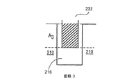
図2〜図4を参照すると、一実施形態に従って構築され、微細加工された移植可能な圧力センサーに用いられるように構成された可変コンデンサー200は、基板210、基板210に置かれた柔軟性のある部材220、および柔軟性のある部材220から間接的に延びた複数のコンデンサー要素232を含むコンデンサー部品230を含む。コンデンサー要素232は、基板230にわたって規定される溝、筋またはチャネル(一般的にチャネル216)内で、例えば、図2〜図4に示されるように、部分的に基板230にわたって可動である。例示された実施形態において、コンデンサー要素232のすべては同じ長さであるが、他のコンデンサー要素232の構成を用いてもよい。
2-4, a
コンデンサー要素232のチャネル216内での種々の深さへの動作により、コンデンサー要素232および基板220の重なり合う面積が変化する。重なり合う面積が変化すると、可変コンデンサー200を含むセンサー回路の静電容量および共鳴周波数応答が変化する。例えば、図3は、重なり合う面積がA1となる第一の深さに位置する複数のコンデンサー要素またはコンデンサー極板232を例示する一方、コンデンサー要素232がチャネル216内により深く動かされた場合、重なり合う面積はΔAだけ増加しA2となる。
Operation of the
基板210はシリコンから構成されていてよく、約500ミクロンの厚さを有しているウェハーの形状をしていてよい。この仕様はシリコンに関するが、基板210は導電性ポリマーまたは十分に高い導電率を有した他の適した微細加工可能な基板を含む他の材料から構成されていてよい。基板210は上面212および底面214を有している。1つ以上のチャネル216は基板の上面212にわたって形成されており、これにより対応する突起、壁またはフィンガー218が形成される。例示された実施形態において、チャネル216および突起218は櫛形構造を形成する。
The
例示された実施形態において、基板210は、複数のチャネル216を、例えば、5つのチャネル216、および4つの対応する突起物218を規定する。しかし、基板210は、他の数のチャネル216を、例えば、3〜10のチャネル216を規定してもよいことは理解されるべきである。チャネルの数は、コンデンサー200の構成、例えば、基板210の幅および/またはコンデンサー要素232の数に依存してもよい。更に、例示された実施形態には同じ幅のチャネル216および突起物218が示されているが、チャネル216および突起物218が異なる幅を有し、これにより異なる静電容量が提供されてもよく、異なる数のチャネル216および異なるコンデンサー要素232構成が収容されていてもよい。
In the illustrated embodiment, the
例えば、500ミクロンの基板210を含む実施形態においては、チャネル216のそれぞれが、約200ミクロンの深さ、約20ミクロンの幅、約20ミクロンの空間(突起部218の幅)を有していてよい。コンデンサー要素232はチャネル216内で約50ミクロン可動であり、その結果、約106〜約107平方ミクロンの範囲であってよい、コンデンサー要素232および基板210の重なり合う面積が得られる。必要に応じて他の寸法および構成を用いることができることは理解されるべきである。
For example, in an embodiment including a 500
柔軟性のある部材220には、外面すなわち上面221、および内面222が含まれる。第一および第二の縁すなわち底面223、224は、基盤210の上面212に、置かれ、接続され、形成され、またはシールされる。可変コンデンサー200の加工中、別の材料またはコーティング、例えば、二酸化ケイ素の層(図2〜図4に示されていない)は、基板210の上面212に取り付けられてもよい。従って、上面212よりもむしろ柔軟性のある部材220の縁223、224が、二酸化ケイ素層と直接接触していてよい。説明および例示を簡単にするため、図2〜図4では、その接触が中間二酸化ケイ素層の結果として、直接的であっても間接的であっても、縁223、224は、基板210の上面212に置かれ、接続され、または形成されているように示されている。
柔軟性のある部材220には、第一の縁および第二の縁223、224の間に延びる中央部分225も含まれる。中央部分225は基板210の上面212の上に持ち上がっており、これにより、柔軟性のある部材の上面212および内面222の間の内部空間すなわちチャンバー226が規定される。コンデンサー200は最終的にはシールされ、その結果内部空間またはチャンバー226もシールされ、固定された内圧またはチャンバー圧(Pc)を有している。
The
例示された実施形態において、中央部分225には、第一のおよび第二の弓形すなわち「肩」部分227、228が含まれる。例示される実施形態において、それぞれの肩部分227、228は、それぞれ第一および第二の縁223、224から内側上向きに、肩部分227、228の間に延びる中央部分229へと延びる。例示された実施形態において、中央部分229は平坦で、基板210の上面212と平行である一方、肩部分227、228は、中央部分229が基板210上に持ち上げられるように、なんらかの様式で(例えば、弓形形状を有していることによる結果として)上向きに延びる。中央部分225は他の形状を有していてもよく、基板210の上に中央部分229を持ち上げるために、必要に応じて肩部分227、228は弓形形状すなわち肩形状または他の形状であってよいことは理解されるべきである。
In the illustrated embodiment, the
柔軟性のある部材220は、中央部分225、例えば、コンデンサー200の構成および流圧の適用に依存して中央部分229および/または一つ以上の肩部分227、228を許容する材料からなり、その結果、流圧が内部チャンバー圧力(Pc)より大きい場合、この流圧(Pf)の下、中央部分225は変形し、たわみ、または曲がる(図4に示される)。柔軟性のある部材220は弾性的であり、外部流圧が内部チャンバー圧力より小さい場合、変形した形状(図4に示される)から初期状態または弛緩した状態(図3に示される)に戻る。
The
この目的のために、柔軟性のある部材220は、約1GPa〜約10GPa、例えば、約4GPaの適切なヤング率を有した材料より構成されていてよい。柔軟性のある部材120に適した材料の1つの例は、パリレン、例えば、パリレンC、D、N、F、HT、AおよびAMである。説明を簡単にするため、ポリマーまたはパリレンからなる柔軟性のある部材220を参照するが、柔軟性のある部材120は、望ましい柔軟性および/または弾性特性を提供する他の適した材料から構成されていてよい。柔軟性のある部材120の材料の選択もまた、例えば、微細加工の容易性、CMOS/MEMSプロセス適合性および生体適合性(例えば、米国薬局方ClassVIの移植可能なグレード)に依存していてもよい。
For this purpose, the
一実施形態において、柔軟性のある部材220はパリレンからなってよく、約500ミクロンの幅を有してもよく、肩部分227、228は、中央部分229が基板210の上面212の上に約10ミクロン持ち上がっているように構成されていてよい。中央部分225は、基板210に向かって約10ミクロン動くか、またはたわんでよい。これらの寸法は、持ち上げられた柔軟性のある部材220を有した可変コンデンサー200がどのように実装され得るかの一例として提供されるものであり、他の構成を異なる用途に用いることが可能であることは理解されるべきである。
In one embodiment, the
図2〜図4を参照し、更に図5を参照すると、コンデンサー要素232は、柔軟性のある部材220から間接的に延び、櫛形構造に配置されるフィンガーまたは平板の形態であってよい。例示された実施形態において、コンデンサー要素232は、1つ以上のクロスバー若しくは部材234から間接的に延びるか、または1つ以上のクロスバー若しくは部材234に備えられている。中間部材236は、柔軟性のある部材220およびクロスバーまたはクロス部材234の間に延びる。図2〜図4は、柔軟性のある部材220の中間セクション229とクロスバー部材234とを接続する単一の中間部材236を含む実施形態を例示する。チャンバー226の構成部分は、中間セクション229の内面222、クロスバー部材234、柔軟性のある部材とクロスバー部材234の間に延びる中間部材236により規定される。
With reference to FIGS. 2-4, and with further reference to FIG. 5, the
ある実施形態によると、中間部材236の数はコンデンサー要素232の数より少ない。例示された実施形態において、単一の中間部材236は、中間セクション229および複数のコンデンサー要素232を備えるクロスバー234を接合する。この構成により、十分な柔軟性を有した柔軟性のある部材220が有利に提供され、柔軟性のある部材220が変形した場合でも、コンデンサー要素232のチャネル216内での線形若しくは垂直な動作または実質的に線形若しくは垂直な動作が有利に提供される。
According to an embodiment, the number of
より具体的には、流圧による柔軟性のある部材220の変形により、柔軟性のある部材の下方向の動作、および柔軟性のある部材から延びる中間部材236の下方向の動作が得られる。これにより、中間部材236から延びるクロスバー234により備えられたコンデンサー要素232の下方向への動作が得られる。実施形態の構造構成により、コンデンサー要素232が柔軟性のある部材220から直接延びる場合(すなわち、公知の櫛形構造装置にあるように、いずれの中間部材236も存在しない)に起こり得るコンデンサー要素232の外側への反りが有利に防止され、これにより、コンデンサー要素232が、チャネル216の内面を擦るように、またはコンデンサー要素232がコンデンサーの構成によってはチャネル216内に位置しないようになる。従って、実施形態では、コンデンサー要素232が柔軟性のある部材間接的に延び、これによりコンデンサー要素232が、柔軟性のある部材220が流圧により、例えば、ボウル様形状に変形した場合、ある角度をなして押されることを防ぐように、中間部材236/クロスバー234構成が有利に利用される。
More specifically, deformation of
これらの利点を達成しつつ、他の構造構成を用いることができることは理解されるべきである。例えば、中間部材236の数量が十分な柔軟性を提供し、かつ、柔軟性のある部材220が変形した場合にコンデンサー要素232の垂直方向が保たれる限りにおいて、単一の中間部材236を有している代わりに、他の数量の中間部材236を用いることができる。
It should be understood that other structural configurations can be used while achieving these advantages. For example, having a single
例示された実施形態において、少なくとも一つのコンデンサー要素232は、中間部材236と一列に並び、または中間部材236により規定される同一の垂直平面内にあり、そして、少なくとも一つの他のコンデンサー要素232は、中間部材236により規定される垂直平面から離れた垂直平面内にある。例示された例において、中間のコンデンサー要素232は、中間部材236により規定される同一の平面内にあり、他のコンデンサー要素は、異なる垂直平面内にあり、中間部材236および中央のコンデンサー要素232により規定される平面と平行である。別の実施形態において、コンデンサー要素232は、いかなるコンデンサー要素232も中間部材236により規定される同一の垂直平面と一列に並ぶかまたはその平面内に存在することがないように配置されてよいが、すべてのコンデンサー要素232は中間部材236により規定される平面と平行である。用いられる特定の構成は、例えば、中間部材236の数、コンデンサー要素232の数、およびこれらの部品の配置に依存してよい。
In the illustrated embodiment, at least one
図5を参照すると、コンデンサー要素232は、柔軟性のある部材220と共にチャネル216内、例えば、対応する基板120の櫛形構造のチャネル内で動くことが可能なように構成され、かつ適した形状および大きさを有している。一実施形態によれば、コンデンサー要素232は、導電性材料510、例えば、金属であり、絶縁材料512によりコーティングされていてよい。別の実施形態において、コンデンサー要素232には、導電性の非金属材料上に塗布される金属コーティングが含まれていてよい。また、チャネル216は、絶縁コーティング520、および金属被覆法を用いてチャネル216内に塗布された導電性コーティングまたは金属コーティング522を含んでいてもよい。
Referring to FIG. 5, the
使用中、そこから延びているコンデンサー要素232を有している柔軟性のある部材220は、可変コンデンサー電極として用いられ、基板110は接地電極として用いられる。内部チャンバー226の圧力が外部流圧より大きい場合、柔軟性のある部材220は、変形したり、または曲がったりせず、その元の、または初期の形状を保持するだろう。流圧がチャンバー226の圧力を超える場合、中央部分229、例えば、柔軟性のある部材220の中間セクション225は、流圧により変形されまたはたわむ。柔軟性のある部材220は、中央部分229のたわみの量が外部流圧および内部チャンバー圧力の差((δ)(α)ΔP))に比例するように十分薄い(例えば、約10ミクロン)。同時に、柔軟性のある部材220から延びるコンデンサー要素232の位置は変化し、すなわち、コンデンサー要素232は、動いている柔軟性のある部材220と共に動く。
In use, the
結果として、互いにかみ合う電極間の有効な重なり合う面積が変化し、その結果として電極間の静電容量が変化する。より具体的には、コンデンサー要素232がそれぞれのチャネル216内でより深く動き、基板220およびコンデンサー要素232の重なり合う面積が増加するにつれて静電容量が増加し、コンデンサー要素232がチャネル216内でより浅い深さまで動き、基板220およびコンデンサー要素232の重なり合う面積が減少するにつれて静電容量が減少する。
As a result, the effective overlapping area between the interdigitated electrodes changes, and as a result, the capacitance between the electrodes changes. More specifically, the
例えば、図6を参照して、コンデンサー要素232は、一般に(0,0)と例示される、初期の、弛緩した位置にあってよい。初期の位置は、コンデンサー要素232がそれぞれのチャネル216内に部分的に位置するものであってよい。これに代わり、コンデンサー要素232は、チャネル216の上、例えば、例示された例において上面112の上の外側に位置してよい。初期の弛緩した位置は、可変コンデンサー200の構成、例えば、柔軟性のある部材220がどの程度変形しているかまたはたわんでいるか、およびコンデンサー要素232の長さに依存してよい。
For example, referring to FIG. 6, the
図7は、初期の弛緩した位置が、コンデンサー要素232の末端の構成部分が部分的にそれぞれのチャネル216の内側に位置している位置にある一実施例を例示している。チャンバー226の圧力が外部流圧よりも大きい場合、柔軟性のある部材220は初期の弛緩した状態であり、コンデンサー要素232はチャネル216内の第一の深さに位置する。この配置により、コンデンサー要素232および基板210の末端の構成部分の初期の重なり合う面積(A1)、対応する静電容量C1となる。
FIG. 7 illustrates one embodiment where the initial relaxed position is at a position where the terminal component of the
図6および図8を参照し、柔軟性のある部材220の外表面221上の流圧が増加すると、流圧は内部チャンバー226の圧力を超え、柔軟性のある部材220が基板210に向かって曲がり、または、たわむ。これによりコンデンサー要素232は、チャネル216内の初期の深さから第二のより深い深さへと動く。柔軟性のある部材220のこの動作により、コンデンサー要素232および基板210の重なり合う面積がA1からA2へと増加し、静電容量がC1からC2へと、対応して増加する。
With reference to FIGS. 6 and 8, as the fluid pressure on the
同様に、図6および図9に示されるように、更に流圧が増加すると、柔軟性のある部材220は、より大きく基板210に向かって曲がるか、またはたわみ、これにより、コンデンサー要素232をチャネル216内の第三の深さへと動かす。この動作により、コンデンサー要素232および基板210の重なり合う面積がA2からA3へと増加し、静電容量がC2からC3へと対応して増加する。
Similarly, as shown in FIGS. 6 and 9, as the fluid pressure further increases, the
この構造の静電容量挙動は、ΔC=(εA/d)(α)(β)(α)(ΔP)で表わすことができ、ここで、ΔC=(柔軟性のある部材220のたわみおよびチャネル216内の容量要素232の対応する動作に対する静電容量の変化);ε=(チャネル216の空間の誘電率);A=(コンデンサー要素232および基板210の重なり合う面積);d=(コンデンサー要素232の導電性構成部分510および基板210のチャネル216の導電性層520間の距離);αは比例係数であり、ΔP=(柔軟性のある部材220上の流圧の変化)である。
The capacitance behavior of this structure can be expressed as ΔC = (εA / d) (α) (β) (α) (ΔP), where ΔC = (flexure and channel of flexible member 220) Change in capacitance for corresponding operation of
図10は、静電容量の変化が柔軟性のある部材220上の流圧とどのように相関し得るかを例示したものである。例示された実施例において、0.4pFの静電容量の変化は、1mmHgの圧力変化に相当する。従って、実施形態により、感度1mmHgでの圧力測定が可能である。
FIG. 10 illustrates how the change in capacitance can correlate with the fluid pressure on the
全静電容量はC(全体)=C0+ΔC(ΔP)で表わすことができ、ここで、C(全体)=(全静電容量);C0=固定静電容量(ΔP=0の場合);ΔC=(柔軟性のある部材220上の圧力変化ΔPの関数としての静電容量の変化)、そしてΔP=(柔軟性のある部材220上の圧力変化)である。全静電容量は、可変コンデンサー200がテレメトリシステム(例えば、図1に一般的に例示されたシステム)に用いられることが可能なように十分高くあるべきである。全静電容量は、コンデンサー要素232の面積を増加させること(より大きな、電極の重なり合う面積)により、より多数のコンデンサー要素232を提供し、柔軟性のある部材220がチャネル216内でより深くたわみ重なり合う面積が増えるように柔軟性のある部材220を構築し、互いにかみ合う電極間の距離を減少させることにより、増加し得る。
The total capacitance can be expressed as C (overall) = C0 + ΔC (ΔP), where C (overall) = (total capacitance); C0 = fixed capacitance (when ΔP = 0); ΔC = (Capacitance change as a function of pressure change ΔP on flexible member 220) and ΔP = (Pressure change on flexible member 220). The total capacitance should be high enough so that the
効果的なテレメトリについての更なる検討には、結果として得られるセンサー回路の共鳴周波数が適切な検出範囲内に存在するように、十分に高いインダクタンスおよび十分に高い結合静電容量を備えた圧力センサーを有しているようにすることが含まれる。例えば、移植可能なセンサー回路の共鳴周波数は、生物医学的応用を含むテレメトリについては10〜500MHzの間にあるべきである。この目的のために、図1〜図10を参照して上で記載されるように可変コンデンサー200および十分な静電容量を有していることに加え、微細加工された移植可能な圧力センサーは、センサーを移植可能とし、生物医学的応用およびテレメトリで用いるのに適した電気的特性を提供することを可能とするインダクター要素も有するべきである。図11〜図15はランプインダクターまたは固定インダクタンスを有したインダクターを有した圧力センサーの異なる実施形態を例示したものである。
For further consideration of effective telemetry, a pressure sensor with sufficiently high inductance and sufficiently high coupling capacitance so that the resulting sensor circuit's resonant frequency is in the proper detection range. It is included to make it have. For example, the resonant frequency of an implantable sensor circuit should be between 10 and 500 MHz for telemetry including biomedical applications. For this purpose, in addition to having a
図11は、可変コンデンサー200を含む(明確さのために図11に例示されていない)微細加工された移植可能な圧力センサー1100に用いられる一実施形態に従って構築されたランプインダクター1110を例示する。更に、図12は、可変コンデンサー200およびインダクター1210がセンサー1200内にどのように統合され得るかを例示するために可変コンデンサー200の2つの面に沿う金属層1211を例示する透視断面図であるが、積み重なった金属層1211は、可変コンデンサー200の周りに配置されることは理解されるべきである。
FIG. 11 illustrates a
インダクター1110は、基板210の上面212内で統合され、可変コンデンサー200を取り囲む金属線1112により形成されている。例示された実施形態において、単一のワイヤー1112が可変コンデンサー200の周りに渦巻きパターンで巻かれている。図11に示されるインダクター1110の実装の一実施例には、約2ミクロンの厚さ、約20ミクロンの幅を有し、約5つの重なり合う部分を形成するように巻かれている金属線または金属要素1112が含まれてよい。重なり合う金属線1112は約10ミクロン離れた間隔がおかれていてよい。
The
図12を参照すると、別の実施形態において、微細加工された圧力センサー1200には、表面微細加工方法を用いて加工された金属層1211を重ね合わせたものとして形成されたインダクター1210が含まれる。この実施形態において、インダクター1210は、絶縁層1212および金属層1211が交互に積み重なりあうように配置される。このインダクター構成は、ランプインダクタンスおよびランプ静電容量が増加していることが必要とされる構成に特に適していてよい。絶縁層1212は、パリレンのようなポリマーまたは柔軟性のある部材220を形成するために用いられる同様の材料であってよい。金属層1211のすべては、絶縁材料1212内に埋め込まれていてよく、または金属層1211の最上層は露出(図12に示されるように)していてもよい。一実施形態において、インダクター1210には2〜4の金属層1211が含まれてよい。金属層1211の厚さは、約2ミクロンであってよく、金属層1211の幅は約20ミクロンであってよく、金属層1211の間の絶縁層1212の厚さは約2ミクロンであってよい。
Referring to FIG. 12, in another embodiment, a
図13を参照すると、感度および感知距離の双方の観点でのより高い感知能力についての品質(Q)因子を増加させるために、抵抗を減らしながらインダクタンスを増加させることが望ましい場合がある。この目的のために、微細加工された圧力センサー1300には、可変コンデンサー200(図1〜図10に示されるように)および高アスペクト比のインダクター1310が含まれていてよい。図13は、どのように可変コンデンサー200およびインダクター1310がセンサー1300内で統合されてよいかを例示するために、可変コンデンサー200の2つの側面に沿うインダクター1210要素を例示する透視断面図であるが、金属線1311は可変コンデンサー200の周りに配置されていることは理解されるべきである。
Referring to FIG. 13, it may be desirable to increase the inductance while reducing resistance to increase the quality (Q) factor for higher sensing capability in terms of both sensitivity and sensing distance. For this purpose, the
インダクターは、基板210の構成部分に完全にわたって形成されたチャネル216を充填する厚い金属線1311を含んでよい。別の実施形態において、金属線1311は、所望のインダクタンスおよび抵抗に依存して、基板210に部分的にわたって形成されたチャネル216を充填してよい。図13に示される高アスペクト比のインダクター1310の構成は、式、R=pL/A、ここで、p=(金属材料の抵抗率)、L=(金属線の長さ)、A=(金属線の面積)、に基づき、厚い金属線1311の寸法の結果として、抵抗を減少させつつ、センサー1300の静電容量およびインダクタンスを最大化させるのに、よく適合している。例えば、基板210の厚さは、約500ミクロンであってよく、金属線1311は基板210にわたって延び、これも約500ミクロンの深さを有してよく、金属線1311の幅は約20ミクロンであってよく、金属線1311は基板210の長さに沿って延び、例えば、約3ミリメートルであってよい。
The inductor may include a
図14および図15を参照すると、別の実施形態において、微細加工された圧力センサー1400には、可変コンデンサー200およびインダクターシートの形状のランプインダクター1410が含まれてよい。限定ではなく、例示の目的で、センサー1400は、図13に示される高アスペクト比のインダクター1310の金属線1311と結合したインダクターシート1410を有しているものとして示されている。他の実施形態において、インダクターシート1410は、唯一のインダクター要素として、または例えば、図11および図12に示されるように他のタイプのインダクターと組み合わせて用いることができる。従って、図14および図15は、どのように実施形態が実施され得るかの一例として提供される。
Referring to FIGS. 14 and 15, in another embodiment,
例示された実施形態において、インダクターシート1410は、円形状を有し(拡大した形状または弛緩した形状の場合)、金属層1411および絶縁層1412を交互に含む。金属層1411は、白金、チタン、金または他の適した生体適合性金属または導電性物質であってよい。絶縁層1412はパリレンのようなポリマーであってよい。
In the illustrated embodiment, the
インダクターシート1410は、好ましくは臨床用ゲージニードル(例えば、ゲージサイズが20〜25を有している)を介した移植のために構成されている。この目的のために、インダクターシート1410は、ニードルを介して送達される場合に圧力がかけられた形状または圧縮された形状をとり、センサー1400がニードルから展開され移植された後、拡大した形状または弛緩した形状をとるように構成されていてよい。例えば、インダクターシート1410は、ニードル内に位置する間は巻かれ折りたたまれていてよく、圧力センサー1400がニードルから展開された場合、拡大され、円形状(図14および図15に示されるように)をとってよい。
The
図16Aは、可変コンデンサー(例えば、図1〜図10に示される)およびランプインダクター(例えば、図13に示されるようなインダクター1310)を有した微細加工された圧力センサーの加工方法1600の実施形態を例示したものである。図16Aに示された方法のステップは、他の可変コンデンサーおよび他のランプインダクターを有している圧力センサー(例えば、図11、図12、図14および図15に示される)を加工するために用い、および/または適用することができることは理解されるべきである。説明を簡単にするために、図13に示される、可変コンデンサーおよびランプインダクターを有した圧力センサーの加工方法を参照する。
FIG. 16A illustrates an implementation of a
段階1605において、シリコンウェハーのような基板210が提供される。基板210は約500ミクロンの厚さを有していてよい。基板210は、例えば、DRIE(deep reactive-ion etching)でエッチングされる。例示された実施形態において、DRIEを用いて基板210の中央の構成部分を部分的にわたってエッチングし、(最終的な可変コンデンサー200のための)チャネルを形成し、基板210に完全にわたる他のチャネル216(最終的なインダクター1310)を形成することができる。基板210の中央の構成部分中のチャネル216の幅は約20ミクロンであってよく、基板210の中央の構成部分内のチャネル216の深さは約200ミクロンであってよい。また、基板210にわたって形成された他のチャネル216も、約20ミクロンでよい。組織アンカー(図16Aに示されていない)は、基板210の裏側214に作成されていてよい。適切な組織アンカーの一例が、「Micromachined Tissue Anchors for Securing Implants Without Sutures by E. Meng et al.,」と題する、米国特許公開第2006/0247664号に、記載されており、その内容が参照により本明細書に組みこまれている。
In
段階1610において、第一の絶縁層520(例えば、図5に示される)は、基板210の上面212上に蒸着される。絶縁層520はパリレンであってよく、約2ミクロンの厚さであってよい。図16Aに示されるように、第一のパリレン層520を適用しパターンを形成して、段階1605でのエッチングの結果として露出した表面を、すなわち、基板210に部分的におよび完全にわたり形成された開口チャネル216の内部表面をコーティングする。
In
段階1615において、基板210にわたって形成された開口チャネル216で金属電気めっきを行い、その結果、これらのチャネル216が金属1311で満たされる(図13で更に例示される)。これらの金属で満たされたチャネルまたはライン1311は、最終的に、基盤210内で統合される高アスペクト比のインダクター1310を形成する。
In
段階1620において、基板210に部分的にわたって形成されたチャネル216で表面金属被覆を行い、これにより第一のパリレン層520上に金属層522が形成される(図5に更に例示される)。
In
段階1625において、フォトレジスト1626の第一の犠牲コーティングを基板210の構成部分上に(例えば、スピンコーティングにより)適用する。第一のフォトレジストコーティング1626の厚さは約10ミクロンであってよい。実施形態に用いることができる一つの適切なフォトレジスト1626は、AZ4620タイプフォトレジスト(Clariant社、ノースカロライナ州シャーロットから供給される)の層である。フォトレジスト1626は、縁を滑らかにし脱気する目的で、約120℃でハードベイクしてよい。例示された実施形態において、第一のフォトレジストコーティング1626は、基板210を部分的にわたって形成された他の開口チャネル216の間に位置する金属充填チャネル1311上に適用される。
In
段階1630において、パリレンが適用され2度目のパターンが形成され、前に金属でコーティングされた開口チャネル216をパリレンで満し、フォトレジスト1626をパリレンでコーティングする。第二のパリレン層は約2ミクロンの厚さを有していてよく、最終的にコンデンサー要素232およびクロスバー234を形成するであろう(図2および図13に更に例示される)。
In
段階1635において、第二の犠牲フォトレジストコーティング1636が、コンデンサー要素232およびクロスバー234要素上、基板210の構成部分上、および金属1311で満たされたチャネル216上に適用され、パターンが形成される。第二のフォトレジストコーティング1636の厚さは、約15ミクロンであってよい。
In
段階1640において、金属充填チャネル216(インダクターワイヤー1311)およびコンデンサー要素または互いにかみ合う電極を接続するために、電極(明確にするために示されていない)上に金属接続が形成される。
In
段階1645において、パリレンが適用され3度目のパターンが形成される。第3のパリレンコーティングは約5ミクロンの厚さを有してよく、柔軟性のある部材220および柔軟性のある部材220と段階1635で形成されたクロスバー234要素との間に延びる中間部材236を形成する。例示された実施形態において、第3のパリレン層は、第2のフォトレジストコーティング1636、基板210および金属充填チャネル216の一部を覆う。第3のパリレンコーティングは、最終的に可変コンデンサー220を形成するであろうセクションおよび最終的にランプインダクター1310を形成するであろう他のセクション上に適用される。
In
段階1650において、基板210の裏側212が、例えば、DRIEを用いてエッチングされ、そして、段階1655において、段階1625および段階1630において適用された第1および第2のフォトレジスト層1626、1636が剥離され、これにより装置部品がリリースされる。
In
より具体的には、基板210の全体にわたって形成されたチャネル216を充填する金属1311は、高アスペクト比の固定インダクター1310(図13に更に例示される)を形成し、最上部の電極板またはコンデンサー要素232はクロスバー要素234により接合され、そして、クロスバー要素234および柔軟性のある部材220(図2〜図4および図13で更に例示される)の間に延びる中間部材236と接続され、底の電極板は、突起またはフィンガー218および対応するチャネル216を形成し、ここで、コンデンサー要素232が動き静電容量が変化する。
More specifically, the
加工方法ステップは一部を変更したり、または実施形態の他の構造の加工に適合することができることが理解されるべきである。インダクターは固定インダクター(例えば、図13に示される)であってよく、または、実施形態の方法を適用し、例えば、図16Bに示されるような、可変コンデンサー(上記されている)および可変インダクターを有している構造を加工することができる。図16Bに示されている可変インダクターは、シリコン基板210の更なるエッチング1660を行い、金属1311部品をリリースし可変インダクターを形成する、段階1660により形成することができる。従って、実施形態は、種々の可変コンデンサー/ランプインダクターおよび可変コンデンサー/可変インダクター構成の加工に適合させることができ、そして、図16A−Bは、どのように実施形態が実施され得るかの例を示すために提供されていることは理解されるべきである。
It should be understood that the processing method steps can be modified in part or adapted to the processing of other structures of the embodiments. The inductor may be a fixed inductor (eg, shown in FIG. 13) or by applying the method of the embodiment, for example, a variable capacitor (described above) and a variable inductor, as shown in FIG. 16B. The structure it has can be processed. The variable inductor shown in FIG. 16B can be formed by
図17は、図1〜図10に示される可変コンデンサーと図12〜図15に示される固定インダクタンスを有している異なるランプインダクターとを有する微細加工された圧力センサーの、期待される物理的、電気的および微小電気機械的な属性を要約した表である。図17内のデータは、有限要素法および一般的に認められた電気モデル計算を用いて導き出された。 FIG. 17 shows the expected physical properties of a micromachined pressure sensor having a variable capacitor shown in FIGS. 1-10 and a different lamp inductor having a fixed inductance shown in FIGS. Table summarizing electrical and microelectromechanical attributes. The data in FIG. 17 was derived using the finite element method and generally accepted electrical model calculations.
実施形態により、高い静電容量、インダクタンス、共鳴周波数(fr)、frシフト(Δf)および感度(Δf/fr)、並びに十分に低い抵抗を有している微細加工された圧力センサーが有利に提供される。例えば、図17は、図12に示される圧力センサー1200が高インダクタンス(約40nh)を有し、図13に示される圧力センサー1300が低い抵抗(約0.03ohm)および高いQファクター(〜600)を有し、そして図14に示される圧力センサー1400は高いインダクタンス(約145nh)および高い静電容量(約127pF)を有していることを示す。高アスペクト比のインダクター1310を含む圧力センサー1300は最も低い抵抗(〜0.03ohm)を有している。3つの圧力センサー1200、1300、1400すべての(ΔF/fr)の比は、10−3を超えると判定され、センサーの実施形態がテレメトリシステムの外部測定装置により検出するのに適しているであろうことを示した。
Embodiments advantageously provide a micromachined pressure sensor having high capacitance, inductance, resonant frequency (fr), fr shift (Δf) and sensitivity (Δf / fr), and sufficiently low resistance Is done. For example, FIG. 17 shows that the
また、図17は、実施形態に従って構築された微細加工された圧力センサーが、約1‐50mmHgの検出範囲を提供しつつ、約0.4pFの静電容量変化に対応する1mmHgの圧力変化を計測することができるように十分な感度を有しているはずであることを示している。また、図17は、実施形態に記載の可変コンデンサーおよびインダクターのサイズが有利に十分小さく、臨床用のゲージニードルを介して移植することが可能で、眼の種々の部位に移植することが可能である。例えば、可変コンデンサー200(図2〜図4)およびインダクター1210(図12)またはインダクター1310(図13)を有している圧力センサー1200は、約0.5mm x 0.5mm 3.0mmの寸法を有し、可変コンデンサー200(図2〜図4)および巻くことが可能なシートを含むインダクター1410を有している圧力センサー1400は、約0.5mm x 0.5mm x 4.0mmの寸法を有している(圧力がかけられた場合、または圧縮された構成にある場合)。また、所望により他の侵襲が最小限な切開、例えば、角膜を自己治癒させるように約3mm未満の角膜切開、を用いることができる。更に、例えば、上記で参照によりその内容が本明細書に組み入れられている米国特許出願公開第2006/0247664号に記載のように、組織アンカーを用い、縫合の必要なしに実施形態のセンサーを移植することができる。
FIG. 17 also shows that a micromachined pressure sensor constructed according to the embodiment measures a pressure change of 1 mm Hg corresponding to a capacitance change of about 0.4 pF while providing a detection range of about 1-50 mm Hg. It should have enough sensitivity to be able to. FIG. 17 also shows that the size of the variable capacitor and inductor described in the embodiment is advantageously sufficiently small, can be implanted through a clinical gauge needle, and can be implanted in various parts of the eye. is there. For example, a
図18は、可変コンデンサーおよびランプインダクター、例えば、図12に示されるインダクター1210を含む移植可能な微細加工された圧力センサーの別の実施形態を例示している。例示された実施形態において、基板210は固体基板(チャネル216を含まない)である。上記のように、基板210は、例えば、シリコン、導電性ポリマー、または十分に高い導電率を有した別の適した微細加工可能な基板材料から成ってよく、約500ミクロンの厚さを有していてよい。
FIG. 18 illustrates another embodiment of an implantable microfabricated pressure sensor that includes a variable capacitor and a lamp inductor, such as the
可変コンデンサー1810は、基板210の上面212に置かれた1つまたは2つ以上のコンデンサー要素1810により形成されている。コンデンサー要素1811は固定され動かない。また、可変コンデンサー1810は、柔軟性のある部材220によって備えられた、例えば、埋め込まれたコンデンサー要素1812を1つ以上含む。これらのコンデンサー要素1812は柔軟性のある部材220と共に可動である。
図18は、単一のコンデンサー要素1811またはコンデンサー極板が基板210の上面に位置しかつ基板210の長さ方向に沿って延び、単一のコンデンサー要素またはコンデンサー極板1812が柔軟性のある部材220に埋め込まれかつその長さ方向に沿って延びている実施形態を例示している。他の実施形態において、コンデンサー要素1811、1812は、多数の要素から成る。加えて、コンデンサー要素1812は柔軟性のある部材220内に埋め込まれているものとして示されているが、コンデンサー要素1812は、柔軟性のある部材220、例えば、柔軟性のある部材220の中間セクション229の上面221上に備えられている。図18は、コンデンサー要素1811、1812を、それぞれ、説明および例示を容易にするため、単一の部品およびコンデンサー要素1812が柔軟性のある部材220内に埋め込まれたものとして例示している。
18 shows that a
更に、センサー1800の加工中、別の材料、例えば、二酸化ケイ素1820の層(図18に示される)が、金属要素と基板210との間の絶縁を提供する目的で基板210の上面212に適用されていてよいことは理解されるべきである。従って、コンデンサー要素1811は、二酸化ケイ素1820に配置されていてよいが、コンデンサー要素1811は上面212上に存在することが言及され、それには上面212および上面212上に適用された二酸化ケイ素層1820上に直接存在することが含まれる。コンデンサー1818は最終的に密封され、その結果内部空間、または、チャンバー226もまた密封され、固定された内部圧力またはチャンバー圧力(Pc)を有する。
Further, during processing of
ランプインダクター1210は、図12に示されるように、表面微細加工された大量の金属層1211として構成されていてよい。図18は、インダクター1210が、パリレンのような絶縁材料で分離された、第一のすなわち最下部の層1211aおよび第二のすなわち最上層1211bを含む一実施形態を例示している。最下部の金属層1211aは、二酸化ケイ素1820層に置かれ、絶縁材料1212で覆われている一方、最上部の金属層1211bは絶縁材料1212に埋め込まれている。図19を参照すると、圧力センサー1900は、インダクタンスを必要に応じて増加させるために、更なる金属元素の層、例えば、層1211a〜層1211eを含んでいてよい。
As shown in FIG. 12, the
一実施形態において、最下部および最上部の金属層1211a、1211bは同じ厚み、例えば、2ミクロン、同じ幅、例えば、約20ミクロン、および同じ長さ、例えば、3ミリメートルを有していてよい。別の実施形態において、最下部の金属層1211aは、最上部の金属層1211bが埋め込まれている柔軟性のある部材220の柔軟性を保ちつつインダクタンスを増加させるために、最上部の金属層1211bよりも厚くてよい。例えば、最下部の層1211aは厚さ約2ミクロンを有し、最上層1211bは約0.5ミクロンの厚さを有してよい。
In one embodiment, the bottom and
使用中、チャンバー226の内部圧力が外部流圧を超える場合、柔軟性のある部材220は、元のまたは初期の形状を保持するであろう。しかし、流圧が内部チャンバー226圧力よりも大きい場合、柔軟性のある部材220は流圧によりたわみ、または変形し、これにより、少なくとも中間セクション229およびそこに埋め込まれているコンデンサー要素1812を、基板210の上面212に置かれた固定されたコンデンサー要素1811のより近くまで動かすだろう。コンデンサー要素1811と1812の間の空間が減少することにより静電容量は増加し、コンデンサー要素1811と1812の間の空間が増加することにより静電容量は減少するため、柔軟性のある部材220の動作により、静電容量およびセンサー回路1800の共鳴周波数応答が変化する。
In use, the
図20は、図18に示されるように構成され、基板210にわたって形成されたポート2010を含む、微細加工された移植可能な圧力センサー2000の別の実施形態を例示している。コンデンサー要素188は、要素1811aおよび1811bを、チャンバー226内およびポート2010のそれぞれの面に含む。図21を参照して以下に論じるように、ポート2010は、センサー2010の加工中に用いられる物質を排出するために用いることができる。
FIG. 20 illustrates another embodiment of a micromachined
図21は、可変コンデンサー、例えば、図18〜図20に示される可変コンデンサー1810、並びにランプインダクター、例えば、図12および図18〜図20に示されるインダクター1210を有した、実施形態の微細加工された圧力センサー2000の加工方法2100の流れ図である。しかし、方法2100は、他の可変コンデンサーおよびランプインダクター構成を有した他のセンサーを加工するように用いられおよび/または適合され得る。説明を容易にするため、図18および図20に示される可変コンデンサーおよびランプインダクターを有した圧力センサー2000の加工方法2100が参照される。
FIG. 21 illustrates a microfabrication of an embodiment having a variable capacitor, such as the
段階2105において、基板210、例えば、シリコンウェハーが提供される。基板210は約500ミクロンの厚さを有していてよい。基板210の最上部および最底部の表面212および214は、公知の熱酸化および酸化物パターン形成法により加工することができる。例えば、約1〜2ミクロンの厚さを有したウェット(wet)酸化物(例えば、二酸化ケイ素層1820)は、基板210の最上部および最下部の表面上に成長させることができる。
In
段階2110において、第一の金属層1211a、1811a、1811bは、基板210上、基板210の上面212上の二酸化ケイ素層1820上に蒸着される。第一の金属層1211aは、約2ミクロンの厚さを有していてよい。第一の金属層1211aは、約2ミクロンの厚さを有してよい。第一の金属層の構成部分1211aは、インダクター1210の一部を形成し、金属層の構成部分1811a、1811bは、可変コンデンサー1810の最底部または固定された部品を形成するであろう。
In
段階2115において、フォトレジスト2102の犠牲コーティングが第一の金属層の構成部分1811a、1811b上、二酸化ケイ素1820の構成部分上および基板210の構成部分上に適用(例えば、スピンコーティングにより)される。実施形態で用いることができる一つの適切なフォトレジストは、AZ4620タイプフォトレジスト(Clariant社シャーロット、ノースカロライナ州により供給されている)の層である。縁を滑らかにし脱気する目的で、フォトレジスト2102は、適用可能であれば、約120℃でハードベイクしてもよい。
In
段階2120において、シリコン基板210の上面212は、パリレンのシリコン基板210への接着を促進するために例えば、XeF2気相エッチングを用いて粗面化してよい。段階2125において、第一の層またはパリレン1212aのコーティングが蒸着されパターンが形成される。図21に示されるように、第一のパリレンコーティング1212aは、フォトレジスト2102上、および最終的にはランプインダクター1210の一部となる金属構成部分1212a上に塗布され、シリコン基板210と接触して密封を形成する。第一のパリレン層1212aは約2ミクロンの厚さを有していてよい。
In
段階2130において、第二の金属層1211bが第一のパリレン層1212a上に蒸着される。段階2135において、第二のパリレン層1212bが蒸着されパターンが形成される。第二の金属層1211bの構成部分がインダクター1210の一部を形成し、第二の金属層の別の構成部分1812は、柔軟性のある部材220により備えられ、共に可動であるコンデンサー要素を形成する。
In
段階2140において、表面微細加工プロセスおよびコーティングまたは層の蒸着後、シリコン材料はウェハー210の裏側211からエッチングにより取り除かれ、1つ以上のスルーホール、または開口、またはポート2010を形成する。段階2145において、フォトレジスト2102は、ポート2010を介して、例えば、アセトンを用いて剥離される。裏側のエッチングは、例えば、深堀り反応性イオンエッチング(deep reactive-ion etching)(DRIE)を用いて行ってもよい。結果としてこれにより柔軟性のある部材220がリリースされる。
In
図22は、更なる裏側のエッチングを段階2205において行い凹んだ窪み2203を形成することを除いて、図21に示される方法2100と同様の方法2200を例示している。凹んだ窪み2203は、圧力センサーのパッケージ後に被包空気量を有利に増加させる。
FIG. 22 illustrates a method 2200 that is similar to the
図23は、可変コンデンサー2310および可変インダクター2320を含む圧力センサーの2300の別の実施形態を例示する。例示された実施形態において、基板210は固体基板(チャネル216を含まない)である。可変コンデンサー2310は、基板210の上面212上にある1つ以上のコンデンサー要素により形成される。例示される実施形態には、固定され可動でない1つのコンデンサー要素1811が含まれる。1つ以上のコンデンサー要素1812は、柔軟性のある部材220に、例えば、そこに埋め込まれることにより備えられ、かつ、柔軟性のある部材220と共に可動である。
FIG. 23 illustrates another embodiment of a
図23は、単一のコンデンサー要素1811またはコンデンサー極板が基板210の上面212上に位置し、基盤210の長さ方向に沿って延び、単一のコンデンサー要素またはコンデンサー極板1812が柔軟性のある部材220に埋め込まれ、かつその長さ方向に沿って延びている実施形態を例示している。別の実施形態において、コンデンサー要素1811、1812は、複数の要素から成っていてよい。更に、コンデンサー要素1812は柔軟性のある部材220内に埋め込まれているものとして示されているが、コンデンサー要素1812もまた、例えば、柔軟性のある部材220の中間セクション229の最上部、または、外表面221上で、柔軟性のある部材220により備えられていてよい。図18は、説明を簡単にするため、それぞれのコンデンサー要素1811、1812を単一の部品として例示し、コンデンサー要素1812が柔軟性のある部材220内に埋め込まれているとして例示している。更に、図18に関して上記されるように、コンデンサー要素1811は、実際は二酸化ケイ素層1820上にあってよいが、上面212上に存在するものとして記載されている。
FIG. 23 shows that a
可変インダクター2320には、第一のまたは最底部の層1211およびこれもまた柔軟性のある部材220内に埋めこまれた、第二のまたは最上部の層1211bが含まれる。例えば、第一のまたは最底部の層1211aは、約2ミクロンの厚さを有した金属材料であってよく、最上部の層1211bは、約0.5ミクロンの厚さを有した金属材料であってよい。柔軟性のある部材220は、約5ミクロンの厚さを有してよい。柔軟性のある部材220の変形またはたわみにより、可変コンデンサー2310の構成部分が動き、また、可変インダクター2320の構成部分も動く。
The
より具体的には、内部チャンバー226の圧力が、外部流圧を超える場合、柔軟性のある部材220はその元のまたは初期の形状を保持するだろう。しかし、流圧が内部チャンバー226よりも大きい場合、柔軟性のある部材220は流圧によりたわみまたは変形し、これにより、少なくとも中間セクション229を動かし、それと同時に、そこに埋め込まれているコンデンサー要素1812及びインダクター要素1211bを動かす。コンデンサー要素1812は、流圧の変化に応じて基板210の上面212上に置かれた固定されたコンデンサー要素1811に近づくように、及びそこから離れるように動き、そして、インダクター要素1211bもまた、固定されたインダクター要素1211aに近づくように、及びそこから離れるように動かされ、これにより、同時に、センサー2300の静電容量、インダクタンス及び共鳴周波数応答が変化する。
More specifically, if the pressure in the
図24は、図23に示されるように構成され、基板210にわたって形成されたポート2010、ならびに、チャンバー226内およびポート2010のそれぞれの側上のコンデンサー要素1811aおよび1811bを含む、微細加工された移植可能な圧力センサーの別の実施形態を示す。図20及び21を参照して上記されるように、ポート2010はセンサー2400の加工中に用いられるフォトレジスト材料を排出するために用いることができる。図20に示されるセンサー2400を加工することのできる一つの方法が図25に例示されている。
FIG. 24 is a micromachined implant configured as shown in FIG. 23 and including a
図25を参照し、可変コンデンサー2310及び可変インダクター2320を有した微細加工された圧力センサー2400の加工方法2500には、ウェハーまたは基板210、例えば、シリコン基板を、段階2505で提供することが含まれる。基板210の最上部及び最底部の表面は、公知の熱酸化及び酸化物パターン形成法により処理される。例えば、約1〜2ミクロンの厚さを有したウェット酸化物(例えば、二酸化ケイ素層1820)は、シリコン基板210の最上部及び最底部の表面で成長し、パターン形成されることができる。
Referring to FIG. 25, a
段階2510に於いて、第一の金属層1211a、1811a、1811bは、基板210の上面212上の二酸化ケイ素層1820上に蒸着される。第一の金属層は、約2ミクロンの厚さを有してよい。第一の金属層の構成部分1211aは、インダクター1210の最底部のまたは固定された部品を形成し、金属層の構成部分1811a、1811bは、可変コンデンサー1810の最底部または固定された部品を形成するであろう。
In
段階2515において、フォトレジスト2102の犠牲コーティングが、第一の金属層の構成部分1211a、1811a、1811b上、二酸化ケイ素1820の構成部分、及び基板210の構成部分上に(例えば、スピンコーティングにより)適用される。フォトレジスト2102は約6ミクロンの厚さを有してよい。従って、例示される実施形態において、フォトレジスト2012は、金属層全体にわたって適用されるが、その一方、例えば、図21および図22に示される実施形態において、フォトレジスト2102は、インダクター2110の一部を形成するだろう構成部分1211a上に適用されない。
In step 2515, a sacrificial coating of
段階2520に於いて、シリコン基板210の上面212は、例えば、XeF2気相エッチングを用いて粗面化してよく、段階2520において、第一の層またはパリレンのコーティング1212aが蒸着され、パターン形成される。図25に示されるように、第一のパリレンコーティング1212aはフォトレジスト2102の全体にわたって適用され、基板210に接触し、密封が形成される。第一のパリレン層1212aは約2ミクロンの厚さを有してよい。
In
段階2530において、第二の金属層1211b、1812が、第一のパリレン層1212a上に蒸着される。第二の金属層1211bは可変インダクター2320の一部を形成し、第二の金属層の別の構成部分1812は、可変コンデンサー2310の一部を形成し、その双方が柔軟性のある部材220により備えられ、これと共に可動である。
In
段階2535において、第二のパリレン層1212bは、第二の金属層1211b、1812上に蒸着され、パターン形成される。段階2540において、表面微細加工プロセスおよびコーティングまたは層の蒸着後、シリコン材料がウェハー210の裏側211からエッチングにより取り除かれ、1つ以上のスルーホール、または開口、またはポート2000が形成され、そして、段階2545において、フォトレジスト2102が、ポート2000を介して例えば、アセトンを用いて剥離される。裏側のエッチングは例えば、深堀り反応性イオンエッチング(deep reactive-ion etching)(DRIE)を用いて行うことができる。この結果、これにより、外部流圧に依存して動くことができる柔軟性のある部材220がリリースされる。また、図25は、更なる裏側のエッチングが段階2550において行われ、窪んだ凹み2203が形成され、これにより圧力センサーのパッケージ後、被包空気量が有用に増加し得る実施形態が例示する。方法2100工程を用いおよび/または適合することで、可変コンデンサー2310および可変インダクター2320の構成を加工することが可能であることは理解されるべきであり、説明を容易にするため、図23および図24に示されるように可変コンデンサー2310およびランプインダクター2320を有する圧力センサーの加工方法が参照される。
In
特定の実施形態が示され記載されているが、上で議論されたことはこれらの実施形態の範囲を限定することを意図するものではないことは理解されるべきである。実施形態の精神および範囲を逸脱せずに種々の変更及び改変が可能である。例えば、圧力センサーには、可変コンデンサー及びランプインダクター、または可変コンデンサー及び可変インダクターが含まれてよい。さらに、可変コンデンサー、ランプインダクター及び可変インダクター部品の寸法及び構成は、実施形態がどのように実施されるかの例として提供され、その他の寸法や構成を圧力検出の仕様や用途に適するように使用してよい。さらに、加工プロセスのパラメータ及び工程は、異なるコンデンサー及びインダクター構成を加工する場合変わり得る。実施形態は、ポリマー、例えば、パリレンを参照して記載されるが、柔軟性のある部材及びコンデンサー要素は、他の材料、例えば、生体適合性金属であってよく、同じ材料でも異なる材料でもよい。また、実施形態は、基板内に形成されたチャネル内で可動なコンデンサー要素を有した可変コンデンサーと共に、および、基板チャネルなしに実装される可変コンデンサーと共に用いることもできる。 Although specific embodiments have been shown and described, it should be understood that what has been discussed above is not intended to limit the scope of these embodiments. Various changes and modifications can be made without departing from the spirit and scope of the embodiments. For example, the pressure sensor may include a variable capacitor and a lamp inductor, or a variable capacitor and a variable inductor. In addition, the dimensions and configurations of variable capacitors, lamp inductors and variable inductor components are provided as examples of how the embodiments may be implemented, so that other dimensions and configurations are suitable for pressure sensing specifications and applications. May be used. Furthermore, the processing process parameters and steps may vary when processing different capacitor and inductor configurations. Embodiments are described with reference to a polymer, eg, parylene, but the flexible member and capacitor element may be other materials, eg, biocompatible metals, which may be the same or different materials. . Embodiments can also be used with variable capacitors having capacitor elements movable within channels formed in the substrate and with variable capacitors mounted without the substrate channel.
ニードルを介してセンサーを送達することによる縫合なしの眼へのセンサーの移植が参照されるが、他の侵襲が最小限の移植手順及び装置を、必要に応じて用いることができることは理解されるべきである。例えば、センサー装置は、角膜又は強膜を適切な大きさに切開することにより移植することができる。センサー装置は組織アンカーまたはフックを用いて移植することもできる。実施形態は種々の生物医学的応用に用いることができることも理解すべきである。テレメトリを用いた眼内圧を受動的にモニタリングするための微細加工された圧力センサーが参照されるが、実施形態は、他の体液の圧力および生理学的パラメータのモニタリング、例えば、動脈瘤内の血圧のモニタリング脳脊髄液圧のモニタリング、および他の生物医学的応用での圧力のモニタリングを含むがそれらに限定されない他の用途にも利用され、または適用されてよい。従って、実施形態には、代替物、改変物、及び特許請求の範囲内の均等物が含まれていることが意図されている。 Although reference is made to implanting a sensor into an eye without suture by delivering the sensor through a needle, it is understood that other minimally invasive implantation procedures and devices can be used as needed. Should. For example, the sensor device can be implanted by cutting the cornea or sclera to an appropriate size. The sensor device can also be implanted using tissue anchors or hooks. It should also be understood that the embodiments can be used in a variety of biomedical applications. While reference is made to microfabricated pressure sensors for passively monitoring intraocular pressure using telemetry, embodiments may be used to monitor the pressure of other body fluids and physiological parameters, such as the blood pressure in an aneurysm. Monitoring Cerebrospinal fluid pressure monitoring, and other uses, including but not limited to pressure monitoring in other biomedical applications, may be utilized or applied. Accordingly, the embodiments are intended to include alternatives, modifications and equivalents within the scope of the claims.
Claims (20)
複数のチャネルを規定する基板と;
基板上の平行な第1および第2の縁と、前記第1の縁および第2の縁の間に延び前記基板の上に持ち上げられた中央部分とを有し、前記基板と中央部分との間に密封されたチャンバーを部分的に規定する、柔軟性のある部材と;
少なくとも1の中間部材を介して前記柔軟性のある部材から間接的に延びる複数の平行なコンデンサー要素であって、それぞれのチャネル内で前記柔軟性のある部材の外表面上の流圧の変化に応じて可動であり、静電容量が複数のコンデンサー要素と前記基板との重なり合う面積の変化に応じて変化するコンデンサー要素とを含み、前記中央部分の変形によって、前記複数のコンデンサー要素がそれぞれのチャネル内で前記基板の上面により規定される平面に対して垂直な方向に動く、可変コンデンサー。 A micromachined implantable pressure sensor variable capacitor,
A substrate defining a plurality of channels;
A parallel first and second edge on the substrate and a central portion extending between the first and second edges and raised above the substrate, the substrate and the central portion A flexible member partially defining a chamber sealed between;
A plurality of parallel condenser elements extending indirectly from the flexible member via at least one intermediate member , wherein a change in fluid pressure on the outer surface of the flexible member is within each channel; depending is movable, viewed contains a capacitor element that changes according to the change of the area capacitance overlapping with a plurality of capacitor elements and the substrate, by deformation of said central portion, said plurality of capacitor elements each A variable capacitor that moves in a channel in a direction perpendicular to a plane defined by the top surface of the substrate .
複数のチャネルを規定する基板と、基板に設けられた平行な第1の縁および第2の縁並びに前記第1の縁および第2の縁の間に延びる中央部分を備えた柔軟性のある部材とを具え、前記中央部分は前記基板の上に持ち上がっており、密封されたチャンバーが前記基板および前記中央部分の間に規定されており、少なくとも1の中間部材を介して前記柔軟性のある部材から間接的に延びる複数のコンデンサー要素を含む可変コンデンサーを具え、前記複数のコンデンサー要素は前記柔軟性のある部材の外表面上の流圧の変化に応じてそれぞれのチャネル内で可動であり、静電容量は前記複数のコンデンサー要素および前記基板の重なりあう面積の変化に応じて変化し、前記中央部分の変形によって、前記複数のコンデンサー要素がそれぞれのチャネル内で前記基板の上面により規定される平面に対して垂直な方向に動き;さらに
前記可変コンデンサーと電気的に接続されたインダクターを含み、
前記可変コンデンサーおよび前記インダクターを含む電気回路が、前記柔軟性のある部材の外表面上の流圧の変化に応じて、検出可能な共振周波数シフトを生成するように構成されている、圧力センサー。 A micromachined implantable pressure sensor comprising:
A flexible member comprising a substrate defining a plurality of channels, and parallel first and second edges provided on the substrate and a central portion extending between the first and second edges The central portion is raised above the substrate, a sealed chamber is defined between the substrate and the central portion, and the flexible member via at least one intermediate member A variable capacitor including a plurality of capacitor elements indirectly extending from the plurality of capacitor elements, the plurality of capacitor elements being movable in respective channels in response to changes in fluid pressure on the outer surface of the flexible member. electrostatic capacitance changes according to the change in the area of overlapping of the plurality of capacitor elements and the substrate, by deformation of said central portion, said plurality of capacitor elements each Ji Further includes a said variable capacitor and electrically connected to the inductor; motion in a direction perpendicular to the plane defined by the upper surface of the substrate in the channel
A pressure sensor, wherein an electrical circuit including the variable capacitor and the inductor is configured to generate a detectable resonant frequency shift in response to changes in fluid pressure on the outer surface of the flexible member.
基板と;
前記基板の上に配置された柔軟性のある部材と、前記基板と前記柔軟性のある部材の間に規定されるチャンバーと;
可変コンデンサーと;
前記可変コンデンサーと電気的に接続された可変インダクターとを具え、
前記柔軟性のある部材が前記可変コンデンサーの第1要素および前記可変インダクターの第1要素を担持し、前記可変コンデンサーの第2要素および前記可変インダクターの第2要素が前記基板上に配置され、前記柔軟性のある部材が前記柔軟性のある部材の外表面上の流圧変化に応じて可動であり、その動きにより前記可変コンデンサーおよび前記可変インダクターの第1要素がそれぞれ前記可変コンデンサーおよび前記可変インダクターの第2要素に近づくようにまたは離れるように動くことで、静電容量およびインダクタンスを変化させる、圧力センサー。 A micromachined implantable pressure sensor comprising:
A substrate;
A flexible member disposed on the substrate; and a chamber defined between the substrate and the flexible member;
With variable capacitors;
A variable inductor electrically connected to the variable capacitor;
The flexible with some members said carries a first element of the first element and the variable inductor of the variable capacitor, the second element of the second element and the variable inductor of the variable capacitor is disposed on the substrate, wherein A flexible member is movable in response to a change in fluid pressure on the outer surface of the flexible member, and the first element of the variable capacitor and the variable inductor is moved by the movement to the variable capacitor and the variable inductor, respectively. A pressure sensor that changes capacitance and inductance by moving toward or away from the second element of the sensor.
外部機器を用いて信号を発生させるステップと;
前記発生させた信号により、眼内に移植された圧力センサーに通電するステップとを具え、前記圧力センサーは、(i)基板上の少なくとも1の縁と、前記少なくとも1の縁に隣接するとともに前記基板の上に持ち上げられた中央部分とを有し、前記基板と中央部分との間に密封されたチャンバーを少なくとも部分的に規定する、柔軟性のある部材と、(ii)可変インダクターおよび可変コンデンサーとを具え、前記柔軟性のある部材が前記可変コンデンサーの第1要素および前記可変インダクターの第1要素を担持し、前記可変コンデンサーの第2要素および前記可変インダクターの第2要素が前記基板上に配置され、前記柔軟性のある部材が当該柔軟性のある部材の外表面上の流圧変化に応じて可動であり、その動きにより前記可変コンデンサーおよび前記可変インダクターの第1要素がそれぞれ前記可変コンデンサーおよび前記可変インダクターの第2要素に近づくようにまたは離れるように動くことで、静電容量およびインダクタンスを変化させるものであり;さらに、
前記外部機器により発生させた信号と前記圧力センサーの間の相互作用を測定するステップと;
前記測定された相互作用に基づく眼内圧を決定するステップとを具える方法。 A method for measuring intraocular pressure,
Generating a signal using an external device;
Energizing a pressure sensor implanted in the eye with the generated signal, the pressure sensor comprising : (i) at least one edge on a substrate and adjacent to the at least one edge and the A flexible member having a central portion raised above the substrate and at least partially defining a sealed chamber between the substrate and the central portion; and (ii) a variable inductor and a variable capacitor The flexible member carries a first element of the variable capacitor and a first element of the variable inductor, and the second element of the variable capacitor and the second element of the variable inductor are on the substrate. And the flexible member is movable in response to a change in fluid pressure on the outer surface of the flexible member, and the variable Condensers and said variable first element of the inductor that move like or away so as to approach the second element of each of the variable capacitor and the variable inductor is intended to change the capacitance and inductance; Furthermore,
Measuring an interaction between a signal generated by the external device and the pressure sensor;
Determining an intraocular pressure based on the measured interaction.
Applications Claiming Priority (3)
| Application Number | Priority Date | Filing Date | Title |
|---|---|---|---|
| US84111306P | 2006-08-29 | 2006-08-29 | |
| US60/841,113 | 2006-08-29 | ||
| PCT/US2007/077156 WO2008027996A2 (en) | 2006-08-29 | 2007-08-29 | Microfabricated implantable wireless pressure sensor for use in biomedical applications and pressure measurement and sensor implantation methods |
Publications (2)
| Publication Number | Publication Date |
|---|---|
| JP2010503220A JP2010503220A (en) | 2010-01-28 |
| JP5307008B2 true JP5307008B2 (en) | 2013-10-02 |
Family
ID=39136850
Family Applications (1)
| Application Number | Title | Priority Date | Filing Date |
|---|---|---|---|
| JP2009526897A Expired - Fee Related JP5307008B2 (en) | 2006-08-29 | 2007-08-29 | Microfabricated implantable wireless pressure sensor and pressure measurement and sensor implantation method for biomedical applications |
Country Status (6)
| Country | Link |
|---|---|
| US (3) | US7900518B2 (en) |
| EP (2) | EP2786701B1 (en) |
| JP (1) | JP5307008B2 (en) |
| ES (1) | ES2565987T3 (en) |
| MX (1) | MX2009002193A (en) |
| WO (1) | WO2008027996A2 (en) |
Families Citing this family (97)
| Publication number | Priority date | Publication date | Assignee | Title |
|---|---|---|---|---|
| EP2786701B1 (en) | 2006-08-29 | 2015-12-23 | California Institute of Technology | Microfabricated implantable wireless pressure sensor for use in biomedical applications and pressure measurement and sensor implantation methods |
| US7677107B2 (en) * | 2007-07-03 | 2010-03-16 | Endotronix, Inc. | Wireless pressure sensor and method for fabricating wireless pressure sensor for integration with an implantable device |
| US7980145B2 (en) * | 2007-12-27 | 2011-07-19 | Y Point Capital, Inc | Microelectromechanical capacitive device |
| EP3108933B1 (en) | 2008-01-07 | 2019-09-18 | Salutaris Medical Devices, Inc. | Devices for minimally-invasive extraocular delivery of radiation to the posterior portion of the eye |
| US10022558B1 (en) | 2008-01-07 | 2018-07-17 | Salutaris Medical Devices, Inc. | Methods and devices for minimally-invasive delivery of radiation to the eye |
| US8602959B1 (en) | 2010-05-21 | 2013-12-10 | Robert Park | Methods and devices for delivery of radiation to the posterior portion of the eye |
| US8608632B1 (en) | 2009-07-03 | 2013-12-17 | Salutaris Medical Devices, Inc. | Methods and devices for minimally-invasive extraocular delivery of radiation and/or pharmaceutics to the posterior portion of the eye |
| US9873001B2 (en) | 2008-01-07 | 2018-01-23 | Salutaris Medical Devices, Inc. | Methods and devices for minimally-invasive delivery of radiation to the eye |
| US9056201B1 (en) | 2008-01-07 | 2015-06-16 | Salutaris Medical Devices, Inc. | Methods and devices for minimally-invasive delivery of radiation to the eye |
| EP2471572A3 (en) | 2008-04-17 | 2012-10-17 | Allergan, Inc. | Implantable access port device |
| US9023063B2 (en) | 2008-04-17 | 2015-05-05 | Apollo Endosurgery, Inc. | Implantable access port device having a safety cap |
| US8926524B2 (en) * | 2008-06-02 | 2015-01-06 | California Institute Of Technology | System, apparatus and method for biomedical wireless pressure sensing |
| DE102008033805A1 (en) * | 2008-07-18 | 2010-01-21 | Neue Magnetodyn Gmbh | A system for acquiring readings in or on an organism and method for making a component of that system |
| JP2010075325A (en) * | 2008-09-25 | 2010-04-08 | Fujifilm Corp | Endoscope soft part and endoscope |
| US8069730B2 (en) * | 2008-11-14 | 2011-12-06 | Kulite Semiconductor Products, Inc. | Pressure transducer structures suitable for curved surfaces |
| USD691269S1 (en) | 2009-01-07 | 2013-10-08 | Salutaris Medical Devices, Inc. | Fixed-shape cannula for posterior delivery of radiation to an eye |
| USD691268S1 (en) | 2009-01-07 | 2013-10-08 | Salutaris Medical Devices, Inc. | Fixed-shape cannula for posterior delivery of radiation to eye |
| USD691270S1 (en) | 2009-01-07 | 2013-10-08 | Salutaris Medical Devices, Inc. | Fixed-shape cannula for posterior delivery of radiation to an eye |
| USD691267S1 (en) | 2009-01-07 | 2013-10-08 | Salutaris Medical Devices, Inc. | Fixed-shape cannula for posterior delivery of radiation to eye |
| US9222819B2 (en) | 2009-02-20 | 2015-12-29 | University Of Southern California | Tracking and controlling fluid delivery from chamber |
| US20110303016A1 (en) * | 2009-02-24 | 2011-12-15 | University Of Southern California | Flexible polymer-based encapsulated-fluid devices |
| US8715158B2 (en) * | 2009-08-26 | 2014-05-06 | Apollo Endosurgery, Inc. | Implantable bottom exit port |
| US8708979B2 (en) | 2009-08-26 | 2014-04-29 | Apollo Endosurgery, Inc. | Implantable coupling device |
| US8506532B2 (en) * | 2009-08-26 | 2013-08-13 | Allergan, Inc. | System including access port and applicator tool |
| US8257295B2 (en) * | 2009-09-21 | 2012-09-04 | Alcon Research, Ltd. | Intraocular pressure sensor with external pressure compensation |
| US8212218B2 (en) * | 2009-11-30 | 2012-07-03 | International Business Machines Corporation | Dosimeter powered by passive RF absorption |
| WO2011082314A2 (en) | 2009-12-30 | 2011-07-07 | Brockman Holdings Llc | System, device, and method for determination of intraocular pressure |
| US20110196195A1 (en) * | 2010-02-05 | 2011-08-11 | Allergan, Inc. | Implantable subcutaneous access port |
| US8882728B2 (en) * | 2010-02-10 | 2014-11-11 | Apollo Endosurgery, Inc. | Implantable injection port |
| US8992415B2 (en) | 2010-04-30 | 2015-03-31 | Apollo Endosurgery, Inc. | Implantable device to protect tubing from puncture |
| US20110270025A1 (en) | 2010-04-30 | 2011-11-03 | Allergan, Inc. | Remotely powered remotely adjustable gastric band system |
| US20110270021A1 (en) | 2010-04-30 | 2011-11-03 | Allergan, Inc. | Electronically enhanced access port for a fluid filled implant |
| US8397578B2 (en) | 2010-06-03 | 2013-03-19 | Medtronic, Inc. | Capacitive pressure sensor assembly |
| US9737657B2 (en) | 2010-06-03 | 2017-08-22 | Medtronic, Inc. | Implantable medical pump with pressure sensor |
| US9408555B2 (en) | 2010-06-30 | 2016-08-09 | Indiana University Research And Technology Corporation | Supersensitive linear pressure transducer |
| EP3549617B1 (en) | 2010-07-12 | 2023-09-13 | University of Southern California | Biocompatible substrate for facilitating interconnections between stem cells and target tissues and methods for implanting same |
| EP2412305A1 (en) * | 2010-07-30 | 2012-02-01 | Ophtimalia | Integrated flexible passive sensor in a soft contact lens for IOP monitoring |
| US20120041258A1 (en) | 2010-08-16 | 2012-02-16 | Allergan, Inc. | Implantable access port system |
| US20120065460A1 (en) | 2010-09-14 | 2012-03-15 | Greg Nitka | Implantable access port system |
| US8966990B2 (en) * | 2011-02-11 | 2015-03-03 | Purdue Research Foundation | MEMS devices exhibiting linear characteristics |
| WO2012137067A2 (en) * | 2011-04-07 | 2012-10-11 | Oculox Technology | Intraocular pressure monitoring device and methods |
| US8877489B2 (en) | 2011-12-05 | 2014-11-04 | California Institute Of Technology | Ultrathin parylene-C semipermeable membranes for biomedical applications |
| WO2012149468A2 (en) | 2011-04-29 | 2012-11-01 | University Of Southern California | Instruments and methods for the implantation of cell-seeded substrates |
| US8821373B2 (en) | 2011-05-10 | 2014-09-02 | Apollo Endosurgery, Inc. | Directionless (orientation independent) needle injection port |
| US8801597B2 (en) | 2011-08-25 | 2014-08-12 | Apollo Endosurgery, Inc. | Implantable access port with mesh attachment rivets |
| WO2013059195A1 (en) * | 2011-10-17 | 2013-04-25 | Elenza, Inc. | Methods, apparatus, and system for triggering an accommodative implantable ophthalmic device based on changes in intraocular pressure |
| US9199069B2 (en) | 2011-10-20 | 2015-12-01 | Apollo Endosurgery, Inc. | Implantable injection port |
| US8858421B2 (en) | 2011-11-15 | 2014-10-14 | Apollo Endosurgery, Inc. | Interior needle stick guard stems for tubes |
| US9089395B2 (en) | 2011-11-16 | 2015-07-28 | Appolo Endosurgery, Inc. | Pre-loaded septum for use with an access port |
| US9248013B2 (en) | 2011-12-05 | 2016-02-02 | California Institute Of Technology | 3-Dimensional parylene scaffold cage |
| WO2013090231A1 (en) | 2011-12-13 | 2013-06-20 | Alcon Research, Ltd. | Active drainage systems with dual-input pressure-driven valves |
| US9339187B2 (en) | 2011-12-15 | 2016-05-17 | Alcon Research, Ltd. | External pressure measurement system and method for an intraocular implant |
| WO2014043418A1 (en) * | 2012-09-12 | 2014-03-20 | Innovative In Vivo Sensing, Llc | Strain sensor device with a biological substrate and method of manufacturing thereof |
| US9572712B2 (en) | 2012-12-17 | 2017-02-21 | Novartis Ag | Osmotically actuated fluidic valve |
| US9528633B2 (en) | 2012-12-17 | 2016-12-27 | Novartis Ag | MEMS check valve |
| US9295389B2 (en) | 2012-12-17 | 2016-03-29 | Novartis Ag | Systems and methods for priming an intraocular pressure sensor in an intraocular implant |
| US9487386B2 (en) * | 2013-01-16 | 2016-11-08 | Infineon Technologies Ag | Comb MEMS device and method of making a comb MEMS device |
| FR3001377B1 (en) * | 2013-01-25 | 2015-01-23 | Ophtimalia | INTEGRATED FLEXIBLE PASSIVE SENSOR CONTACT LENS |
| US10016132B2 (en) * | 2013-03-07 | 2018-07-10 | The Board Of Trustees Of The Leland Stanford Junior University | Implantable micro-fluidic device for monitoring of intra-ocular pressure |
| US10226552B2 (en) | 2013-04-04 | 2019-03-12 | Arizona Board Of Regents On Behalf Of The Unviersity Of Arizona | Materials, systems, devices, and methods for endoluminal electropolymeric paving and sealing |
| US9848775B2 (en) | 2013-05-22 | 2017-12-26 | The Board Of Trustees Of The Leland Stanford Junior University | Passive and wireless pressure sensor |
| US9962084B2 (en) * | 2013-06-15 | 2018-05-08 | Purdue Research Foundation | Wireless interstitial fluid pressure sensor |
| US9781842B2 (en) | 2013-08-05 | 2017-10-03 | California Institute Of Technology | Long-term packaging for the protection of implant electronics |
| US9226851B2 (en) | 2013-08-24 | 2016-01-05 | Novartis Ag | MEMS check valve chip and methods |
| CN104697702B (en) * | 2013-12-04 | 2017-06-13 | 中芯国际集成电路制造(上海)有限公司 | MEMS and forming method thereof |
| US20160302729A1 (en) | 2013-12-11 | 2016-10-20 | The Board Of Regents Of The University Of Texas System | Devices and methods for parameter measurement |
| US10499822B2 (en) * | 2014-05-09 | 2019-12-10 | The Royal Institution For The Advancement Of Learning / Mcgill University | Methods and systems relating to biological systems with embedded mems sensors |
| US9939331B2 (en) | 2014-05-21 | 2018-04-10 | Infineon Technologies Ag | System and method for a capacitive thermometer |
| US9322685B2 (en) * | 2014-06-30 | 2016-04-26 | The Boeing Company | MEMS-based conformal air speed sensor |
| CN106714664A (en) | 2014-07-01 | 2017-05-24 | 注射感知股份有限公司 | Hermetically sealed implant sensors with vertical stacking architecture |
| WO2016004223A1 (en) | 2014-07-01 | 2016-01-07 | Cao Ariel | Methods and devices for implantation of intraocular pressure sensors |
| EP4029425A1 (en) * | 2014-08-20 | 2022-07-20 | California Baptist University | Systems and methods for monitoring eye health |
| FR3025311B1 (en) | 2014-08-26 | 2016-12-30 | Commissariat Energie Atomique | PRESSURE SENSOR OF A FLUID |
| WO2016057796A1 (en) | 2014-10-08 | 2016-04-14 | The Arizona Board Of Regents On Behalf Of The University Of Arizona | Flowable electronics |
| EP3017749A1 (en) | 2014-11-06 | 2016-05-11 | Ophtimalia | Passive sensing means for a physiological parameter monitoring system |
| US10845620B2 (en) | 2014-12-08 | 2020-11-24 | Aleksandr Shtukater | Smart contact lens |
| CN107529985B (en) | 2015-03-31 | 2020-03-31 | 加州理工学院 | Biocompatible encapsulation for long-term implantable sensors and electronics |
| US10104478B2 (en) * | 2015-11-13 | 2018-10-16 | Infineon Technologies Ag | System and method for a perpendicular electrode transducer |
| ITUB20160704A1 (en) * | 2016-02-12 | 2017-08-12 | Valtriani Massimiliano | ELECTROMEDICAL DEVICE |
| US10353463B2 (en) | 2016-03-16 | 2019-07-16 | RaayonNova LLC | Smart contact lens with eye driven control system and method |
| USD815285S1 (en) | 2016-05-11 | 2018-04-10 | Salutaris Medical Devices, Inc. | Brachytherapy device |
| USD814638S1 (en) | 2016-05-11 | 2018-04-03 | Salutaris Medical Devices, Inc. | Brachytherapy device |
| USD814637S1 (en) | 2016-05-11 | 2018-04-03 | Salutaris Medical Devices, Inc. | Brachytherapy device |
| JP2019518546A (en) * | 2016-05-31 | 2019-07-04 | キュラ, インク.Qura, Inc. | Implantable intraocular pressure sensor and method of use |
| US10556791B2 (en) * | 2016-07-19 | 2020-02-11 | King Abdulaziz City For Science And Technology | CMOS compatible capacitive absolute pressure sensors |
| USD808528S1 (en) | 2016-08-31 | 2018-01-23 | Salutaris Medical Devices, Inc. | Holder for a brachytherapy device |
| USD808529S1 (en) | 2016-08-31 | 2018-01-23 | Salutaris Medical Devices, Inc. | Holder for a brachytherapy device |
| US11099405B2 (en) | 2016-09-17 | 2021-08-24 | Raayon Nova LLC | Master slave smart contact lens system |
| US10430624B2 (en) | 2017-02-24 | 2019-10-01 | Endotronix, Inc. | Wireless sensor reader assembly |
| US11615257B2 (en) | 2017-02-24 | 2023-03-28 | Endotronix, Inc. | Method for communicating with implant devices |
| WO2018208401A1 (en) | 2017-05-12 | 2018-11-15 | California Institute Of Technology | Implantable extracompartmental pressure sensor |
| US10612991B1 (en) * | 2017-08-25 | 2020-04-07 | Fluke Corporation | High dynamic range capacitive pressure sensor |
| US10694999B2 (en) * | 2017-10-13 | 2020-06-30 | Case Western Reserve University | Conductive layer formed strain gauge and method of making same |
| CN108132280B (en) * | 2017-12-25 | 2020-11-17 | 嘉兴巨腾信息科技有限公司 | Flexible substrate for mounting gas sensor |
| US11701504B2 (en) | 2020-01-17 | 2023-07-18 | California Institute Of Technology | Implantable intracranial pressure sensor |
| WO2023018388A1 (en) * | 2021-08-12 | 2023-02-16 | Koc Universitesi | An implantable wireless sensor apparatus and an ultrasonic actuator thereof |
| US11867574B1 (en) * | 2023-05-23 | 2024-01-09 | Sanctuary Cognitive Systems Corporation | Fluidic tactile sensor |
Family Cites Families (56)
| Publication number | Priority date | Publication date | Assignee | Title |
|---|---|---|---|---|
| FR1357058A (en) * | 1963-02-20 | 1964-04-03 | Fr D Etudes Et De Const Electr | Aneroid capsule altimeter probe for in-flight devices |
| DE2511413A1 (en) * | 1975-03-15 | 1976-09-23 | Knorr Bremse Gmbh | Electrical transducer measuring pressure force or distance - uses capacitive inductive or resistive diaphragm operated frequency shifter |
| GB2076970A (en) * | 1980-05-19 | 1981-12-09 | Jackson Brothers London Ltd | Displacement transducers |
| US4287553A (en) * | 1980-06-06 | 1981-09-01 | The Bendix Corporation | Capacitive pressure transducer |
| US4864463A (en) * | 1988-04-19 | 1989-09-05 | Allied-Signal Inc. | Capacitive pressure sensor |
| JP2753896B2 (en) * | 1990-11-30 | 1998-05-20 | 東信電気 株式会社 | Pressure vibration detection element |
| US5300020A (en) * | 1991-05-31 | 1994-04-05 | Medflex Corporation | Surgically implantable device for glaucoma relief |
| DE4332057A1 (en) * | 1993-09-21 | 1995-03-30 | Siemens Ag | Integrated micromechanical sensor device and method for its production |
| US5479827A (en) * | 1994-10-07 | 1996-01-02 | Yamatake-Honeywell Co., Ltd. | Capacitive pressure sensor isolating electrodes from external environment |
| US5499158A (en) * | 1994-11-14 | 1996-03-12 | Texas Instruments Incorporated | Pressure transducer apparatus with monolithic body of ceramic material |
| JPH0965491A (en) * | 1995-08-18 | 1997-03-07 | Hitachi Ltd | Electromechanical transducer |
| JPH10148643A (en) * | 1996-11-19 | 1998-06-02 | Tdk Corp | Acceleration sensor and its manufacture |
| DE19728069C1 (en) * | 1997-07-01 | 1999-02-11 | Acritec Gmbh | Device for measuring intraocular pressure |
| US5982608A (en) * | 1998-01-13 | 1999-11-09 | Stmicroelectronics, Inc. | Semiconductor variable capacitor |
| KR100300527B1 (en) * | 1998-09-03 | 2001-10-27 | 윤덕용 | Remote pressure monitoring device of sealed type and manufacture method for the same |
| US6312380B1 (en) * | 1998-12-23 | 2001-11-06 | Radi Medical Systems Ab | Method and sensor for wireless measurement of physiological variables |
| US6579235B1 (en) | 1999-11-01 | 2003-06-17 | The Johns Hopkins University | Method for monitoring intraocular pressure using a passive intraocular pressure sensor and patient worn monitoring recorder |
| US6939299B1 (en) * | 1999-12-13 | 2005-09-06 | Kurt Petersen | Implantable continuous intraocular pressure sensor |
| US6505516B1 (en) * | 2000-01-06 | 2003-01-14 | Rosemount Inc. | Capacitive pressure sensing with moving dielectric |
| US7708711B2 (en) * | 2000-04-14 | 2010-05-04 | Glaukos Corporation | Ocular implant with therapeutic agents and methods thereof |
| US6749568B2 (en) * | 2000-08-21 | 2004-06-15 | Cleveland Clinic Foundation | Intraocular pressure measurement system including a sensor mounted in a contact lens |
| WO2002055058A2 (en) * | 2001-01-09 | 2002-07-18 | Microchips, Inc. | Flexible microchip devices for ophthalmic and other applications |
| WO2002056763A2 (en) * | 2001-01-22 | 2002-07-25 | Integrated Sensing Systems, Inc. | Mems capacitive sensor for physiologic parameter measurement |
| US7678065B2 (en) * | 2001-05-02 | 2010-03-16 | Glaukos Corporation | Implant with intraocular pressure sensor for glaucoma treatment |
| CN1543573A (en) * | 2001-06-18 | 2004-11-03 | 霍尼韦尔国际公司 | Small size, high capacitance readout silicon based mems accelerometer |
| DE10130372B4 (en) * | 2001-06-23 | 2006-09-14 | Abb Patent Gmbh | Differential Pressure Sensor |
| US6855115B2 (en) * | 2002-01-22 | 2005-02-15 | Cardiomems, Inc. | Implantable wireless sensor for pressure measurement within the heart |
| JP2003299627A (en) * | 2002-04-10 | 2003-10-21 | Omron Corp | Electronic sphygmomanometer |
| JP2004048536A (en) * | 2002-07-15 | 2004-02-12 | Matsushita Electric Ind Co Ltd | Microphone |
| US6890300B2 (en) * | 2002-08-27 | 2005-05-10 | Board Of Trustees Of Michigan State University | Implantable microscale pressure sensor system for pressure monitoring and management |
| US7131945B2 (en) * | 2002-10-16 | 2006-11-07 | California Institute Of Technology | Optically powered and optically data-transmitting wireless intraocular pressure sensor device |
| US6945116B2 (en) | 2003-03-19 | 2005-09-20 | California Institute Of Technology | Integrated capacitive microfluidic sensors method and apparatus |
| US7841940B2 (en) | 2003-07-14 | 2010-11-30 | Astav, Inc | Human test based on human conceptual capabilities |
| EP1682859A4 (en) * | 2003-08-11 | 2007-08-22 | Analog Devices Inc | Capacitive sensor |
| US7725395B2 (en) | 2003-09-19 | 2010-05-25 | Microsoft Corp. | System and method for devising a human interactive proof that determines whether a remote client is a human or a computer program |
| KR100549003B1 (en) * | 2004-02-04 | 2006-02-02 | 삼성전자주식회사 | MEMS tunable capacitor having wide tuning range and method of fabricating the same |
| US7216256B2 (en) * | 2004-03-30 | 2007-05-08 | Bellsouth Intellectual Property Corporation | Methods, systems, and products for verifying integrity of web-server served content |
| US7505946B2 (en) | 2004-03-31 | 2009-03-17 | Microsoft Corporation | High performance content alteration architecture and techniques |
| WO2005121735A2 (en) * | 2004-06-07 | 2005-12-22 | California Institute Of Technology | Implantable mechanical pressure sensor and method of manufacturing the same |
| JP4539450B2 (en) * | 2004-11-04 | 2010-09-08 | オムロン株式会社 | Capacitive vibration sensor and manufacturing method thereof |
| US7059195B1 (en) * | 2004-12-02 | 2006-06-13 | Honeywell International Inc. | Disposable and trimmable wireless pressure sensor for medical applications |
| US7290454B2 (en) * | 2004-12-02 | 2007-11-06 | Honeywell International Inc. | Pressure flow sensor systems and pressure flow sensors for use therein |
| US8032483B1 (en) | 2004-12-03 | 2011-10-04 | Google Inc. | Using game responses to gather data |
| US20060247664A1 (en) | 2005-03-08 | 2006-11-02 | California Institute Of Technology | Micromachined tissue anchors for securing implants without sutures |
| US7603706B2 (en) | 2005-06-30 | 2009-10-13 | Microsoft Corporation | System security using human authorization |
| JP4907181B2 (en) * | 2006-01-30 | 2012-03-28 | アルプス電気株式会社 | Capacitive pressure sensor |
| US7929805B2 (en) | 2006-01-31 | 2011-04-19 | The Penn State Research Foundation | Image-based CAPTCHA generation system |
| US8036902B1 (en) | 2006-06-21 | 2011-10-11 | Tellme Networks, Inc. | Audio human verification |
| EP2786701B1 (en) | 2006-08-29 | 2015-12-23 | California Institute of Technology | Microfabricated implantable wireless pressure sensor for use in biomedical applications and pressure measurement and sensor implantation methods |
| US8019127B2 (en) | 2006-09-13 | 2011-09-13 | George Mason Intellectual Properties, Inc. | Image based turing test |
| US7827265B2 (en) | 2007-03-23 | 2010-11-02 | Facebook, Inc. | System and method for confirming an association in a web-based social network |
| US8005197B2 (en) | 2007-06-29 | 2011-08-23 | Avaya Inc. | Methods and apparatus for defending against telephone-based robotic attacks using contextual-based degradation |
| US7677107B2 (en) * | 2007-07-03 | 2010-03-16 | Endotronix, Inc. | Wireless pressure sensor and method for fabricating wireless pressure sensor for integration with an implantable device |
| US7917508B1 (en) | 2007-08-31 | 2011-03-29 | Google Inc. | Image repository for human interaction proofs |
| US8032480B2 (en) | 2007-11-02 | 2011-10-04 | Hunch Inc. | Interactive computing advice facility with learning based on user feedback |
| US7516220B1 (en) | 2008-05-15 | 2009-04-07 | International Business Machines Corporation | Method and system for detecting and deterring robot access of web-based interfaces by using minimum expected human response time |
-
2007
- 2007-08-29 EP EP14171832.0A patent/EP2786701B1/en not_active Not-in-force
- 2007-08-29 ES ES14171832.0T patent/ES2565987T3/en active Active
- 2007-08-29 JP JP2009526897A patent/JP5307008B2/en not_active Expired - Fee Related
- 2007-08-29 US US11/847,262 patent/US7900518B2/en not_active Expired - Fee Related
- 2007-08-29 MX MX2009002193A patent/MX2009002193A/en active IP Right Grant
- 2007-08-29 EP EP07814555.4A patent/EP2056708B1/en not_active Not-in-force
- 2007-08-29 WO PCT/US2007/077156 patent/WO2008027996A2/en active Application Filing
-
2010
- 2010-08-02 US US12/848,837 patent/US8336387B2/en not_active Expired - Fee Related
-
2012
- 2012-11-19 US US13/680,762 patent/US8549925B2/en not_active Expired - Fee Related
Also Published As
| Publication number | Publication date |
|---|---|
| EP2786701A3 (en) | 2014-11-05 |
| MX2009002193A (en) | 2009-04-28 |
| WO2008027996A3 (en) | 2008-10-09 |
| EP2056708A2 (en) | 2009-05-13 |
| US8549925B2 (en) | 2013-10-08 |
| EP2056708A4 (en) | 2013-04-03 |
| US7900518B2 (en) | 2011-03-08 |
| US20080058632A1 (en) | 2008-03-06 |
| EP2056708B1 (en) | 2014-07-16 |
| US20130137958A1 (en) | 2013-05-30 |
| US20100294041A1 (en) | 2010-11-25 |
| ES2565987T3 (en) | 2016-04-08 |
| EP2786701A2 (en) | 2014-10-08 |
| US8336387B2 (en) | 2012-12-25 |
| EP2786701B1 (en) | 2015-12-23 |
| WO2008027996A2 (en) | 2008-03-06 |
| JP2010503220A (en) | 2010-01-28 |
Similar Documents
| Publication | Publication Date | Title |
|---|---|---|
| JP5307008B2 (en) | Microfabricated implantable wireless pressure sensor and pressure measurement and sensor implantation method for biomedical applications | |
| Chen et al. | Microfabricated implantable parylene-based wireless passive intraocular pressure sensors | |
| Kouhani et al. | Wireless, passive strain sensor in a doughnut-shaped contact lens for continuous non-invasive self-monitoring of intraocular pressure | |
| Xue et al. | A SU-8-based microfabricated implantable inductively coupled passive RF wireless intraocular pressure sensor | |
| US8926524B2 (en) | System, apparatus and method for biomedical wireless pressure sensing | |
| US6939299B1 (en) | Implantable continuous intraocular pressure sensor | |
| EP3164059B1 (en) | Hermetically sealed implant sensors with vertical stacking architecture | |
| Chen et al. | Implantable micromechanical parylene-based pressure sensors for unpowered intraocular pressure sensing | |
| Shahiri-Tabarestani et al. | Design and simulation of high sensitive capacitive pressure sensor with slotted diaphragm | |
| WO2007130628A2 (en) | Implantable wireless sensor for in vivo pressure measurement and continuous output determination | |
| Chen et al. | Implantable parylene-based wireless intraocular pressure sensor | |
| Carrasco et al. | Biocompatibility and implant of a less invasive intraocular pressure sensor | |
| KR101996741B1 (en) | Physiological parameter monitoring device | |
| Sattayasoonthorn et al. | LCP MEMS implantable pressure sensor for Intracranial Pressure measurement | |
| Shin et al. | Development of novel implantable intraocular pressure sensors to enhance the performance in in vivo tests | |
| WO2011127185A2 (en) | Intraocular pressure monitoring system | |
| EP4355207A2 (en) | Methods for manufacturing sensors for medical systems and associated systems and devices | |
| Crum et al. | Parylene-based fold-and-bond wireless pressure sensor | |
| Chen et al. | Implantable flexible-coiled wireless intraocular pressure sensor | |
| Bécan et al. | Design of a Ti-based microsensor for in vivo pressure monitoring | |
| Xue et al. | Biocompatible polymeric wireless pressure sensor for intraocular pressure sensing application | |
| Maleki et al. | A batch fabricated capacitive pressure sensor with an integrated Guyton capsule for interstitial fluid pressure measurement | |
| Su et al. | Noninvasive Sensor for Continuous Intraocular Pressure Monitoring. | |
| Chen | Implantable wireless intraocular pressure sensors | |
| US11504012B2 (en) | Diaphragm-based sensor with a corrugated sidewall |
Legal Events
| Date | Code | Title | Description |
|---|---|---|---|
| RD04 | Notification of resignation of power of attorney |
Free format text: JAPANESE INTERMEDIATE CODE: A7424 Effective date: 20100211 |
|
| A131 | Notification of reasons for refusal |
Free format text: JAPANESE INTERMEDIATE CODE: A131 Effective date: 20120522 |
|
| A521 | Request for written amendment filed |
Free format text: JAPANESE INTERMEDIATE CODE: A523 Effective date: 20120822 |
|
| A02 | Decision of refusal |
Free format text: JAPANESE INTERMEDIATE CODE: A02 Effective date: 20120918 |
|
| A521 | Request for written amendment filed |
Free format text: JAPANESE INTERMEDIATE CODE: A523 Effective date: 20130118 |
|
| A911 | Transfer to examiner for re-examination before appeal (zenchi) |
Free format text: JAPANESE INTERMEDIATE CODE: A911 Effective date: 20130315 |
|
| TRDD | Decision of grant or rejection written | ||
| A01 | Written decision to grant a patent or to grant a registration (utility model) |
Free format text: JAPANESE INTERMEDIATE CODE: A01 Effective date: 20130604 |
|
| A61 | First payment of annual fees (during grant procedure) |
Free format text: JAPANESE INTERMEDIATE CODE: A61 Effective date: 20130626 |
|
| R150 | Certificate of patent or registration of utility model |
Free format text: JAPANESE INTERMEDIATE CODE: R150 |
|
| R250 | Receipt of annual fees |
Free format text: JAPANESE INTERMEDIATE CODE: R250 |
|
| LAPS | Cancellation because of no payment of annual fees |