JP5287111B2 - Display device, driving method thereof, and electronic apparatus - Google Patents
Display device, driving method thereof, and electronic apparatus Download PDFInfo
- Publication number
- JP5287111B2 JP5287111B2 JP2008259166A JP2008259166A JP5287111B2 JP 5287111 B2 JP5287111 B2 JP 5287111B2 JP 2008259166 A JP2008259166 A JP 2008259166A JP 2008259166 A JP2008259166 A JP 2008259166A JP 5287111 B2 JP5287111 B2 JP 5287111B2
- Authority
- JP
- Japan
- Prior art keywords
- line
- signal
- potential
- power supply
- scanning
- Prior art date
- Legal status (The legal status is an assumption and is not a legal conclusion. Google has not performed a legal analysis and makes no representation as to the accuracy of the status listed.)
- Active
Links
- 238000000034 method Methods 0.000 title claims description 13
- 238000005070 sampling Methods 0.000 claims description 83
- 239000003990 capacitor Substances 0.000 claims description 52
- 238000003860 storage Methods 0.000 claims description 31
- 239000011159 matrix material Substances 0.000 claims description 14
- 238000002360 preparation method Methods 0.000 claims description 13
- 239000008186 active pharmaceutical agent Substances 0.000 description 44
- 238000010586 diagram Methods 0.000 description 35
- 230000008859 change Effects 0.000 description 27
- 230000007704 transition Effects 0.000 description 17
- 230000004044 response Effects 0.000 description 14
- 230000015572 biosynthetic process Effects 0.000 description 9
- 239000000872 buffer Substances 0.000 description 9
- 238000003786 synthesis reaction Methods 0.000 description 9
- 239000010409 thin film Substances 0.000 description 8
- 230000007423 decrease Effects 0.000 description 7
- 230000008569 process Effects 0.000 description 6
- 239000000758 substrate Substances 0.000 description 6
- 101150082606 VSIG1 gene Proteins 0.000 description 5
- 230000002441 reversible effect Effects 0.000 description 4
- 239000010408 film Substances 0.000 description 3
- 230000002123 temporal effect Effects 0.000 description 3
- 101100156795 Drosophila melanogaster Wsck gene Proteins 0.000 description 2
- 239000000853 adhesive Substances 0.000 description 2
- 230000001070 adhesive effect Effects 0.000 description 2
- 239000011521 glass Substances 0.000 description 2
- 230000007257 malfunction Effects 0.000 description 2
- 230000003071 parasitic effect Effects 0.000 description 2
- 230000002093 peripheral effect Effects 0.000 description 2
- 230000009467 reduction Effects 0.000 description 2
- 206010047571 Visual impairment Diseases 0.000 description 1
- 239000002131 composite material Substances 0.000 description 1
- 230000008878 coupling Effects 0.000 description 1
- 238000010168 coupling process Methods 0.000 description 1
- 238000005859 coupling reaction Methods 0.000 description 1
- 238000007599 discharging Methods 0.000 description 1
- 238000009826 distribution Methods 0.000 description 1
- 230000005684 electric field Effects 0.000 description 1
- 238000005516 engineering process Methods 0.000 description 1
- 238000005286 illumination Methods 0.000 description 1
- 238000003384 imaging method Methods 0.000 description 1
- 230000001771 impaired effect Effects 0.000 description 1
- 238000004519 manufacturing process Methods 0.000 description 1
- 230000000737 periodic effect Effects 0.000 description 1
- 230000001681 protective effect Effects 0.000 description 1
- 230000000087 stabilizing effect Effects 0.000 description 1
- 230000001052 transient effect Effects 0.000 description 1
Images


Description
本発明は発光素子を画素に用いたアクティブマトリクス型の表示装置及びその駆動方法に関する。またこのような表示装置を備えた電子機器に関する。 The present invention relates to an active matrix display device using a light emitting element for a pixel and a driving method thereof. Further, the present invention relates to an electronic device provided with such a display device.
発光素子として有機ELデバイスを用いた平面自発光型の表示装置の開発が近年盛んになっている。有機ELデバイスは有機薄膜に電界をかけると発光する現象を利用したデバイスである。有機ELデバイスは印加電圧が10V以下で駆動するため低消費電力である。また有機ELデバイスは自ら光を発する自発光素子であるため、照明部材を必要とせず軽量化及び薄型化が容易である。さらに有機ELデバイスの応答速度は数μs程度と非常に高速であるので、動画表示時の残像が発生しない。 In recent years, development of flat self-luminous display devices using organic EL devices as light-emitting elements has become active. An organic EL device is a device that utilizes the phenomenon of light emission when an electric field is applied to an organic thin film. Since the organic EL device is driven at an applied voltage of 10 V or less, it has low power consumption. In addition, since the organic EL device is a self-luminous element that emits light, it does not require an illumination member and can be easily reduced in weight and thickness. Furthermore, since the response speed of the organic EL device is as high as several μs, an afterimage does not occur when displaying a moving image.
有機ELデバイスを画素に用いた平面自発光型の表示装置の中でも、とりわけ駆動素子として薄膜トランジスタを各画素に集積形成したアクティブマトリクス型の表示装置の開発が盛んである。アクティブマトリクス型平面自発光表示装置は、例えば以下の特許文献1ないし5に記載されている。
図23は従来のアクティブマトリクス型表示装置の一例を示す模式的な回路図である。表示装置は画素アレイ部1と周辺の駆動部とで構成されている。駆動部は水平セレクタ3とライトスキャナ4を備えている。画素アレイ部1は列状の信号線SLと行状の走査線WSを備えている。各信号線SLと走査線WSの交差する部分に画素2が配されている。図では理解を容易にするため、1個の画素2のみを表してある。ライトスキャナ4はシフトレジスタを備えており、外部から供給されるクロック信号ckに応じて動作し同じく外部から供給されるスタートパルスspを順次転送することで、走査線WSに順次制御信号を出力する。水平セレクタ3はライトスキャナ4側の線順次走査に合わせて映像信号を信号線SLに供給する。
FIG. 23 is a schematic circuit diagram showing an example of a conventional active matrix display device. The display device includes a
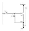
画素2はサンプリング用トランジスタT1と駆動用トランジスタT2と保持容量C1と発光素子ELとで構成されている。駆動用トランジスタT2はPチャネル型であり、その一方の電流端であるソースは電源ラインに接続し、他方の電流端であるドレインは発光素子ELに接続している。駆動用トランジスタT2の制御端であるゲートはサンプリング用トランジスタT1を介して信号線SLに接続している。サンプリング用トランジスタT1はライトスキャナ4から供給される制御信号に応じて導通し、信号線SLから供給される映像信号をサンプリングして保持容量C1に書き込む。駆動用トランジスタT2は保持容量C1に書き込まれた映像信号をゲート電圧Vgsとしてそのゲートに受け、ドレイン電流Idsを発光素子ELに流す。これにより発光素子ELは映像信号に応じた輝度で発光する。ゲート電圧Vgsは、ソースを基準にしたゲートの電位を表している。
The
駆動用トランジスタT2は飽和領域で動作し、ゲート電圧Vgsとドレイン電流Idsの関係は以下の特性式(1)で表される。
Ids=(1/2)μ(W/L)Cox(Vgs−Vth) 2 ・・・(1)
ここでμは駆動用トランジスタの移動度、Wは駆動用トランジスタのチャネル幅、Lは同じくチャネル長、Coxは同じく単位面積あたりのゲート絶縁膜容量、Vthは同じく閾電圧である。この特性式から明らかなように駆動用トランジスタT2は飽和領域で動作するとき、ゲート電圧Vgsに応じてドレイン電流Idsを供給する定電流源として機能する。
The driving transistor T2 operates in the saturation region, and the relationship between the gate voltage Vgs and the drain current Ids is expressed by the following characteristic equation (1).
Ids = (1/2) μ (W / L) Cox (Vgs−Vth) 2 (1 )
Here, μ is the mobility of the driving transistor, W is the channel width of the driving transistor, L is the channel length, Cox is the gate insulating film capacitance per unit area, and Vth is the threshold voltage. As is apparent from this characteristic equation, when the driving transistor T2 operates in the saturation region, it functions as a constant current source that supplies the drain current Ids according to the gate voltage Vgs.
図24は、発光素子ELの電圧/電流特性を示すグラフである。横軸にアノード電圧Vを示し、縦軸に駆動電流Idsをとってある。なお発光素子ELのアノード電圧は駆動用トランジスタT2のドレイン電圧となっている。発光素子ELは電流/電圧特性が経時変化し、特性カーブが時間の経過と共に寝ていく傾向にある。このため駆動電流Idsが一定であってもアノード電圧(ドレイン電圧)Vが変化してくる。その点、図23に示した画素回路2は駆動用トランジスタT2が飽和領域で動作し、ドレイン電圧の変動に関わらずゲートで電圧Vgsに応じた駆動電流Idsを流すことができるので、発光素子ELの特性経時変化に関わらず発光輝度を一定に保つことが可能である。
FIG. 24 is a graph showing voltage / current characteristics of the light emitting element EL. The horizontal axis represents the anode voltage V, and the vertical axis represents the drive current Ids. The anode voltage of the light emitting element EL is the drain voltage of the driving transistor T2. In the light emitting element EL, the current / voltage characteristics change with time, and the characteristic curve tends to fall with time. For this reason, the anode voltage (drain voltage) V changes even if the drive current Ids is constant. In that respect, the
図25は、従来の画素回路の他の例を示す回路図である。先に示した図23の画素回路と異なる点は、駆動用トランジスタT2がPチャネル型からNチャネル型に変わっていることである。回路の製造プロセス上は、画素を構成する全てのトランジスタをNチャネル型にすることが有利である場合が多い。 FIG. 25 is a circuit diagram showing another example of a conventional pixel circuit. A difference from the pixel circuit shown in FIG. 23 is that the driving transistor T2 is changed from the P-channel type to the N-channel type. In the circuit manufacturing process, it is often advantageous to make all the transistors constituting the pixel N-channel type.
表示パネルの高精細化及び大型化が進み、走査線の本数が1000本を越えてきている。多数本の走査線を線順次走査するライトスキャナも大型化してきている。近年は、表示パネル及び駆動部の大型化に伴い、いわゆるブロック駆動が開発されている。この場合、表示装置の駆動部は、所定本数ごとに走査線を区分してブロック化し、行列状の画素をブロック単位で順次駆動するブロック順次駆動と、各ブロック内で各走査線を走査して画素を行単位で順次駆動する線順次駆動とを行い、パネルに画像を表示している。 The display panel has been increased in definition and size, and the number of scanning lines has exceeded 1,000. A light scanner that scans a large number of scanning lines line-sequentially has also been increased in size. In recent years, so-called block driving has been developed along with the increase in the size of the display panel and the driving unit. In this case, the drive unit of the display device divides the scanning lines into blocks for each predetermined number, blocks sequential driving for sequentially driving the matrix pixels in units of blocks, and scans the scanning lines within each block. Line sequential driving for sequentially driving the pixels in units of rows is performed, and an image is displayed on the panel.
従来のブロック駆動では、隣り合うブロックの境界に位置する画素行の間で、動作条件の違いにより輝度の差が生じ、画面の均一性を損なうという問題があった。先後一対のブロックで、先行するブロックの最後の画素行は、そのブロックで最後に線順次走査される。一方後行のブロックの最初の画素行は、最初に線順次走査される。先行ブロックの最終行画素と、後行ブロックの先頭画素行は、互いに隣接しているにもかかわらず、駆動条件から見ると、線順次走査の順番が最後と最初となり、時間的な駆動条件が極端に相違しており、これが両画素行間の微妙な輝度の相違となって現われ、画面の均一性が低下する原因となっている。 In the conventional block drive, there is a problem that a luminance difference occurs due to a difference in operating conditions between pixel rows located at the boundary between adjacent blocks, and the uniformity of the screen is impaired. In the pair of blocks, the last pixel row of the preceding block is scanned line-sequentially at that block. On the other hand, the first pixel row of the succeeding block is first line-sequentially scanned. Although the last row pixel of the preceding block and the first pixel row of the succeeding block are adjacent to each other, when viewed from the driving conditions, the order of line sequential scanning is the last and first, and the temporal driving conditions are This is extremely different, and this appears as a subtle difference in luminance between the two pixel rows, which causes a reduction in the uniformity of the screen.
上述した従来の技術の課題に鑑み、本発明はブロック駆動方式の表示装置で画面の均一性を改善することを目的とする。かかる目的を達成するために以下の手段を講じた。即ち本発明は、行状に配された走査線と、列状に配された信号線と、各走査線と各信号線とが交差する部分に配された行列状の画素とを備えた画素アレイ部と、該走査線及び信号線を介して各画素を駆動する駆動部とからなる表示装置において、前記駆動部は、所定本数ごとに走査線を区分してブロック化し、行列状の画素をブロック単位で順次駆動するブロック順次駆動と、各ブロック内で、各走査線を走査して画素を行単位で順次駆動する線順次駆動とを行う。特徴事項として、隣り合うブロック間で、該線順次駆動の走査方向が互いに逆になる様に制御する。 In view of the above-described problems of the conventional technology, an object of the present invention is to improve screen uniformity in a block drive type display device. In order to achieve this purpose, the following measures were taken. That is, the present invention relates to a pixel array including scanning lines arranged in rows, signal lines arranged in columns, and matrix-like pixels arranged in a portion where each scanning line and each signal line intersect. And a drive unit that drives each pixel via the scan line and the signal line, the drive unit divides the scan line into blocks for each predetermined number, and blocks matrix pixels Block sequential driving for sequentially driving in units and line sequential driving for scanning each scanning line and sequentially driving pixels in units of rows in each block are performed. As a feature, control is performed so that the scanning directions of the line-sequential driving are reversed between adjacent blocks.
一態様では、前記駆動部は、列状の信号線に階調に応じた信号電位と所定の基準電位を有する映像信号を供給する信号セレクタと、行状の走査線に順次制御信号を供給するライトスキャナと、各走査線と平行に配された給電線に高電位と低電位で切り換わる電源電圧を供給するドライブスキャナとを有し、前記画素は、一方の電流端が信号線に接続し制御端が走査線に接続したサンプリング用トランジスタと、ドレイン側となる電流端が給電線に接続しゲートとなる制御端が該サンプリング用トランジスタの他方の電流端に接続した駆動用トランジスタと、該駆動用トランジスタのソース側となる電流端に接続した発光素子と、該駆動用トランジスタのソースとゲートとの間に接続した保持容量とを有し、前記ドライブスキャナは、行状の給電線を所定本数づつまとめてブロック化し、ブロック単位で順に位相をずらして高電位と低電位を切換えてブロック順次駆動を行い、且つブロック内では同じ位相で所定本数の給電線の電位を切り換え、前記ライトスキャナは、各ブロック内で水平周期ごとに順次各走査線に制御信号を供給する線順次駆動を行い、且つ隣り合うブロック間で該線順次駆動の走査方向を互いに逆になる様に制御する。好ましくは、前記電源スキャナは、ブロック順次駆動において、各給電線を一斉に高電位から低電位に切り換えて該駆動用トランジスタのソース電圧を下げた後各給電線を一斉に低電位から高電位に戻す補正準備動作を行う一方、前記ライトスキャナは、線順次駆動において、前記信号線が基準電位の時、各走査線に制御信号を供給し該サンプリング用トランジスタをオンして該駆動用トランジスタのソース電圧を上げ、駆動用トランジスタのゲートとソース間の電圧がその閾電圧に向うように該保持容量を放電する補正動作を行う。又、前記ライトスキャナは、線順次駆動において、前記信号線が信号電位の時、各走査線に制御信号を供給し該サンプリング用トランジスタをオンして信号電位を該保持容量に書き込む書込動作を行い、前記信号セレクタは、隣り合うブロック間で、各信号線に供給する信号電位の順番を互いに逆にする。又、前記電源スキャナは、各ブロックに対応して分割した複数のゲートドライバからなる。 In one aspect, the driving unit includes a signal selector that supplies a video signal having a signal potential corresponding to a gradation and a predetermined reference potential to a columnar signal line, and a light that sequentially supplies a control signal to the row scanning line. A scanner and a drive scanner for supplying a power supply voltage that switches between a high potential and a low potential to a power supply line arranged in parallel with each scanning line, and the pixel has one current terminal connected to a signal line and controlled A sampling transistor whose end is connected to the scanning line, a driving transistor whose drain-side current terminal is connected to the power supply line and whose gate is the control terminal is connected to the other current terminal of the sampling transistor, and the driving transistor A light emitting element connected to a current end on a source side of the transistor and a storage capacitor connected between a source and a gate of the driving transistor; A predetermined number of lines are grouped into blocks, the phase is shifted sequentially in block units, and the high potential and low potential are switched to perform block sequential driving, and the potential of a predetermined number of power supply lines is switched in the same phase within the block, The write scanner performs line-sequential driving for sequentially supplying a control signal to each scanning line for each horizontal period within each block, and controls the scanning direction of the line-sequential driving to be opposite to each other between adjacent blocks. . Preferably, in the block sequential driving, the power supply scanner simultaneously switches each power supply line from a high potential to a low potential to lower the source voltage of the driving transistor, and then simultaneously changes each power supply line from a low potential to a high potential. On the other hand, the write scanner supplies a control signal to each scanning line to turn on the sampling transistor and turn on the source of the driving transistor when the signal line is at the reference potential in line sequential driving. The voltage is increased, and a correction operation is performed to discharge the storage capacitor so that the voltage between the gate and the source of the driving transistor is directed to the threshold voltage. In the line-sequential drive, when the signal line is at a signal potential, the write scanner performs a writing operation of supplying a control signal to each scanning line, turning on the sampling transistor, and writing the signal potential to the storage capacitor. The signal selector reverses the order of signal potentials supplied to each signal line between adjacent blocks. The power scanner includes a plurality of gate drivers divided corresponding to each block.
他の態様では、各画素は少なくとも、サンプリング用トランジスタと、駆動用トランジスタと、保持容量と、発光素子とを備え、前記サンプリング用トランジスタは、その制御端が該走査線に接続し、その一対の電流端が該信号線と該駆動用トランジスタの制御端との間に接続し、前記駆動用トランジスタは、一対の電流端の一方が該発光素子に接続し、他方が電源に接続し、前記保持容量は、該駆動用トランジスタの制御端と電流端との間に接続し、前記駆動部は少なくとも、各走査線に制御信号を供給するライトスキャナと、各信号線に信号電位と基準電位とを切り換えて供給する信号セレクタとを有し、前記サンプリング用トランジスタは、該信号線が基準電位にある時該走査線に供給された制御信号に応じて閾電圧補正動作を行い、該駆動用トランジスタの閾電圧に相当する電圧を該保持容量に書き込むとともに、該信号線が信号電位にある時該走査線に供給された制御信号に応じて信号電位書込動作を行い、該信号線から信号電位をサンプリングして該保持容量に書き込み、前記駆動用トランジスタは、該保持容量に書き込まれた信号電位に応じた駆動電流を該発光素子に供給して発光させ、前記ライトスキャナは、所定本数ごとに走査線を区分してブロック化し、且つ所定本数の走査線の各々に割り当てられた走査期間を合成して、第1期間及び第2期間に分かれた一合成期間とし、前記ライトスキャナは、各ブロックを順次合成期間毎に選択して画素アレイ部をブロック順次駆動するとともに、各合成期間の該第1期間で、一ブロックに属する所定本数の走査線に一斉に制御信号を供給して、ブロック単位で閾電圧補正動作を実行し、該第2期間で、一ブロックに属する所定本数の走査線に順次制御信号を出力して線順次駆動を行い、以って画素の行毎に順次信号電位書込動作を実行し、隣り合うブロックで、各走査線に順次制御信号を出力して線順次駆動を行う走査方向を互いに逆にする。好ましくは、前記ライトスキャナは、各ブロックに対応して分割した複数のゲートドライバからなる。又隣り合うブロック間で互いに隣り合う行に属する画素は、閾電圧補正動作を完了してから信号電位書込動作に入るまでの時間が同一である。 In another aspect, each pixel includes at least a sampling transistor, a driving transistor, a storage capacitor, and a light emitting element, and the sampling transistor has a control end connected to the scanning line, A current end is connected between the signal line and a control end of the driving transistor, and the driving transistor has one of a pair of current ends connected to the light emitting element, the other connected to a power source, and the holding The capacitor is connected between the control terminal and the current terminal of the driving transistor, and the driving unit supplies at least a write scanner for supplying a control signal to each scanning line, and a signal potential and a reference potential for each signal line. A switching signal to be supplied, and the sampling transistor performs a threshold voltage correction operation according to a control signal supplied to the scanning line when the signal line is at a reference potential, A voltage corresponding to the threshold voltage of the driving transistor is written to the storage capacitor, and when the signal line is at the signal potential, a signal potential writing operation is performed in accordance with a control signal supplied to the scanning line, and the signal line The signal potential is sampled and written to the storage capacitor, and the driving transistor supplies the light emitting element with a driving current corresponding to the signal potential written to the storage capacitor to emit light. The scanning line is divided into blocks for each number, and the scanning period assigned to each of the predetermined number of scanning lines is combined into one combined period divided into a first period and a second period. In addition, each block is sequentially selected for each synthesis period to drive the pixel array block sequentially, and in the first period of each synthesis period, one block is assigned to a predetermined number of scanning lines belonging to one block. , A threshold voltage correction operation is executed for each block, and in the second period, a control signal is sequentially output to a predetermined number of scanning lines belonging to one block to perform line sequential driving. Then, the signal potential writing operation is sequentially executed for each row of pixels, and in the adjacent blocks, the control directions are sequentially output to the respective scanning lines to reverse the scanning directions in which the line sequential driving is performed. Preferably, the write scanner includes a plurality of gate drivers divided corresponding to each block. In addition, pixels belonging to adjacent rows between adjacent blocks have the same time from the completion of the threshold voltage correction operation to the start of the signal potential writing operation.
本発明によれば、隣り合うブロック間で、線順次駆動の走査方向が互いに逆になる様に制御している。これにより、隣り合うブロックの境界に位置する画素行の間で、動作条件の違いが最小となり、輝度の差が生じないので、画面の均一性を改善することができる。先後一対のブロックで、先行するブロックの最後の画素行は、そのブロックで最後に線順次走査される。一方後行のブロックの最初の画素行も、最後に線順次走査される。これは、隣り合うブロック間で、線順次駆動の走査方向が互いに逆になる様に制御しているからである。互いに隣接している先行ブロックの最終行画素と後行ブロックの先頭画素行は、ともに最後に線順次走査される行となり、時間的な駆動条件が同じになって両画素行間の輝度の相違は生じず、画面の均一性を改善することができる。 According to the present invention, control is performed so that the scanning directions of line sequential driving are opposite to each other between adjacent blocks. This minimizes the difference in operating conditions between pixel rows located at the boundary between adjacent blocks and does not cause a difference in luminance, so that the uniformity of the screen can be improved. In the pair of blocks, the last pixel row of the preceding block is scanned line-sequentially at that block. On the other hand, the first pixel row of the succeeding block is also scanned line-sequentially. This is because control is performed so that the scanning directions of line-sequential driving are opposite to each other between adjacent blocks. The last row pixel of the preceding block and the first pixel row of the succeeding block that are adjacent to each other are both row-sequentially scanned, and the temporal driving conditions are the same, and the difference in luminance between the two pixel rows is It does not occur and the uniformity of the screen can be improved.
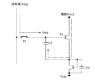
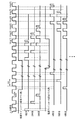
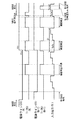
以下図面を参照して本発明の実施の形態を詳細に説明する。図1は本発明の表示装置の第1実施形態の全体構成を示すブロック図である。図示するように、本表示装置は、画素アレイ部1とこれを駆動する駆動部(3,4,5)とからなる。画素アレイ部1は、行状の走査線WSと、列状の信号線SLと、両者が交差する部分に配された行列状の画素2と、各画素2の各行に対応して配された電源ラインである給電線DSとを備えている。駆動部(3,4,5)は、各走査線WSに順次制御信号を供給して画素2を行単位で線順次走査する制御用スキャナ(ライトスキャナ)4と、この線順次走査に合わせて各給電線DSに高電位と低電位で切換る電源電圧を供給する電源スキャナ(ドライブスキャナ)5と、この線順次走査に合わせて列状の信号線SLに映像信号となる信号電位と基準電位を供給する信号セレクタ(水平セレクタ)3とを備えている。なおライトスキャナ4は外部から供給されるクロック信号WSckに応じて動作し同じく外部から供給されるスタートパルスWSspを順次転送することで、各走査線WSに制御信号を出力している。ドライブスキャナ5は外部から供給されるクロック信号DSckに応じて動作し、同じく外部から供給されるスタートパルスDSspを順次転送することで、給電線DSの電位を線順次で切換えている。
Hereinafter, embodiments of the present invention will be described in detail with reference to the drawings. FIG. 1 is a block diagram showing the overall configuration of the first embodiment of the display device of the present invention. As shown in the figure, the display device includes a
本第1実施形態では、ドライブスキャナ5は、行状の給電線DSを所定の本数ずつまとめてブロック化し、ブロック単位で順に位相をずらして高電位Vccと低電位Vssの切換を行い、且つブロック内では同じ位相で所定本数の給電線DSの電位を切換えている。図示の例では、ドライブスキャナ5は、行状の給電線DSを2本ずつまとめてブロック化し、ブロック単位で順に位相をずらして高電位と低電位の切換を行い、且つブロック内では同じ位相で2本の給電線DSの電位を切換えている。但し本発明はブロック化する本数が2本に限られるものではなく、一般的に複数行(複数段)で給電線(電源ライン)DSの駆動タイミングを共通化している。
In the first embodiment, the
ドライブスキャナ5は基本的にシフトレジスタとその各段ごとに接続した出力バッファとで構成されている。シフトレジスタは外部から供給されたクロック信号DSckに応じて動作し、同じく外部から供給されるスタート信号DSspを順次転送することで、各段ごとに電源切換えの元になる制御信号を出力している。出力バッファは、この制御信号に応じて電源ラインを高電位と低電位で切換え、給電線DSに供給している。本発明では、複数の電源ラインの制御タイミングを共通化することで、出力バッファを複数の電源ライン間で共用している。これにより、出力バッファの数を削減することができる。出力バッファは給電線DSに電源供給するため、大きな電流駆動能力が必要であり、そのデバイスサイズが大きい。このデバイスサイズの大きい出力バッファの個数を削減することで、周辺駆動部の回路サイズの縮小化、コストダウン、高歩留り化を図ることができる。例えば図1の例のように、1個の出力バッファを2個の給電線DSで共用すれば、全体として出力バッファの個数を第1実施形態に比べ半減できる。また10本の給電線DSの制御タイミングを共通化すれば、出力バッファの個数を第1実施形態の10分の1にすることが可能である。
The
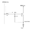
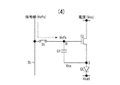
図2は、図1に示した表示装置に含まれる画素2の具体的な構成を示す回路図である。図示するように本画素回路2は、有機ELデバイスなどで代表される2端子型(ダイオード型)の発光素子ELと、Nチャネル型のサンプリング用トランジスタT1と、同じくNチャネル型の駆動用トランジスタT2と、薄膜タイプの保持容量C1とで構成されている。サンプリング用トランジスタT1はその制御端であるゲートが走査線WSに接続し、その一対の電流端であるソース及びドレインの一方が信号線SLに接続し、他方が駆動用トランジスタT2のゲートGに接続している。駆動用トランジスタT2は、そのソース及びドレインの一方が発光素子ELに接続し、他方が給電線DSに接続している。本形態は駆動用トランジスタT2がNチャネル型であり、その片方の電流端であるドレイン側が給電線DSに接続し、もう片方の電流端であるソースS側が発光素子ELのアノード側に接続している。発光素子ELのカソードは所定のカソード電位Vcatに固定されている。保持容量C1は駆動用トランジスタT2の電流端であるソースSと制御端であるゲートGとの間に接続している。かかる構成を有する画素2に対して、制御用スキャナ(ライトスキャナ)4は、走査線WSを低電位と高電位の間で切り換えることで順次制御信号を出力し、画素2を行単位で線順次走査する。電源スキャナ(ドライブスキャナ)5は、線順次走査に合わせて各給電線DSに高電位Vccと低電位Vssで切換る電源電圧を供給している。信号セレクタ(水平セレクタ3)は、線順次走査に合わせて列状の信号線SLに映像信号となる信号電位Vsigと基準電位Vofsを供給している。
FIG. 2 is a circuit diagram showing a specific configuration of the
かかる構成において、給電線DSが高電位Vccであり且つ信号線SLがVofsのときに、サンプリング用トランジスタT1が制御信号に応じてオンすることで発光素子ELを点灯状態から消灯状態に切換える消灯動作を行う。続いて給電線DSを高電位Vccから低電位Vssに切換えると共に、給電線DSが低電位Vssにある間はサンプリング用トランジスタT1をオンせずに、駆動用トランジスタT2のソース電圧を下げ、ゲートG・ソースS間電圧Vgsを駆動用トランジスタT2の閾電圧Vthを超える電圧にセットするための準備動作を行う。この後給電線DSを低電位Vssから高電位Vccに戻し且つ信号線SLが基準電位Vofsのとき、サンプリング用トランジスタT1が制御信号に応じてオンして駆動用トランジスタT2のソース電圧を上げ、ゲートG・ソースS間電圧Vgsがその閾電圧Vthに向かうように保持容量C1を放電する補正動作を行う。 In such a configuration, when the power supply line DS is at the high potential Vcc and the signal line SL is Vofs, the light-emitting element EL is switched from the light-on state to the light-off state by turning on the sampling transistor T1 according to the control signal. I do. Subsequently, the feed line DS is switched from the high potential Vcc to the low potential Vss, and while the feed line DS is at the low potential Vss, the sampling transistor T1 is not turned on, the source voltage of the drive transistor T2 is lowered, and the gate G A preparatory operation for setting the source-to-source voltage Vgs to a voltage exceeding the threshold voltage Vth of the driving transistor T2 is performed. Thereafter, when the power supply line DS is returned from the low potential Vss to the high potential Vcc and the signal line SL is at the reference potential Vofs, the sampling transistor T1 is turned on according to the control signal to increase the source voltage of the driving transistor T2, and the gate A correction operation for discharging the storage capacitor C1 is performed so that the G-source S voltage Vgs is directed toward the threshold voltage Vth.
本発明によれば、まず始めに、給電線DSが高電位Vccで且つ信号線SLが基準電位Vofsのときに、発光素子ELを点灯状態から消灯状態に切換える消灯動作を行っている。続いて給電線DSを低電位Vssに切換えると共に、給電線DSが低電位Vssにある間サンプリング用トランジスタT1をオンさせることなく、駆動用トランジスタT2のゲート・ソース間電圧Vgsをその閾電圧Vthより大きな電圧に設定するための準備動作を行っている。この後給電線DSを低電位Vssから高電位Vccに戻し且つ信号線SLが基準電位Vofsのときに、サンプリング用トランジスタT1をオンして駆動用トランジスタT2のゲート・ソース間電圧Vgsがその閾電圧Vthに向かうように保持容量C1を放電する補正動作を行っている。この様に、消灯動作、準備動作及び補正動作を順番に行うことにより、誤動作を防止して確実且つ安定的に駆動用トランジスタT2の閾電圧補正を行うことができる。特に準備動作ではサンプリング用トランジスタT1をオンすることなく、駆動用トランジスタT2のソース電圧を下げることで、画素2の誤動作を防ぐと共に補正動作の安定化を図っている。
According to the present invention, first, when the power supply line DS is at the high potential Vcc and the signal line SL is at the reference potential Vofs, the light-emitting element EL is switched off from the on state to the off state. Subsequently, the power supply line DS is switched to the low potential Vss, and the gate-source voltage Vgs of the driving transistor T2 is set to the threshold voltage Vth without turning on the sampling transistor T1 while the power supply line DS is at the low potential Vss. A preparatory operation for setting a large voltage is performed. Thereafter, when the power supply line DS is returned from the low potential Vss to the high potential Vcc and the signal line SL is at the reference potential Vofs, the sampling transistor T1 is turned on, and the gate-source voltage Vgs of the driving transistor T2 becomes the threshold voltage. A correction operation is performed to discharge the storage capacitor C1 toward Vth. In this manner, by performing the turn-off operation, the preparation operation, and the correction operation in order, the malfunction can be prevented and the threshold voltage of the driving transistor T2 can be corrected reliably and stably. In particular, in the preparatory operation, the source voltage of the driving transistor T2 is lowered without turning on the sampling transistor T1, thereby preventing malfunction of the
図3−1は、図2に示した第1実施形態の動作説明に供するタイミングチャートである。なお本タイミングチャートは、3段分の電源ラインを共通のタイミングで制御している。図3−1のタイミングチャートは、信号線に供給される映像信号(入力信号)、3本ずつブロック化された給電線(電源ライン)の電位変化、及び各行(各段)の走査線に印加される制御信号(制御パルス)を表している。まず入力信号は、1水平期間(1H)内で、信号電位Vsigと基準電位Vofsが交互に切換っている。電源ラインは、1〜3段目の電位変化が共通化されており、1〜3段同時に、高電位から低電位に切換り、その後高電位に復帰している。一方1段目の走査線は、入力信号がVofsで電源ラインが高電位Vccのとき、1発目の制御パルスが出力され、対応する行の画素は点灯状態から消灯状態に切換る。その後2〜4発目の制御パルスが連続で発生し、閾電圧補正動作が3回繰り返される。最後に5発目の制御パルスが発生し、信号電位Vsigの書き込み及び移動度補正が行われる。 FIG. 3A is a timing chart for explaining the operation of the first embodiment shown in FIG. In this timing chart, the power lines for three stages are controlled at a common timing. In the timing chart of FIG. 3A, the video signal (input signal) supplied to the signal line, the potential change of the power supply line (power supply line) blocked by three lines, and the scanning line of each row (each stage) are applied. Represents a control signal (control pulse). First, in the input signal, the signal potential Vsig and the reference potential Vofs are alternately switched within one horizontal period (1H). In the power supply line, the potential changes in the first to third stages are shared, and the first to third stages are simultaneously switched from the high potential to the low potential and then returned to the high potential. On the other hand, when the input signal is Vofs and the power supply line is at the high potential Vcc, the first-stage scanning line outputs the first control pulse, and the pixels in the corresponding row are switched from the lit state to the unlit state. Thereafter, the second to fourth control pulses are continuously generated, and the threshold voltage correcting operation is repeated three times. Finally, a fifth control pulse is generated, and writing of the signal potential Vsig and mobility correction are performed.
2段目の走査線に対しては、1段目と位相が1Hだけシフトして、1番目〜5番目の制御パルスが順次出力され、1段目と同様に消灯動作、閾電圧補正動作及び信号電位書き込み動作が行われる。3段目も同様に、2段目から1H位相がシフトして5個の制御パルスが順次出力され、消灯動作、時分割補正動作及び信号書き込み動作が行われる。 For the second-stage scanning line, the phase is shifted by 1H from the first stage, and the first to fifth control pulses are sequentially output, and the turn-off operation, threshold voltage correction operation, and A signal potential write operation is performed. Similarly, in the third stage, the 1H phase is shifted from the second stage, and five control pulses are sequentially output, and the light-off operation, the time division correction operation, and the signal writing operation are performed.
動作シーケンスが4段目〜6段目に進むと、ドライブスキャナは4段目〜6段目で共通化した電源ラインを、一旦高電位Vccから低電位Vssに切換え、その後Vccに戻す。この様にドライブスキャナは、1〜3段目とは位相をずらして4〜6段目の電源ラインの電位切換を行っている。これに対応して4段目〜6段目の各走査線に順次5連の制御パルスが印加され、1〜3段目と同様の動作が繰り返される。 When the operation sequence proceeds to the fourth to sixth stages, the drive scanner temporarily switches the power line shared by the fourth to sixth stages from the high potential Vcc to the low potential Vss, and then returns to Vcc. In this way, the drive scanner switches the potentials of the power lines of the fourth to sixth stages while shifting the phase from the first to third stages. Correspondingly, five consecutive control pulses are sequentially applied to the fourth to sixth scanning lines, and the same operation as in the first to third stages is repeated.
以上の説明から明らかな通り、本実施形態では3段分の電源ラインを共通のタイミングで電位制御している。この様にすることでドライブスキャナの出力数を減らすことができ(本実施例では1/3とできる)、低コスト化が可能である。 As is clear from the above description, in this embodiment, the potential of the power supply lines for three stages is controlled at a common timing. By doing so, the number of outputs of the drive scanner can be reduced (in this embodiment, 1/3), and the cost can be reduced.
なお本実施形態では、電源ラインをVssからVccに戻した後、1回目の閾電圧補正動作を開始するまでの時間が、1段目、2段目及び3段目では異なる構成になっている。前述したように、電源ラインをVccからVssに戻したとき、駆動用トランジスタに流れる電流が小さければ(駆動用トランジスタのVgsが小さければ)、ゲート電圧及びソース電圧がほとんど上昇せず、いずれの段でも正常に閾電圧補正動作を行うことができる。 In the present embodiment, after the power line is returned from Vss to Vcc, the time until the first threshold voltage correction operation is started is different in the first stage, the second stage, and the third stage. . As described above, when the power supply line is returned from Vcc to Vss, if the current flowing through the driving transistor is small (Vgs of the driving transistor is small), the gate voltage and the source voltage hardly increase, and any stage However, the threshold voltage correction operation can be normally performed.
図3−2は、図2に示した画素の動作説明に供する別のタイミングチャートである。このタイミングチャートは時間軸を共通にして、走査線WSの電位変化、給電線(電源ライン)DSの電位変化、信号線SLの電位変化を表してある。走査線WSの電位変化は制御信号を表し、サンプリング用トランジスタT1の開閉制御を行っている。給電線DSの電位変化は、電源電圧Vcc,Vssの切換えを表している。また信号線SLの電位変化は入力信号の信号電位Vsigと基準電位Vofsの切換えを表している。またこれらの電位変化と並行に、駆動用トランジスタT2のゲートG及びソースSの電位変化も表している。前述したようにゲートGとソースSの電位差がVgsである。 FIG. 3B is another timing chart for explaining the operation of the pixel shown in FIG. This timing chart shows a change in the potential of the scanning line WS, a change in the potential of the power supply line (power supply line) DS, and a change in the potential of the signal line SL with a common time axis. The potential change of the scanning line WS represents a control signal, and the opening / closing control of the sampling transistor T1 is performed. The change in the potential of the power supply line DS represents switching between the power supply voltages Vcc and Vss. Further, the potential change of the signal line SL represents switching between the signal potential Vsig of the input signal and the reference potential Vofs. In parallel with these potential changes, the potential changes of the gate G and the source S of the driving transistor T2 are also shown. As described above, the potential difference between the gate G and the source S is Vgs.
このタイミングチャートは画素の動作シーケンスに合わせて期間を(1)〜(11)のように便宜的に区切ってある。点灯期間(1)では、画素が発光状態にある。消灯期間(2)になると、画素は発光状態から非発光状態に切換る。続いて準備期間(3)〜(5)では、画素は駆動用トランジスタの閾電圧補正のための準備動作を行う。この後補正期間(6)で実際の閾電圧補正動作を行う。通常この補正期間(6)は待機期間(8)を間にして複数回繰り返されて、閾電圧補正動作が完了する。その後書込期間(9)で信号電位が保持容量C1に書き込まれると共に、駆動用トランジスタT1の移動度補正が行われる。最後に発光期間(11)に進み、画素は非発光状態から発光状態に切換る。なお図では説明の簡略化のため、1回の閾電圧補正期間(6)で補正動作を行う様にしている。 In this timing chart, the periods are divided as shown in (1) to (11) for convenience in accordance with the operation sequence of the pixels. In the lighting period (1), the pixel is in a light emitting state. In the extinguishing period (2), the pixel switches from the light emitting state to the non-light emitting state. Subsequently, in the preparation periods (3) to (5), the pixel performs a preparatory operation for correcting the threshold voltage of the driving transistor. Thereafter, an actual threshold voltage correction operation is performed in the correction period (6). Normally, this correction period (6) is repeated a plurality of times with the standby period (8) in between, and the threshold voltage correction operation is completed. Thereafter, in the writing period (9), the signal potential is written into the holding capacitor C1, and the mobility of the driving transistor T1 is corrected. Finally, in the light emission period (11), the pixel is switched from the non-light emitting state to the light emitting state. In the figure, for simplification of description, the correction operation is performed in one threshold voltage correction period (6).
この後、書込期間/移動度補正期間(9)に進む。ここで映像信号の信号電位VsigがVthに足し込まれる形で保持容量C1に書き込まれると共に、移動度補正用の電圧ΔVが保持容量C1に保持された電圧から差し引かれる。この書込期間/移動度補正期間(9)では、信号線SLが信号電位Vsigにある時間帯にサンプリング用トランジスタT1を導通状態にする必要がある。この後発光期間(11)に進み、信号電位Vsigに応じた輝度で発光素子が発光する。その際信号電位Vsigは閾電圧Vthに相当する電圧と移動度補正用の電圧ΔVとによって調整されているため、発光素子ELの発光輝度は駆動用トランジスタT2の閾電圧Vthや移動度μのばらつきの影響を受けることはない。なお発光期間(11)の最初でブートストラップ動作が行われ、駆動用トランジスタT2のゲートG/ソースS間電圧Vgsを一定に維持したまま、駆動用トランジスタT2のゲート電位及びソース電位が上昇する。 Thereafter, the process proceeds to the writing period / mobility correction period (9). Here, the signal potential Vsig of the video signal is written into the storage capacitor C1 in a form added to Vth, and the mobility correction voltage ΔV is subtracted from the voltage held in the storage capacitor C1. In the writing period / mobility correction period (9), the sampling transistor T1 needs to be turned on in a time zone in which the signal line SL is at the signal potential Vsig. Thereafter, the process proceeds to the light emission period (11), and the light emitting element emits light with a luminance corresponding to the signal potential Vsig. At that time, since the signal potential Vsig is adjusted by a voltage corresponding to the threshold voltage Vth and the mobility correction voltage ΔV, the light emission luminance of the light emitting element EL varies in the threshold voltage Vth and mobility μ of the driving transistor T2. Will not be affected. Note that the bootstrap operation is performed at the beginning of the light emission period (11), and the gate potential and the source potential of the driving transistor T2 rise while the gate G / source S voltage Vgs of the driving transistor T2 is kept constant.
引き続き図4−1〜図4−11を参照して、図2に示した画素回路の動作を詳細に説明する。まず、発光素子ELの発光期間(1)は図4−1のように電源がVccであり、サンプリング用トランジスタT1がオフした状態である。この時駆動用トランジスタT2は飽和領域で動作するように設定されているため、発光素子ELに流れる電流Idsは駆動用トランジスタT2のゲートソース間電圧Vgsに応じて特性式1に示される値をとる。
The operation of the pixel circuit shown in FIG. 2 will be described in detail with reference to FIGS. First, in the light emission period (1) of the light emitting element EL, the power source is Vcc as shown in FIG. 4A and the sampling transistor T1 is turned off. At this time, since the driving transistor T2 is set to operate in the saturation region, the current Ids flowing through the light emitting element EL takes a value represented by the
次に消灯期間(2)において、信号線電位がVofsの時にサンプリング用トランジスタT1をオンして駆動用トランジスタT2のゲートにVofsを入力する(図4−2)。これにより駆動用トランジスタT2のゲートソース間電圧は閾電圧以下となり、発光素子ELに電流が流れなくなるため発光素子ELは消灯する。その時発光素子ELにかかる電圧は発光素子ELの閾電圧となるため、発光素子ELのアノード電圧は発光素子ELの閾電圧とカソード電圧の和、つまりVcat+Vthelとなる。 Next, in the extinguishing period (2), when the signal line potential is Vofs, the sampling transistor T1 is turned on and Vofs is input to the gate of the driving transistor T2 (FIG. 4-2). As a result, the gate-source voltage of the driving transistor T2 becomes equal to or lower than the threshold voltage, and no current flows through the light emitting element EL, so that the light emitting element EL is turned off. At that time, since the voltage applied to the light emitting element EL becomes the threshold voltage of the light emitting element EL, the anode voltage of the light emitting element EL becomes the sum of the threshold voltage and the cathode voltage of the light emitting element EL, that is, Vcat + Vthel.
さらに一定時間経過後、準備期間(3)で、電源電圧をVccからVssへと変化させる。この時、電源側が駆動用トランジスタT2のソースとなり、図4−3のように発光素子ELのアノードから電源へ電流が流れる。これにより発光素子ELのアノードの電圧は時間とともに低下してゆく。この時、サンプリング用トランジスタT1はオフしているため駆動用トランジスタT2のゲートも発光素子ELのアノード電圧とともに低下する。つまり時間とともに駆動用トランジスタT2のゲートソース間電圧(駆動用トランジスタT2のゲートと電源間電位)が小さくなってゆく。 Further, after a predetermined time has elapsed, the power supply voltage is changed from Vcc to Vss in the preparation period (3). At this time, the power source side becomes the source of the driving transistor T2, and a current flows from the anode of the light emitting element EL to the power source as shown in FIG. 4-3. Thereby, the voltage of the anode of the light emitting element EL decreases with time. At this time, since the sampling transistor T1 is off, the gate of the driving transistor T2 also decreases with the anode voltage of the light emitting element EL. That is, the gate-source voltage of the driving transistor T2 (the potential between the gate of the driving transistor T2 and the power source) decreases with time.
この時、駆動用トランジスタT2が飽和領域で動作するなら、つまり、Vgs−Vthd≦Vdsであるなら、期間(4)で図4−4に示すように駆動用トランジスタT2のゲートはVss+Vthdとなる。ここでVthdは駆動用トランジスタT2のゲート電源間の閾電圧である。 At this time, if the driving transistor T2 operates in the saturation region, that is, if Vgs−Vthd ≦ Vds, the gate of the driving transistor T2 becomes Vss + Vthd as shown in FIG. Here, Vthd is a threshold voltage between the gate power supplies of the driving transistor T2.
期間(5)で電源電圧を再びVccとする(図4−5)。この時駆動用トランジスタT2のゲートに入力されるカップリング量をΔV、発光素子ELのアノード電圧をVxとしている。電源をVccとすることで駆動用トランジスタT2のソースは発光素子ELのアノードとなり、駆動用トランジスタT2のゲートソース間電圧Vgsによって電源から発光素子ELのアノードへ電流が流れるが、駆動用トランジスタT2のゲートソース間電圧が閾電圧よりも小さければ電流によるゲート、ソースはほとんど上昇しない。 In the period (5), the power supply voltage is again set to Vcc (FIG. 4-5). At this time, the coupling amount input to the gate of the driving transistor T2 is ΔV, and the anode voltage of the light emitting element EL is Vx. By setting the power supply to Vcc, the source of the driving transistor T2 becomes the anode of the light emitting element EL, and a current flows from the power supply to the anode of the light emitting element EL by the gate-source voltage Vgs of the driving transistor T2. If the gate-source voltage is smaller than the threshold voltage, the gate and source due to current hardly rise.
そして閾値補正期間(6)において信号電圧がVofsの時にサンプリング用トランジスタT1をオンする(図4−6)。これにより駆動用トランジスタT2のゲート電圧はVofsとなり、ゲート電圧の変化量が保持容量C1、ゲートソース間の寄生容量Cgs、発光素子ELの寄生容量Celによる一定比でソースに入力される。この時の入力比をgとする。gは以下の式2で示される値である。
g=(C1+Cgs)/(C1+Cgs+Cel) (2)
In the threshold correction period (6), the sampling transistor T1 is turned on when the signal voltage is Vofs (FIG. 4-6). As a result, the gate voltage of the driving transistor T2 becomes Vofs, and the amount of change in the gate voltage is input to the source at a constant ratio by the holding capacitor C1, the parasitic capacitance Cgs between the gate and the source, and the parasitic capacitance Cel of the light emitting element EL. The input ratio at this time is represented by g. g is a value represented by the following
g = (C1 + Cgs) / (C1 + Cgs + Cel) (2)
この状態で駆動用トランジスタT2のゲートソース間電圧Vgsがその閾電圧Vthよりも大きければ図4−6に示すように電源から電流が流れる。換言すればこの時のVgsが駆動用トランジスタT2の閾電圧よりも大きくなるようにVofs、Vssの値を設定する必要がある。前述の通り発光素子ELの等価回路はダイオードと容量で表されるため、Vel≦Vcat+Vthel(発光素子ELのリーク電流が駆動用トランジスタT2に流れる電流よりもかなり小さい)である限り、駆動用トランジスタT2の電流はC1とCelを充電するために使われる。この時、Velは時間と共に図4−7のように上昇してゆく。 In this state, if the gate-source voltage Vgs of the driving transistor T2 is larger than the threshold voltage Vth, a current flows from the power supply as shown in FIG. In other words, it is necessary to set the values of Vofs and Vss so that Vgs at this time is larger than the threshold voltage of the driving transistor T2. As described above, since the equivalent circuit of the light emitting element EL is represented by a diode and a capacitor, as long as Vel ≦ Vcat + Vthel (the leakage current of the light emitting element EL is considerably smaller than the current flowing through the driving transistor T2), the driving transistor T2 Current is used to charge C1 and Cel. At this time, Vel rises with time as shown in FIG. 4-7.
次の待機期間(8)では、信号電圧がVofsからVsigに変わる前にサンプリング用トランジスタT1をオフする。この時、駆動用トランジスタT2のゲートソース間電圧はVthよりも大きいため、図4−8のように電流が流れ、駆動用トランジスタT2のゲート、ソース電圧は上昇してゆく。この時、発光素子ELには逆バイアスがかかっているため発光素子ELが発光することはない。 In the next standby period (8), the sampling transistor T1 is turned off before the signal voltage changes from Vofs to Vsig. At this time, since the gate-source voltage of the driving transistor T2 is larger than Vth, a current flows as shown in FIG. 4-8, and the gate and source voltages of the driving transistor T2 rise. At this time, since the reverse bias is applied to the light emitting element EL, the light emitting element EL does not emit light.
閾値キャンセル動作終了後サンプリング用トランジスタT1をオフする。続いて書込期間(9)で信号線電位がVsigとなった時、サンプリング用トランジスタT1を再度オンする(図4−9)。Vsigは階調に応じた電圧である。駆動用トランジスタT2のゲート電位はサンプリング用トランジスタT1をオンしているためにVsigとなるが、電源から電流が流れるためソース電位は時間とともに上昇してゆく。この時駆動用トランジスタT2のソース電圧が発光素子ELの閾電圧Vthelとカソード電圧Vcatの和を越えなければ(発光素子ELのリーク電流が駆動用トランジスタT2に流れる電流よりもかなり小さければ)駆動用トランジスタT2の電流はC1とCelを充電するのに使用される。この時駆動用トランジスタT2の閾値補正動作は完了しているため、駆動用トランジスタT2が流す電流は移動度μを反映したものとなる。具体的にいうと移動度が大きいものはこの時の電流量が大きく、ソースの上昇も早い。逆に移動度が小さいものは電流量が小さく、ソースの上昇は遅くなる(図4−10)。これによって駆動用トランジスタT2のゲートソース間電圧は移動度を反映して小さくなり一定時間経過後に完全に移動度を補正するVgsとなる。 After completion of the threshold cancel operation, the sampling transistor T1 is turned off. Subsequently, when the signal line potential becomes Vsig in the writing period (9), the sampling transistor T1 is turned on again (FIG. 4-9). Vsig is a voltage corresponding to the gradation. The gate potential of the driving transistor T2 becomes Vsig because the sampling transistor T1 is turned on, but since the current flows from the power supply, the source potential increases with time. At this time, if the source voltage of the driving transistor T2 does not exceed the sum of the threshold voltage Vthel and the cathode voltage Vcat of the light emitting element EL (if the leakage current of the light emitting element EL is much smaller than the current flowing through the driving transistor T2), The current in transistor T2 is used to charge C1 and Cel. At this time, since the threshold value correcting operation of the driving transistor T2 is completed, the current flowing through the driving transistor T2 reflects the mobility μ. Specifically, those with high mobility have a large current amount at this time, and the source rises quickly. On the other hand, when the mobility is low, the amount of current is small and the source rises slowly (FIG. 4-10). As a result, the gate-source voltage of the driving transistor T2 is reduced to reflect the mobility, and becomes Vgs for completely correcting the mobility after a predetermined time has elapsed.
最後にサンプリング用トランジスタT1をオフして書き込みが終了し発光期間(11)になると、発光素子ELを発光させる。駆動用トランジスタT2のゲートソース間電圧は一定であるので駆動用トランジスタT2は一定電流Ids’を発光素子ELに流し、Velは発光素子ELにIds’という電流が流れる電圧まで上昇し、発光素子ELは発光する(図4−11) Finally, when the sampling transistor T1 is turned off and writing is completed and the light emission period (11) is reached, the light emitting element EL is caused to emit light. Since the gate-source voltage of the driving transistor T2 is constant, the driving transistor T2 passes a constant current Ids ′ to the light emitting element EL, and Vel rises to a voltage at which a current of Ids ′ flows through the light emitting element EL. Emits light (Figure 4-11)
本回路においても発光素子ELは発光時間が長くなるとそのI−V特性は変化してしまう。そのため図中B点の電位も変化する。しかしながら、駆動用トランジスタT2のゲートソース間電圧は一定値に保たれているので発光素子ELに流れる電流は変化しない。よって発光素子ELのI−V特性が劣化しても、一定電流Idsが常に流れ続け、発光素子ELの輝度が変化することはない。 In this circuit as well, the IV characteristic of the light emitting element EL changes as the light emission time becomes longer. Therefore, the potential at point B in the figure also changes. However, since the gate-source voltage of the driving transistor T2 is kept constant, the current flowing through the light emitting element EL does not change. Therefore, even if the IV characteristic of the light emitting element EL deteriorates, the constant current Ids always flows, and the luminance of the light emitting element EL does not change.
ここで本画素回路の駆動について考える。本駆動は前述の通り図3−1に示す駆動タイミングをとるが、電源ラインをVssからVccへ変化させた後、閾値補正動作を行うまでの時間が電源ラインのタイミングを共通にしているライン間で異なる。具体的にはN段目よりもN+1段目の方が閾値補正を行うまでに電源ラインがVccという電位にいる時間が長い。これにより駆動用トランジスタのリーク電流、発光素子のリーク電流によって駆動用トランジスタのソース電圧はN段目よりもN+1段目の方が上昇する。 Here, driving of the pixel circuit is considered. As described above, the main drive takes the drive timing shown in FIG. 3A. However, after the power supply line is changed from Vss to Vcc, the time until the threshold correction operation is performed is between the lines having the same power supply line timing. It is different. Specifically, the time for which the power supply line is at the potential Vcc is longer before the threshold correction is performed in the (N + 1) th stage than in the Nth stage. Accordingly, the source voltage of the driving transistor is higher in the (N + 1) th stage than in the Nth stage due to the leakage current of the driving transistor and the leakage current of the light emitting element.
基本的に閾値補正動作前に駆動用トランジスタのソース電圧が異なっても閾値補正動作において駆動用トランジスタのゲートソース間電圧Vgsがその閾値電圧Vthよりも大きければ正常に閾値補正動作を行うことができる。しかしながら、発光輝度は閾値補正動作前における駆動用トランジスタのソース電圧に依存する。このため、本駆動では電源ラインのタイミングを共通化している最終段と次の段で(図3−1では3段目と4段目)閾値補正を行う際の駆動用トランジスタのソース電圧が急激に変化してしまう(1段目から3段目は緩やかに変化する)。 Basically, even if the source voltage of the driving transistor is different before the threshold correction operation, the threshold correction operation can be normally performed if the gate-source voltage Vgs of the driving transistor is larger than the threshold voltage Vth in the threshold correction operation. . However, the light emission luminance depends on the source voltage of the driving transistor before the threshold correction operation. For this reason, in this driving, the source voltage of the driving transistor at the time of threshold correction at the last stage and the next stage (the third stage and the fourth stage in FIG. (From the first stage to the third stage changes slowly).
このため、表示装置の画面には、図5のように電源タイミングを共通化している複数のライン(以下、ブロックと呼ぶ)の周期でスジのようなムラが発生してしまう。なお、図ではムラを実際より誇張して表している。 For this reason, streaks such as streaks occur on the screen of the display device at the cycle of a plurality of lines (hereinafter referred to as blocks) sharing the power supply timing as shown in FIG. In the figure, the unevenness is exaggerated from the actual value.
本発明では上記問題点を対策するためにブロック内におけるサンプリング用トランジスタの走査方向を隣接するブロック間で逆転させることを提案する。図6に一例として本発明を適用した場合のタイミングを示す。このタイミングチャートは基本的に図3−1と同じである。本発明において図3−1の場合と異なる点は、電源電圧をVssからVccとしてから閾値補正動作を行うまでの時間が隣接するブロック間の隣接ラインで同じとなっている点と、画素に入力される信号電圧の出力順が隣接ブロック間で逆となっている点である。 The present invention proposes to reverse the scanning direction of the sampling transistor in the block between adjacent blocks in order to solve the above-mentioned problems. FIG. 6 shows the timing when the present invention is applied as an example. This timing chart is basically the same as FIG. In the present invention, the difference from the case of FIG. 3A is that the time from when the power supply voltage is changed from Vss to Vcc until the threshold correction operation is performed is the same in adjacent lines between adjacent blocks, and input to the pixels. The output order of the signal voltage is reversed between adjacent blocks.
本発明を用いることで隣接するブロック間の隣接ライン間で電源ラインをVccとしてから閾値補正動作を行うまでの時間を同じとすることができ、駆動用トランジスタや発光素子ELのリーク電流になどによる駆動用トランジスタのソース電圧の上昇量を同じとすることができる。その結果、対策前では図5のように視認されるブロック間のスジムラを図7のようなシェーディングのようなムラに置き換えることができる。なお図5,7ではシェーディングムラを実際より誇張して表している。一般的に隣接ブロック間で急激に変わるスジのようなムラは1%程度の輝度差で視認されてしまうが、シェーディングのように緩やかに変化するムラは1%程度の輝度差では視認できないため、本発明を用いることでムラが視認されない均一な画質を得ることができる。また、本発明を用いることでブロックを構成するライン数を増やしてもムラが視認されないため、従来に比べてブロックを構成するライン数を増やすことが、つまりパネルのブロック数を減らすことができ、低コスト化が実現可能となっている。また、本発明はサンプリング用トランジスタのスキャン方向を隣接ブロック毎に反転する方式をとるため、ゲートドライバを内蔵しないパネルの場合、ユニットはゲートドライバ単位であることが望ましい。 By using the present invention, the time from when the power supply line is set to Vcc to the threshold correction operation between adjacent lines between adjacent blocks can be made the same, depending on the leakage current of the driving transistor and the light emitting element EL, etc. The amount of increase in the source voltage of the driving transistor can be made the same. As a result, it is possible to replace the uneven stripe between the blocks visually recognized as shown in FIG. 5 with unevenness such as shading as shown in FIG. 5 and 7, the shading unevenness is exaggerated from the actual value. Generally, unevenness such as streaks that change suddenly between adjacent blocks is visually recognized with a luminance difference of about 1%, but unevenness that changes slowly like shading cannot be visually recognized with a luminance difference of about 1%. By using the present invention, uniform image quality in which unevenness is not visually recognized can be obtained. In addition, even if the number of lines constituting the block is increased by using the present invention, unevenness is not visually recognized, so that the number of lines constituting the block can be increased compared to the conventional case, that is, the number of blocks of the panel can be reduced. Cost reduction is possible. In addition, since the present invention adopts a method in which the scanning direction of the sampling transistor is inverted for each adjacent block, in the case of a panel without a built-in gate driver, the unit is preferably a gate driver unit.
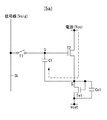
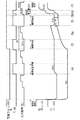
図8−1は本発明にかかる表示装置の第2実施形態の全体構成を示すブロック図である。図示するように、本表示装置は、画素アレイ部1とこれを駆動する駆動部(3,4,5)とからなる。画素アレイ部1は、行状の走査線WSと、列状の信号線SLと、両者が交差する部分に配された行列状の画素2と、各画素2の各行に対応して配された電源ラインである給電線DSとを備えている。駆動部(3,4,5)は、各走査線WSに順次制御信号を供給して画素2を行単位で線順次走査する制御用スキャナ(ライトスキャナ)4と、この線順次走査に合わせて各給電線DSに第1電位と第2電位で切換る電源電圧を供給する電源スキャナ(ドライブスキャナ)5と、この線順次走査に合わせて列状の信号線SLに映像信号となる信号電位と基準電位を供給する信号ドライバ(水平セレクタ)3とを備えている。なおライトスキャナ4は外部から供給されるクロック信号WSckに応じて動作し同じく外部から供給されるスタートパルスWSspを順次転送することで、各走査線WSに制御信号を出力している。ドライブスキャナ5は外部から供給されるクロック信号DSckに応じて動作し、同じく外部から供給されるスタートパルスDSspを順次転送することで、給電線DSの電位を線順次で切換えている。図1に示した第1実施形態と異なる点は、給電線DSがブロック単位で共通化されていないことである。
FIG. 8A is a block diagram showing the overall configuration of the second embodiment of the display device according to the present invention. As shown in the figure, the display device includes a
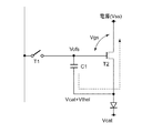
図8−2は、図8−1に示した表示装置に含まれる画素2の具体的な構成を示す回路図である。図示するように本画素回路2は、有機ELデバイスなどで代表される2端子型(ダイオード型)の発光素子ELと、Nチャネル型のサンプリング用トランジスタT1と、同じくNチャネル型の駆動用トランジスタT2と、薄膜タイプの保持容量C1とで構成されている。サンプリング用トランジスタT1はその制御端であるゲートが走査線WSに接続し、その一対の電流端であるソース及びドレインの一方が信号線SLに接続し、他方が駆動用トランジスタT2のゲートGに接続している。駆動用トランジスタT2は、そのソース及びドレインの一方が発光素子ELに接続し、他方が給電線DSに接続している。本形態は駆動用トランジスタT2がNチャネル型であり、その片方の電流端であるドレイン側が給電線DSに接続し、もう片方の電流端であるソースS側が発光素子ELのアノード側に接続している。発光素子ELのカソードは所定のカソード電位Vcatに固定されている。保持容量C1は駆動用トランジスタT2の電流端であるソースSと制御端であるゲートGとの間に接続している。かかる構成を有する画素2に対して、制御用スキャナ(ライトスキャナ)4は、走査線WSを低電位と高電位の間で切り換えることで順次制御信号を出力し、画素2を行単位で線順次走査する。電源スキャナ(ドライブスキャナ)5は、線順次走査に合わせて各給電線DSに第1電位Vccと第2電位Vssで切換る電源電圧を供給している。信号ドライバ(水平セレクタ3)は、線順次走査に合わせて列状の信号線SLに映像信号となる信号電位Vsigと基準電位Vofsを供給している。
FIG. 8B is a circuit diagram illustrating a specific configuration of the
かかる構成において、サンプリング用トランジスタT1は、映像信号が基準電位Vofsから信号電位Vsigに立上る第1タイミングの後、制御信号が立上る第2タイミングから制御信号が立下ってオフする第3タイミングまでのサンプリング期間(第2タイミングから第3タイミングまでの間)に、信号電位Vsigをサンプリングして保持容量C1に書き込む。この時同時に駆動用トランジスタT2に流れる電流を保持容量C1に負帰還して駆動用トランジスタT2の移動度μに対する補正を保持容量C1に書き込まれた信号電位にかける。即ち第2タイミングから第3タイミングまでのサンプリング期間が、駆動用トランジスタT2に流れる電流を保持容量C1に負帰還する移動度補正期間にもなっている。 In such a configuration, the sampling transistor T1 has a first timing when the video signal rises from the reference potential Vofs to the signal potential Vsig, and then a second timing when the control signal rises to a third timing when the control signal falls and turns off. During the sampling period (between the second timing and the third timing), the signal potential Vsig is sampled and written to the storage capacitor C1. At the same time, the current flowing in the driving transistor T2 is negatively fed back to the holding capacitor C1, and the correction for the mobility μ of the driving transistor T2 is applied to the signal potential written in the holding capacitor C1. That is, the sampling period from the second timing to the third timing is also a mobility correction period in which the current flowing through the driving transistor T2 is negatively fed back to the storage capacitor C1.
図8−2に示した画素回路は、上述した移動度補正機能に加え閾電圧補正機能も備えている。即ち電源スキャナ(ドライブスキャナ)5はサンプリング用トランジスタT1が信号電位Vsigをサンプリングする前に、第1タイミングで給電線DSを第1電位Vccから第2電位Vssに切り換える。制御用スキャナ(ライトスキャナ)4は、同じくサンプリング用トランジスタT1が信号電位Vsigをサンプリングする前に、第2タイミングでサンプリング用トランジスタT1を導通させて信号線SLから基準電位Vofsを駆動用トランジスタT2のゲートGに印加すると共に、駆動用トランジスタT2のソースSを第2電位Vssにセットする。電源スキャナ(ドライブスキャナ)5は、第2タイミングの後の第3タイミングで、給電線DSを第2電位Vssから第1電位Vccに切り換えて、駆動用トランジスタT2の閾電圧Vthに相当する電圧を保持容量C1に保持しておく。かかる閾電圧補正機能より、本表示装置は画素毎にばらつく駆動用トランジスタT2の閾電圧Vthの影響をキャンセルすることができる。なお、第1タイミングと第2タイミングの前後は問わない。 The pixel circuit shown in FIG. 8-2 has a threshold voltage correction function in addition to the mobility correction function described above. That is, the power supply scanner (drive scanner) 5 switches the power supply line DS from the first potential Vcc to the second potential Vss at the first timing before the sampling transistor T1 samples the signal potential Vsig. Similarly, before the sampling transistor T1 samples the signal potential Vsig, the control scanner (write scanner) 4 conducts the sampling transistor T1 at the second timing to supply the reference potential Vofs from the signal line SL to the driving transistor T2. While being applied to the gate G, the source S of the driving transistor T2 is set to the second potential Vss. The power supply scanner (drive scanner) 5 switches the power supply line DS from the second potential Vss to the first potential Vcc at a third timing after the second timing, and sets a voltage corresponding to the threshold voltage Vth of the driving transistor T2. It is held in the holding capacitor C1. With this threshold voltage correction function, the display device can cancel the influence of the threshold voltage Vth of the driving transistor T2 that varies from pixel to pixel. Note that the timing before and after the first timing and the second timing does not matter.
図8−2に示した画素回路2はさらにブートストラップ機能も備えている。即ちライトスキャナ4は、保持容量C1に信号電位Vsigが保持された時点で、サンプリング用トランジスタT1を非導通状態にして駆動用トランジスタT2のゲートGを信号線SLから電気的に切り離し、以って駆動用トランジスタT2のソース電位の変動にゲート電位が連動しゲートGとソースS間の電圧Vgsを一定に維持する。発光素子ELの電流/電圧特性が経時変動しても、ゲート電圧Vgsを一定に維持することができ、輝度の変化が生じない。
The
図9は、図8−2に示した画素の動作説明に供するタイミングチャートである。このタイミングチャートは時間軸を共通にして、走査線WSの電位変化、給電線(電源ライン)DSの電位変化、信号線SLの電位変化を表してある。走査線WSの電位変化は制御信号を表し、サンプリング用トランジスタT1の開閉制御を行っている。給電線DSの電位変化は、電源電圧Vcc,Vssの切換えを表している。また信号線SLの電位変化は入力信号の信号電位Vsigと基準電位Vofsの切換えを表している。またこれらの電位変化と並行に、駆動用トランジスタT2のゲートG及びソースSの電位変化も表している。前述したようにゲートGとソースSの電位差がVgsである。 FIG. 9 is a timing chart for explaining the operation of the pixel shown in FIG. This timing chart shows a change in the potential of the scanning line WS, a change in the potential of the power supply line (power supply line) DS, and a change in the potential of the signal line SL with a common time axis. The potential change of the scanning line WS represents a control signal, and the opening / closing control of the sampling transistor T1 is performed. The change in the potential of the power supply line DS represents switching between the power supply voltages Vcc and Vss. Further, the potential change of the signal line SL represents switching between the signal potential Vsig of the input signal and the reference potential Vofs. In parallel with these potential changes, the potential changes of the gate G and the source S of the driving transistor T2 are also shown. As described above, the potential difference between the gate G and the source S is Vgs.
このタイミングチャートは画素の動作の遷移に合わせて期間を(1)〜(7)のように便宜的に区切ってある。当該フィールドに入る直前の期間(1)では発光素子ELが発光状態にある。その後線順次走査の新しいフィールドに入ってまず最初の期間(2)で給電線DSを第1電位Vccから第2電位Vssに切り換える。次の期間(3)に進み入力信号をVsigからVofsに切り換える。さらに次の期間(4)でサンプリング用トランジスタT1をオンする。この期間(2)〜(4)で駆動用トランジスタT2のゲート電圧及びソース電圧を初期化する。その期間(2)〜(4)は閾電圧補正のための準備期間であり、駆動用トランジスタT2のゲートGがVofsに初期化される一方、ソースSがVssに初期化される。続いて閾値補正期間(5)で実際に閾電圧補正動作が行われ、駆動用トランジスタT2のゲートGとソースSとの間に閾電圧Vthに相当する電圧が保持される。実際にはVthに相当する電圧が、駆動用トランジスタT2のゲートGとソースSとの間に接続された保持容量C1に書き込まれることになる。 In this timing chart, the periods are divided for convenience as (1) to (7) in accordance with the transition of the operation of the pixel. In the period (1) immediately before entering the field, the light emitting element EL is in a light emitting state. After that, a new field of line sequential scanning is entered, and in the first period (2), the feeder line DS is switched from the first potential Vcc to the second potential Vss. In the next period (3), the input signal is switched from Vsig to Vofs. Further, the sampling transistor T1 is turned on in the next period (4). During this period (2) to (4), the gate voltage and the source voltage of the driving transistor T2 are initialized. Periods (2) to (4) are preparation periods for threshold voltage correction. The gate G of the driving transistor T2 is initialized to Vofs, while the source S is initialized to Vss. Subsequently, a threshold voltage correction operation is actually performed in the threshold correction period (5), and a voltage corresponding to the threshold voltage Vth is held between the gate G and the source S of the driving transistor T2. Actually, a voltage corresponding to Vth is written in the holding capacitor C1 connected between the gate G and the source S of the driving transistor T2.
なお図9に示した実施例では、閾値補正期間(5)は3回に分けており、時分割的に閾電圧補正動作を行っている。各閾電圧補正期間(5)の間には待機期間(5a)が挿入されている。この様に閾電圧補正期間(5)を分割して閾電圧補正動作を複数回繰り返すことにより、Vthに相当する電圧を保持容量C1に書き込むようにしている。但し本発明はこれに限られるものではなく、1回の閾電圧補正期間(5)で補正動作を行うことも可能である。 In the embodiment shown in FIG. 9, the threshold correction period (5) is divided into three times, and the threshold voltage correction operation is performed in a time division manner. A standby period (5a) is inserted between each threshold voltage correction period (5). In this way, by dividing the threshold voltage correction period (5) and repeating the threshold voltage correction operation a plurality of times, a voltage corresponding to Vth is written to the storage capacitor C1. However, the present invention is not limited to this, and the correction operation can be performed in one threshold voltage correction period (5).
この後、書込動作期間/移動度補正期間(6)に進む。ここで映像信号の信号電位VsigがVthに足し込まれる形で保持容量C1に書き込まれると共に、移動度補正用の電圧ΔVが保持容量C1に保持された電圧から差し引かれる。この書込み期間/移動度補正期間(6)では、信号線SLが信号電位Vsigにある時間帯にサンプリング用トランジスタT1を導通状態にする必要がある。この後発光期間(7)に進み、信号電位Vsigに応じた輝度で発光素子が発光する。その際信号電位Vsigは閾電圧Vthに相当する電圧と移動度補正用の電圧ΔVとによって調整されているため、発光素子ELの発光輝度は駆動用トランジスタT2の閾電圧Vthや移動度μのばらつきの影響を受けることはない。なお発光期間(7)の最初でブートストラップ動作が行われ、駆動用トランジスタT2のゲートG/ソースS間電圧Vgsを一定に維持したまま、駆動用トランジスタT2のゲート電位及びソース電位が上昇する。 Thereafter, the process proceeds to the writing operation period / mobility correction period (6). Here, the signal potential Vsig of the video signal is written into the storage capacitor C1 in a form added to Vth, and the mobility correction voltage ΔV is subtracted from the voltage held in the storage capacitor C1. In the writing period / mobility correction period (6), the sampling transistor T1 needs to be turned on in a time zone in which the signal line SL is at the signal potential Vsig. Thereafter, the process proceeds to the light emission period (7), and the light emitting element emits light with a luminance corresponding to the signal potential Vsig. At that time, since the signal potential Vsig is adjusted by a voltage corresponding to the threshold voltage Vth and the mobility correction voltage ΔV, the light emission luminance of the light emitting element EL varies in the threshold voltage Vth and mobility μ of the driving transistor T2. Will not be affected. Note that a bootstrap operation is performed at the beginning of the light emission period (7), and the gate potential and the source potential of the driving transistor T2 rise while the gate G / source S voltage Vgs of the driving transistor T2 is kept constant.
引き続き図10−1〜図12を参照して、図8−2に示した画素回路の動作を詳細に説明する。まず図10−1に示したように発光期間(1)では、電源電位がVccにセットされ、サンプリング用トランジスタT1はオフしている。このとき駆動用トランジスタT2は飽和領域で動作するようにセットされているため、発光素子ELに流れる駆動電流Idsは駆動用トランジスタT2のゲートG/ソースS間に印加される電圧Vgsに応じて、前述したトランジスタ特性式で示される値を取る。 The operation of the pixel circuit shown in FIG. 8-2 will be described in detail with reference to FIGS. First, as shown in FIG. 10A, in the light emission period (1), the power supply potential is set to Vcc, and the sampling transistor T1 is turned off. At this time, since the driving transistor T2 is set so as to operate in the saturation region, the driving current Ids flowing through the light emitting element EL depends on the voltage Vgs applied between the gate G and the source S of the driving transistor T2. The value shown by the transistor characteristic equation described above is taken.
続いて図10−2に示すように準備期間(2),(3)に入ると給電線(電源ライン)の電位をVssにする。このときVssは発光素子ELの閾電圧Vthelとカソード電圧Vcatの和よりも小さくなるように設定している。即ちVss<Vthel+Vcatであるので、発光素子ELは消灯し、電源ライン側が駆動用トランジスタT2のソースとなる。このとき発光素子ELのアノードはVssに充電される。 Subsequently, as shown in FIG. 10-2, when the preparation periods (2) and (3) are entered, the potential of the power supply line (power supply line) is set to Vss. At this time, Vss is set to be smaller than the sum of the threshold voltage Vthel and the cathode voltage Vcat of the light emitting element EL. That is, since Vss <Vthel + Vcat, the light emitting element EL is turned off, and the power supply line side becomes the source of the driving transistor T2. At this time, the anode of the light emitting element EL is charged to Vss.
さらに図10−3に示すように次の準備期間(4)に入ると、信号線SLの電位がVofsになる一方サンプリング用トランジスタT1がオンして、駆動用トランジスタT2のゲート電位をVofsとする。この様にして発光時における駆動用トランジスタT2のソースS及びゲートGが初期化され、このときのゲートソース間電圧VgsはVofs−Vssの値となる。Vgs=Vofs−Vssは駆動用トランジスタT2の閾電圧Vthよりも大きな値となるように設定されている。この様にVgs>Vthになるように駆動用トランジスタT2を初期化することで、次に来る閾電圧補正動作の準備が完了する。 Further, as shown in FIG. 10-3, in the next preparation period (4), the potential of the signal line SL becomes Vofs, while the sampling transistor T1 is turned on, and the gate potential of the driving transistor T2 is set to Vofs. . In this way, the source S and the gate G of the driving transistor T2 at the time of light emission are initialized, and the gate-source voltage Vgs at this time becomes a value of Vofs−Vss. Vgs = Vofs−Vss is set to be larger than the threshold voltage Vth of the driving transistor T2. In this way, by initializing the drive transistor T2 so that Vgs> Vth, preparation for the next threshold voltage correction operation is completed.
続いて図10−4に示すように閾電圧補正期間(5)に進むと、給電線DS(電源ライン)の電位がVccに戻る。電源電圧をVccとすることで発光素子ELのアノードが駆動用トランジスタT2のソースSとなり、図示のように電流が流れる。このとき発光素子ELの等価回路は図示のようにダイオードTelと容量Celの並列接続で表される。アノード電位(即ちソース電位Vss)がVcat+Vthelよりも低いので、ダイオードTelはオフ状態にあり、そこに流れるリーク電流は駆動用トランジスタT2に流れる電流よりもかなり小さい。よって駆動用トランジスタT2に流れる電流はほとんどが保持容量C1と等価容量Celを充電するために使われる。 Subsequently, as shown in FIG. 10-4, when the threshold voltage correction period (5) is entered, the potential of the feeder line DS (power supply line) returns to Vcc. By setting the power supply voltage to Vcc, the anode of the light emitting element EL becomes the source S of the driving transistor T2, and a current flows as shown in the figure. At this time, an equivalent circuit of the light emitting element EL is represented by a parallel connection of a diode Tel and a capacitor Cel as shown in the figure. Since the anode potential (that is, the source potential Vss) is lower than Vcat + Vthel, the diode Tel is in the off state, and the leak current flowing therethrough is considerably smaller than the current flowing through the driving transistor T2. Therefore, most of the current flowing through the driving transistor T2 is used to charge the holding capacitor C1 and the equivalent capacitor Cel.
図10−5は図10−4に示した閾電圧補正期間(5)における駆動用トランジスタT2のソース電圧の時間変化を表している。図示するように、駆動用トランジスタT2のソース電圧(即ち発光素子ELのアノード電圧)は時間と共にVssから上昇する。閾電圧補正期間(5)が経過すると駆動用トランジスタT2はカットオフし、そのソースSとゲートGとの間の電圧VgsはVthとなる。このときソース電位はVofs−Vthで与えられる。この値Vofs−Vthは依然としてVcat+Vthelよりも低くなっていれば、発光素子ELは遮断状態にある。 FIG. 10-5 represents the time change of the source voltage of the driving transistor T2 in the threshold voltage correction period (5) shown in FIG. 10-4. As shown in the figure, the source voltage of the driving transistor T2 (that is, the anode voltage of the light emitting element EL) rises from Vss with time. When the threshold voltage correction period (5) elapses, the driving transistor T2 is cut off, and the voltage Vgs between the source S and the gate G becomes Vth. At this time, the source potential is given by Vofs−Vth. If this value Vofs−Vth is still lower than Vcat + Vthel, the light emitting element EL is in a cut-off state.
図10−5のグラフに示したように、駆動用トランジスタT2のソース電圧は時間と共に上昇していく。しかしながら本例では駆動用トランジスタT2のソース電圧がVofs−Vthに達する前に、1回目の閾電圧補正期間(5)が終わるため、サンプリング用トランジスタT1がオフし、待機期間(5a)に入る。図11−1はこの待機期間(5a)における画素回路の状態を表している。この1回目の待機期間(5a)では駆動用トランジスタT2のゲートG/ソースS間電圧Vgsは依然としてVthよりも大きいため、図示のように電源Vccから駆動用トランジスタT2を通って保持容量C1に電流が流れる。これにより駆動用トランジスタT2のソース電圧が上昇するが、サンプリング用トランジスタT1がオフでゲートGがハイインピーダンスにあるため、ゲートGの電位もソースSの電位上昇に合わせて上昇していく。即ちこの1回目の待機期間(5a)ではブートストラップ動作で駆動用トランジスタT2のソース電位及びゲート電位が共に上昇していく。このとき発光素子ELには引き続き逆バイアスがかかっているため、発光素子ELが発光することはない。 As shown in the graph of FIG. 10-5, the source voltage of the driving transistor T2 increases with time. However, in this example, since the first threshold voltage correction period (5) ends before the source voltage of the driving transistor T2 reaches Vofs−Vth, the sampling transistor T1 is turned off and the standby period (5a) is entered. FIG. 11A shows the state of the pixel circuit in the standby period (5a). In the first standby period (5a), the gate G / source S voltage Vgs of the driving transistor T2 is still larger than Vth, so that the current flows from the power source Vcc through the driving transistor T2 to the holding capacitor C1 as shown in the figure. Flows. As a result, the source voltage of the driving transistor T2 rises. However, since the sampling transistor T1 is off and the gate G is in a high impedance state, the potential of the gate G also rises as the potential of the source S increases. That is, in the first standby period (5a), the source potential and the gate potential of the driving transistor T2 both rise in the bootstrap operation. At this time, since the light emitting element EL is continuously reverse-biased, the light emitting element EL does not emit light.
この後1H経過して再び信号線SLの電位がVofsとなったときサンプリング用トランジスタT1をオンして2回目の閾電圧補正動作を開始する。この後2回目の閾電圧補正期間(5)が経過したら2回目の待機期間(5a)に移る。この様に閾電圧補正期間(5)と待機期間(5a)を繰り返すことで、最終的に駆動用トランジスタT2のゲートG/ソースS間電圧はVthに相当する電圧に達する。このとき駆動用トランジスタT2のソース電位はVofs−Vthで、Vcat+Vthelよりも小さくなっている。 Thereafter, when 1H elapses and the potential of the signal line SL becomes Vofs again, the sampling transistor T1 is turned on to start the second threshold voltage correcting operation. Thereafter, when the second threshold voltage correction period (5) elapses, the process proceeds to the second standby period (5a). Thus, by repeating the threshold voltage correction period (5) and the standby period (5a), the voltage between the gate G and the source S of the driving transistor T2 finally reaches a voltage corresponding to Vth. At this time, the source potential of the driving transistor T2 is Vofs−Vth, which is smaller than Vcat + Vthel.
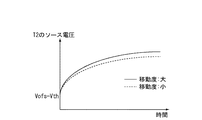
次に図11−2に示すように信号書込み期間/移動度補正期間(6)に入ると、信号線SLの電位をVofsからVsigに切り換えた後、サンプリング用トランジスタT1をオンする。このとき信号電位Vsigは階調に応じた電圧となっている。駆動用トランジスタT2のゲート電位はサンプリング用トランジスタT1をオンしているためVsigとなる。一方ソース電位は電源Vccから電流が流れるため時間と共に上昇していく。この時点でも駆動用トランジスタT2のソース電位が発光素子ELの閾電圧Vthelとカソード電圧Vcatの和を超えていなければ、駆動用トランジスタT2から流れる電流はもっぱら等価容量Celと保持容量C1の充電に使われる。このとき既に駆動用トランジスタT2の閾電圧補正動作は完了しているため、駆動用トランジスタT2が流す電流は移動度μを反映したものとなる。具体的に言うと移動度μが大きい駆動用トランジスタT2はこのときの電流量が大きく、ソースの電位上昇分ΔVも大きい。逆に移動度μが小さい場合駆動用トランジスタT2の電流量が小さく、ソースの上昇分ΔVは小さくなる。かかる動作により駆動用トランジスタT2のゲート電圧Vgsは移動度μを反映してΔVだけ圧縮され、移動度補正期間(6)が完了した時点で完全に移動度μを補正したVgsが得られる。 Next, as shown in FIG. 11B, when the signal writing period / mobility correction period (6) starts, the sampling transistor T1 is turned on after the potential of the signal line SL is switched from Vofs to Vsig. At this time, the signal potential Vsig is a voltage corresponding to the gradation. The gate potential of the driving transistor T2 is Vsig because the sampling transistor T1 is turned on. On the other hand, the source potential rises with time because current flows from the power supply Vcc. Even at this time, if the source potential of the driving transistor T2 does not exceed the sum of the threshold voltage Vthel and the cathode voltage Vcat of the light emitting element EL, the current flowing from the driving transistor T2 is exclusively used for charging the equivalent capacitor Cel and the holding capacitor C1. Is called. At this time, since the threshold voltage correction operation of the driving transistor T2 has already been completed, the current flowing through the driving transistor T2 reflects the mobility μ. Specifically, the driving transistor T2 having a high mobility μ has a large amount of current at this time, and the source potential increase ΔV is also large. On the contrary, when the mobility μ is small, the current amount of the driving transistor T2 is small, and the increase ΔV of the source is small. With this operation, the gate voltage Vgs of the driving transistor T2 is compressed by ΔV reflecting the mobility μ, and Vgs with the mobility μ completely corrected is obtained when the mobility correction period (6) is completed.
図11−3は、上述した移動度補正期間(6)における駆動用トランジスタT2のソース電圧の時間的な変化を示すグラフである。図示するように駆動用トランジスタT2の移動度が大きいとソース電圧は速く上昇し、それだけVgsが圧縮される。即ち移動度μが大きいとその影響を打ち消すようにVgsが圧縮され、駆動電流が抑制できる。一方移動度μが小さい場合駆動用トランジスタT2のソース電圧はそれほど速く上昇しないので、Vgsも強く圧縮を受けることはない。したがって移動度μが小さい場合、駆動用トランジスタのVgsは小さい駆動能力を補うように大きな圧縮がかからない。 FIG. 11C is a graph showing temporal changes in the source voltage of the driving transistor T2 during the mobility correction period (6) described above. As shown in the figure, when the mobility of the driving transistor T2 is large, the source voltage rises quickly, and Vgs is compressed accordingly. That is, when the mobility μ is large, Vgs is compressed so as to cancel the influence, and the drive current can be suppressed. On the other hand, when the mobility μ is small, the source voltage of the driving transistor T2 does not rise so fast, so that Vgs is not strongly compressed. Therefore, when the mobility μ is small, Vgs of the driving transistor is not compressed so as to compensate for the small driving capability.
図12は発光期間(7)の動作状態を表している。この発光期間(7)ではサンプリング用トランジスタT1をオフして発光素子ELを発光させる。駆動用トランジスタT2のゲートソース間電圧Vgsは一定に保たれており、駆動用トランジスタT2は前述した特性式に従って一定の電流Ids´を発光素子ELに流す。発光素子ELのアノード電圧(即ち駆動用トランジスタT2のソース電圧)は発光素子ELにIds´という電流が流れるため、Vxまで上昇しこれがVcat+Vthelを超えた時点で発光素子ELが発光する。発光素子ELは発光時間が長くなるとその電流/電圧特性は変化してしまう。そのため図11−3に示したソースSの電位が変化する。しかしながら駆動用トランジスタT2のゲートソース間電圧Vgsはブートストラップ動作により一定値に保たれているので、発光素子ELに流れる電流Ids´は変化しない。よって発光素子ELの電流/電圧特性が劣化しても、一定の駆動電流Ids´が常に流れていて、発光素子ELの輝度が変化することはない。 FIG. 12 shows an operation state in the light emission period (7). In this light emission period (7), the sampling transistor T1 is turned off to cause the light emitting element EL to emit light. The gate-source voltage Vgs of the driving transistor T2 is kept constant, and the driving transistor T2 supplies a constant current Ids ′ to the light emitting element EL according to the above-described characteristic equation. The anode voltage of the light emitting element EL (that is, the source voltage of the driving transistor T2) flows to the light emitting element EL, so that the current Ids ′ rises to Vx, and the light emitting element EL emits light when this exceeds Vcat + Vthel. The light emitting element EL changes its current / voltage characteristics as the light emission time becomes longer. For this reason, the potential of the source S shown in FIG. However, since the gate-source voltage Vgs of the driving transistor T2 is maintained at a constant value by the bootstrap operation, the current Ids ′ flowing through the light emitting element EL does not change. Therefore, even if the current / voltage characteristics of the light emitting element EL deteriorate, a constant drive current Ids ′ always flows, and the luminance of the light emitting element EL does not change.
ところで表示装置の高精細化及び高速化が進むと、1H期間が短くなるが、この場合でも、最後の1H以内に閾電圧補正動作及び信号電位書込動作を完了する必要がある。その際入力信号や制御信号のトランジェントを考慮した上で、信号線に対するVofsの入力、閾電圧補正動作、サンプリング用トランジスタT1のオフ動作、信号線SLに対する信号電位Vsigの入力、信号電位書込動作、サンプリング用トランジスタT1のオフ動作を1H以内に行わなければならない。しかしながら実際には表示装置の高精細化及び高速化が進むと、1Hが相当程度短縮化されるため、1H以内に閾電圧補正動作及び信号電位書込動作を完了することが困難である。 By the way, as the display device becomes higher in definition and speeded up, the 1H period becomes shorter. Even in this case, it is necessary to complete the threshold voltage correction operation and the signal potential writing operation within the last 1H. At that time, in consideration of the transient of the input signal and the control signal, the input of Vofs to the signal line, the threshold voltage correction operation, the off operation of the sampling transistor T1, the input of the signal potential Vsig to the signal line SL, and the signal potential writing operation The sampling transistor T1 must be turned off within 1H. However, in practice, when the display device is further refined and speeded up, 1H is considerably shortened, and it is difficult to complete the threshold voltage correction operation and the signal potential writing operation within 1H.
本発明は上述した問題点に対処するため、複数の水平期間を合成し、閾電圧補正動作をその合成した期間の一部で共通に行うものである。その後合成期間の残りの部分で順に信号電位書込動作を行う。図13はその一例として、2水平期間(2H)を合成した場合の動作シーケンスを模式的に示したタイミングチャートである。なお比較のため前述した参考例の動作シーケンスを本タイミングチャートの上段に示し、本発明の動作シーケンスを下段に示してある。参考例の動作シーケンスでは、入力信号は1H単位でVofsとVsigの間を切換る。Nライン目のサンプリング用トランジスタT1(N)には3個のパルスP0,P1,P2を含む制御信号が順次印加される。このパルスP0,P1,P2に応じてサンプリング用トランジスタT1(N)がオンする。位相が1H後方にシフトして同じくパルスP0,P1,P2を含む制御信号がN+1ライン目のサンプリング用トランジスタT1(N+1)に印加される。一番目の1H期間では入力信号がVofsのときサンプリング用トランジスタT1(N)が制御パルスP1に応じてオンし、閾電圧補正動作を行う。その後同じ1H期間で入力信号が信号電位Vsig1になると、サンプリング用トランジスタT1(N)が制御パルスP2に応じてオンし、信号電位書込動作を行う。この様にしてNライン目のサンプリング用トランジスタT1(N)は1番目の水平期間で閾電圧補正動作及び信号電位書込動作を完了する。なおこのとき次のラインのサンプリング用トランジスタT1(N+1)は制御パルスP0に応じてオンし、1回目の閾電圧補正動作を行っている。 In order to cope with the above-described problems, the present invention combines a plurality of horizontal periods and performs a threshold voltage correction operation in common for a part of the combined period. Thereafter, the signal potential writing operation is sequentially performed in the remaining part of the synthesis period. FIG. 13 is a timing chart schematically showing an operation sequence when two horizontal periods (2H) are combined as an example. For comparison, the operation sequence of the reference example described above is shown in the upper part of this timing chart, and the operation sequence of the present invention is shown in the lower part. In the operation sequence of the reference example, the input signal switches between Vofs and Vsig in units of 1H. A control signal including three pulses P0, P1, and P2 is sequentially applied to the sampling transistor T1 (N) on the Nth line. The sampling transistor T1 (N) is turned on in response to the pulses P0, P1, and P2. The control signal including the pulses P0, P1, P2 is applied to the sampling transistor T1 (N + 1) on the (N + 1) th line with the phase shifted 1H backward. In the first 1H period, when the input signal is Vofs, the sampling transistor T1 (N) is turned on according to the control pulse P1, and the threshold voltage correcting operation is performed. Thereafter, when the input signal becomes the signal potential Vsig1 in the same 1H period, the sampling transistor T1 (N) is turned on according to the control pulse P2, and the signal potential writing operation is performed. In this way, the sampling transistor T1 (N) on the Nth line completes the threshold voltage correcting operation and the signal potential writing operation in the first horizontal period. At this time, the sampling transistor T1 (N + 1) in the next line is turned on in response to the control pulse P0, and the first threshold voltage correction operation is performed.
2番目の水平期間に進むと、入力信号がVofsのとき、N+1ライン目のサンプリング用トランジスタT1(N+1)が制御パルスP1に応じてオンし、2回目の閾電圧補正動作を行う。続いて入力信号がVofsからVsig2に切換ると、サンプリング用トランジスタT1(N+1)は制御パルスP2に応じてオンし、信号電位書込動作を行う。この様にして、各ラインのサンプリング用トランジスタは、1H内で閾電圧補正動作と信号電位書込動作を行っている。本参考例では1回の閾電圧補正動作で補正が完了しないため、2回に分けて繰り返し閾電圧補正動作を行っている。 In the second horizontal period, when the input signal is Vofs, the sampling transistor T1 (N + 1) on the (N + 1) th line is turned on in response to the control pulse P1, and the second threshold voltage correcting operation is performed. Subsequently, when the input signal is switched from Vofs to Vsig2, the sampling transistor T1 (N + 1) is turned on in response to the control pulse P2, and the signal potential writing operation is performed. In this way, the sampling transistors in each line perform the threshold voltage correcting operation and the signal potential writing operation within 1H. In this reference example, the correction is not completed by a single threshold voltage correction operation, so the threshold voltage correction operation is repeatedly performed in two steps.
これに対し本発明にかかる動作シーケンスでは、ライトスキャナは複数の走査線(本実施例では2本)の各々に割り当てられている走査期間(1H)を合わせて第1期間及び第2期間を含む合成期間としている。換言すると、この合成走査期間は2Hに相当する。第1期間で2本の走査線(NラインとN+1ライン)に一斉に制御信号P1を出力して、一斉に閾電圧補正動作を実行する。続いて第2期間で2本の走査線(ラインNとラインN+1)に順次制御信号P2を出力して、順次信号電位書込動作を実行している。図示の例では入力信号は合成走査期間2Hの前半に相当する第1期間ではVofsであり、後半の第2期間では順にVsig1からVsig2に変化する。このときNライン目のサンプリング用トランジスタT1(N)は制御信号パルスP2に応じてオンし、Vsig1をサンプリングする。続いてN+1ライン目のサンプリング用トランジスタT1(N+1)が制御信号パルスP2に応じてオンし、Vsig2をサンプリングする。
On the other hand, in the operation sequence according to the present invention, the write scanner includes the first period and the second period in combination with the scanning period (1H) assigned to each of the plurality of scanning lines (two lines in this embodiment). The synthesis period. In other words, this combined scanning period corresponds to 2H. In the first period, the control signal P1 is output simultaneously to the two scanning lines (N line and N + 1 line), and the threshold voltage correction operation is executed simultaneously. Subsequently, the control signal P2 is sequentially output to the two scanning lines (line N and line N + 1) in the second period, and the signal potential writing operation is sequentially performed. In the illustrated example, the input signal is Vofs in the first period corresponding to the first half of the
図14は、電源ラインの電位変化を含めた本発明の動作シーケンスの全体構成を示すタイミングチャートである。図示するように、Nライン目とN+1ライン目において補正準備期間及び閾電圧補正期間でサンプリング用トランジスタT1(N),T1(N+1)に印加される制御信号波形は共通である。一方Nライン目の画素に対する信号書込み時間とN+1ライン目の画素に対する信号書込み時間の差は、1H以下となっている。さらに電源ラインDSがVssになる時間(非発光期間開始タイミング)もNライン目とN+1ライン目の差は1H未満となっている。非発光時に駆動用トランジスタのゲートをVofsとしソースをVssとした後、電源ラインをVssからVccに切換えて分割閾電圧補正動作を行う。その後移動度補正を行いながら信号電位Vsig1,Vsig2をそれぞれのラインの保持容量に書込み、発光素子ELを発光させている。以上のように本動作シーケンスでは、第2期間で1走査期間(1H)より小さい位相差で順次制御信号を各走査線WS(N,N+1)に出力している。電源スキャナは、第1期間で閾電圧補正動作を実行するため複数本の走査線WS(N,N+1)に対応した複数本の給電線DSに対して低電位Vssを供給した後一斉に高電位Vccに切り換えている。その際第1期間で1走査期間(1H)より小さい位相差で順次複数本の給電線DS(N,N+1)に低電位Vssを供給した後、一斉に高電位Vccに切換えている。 FIG. 14 is a timing chart showing the overall configuration of the operation sequence of the present invention including the change in potential of the power supply line. As shown in the figure, the control signal waveforms applied to the sampling transistors T1 (N) and T1 (N + 1) in the correction preparation period and the threshold voltage correction period in the Nth line and the N + 1th line are common. On the other hand, the difference between the signal writing time for the pixel on the N-th line and the signal writing time for the pixel on the N + 1-th line is 1H or less. Further, the difference between the Nth line and the (N + 1) th line is less than 1H in the time when the power line DS becomes Vss (non-light emission period start timing). At the time of non-light emission, the gate of the driving transistor is set to Vofs and the source is set to Vss, and then the power supply line is switched from Vss to Vcc to perform the division threshold voltage correction operation. Thereafter, the signal potentials Vsig1 and Vsig2 are written to the holding capacitors of the respective lines while performing mobility correction, and the light emitting element EL is caused to emit light. As described above, in this operation sequence, the control signals are sequentially output to the scanning lines WS (N, N + 1) with a phase difference smaller than one scanning period (1H) in the second period. The power supply scanner simultaneously supplies the low potential Vss to the plurality of power supply lines DS corresponding to the plurality of scanning lines WS (N, N + 1) in order to execute the threshold voltage correction operation in the first period, and then simultaneously increases the high potential. It is switched to Vcc. At this time, the low potential Vss is sequentially supplied to the plurality of power supply lines DS (N, N + 1) with a phase difference smaller than one scanning period (1H) in the first period, and then simultaneously switched to the high potential Vcc.
以上のように本発明では所定本数ごとに走査線を区分してブロック化し、且つ所定本数の走査線の各々に割り当てられた走査線を合成して、第1期間及び第2期間に分かれた1合成期間としている。図14に示したタイミングチャートでは理解を容易にするため2本ごとに走査線を区分してブロック化し、且つ2本の走査線の各々に割り当てられた1水平期間(1H)を合成して、第1期間及び第2期間に分かれた1合成期間(2H)としている。図14のタイミングチャートは、Nライン目の走査線とN+1ライン目の走査線からなる1ブロック分の動作シーケンスを表している。 As described above, according to the present invention, the scanning lines are divided into blocks every predetermined number, and the scanning lines assigned to each of the predetermined number of scanning lines are combined to be divided into the first period and the second period. The synthesis period. In the timing chart shown in FIG. 14, for easy understanding, the scanning lines are divided into blocks every two lines, and one horizontal period (1H) assigned to each of the two scanning lines is synthesized. One synthesis period (2H) divided into a first period and a second period is used. The timing chart of FIG. 14 represents an operation sequence for one block including the Nth scanning line and the (N + 1) th scanning line.
図15Aは、Nライン目の画素に含まれる駆動用トランジスタT2のゲート電位及びソース電位の変化を表した波形図である。ゲートG及びソースSの電位波形に対応して、電源ラインDSの変化、サンプリング用トランジスタT1の制御信号の変化及び信号線SLに供給される入力信号の電位変化も表してある。Nライン目の画素は電源ラインDSの電位変化やサンプリング用トランジスタT1の制御信号及び入力信号の変化に応じて、補正準備期間(4)、閾値補正期間(5)信号書込み期間(6)などで所定の動作を行う。 FIG. 15A is a waveform diagram showing changes in the gate potential and the source potential of the driving transistor T2 included in the pixel on the Nth line. Corresponding to the potential waveforms of the gate G and the source S, changes in the power supply line DS, changes in the control signal of the sampling transistor T1, and changes in the potential of the input signal supplied to the signal line SL are also shown. The pixel on the N-th line has a correction preparation period (4), a threshold correction period (5), a signal writing period (6), etc., according to the potential change of the power supply line DS and the control signal and input signal of the sampling transistor T1. Perform a predetermined operation.
準備期間(4)では駆動用トランジスタT2のゲートGがVofsに設定され、ソースSがVssに設定される。その後1回目の閾電圧補正期間(5)及び待機期間(5a)の後、2回目の閾電圧補正期間(5)でゲートGとソースSとの間の電圧VgsがVthに相当する電圧で固定される。 In the preparation period (4), the gate G of the driving transistor T2 is set to Vofs, and the source S is set to Vss. After that, after the first threshold voltage correction period (5) and standby period (5a), the voltage Vgs between the gate G and the source S is fixed at a voltage corresponding to Vth in the second threshold voltage correction period (5). Is done.
続いて移行期間(5b)の後信号書込み期間(6)に入って信号電位Vsig1の書込動作を行う。Nライン目の画素では、2回目の閾電圧補正期間(5)が終わって信号電位書込み期間(6)に入るまでの移行期間(5b)が非常に短い。移行期間(5b)では駆動用トランジスタT2の電流リークが若干あるため、ゲートG及びソースSの電位は変動する。しかしながらNライン目の画素では移行期間(5b)が非常に短いため、駆動用トランジスタT2の電流リークの影響はほとんど見られず、ソースSの電位変動はほとんどない。 Subsequently, after the transition period (5b), the signal writing period (6) is entered, and the signal potential Vsig1 is written. In the pixel on the Nth line, the transition period (5b) from the end of the second threshold voltage correction period (5) to the start of the signal potential writing period (6) is very short. In the transition period (5b), the potential of the gate G and the source S varies because there is a slight current leakage of the driving transistor T2. However, since the transition period (5b) is very short in the pixel on the N-th line, the influence of the current leakage of the driving transistor T2 is hardly observed, and the potential variation of the source S is hardly observed.
図15Bは、N+1ライン目の画素に属する駆動用トランジスタT2のゲートG及びソースSの電位変化を示す波形図である。前述した様にラインNとラインN+1は同一ブロックに属しており、閾電圧補正動作はブロック単位で一括して行われるが、信号電位書込動作はブロック内で順次行われる。そのため信号書込み期間(6)はNライン目の画素に比べN+1ライン目の画素が後方にシフトする。よって図15Bのタイミングチャートに示すように、2回目の閾電圧補正期間(5)から信号電位書込み期間(6)の間に介在する移行期間(5b)はNライン目の画素に比べN+1ライン目の画素が長くなっている。従って駆動用トランジスタT2の電流リークの影響を強く受け、点線の丸印で囲むように駆動用トランジスタT2のゲートG及びソースSの電位が上昇してしまう。特にソースSの電位上昇により、ゲート電位Gが上昇する。これによって保持容量C1に書き込まれる信号電位のダイナミックレンジが小さくなってしまい、N+1ライン目の画素は所望の輝度が取れず、Nライン目の画素に比べて輝度が下ってしまう。 FIG. 15B is a waveform diagram showing potential changes of the gate G and the source S of the driving transistor T2 belonging to the pixel on the (N + 1) th line. As described above, the line N and the line N + 1 belong to the same block, and the threshold voltage correction operation is collectively performed in units of blocks, but the signal potential writing operation is sequentially performed in the block. Therefore, in the signal writing period (6), the pixel on the (N + 1) th line shifts backward compared to the pixel on the Nth line. Therefore, as shown in the timing chart of FIG. 15B, the transition period (5b) interposed between the second threshold voltage correction period (5) and the signal potential writing period (6) is N + 1-th line compared to the N-th line pixel. The pixels are longer. Therefore, the potential of the gate G and the source S of the driving transistor T2 rises so as to be strongly affected by the current leakage of the driving transistor T2 and surrounded by the dotted circle. In particular, the gate potential G rises due to the potential rise of the source S. As a result, the dynamic range of the signal potential written to the storage capacitor C1 is reduced, and the pixel of the (N + 1) th line cannot obtain a desired luminance, and the luminance is lower than that of the pixel of the Nth line.
NラインとN+1ラインからなるブロックの動作が終わって次のブロックに進むと、N+2ラインとN+3ラインに対する動作がNライン及びN+1ラインの動作と同じ様に繰り返される。即ちN+2ラインの画素の移行期間は短く、N+3ラインの画素では閾電圧補正期間から信号書込み期間までの間の移行期間が長くなる。隣り合うブロック間で互いに隣接するN+1ラインでは移行期間が長く、N+2ラインでは移行期間が短い。従ってブロックの境界で移行期間が大きく異なることになり、輝度のむらがはっきりと現れてしまう。 When the operation of the block composed of the N line and the N + 1 line is finished and the operation proceeds to the next block, the operations for the N + 2 line and the N + 3 line are repeated in the same manner as the operations of the N line and the N + 1 line. That is, the transition period of the N + 2 line pixels is short, and the transition period between the threshold voltage correction period and the signal writing period is long in the N + 3 line pixels. N + 1 lines adjacent to each other between adjacent blocks have a long transition period, and N + 2 lines have a short transition period. Therefore, the transition period is greatly different at the block boundaries, and uneven brightness appears clearly.
本発明では上述した問題点に対処するため、隣り合うブロックで、各走査線に順次制御信号を出力して線順次走査を行う方向を互いに逆にしている。これにより隣り合うブロック間で互いに隣り合うラインに属する画素は、閾電圧補正動作を完了してから信号電位書込動作に入るまでの移行時間が同一になる。これにより隣り合うブロックの境界で互いに隣り合う一対のライン間に輝度の違いが現れず、むらの目立たない表示が得られる。 In the present invention, in order to cope with the above-described problems, the control signals are sequentially output to the respective scanning lines in the adjacent blocks to reverse the directions in which the line sequential scanning is performed. As a result, the pixels belonging to the adjacent lines between the adjacent blocks have the same transition time from the completion of the threshold voltage correction operation to the start of the signal potential write operation. As a result, a difference in luminance does not appear between a pair of adjacent lines at the boundary between adjacent blocks, and a non-conspicuous display is obtained.
図15Cは本発明の動作シーケンスを示すタイミングチャートである。本実施形態は一例として2本の走査線を1ブロックとし2水平期間(2H)を1合成期間とした場合である。図15Cの例では、NラインとN+1ラインを1ブロックとし、N+2ラインとN+3ラインを次のブロックにしている。従って互いに隣り合うブロックの境界はN+1ラインとN+2ラインの間になる。タイミングチャートに示すように、互いに隣り合うブロック間で、信号書き込み順及び電源ラインの電位切換え順、さらには信号入力順を反転させている。 FIG. 15C is a timing chart showing the operation sequence of the present invention. In the present embodiment, as an example, two scanning lines are set as one block, and two horizontal periods (2H) are set as one synthesis period. In the example of FIG. 15C, the N line and the N + 1 line are set as one block, and the N + 2 line and the N + 3 line are set as the next block. Therefore, the boundary between adjacent blocks is between the N + 1 line and the N + 2 line. As shown in the timing chart, the signal writing order, the power supply line potential switching order, and the signal input order are reversed between adjacent blocks.
この様に隣り合うブロックで信号書き込み時行う線順次走査の方向を反転することで、閾値補正動作を終了してから信号書込動作に入るまでの移行時間が、N+1ラインとN+2ラインで同じになっている。なおN+1ラインとN+2ラインは別々のブロックに属するため、電源ライン(N)と電源ライン(N+2)の切換えタイミングは位相差が2Hである。またサンプリング用トランジスタT1(N+1)とT1(N+2)に印加する制御信号パルスの位相差も1合成期間である2Hとなっている。これに合わせて入力信号はVsig(N)、Vsig(N+1)、Vsig(N+3)、Vsig(N+2)の順で変化している。つまりブロック間の線順次走査の反転に合わせて、Vsig(N+3)とVsig(N+2)が入れ替わっている。 By reversing the direction of line sequential scanning performed at the time of signal writing in adjacent blocks in this way, the transition time from the end of the threshold correction operation to the start of the signal writing operation is the same for the N + 1 line and the N + 2 line. It has become. Since the N + 1 line and the N + 2 line belong to different blocks, the switching timing of the power supply line (N) and the power supply line (N + 2) has a phase difference of 2H. The phase difference between the control signal pulses applied to the sampling transistors T1 (N + 1) and T1 (N + 2) is also 2H, which is one synthesis period. In accordance with this, the input signal changes in the order of Vsig (N), Vsig (N + 1), Vsig (N + 3), and Vsig (N + 2). That is, Vsig (N + 3) and Vsig (N + 2) are switched in accordance with the inversion of the line sequential scanning between the blocks.
閾電圧補正動作を終了してから信号電位書込動作に入るまでの移行時間を図15Cのタイミングチャートのように設定することで、別々のブロックに属するN+1ライン目の画素とN+2ライン目の画素の間で駆動用トランジスタの電流リーク量をほぼ同じとすることができ、参考例では視認されていたN+1ライン目の画素とN+2ライン目の画素との間の輝度差が目立たなくなる。これにより周期的なむらのない均一な画質を得ることができる。このような書込動作を実現するため、信号出力は隣接する合成期間で逆にする必要がある。 By setting the transition time from the end of the threshold voltage correction operation to the start of the signal potential writing operation as shown in the timing chart of FIG. 15C, the pixels on the N + 1 line and the pixels on the N + 2 line belonging to different blocks The current leakage amount of the driving transistors can be made substantially the same between the pixels of the N + 1 line and the pixels of the N + 2 line, which were visually recognized in the reference example, and the luminance difference becomes inconspicuous. Thereby, uniform image quality without periodic unevenness can be obtained. In order to realize such a writing operation, the signal output needs to be reversed in the adjacent synthesis period.
図15Dは画素アレイ部1に表示される画面の状態を示した模式的な平面図である。この参考例は画素アレイ部1に400本の走査線(400ライン)が形成され、これが100本ずつに束ねられて4個のブロックB1,B2,B3,B4に分割した例である。前述した様に閾電圧補正動作はブロック順次で各ブロックごと一括して行われる。一方信号電位書込動作は各ブロック内で線順次に行われる。本参考例は各ブロックB1〜B4で、それぞれ線順次走査の方向を上から下にした場合である。換言すると隣り合うブロック間で線順次走査の方向を反転させていない場合である。
FIG. 15D is a schematic plan view showing the state of the screen displayed on the
最初にブロックB1で閾電圧補正動作を一括して行い、続いて信号書き込みのための線順次走査を上から下に向かって行う。下に進むほど閾電圧補正動作が終わってから信号書込動作に入るまでの移行時間が長くなるため、その分電流リーク量が大きくなり輝度が低下する。図示の画面はブロックB1内で上から下に向かってわずかではあるが輝度が低下していく。これは移行時間が長くなるにつれ電流リークが増え、輝度が低下するためである。以下本明細書では説明の都合上移行時間をリーク時間と定義し直すことにする。 First, the threshold voltage correction operation is collectively performed in the block B1, and then line sequential scanning for signal writing is performed from the top to the bottom. As it goes down, the transition time from the end of the threshold voltage correction operation to the start of the signal writing operation becomes longer, so that the amount of current leakage increases and the luminance decreases accordingly. In the screen shown in the figure, the luminance decreases slightly from top to bottom in the block B1. This is because current leakage increases and the luminance decreases as the transition time increases. Hereinafter, in the present specification, the transition time is redefined as the leak time for convenience of explanation.
次のブロックB2で再び一括して閾電圧補正動作を行った後、信号書込動作を線順次走査で行う。線順次走査の方向はブロックB1と同じくブロックB2でも画面の上から下に向かっている。よってブロックB2内で輝度は上から下に向かって徐々に輝度が低下している。 In the next block B2, the threshold voltage correction operation is again performed collectively, and then the signal writing operation is performed by line sequential scanning. The direction of line sequential scanning is from the top to the bottom of the screen in block B2 as well as in block B1. Therefore, the luminance gradually decreases from top to bottom in the block B2.
ここでブロックB1とブロックB2の境界に着目すると、ブロックB1の最後のラインのリーク時間は最も長くなっている。これと隣り合うブロックB2の最初のラインはリーク時間が最も短い。従ってブロックB1とブロックB2の境界で互いに隣り合うラインのリーク時間が最も大きく相違しており、この境界に沿って一番大きな輝度の差が生じる。従って画素アレイ部1の画面を全体的に見た場合、図示のようにブロックB1,B2,B3,B4単位で帯状のむらが視認されることになり、画面のユニフォーミティが悪くなる。
Here, focusing on the boundary between the block B1 and the block B2, the leak time of the last line of the block B1 is the longest. The first line of the block B2 adjacent to this has the shortest leak time. Therefore, the leak times of the lines adjacent to each other at the boundary between the block B1 and the block B2 are the largest, and the greatest difference in luminance occurs along this boundary. Therefore, when the screen of the
図15Eは本発明の動作シーケンスに従って画素アレイ部1上に表示される画面の状態を示した模式的な平面図である。図15Dと同様に、画素アレイ部1に含まれる400本の走査線(400ライン)は4つのブロックB1,B2,B3,B4に100本ずつ別れている。ブロックB1の線順次走査とブロックB2の線順次走査は方向が反転している。同様にブロックB2とB3でも線順次走査の方向は反転している。さらにB3とB4の間でも線順次走査の方向は互いに反転している。最初のブロックB1に着目すると、信号書き込みのための線順次走査は上から下に向かって進む。従ってブロックB1の最終ラインのリーク時間が最も長い。続いてブロックB2になると逆に線順次走査は下から上に向かって行われる。よってブロックB2の先頭に位置するラインが最もリーク時間が長くなる。ブロックB1とブロックB2の境界に着目すると互いに隣り合うラインは最もリーク時間が長くなっており、両者の輝度差はない。換言するとブロックB1とブロックB2の境界で輝度差は現れない。
FIG. 15E is a schematic plan view showing the state of the screen displayed on the
続いてブロックB2のB3の境界に着目すると、ブロックB2側の最終ラインのリーク時間は最も短い。ブロックB3は線順次走査をブロックB2とは逆に上から下に向かって行うため、B3の最初のラインのリーク時間が最も短い。よってブロックB2とブロックB3の境界で互いに隣り合うラインはリーク時間が共に最も短く、輝度差はない。従ってブロックB2とブロックB3の間で顕著な輝度むらはなく、均一な輝度分布が得られる。 Subsequently, when focusing on the boundary of B3 of block B2, the leak time of the last line on the block B2 side is the shortest. Since the block B3 performs line sequential scanning from the top to the bottom as opposed to the block B2, the leak time of the first line of B3 is the shortest. Therefore, the lines adjacent to each other at the boundary between the block B2 and the block B3 have the shortest leak time and no luminance difference. Therefore, there is no noticeable luminance unevenness between the block B2 and the block B3, and a uniform luminance distribution is obtained.
本発明にかかる表示装置は、図16に示すような薄膜デバイス構成を有する。本図は、絶縁性の基板に形成された画素の模式的な断面構造を表している。図示するように、画素は、複数の薄膜トランジタを含むトランジスター部(図では1個のTFTを例示)、保持容量などの容量部及び有機EL素子などの発光部とを含む。基板の上にTFTプロセスでトランジスター部や容量部が形成され、その上に有機EL素子などの発光部が積層されている。その上に接着剤を介して透明な対向基板を貼り付けてフラットパネルとしている。 The display device according to the present invention has a thin film device configuration as shown in FIG. This figure shows a schematic cross-sectional structure of a pixel formed on an insulating substrate. As shown in the figure, the pixel includes a transistor part (a single TFT is illustrated in the figure) including a plurality of thin film transistors, a capacitor part such as a storage capacitor, and a light emitting part such as an organic EL element. A transistor portion and a capacitor portion are formed on a substrate by a TFT process, and a light emitting portion such as an organic EL element is laminated thereon. A transparent counter substrate is pasted thereon via an adhesive to form a flat panel.
本発明にかかる表示装置は、図17に示すようにフラット型のモジュール形状のものを含む。例えば絶縁性の基板上に、有機EL素子、薄膜トランジスタ、薄膜容量等からなる画素をマトリックス状に集積形成した画素アレイ部を設ける、この画素アレイ部(画素マトリックス部)を囲むように接着剤を配し、ガラス等の対向基板を貼り付けて表示モジュールとする。この透明な対向基板には必要に応じて、カラーフィルタ、保護膜、遮光膜等を設けてももよい。表示モジュールには、外部から画素アレイ部への信号等を入出力するためのコネクタとして例えばFPC(フレキシブルプリントサーキット)を設けてもよい。 The display device according to the present invention includes a flat module-shaped display as shown in FIG. For example, a pixel array unit in which pixels made up of organic EL elements, thin film transistors, thin film capacitors and the like are integrated in a matrix is provided on an insulating substrate, and an adhesive is disposed so as to surround the pixel array unit (pixel matrix unit). Then, a counter substrate such as glass is attached to form a display module. If necessary, this transparent counter substrate may be provided with a color filter, a protective film, a light shielding film, and the like. For example, an FPC (flexible printed circuit) may be provided in the display module as a connector for inputting / outputting a signal to / from the pixel array unit from the outside.
以上説明した本発明における表示装置は、フラットパネル形状を有し、様々な電子機器、例えば、デジタルカメラ、ノート型パーソナルコンピューター、携帯電話、ビデオカメラなど、電子機器に入力された、若しくは、電子機器内で生成した映像信号を画像若しくは映像として表示するあらゆる分野の電子機器のディスプレイに適用することが可能である。以下この様な表示装置が適用された電子機器の例を示す。 The display device according to the present invention described above has a flat panel shape and is input to an electronic device such as a digital camera, a notebook personal computer, a mobile phone, or a video camera, or an electronic device. It is possible to apply to the display of the electronic device of all fields which display the image signal produced | generated in the inside as an image or an image | video. Examples of electronic devices to which such a display device is applied are shown below.
図18は本発明が適用されたテレビであり、フロントパネル12、フィルターガラス13等から構成される映像表示画面11を含み、本発明の表示装置をその映像表示画面11に用いることにより作製される。
FIG. 18 shows a television to which the present invention is applied, which includes a
図19は本発明が適用されたデジタルカメラであり、上が正面図で下が背面図である。このデジタルカメラは、撮像レンズ、フラッシュ用の発光部15、表示部16、コントロールスイッチ、メニュースイッチ、シャッター19等を含み、本発明の表示装置をその表示部16に用いることにより作製される。
FIG. 19 shows a digital camera to which the present invention is applied, in which the top is a front view and the bottom is a back view. This digital camera includes an imaging lens, a
図20は本発明が適用されたノート型パーソナルコンピュータであり、本体20には文字等を入力するとき操作されるキーボード21を含み、本体カバーには画像を表示する表示部22を含み、本発明の表示装置をその表示部22に用いることにより作製される。
FIG. 20 shows a notebook personal computer to which the present invention is applied. The
図21は本発明が適用された携帯端末装置であり、左が開いた状態を表し、右が閉じた状態を表している。この携帯端末装置は、上側筐体23、下側筐体24、連結部(ここではヒンジ部)25、ディスプレイ26、サブディスプレイ27、ピクチャーライト28、カメラ29等を含み、本発明の表示装置をそのディスプレイ26やサブディスプレイ27に用いることにより作製される。
FIG. 21 shows a mobile terminal device to which the present invention is applied. The left side shows an open state and the right side shows a closed state. The portable terminal device includes an
図22は本発明が適用されたビデオカメラであり、本体部30、前方を向いた側面に被写体撮影用のレンズ34、撮影時のスタート/ストップスイッチ35、モニター36等を含み、本発明の表示装置をそのモニター36に用いることにより作製される。
FIG. 22 shows a video camera to which the present invention is applied. The video camera includes a
1・・・画素アレイ、2・・・画素、3・・・水平セレクタ(信号ドライバ)、4・・・制御用スキャナ、5・・・電源スキャナ、T1・・・サンプリング用トランジスタ、T2・・・駆動用トランジスタ、C1・・・保持容量、EL・・・発光素子、WS・・・走査線、DS・・・給電線、SL・・・信号線
DESCRIPTION OF
Claims (5)
所定の本数ごとに区分された走査線群に対応する画素のブロック単位で行列状の画素を順次駆動するブロック順次駆動を行うと共に、隣り合うブロック間にあっては線順次駆動の走査方向が互いに逆になるように、各ブロックにおいて各走査線を走査して画素を行単位で順次駆動する線順次駆動を行う駆動部、
を備えており、
駆動部は、
階調に応じた信号電位と所定の基準電位とに切り換わる映像信号を信号線に供給する信号セレクタ、
隣り合うブロック間にあっては線順次駆動の走査方向が互いに逆になるように、走査線に制御信号を供給して画素を線順次駆動するライトスキャナ、及び、
ブロック毎に纏められた給電線に高電位と低電位とに切り換わる電源電圧を供給するドライブスキャナ、
を有しており、
画素は、
一方の電流端が信号線に接続され、制御端が走査線に接続されたサンプリング用トランジスタ、
給電線にドレインが接続され、サンプリング用トランジスタの他方の電流端にゲートが接続された駆動用トランジスタ、
駆動用トランジスタのソースに接続された発光素子、及び、
駆動用トランジスタのソースとゲートとの間に接続された保持容量、
を有しており、
駆動部によって、
信号線に基準電位が供給されているときにサンプリング用トランジスタを導通状態とするようにブロック内の画素を順次走査することによって点灯状態の発光素子を消灯状態に切り換える消灯動作が行われ、次いで、
ブロックに対応する給電線の電源電圧が高電位から低電位に切り換えらることによって画素の駆動トランジスタのソースの電圧を下げ、その後、給電線の電源電圧が高電位に戻される補正準備動作が行われ、次いで、
信号線が基準電位のときにサンプリング用トランジスタを導通状態とするようにブロック内の画素が順次走査され、駆動用トランジスタのゲートとソース間の電圧が駆動用トランジスタの閾電圧に向うように保持容量を放電する補正動作が行われる、
表示装置。 A plurality of scan lines disposed in rows, a plurality of signal lines arranged in columns, and a pixel array section in which each scanning line and each signal line is provided with a matrix of picture element disposed at the intersection And
Block sequential driving is performed to sequentially drive matrix pixels in units of pixel blocks corresponding to scanning line groups divided by a predetermined number, and the scanning direction of line sequential driving is reversed between adjacent blocks. A drive unit that performs line-sequential driving for scanning each scanning line in each block and sequentially driving pixels in units of rows ,
With
The drive unit
A signal selector that supplies a video signal to a signal line that switches between a signal potential corresponding to a gradation and a predetermined reference potential;
A write scanner that supplies a control signal to the scanning lines to drive the pixels line-sequentially so that the scanning directions of the line-sequential driving are opposite to each other between adjacent blocks; and
A drive scanner that supplies a power supply voltage that switches between a high potential and a low potential to a power supply line assembled for each block;
Have
Pixel is
A sampling transistor having one current end connected to a signal line and a control end connected to a scanning line;
A driving transistor having a drain connected to the power supply line and a gate connected to the other current end of the sampling transistor;
A light emitting device connected to the source of the driving transistor, and
A storage capacitor connected between the source and gate of the driving transistor,
Have
Depending on the drive unit,
When the reference potential is supplied to the signal line, a turn-off operation is performed in which the light-emitting elements that are turned on are turned off by sequentially scanning the pixels in the block so that the sampling transistor is turned on.
The power supply voltage of the power supply line corresponding to the block is switched from a high potential to a low potential to lower the voltage of the source of the pixel drive transistor, and then a correction preparation operation is performed in which the power supply voltage of the power supply line is returned to the high potential Then
When the signal line is at the reference potential, the pixels in the block are sequentially scanned so that the sampling transistor is turned on, and the storage capacitor is set so that the voltage between the gate and source of the driving transistor is directed to the threshold voltage of the driving transistor. Corrective action is taken to discharge the
Display device.
補正動作の後、駆動部によって、信号線が信号電位のときにサンプリング用トランジスタを導通状態とするようにブロック内の画素が順次走査され、信号電位を保持容量に書き込む書込動作が行われる請求項1に記載の表示装置。After the correction operation, the drive unit sequentially scans the pixels in the block so that the sampling transistor is turned on when the signal line is at the signal potential, and performs a writing operation to write the signal potential to the storage capacitor. Item 4. The display device according to Item 1.
所定の本数ごとに区分された走査線群に対応する画素のブロック単位で行列状の画素を順次駆動するブロック順次駆動を行うと共に、隣り合うブロック間にあっては線順次駆動の走査方向が互いに逆になるように、各ブロックにおいて各走査線を走査して画素を行単位で順次駆動する線順次駆動を行う駆動部、
を備えており、
駆動部は、
階調に応じた信号電位と所定の基準電位とに切り換わる映像信号を信号線に供給する信号セレクタ、
隣り合うブロック間にあっては線順次駆動の走査方向が互いに逆になるように、走査線に制御信号を供給して画素を線順次駆動するライトスキャナ、及び、
ブロック毎に纏められた給電線に高電位と低電位とに切り換わる電源電圧を供給するドライブスキャナ、
を有しており、
画素は、
一方の電流端が信号線に接続され、制御端が走査線に接続されたサンプリング用トランジスタ、
給電線にドレインが接続され、サンプリング用トランジスタの他方の電流端にゲートが接続された駆動用トランジスタ、
駆動用トランジスタのソースに接続された発光素子、及び、
駆動用トランジスタのソースとゲートとの間に接続された保持容量、
を有している表示装置の駆動方法であって、
駆動部は、
信号線に基準電位が供給されているときにサンプリング用トランジスタを導通状態とするようにブロック内の画素を順次走査することによって点灯状態の発光素子を消灯状態に切り換える消灯動作を行い、次いで、
ブロックに対応する給電線の電源電圧を高電位から低電位に切り換えることによって画素の駆動トランジスタのソースの電圧を下げ、その後、給電線の電源電圧を高電位に戻す補正準備動作を行い、次いで、
信号線が基準電位のときにサンプリング用トランジスタを導通状態とするようにブロック内の画素を順次走査し、駆動用トランジスタのゲートとソース間の電圧が駆動用トランジスタの閾電圧に向うように保持容量を放電する補正動作を行う、
表示装置の駆動方法。 A plurality of scan lines disposed in rows, a plurality of signal lines arranged in columns, and a pixel array section in which each scanning line and each signal line is provided with a matrix of picture element disposed at the intersection And
Block sequential driving is performed to sequentially drive matrix pixels in units of pixel blocks corresponding to scanning line groups divided by a predetermined number, and the scanning direction of line sequential driving is reversed between adjacent blocks. A drive unit that performs line-sequential driving for scanning each scanning line in each block and sequentially driving pixels in units of rows ,
With
The drive unit
A signal selector that supplies a video signal to a signal line that switches between a signal potential corresponding to a gradation and a predetermined reference potential;
A write scanner that supplies a control signal to the scanning lines to drive the pixels line-sequentially so that the scanning directions of the line-sequential driving are opposite to each other between adjacent blocks; and
A drive scanner that supplies a power supply voltage that switches between a high potential and a low potential to a power supply line assembled for each block;
Have
Pixel is
A sampling transistor having one current end connected to a signal line and a control end connected to a scanning line;
A driving transistor having a drain connected to the power supply line and a gate connected to the other current end of the sampling transistor;
A light emitting device connected to the source of the driving transistor, and
A storage capacitor connected between the source and gate of the driving transistor,
A driving method of a display device having
The drive unit
Performing a light-off operation to switch a light-emitting element in a light-on state to a light-off state by sequentially scanning the pixels in the block so that the sampling transistor is turned on when a reference potential is supplied to the signal line,
By switching the power supply voltage of the power supply line corresponding to the block from a high potential to a low potential, the voltage of the source of the drive transistor of the pixel is lowered, and then a correction preparation operation is performed to return the power supply voltage of the power supply line to a high potential,
The pixels in the block are sequentially scanned so that the sampling transistor is turned on when the signal line is at the reference potential, and the storage capacitor is set so that the voltage between the gate and source of the driving transistor is directed to the threshold voltage of the driving transistor. Corrective action to discharge
A driving method of a display device.
表示部は、
行状に配された複数の走査線、列状に配された複数の信号線、及び、各走査線と各信号線とが交差する部分に配された行列状の画素を備えた画素アレイ部、並びに、
所定の本数ごとに区分された走査線群に対応する画素のブロック単位で行列状の画素を順次駆動するブロック順次駆動を行うと共に、隣り合うブロック間にあっては線順次駆動の走査方向が互いに逆になるように、各ブロックにおいて各走査線を走査して画素を行単位で順次駆動する線順次駆動を行う駆動部、
を備えており、
駆動部は、
階調に応じた信号電位と所定の基準電位とに切り換わる映像信号を信号線に供給する信号セレクタ、
隣り合うブロック間にあっては線順次駆動の走査方向が互いに逆になるように、走査線に制御信号を供給して画素を線順次駆動するライトスキャナ、及び、
ブロック毎に纏められた給電線に高電位と低電位とに切り換わる電源電圧を供給するドライブスキャナ、
を有しており、
画素は、
一方の電流端が信号線に接続され、制御端が走査線に接続されたサンプリング用トランジスタ、
給電線にドレインが接続され、サンプリング用トランジスタの他方の電流端にゲートが接続された駆動用トランジスタ、
駆動用トランジスタのソースに接続された発光素子、及び、
駆動用トランジスタのソースとゲートとの間に接続された保持容量、
を有しており、
駆動部によって、
信号線に基準電位が供給されているときにサンプリング用トランジスタを導通状態とするようにブロック内の画素を順次走査することによって点灯状態の発光素子を消灯状態に切り換える消灯動作が行われ、次いで、
ブロックに対応する給電線の電源電圧が高電位から低電位に切り換えらることによって画素の駆動トランジスタのソースの電圧を下げ、その後、給電線の電源電圧が高電位に戻される補正準備動作が行われ、次いで、
信号線が基準電位のときにサンプリング用トランジスタを導通状態とするようにブロック内の画素が順次走査され、駆動用トランジスタのゲートとソース間の電圧が駆動用トランジスタの閾電圧に向うように保持容量を放電する補正動作が行われる、
電子機器。 Consists of a Main body portion, a display unit for displaying the information outputted from the information or the main body is input to the main body portion,
The display section
A plurality of scan lines disposed in rows, a plurality of signal lines arranged in columns, and a pixel array section in which each scanning line and each signal line is provided with a matrix of picture element disposed at the intersection And
Block sequential driving is performed to sequentially drive matrix pixels in units of pixel blocks corresponding to scanning line groups divided by a predetermined number, and the scanning direction of line sequential driving is reversed between adjacent blocks. A drive unit that performs line-sequential driving for scanning each scanning line in each block and sequentially driving pixels in units of rows ,
With
The drive unit
A signal selector that supplies a video signal to a signal line that switches between a signal potential corresponding to a gradation and a predetermined reference potential;
A write scanner that supplies a control signal to the scanning lines to drive the pixels line-sequentially so that the scanning directions of the line-sequential driving are opposite to each other between adjacent blocks; and
A drive scanner that supplies a power supply voltage that switches between a high potential and a low potential to a power supply line assembled for each block;
Have
Pixel is
A sampling transistor having one current end connected to a signal line and a control end connected to a scanning line;
A driving transistor having a drain connected to the power supply line and a gate connected to the other current end of the sampling transistor;
A light emitting device connected to the source of the driving transistor, and
A storage capacitor connected between the source and gate of the driving transistor,
Have
Depending on the drive unit,
When the reference potential is supplied to the signal line, a turn-off operation is performed in which the light-emitting elements that are turned on are turned off by sequentially scanning the pixels in the block so that the sampling transistor is turned on.
The power supply voltage of the power supply line corresponding to the block is switched from a high potential to a low potential to lower the voltage of the source of the pixel drive transistor, and then a correction preparation operation is performed in which the power supply voltage of the power supply line is returned to the high potential. Then
When the signal line is at the reference potential, the pixels in the block are sequentially scanned so that the sampling transistor is turned on, and the storage capacitor is set so that the voltage between the gate and source of the driving transistor is directed to the threshold voltage of the driving transistor. Corrective action is taken to discharge the
Electronics.
Priority Applications (5)
| Application Number | Priority Date | Filing Date | Title |
|---|---|---|---|
| JP2008259166A JP5287111B2 (en) | 2007-11-14 | 2008-10-06 | Display device, driving method thereof, and electronic apparatus |
| TW97141028A TWI408644B (en) | 2007-11-14 | 2008-10-24 | A display device and a driving method thereof, and an electronic device |
| KR1020080111475A KR101517110B1 (en) | 2007-11-14 | 2008-11-11 | Display apparatus driving method for display apparatus and electronic apparatus |
| US12/292,181 US8937583B2 (en) | 2007-11-14 | 2008-11-13 | Display apparatus, driving method for display apparatus and electronic apparatus |
| CN2008101734702A CN101436382B (en) | 2007-11-14 | 2008-11-14 | Display apparatus, driving method for display apparatus and electronic apparatus |
Applications Claiming Priority (3)
| Application Number | Priority Date | Filing Date | Title |
|---|---|---|---|
| JP2007295555 | 2007-11-14 | ||
| JP2007295555 | 2007-11-14 | ||
| JP2008259166A JP5287111B2 (en) | 2007-11-14 | 2008-10-06 | Display device, driving method thereof, and electronic apparatus |
Related Child Applications (1)
| Application Number | Title | Priority Date | Filing Date |
|---|---|---|---|
| JP2012271884A Division JP2013068968A (en) | 2007-11-14 | 2012-12-13 | Display device, driving method thereof, and electronic apparatus |
Publications (3)
| Publication Number | Publication Date |
|---|---|
| JP2009139928A JP2009139928A (en) | 2009-06-25 |
| JP2009139928A5 JP2009139928A5 (en) | 2011-10-13 |
| JP5287111B2 true JP5287111B2 (en) | 2013-09-11 |
Family
ID=40710798
Family Applications (2)
| Application Number | Title | Priority Date | Filing Date |
|---|---|---|---|
| JP2008259166A Active JP5287111B2 (en) | 2007-11-14 | 2008-10-06 | Display device, driving method thereof, and electronic apparatus |
| JP2012271884A Pending JP2013068968A (en) | 2007-11-14 | 2012-12-13 | Display device, driving method thereof, and electronic apparatus |
Family Applications After (1)
| Application Number | Title | Priority Date | Filing Date |
|---|---|---|---|
| JP2012271884A Pending JP2013068968A (en) | 2007-11-14 | 2012-12-13 | Display device, driving method thereof, and electronic apparatus |
Country Status (3)
| Country | Link |
|---|---|
| JP (2) | JP5287111B2 (en) |
| CN (1) | CN101436382B (en) |
| TW (1) | TWI408644B (en) |
Families Citing this family (22)
| Publication number | Priority date | Publication date | Assignee | Title |
|---|---|---|---|---|
| JP4640449B2 (en) | 2008-06-02 | 2011-03-02 | ソニー株式会社 | Display device, driving method thereof, and electronic apparatus |
| JP2010002498A (en) | 2008-06-18 | 2010-01-07 | Sony Corp | Panel and drive control method |
| JP4784780B2 (en) * | 2008-06-30 | 2011-10-05 | ソニー株式会社 | Display device, driving method thereof, and electronic apparatus |
| JP2010020034A (en) * | 2008-07-10 | 2010-01-28 | Sony Corp | Image display device |
| EP2405418B1 (en) * | 2009-03-06 | 2015-08-12 | Joled Inc. | Image display apparatus and driving method therefor |
| JP5230806B2 (en) * | 2009-05-26 | 2013-07-10 | パナソニック株式会社 | Image display device and driving method thereof |
| JP5321304B2 (en) * | 2009-07-14 | 2013-10-23 | ソニー株式会社 | Display device, driving method thereof, and electronic apparatus |
| JP5477004B2 (en) * | 2010-01-14 | 2014-04-23 | ソニー株式会社 | Display device and display driving method |
| JP2011145531A (en) * | 2010-01-15 | 2011-07-28 | Sony Corp | Display device, method for driving the same, and electronic equipment |
| JP5532964B2 (en) | 2010-01-28 | 2014-06-25 | ソニー株式会社 | Display device and display driving method |
| MY155668A (en) * | 2010-04-02 | 2015-11-13 | Sharp Kk | Display device and drive method therefor |
| KR101291444B1 (en) | 2010-09-06 | 2013-07-30 | 파나소닉 주식회사 | Display device and method for driving the same |
| CN102714019B (en) | 2010-09-06 | 2015-07-08 | 株式会社日本有机雷特显示器 | Display device and drive method therefor |
| CN102549646B (en) | 2010-09-06 | 2014-07-16 | 松下电器产业株式会社 | Display device and method of driving same |
| WO2012032559A1 (en) * | 2010-09-06 | 2012-03-15 | パナソニック株式会社 | Display device and drive method therefor |
| JP2013092674A (en) * | 2011-10-26 | 2013-05-16 | Sony Corp | Drive circuit, drive method, display device, and electronic device |
| US9443471B2 (en) | 2012-07-31 | 2016-09-13 | Sharp Kabushiki Kaisha | Display device and driving method thereof |
| JP5962533B2 (en) * | 2013-02-13 | 2016-08-03 | ソニー株式会社 | Solid-state imaging device, driving method, and imaging apparatus |
| CN105609074B (en) * | 2016-01-25 | 2018-11-06 | 京东方科技集团股份有限公司 | A kind of shift-register circuit, array substrate and display device |
| CN108364982B (en) * | 2018-02-01 | 2020-12-22 | 武汉华星光电半导体显示技术有限公司 | OLED display device |
| US10339869B1 (en) | 2018-02-01 | 2019-07-02 | Wuhan China Star Optoelectronics Semiconductor Display Technology Co., Ltd. | OLED display device |
| CN110752240B (en) * | 2019-10-31 | 2022-03-01 | Oppo广东移动通信有限公司 | Display device and electronic apparatus |
Family Cites Families (22)
| Publication number | Priority date | Publication date | Assignee | Title |
|---|---|---|---|---|
| JP2002196721A (en) * | 2000-12-25 | 2002-07-12 | Sony Corp | Electroluminescence display and driving method for the same |
| JP2003122303A (en) * | 2001-10-16 | 2003-04-25 | Matsushita Electric Ind Co Ltd | El display panel and display device using the same, and its driving method |
| JP2004145300A (en) * | 2002-10-03 | 2004-05-20 | Seiko Epson Corp | Electronic circuit, method for driving electronic circuit, electronic device, electrooptical device, method for driving electrooptical device, and electronic apparatus |
| KR100487439B1 (en) * | 2002-12-31 | 2005-05-03 | 엘지.필립스 엘시디 주식회사 | Circuit and method for bi-directional driving plat display device |
| JP4734529B2 (en) * | 2003-02-24 | 2011-07-27 | 奇美電子股▲ふん▼有限公司 | Display device |
| JP2004046235A (en) * | 2003-09-05 | 2004-02-12 | Matsushita Electric Ind Co Ltd | Liquid crystal display device |
| TWI273541B (en) * | 2003-09-08 | 2007-02-11 | Tpo Displays Corp | Circuit and method for driving active matrix OLED pixel with threshold voltage compensation |
| JP4945063B2 (en) * | 2004-03-15 | 2012-06-06 | 東芝モバイルディスプレイ株式会社 | Active matrix display device |
| JP5313438B2 (en) * | 2004-05-20 | 2013-10-09 | エルジー ディスプレイ カンパニー リミテッド | Image display device |
| JP2006003752A (en) * | 2004-06-18 | 2006-01-05 | Casio Comput Co Ltd | Display device and its driving control method |
| KR100592646B1 (en) * | 2004-11-08 | 2006-06-26 | 삼성에스디아이 주식회사 | Light Emitting Display and Driving Method Thereof |
| US20060158397A1 (en) * | 2005-01-14 | 2006-07-20 | Joon-Chul Goh | Display device and driving method therefor |
| JP5037795B2 (en) * | 2005-03-17 | 2012-10-03 | グローバル・オーエルイーディー・テクノロジー・リミテッド・ライアビリティ・カンパニー | Display device |
| JP4852866B2 (en) * | 2005-03-31 | 2012-01-11 | カシオ計算機株式会社 | Display device and drive control method thereof |
| JP4743485B2 (en) * | 2005-05-24 | 2011-08-10 | カシオ計算機株式会社 | Display device and display driving method thereof |
| JP5110341B2 (en) * | 2005-05-26 | 2012-12-26 | カシオ計算機株式会社 | Display device and display driving method thereof |
| CN102663977B (en) * | 2005-06-08 | 2015-11-18 | 伊格尼斯创新有限公司 | For driving the method and system of light emitting device display |
| JP2007148129A (en) * | 2005-11-29 | 2007-06-14 | Sony Corp | Display apparatus and driving method thereof |
| JP2007148128A (en) * | 2005-11-29 | 2007-06-14 | Sony Corp | Pixel circuit |
| JP5258160B2 (en) * | 2005-11-30 | 2013-08-07 | エルジー ディスプレイ カンパニー リミテッド | Image display device |
| JP2007225898A (en) * | 2006-02-23 | 2007-09-06 | Seiko Instruments Inc | Liquid crystal display device and its driving method |
| KR101282399B1 (en) * | 2006-04-04 | 2013-07-04 | 삼성디스플레이 주식회사 | Display device and driving method thereof |
-
2008
- 2008-10-06 JP JP2008259166A patent/JP5287111B2/en active Active
- 2008-10-24 TW TW97141028A patent/TWI408644B/en not_active IP Right Cessation
- 2008-11-14 CN CN2008101734702A patent/CN101436382B/en not_active Expired - Fee Related
-
2012
- 2012-12-13 JP JP2012271884A patent/JP2013068968A/en active Pending
Also Published As
| Publication number | Publication date |
|---|---|
| JP2013068968A (en) | 2013-04-18 |
| TWI408644B (en) | 2013-09-11 |
| CN101436382B (en) | 2011-07-06 |
| TW200935384A (en) | 2009-08-16 |
| JP2009139928A (en) | 2009-06-25 |
| CN101436382A (en) | 2009-05-20 |
Similar Documents
| Publication | Publication Date | Title |
|---|---|---|
| JP5287111B2 (en) | Display device, driving method thereof, and electronic apparatus | |
| JP4640449B2 (en) | Display device, driving method thereof, and electronic apparatus | |
| KR101517110B1 (en) | Display apparatus driving method for display apparatus and electronic apparatus | |
| JP5186888B2 (en) | Display device, driving method thereof, and electronic apparatus | |
| JP5309455B2 (en) | Display device, driving method thereof, and electronic apparatus | |
| JP5194781B2 (en) | Display device, driving method thereof, and electronic apparatus | |
| JP2010039397A (en) | Display and electronic device | |
| JP2008233652A (en) | Display device, method for driving the same and electronic apparatus | |
| JP2009157019A (en) | Display device and electronic equipment | |
| JP4816653B2 (en) | Display device, driving method thereof, and electronic apparatus | |
| JP2008241783A (en) | Display device and driving method thereof and electronic equipment | |
| JP4438869B2 (en) | Display device, driving method thereof, and electronic apparatus | |
| JP2008203661A (en) | Image display and its driving method | |
| KR101502851B1 (en) | Display apparatus, driving method for display apparatus and electronic apparatus | |
| JP2008203655A (en) | Image display and its driving method | |
| JP2010091641A (en) | Display device, drive method therefor, and electronic apparatus | |
| JP2010091640A (en) | Display apparatus, drive method therefor, and electronic apparatus | |
| JP2009103871A (en) | Display device, driving method therefor and electronic equipment | |
| JP2010039119A (en) | Display, its driving method, and electronic device | |
| JP2009244481A (en) | Display device, driving method thereof, and electronic apparatus |
Legal Events
| Date | Code | Title | Description |
|---|---|---|---|
| A521 | Request for written amendment filed |
Free format text: JAPANESE INTERMEDIATE CODE: A523 Effective date: 20110831 |
|
| A621 | Written request for application examination |
Free format text: JAPANESE INTERMEDIATE CODE: A621 Effective date: 20110831 |
|
| A977 | Report on retrieval |
Free format text: JAPANESE INTERMEDIATE CODE: A971007 Effective date: 20121022 |
|
| A131 | Notification of reasons for refusal |
Free format text: JAPANESE INTERMEDIATE CODE: A131 Effective date: 20121106 |
|
| A521 | Request for written amendment filed |
Free format text: JAPANESE INTERMEDIATE CODE: A523 Effective date: 20121213 |
|
| RD04 | Notification of resignation of power of attorney |
Free format text: JAPANESE INTERMEDIATE CODE: A7424 Effective date: 20130215 |
|
| TRDD | Decision of grant or rejection written | ||
| A01 | Written decision to grant a patent or to grant a registration (utility model) |
Free format text: JAPANESE INTERMEDIATE CODE: A01 Effective date: 20130507 |
|
| A61 | First payment of annual fees (during grant procedure) |
Free format text: JAPANESE INTERMEDIATE CODE: A61 Effective date: 20130520 |
|
| R151 | Written notification of patent or utility model registration |
Ref document number: 5287111 Country of ref document: JP Free format text: JAPANESE INTERMEDIATE CODE: R151 |
|
| S111 | Request for change of ownership or part of ownership |
Free format text: JAPANESE INTERMEDIATE CODE: R313111 |
|
| R350 | Written notification of registration of transfer |
Free format text: JAPANESE INTERMEDIATE CODE: R350 |
|
| R250 | Receipt of annual fees |
Free format text: JAPANESE INTERMEDIATE CODE: R250 |
|
| R250 | Receipt of annual fees |
Free format text: JAPANESE INTERMEDIATE CODE: R250 |
|
| R250 | Receipt of annual fees |
Free format text: JAPANESE INTERMEDIATE CODE: R250 |
|
| R250 | Receipt of annual fees |
Free format text: JAPANESE INTERMEDIATE CODE: R250 |
|
| R250 | Receipt of annual fees |
Free format text: JAPANESE INTERMEDIATE CODE: R250 |
|
| R250 | Receipt of annual fees |
Free format text: JAPANESE INTERMEDIATE CODE: R250 |
|
| R250 | Receipt of annual fees |
Free format text: JAPANESE INTERMEDIATE CODE: R250 |
|
| S303 | Written request for registration of pledge or change of pledge |
Free format text: JAPANESE INTERMEDIATE CODE: R316303 |
|
| R350 | Written notification of registration of transfer |
Free format text: JAPANESE INTERMEDIATE CODE: R350 |
|
| R250 | Receipt of annual fees |
Free format text: JAPANESE INTERMEDIATE CODE: R250 |
|
| S803 | Written request for registration of cancellation of provisional registration |
Free format text: JAPANESE INTERMEDIATE CODE: R316803 |
|
| R350 | Written notification of registration of transfer |
Free format text: JAPANESE INTERMEDIATE CODE: R350 |
|
| S111 | Request for change of ownership or part of ownership |
Free format text: JAPANESE INTERMEDIATE CODE: R313113 |