JP5278317B2 - Manufacturing method of light emitting diode - Google Patents
Manufacturing method of light emitting diode Download PDFInfo
- Publication number
- JP5278317B2 JP5278317B2 JP2009521598A JP2009521598A JP5278317B2 JP 5278317 B2 JP5278317 B2 JP 5278317B2 JP 2009521598 A JP2009521598 A JP 2009521598A JP 2009521598 A JP2009521598 A JP 2009521598A JP 5278317 B2 JP5278317 B2 JP 5278317B2
- Authority
- JP
- Japan
- Prior art keywords
- layer
- semiconductor layer
- type semiconductor
- type
- forming
- Prior art date
- Legal status (The legal status is an assumption and is not a legal conclusion. Google has not performed a legal analysis and makes no representation as to the accuracy of the status listed.)
- Active
Links
- 238000004519 manufacturing process Methods 0.000 title claims description 34
- 239000004065 semiconductor Substances 0.000 claims description 217
- 238000000034 method Methods 0.000 claims description 75
- 238000007747 plating Methods 0.000 claims description 57
- 238000000926 separation method Methods 0.000 claims description 57
- 238000000605 extraction Methods 0.000 claims description 49
- 239000000758 substrate Substances 0.000 claims description 48
- 229920002120 photoresistant polymer Polymers 0.000 claims description 45
- 238000005530 etching Methods 0.000 claims description 19
- 229910052710 silicon Inorganic materials 0.000 claims description 15
- 239000002019 doping agent Substances 0.000 claims description 14
- 238000001312 dry etching Methods 0.000 claims description 14
- 238000007788 roughening Methods 0.000 claims description 11
- 239000010703 silicon Substances 0.000 claims description 11
- 230000001681 protective effect Effects 0.000 claims description 7
- XUIMIQQOPSSXEZ-UHFFFAOYSA-N Silicon Chemical compound [Si] XUIMIQQOPSSXEZ-UHFFFAOYSA-N 0.000 claims description 6
- 238000001552 radio frequency sputter deposition Methods 0.000 claims description 5
- -1 silicon halide Chemical class 0.000 claims description 5
- 238000005520 cutting process Methods 0.000 claims description 2
- 239000010410 layer Substances 0.000 description 437
- 230000004888 barrier function Effects 0.000 description 32
- 230000008569 process Effects 0.000 description 27
- 239000007789 gas Substances 0.000 description 17
- 238000004544 sputter deposition Methods 0.000 description 17
- 229910052594 sapphire Inorganic materials 0.000 description 16
- 239000010980 sapphire Substances 0.000 description 16
- 238000000137 annealing Methods 0.000 description 15
- 239000013078 crystal Substances 0.000 description 13
- 230000015572 biosynthetic process Effects 0.000 description 12
- 239000000463 material Substances 0.000 description 10
- 150000004767 nitrides Chemical class 0.000 description 10
- 239000000470 constituent Substances 0.000 description 8
- 238000009792 diffusion process Methods 0.000 description 8
- 239000012535 impurity Substances 0.000 description 8
- BASFCYQUMIYNBI-UHFFFAOYSA-N platinum Chemical group [Pt] BASFCYQUMIYNBI-UHFFFAOYSA-N 0.000 description 8
- IJGRMHOSHXDMSA-UHFFFAOYSA-N Atomic nitrogen Chemical compound N#N IJGRMHOSHXDMSA-UHFFFAOYSA-N 0.000 description 7
- 230000000052 comparative effect Effects 0.000 description 7
- 239000011777 magnesium Substances 0.000 description 7
- XLOMVQKBTHCTTD-UHFFFAOYSA-N Zinc monoxide Chemical compound [Zn]=O XLOMVQKBTHCTTD-UHFFFAOYSA-N 0.000 description 6
- 238000005253 cladding Methods 0.000 description 6
- 229910052732 germanium Inorganic materials 0.000 description 6
- 238000010030 laminating Methods 0.000 description 6
- 230000002265 prevention Effects 0.000 description 6
- 239000002994 raw material Substances 0.000 description 6
- 238000010586 diagram Methods 0.000 description 5
- 230000000694 effects Effects 0.000 description 5
- 238000009832 plasma treatment Methods 0.000 description 5
- 229910001316 Ag alloy Inorganic materials 0.000 description 4
- QGZKDVFQNNGYKY-UHFFFAOYSA-N Ammonia Chemical compound N QGZKDVFQNNGYKY-UHFFFAOYSA-N 0.000 description 4
- 229910003902 SiCl 4 Inorganic materials 0.000 description 4
- 230000017525 heat dissipation Effects 0.000 description 4
- 229910052697 platinum Inorganic materials 0.000 description 4
- 239000012495 reaction gas Substances 0.000 description 4
- 229910002704 AlGaN Inorganic materials 0.000 description 3
- 229910004298 SiO 2 Inorganic materials 0.000 description 3
- 238000005229 chemical vapour deposition Methods 0.000 description 3
- 238000009713 electroplating Methods 0.000 description 3
- 229910052741 iridium Inorganic materials 0.000 description 3
- 229910052751 metal Inorganic materials 0.000 description 3
- 239000002184 metal Substances 0.000 description 3
- 239000000203 mixture Substances 0.000 description 3
- 238000001451 molecular beam epitaxy Methods 0.000 description 3
- 229910052757 nitrogen Inorganic materials 0.000 description 3
- 229910052703 rhodium Inorganic materials 0.000 description 3
- JLTRXTDYQLMHGR-UHFFFAOYSA-N trimethylaluminium Chemical compound C[Al](C)C JLTRXTDYQLMHGR-UHFFFAOYSA-N 0.000 description 3
- XCZXGTMEAKBVPV-UHFFFAOYSA-N trimethylgallium Chemical compound C[Ga](C)C XCZXGTMEAKBVPV-UHFFFAOYSA-N 0.000 description 3
- 238000007740 vapor deposition Methods 0.000 description 3
- 239000011787 zinc oxide Substances 0.000 description 3
- XKRFYHLGVUSROY-UHFFFAOYSA-N Argon Chemical compound [Ar] XKRFYHLGVUSROY-UHFFFAOYSA-N 0.000 description 2
- JBRZTFJDHDCESZ-UHFFFAOYSA-N AsGa Chemical compound [As]#[Ga] JBRZTFJDHDCESZ-UHFFFAOYSA-N 0.000 description 2
- 229910001218 Gallium arsenide Inorganic materials 0.000 description 2
- OAKJQQAXSVQMHS-UHFFFAOYSA-N Hydrazine Chemical compound NN OAKJQQAXSVQMHS-UHFFFAOYSA-N 0.000 description 2
- 229910021529 ammonia Inorganic materials 0.000 description 2
- 229910052786 argon Inorganic materials 0.000 description 2
- 125000004429 atom Chemical group 0.000 description 2
- 239000000969 carrier Substances 0.000 description 2
- 239000012159 carrier gas Substances 0.000 description 2
- 230000007423 decrease Effects 0.000 description 2
- 238000000151 deposition Methods 0.000 description 2
- 230000002542 deteriorative effect Effects 0.000 description 2
- 230000002349 favourable effect Effects 0.000 description 2
- GNPVGFCGXDBREM-UHFFFAOYSA-N germanium atom Chemical compound [Ge] GNPVGFCGXDBREM-UHFFFAOYSA-N 0.000 description 2
- 229910021478 group 5 element Inorganic materials 0.000 description 2
- 238000010438 heat treatment Methods 0.000 description 2
- 238000012423 maintenance Methods 0.000 description 2
- 230000005012 migration Effects 0.000 description 2
- 238000013508 migration Methods 0.000 description 2
- 229910052763 palladium Inorganic materials 0.000 description 2
- 230000002093 peripheral effect Effects 0.000 description 2
- 238000000206 photolithography Methods 0.000 description 2
- 238000005498 polishing Methods 0.000 description 2
- 229910052707 ruthenium Inorganic materials 0.000 description 2
- HBMJWWWQQXIZIP-UHFFFAOYSA-N silicon carbide Chemical compound [Si+]#[C-] HBMJWWWQQXIZIP-UHFFFAOYSA-N 0.000 description 2
- 229910010271 silicon carbide Inorganic materials 0.000 description 2
- 229910052718 tin Inorganic materials 0.000 description 2
- VOITXYVAKOUIBA-UHFFFAOYSA-N triethylaluminium Chemical compound CC[Al](CC)CC VOITXYVAKOUIBA-UHFFFAOYSA-N 0.000 description 2
- RGGPNXQUMRMPRA-UHFFFAOYSA-N triethylgallium Chemical compound CC[Ga](CC)CC RGGPNXQUMRMPRA-UHFFFAOYSA-N 0.000 description 2
- OTRPZROOJRIMKW-UHFFFAOYSA-N triethylindigane Chemical compound CC[In](CC)CC OTRPZROOJRIMKW-UHFFFAOYSA-N 0.000 description 2
- IBEFSUTVZWZJEL-UHFFFAOYSA-N trimethylindium Chemical compound C[In](C)C IBEFSUTVZWZJEL-UHFFFAOYSA-N 0.000 description 2
- 229910000838 Al alloy Inorganic materials 0.000 description 1
- FYYHWMGAXLPEAU-UHFFFAOYSA-N Magnesium Chemical compound [Mg] FYYHWMGAXLPEAU-UHFFFAOYSA-N 0.000 description 1
- BLRPTPMANUNPDV-UHFFFAOYSA-N Silane Chemical compound [SiH4] BLRPTPMANUNPDV-UHFFFAOYSA-N 0.000 description 1
- 238000004380 ashing Methods 0.000 description 1
- 150000001875 compounds Chemical class 0.000 description 1
- 230000006866 deterioration Effects 0.000 description 1
- PZPGRFITIJYNEJ-UHFFFAOYSA-N disilane Chemical compound [SiH3][SiH3] PZPGRFITIJYNEJ-UHFFFAOYSA-N 0.000 description 1
- 238000005516 engineering process Methods 0.000 description 1
- 229910052733 gallium Inorganic materials 0.000 description 1
- 150000002291 germanium compounds Chemical class 0.000 description 1
- 229910052734 helium Inorganic materials 0.000 description 1
- 125000005842 heteroatom Chemical group 0.000 description 1
- 238000002248 hydride vapour-phase epitaxy Methods 0.000 description 1
- 150000004678 hydrides Chemical class 0.000 description 1
- 239000001257 hydrogen Substances 0.000 description 1
- 229910052739 hydrogen Inorganic materials 0.000 description 1
- 125000004435 hydrogen atom Chemical class [H]* 0.000 description 1
- 239000011810 insulating material Substances 0.000 description 1
- 150000002500 ions Chemical class 0.000 description 1
- 238000002955 isolation Methods 0.000 description 1
- 229910052743 krypton Inorganic materials 0.000 description 1
- 238000003475 lamination Methods 0.000 description 1
- 229910052749 magnesium Inorganic materials 0.000 description 1
- QBJCZLXULXFYCK-UHFFFAOYSA-N magnesium;cyclopenta-1,3-diene Chemical compound [Mg+2].C1C=CC=[C-]1.C1C=CC=[C-]1 QBJCZLXULXFYCK-UHFFFAOYSA-N 0.000 description 1
- 239000012528 membrane Substances 0.000 description 1
- 229910052754 neon Inorganic materials 0.000 description 1
- 229910052762 osmium Inorganic materials 0.000 description 1
- 238000005546 reactive sputtering Methods 0.000 description 1
- 238000002310 reflectometry Methods 0.000 description 1
- 239000002356 single layer Substances 0.000 description 1
- 230000001629 suppression Effects 0.000 description 1
- QQXSEZVCKAEYQJ-UHFFFAOYSA-N tetraethylgermanium Chemical compound CC[Ge](CC)(CC)CC QQXSEZVCKAEYQJ-UHFFFAOYSA-N 0.000 description 1
- ZRLCXMPFXYVHGS-UHFFFAOYSA-N tetramethylgermane Chemical compound C[Ge](C)(C)C ZRLCXMPFXYVHGS-UHFFFAOYSA-N 0.000 description 1
- 230000007704 transition Effects 0.000 description 1
- 238000002834 transmittance Methods 0.000 description 1
- 238000001771 vacuum deposition Methods 0.000 description 1
- 229910052724 xenon Inorganic materials 0.000 description 1
Images


Classifications
-
- H—ELECTRICITY
- H01—ELECTRIC ELEMENTS
- H01L—SEMICONDUCTOR DEVICES NOT COVERED BY CLASS H10
- H01L33/00—Semiconductor devices having potential barriers specially adapted for light emission; Processes or apparatus specially adapted for the manufacture or treatment thereof or of parts thereof; Details thereof
- H01L33/005—Processes
- H01L33/0093—Wafer bonding; Removal of the growth substrate
-
- H—ELECTRICITY
- H01—ELECTRIC ELEMENTS
- H01L—SEMICONDUCTOR DEVICES NOT COVERED BY CLASS H10
- H01L33/00—Semiconductor devices having potential barriers specially adapted for light emission; Processes or apparatus specially adapted for the manufacture or treatment thereof or of parts thereof; Details thereof
- H01L33/36—Semiconductor devices having potential barriers specially adapted for light emission; Processes or apparatus specially adapted for the manufacture or treatment thereof or of parts thereof; Details thereof characterised by the electrodes
- H01L33/40—Materials therefor
- H01L33/405—Reflective materials
-
- H—ELECTRICITY
- H01—ELECTRIC ELEMENTS
- H01L—SEMICONDUCTOR DEVICES NOT COVERED BY CLASS H10
- H01L33/00—Semiconductor devices having potential barriers specially adapted for light emission; Processes or apparatus specially adapted for the manufacture or treatment thereof or of parts thereof; Details thereof
- H01L33/005—Processes
- H01L33/0095—Post-treatment of devices, e.g. annealing, recrystallisation or short-circuit elimination
-
- H—ELECTRICITY
- H01—ELECTRIC ELEMENTS
- H01L—SEMICONDUCTOR DEVICES NOT COVERED BY CLASS H10
- H01L33/00—Semiconductor devices having potential barriers specially adapted for light emission; Processes or apparatus specially adapted for the manufacture or treatment thereof or of parts thereof; Details thereof
- H01L33/44—Semiconductor devices having potential barriers specially adapted for light emission; Processes or apparatus specially adapted for the manufacture or treatment thereof or of parts thereof; Details thereof characterised by the coatings, e.g. passivation layer or anti-reflective coating
Landscapes
- Engineering & Computer Science (AREA)
- Manufacturing & Machinery (AREA)
- Computer Hardware Design (AREA)
- Microelectronics & Electronic Packaging (AREA)
- Power Engineering (AREA)
- Led Devices (AREA)
Description
本発明は、発光ダイオードの製造方法に関するものである。
本願は、2007年6月29日に、日本に出願された特願2007−171920号に基づき優先権を主張し、その内容をここに援用する。The present invention relates to a method for manufacturing a light emitting diode.
This application claims priority on June 29, 2007 based on Japanese Patent Application No. 2007-171920 for which it applied to Japan, and uses the content here.
III族窒化物半導体は、可視光から紫外光領域の範囲に相当するエネルギーの直接遷移型のバンドギャップを有し、発光効率に優れていることから、発光ダイオード(LED)やレーザダイオード(LD)等の半導体発光素子として製品化され、各種用途で使用されている。また、電子デバイスに用いた場合でも、III族窒化物半導体は、従来のIII−V族化合物半導体を用いた場合に比べて優れた特性が得られるポテンシャルを有している。 Group III nitride semiconductors have a direct transition type band gap of energy corresponding to the range from visible light to ultraviolet light, and are excellent in luminous efficiency. Therefore, light emitting diodes (LEDs) and laser diodes (LDs) It is commercialized as a semiconductor light emitting device such as, and is used in various applications. Even when used in an electronic device, the group III nitride semiconductor has a potential for obtaining superior characteristics as compared with the case of using a conventional group III-V compound semiconductor.
一般に、III族窒化物半導体は、トリメチルガリウム、トリメチルアルミニウムおよびアンモニアを原料として、有機金属化学気相成長(MOCVD)法によって製造されている。MOCVD法は、キャリアガスに原料の蒸気を含ませて基板表面に運搬し、加熱された基板との反応で原料を分解させることにより、結晶を成長させる方法である。 In general, a group III nitride semiconductor is manufactured by metal organic chemical vapor deposition (MOCVD) using trimethyl gallium, trimethyl aluminum, and ammonia as raw materials. The MOCVD method is a method in which a vapor of a raw material is contained in a carrier gas and transported to the substrate surface, and the raw material is decomposed by reaction with a heated substrate to grow crystals.
基板には例えばサファイア等の絶縁性基板の他、炭化ケイ素、シリコン、酸化亜鉛、ガリウム砒素等の導電性基板が使用できることが知られているが、III族窒化物半導体と完全に格子整合する基板は未だ開発されておらず、現在のところ、格子定数が10%以上も異なるサファイアの上にIII族窒化物半導体層を強制的に成長させた青色LED素子が実用化されている。 As the substrate, it is known that a conductive substrate such as silicon carbide, silicon, zinc oxide, gallium arsenide, etc. can be used in addition to an insulating substrate such as sapphire, but a substrate perfectly lattice-matched with a group III nitride semiconductor. Has not yet been developed, and at present, a blue LED element in which a group III nitride semiconductor layer is forcibly grown on sapphire having a lattice constant different by 10% or more has been put into practical use.
従来の青色LED素子は、基本的にサファイア基板の上にIII族窒化物半導体よりなるn型半導体層と発光層とp型半導体層とが順に積層されたダブルへテロ構造を有している。前記のようにサファイアは絶縁性であり基板側から電極を取り出すことができないので、同一のIII族窒化物半導体層表面にp型電極とn型電極とが設けられた、いわゆるフェイスアップ方式や、フリップチップ方式の素子とされている。 A conventional blue LED element basically has a double hetero structure in which an n-type semiconductor layer made of a group III nitride semiconductor, a light emitting layer, and a p-type semiconductor layer are sequentially laminated on a sapphire substrate. As described above, since sapphire is insulative and the electrode cannot be taken out from the substrate side, a so-called face-up method in which a p-type electrode and an n-type electrode are provided on the same group III nitride semiconductor layer surface, It is a flip chip type element.
しかしながら、サファイアを基板とする従来のフェイスアップ方式またはフリップチップ方式の素子には数々の問題点がある。まず第一に、p型電極とn型電極とが水平方向に並んでいるため電流が水平方向に流れ、その結果電流密度が局部的に高くなりチップが発熱する。第二にサファイアという非常に硬く、劈開性のない基板を使用しているので、チップ化するのに高度な技術を必要とする。第3に、サファイアは熱伝導性が比較的低いので、III族窒化物半導体層において発生した熱を効率よく放熱できない。 However, the conventional face-up type or flip-chip type device using sapphire as a substrate has a number of problems. First of all, since the p-type electrode and the n-type electrode are arranged in the horizontal direction, the current flows in the horizontal direction. As a result, the current density increases locally and the chip generates heat. Secondly, since a very hard and non-cleavable substrate called sapphire is used, advanced technology is required to make a chip. Third, since sapphire has a relatively low thermal conductivity, it cannot efficiently dissipate heat generated in the group III nitride semiconductor layer.
以上のような問題を回避するため、特許文献1には、メッキ層上にIII族窒化物半導体層が形成された上下電極構造の発光ダイオードを製造する方法が開示されている。すなわち、特許文献1には、サファイア基板上にn型半導体層、発光層及びp型半導体層を順次積層してIII族窒化物半導体層を形成するとともに、p型半導体層の一面にp型オーミック電極を形成し、次いで、p型オーミック電極上にシード層を形成してからシード層上にフォトレジストを格子状に形成し、次いで、シード層及びフォトレジストを覆うようにメッキ層を形成し、次いで、サファイア基板を除去してからn型半導体層にn型オーミック電極を形成し、最後に、フォトレジストを除去してからダイシングする上下電極構造の発光ダイオードの製造方法が開示されている。
しかし、上記特許文献1においては、サファイア基板を除去してからn型オーミック電極を形成する際に、電極層を形成するとともにアニール処理を行って、電極層とn型半導体層との接合面をオーミック接合とする必要がある。このときのアニール処理の温度は数百℃程度であるが、このアニール処理によって、p型オーミック電極が反射層を兼ねる場合に、Ag等のマイグレーションよるp型オーミック電極の劣化が起きて反射率が大幅に低下してしまい、発光ダイオードの光取出効率が低下する虞があった。
However, in
本発明は、上記事情に鑑みてなされたものであって、サファイア基板に代えてメッキ層を設けることによって上下電極構造を実現して放熱の問題を解消するとともに、オーミック電極の形成時にアニール処理を必要としない上下電極構造の発光ダイオードの製造方法の提供を目的とする。 The present invention has been made in view of the above circumstances, and by providing a plating layer instead of a sapphire substrate, an upper and lower electrode structure is realized to solve the problem of heat dissipation, and an annealing process is performed at the time of forming an ohmic electrode. An object of the present invention is to provide a method for manufacturing a light emitting diode having an upper and lower electrode structure which is not required.
上記の目的を達成するために、本発明は以下の構成を採用した。
[1] 基板上に、n型半導体層、発光層及びp型半導体層を順次積層して積層半導体層を形成するとともに、前記p型半導体層上に複数の反射性p型電極を形成する積層工程と、前記反射性p型電極及び前記p型半導体層を覆うようにシード層を形成した後、前記複数の反射性p型電極を相互に隔てる境界部分に沿って分離用フォトレジストを形成するとともに、前記分離用フォトレジストを覆うように、前記シード層上にメッキ層を形成するメッキ工程と、前記n型半導体層から前記基板を取り除いて、前記n型半導体層の光取出面を露出させる除去工程と、前記除去工程の後、前記境界部分の前記分離用フォトレジストに沿って前記積層半導体層の前記光取出面側に分割溝を形成する分割工程と、前記分割溝を形成する分割工程の後、前記n型半導体層の前記光取出面に、前記n型半導体層中のドーパント元素であるケイ素と同一の元素を含有するハロゲン化ケイ素をエッチングガスに用いてドライエッチングを施してから、前記光取出面にn型電極を形成する電極形成工程と、前記電極形成工程の後、前記分離用フォトレジストの一部が露出するまで前記メッキ層を研磨するとともに、前記分離用フォトレジストを除去することによって前記メッキ層に別の分割溝を設け、更に前記分離溝と前記別の分離溝とに沿って前記シード層を切断するダイシング工程と、を具備してなることを特徴とする発光ダイオードの製造方法。
[2] 基板上に、n型半導体層、発光層及びp型半導体層を順次積層して積層半導体層を形成するとともに、前記p型半導体層上に複数の反射性p型電極を形成する積層工程と、前記反射性p型電極及び前記p型半導体層を覆うようにシード層を形成した後、前記複数の反射性p型電極を相互に隔てる境界部分に沿って分離用フォトレジストを形成するとともに、前記分離用フォトレジストを覆うように、前記シード層上にメッキ層を形成するメッキ工程と、前記n型半導体層から前記基板を取り除いて、前記n型半導体層の光取出面を露出させる除去工程と、前記除去工程の後、前記境界部分の前記分離用フォトレジストに沿って前記積層半導体層の前記光取出面側に分割溝を形成する分割工程と、前記分割溝を形成する分割工程の後、前記n型半導体層の前記光取出面に、前記n型半導体層中のドーパント元素であるケイ素と同一の元素を含有するハロゲン化ケイ素をエッチングガスに用いてドライエッチングを施してから、前記光取出面にn型電極を形成する電極形成工程と、前記電極形成工程の後、前記分離用フォトレジストの一部が露出するまで前記メッキ層を研磨してから、機械的応力を印加することによって前記分割溝に沿って前記積層半導体層及び前記メッキ層を分割する分割工程と、を具備してなることを特徴とする発光ダイオードの製造方法。
[3] 前記分割工程と前記電極形成工程との間において、前記分割溝によって複数に分割された半導体層の各分割面に、保護用の絶縁膜を形成する絶縁膜形成工程を設けることを特徴とする前項[1]に記載の発光ダイオードの製造方法。
[4] 前記分割工程と前記電極形成工程との間において、前記分割溝によって複数に分割された半導体層の各分割面に、保護用の絶縁膜を形成する絶縁膜形成工程を設けることを特徴とする前項[2]に記載の発光ダイオードの製造方法。
[5] 前記絶縁膜形成工程と前記電極形成工程との間に、前記n型半導体層の前記光取出面を粗面化する粗面化工程を設けることを特徴とする前項[3]に記載の発光ダイオードの製造方法。
[6] 前記絶縁膜形成工程と前記電極形成工程との間に、前記n型半導体層の前記光取出面を粗面化する粗面化工程を設けることを特徴とする前項[4]に記載の発光ダイオードの製造方法。
[7] 前記積層工程において、前記反射性p型電極をRFスパッタリング法によって形成することを特徴とする前項[1]〜[6]のいずれか一項に記載の発光ダイオードの製造方法。
In order to achieve the above object, the present invention employs the following configuration.
[1] A stacked semiconductor layer is formed by sequentially stacking an n-type semiconductor layer, a light emitting layer, and a p-type semiconductor layer on a substrate, and a plurality of reflective p-type electrodes are formed on the p-type semiconductor layer. Forming a seed layer so as to cover the reflective p-type electrode and the p-type semiconductor layer, and then forming a separation photoresist along a boundary portion separating the plurality of reflective p-type electrodes from each other And a plating process for forming a plating layer on the seed layer so as to cover the separation photoresist, and removing the substrate from the n-type semiconductor layer to expose a light extraction surface of the n-type semiconductor layer. Removing step, dividing step of forming the dividing groove after the removing step, forming a dividing groove on the light extraction surface side of the stacked semiconductor layer along the separation photoresist at the boundary portion, and dividing the forming of the dividing groove After process, before The light extraction surface of the n-type semiconductor layer is dry-etched using an etching gas of silicon halide containing the same element as silicon as the dopant element in the n-type semiconductor layer, and then the light extraction An electrode forming step of forming an n-type electrode on the surface, and after the electrode forming step, polishing the plating layer until a part of the separating photoresist is exposed, and removing the separating photoresist And a dicing step of cutting the seed layer along the separation groove and the another separation groove. .
[2] A stack in which an n-type semiconductor layer, a light emitting layer, and a p-type semiconductor layer are sequentially stacked on a substrate to form a stacked semiconductor layer, and a plurality of reflective p-type electrodes are formed on the p-type semiconductor layer. Forming a seed layer so as to cover the reflective p-type electrode and the p-type semiconductor layer, and then forming a separation photoresist along a boundary portion separating the plurality of reflective p-type electrodes from each other And a plating process for forming a plating layer on the seed layer so as to cover the separation photoresist, and removing the substrate from the n-type semiconductor layer to expose a light extraction surface of the n-type semiconductor layer. Removing step, dividing step of forming the dividing groove after the removing step, forming a dividing groove on the light extraction surface side of the stacked semiconductor layer along the separation photoresist at the boundary portion, and dividing the forming of the dividing groove after the step, before to the light output surface of the n-type semiconductor layer, after dry etched silicon halide containing silicon and same element as the dopant element of the n-type semiconductor layer as an etching gas, the light extraction surface An n-type electrode forming step, and after the electrode forming step, the plating layer is polished until a part of the separating photoresist is exposed, and then the division is performed by applying mechanical stress. And a dividing step of dividing the laminated semiconductor layer and the plated layer along the groove .
[3] An insulating film forming step for forming a protective insulating film on each dividing surface of the semiconductor layer divided into a plurality by the dividing groove is provided between the dividing step and the electrode forming step. The method for producing a light-emitting diode according to [1] above.
[4] An insulating film forming step for forming a protective insulating film on each dividing surface of the semiconductor layer divided into a plurality by the dividing groove is provided between the dividing step and the electrode forming step. The manufacturing method of the light emitting diode as described in the preceding item [2].
[5] In the above [3] , a roughening step for roughening the light extraction surface of the n-type semiconductor layer is provided between the insulating film forming step and the electrode forming step. Manufacturing method of the light emitting diode.
[6] In the above [4], a roughening step for roughening the light extraction surface of the n-type semiconductor layer is provided between the insulating film forming step and the electrode forming step. Manufacturing method of the light emitting diode.
[7] The method for manufacturing a light-emitting diode according to any one of [1] to [6], wherein in the stacking step, the reflective p-type electrode is formed by an RF sputtering method.
本発明によれば、メッキ層を設けることによって上下電極構造を実現して放熱の問題を解消することができる。また、本発明によれば、オーミック電極の形成時にアニール処理を必要としないので、発光ダイオードにおけるオーミック電極の劣化や、電流−電圧特性の低下を防止することができる。 According to the present invention, the upper and lower electrode structures can be realized by providing the plating layer, and the problem of heat dissipation can be solved. Further, according to the present invention, since an annealing process is not required at the time of forming the ohmic electrode, it is possible to prevent the ohmic electrode from deteriorating in the light emitting diode and the current-voltage characteristic from being lowered.
1…メッキ層、1b…別の分割溝、2…シード層、5…反射性p型電極、6…p型半導体層、7…発光層、8…n型半導体層、9…n型電極、10…保護用の絶縁膜、11a…光取出面、11…積層半導体層、11b…分割面、11c…分割溝、21…基板、22…分離用フォトレジスト、A…発光ダイオード
DESCRIPTION OF
以下に、本発明の実施形態である発光ダイオード及びその製造方法について、図面を適宜参照しながら説明する。図1は本実施形態の発光ダイオードの断面模式図であり、図2〜図5は発光ダイオードの製造方法を説明する工程図である。尚、以下の説明において参照する図面は、発光ダイオード及びその製造方法を説明する図面であって、図示される各部の大きさや厚さや寸法等は、実際の発光ダイオード等の寸法関係とは異なっている。 Hereinafter, a light-emitting diode and a method for manufacturing the same according to an embodiment of the present invention will be described with reference to the drawings as appropriate. FIG. 1 is a schematic cross-sectional view of a light-emitting diode according to the present embodiment, and FIGS. 2 to 5 are process diagrams illustrating a method for manufacturing the light-emitting diode. The drawings referred to in the following description are for explaining the light emitting diode and the manufacturing method thereof, and the size, thickness, dimensions, etc. of the respective parts shown in the drawings are different from the dimensional relationships of the actual light emitting diodes, etc. Yes.
『発光ダイオード』
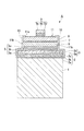
図1に示す発光ダイオードAは、基体となるメッキ層1と、メッキ層1上に配置されたシード層2と、シード層2の上に配置されたバリア層3と、バリア層3上に配置された反射性p型電極5と、反射性p型電極5上に配置された積層半導体層11と、積層半導体層11上に配置されたn型電極9と、から概略構成されている。"Light Emitting Diode"
A light-emitting diode A shown in FIG. 1 includes a
n型電極9は、積層半導体層11のn型半導体層8とオーミック接触することによって、積層半導体層11の負極となっている。図1に示すn型電極9は、n型半導体層8に接するCr膜9aと、Cr膜9aに積層されたTi膜9bと、Ti膜9bに積層されたAu膜9cとからなる3層構造とされている。n型電極9はこの3層構造に限らず、Ti膜、Al膜、Ti膜及びAu膜が積層されてなる4層構造でもよい。
このn型電極9は、後述するように、光取出面11aをドライエッチングした後にCr膜9a、Ti膜9b及びAu膜9cを順次積層することによって形成され、これによりアニール処理を施すことなくn型半導体層8との間でオーミック接触が得られるようになっている。The n-
As will be described later, the n-
ここで反射性p型電極5は、バリア層3及びシード層2を介してメッキ層1と電気的に接続されており、これによりメッキ層1が反射性p型電極5の取出電極となっている。また、反射性p型電極5及びメッキ層1と、n型電極9とは、積層半導体層11の厚み方向両側に配置された関係になっている。これにより本実施形態の発光ダイオードAは、所謂上下電極構造の発光ダイオードとなっている。
Here, the reflective p-
次に積層半導体層11は、p型半導体層6、発光層7及びn型半導体層8が積層されて構成されている。積層半導体層11の上面は、発光層7からの光を外部に取り出す光取出面11aとされており、この光取出面11a上にはn型電極9が形成されている。また、光取出面11aはエッチング等の手段によって粗面化されており、これにより発光ダイオードAの光取出効率がより高められている。
Next, the
更に、積層半導体層11の側面11bと光取り出し面11aの外周部分とには、例えばSiO2等の絶縁性材料からなる保護用の絶縁膜10が形成されている。この絶縁膜10は、反射性p型電極5、バリア層3及びシード層2の側面まで延在されている。絶縁膜10を形成することによって、例えば積層半導体層11の側面11bに異物が付着した場合でも、異物によるn型半導体層8とp型半導体層7との短絡が防止される。Further, a protective insulating
また図1に示すように、積層半導体層11の下側には、反射性p型電極5が配置されている。反射性p型電極5は、積層半導体層11のp型半導体層6とオーミック接触することによって、積層半導体層11の正極となっている。
また、反射性p型電極5は、図1に示すように、積層半導体層11に接するオーミックコンタクト層5cと、オーミックコンタクト層5cに接する反射層5bと、反射層5bに接する相互拡散防止層5aとから構成されている。反射層5bを備えることによって反射性p型電極5は、発光層7から発した光を光取出面11a側に反射させる反射層となっている。
この反射性p型電極5は、後述するように、オーミックコンタクト層5cをRFスパッタリング法を用いて積層し、反射層5b及び相互拡散防止層5aは例えばDCスパッタリング法を用いて積層することによって形成され、これによりアニール処理を施すことなく積層半導体層11との間でオーミック接触が得られるようになっている。As shown in FIG. 1, a reflective p-
As shown in FIG. 1, the reflective p-
As will be described later, the reflective p-
オーミックコンタクト層5cに要求される性能としては、p型半導体層6との接触抵抗が小さいことが必須である。オーミックコンタクト層5cの材料はp型半導体層6との接触抵抗の観点から、Pt、Ru、Os、Rh、Ir、Pd等の白金族またはAgが好ましく、Pt,Ir,RhまたはRuがより好ましく、Ptが特に好ましい。Agを用いることは良好な反射を得るためには好ましいが、接触抵抗はPtよりも低い。したがって、接触抵抗がそれほど要求されない用途にはAgを用いることも可能である。オーミックコンタクト層5cの厚さは、低接触抵抗を安定して得るために0.1nm以上とすることが好ましい。さらに好ましくは1nm以上であり、均一な接触抵抗が得られる。
As the performance required for the
オーミックコンタクト層5cには、Ag合金、Al合金などの反射層5bが積層されている。Pt,Ir,Rh,Ru,OS,PdなどはAg合金と比較すると可視光から紫外領域の反射率が低い。したがって、発光層7からの光が十分に反射せずに出力の高い素子を得ることが難しい。この場合、オーミックコンタクト層5cを光が十分に透過するほどに薄く形成し、Ag合金などの反射層5bを形成して反射光を得る方が、良好なオーミック接触が得られ、かつ出力の高い素子を作成することができる。この場合、オーミックコンタクト層5cの膜厚は30nm以下とすることが好ましい。さらに好ましくは10nm以下である。反射層5bの膜厚は良好な反射率を得るために0.1nm以上とすることが好ましい。さらに好ましくは1nm以上であり、均一な密着性が得られる。Ag合金はマイグレーションを起こしやすいので薄い方が好ましい。したがって、膜厚は200nm以下にすることが好ましい。
A reflective layer 5b such as an Ag alloy or an Al alloy is laminated on the
相互拡散防止層5aは、反射層5bの構成元素と、後述するバリア層3の構成元素との相互拡散を防止するために形成される。相互拡散防止層5aとしては、例えば、Pt等を用いることが好ましい。
The
次に図1に示すように、反射性p型電極5の下側にはバリア層3が配置されている。バリア層3は、後述するように、サファイア基板上に積層半導体層11を形成した後、積層半導体層11に分割溝をドライエッチング等で設ける際のバリアとなる層であって、Ni膜3bとAu膜3aとの積層膜で構成されている。Ni膜3bの厚みは、例えば20〜200nm程度がよく、Au膜3aの厚みは、例えば50〜300nm程度がよい。また、バリア層3全体の厚みは、例えば70〜500nm程度がよい。
このバリア層3は、発光ダイオードAの構成部材として必ずしも必須な積層膜ではなく、シード層2や反射性p型電極5にバリア機能を持たせることができれば、バリア層3は省略してもよい。Next, as shown in FIG. 1, the
The
次に図1に示すように、バリア層3の下側には、シード層2が配置されている。シード層2は、メッキ層1をメッキ法によって形成する際の下地になる層であって、Ti膜2cとTa膜2bとCu膜2aとの積層膜で構成されている。また、シード層2は、Cuからなる単層膜としてもよい。Ti膜2cの厚みは、例えば100〜300nm程度がよく、Ta膜2bの厚みは、例えば200〜700nm程度がよく、Cu膜2aの厚みは、例えば100〜500nm程度がよい。また、シード層2全体の厚みは、例えば400〜1500nm程度がよい。ここでTa膜2bは、Cuのバリアとして機能する。
このシード層2は、発光ダイオードAの構成部材として必ずしも必須な積層膜ではなく、バリア層3や反射性p型電極5にメッキの下地層としての機能を持たせることができれば、シード層2は省略してもよい。Next, as shown in FIG. 1, the
The
次に、メッキ層1は、シード層2を下地として例えば電気メッキ法により形成される金属層である。メッキ層1の材質は、シード層2の材質に対応するものが好ましく、本実施形態ではメッキ層1として、シード層2のCu膜2aと同じ材質であるCuが好ましい。
またCuは、電気抵抗が低く熱伝導性が高い点においても上下電極構造の発光ダイオードAの基体の材質として好ましい。メッキ層1の厚みは、例えば150μm程度がよい。メッキ層1を備えることによって、発光ダイオードAの放熱効率が高められる。Next, the
Cu is also preferable as the material of the base of the light emitting diode A having the upper and lower electrode structure from the viewpoint of low electric resistance and high thermal conductivity. The thickness of the
次に、積層半導体層11は、p型半導体層6と発光層7とn型半導体層8とから概略構成されている。
積層半導体層11としては、GaN系単結晶、GaP系単結晶、GaAs系単結晶、ZnO系単結晶など周知の半導体発光材料を用いることができるが、後述するサファイア単結晶またはSiC単結晶からなる基板に対してエピタキシャル成長可能な点において、GaN系単結晶またはZnO系単結晶がより好ましく、GaN系単結晶が更に好ましい。Next, the
As the stacked
GaN系単結晶からなる半導体層としては、例えば一般式AlXGaYInZN1-AMA(0≦X≦1、0≦Y≦1、0≦Z≦1で且つ、X+Y+Z=1。記号Mは窒素(N)とは別の第V族元素を表し、0≦A<1である。)で表わされるGaN系半導体が多数知られており、本発明においても、それら周知のGaN系半導体を含めて一般式AlXGaYInZN1-AMA(0≦X≦1、0≦Y≦1、0≦Z≦1で且つ、X+Y+Z=1。記号Mは窒素(N)とは別の第V族元素を表し、0≦A<1である。)で表わされるGaN系半導体を何ら制限なく用いることができる。As the semiconductor layer made of GaN based single crystal, for example, and by the general formula Al X Ga Y In Z N 1 -A M A (0 ≦ X ≦ 1,0 ≦ Y ≦ 1,0 ≦ Z ≦ 1, X + Y + Z = 1 The symbol M represents a group V element different from nitrogen (N), and 0 ≦ A <1.) There are many known GaN-based semiconductors, and these well-known GaN are also used in the present invention. Including general semiconductors Al X Ga Y In Z N 1-A M A (0 ≦ X ≦ 1, 0 ≦ Y ≦ 1, 0 ≦ Z ≦ 1, and X + Y + Z = 1. Symbol M represents nitrogen (N ) Represents another group V element, and 0 ≦ A <1.) A GaN-based semiconductor represented by the above can be used without any limitation.
n型半導体層8は、下地層と、nコンタクト層と、発光層7に接するnクラッド層とが積層されて構成される。nコンタクト層は下地層および/またはnクラッド層を兼ねることができる。
下地層はAlXGa1―XN層(0≦x≦1、好ましくは0≦x≦0.5、さらに好ましくは0≦x≦0.1)から構成されることが好ましい。その膜厚は0.1μm以上、好ましくは0.5μm以上、さらに好ましくは1μm以上である。この膜厚以上にした方が結晶性の良好なAlXGa1―XN層が得られやすい。
下地層にはn型不純物を1×10¹⁷〜1×10¹⁹/cm3の範囲内であればドープしても良いが、アンドープ(<1×1017/cm3)の方が良好な結晶性の維持という点で好ましい。n型不純物としては、特に限定されないが、例えば、Si、GeおよびSn等が挙げられ、好ましくはSiおよびGeであり、より好ましくはSiである。The n-
Underlayer Al X Ga 1-X N layer (0 ≦ x ≦ 1, preferably 0 ≦ x ≦ 0.5, and more preferably 0 ≦ x ≦ 0.1) is preferably configured from. The film thickness is 0.1 μm or more, preferably 0.5 μm or more, more preferably 1 μm or more. When the thickness is larger than this, an AlxGa1-XN layer with good crystallinity is easily obtained.
The underlayer may be doped with n-type impurities within the range of 1 × 10 17 to 1 × 10 19 / cm 3 , but undoped (<1 × 10 17 / cm 3 ) is a better crystal. It is preferable in terms of maintaining the property. Although it does not specifically limit as an n-type impurity, For example, Si, Ge, Sn, etc. are mentioned, Preferably it is Si and Ge, More preferably, it is Si.
nコンタクト層としては、下地層と同様にAlXGa1―XN層(0≦x≦1、好ましくは0≦x≦0.5、さらに好ましくは0≦x≦0.1)から構成されることが好ましい。
また、nコンタクト層にはn型不純物がドープされていることが好ましく、n型不純物を1×10¹⁷〜1×10¹⁹/cm3、好ましくは1×1018〜1×1019/cm3の濃度で含有すると、n型電極9との良好なオーミック接触の維持、クラック発生の抑制、良好な結晶性の維持の点で好ましい。n型不純物としては、特に限定されないが、例えば、Si、GeおよびSn等が挙げられ、好ましくはSiおよびGeであり、より好ましくはSiである。
nコンタクト層を構成するGaN系半導体は、下地層と同一組成であることが好ましく、nコンタクト層と下地層との合計の膜厚を1〜20μm、好ましくは2〜15μm、さらに好ましくは3〜12μmの範囲に設定することが好ましい。nコンタクト層と下地層との合計の膜厚が上記範囲にあると、半導体の結晶性が良好に維持される。The n contact layer is composed of an Al x Ga 1-x N layer (0 ≦ x ≦ 1, preferably 0 ≦ x ≦ 0.5, more preferably 0 ≦ x ≦ 0.1), as in the case of the base layer. It is preferable.
The n contact layer is preferably doped with an n-type impurity, and the n-type impurity is preferably 1 × 10 17 to 1 × 10 19 / cm 3 , preferably 1 × 10 18 to 1 × 10 19 / cm 3. If it contains at the density | concentration, it is preferable at the point of maintenance of favorable ohmic contact with the n-
The GaN-based semiconductor constituting the n contact layer preferably has the same composition as that of the base layer, and the total film thickness of the n contact layer and the base layer is 1 to 20 μm, preferably 2 to 15 μm, more preferably 3 to 3. It is preferable to set in the range of 12 μm. When the total film thickness of the n-contact layer and the underlayer is in the above range, the crystallinity of the semiconductor is favorably maintained.
nコンタクト層と発光層7との間には、nクラッド層を設けることが好ましい。nコンタクト層の表面に生じた平坦性の悪化を埋めることできるからである。nクラッド層はAlGaN、GaN、GaInNなどで形成することが可能である。また、これらの構造のヘテロ接合や複数回積層した超格子構造としてもよい。nクラッド層をGaInNで形成する場合には、発光層7のGaInNのバンドギャップよりも大きくすることが望ましいことは言うまでもない。
nクラッド層の膜厚は、特に限定されないが、好ましくは0.005〜0.5μmであり、より好ましくは0.005〜0.1μmである。nクラッド層のn型ドープ濃度は1×10¹⁷〜1×10²⁰/cm3が好ましく、より好ましくは1×1018〜1×1019/cm3である。ドープ濃度がこの範囲であると、良好な結晶性の維持および素子の動作電圧低減の点で好ましい。It is preferable to provide an n clad layer between the n contact layer and the
The thickness of the n-clad layer is not particularly limited, but is preferably 0.005 to 0.5 μm, more preferably 0.005 to 0.1 μm. The n-type doping concentration of the n-clad layer is preferably 1 × 10 17 to 1 × 10 20 / cm 3 , more preferably 1 × 10 18 to 1 × 10 19 / cm 3 . A doping concentration within this range is preferable in terms of maintaining good crystallinity and reducing the operating voltage of the device.
次に、n型半導体層8の下側に積層される発光層7としては、GaN系半導体、好ましくはGa1-sInsN(0<s<0.4)のGaN系半導体からなる発光層が本発明では通常用いられる。発光層7の膜厚としては、特に限定されないが、量子効果の得られる程度の膜厚、即ち臨界膜厚が挙げられ、例えば好ましくは1〜10nmであり、より好ましくは2〜6nmである。発光層7の膜厚が上記範囲であると発光出力の点で好ましい。
また、発光層7は、上記のような単一量子井戸(SQW)構造の他に、上記Ga1-sInsNを井戸層として、この井戸層よりバンドギャップエネルギーが大きいAlcGa1-cN(0≦c<0.3)障壁層とからなる多重量子井戸(MQW)構造としてもよい。また、井戸層および障壁層には、不純物をドープしてもよい。Next, as the
In addition to the single quantum well (SQW) structure as described above, the
次に、p型半導体層6は、発光層7に接するpクラッド層と、pコンタクト層とが積層されて構成される。しかし、pコンタクト層がpクラッド層を兼ねてもよい。
pクラッド層としては、発光層7のバンドギャップエネルギーより大きくなる組成であり、発光層7へのキャリアの閉じ込めができるものであれば特に限定されないが、好ましくは、AldGa1-dN(0<d≦0.4、好ましくは0.1≦d≦0.3)のものが挙げられる。pクラッド層が、このようなAlGaNからなると、発光層7へのキャリアの閉じ込めの点で好ましい。pクラッド層の膜厚は、特に限定されないが、好ましくは1〜400nmであり、より好ましくは5〜100nmである。pクラッド層のp型ドープ濃度は、1×10¹⁸〜1×10²¹/cm3が好ましく、より好ましくは1×1019〜1×1020/cm3である。p型ドープ濃度が上記範囲であると、結晶性を低下させることなく良好なp型結晶が得られる。Next, the p-
The p-cladding layer is not particularly limited as long as it has a composition larger than the band gap energy of the light-emitting
pコンタクト層は、少なくともAleGa1-eN(0≦e<0.5、好ましくは0≦e≦0.2、より好ましくは0≦e≦0.1)を含んでなるGaN系半導体層である。Al組成が上記範囲であると、良好な結晶性の維持および反射性p型電極5との良好なオーミック接触の点で好ましい。p型不純物(ドーパント)を1×10¹⁸〜1×10²¹/cm3の濃度で、好ましくは5×1019〜5×1020/cm3の濃度で含有していると、良好なオーミック接触の維持、クラック発生の防止、良好な結晶性の維持の点で好ましい。p型不純物としては、特に限定されないが、例えば好ましくはMgが挙げられる。膜厚は、特に限定されないが、0.01〜0.5μmが好ましく、より好ましくは0.05〜0.2μmである。膜厚がこの範囲であると、発光出力の点で好ましい。The p-contact layer includes at least Al e Ga 1-e N (0 ≦ e <0.5, preferably 0 ≦ e ≦ 0.2, more preferably 0 ≦ e ≦ 0.1). Is a layer. An Al composition within the above range is preferable in terms of maintaining good crystallinity and good ohmic contact with the reflective p-
『発光ダイオードの製造方法』
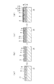
次に、図2〜図5を参照して、発光ダイオードAの製造方法について説明する。本実施形態の発光ダイオードAの製造方法は、基板21上に積層半導体層11を形成するとともに反射性p型電極5を形成する積層工程と、シード層2を形成するとともにシード層2上にメッキ層1を形成するメッキ工程と、基板21を取り除く除去工程と、積層半導体層11の光取出面側に分割溝を形成する分割工程と、積層半導体層11の分割面に保護用の絶縁膜10を形成する絶縁膜形成工程と、n型半導体層8の光取出面11aを粗面化する粗面化工程と、n型半導体層8の光取出面11aにドライエッチングを施してからn型電極9を形成する電極形成工程と、メッキ層1に別の分割溝を設けるとともに分離溝と別の分離溝とに沿ってシード層2を切断するダイシング工程と、から構成されている。
以下、各工程について図面を参照しつつ説明する。"Manufacturing method of light emitting diode"
Next, with reference to FIGS. 2-5, the manufacturing method of the light emitting diode A is demonstrated. The manufacturing method of the light emitting diode A according to the present embodiment includes a stacking process in which the stacked
Hereinafter, each process will be described with reference to the drawings.
「積層工程」
積層工程では、図2(a)〜図2(b)に示すように、基板21上に、n型半導体層8、発光層7及びp型半導体層6を順次積層して積層半導体層11を形成するとともに、p型半導体層6上に、素子となる単位毎に複数の反射性p型電極5を形成する。"Lamination process"
In the stacking step, as shown in FIGS. 2A to 2B, the n-
具体的には、まず図2(a)に示すように、基板21上に、n型半導体層8、発光層7及びp型半導体層6を順次積層して積層半導体層11を形成する。
また、n型半導体層8にはn型ドーパントとしてSi等をドープさせることが望ましく、p型半導体層6にはp型ドーパントとしてMg等をドープさせることが望ましい。
更に、基板21上に積層半導体層11を形成する際には、あらかじめ基板21上にバッファ層を形成することが望ましい。すなわち、基板21としてサファイア基板を用い、n型半導体層8としてGaNを形成する場合には、基板21とn型半導体層8との格子定数が10%以上も異なる。この場合に、バッファ層として、基板21とn型半導体層8との中間の格子定数を有するAlNやAlGaNなどを用いることで、n型半導体層8を構成するGaNの結晶性を向上させることができる。Specifically, first, as shown in FIG. 2A, an n-
The n-
Further, when forming the
そして、バッファ層上に、n型半導体層8、発光層7及びp型半導体層6を順次積層して積層半導体層11を形成する。積層半導体層11の成長方法は特に限定されず、スパッタリング法、MOCVD(有機金属化学気相成長法)、HVPE(ハイドライド気相成長法)、MBE(分子線エピタキシー法)、などGaN系半導体を成長させることが知られている全ての方法を適用できる。好ましい成長方法としては、膜厚制御性、量産性の観点からスパッタリング法またはMOCVD法である。
Then, the stacked
スパッタリング法では、Gaを含むターゲットを用いるとともに、プラズマガスとしてアルゴンと窒素の混合ガスを用いて、所謂リアクティブスパッタリング法によってGaN系半導体を形成することが好ましい。
また、MOCVD法では、キャリアガスとして水素(H2)または窒素(N2)、III族原料であるGa源としてトリメチルガリウム(TMG)またはトリエチルガリウム(TEG)、Al源としてトリメチルアルミニウム(TMA)またはトリエチルアルミニウム(TEA)、In源としてトリメチルインジウム(TMI)またはトリエチルインジウム(TEI)、V族原料であるN源としてアンモニア(NH3)、ヒドラジン(N2H4)などが用いられる。また、ドーパントとしては、n型にはSi原料としてモノシラン(SiH4)またはジシラン(Si2H6)を、Ge原料としてゲルマンガス(GeH4)や、テトラメチルゲルマニウム((CH3)4Ge)やテトラエチルゲルマニウム((C2H5)4Ge)等の有機ゲルマニウム化合物を利用できる。
MBE法では、元素状のゲルマニウムもドーピング源として利用できる。p型にはMg原料としては例えばビスシクロペンタジエニルマグネシウム(Cp2Mg)またはビスエチルシクロペンタジエニルマグネシウム(EtCp2Mg)を用いればよい。In the sputtering method, it is preferable to form a GaN-based semiconductor by a so-called reactive sputtering method using a target containing Ga and using a mixed gas of argon and nitrogen as a plasma gas.
In the MOCVD method, hydrogen (H 2 ) or nitrogen (N 2 ) is used as a carrier gas, trimethyl gallium (TMG) or triethyl gallium (TEG) is used as a Ga source which is a group III material, trimethyl aluminum (TMA) is used as an Al source, or Triethylaluminum (TEA), trimethylindium (TMI) or triethylindium (TEI) as an In source, ammonia (NH 3 ), hydrazine (N 2 H 4 ), or the like as an N source that is a group V material are used. In addition, as a dopant, for n-type, monosilane (SiH 4 ) or disilane (Si 2 H 6 ) is used as a Si raw material, germanium gas (GeH 4 ) or tetramethyl germanium ((CH 3 ) 4 Ge) is used as a Ge raw material. And an organic germanium compound such as tetraethylgermanium ((C 2 H 5 ) 4 Ge) can be used.
In the MBE method, elemental germanium can also be used as a doping source. For the p-type, for example, biscyclopentadienyl magnesium (Cp 2 Mg) or bisethylcyclopentadienyl magnesium (EtCp 2 Mg) may be used as the Mg raw material.
次に、図2(b)に示すように、積層半導体層11のp型半導体層6上に、オーミックコンタクト層、反射層及び密着層を順次積層し、次いで、フォトリソグラフィ技術によってパターニングすることにより、反射性p型電極5を形成する。
Next, as shown in FIG. 2B, an ohmic contact layer, a reflective layer, and an adhesion layer are sequentially stacked on the p-
オーミックコンタクト層をp型半導体層6上に形成するにあたり、RF放電によるスパッタリング成膜法で形成することが好ましい。RF放電によるスパッタリング成膜法を用いることで、蒸着法やDC放電のスパッタリング成膜法を用いるより接触抵抗の低い電極を形成できる。即ち、RF放電によるスパッタリング成膜法でオーミックコンタクト層を形成することによって、オーミックコンタクト層にp型半導体層6の構成元素が混在し、p型半導体層6にはオーミックコンタクト層の構成元素が混在することになり、これによりオーミックコンタクト層とp型半導体層6とがオーミック接合される。
In forming the ohmic contact layer on the p-
RF放電によるスパッタリング成膜では、イオンアシスト効果により、p型半導体層6に付着したスパッタ原子にエネルギーを与え、p型半導体、例えばMgドープのp−GaNとの間で表面拡散を促す作用があると考えられる。さらに、上記成膜においては、p型半導体層6の最表面原子にもエネルギーを与え、半導体材料、例えばGaがオーミックコンタクト層に拡散することを促す作用もあると考えられる。
In sputtering film formation by RF discharge, energy is given to sputtered atoms attached to the p-
RF放電による成膜では、初期において、接触抵抗を下げる効果を持つが、膜厚を大きくすると、その膜が疎であるために反射率の点ではDC放電による成膜に比べて劣る。そこで、接触抵抗を低く保った範囲で薄膜化して光透過率を上げたオーミックコンタクト層をRF放電により形成し、その上に反射層及び相互拡散防止層をDC放電により形成することが好ましい。 The film formation by RF discharge has an effect of lowering the contact resistance in the initial stage. However, when the film thickness is increased, the film is sparse, so that the reflectivity is inferior to the film formation by DC discharge. Therefore, it is preferable to form an ohmic contact layer that is thinned and increases the light transmittance within a range in which contact resistance is kept low by RF discharge, and a reflective layer and an interdiffusion prevention layer are formed thereon by DC discharge.
上記の如く、オーミックコンタクト層をRFスパッタリング法により形成することによって、オーミックコンタクト層とp型半導体層6とをオーミック接触させることができる。この場合、オーミックコンタクト層形成後のアニールを必要としない。むしろ、アニールすることにより、Pt、Gaそれぞれの拡散を促進し、半導体の結晶性を下げてしまうため、電気特性を悪化させてしまうことがあるので好ましくない。従ってオーミックコンタクト層形成後、350℃よりも高い温度で熱処理されていないことが好ましい。
As described above, the ohmic contact layer and the p-
スパッタリングは、従来公知のスパッタリング装置を用いて従来公知の条件を適宜選択して実施することができる。積層半導体層11を積層した基板21をチャンバ内に収容し、基板温度を室温から500℃の範囲に設定する。基板加熱は特に必要としないが、オーミックコンタクト層の構成元素およびp型半導体層6の構成元素の拡散を促進するために適度に加熱しても良い。チャンバ内は真空度が10-4〜10-7Paとなるまで排気する。
スパッタリング用ガスとしては、He、Ne、Ar、Kr、Xe等が使用できる。入手の容易さからArとするのが望ましい。これらの内の一つのガスをチャンバ内に導入し、0.1〜10Paにしたのち放電を行う。好ましくは0.2〜5Paの範囲に設定する。供給する電力は0.2〜2.0kWの範囲が好ましい。この際、放電時間と供給電力を調節することによって、形成する層の厚さを調節することができる。
オーミックコンタクト層をp型半導体層6上に形成するにあたり、真空蒸着法により形成しても同等の効果が得られる。Sputtering can be carried out by appropriately selecting conventionally known conditions using a conventionally known sputtering apparatus. The
As the sputtering gas, He, Ne, Ar, Kr, Xe, or the like can be used. Ar is desirable because of availability. One of these gases is introduced into the chamber and the discharge is performed after the pressure is set to 0.1 to 10 Pa. Preferably it sets to the range of 0.2-5Pa. The supplied power is preferably in the range of 0.2 to 2.0 kW. At this time, the thickness of the layer to be formed can be adjusted by adjusting the discharge time and supply power.
When the ohmic contact layer is formed on the p-
「メッキ工程」
次に、メッキ工程では、図2(c)〜図3(b)に示すように、反射性p型電極5及びp型半導体層6を覆うようにバリア層3及びシード層2を形成し、反射性p型電極5同士を相互に隔てる境界部分に沿って分離用フォトレジスト22を形成し、分離用フォトレジスト22を覆うようにシード層2上にメッキ層1を形成する。尚、分離用フォトレジスト材料としては公知のものを使用することができる。"Plating process"
Next, in the plating step, as shown in FIGS. 2C to 3B, the
具体的には図2(c)に示す如く、反射性p型電極5及びp型半導体層6を覆うように、Ni膜とAu膜とを順次積層してバリア層3を形成する。
次に、図2(d)に示す如く、バリア層3を覆うように、Ti膜2cとTa膜2bとCu膜2aとを順次積層してシード層2を形成する。Specifically, as shown in FIG. 2C, a
Next, as shown in FIG. 2D, a
次に、図3(a)に示すように、反射性p型電極5同士を相互に隔てる境界部分に沿って分離用フォトレジスト22を平面視略格子状に形成する。分離用フォトレジスト22は例えば、高さ300μm程度、幅が数十μm程度になるように形成すればよい。
次に図3(b)に示すように、シード層2及び分離用フォトレジスト22を覆うようにメッキ層1を形成する。メッキ層1の形成は、シード層2に電流を印加しつつ電気メッキ法で行うとよい。このときのメッキ層1の厚みは、1.0〜2mm程度にすればよい。Next, as shown in FIG. 3A, a
Next, as shown in FIG. 3B, the
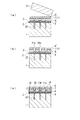
「除去工程」
次に除去工程では、図3(c)〜図4(a)に示すように、n型半導体層8からバッファ層及び基板21を取り除いて、下地層を露出させる。
バッファ層及び基板21を取り除く方法としては、研磨法、エッチング法、レーザリフトオフ法など公知の技術を何ら制限なく用いることが出来るが、本実施形態では生産性の観点からレーザリフトオフ法を用いることが好ましい。
具体的には図3(c)に示すように、バッファ層と基板21との界面近傍にレーザー光Lを照射し、主にバッファ層を熱分解させることによって、図4(a)に示すようにn型半導体層8から基板21を剥離させる。n型半導体層8から基板21及びバッファ層を取り除くことによって、n型半導体層8のバッファ層との接合面が露出される。"Removal process"
Next, in the removing step, as shown in FIGS. 3C to 4A, the buffer layer and the
As a method for removing the buffer layer and the
Specifically, as shown in FIG. 3 (c), the vicinity of the interface between the buffer layer and the
「分割工程」
次に分割工程では、図4(b)に示すように、境界部分の分離用フォトレジスト22に沿って積層半導体層11の光取出面11a側に分割溝11cを形成する。
具体的には図4(b)に示すように、積層半導体層11上にマスクを形成し、ドライエッチング等の手段によって積層半導体層11を格子状にエッチングすることにより、積層半導体層11に平面視略格子状の分離溝11cを設ける。エッチングは、バリア層3が露出した時点で終了する。分離溝11cは、分離用フォトレジスト22とほぼ重なるように形成することが好ましい。このようにして、積層半導体層11が格子状の分割溝11cによって複数に分割される。"Division process"
Next, in the dividing step, as shown in FIG. 4B, a dividing
Specifically, as shown in FIG. 4B, a mask is formed on the
「絶縁膜形成工程」
次に、絶縁膜形成工程では、図4(c)に示すように、分割溝11cによって複数に分割された積層半導体層11の各側面(分割面)11bに、保護用の絶縁膜10を形成する。
具体的には図4(c)に示すように、CVD法やスパッタ法等の手段によって、SiO2からなる絶縁膜10を、各積層半導体層11の側面11bと、各積層半導体層11同士の間に露出するバリア層3と、各積層半導体層11の光取り出し面11aの外周部分を覆うように形成する。積層半導体層11の全体に絶縁膜10を形成し、光取出面11aの中央部以外の部分にレジストを形成し、ドライエッチングすることで、目的の絶縁膜10を形成できる。"Insulating film formation process"
Next, in the insulating film forming step, as shown in FIG. 4C, the protective insulating
Specifically, as shown in FIG. 4C, the insulating
「粗面化工程」
次に、粗面化工程では、n型半導体層8の光取出面11aを粗面化する。
具体的には、加熱KOH溶液に浸漬して、光取出面11aの中央の絶縁膜10に被覆されずに露出している部分の、n型半導体層8を構成する下地層を除去するとともに、n型半導体層8の光取出面11aを粗面化する。
下地層の除去には、PEC(photo electrochemical etch)を使用することもできる。
また、下地層の除去及び光取出面11aの粗面化にはドライエッチングを適用することもできる。
尚、上記の下地層の除去操作は、下地層がアンドープ層である場合に必要な操作であって、下地層にSi等がドープされている場合には下地層の除去操作は不要である。"Roughening process"
Next, in the roughening step, the
Specifically, by immersing in a heated KOH solution, removing the underlying layer constituting the n-
PEC (photo electrochemical etch) can also be used to remove the underlayer.
Also, dry etching can be applied to the removal of the underlayer and the roughening of the
The above-described underlayer removal operation is necessary when the underlayer is an undoped layer, and when the underlayer is doped with Si or the like, the underlayer removal operation is not necessary.
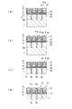
「電極形成工程」
電極形成工程では、図5(a)及び図5(b)に示すように、n型半導体層8の光取出面11aを、n型半導体層8中のドーパント元素と同一の元素を含有するエッチングガスによりドライエッチングしてから、光取出面11aにn型電極9を形成する。
具体的には図5(a)に示すように、メッキ層1、反射性p型電極5及び積層半導体層11等を含むメッキ基板をプラズマドライエッチング装置のチャンバに収納し、n型半導体層8中のドーパント元素と同一の元素を含有するエッチングガスからなる反応ガスをチャンバ内に供給し、積層半導体層11の上方においてプラズマを発生させ、エッチングガスを含むプラズマによって光取出面11aをドライエッチングする。"Electrode formation process"
In the electrode formation step, as shown in FIGS. 5A and 5B, the
Specifically, as shown in FIG. 5A, a plating substrate including a
エッチングガスとしては、n型半導体層8中のドーパント元素がケイ素(Si)の場合は、エッチングガスとしてハロゲン化ケイ素を用いることが好ましく、具体的にはSiCl4またはSiF4が好ましい。
また、反応ガスを導入した際のチャンバ内の圧力は、例えば0.2〜2Paの範囲にすることが好ましく、エッチングガスの流量は15sccm〜50sccmの範囲が好ましく、プラズマのパワーは120W程度が好ましく、バイアスは50W程度が好ましく、処理時間は150秒程度がよい。
さらに、エッチング速度は5nm/分以上100nm/分以下が好ましい。100nm/分を超えると、作製されたオーミックコンタクトの耐熱性が悪くなる傾向がある。さらに好ましくは5nm/分以上40nm/分以下、特に好ましくは5nm/分以上25nm/分以下である。
このようなエッチング処理を行うことによって、n型半導体層8の表面近傍にエッチングガスに含まれるSiが打ち込まれて、表面近傍のSi濃度が高められると考えられる。As the etching gas, when the dopant element in the n-
The pressure in the chamber when the reaction gas is introduced is preferably in the range of 0.2 to 2 Pa, the flow rate of the etching gas is preferably in the range of 15 sccm to 50 sccm, and the plasma power is preferably about 120 W. The bias is preferably about 50 W, and the processing time is preferably about 150 seconds.
Furthermore, the etching rate is preferably 5 nm / min or more and 100 nm / min or less. When it exceeds 100 nm / min, the heat resistance of the produced ohmic contact tends to deteriorate. More preferably, it is 5 nm / min or more and 40 nm / min or less, and particularly preferably 5 nm / min or more and 25 nm / min or less.
By performing such an etching process, it is considered that Si contained in the etching gas is implanted in the vicinity of the surface of the n-
次に、図5(b)に示すように、プラズマ処理後のn型半導体層8の上に、Cr膜、Ti膜及びAu膜を順次積層してn型電極9を形成する。n型電極9はこの3層構造に限らず、Ti膜、Al膜、Ti膜及びAu膜が積層されてなる4層構造でもよい。n型電極9の形成は、例えば、スパッタリング法や蒸着法を用いればよい。
上記の如く、n型半導体層8の表面をプラズマで処理してから、Cr膜またはTi膜等を積層することによって、n型電極9を構成するCr膜またはTi膜とn型半導体層8とをオーミック接触させることができる。この場合、n型電極9の形成後のアニールを必要としない。むしろ、アニールすることによって電気特性を悪化させてしまうことがあるので好ましくない。Next, as shown in FIG. 5B, an n-
As described above, the surface of the n-
「ダイシング工程」
ダイシング工程では、図5(c)〜図5(d)に示すように、分離用フォトレジスト22の一部が露出するまでメッキ層1を研磨するとともに、分離用フォトレジスト22を除去することによってメッキ層1に別の分割溝1bを設け、更に分離溝11cと別の分離溝1bとに沿ってシード層2を切断する。
具体的にはまず、図5(c)に示すように、メッキ層1の積層半導体層11と反対側の面を例えばCMP等で研磨することによって、分離用フォトレジスト22を露出させる。"Dicing process"
In the dicing process, as shown in FIGS. 5C to 5D, the
Specifically, first, as shown in FIG. 5C, the surface of the
次に、分離用フォトレジスト22を溶解除去もしくはアッシング除去して、メッキ層1に別の分離溝1bを形成する。この別の分離溝1bは、先に設けた積層半導体層11の分離溝11cと対応する位置に設けられる。メッキ層1の別の分離溝1bと積層半導体層11の分離溝11cとの間には、シード層2及びバリア層3のみが残存する状態になる。シード層2及びバリア層3の合計厚みは1μm程度になる。
Next, the
そして、図5(d)に示すように、分離溝11cと別の分離溝1bとの間に残存するシード層2及びバリア層3をダイシングすることによって、複数の発光ダイオードAが得られる。
Then, as shown in FIG. 5D, a plurality of light emitting diodes A are obtained by dicing the
尚、ダイシング工程に代えて、分割工程を行ってもよい。すなわち、電極形成工程の後に、図5(c)と同様にして分離用フォトレジスト22の一部が露出するまでメッキ層1を研磨してから、分離用フォトレジスト22を残したまま、機械的応力を印加することによって分割溝11cに沿って積層半導体層11及びメッキ層1を分割することで、複数の発光ダイオードAを得てもよい。
Note that a dividing step may be performed instead of the dicing step. That is, after the electrode formation step, the
以上説明したように、本実施形態の発光ダイオードAの製造方法によれば、n型半導体層8の光取出面11aを、n型半導体層8中のドーパント元素(例えばSi)と同一の元素を含有するエッチングガス(例えばSiCl4、SiF4等)によってドライエッチングしてから、光取出面11aにn型電極9を形成するので、アニール処理を行うことなくn型半導体層8とn型電極9をオーミック接触させることができる。これにより、先に形成した反射性p型電極5の反射率を低下させるおそれがなく、また、積層半導体層11を構成する半導体層同士の熱拡散等を引き起こすおそれもなく、光取出効率並びに発光効率に優れた発光ダイオードAを製造できる。As described above, according to the method for manufacturing the light emitting diode A of the present embodiment, the
また、本実施形態の発光ダイオードAの製造方法によれば、積層半導体層11にメッキ層1を形成し、その後、基板21を除去することによって、n型電極9及び反射性p型電極5によって積層半導体層11が挟まれた所謂上下電極構造の発光ダイオードAを形成することができる。このようにして得られた発光ダイオードAは、Cu等からなるメッキ層1を備えるので、発光に伴って発生した熱を容易に放熱させることができる。
Further, according to the method for manufacturing the light-emitting diode A of the present embodiment, the plated
また、上記の発光ダイオードAの製造方法によれば、シード層2を形成し、シード層2にメッキ層1を形成するので、シード層2を介してメッキ層1を強固に接合させることができ、機械的強度に優れた発光ダイオードAを製造できる。
Moreover, according to the manufacturing method of the light emitting diode A, the
また、上記の発光ダイオードAの製造方法によれば、反射性p型電極5をRFスパッタリング法によって形成するので、アニール処理を行うことなく反射性p型電極5とp型半導体層6をオーミック接触させることができる。これにより、p型半導体層5のドーパント元素であるMgの一部が、アニール処理によって消失するおそれがなく、p型半導体層6のドーパント濃度が均一に保たれ、発光ダイオードAの電流−電圧特性が低下するおそれがない。
In addition, according to the manufacturing method of the light-emitting diode A, the reflective p-
また、上記の発光ダイオードAの製造方法によれば、分離用フォトレジスト22を覆うようにメッキ層1を形成し、その後、分離用フォトレジスト22を除去することによってメッキ層1に別の分割溝1bを設けるので、メッキ層1を分断するためのダイシング操作が不要になる一方、ダイシング操作の対象がシード層2とバリア層3のみになるので、発光ダイオードAの分割を容易に行うことができる。
また、上記の発光ダイオードAの製造方法によれば、分離用フォトレジスト22を覆うようにメッキ層1を形成し、その後、メッキ層1を研磨して分離用フォトレジスト22を露出させ、その後、機械的応力を加えて発光ダイオードAの分割を行ってもよく、これにより、メッキ層1を分断するためのダイシング操作が不要になり、発光ダイオードAの分割を容易に行うことができる。Further, according to the method for manufacturing the light-emitting diode A, the
In addition, according to the method of manufacturing the light emitting diode A, the
以下に、本発明に係る発光ダイオードの製造の実施例について説明するが、本発明はこれらの実施例にのみ限定されるものではない。
(実施例1)
図1に示す発光ダイオードAを以下に示すようにして作成した。
すなわち、サファイアからなる基板上に、AlNからなる厚さ40nmのバッファ層を形成し、バッファ層上に、厚さ2μmのアンドープGaN下地層、厚さ2μmのSiドープn型GaNコンタクト層及び厚さ20nmのn型In0.1Ga0.9Nクラッド層(n型半導体層)、厚さ15nmのSiドープGaN障壁層および厚さ2nmのIn0.2Ga0.8N井戸層を5回積層し、最後に障壁層を設けた多重井戸構造の発光層、厚さ10nmのMgドープp型Al0.1Ga0.9Nクラッド層及び厚さ200nmのMgドープp型Al0.02Ga0.98Nコンタクト層(p型半導体層)を順に積層し、積層半導体層を得た。Examples of manufacturing the light emitting diode according to the present invention will be described below, but the present invention is not limited to these examples.
Example 1
The light emitting diode A shown in FIG. 1 was produced as follows.
That is, a 40 nm thick buffer layer made of AlN is formed on a substrate made of sapphire, an undoped GaN base layer having a thickness of 2 μm, a Si doped n-type GaN contact layer having a thickness of 2 μm, and a thickness are formed on the buffer layer. 5 times of 20 nm n-type In 0.1 Ga 0.9 N cladding layer (n-type semiconductor layer), 15 nm thick Si-doped GaN barrier layer and 2 nm thick In 0.2 Ga 0.8 N well layer Multi-well structure light-emitting layer that is stacked and finally provided with a barrier layer, Mg-doped p-type Al 0.1 Ga 0.9 N cladding layer with a thickness of 10 nm, and Mg-doped p-type Al 0.02 Ga with a thickness of 200 nm 0.98 N contact layers (p-type semiconductor layers) were sequentially stacked to obtain a stacked semiconductor layer.
次いで、p型半導体層上に、厚さ2nmのオーミックコンタクト層、厚さ100nmの反射層及び厚さ50nmの相互拡散防止層を順次積層し、次いで、フォトリソグラフィ技術によってパターニングすることにより、反射性p型電極を形成した。オーミックコンタクト層をp型半導体層上に形成するにあたり、RF放電によるスパッタリング成膜法で形成した。また、反射層及び相互拡散防止層はDCスパッタリング法で形成した。
次に、反射性p型電極及びp型半導体層を覆うように、厚さ100nmのNi膜と厚さ200nmのAu膜とを蒸着法により順次積層してバリア層を形成した。
次に、バリア層上に、厚さ200nmのTi膜と厚さ400nmのTa膜と厚さ300nmのCu膜とをスパッタリング法により順次積層してシード層を形成した。Next, an ohmic contact layer having a thickness of 2 nm, a reflective layer having a thickness of 100 nm, and an anti-diffusion layer having a thickness of 50 nm are sequentially stacked on the p-type semiconductor layer, and then patterned by a photolithography technique. A p-type electrode was formed. In forming the ohmic contact layer on the p-type semiconductor layer, the ohmic contact layer was formed by a sputtering film forming method using RF discharge. The reflection layer and the mutual diffusion prevention layer were formed by DC sputtering.
Next, a barrier layer was formed by sequentially depositing a Ni film having a thickness of 100 nm and an Au film having a thickness of 200 nm so as to cover the reflective p-type electrode and the p-type semiconductor layer.
Next, a 200 nm thick Ti film, a 400 nm thick Ta film, and a 300 nm thick Cu film were sequentially stacked on the barrier layer by a sputtering method to form a seed layer.
次に、反射性p型電極同士を相互に隔てる境界部分に沿って分離用フォトレジストを平面視略格子状に形成した。分離用フォトレジストは、高さ150μm、幅が60μm程度になるように形成した。
次に、シード層に電流を印加しつつ電気メッキ法によって、シード層及び分離用フォトレジストを覆うようにメッキ層を厚さ1.2mm程度に形成した。Next, a separation photoresist was formed in a substantially lattice shape in plan view along a boundary portion separating the reflective p-type electrodes from each other. The separation photoresist was formed to have a height of about 150 μm and a width of about 60 μm.
Next, a plating layer having a thickness of about 1.2 mm was formed by electroplating while applying current to the seed layer so as to cover the seed layer and the separation photoresist.
次に、レーザーリフトオフ法によってn型半導体層からバッファ層及びサファイア基板を取り除いた。
次に、積層半導体層に格子状の分割溝をドライエッチング法によって形成した。エッチングは、バリア層が露出した時点で終了した。分割溝は、分離用フォトレジストとほぼ重なるように形成した。Next, the buffer layer and the sapphire substrate were removed from the n-type semiconductor layer by a laser lift-off method.
Next, lattice-shaped division grooves were formed in the laminated semiconductor layer by a dry etching method. The etching was finished when the barrier layer was exposed. The dividing grooves were formed so as to substantially overlap with the separation photoresist.
次に、分割溝によって複数に分割された積層半導体層の各側面に、厚さ460nmのSiO2からなる絶縁膜をCVD法で形成した。
次に、n型半導体層の光取出面に対して加熱KOH溶液処理を施すことによって、光取出面を粗面化させた。Next, an insulating film made of SiO 2 having a thickness of 460 nm was formed on each side surface of the laminated semiconductor layer divided into a plurality by the dividing grooves by a CVD method.
Next, the light extraction surface was roughened by performing a heated KOH solution treatment on the light extraction surface of the n-type semiconductor layer.
次に、n型半導体層の光取出面に、SiCl4によるドライエッチングを行った。具体的には、積層半導体層を含むメッキ基板をプラズマドライエッチング装置のチャンバに収納し、反応ガスとしてSiCl4ガスをチャンバ内に供給し、積層半導体層の上方においてプラズマを発生させ、光取出面をエッチングした。
反応ガスを導入した際のチャンバ内の圧力を0.5Paに設定し、エッチングガスの流量を30sccmに設定し、プラズマのパワーを120Wに設定し、バイアスを50Wに設定し、処理時間を150秒に設定した。Next, dry etching with SiCl 4 was performed on the light extraction surface of the n-type semiconductor layer. Specifically, a plated substrate including a laminated semiconductor layer is accommodated in a chamber of a plasma dry etching apparatus, SiCl 4 gas is supplied as a reaction gas into the chamber, plasma is generated above the laminated semiconductor layer, and a light extraction surface Was etched.
The pressure in the chamber when the reaction gas is introduced is set to 0.5 Pa, the flow rate of the etching gas is set to 30 sccm, the plasma power is set to 120 W, the bias is set to 50 W, and the processing time is 150 seconds. Set to.
次に、ドライエッチング処理後のn型半導体層の上に、厚さ40nmのCr膜、厚さ100nmのTi膜及び厚さ1000nmのAu膜を蒸着法によって順次積層してn型電極を形成した。 Next, an n-type electrode was formed by sequentially depositing a Cr film having a thickness of 40 nm, a Ti film having a thickness of 100 nm, and an Au film having a thickness of 1000 nm on the n-type semiconductor layer after the dry etching process. .
次に、分離用フォトレジストの一部が露出するまでメッキ層を研磨し、分離用フォトレジストを溶解除去してメッキ層に別の分割溝を設け、更に分離溝と別の分離溝との間のバリア層及びシード層を切断した。
このようにして、1000μm角の実施例1の発光ダイオードを製造した。Next, the plating layer is polished until a part of the separation photoresist is exposed, and the separation photoresist is dissolved and removed to provide another division groove in the plating layer, and between the separation groove and another separation groove. The barrier layer and the seed layer were cut.
In this way, the light-emitting diode of Example 1 having a 1000 μm square was manufactured.
(比較例1)
プラズマ処理を行わなかったこと以外は上記実施例1と同様にして、比較例1の発光ダイオードを製造した。(Comparative Example 1)
A light emitting diode of Comparative Example 1 was manufactured in the same manner as in Example 1 except that the plasma treatment was not performed.
実施例1及び比較例1の発光ダイオードについて、20mAにおけるVfを測定したところ、プラズマ処理を行った実施例1ではVfが3.20Vとなった。一方、プラズマ処理を行なわなかった比較例1ではVfが3.76Vとなり、実施例1よりも0.56V増大した。 When the Vf at 20 mA was measured for the light emitting diodes of Example 1 and Comparative Example 1, Vf was 3.20 V in Example 1 where the plasma treatment was performed. On the other hand, in Comparative Example 1 in which the plasma treatment was not performed, Vf was 3.76 V, which was 0.56 V higher than that in Example 1.
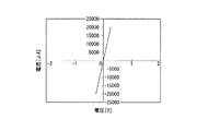
また、実施例1及び比較例1について、n型電極とn型半導体層との間における電流−電圧特性を測定したところ、実施例1では図6に示す通りとなり、比較例1では図7に示す通りとなった。図6から明らかなように、実施例1では電流と電圧との関係が相互に比例する直線関係になり、n型電極とn型半導体層との間でオーミック接合が形成されていることが明らかになった。
一方、図7から明らかなように、比較例1では電流と電圧との関係が直線関係にならず、n型電極とn型半導体層との間でオーミック接合が形成されていないことが明らかになった。
以上説明した通り、n型電極の形成前にプラズマ処理を行うことによって、アニール処理を行うことなく、n型電極とn型半導体層との間でオーミック接合が得られることが明らかになった。Further, for Example 1 and Comparative Example 1, the current-voltage characteristics between the n-type electrode and the n-type semiconductor layer were measured. As a result, Example 1 was as shown in FIG. As shown. As is clear from FIG. 6, in Example 1, the relationship between the current and the voltage is a linear relationship that is proportional to each other, and it is clear that an ohmic junction is formed between the n-type electrode and the n-type semiconductor layer. Became.
On the other hand, as is clear from FIG. 7, in Comparative Example 1, it is clear that the relationship between the current and the voltage is not a linear relationship, and no ohmic junction is formed between the n-type electrode and the n-type semiconductor layer. became.
As described above, it has been clarified that an ohmic junction can be obtained between the n-type electrode and the n-type semiconductor layer without performing the annealing process by performing the plasma treatment before forming the n-type electrode.
本発明によれば、メッキ層を設けることによって上下電極構造を実現して放熱の問題を解消することができる。また、オーミック電極の形成時にアニール処理を必要としないので、発光ダイオードにおけるオーミック電極の劣化や、電流−電圧特性の低下を防止することができる。 According to the present invention, the upper and lower electrode structures can be realized by providing the plating layer, and the problem of heat dissipation can be solved. In addition, since an annealing process is not required when the ohmic electrode is formed, it is possible to prevent the ohmic electrode from deteriorating in the light emitting diode and the current-voltage characteristic from being lowered.
Claims (7)
前記反射性p型電極及び前記p型半導体層を覆うようにシード層を形成した後、前記複数の反射性p型電極を相互に隔てる境界部分に沿って分離用フォトレジストを形成するとともに、前記分離用フォトレジストを覆うように、前記シード層上にメッキ層を形成するメッキ工程と、
前記n型半導体層から前記基板を取り除いて、前記n型半導体層の光取出面を露出させる除去工程と、
前記除去工程の後、前記境界部分の前記分離用フォトレジストに沿って前記積層半導体層の前記光取出面側に分割溝を形成する分割工程と、
前記分割溝を形成する分割工程の後、前記n型半導体層の前記光取出面に、前記n型半導体層中のドーパント元素であるケイ素と同一の元素を含有するハロゲン化ケイ素をエッチングガスに用いてドライエッチングを施してから、前記光取出面にn型電極を形成する電極形成工程と、
前記電極形成工程の後、前記分離用フォトレジストの一部が露出するまで前記メッキ層を研磨するとともに、前記分離用フォトレジストを除去することによって前記メッキ層に別の分割溝を設け、更に前記分離溝と前記別の分離溝とに沿って前記シード層を切断するダイシング工程と、
を具備してなることを特徴とする発光ダイオードの製造方法。 A stacking step of sequentially stacking an n-type semiconductor layer, a light emitting layer, and a p-type semiconductor layer on a substrate to form a stacked semiconductor layer, and forming a plurality of reflective p-type electrodes on the p-type semiconductor layer;
After forming a seed layer so as to cover the reflective p-type electrode and the p-type semiconductor layer, a separation photoresist is formed along a boundary portion separating the plurality of reflective p-type electrodes from each other; A plating step of forming a plating layer on the seed layer so as to cover the separation photoresist ;
Removing the substrate from the n-type semiconductor layer to expose a light extraction surface of the n-type semiconductor layer;
After the removing step, a dividing step of forming a dividing groove on the light extraction surface side of the stacked semiconductor layer along the separation photoresist in the boundary portion;
After the dividing step for forming the dividing groove , silicon halide containing the same element as silicon as a dopant element in the n-type semiconductor layer is used as an etching gas on the light extraction surface of the n-type semiconductor layer. Forming an n-type electrode on the light extraction surface after performing dry etching,
After the electrode forming step, the plating layer is polished until a part of the separation photoresist is exposed, and another separation groove is provided in the plating layer by removing the separation photoresist. A dicing step of cutting the seed layer along a separation groove and the another separation groove;
A method for manufacturing a light emitting diode, comprising:
前記反射性p型電極及び前記p型半導体層を覆うようにシード層を形成した後、前記複数の反射性p型電極を相互に隔てる境界部分に沿って分離用フォトレジストを形成するとともに、前記分離用フォトレジストを覆うように、前記シード層上にメッキ層を形成するメッキ工程と、
前記n型半導体層から前記基板を取り除いて、前記n型半導体層の光取出面を露出させる除去工程と、
前記除去工程の後、前記境界部分の前記分離用フォトレジストに沿って前記積層半導体層の前記光取出面側に分割溝を形成する分割工程と、
前記分割溝を形成する分割工程の後、前記n型半導体層の前記光取出面に、前記n型半導体層中のドーパント元素であるケイ素と同一の元素を含有するハロゲン化ケイ素をエッチングガスに用いてドライエッチングを施してから、前記光取出面にn型電極を形成する電極形成工程と、
前記電極形成工程の後、前記分離用フォトレジストの一部が露出するまで前記メッキ層を研磨してから、機械的応力を印加することによって前記分割溝に沿って前記積層半導体層及び前記メッキ層を分割する分割工程と、
を具備してなることを特徴とする発光ダイオードの製造方法。 A stacking step of sequentially stacking an n-type semiconductor layer, a light emitting layer, and a p-type semiconductor layer on a substrate to form a stacked semiconductor layer, and forming a plurality of reflective p-type electrodes on the p-type semiconductor layer;
After forming a seed layer so as to cover the reflective p-type electrode and the p-type semiconductor layer, a separation photoresist is formed along a boundary portion separating the plurality of reflective p-type electrodes from each other; A plating step of forming a plating layer on the seed layer so as to cover the separation photoresist ;
Removing the substrate from the n-type semiconductor layer to expose a light extraction surface of the n-type semiconductor layer;
After the removing step, a dividing step of forming a dividing groove on the light extraction surface side of the stacked semiconductor layer along the separation photoresist in the boundary portion;
After the dividing step for forming the dividing groove , silicon halide containing the same element as silicon as a dopant element in the n-type semiconductor layer is used as an etching gas on the light extraction surface of the n-type semiconductor layer. Forming an n-type electrode on the light extraction surface after performing dry etching,
After the electrode forming step, the plated layer is polished until a part of the separation photoresist is exposed, and then mechanical stress is applied to the laminated semiconductor layer and the plated layer along the dividing groove. Dividing step of dividing
A method for manufacturing a light emitting diode, comprising:
Priority Applications (1)
| Application Number | Priority Date | Filing Date | Title |
|---|---|---|---|
| JP2009521598A JP5278317B2 (en) | 2007-06-29 | 2008-06-26 | Manufacturing method of light emitting diode |
Applications Claiming Priority (4)
| Application Number | Priority Date | Filing Date | Title |
|---|---|---|---|
| JP2007171920 | 2007-06-29 | ||
| JP2007171920 | 2007-06-29 | ||
| JP2009521598A JP5278317B2 (en) | 2007-06-29 | 2008-06-26 | Manufacturing method of light emitting diode |
| PCT/JP2008/061654 WO2009004980A1 (en) | 2007-06-29 | 2008-06-26 | Method for manufacturing light emitting diode |
Publications (2)
| Publication Number | Publication Date |
|---|---|
| JPWO2009004980A1 JPWO2009004980A1 (en) | 2010-08-26 |
| JP5278317B2 true JP5278317B2 (en) | 2013-09-04 |
Family
ID=40226027
Family Applications (1)
| Application Number | Title | Priority Date | Filing Date |
|---|---|---|---|
| JP2009521598A Active JP5278317B2 (en) | 2007-06-29 | 2008-06-26 | Manufacturing method of light emitting diode |
Country Status (4)
| Country | Link |
|---|---|
| US (1) | US8097478B2 (en) |
| JP (1) | JP5278317B2 (en) |
| TW (1) | TWI360896B (en) |
| WO (1) | WO2009004980A1 (en) |
Families Citing this family (75)
| Publication number | Priority date | Publication date | Assignee | Title |
|---|---|---|---|---|
| KR101449030B1 (en) * | 2008-04-05 | 2014-10-08 | 엘지이노텍 주식회사 | group 3 nitride-based semiconductor light emitting diodes and methods to fabricate them |
| KR101363022B1 (en) * | 2008-12-23 | 2014-02-14 | 삼성디스플레이 주식회사 | Organic light emitting diode display |
| KR100974776B1 (en) * | 2009-02-10 | 2010-08-06 | 엘지이노텍 주식회사 | Light emitting device |
| JP2011029574A (en) * | 2009-03-31 | 2011-02-10 | Toyoda Gosei Co Ltd | Method for producing group iii nitride-based compound semiconductor device |
| JP2011035017A (en) * | 2009-07-30 | 2011-02-17 | Hitachi Cable Ltd | Light-emitting device |
| KR101072034B1 (en) | 2009-10-15 | 2011-10-10 | 엘지이노텍 주식회사 | Semiconductor light emitting device and fabrication method thereof |
| KR101014013B1 (en) * | 2009-10-15 | 2011-02-10 | 엘지이노텍 주식회사 | Semiconductor light emitting device and fabrication method thereof |
| KR101081193B1 (en) | 2009-10-15 | 2011-11-07 | 엘지이노텍 주식회사 | Semiconductor light emitting device and fabrication method thereof |
| JP5423390B2 (en) * | 2009-12-26 | 2014-02-19 | 豊田合成株式会社 | Group III nitride compound semiconductor device and method for manufacturing the same |
| JP5185308B2 (en) | 2010-03-09 | 2013-04-17 | 株式会社東芝 | Manufacturing method of semiconductor light emitting device |
| JP5531794B2 (en) | 2010-06-09 | 2014-06-25 | 日亜化学工業株式会社 | Manufacturing method of semiconductor light emitting device |
| CN102064146A (en) * | 2010-12-03 | 2011-05-18 | 北京大学 | Cooling structure of chip |
| KR101752663B1 (en) * | 2010-12-22 | 2017-06-30 | 엘지이노텍 주식회사 | Light emitting device and method for manufacturing light emitting device |
| US9496454B2 (en) * | 2011-03-22 | 2016-11-15 | Micron Technology, Inc. | Solid state optoelectronic device with plated support substrate |
| US8646505B2 (en) | 2011-11-18 | 2014-02-11 | LuxVue Technology Corporation | Micro device transfer head |
| US8518204B2 (en) | 2011-11-18 | 2013-08-27 | LuxVue Technology Corporation | Method of fabricating and transferring a micro device and an array of micro devices utilizing an intermediate electrically conductive bonding layer |
| US8573469B2 (en) | 2011-11-18 | 2013-11-05 | LuxVue Technology Corporation | Method of forming a micro LED structure and array of micro LED structures with an electrically insulating layer |
| US8426227B1 (en) | 2011-11-18 | 2013-04-23 | LuxVue Technology Corporation | Method of forming a micro light emitting diode array |
| US8349116B1 (en) | 2011-11-18 | 2013-01-08 | LuxVue Technology Corporation | Micro device transfer head heater assembly and method of transferring a micro device |
| TW201324863A (en) * | 2011-12-13 | 2013-06-16 | Genesis Photonics Inc | Light emitting diode element and flip-chip light emitting diode package |
| CN105449072A (en) * | 2011-12-20 | 2016-03-30 | 新世纪光电股份有限公司 | Light emitting diode element |
| JP2013157496A (en) * | 2012-01-31 | 2013-08-15 | Sony Corp | Light-emitting element, method of manufacturing the same, and light-emitting device |
| US9773750B2 (en) | 2012-02-09 | 2017-09-26 | Apple Inc. | Method of transferring and bonding an array of micro devices |
| KR101286211B1 (en) * | 2012-02-16 | 2013-07-15 | 고려대학교 산학협력단 | Method of fabricating light emitting device and light emitting device fabricated by using the same |
| TWI528578B (en) * | 2012-03-28 | 2016-04-01 | 鴻海精密工業股份有限公司 | Method for manufacturing light emitting diode |
| US9548332B2 (en) | 2012-04-27 | 2017-01-17 | Apple Inc. | Method of forming a micro LED device with self-aligned metallization stack |
| US9437783B2 (en) * | 2012-05-08 | 2016-09-06 | Cree, Inc. | Light emitting diode (LED) contact structures and process for fabricating the same |
| US9105492B2 (en) | 2012-05-08 | 2015-08-11 | LuxVue Technology Corporation | Compliant micro device transfer head |
| WO2013171632A1 (en) * | 2012-05-17 | 2013-11-21 | Koninklijke Philips N.V. | Method of separating a wafer of semiconductor devices |
| US8415768B1 (en) | 2012-07-06 | 2013-04-09 | LuxVue Technology Corporation | Compliant monopolar micro device transfer head with silicon electrode |
| US8791530B2 (en) | 2012-09-06 | 2014-07-29 | LuxVue Technology Corporation | Compliant micro device transfer head with integrated electrode leads |
| US9162880B2 (en) | 2012-09-07 | 2015-10-20 | LuxVue Technology Corporation | Mass transfer tool |
| US8941215B2 (en) | 2012-09-24 | 2015-01-27 | LuxVue Technology Corporation | Micro device stabilization post |
| US8835940B2 (en) | 2012-09-24 | 2014-09-16 | LuxVue Technology Corporation | Micro device stabilization post |
| US9558721B2 (en) | 2012-10-15 | 2017-01-31 | Apple Inc. | Content-based adaptive refresh schemes for low-power displays |
| US9236815B2 (en) | 2012-12-10 | 2016-01-12 | LuxVue Technology Corporation | Compliant micro device transfer head array with metal electrodes |
| US9105714B2 (en) | 2012-12-11 | 2015-08-11 | LuxVue Technology Corporation | Stabilization structure including sacrificial release layer and staging bollards |
| US9166114B2 (en) | 2012-12-11 | 2015-10-20 | LuxVue Technology Corporation | Stabilization structure including sacrificial release layer and staging cavity |
| US9308649B2 (en) | 2013-02-25 | 2016-04-12 | LuxVue Techonology Corporation | Mass transfer tool manipulator assembly |
| US9095980B2 (en) | 2013-02-25 | 2015-08-04 | LuxVue Technology Corporation | Micro pick up array mount with integrated displacement sensor |
| US8791474B1 (en) | 2013-03-15 | 2014-07-29 | LuxVue Technology Corporation | Light emitting diode display with redundancy scheme |
| US9252375B2 (en) | 2013-03-15 | 2016-02-02 | LuxVue Technology Corporation | Method of fabricating a light emitting diode display with integrated defect detection test |
| US9484504B2 (en) | 2013-05-14 | 2016-11-01 | Apple Inc. | Micro LED with wavelength conversion layer |
| US9217541B2 (en) | 2013-05-14 | 2015-12-22 | LuxVue Technology Corporation | Stabilization structure including shear release posts |
| US9136161B2 (en) | 2013-06-04 | 2015-09-15 | LuxVue Technology Corporation | Micro pick up array with compliant contact |
| CN105683872B (en) | 2013-06-12 | 2020-05-12 | 罗茵尼公司 | Keyboard backlighting with light generating source |
| US8987765B2 (en) | 2013-06-17 | 2015-03-24 | LuxVue Technology Corporation | Reflective bank structure and method for integrating a light emitting device |
| US9111464B2 (en) | 2013-06-18 | 2015-08-18 | LuxVue Technology Corporation | LED display with wavelength conversion layer |
| US8928021B1 (en) | 2013-06-18 | 2015-01-06 | LuxVue Technology Corporation | LED light pipe |
| US9035279B2 (en) | 2013-07-08 | 2015-05-19 | LuxVue Technology Corporation | Micro device with stabilization post |
| US9296111B2 (en) | 2013-07-22 | 2016-03-29 | LuxVue Technology Corporation | Micro pick up array alignment encoder |
| US9087764B2 (en) | 2013-07-26 | 2015-07-21 | LuxVue Technology Corporation | Adhesive wafer bonding with controlled thickness variation |
| US9153548B2 (en) | 2013-09-16 | 2015-10-06 | Lux Vue Technology Corporation | Adhesive wafer bonding with sacrificial spacers for controlled thickness variation |
| DE102013111496A1 (en) * | 2013-10-18 | 2015-04-23 | Osram Opto Semiconductors Gmbh | Method for producing optoelectronic semiconductor components and optoelectronic semiconductor component |
| US9367094B2 (en) | 2013-12-17 | 2016-06-14 | Apple Inc. | Display module and system applications |
| TWI552386B (en) | 2013-12-20 | 2016-10-01 | 新世紀光電股份有限公司 | Semiconductor light emitting structure and semiconductor package structure |
| US9768345B2 (en) | 2013-12-20 | 2017-09-19 | Apple Inc. | LED with current injection confinement trench |
| US9583466B2 (en) | 2013-12-27 | 2017-02-28 | Apple Inc. | Etch removal of current distribution layer for LED current confinement |
| US9450147B2 (en) | 2013-12-27 | 2016-09-20 | Apple Inc. | LED with internally confined current injection area |
| US9542638B2 (en) | 2014-02-18 | 2017-01-10 | Apple Inc. | RFID tag and micro chip integration design |
| US9583533B2 (en) | 2014-03-13 | 2017-02-28 | Apple Inc. | LED device with embedded nanowire LEDs |
| US9522468B2 (en) | 2014-05-08 | 2016-12-20 | Apple Inc. | Mass transfer tool manipulator assembly with remote center of compliance |
| US9318475B2 (en) | 2014-05-15 | 2016-04-19 | LuxVue Technology Corporation | Flexible display and method of formation with sacrificial release layer |
| US9741286B2 (en) | 2014-06-03 | 2017-08-22 | Apple Inc. | Interactive display panel with emitting and sensing diodes |
| US9624100B2 (en) | 2014-06-12 | 2017-04-18 | Apple Inc. | Micro pick up array pivot mount with integrated strain sensing elements |
| US9570002B2 (en) | 2014-06-17 | 2017-02-14 | Apple Inc. | Interactive display panel with IR diodes |
| US9425151B2 (en) | 2014-06-17 | 2016-08-23 | Apple Inc. | Compliant electrostatic transfer head with spring support layer |
| US9828244B2 (en) | 2014-09-30 | 2017-11-28 | Apple Inc. | Compliant electrostatic transfer head with defined cavity |
| US9705432B2 (en) | 2014-09-30 | 2017-07-11 | Apple Inc. | Micro pick up array pivot mount design for strain amplification |
| KR101637186B1 (en) * | 2014-11-24 | 2016-07-07 | 주식회사 에스에프에이반도체 | dicing method for integrated circuit of through silicon via wafer |
| US9478583B2 (en) | 2014-12-08 | 2016-10-25 | Apple Inc. | Wearable display having an array of LEDs on a conformable silicon substrate |
| EP3408728A4 (en) | 2016-01-15 | 2019-03-13 | Rohinni, LLC | Apparatus and method of backlighting through a cover on the apparatus |
| TWI646680B (en) * | 2017-01-10 | 2019-01-01 | 英屬開曼群島商錼創科技股份有限公司 | Micro light emitting diode chip and display panel |
| CN109768137B (en) * | 2018-12-29 | 2022-06-14 | 晶能光电(江西)有限公司 | LED chip with vertical structure and preparation method thereof |
| CN116936702A (en) * | 2020-04-09 | 2023-10-24 | 厦门市三安光电科技有限公司 | Light-emitting diode device and light-emitting element |
Citations (8)
| Publication number | Priority date | Publication date | Assignee | Title |
|---|---|---|---|---|
| WO2005029573A1 (en) * | 2003-09-19 | 2005-03-31 | Tinggi Technologies Private Limited | Fabrication of semiconductor devices |
| JP2005223165A (en) * | 2004-02-06 | 2005-08-18 | Sanyo Electric Co Ltd | Nitride-based light emitting element |
| JP2005252222A (en) * | 2004-02-03 | 2005-09-15 | Matsushita Electric Ind Co Ltd | Semiconductor light-emitting device, lighting module, lighting device, display device, and method of manufacturing semiconductor light-emitting device |
| JP2005259832A (en) * | 2004-03-10 | 2005-09-22 | Sanyo Electric Co Ltd | Nitride semiconductor light emitting device |
| JP2005268769A (en) * | 2004-02-20 | 2005-09-29 | Nichia Chem Ind Ltd | Nitride semiconductor element, method of manufacturing nitride semiconductor substrate and method of manufacturing the nitride semiconductor element |
| JP2007019511A (en) * | 2005-07-05 | 2007-01-25 | Lg Electronics Inc | Light emitting element and its manufacturing method |
| WO2007032421A1 (en) * | 2005-09-13 | 2007-03-22 | Showa Denko K.K. | Nitride semiconductor light emitting device and production thereof |
| JP2007103934A (en) * | 2005-10-05 | 2007-04-19 | Samsung Electro Mech Co Ltd | Method of manufacturing perpendicular structure light emitting diode |
Family Cites Families (6)
| Publication number | Priority date | Publication date | Assignee | Title |
|---|---|---|---|---|
| WO2005022654A2 (en) * | 2003-08-28 | 2005-03-10 | Matsushita Electric Industrial Co.,Ltd. | Semiconductor light emitting device, light emitting module, lighting apparatus, display element and manufacturing method of semiconductor light emitting device |
| WO2005029572A1 (en) | 2003-09-19 | 2005-03-31 | Tinggi Technologies Private Limited | Fabrication of conductive metal layer on semiconductor devices |
| US8089093B2 (en) * | 2004-02-20 | 2012-01-03 | Nichia Corporation | Nitride semiconductor device including different concentrations of impurities |
| CN1998094B (en) * | 2004-04-07 | 2012-12-26 | 霆激技术有限公司 | Fabrication of reflective layer on semiconductor light emitting diodes |
| US7897420B2 (en) * | 2005-01-11 | 2011-03-01 | SemiLEDs Optoelectronics Co., Ltd. | Light emitting diodes (LEDs) with improved light extraction by roughening |
| JP5091233B2 (en) * | 2006-06-23 | 2012-12-05 | エルジー エレクトロニクス インコーポレイティド | Vertical light emitting device and manufacturing method thereof |
-
2008
- 2008-06-26 WO PCT/JP2008/061654 patent/WO2009004980A1/en active Application Filing
- 2008-06-26 US US12/666,192 patent/US8097478B2/en active Active
- 2008-06-26 JP JP2009521598A patent/JP5278317B2/en active Active
- 2008-06-27 TW TW097124274A patent/TWI360896B/en active
Patent Citations (8)
| Publication number | Priority date | Publication date | Assignee | Title |
|---|---|---|---|---|
| WO2005029573A1 (en) * | 2003-09-19 | 2005-03-31 | Tinggi Technologies Private Limited | Fabrication of semiconductor devices |
| JP2005252222A (en) * | 2004-02-03 | 2005-09-15 | Matsushita Electric Ind Co Ltd | Semiconductor light-emitting device, lighting module, lighting device, display device, and method of manufacturing semiconductor light-emitting device |
| JP2005223165A (en) * | 2004-02-06 | 2005-08-18 | Sanyo Electric Co Ltd | Nitride-based light emitting element |
| JP2005268769A (en) * | 2004-02-20 | 2005-09-29 | Nichia Chem Ind Ltd | Nitride semiconductor element, method of manufacturing nitride semiconductor substrate and method of manufacturing the nitride semiconductor element |
| JP2005259832A (en) * | 2004-03-10 | 2005-09-22 | Sanyo Electric Co Ltd | Nitride semiconductor light emitting device |
| JP2007019511A (en) * | 2005-07-05 | 2007-01-25 | Lg Electronics Inc | Light emitting element and its manufacturing method |
| WO2007032421A1 (en) * | 2005-09-13 | 2007-03-22 | Showa Denko K.K. | Nitride semiconductor light emitting device and production thereof |
| JP2007103934A (en) * | 2005-10-05 | 2007-04-19 | Samsung Electro Mech Co Ltd | Method of manufacturing perpendicular structure light emitting diode |
Also Published As
| Publication number | Publication date |
|---|---|
| TWI360896B (en) | 2012-03-21 |
| WO2009004980A1 (en) | 2009-01-08 |
| US8097478B2 (en) | 2012-01-17 |
| TW200917528A (en) | 2009-04-16 |
| US20100203661A1 (en) | 2010-08-12 |
| JPWO2009004980A1 (en) | 2010-08-26 |
Similar Documents
| Publication | Publication Date | Title |
|---|---|---|
| JP5278317B2 (en) | Manufacturing method of light emitting diode | |
| JP5074138B2 (en) | Manufacturing method of light emitting diode | |
| JP4137936B2 (en) | Gallium nitride compound semiconductor light emitting device | |
| JP2009099675A (en) | Method of manufacturing light emitting diode, light emitting diode, and lamp | |
| JP4951443B2 (en) | Manufacturing method of light emitting diode | |
| JP5232975B2 (en) | Light emitting diode manufacturing method, light emitting diode, and lamp | |
| US20090045431A1 (en) | Semiconductor light-emitting device having a current-blocking layer formed between a semiconductor multilayer film and a metal film and located at the periphery. , method for fabricating the same and method for bonding the same | |
| JP2009105123A (en) | Light-emitting diode, and manufacturing method thereof | |
| US8871547B2 (en) | Method for fabricating vertical light emitting diode (VLED) structure using a laser pulse to remove a carrier substrate | |
| US20080258133A1 (en) | Semiconductor Device and Method of Fabricating the Same | |
| US8932890B2 (en) | Vertical-structure semiconductor light emitting element and a production method therefor | |
| JP2013102240A (en) | Group iii nitride light emitting device having light emitting region with double hetero-structure | |
| JP2008543032A (en) | InGaAlN light emitting device and manufacturing method thereof | |
| JP2007081312A (en) | Method of manufacturing nitride-based semiconductor light-emitting element | |
| JP2010093186A (en) | Method of manufacturing gallium nitride-based compound semiconductor light-emitting element, layered structure of gallium nitride-based compound semiconductor element, gallium nitride-based compound semiconductor light-emitting element, and lamp | |
| JP2007299935A (en) | Nitride-based semiconductor light emitting element, process for fabricating the same and lamp | |
| US7884381B2 (en) | Light emitting device and method for fabricating the same including a back surface electrode with an Au alloy | |
| KR100916366B1 (en) | Supporting substrates for semiconductor light emitting device and method of manufacturing vertical structured semiconductor light emitting device using the supporting substrates | |
| TW201220528A (en) | Vertical light emitting diode (VLED) die having n-type confinement structure with etch stop layer and method of fabrication | |
| KR100886110B1 (en) | Supporting substrates for semiconductor light emitting device and method of manufacturing vertical structured semiconductor light emitting device using the supporting substrates | |
| US20100065870A1 (en) | Light emitting device | |
| JP4034015B2 (en) | Group III nitride compound semiconductor light emitting device | |
| KR101171855B1 (en) | Supporting substrates for semiconductor light emitting device and high-performance vertical structured semiconductor light emitting devices using supporting substrates | |
| JP5880880B2 (en) | Nitride light emitting device | |
| JP2008288538A (en) | p-TYPE LAYER FOR GROUP III NITRIDE LIGHT EMITTING DEVICE |
Legal Events
| Date | Code | Title | Description |
|---|---|---|---|
| A621 | Written request for application examination |
Free format text: JAPANESE INTERMEDIATE CODE: A621 Effective date: 20110303 |
|
| A131 | Notification of reasons for refusal |
Free format text: JAPANESE INTERMEDIATE CODE: A131 Effective date: 20121218 |
|
| A711 | Notification of change in applicant |
Free format text: JAPANESE INTERMEDIATE CODE: A711 Effective date: 20130206 |
|
| A521 | Written amendment |
Free format text: JAPANESE INTERMEDIATE CODE: A523 Effective date: 20130213 |
|
| TRDD | Decision of grant or rejection written | ||
| A01 | Written decision to grant a patent or to grant a registration (utility model) |
Free format text: JAPANESE INTERMEDIATE CODE: A01 Effective date: 20130423 |
|
| A61 | First payment of annual fees (during grant procedure) |
Free format text: JAPANESE INTERMEDIATE CODE: A61 Effective date: 20130506 |
|
| R150 | Certificate of patent or registration of utility model |
Ref document number: 5278317 Country of ref document: JP Free format text: JAPANESE INTERMEDIATE CODE: R150 Free format text: JAPANESE INTERMEDIATE CODE: R150 |