JP5275094B2 - Substrate processing method - Google Patents
Substrate processing method Download PDFInfo
- Publication number
- JP5275094B2 JP5275094B2 JP2009061139A JP2009061139A JP5275094B2 JP 5275094 B2 JP5275094 B2 JP 5275094B2 JP 2009061139 A JP2009061139 A JP 2009061139A JP 2009061139 A JP2009061139 A JP 2009061139A JP 5275094 B2 JP5275094 B2 JP 5275094B2
- Authority
- JP
- Japan
- Prior art keywords
- film
- substrate processing
- processing method
- containing gas
- gas
- Prior art date
- Legal status (The legal status is an assumption and is not a legal conclusion. Google has not performed a legal analysis and makes no representation as to the accuracy of the status listed.)
- Active
Links
- 239000000758 substrate Substances 0.000 title claims description 64
- 238000003672 processing method Methods 0.000 title claims description 46
- 239000007789 gas Substances 0.000 claims description 105
- 238000009966 trimming Methods 0.000 claims description 52
- 238000000034 method Methods 0.000 claims description 46
- 229910052760 oxygen Inorganic materials 0.000 claims description 28
- 239000001301 oxygen Substances 0.000 claims description 27
- 239000010410 layer Substances 0.000 claims description 25
- 230000003647 oxidation Effects 0.000 claims description 19
- 238000007254 oxidation reaction Methods 0.000 claims description 19
- 238000001179 sorption measurement Methods 0.000 claims description 19
- QVGXLLKOCUKJST-UHFFFAOYSA-N atomic oxygen Chemical compound [O] QVGXLLKOCUKJST-UHFFFAOYSA-N 0.000 claims description 17
- 230000001590 oxidative effect Effects 0.000 claims description 17
- 230000003014 reinforcing effect Effects 0.000 claims description 16
- 238000005530 etching Methods 0.000 claims description 9
- FZHAPNGMFPVSLP-UHFFFAOYSA-N silanamine Chemical compound [SiH3]N FZHAPNGMFPVSLP-UHFFFAOYSA-N 0.000 claims description 9
- 239000012044 organic layer Substances 0.000 claims description 2
- 238000007670 refining Methods 0.000 claims description 2
- 230000002787 reinforcement Effects 0.000 claims 1
- 229920002120 photoresistant polymer Polymers 0.000 description 36
- 238000006243 chemical reaction Methods 0.000 description 33
- 235000012431 wafers Nutrition 0.000 description 19
- 239000004065 semiconductor Substances 0.000 description 12
- 230000006870 function Effects 0.000 description 11
- 238000003860 storage Methods 0.000 description 6
- 229910052710 silicon Inorganic materials 0.000 description 5
- XUIMIQQOPSSXEZ-UHFFFAOYSA-N Silicon Chemical compound [Si] XUIMIQQOPSSXEZ-UHFFFAOYSA-N 0.000 description 4
- 230000004048 modification Effects 0.000 description 4
- 238000012986 modification Methods 0.000 description 4
- 229910021420 polycrystalline silicon Inorganic materials 0.000 description 4
- 229920005591 polysilicon Polymers 0.000 description 4
- 238000010926 purge Methods 0.000 description 4
- 239000010703 silicon Substances 0.000 description 4
- 238000007796 conventional method Methods 0.000 description 3
- 239000012895 dilution Substances 0.000 description 3
- 238000010790 dilution Methods 0.000 description 3
- 238000004519 manufacturing process Methods 0.000 description 3
- 239000010453 quartz Substances 0.000 description 3
- VYPSYNLAJGMNEJ-UHFFFAOYSA-N silicon dioxide Inorganic materials O=[Si]=O VYPSYNLAJGMNEJ-UHFFFAOYSA-N 0.000 description 3
- IJGRMHOSHXDMSA-UHFFFAOYSA-N Atomic nitrogen Chemical compound N#N IJGRMHOSHXDMSA-UHFFFAOYSA-N 0.000 description 2
- BOTDANWDWHJENH-UHFFFAOYSA-N Tetraethyl orthosilicate Chemical compound CCO[Si](OCC)(OCC)OCC BOTDANWDWHJENH-UHFFFAOYSA-N 0.000 description 2
- 230000015572 biosynthetic process Effects 0.000 description 2
- 230000007547 defect Effects 0.000 description 2
- 238000010586 diagram Methods 0.000 description 2
- 238000007865 diluting Methods 0.000 description 2
- 238000010894 electron beam technology Methods 0.000 description 2
- 230000005284 excitation Effects 0.000 description 2
- 239000000463 material Substances 0.000 description 2
- 238000000059 patterning Methods 0.000 description 2
- 238000002407 reforming Methods 0.000 description 2
- 239000012780 transparent material Substances 0.000 description 2
- 229910004298 SiO 2 Inorganic materials 0.000 description 1
- ATJFFYVFTNAWJD-UHFFFAOYSA-N Tin Chemical compound [Sn] ATJFFYVFTNAWJD-UHFFFAOYSA-N 0.000 description 1
- 229910003481 amorphous carbon Inorganic materials 0.000 description 1
- 230000007797 corrosion Effects 0.000 description 1
- 238000005260 corrosion Methods 0.000 description 1
- 230000008021 deposition Effects 0.000 description 1
- 230000000694 effects Effects 0.000 description 1
- 230000001747 exhibiting effect Effects 0.000 description 1
- 239000012535 impurity Substances 0.000 description 1
- 239000011261 inert gas Substances 0.000 description 1
- 239000004973 liquid crystal related substance Substances 0.000 description 1
- 239000002052 molecular layer Substances 0.000 description 1
- 230000003287 optical effect Effects 0.000 description 1
- 238000000206 photolithography Methods 0.000 description 1
- 238000009832 plasma treatment Methods 0.000 description 1
- LIVNPJMFVYWSIS-UHFFFAOYSA-N silicon monoxide Chemical compound [Si-]#[O+] LIVNPJMFVYWSIS-UHFFFAOYSA-N 0.000 description 1
- 239000002344 surface layer Substances 0.000 description 1
- XLYOFNOQVPJJNP-UHFFFAOYSA-N water Substances O XLYOFNOQVPJJNP-UHFFFAOYSA-N 0.000 description 1
Images


Classifications
-
- H—ELECTRICITY
- H01—ELECTRIC ELEMENTS
- H01L—SEMICONDUCTOR DEVICES NOT COVERED BY CLASS H10
- H01L21/00—Processes or apparatus adapted for the manufacture or treatment of semiconductor or solid state devices or of parts thereof
- H01L21/02—Manufacture or treatment of semiconductor devices or of parts thereof
- H01L21/04—Manufacture or treatment of semiconductor devices or of parts thereof the devices having at least one potential-jump barrier or surface barrier, e.g. PN junction, depletion layer or carrier concentration layer
- H01L21/18—Manufacture or treatment of semiconductor devices or of parts thereof the devices having at least one potential-jump barrier or surface barrier, e.g. PN junction, depletion layer or carrier concentration layer the devices having semiconductor bodies comprising elements of Group IV of the Periodic System or AIIIBV compounds with or without impurities, e.g. doping materials
- H01L21/30—Treatment of semiconductor bodies using processes or apparatus not provided for in groups H01L21/20 - H01L21/26
- H01L21/31—Treatment of semiconductor bodies using processes or apparatus not provided for in groups H01L21/20 - H01L21/26 to form insulating layers thereon, e.g. for masking or by using photolithographic techniques; After treatment of these layers; Selection of materials for these layers
- H01L21/3205—Deposition of non-insulating-, e.g. conductive- or resistive-, layers on insulating layers; After-treatment of these layers
- H01L21/321—After treatment
- H01L21/3213—Physical or chemical etching of the layers, e.g. to produce a patterned layer from a pre-deposited extensive layer
- H01L21/32139—Physical or chemical etching of the layers, e.g. to produce a patterned layer from a pre-deposited extensive layer using masks
-
- H—ELECTRICITY
- H01—ELECTRIC ELEMENTS
- H01J—ELECTRIC DISCHARGE TUBES OR DISCHARGE LAMPS
- H01J37/00—Discharge tubes with provision for introducing objects or material to be exposed to the discharge, e.g. for the purpose of examination or processing thereof
- H01J37/32—Gas-filled discharge tubes
- H01J37/32009—Arrangements for generation of plasma specially adapted for examination or treatment of objects, e.g. plasma sources
- H01J37/32082—Radio frequency generated discharge
-
- H—ELECTRICITY
- H01—ELECTRIC ELEMENTS
- H01J—ELECTRIC DISCHARGE TUBES OR DISCHARGE LAMPS
- H01J37/00—Discharge tubes with provision for introducing objects or material to be exposed to the discharge, e.g. for the purpose of examination or processing thereof
- H01J37/32—Gas-filled discharge tubes
- H01J37/32431—Constructional details of the reactor
- H01J37/32733—Means for moving the material to be treated
- H01J37/32752—Means for moving the material to be treated for moving the material across the discharge
- H01J37/32761—Continuous moving
- H01J37/32779—Continuous moving of batches of workpieces
-
- H—ELECTRICITY
- H01—ELECTRIC ELEMENTS
- H01L—SEMICONDUCTOR DEVICES NOT COVERED BY CLASS H10
- H01L21/00—Processes or apparatus adapted for the manufacture or treatment of semiconductor or solid state devices or of parts thereof
- H01L21/02—Manufacture or treatment of semiconductor devices or of parts thereof
- H01L21/027—Making masks on semiconductor bodies for further photolithographic processing not provided for in group H01L21/18 or H01L21/34
- H01L21/0271—Making masks on semiconductor bodies for further photolithographic processing not provided for in group H01L21/18 or H01L21/34 comprising organic layers
- H01L21/0273—Making masks on semiconductor bodies for further photolithographic processing not provided for in group H01L21/18 or H01L21/34 comprising organic layers characterised by the treatment of photoresist layers
-
- H—ELECTRICITY
- H01—ELECTRIC ELEMENTS
- H01L—SEMICONDUCTOR DEVICES NOT COVERED BY CLASS H10
- H01L21/00—Processes or apparatus adapted for the manufacture or treatment of semiconductor or solid state devices or of parts thereof
- H01L21/02—Manufacture or treatment of semiconductor devices or of parts thereof
- H01L21/027—Making masks on semiconductor bodies for further photolithographic processing not provided for in group H01L21/18 or H01L21/34
- H01L21/033—Making masks on semiconductor bodies for further photolithographic processing not provided for in group H01L21/18 or H01L21/34 comprising inorganic layers
- H01L21/0334—Making masks on semiconductor bodies for further photolithographic processing not provided for in group H01L21/18 or H01L21/34 comprising inorganic layers characterised by their size, orientation, disposition, behaviour, shape, in horizontal or vertical plane
- H01L21/0337—Making masks on semiconductor bodies for further photolithographic processing not provided for in group H01L21/18 or H01L21/34 comprising inorganic layers characterised by their size, orientation, disposition, behaviour, shape, in horizontal or vertical plane characterised by the process involved to create the mask, e.g. lift-off masks, sidewalls, or to modify the mask, e.g. pre-treatment, post-treatment
Description
本発明は、基板処理方法に関し、特に、マスク層としての有機膜表面に補強膜を形成しつつ、開口パターンを形成する有機膜の線状部分の線幅を微細化する基板処理方法に関する。 The present invention relates to a substrate processing method, and more particularly to a substrate processing method for forming a reinforcing film on a surface of an organic film as a mask layer and miniaturizing a line width of a linear portion of an organic film forming an opening pattern.
シリコン基材上にCVD処理等によって形成された不純物を含む酸化膜、例えばTEOS(Tetra Ethyl Ortho Silicate)膜、導電膜、例えばTiN膜、反射防止膜(BARC膜)及びマスク層(フォトレジスト膜)が順に積層された半導体デバイス用のウエハが知られている(例えば、特許文献1参照)。フォトレジスト膜は、フォトリソグラフィにより所定のパターンに形成され、反射防止膜及び導電膜のエッチングの際に、マスク層として機能する。 An oxide film containing impurities formed on a silicon substrate by CVD or the like, for example, a TEOS (Tetra Ethyl Ortho Silicate) film, a conductive film such as a TiN film, an antireflection film (BARC film), and a mask layer (photoresist film) There are known semiconductor device wafers in which are sequentially stacked (see, for example, Patent Document 1). The photoresist film is formed in a predetermined pattern by photolithography, and functions as a mask layer when the antireflection film and the conductive film are etched.
近年、半導体デバイスの小型化が進む中、上述したようなウエハの表面における回路パターンをより微細に形成する必要性が生じてきている。このような微細な回路パターンを形成するためには、半導体デバイスの製造過程において、フォトレジスト膜におけるパターンの最小寸法を小さくして、小さい寸法の開口部(ビアホールやトレンチ)をエッチング対象膜に形成する必要がある。一方、フォトレジスト膜におけるパターンを小さくするために、例えば現像光による露光制御性を向上すべく透明性の高い材質を用いると、透明性の高い材質は硬度が低いためマスク層自体の強度が低下してパターン倒れの原因となり、十分なエッチング耐性が得られないという問題がある。例えば、パターンの線幅が10nm以下であってアスペクト比が大きい場合にこの傾向が強い。このように、フォトレジスト膜をはじめとするマスク層においては、パターンの微細化とエッチング耐性とはトレードオフ(二律背反)の関係にある。 In recent years, with the progress of miniaturization of semiconductor devices, it has become necessary to form a circuit pattern on the surface of a wafer more finely as described above. In order to form such a fine circuit pattern, in the process of manufacturing a semiconductor device, the minimum dimension of the pattern in the photoresist film is reduced, and a small dimension opening (via hole or trench) is formed in the etching target film. There is a need to. On the other hand, in order to reduce the pattern in the photoresist film, for example, when a highly transparent material is used in order to improve exposure controllability by developing light, the highly transparent material has low hardness, so the strength of the mask layer itself is reduced. As a result, the pattern collapses, and there is a problem that sufficient etching resistance cannot be obtained. For example, this tendency is strong when the line width of the pattern is 10 nm or less and the aspect ratio is large. As described above, in the mask layer including the photoresist film, pattern miniaturization and etching resistance are in a trade-off relationship.
ところで、半導体デバイスの製造過程において、マスク層の線状部分の線幅を微細化させるための従来技術が開示された公知文献として特許文献2が挙げられる。 By the way, Patent Document 2 is cited as a publicly known document disclosing a conventional technique for reducing the line width of the linear portion of the mask layer in the manufacturing process of the semiconductor device.
特許文献2には、ウエハの下地層上に、電子線の照射によって凝縮する性質を示すレジスト材料を使用してレジスト膜を形成し、レジスト膜に露光処理を施して所定の線幅のレジストパターンを形成した後、電子線を照射してレジストパターンの線幅を縮小させるレジストパターンの形成方法が開示されている。 In Patent Document 2, a resist film is formed on a base layer of a wafer using a resist material exhibiting a property of being condensed by irradiation with an electron beam, and the resist film is subjected to an exposure process to form a resist pattern having a predetermined line width. A method of forming a resist pattern is disclosed in which after forming the film, an electron beam is irradiated to reduce the line width of the resist pattern.
しかしながら、上記従来技術は、レジストパターンの線幅を微細化(以下、「トリミング」という。)できるものの、トリミングされたレジストパターンが補強されておらず、該レジストパターンが倒壊するという問題がある。従って、処理対象層に半導体デバイスの小型化要求を満たす小さい寸法の開口部を形成するのは困難である。 However, although the line width of the resist pattern can be reduced (hereinafter referred to as “trimming”), the above-described conventional technique has a problem that the trimmed resist pattern is not reinforced and the resist pattern collapses. Therefore, it is difficult to form an opening having a small size that satisfies the demand for miniaturization of the semiconductor device in the processing target layer.
本発明の目的は、処理対象層に、半導体デバイスの小型化要求を満たす小さい寸法の開口部を形成することができる基板処理方法を提供することにある。 An object of the present invention is to provide a substrate processing method capable of forming an opening having a small size that satisfies a requirement for downsizing a semiconductor device in a processing target layer.
上記目的を達成するために、請求項1記載の基板処理方法は、処理対象層と、有機膜とを有する基板を処理する基板処理方法であって、前記有機膜表面に補強膜を形成しつつ該有機膜の開口パターンを形成する線状部分の線幅を微細化する成膜トリミングステップを有し、該成膜トリミングステップは、前記有機膜表面にSi含有ガスを吸着させる吸着ステップと、吸着したSi含有ガスをSi酸化膜に改質すると共に前記有機膜の前記線幅を微細化する酸化ステップを有することを特徴とする。 In order to achieve the above object, a substrate processing method according to claim 1 includes a processing target layer, a substrate processing method for processing a substrate having a organic film, reinforced film is formed on the organic film surface the line width of the linear portion forming the opening pattern of the organic film have a film-forming trimming step of miniaturization while, film-forming trimming step, an adsorption step of adsorbing the Si-containing gas to the surface of the organic film, characterized in that it have the oxidation step of refining the line width of the organic layer with modifying the adsorbed Si-containing gas in the Si oxide film.
請求項2記載の基板処理方法は、請求項1記載の基板処理方法において、前記Si含有ガスとして、1価のアミノシランを用いることを特徴とする。 The substrate processing method according to claim 2 is characterized in that monovalent aminosilane is used as the Si-containing gas in the substrate processing method according to claim 1 .
請求項3記載の基板処理方法は、請求項1又は2記載の基板処理方法において、前記吸着ステップにおける処理圧力は、1.33×10⁻¹Pa(1mTorr)〜1.33×10kPa(100Torr)であることを特徴とする。 The substrate processing method according to claim 3, wherein, in the substrate processing method according to claim 1 or 2, wherein the process pressure in the adsorption step, 1.33 × 10 -1 Pa (1mTorr ) ~1.33 × 10kPa (100Torr) It is characterized by being.
請求項4記載の基板処理方法は、請求項1乃至3のいずれか1項に記載の基板処理方法において、前記吸着ステップにおける処理温度は、20℃〜700℃であることを特徴とする。 The substrate processing method according to claim 4 is the substrate processing method according to any one of claims 1 to 3 , wherein a processing temperature in the adsorption step is 20 ° C to 700 ° C.
請求項5記載の基板処理方法は、請求項1乃至4いずれか1項に記載の基板処理方法において、前記酸化ステップにおいて、酸化ガスとして酸素含有ガスを用い、該酸素含有ガスをプラズマ励起した酸素ラジカルによって前記有機膜表面に吸着したSi含有ガスをSi酸化膜に改質すると共に前記有機膜の前記線幅を微細化することを特徴とする。 The substrate processing method according to claim 5 is the substrate processing method according to any one of claims 1 to 4 , wherein, in the oxidation step, an oxygen-containing gas is used as an oxidizing gas, and the oxygen-containing gas is plasma-excited oxygen. The Si-containing gas adsorbed on the surface of the organic film by radicals is modified into a Si oxide film, and the line width of the organic film is reduced.
請求項6記載の基板処理方法は、請求項1乃至5のいずれか1項に記載の基板処理方法において、前記酸化ステップにおける処理圧力は、1.33×10⁻¹Pa(1mTorr)〜1.33×10kPa(100Torr)であることを特徴とする。 The substrate processing method according to claim 6 is the substrate processing method according to any one of claims 1 to 5 , wherein a processing pressure in the oxidation step is 1.33 × 10 −1 Pa (1 mTorr) to 1. It is 33 × 10 kPa (100 Torr).
請求項7記載の基板処理方法は、請求項1乃至6のいずれか1項に記載の基板処理方法において、前記酸化ステップにおける処理温度は、20℃〜700℃であることを特徴とする。 The substrate processing method according to claim 7, wherein, in the substrate processing method according to any one of claims 1 to 6, the process temperature in the oxidation step is characterized by a 20 ° C. to 700 ° C..
請求項8記載の基板処理方法は、請求項1乃至7のいずれか1項に記載に基板処理方法において、前記有機膜における前記線状部分の線幅は、60nm以下であることを特徴とする。 The substrate processing method according to claim 8 is the substrate processing method according to any one of claims 1 to 7 , wherein a line width of the linear portion in the organic film is 60 nm or less. .
請求項9記載の基板処理方法は、請求項1乃至8のいずれか1項に記載の基板処理方法において、前記成膜トリミングステップによって形成された前記補強膜の一部をエッチングして前記有機膜のトリミングされた前記線状部分を露出させる補強膜エッチングステップを有することを特徴とする。 The substrate processing method according to claim 9 is the substrate processing method according to any one of claims 1 to 8 , wherein a part of the reinforcing film formed in the film trimming step is etched to form the organic film. And a reinforcing film etching step for exposing the trimmed linear portion.
請求項1記載の基板処理方法によれば、有機膜表面に補強膜を形成しつつ有機膜の線状部分の線幅を微細化するので、マスク層の開口パターンを形成する線状部分の線幅を補強しつつ微細化することができ、これにより、幅が微細化された開口パターンを有するマスク層を得ることができる。その結果、処理対象層に半導体デバイスの小型化要求を満たす
小さい寸法の開口部を形成することができる。また、有機膜表面にSi含有ガスを吸着させた後、吸着したSi含有ガスをSi(シリコン)酸化膜に改質すると共に有機膜の線状部分の線幅を微細化するので、有機膜の線状部分の線幅をトリミングしながらその強度を向上させることができる。
According to the substrate processing method of claim 1, since the line width of the linear portion of the organic film is made fine while forming the reinforcing film on the surface of the organic film, the line of the linear portion that forms the opening pattern of the mask layer is formed. The mask layer having an opening pattern with a reduced width can be obtained. As a result, it is possible to form an opening having a small size that satisfies the requirements for downsizing the semiconductor device in the processing target layer. In addition, after the Si-containing gas is adsorbed on the surface of the organic film, the adsorbed Si-containing gas is modified into a Si (silicon) oxide film and the line width of the linear portion of the organic film is made fine. The strength can be improved while trimming the line width of the linear portion.
請求項2記載の基板処理方法によれば、Si含有ガスとして、1価のアミノシランを用いるので、Si含有ガスが有機膜表面へ吸着し易くなって成膜トリミングステップにおける改質及び酸化のサイクルレートが向上する。 According to the substrate processing method of claim 2, since monovalent aminosilane is used as the Si-containing gas, the Si-containing gas is easily adsorbed on the surface of the organic film, and the cycle rate of modification and oxidation in the film-forming trimming step. Will improve.
請求項3記載の基板処理方法によれば、吸着ステップにおける処理圧力を、1.33×10⁻¹Pa(1mTorr)〜1.33×10kPa(100Torr)としたので、有機膜表面へのSi含有ガスの吸着力が大きくなる。 According to the substrate processing method of the third aspect , since the processing pressure in the adsorption step is set to 1.33 × 10 −1 Pa ( 1 mTorr) to 1.33 × 10 kPa (100 Torr), Si is contained on the surface of the organic film. Increases gas adsorption.
請求項4記載の基板処理方法によれば、吸着ステップにおける処理温度を、20℃〜700℃としたので、形成されるSi酸化膜の膜質や膜厚の均一性が向上する。 According to the substrate processing method of the fourth aspect , since the processing temperature in the adsorption step is set to 20 ° C. to 700 ° C., the film quality and film thickness uniformity of the formed Si oxide film are improved.
請求項5記載の基板処理方法によれば、酸化ガスとして酸素含有ガスを用い、該酸素含有ガスをプラズマ励起した酸素ラジカルによって有機膜表面に吸着したSi含有ガスをSi酸化膜に改質すると共に有機膜の線状部分の線幅を微細化するようにしたので、改質及び線状部分のトリミングを促進することができる。 According to the substrate processing method of claim 5 , an oxygen-containing gas is used as the oxidizing gas, and the Si-containing gas adsorbed on the surface of the organic film by oxygen radicals obtained by plasma-exciting the oxygen-containing gas is modified into a Si oxide film. Since the line width of the linear portion of the organic film is reduced, the modification and trimming of the linear portion can be promoted.
請求項6記載の基板処理方法によれば、酸化ステップにおける処理圧力を、1.33×10⁻¹Pa(1mTorr)〜1.33×10kPa(100Torr)としたので、酸素ラジカルが発生しやすくなり、しかも処理空間における酸素ラジカルの平均自由行程を大きくすることができ、もって、Si酸化膜への改質及び線状部分の微細化を促進できる。 According to the substrate processing method of claim 6 , since the processing pressure in the oxidation step is set to 1.33 × 10 −1 Pa ( 1 mTorr) to 1.33 × 10 kPa (100 Torr), oxygen radicals are easily generated. In addition, the mean free path of oxygen radicals in the processing space can be increased, so that the modification to the Si oxide film and the miniaturization of the linear portion can be promoted.
請求項7記載の基板処理方法によれば、酸化ステップにおける処理温度を、20℃〜700℃としたので、有機膜表面に吸着したSi含有ガスのSi酸化膜への改質及び線状部分のトリミングを良好に行うことができる。 According to the substrate processing method of claim 7 , since the processing temperature in the oxidation step is set to 20 ° C. to 700 ° C., the reforming of the Si-containing gas adsorbed on the organic film surface into the Si oxide film and the linear portion Trimming can be performed satisfactorily.
請求項8記載の基板処理方法によれば、有機膜における線状部分の線幅を、60nm以下としたので、有機膜の線状部分を補強膜で補強しつつ更にトリミングすることによって近年の半導体デバイスの小型化要請に応えることができる。 According to the substrate processing method of claim 8, since the line width of the linear portion in the organic film is set to 60 nm or less, a recent semiconductor is obtained by further trimming while reinforcing the linear portion of the organic film with the reinforcing film. It can meet the demand for device miniaturization.
請求項9記載の基板処理方法によれば、成膜トリミング処理によって形成された補強膜の一部をエッチングして有機膜のトリミングされた線状部分を露出させるようにしたので、有機膜の線状部分の両面がSi酸化膜で補強されたものとなり、その後、露出した有機膜の線状部分を除去してSi酸化膜をサイドウォールとして機能させる等、処理対象層の加工の自由度が向上する。 According to the substrate processing method of the ninth aspect, since a part of the reinforcing film formed by the film trimming process is etched to expose the trimmed linear portion of the organic film, the line of the organic film is exposed. The degree of freedom of processing of the processing target layer is improved by removing both the exposed linear parts of the organic film and allowing the Si oxide film to function as a sidewall. To do.
以下、本発明の実施の形態について図面を参照しながら詳述する。 Hereinafter, embodiments of the present invention will be described in detail with reference to the drawings.
まず、本発明の実施の形態に係る基板処理方法に適用される基板処理装置について説明する。この基板処理装置は、MLD(Molecular Layer Deposition)処理を利用して、基板としての半導体ウエハW(以下、単に「ウエハW」という。)の有機膜表面に補強膜を形成しながら開口パターンを形成する線状部分の線幅をトリミングする装置(以下、「成膜トリミング装置」という。)であって、プラズマ発生時の出力を、例えば500W〜3000Wまで増大させることができるようにしたものである。 First, a substrate processing apparatus applied to a substrate processing method according to an embodiment of the present invention will be described. This substrate processing apparatus uses an MLD (Molecular Layer Deposition) process to form an opening pattern while forming a reinforcing film on the organic film surface of a semiconductor wafer W (hereinafter simply referred to as “wafer W”) as a substrate. An apparatus for trimming the line width of a linear portion to be performed (hereinafter referred to as “film-formation trimming apparatus”), which can increase the output during plasma generation to, for example, 500 W to 3000 W. .
図1は、本発明の実施の形態に係る基板処理方法に適用される成膜トリミング装置の概略構成を示す縦断面図である。この成膜トリミング装置は、バッチ式の装置であるが、枚葉式の装置を適用することもできる。 FIG. 1 is a longitudinal sectional view showing a schematic configuration of a film trimming apparatus applied to a substrate processing method according to an embodiment of the present invention. This film-forming trimming apparatus is a batch-type apparatus, but a single-wafer type apparatus can also be applied.
図1において、成膜トリミング装置10は、有天井で略円筒状の反応管12を備えている。反応管12は、耐熱及び耐腐食性に優れた材料、例えば、石英によって形成されている。
In FIG. 1, a
反応管12の外表面の一部には、反応管12の内部ガスを排気するための排気部13が設けられている。排気部13は、反応管12に沿って上方向に延び、複数の開口を介して反応管12の内部と連通している。排気部13の上端は、反応管12の頂部に設けられた排気口14に連結されている。排気口14には図示省略した圧力調整機構が設けられており、この圧力調整機構によって反応管12の内部圧力が所定の圧力(真空度)に調整される。
An
反応管12の下方には、例えば石英からなる蓋体15が配置されており、蓋体15は、エレベータ機構により上下動可能に構成されている。すなわち、蓋体15が上昇すると反応管12の下方側(炉口部分)が閉鎖され、下降すると開口される。蓋体15上には、例えば石英からなるウエハボート16が載置されており、ウエハボート16は、被処理基板であるウエハWが垂直方向に所定の間隔をおいて複数枚収容されている。反応管12の周囲には、図示省略した電熱ヒータが配置されており、この電熱ヒータによって反応管12の内部温度が調整される。
Below the
反応管12には、酸化ガスを導入する酸化ガス供給管18と、酸化ガス以外の処理ガスを導入する処理ガス供給管(図示省略)とが設けられている。酸化ガス供給管18は、プラズマ発生部17を介して反応管12に連結されている。従って、酸化ガスは、酸化ガス供給管18を流通し、プラズマ発生部17に設けられた一対の電極19によってプラズマ励起されて活性酸素(以下、「酸素ラジカル」という。)になり、その後、反応管12に導入される。
The
図示省略した処理ガス供給管は、酸化ガス供給管18と平行に配置され、直接反応管12に接続されている。処理ガス供給管としては、例えば、分散インジェクタが用いられる。反応管12に供給される処理ガスとしては、ソースガス、酸化ガス、希釈ガス、パージガス等がある。酸化ガス以外のソースガス、希釈ガス、パージガスは、処理ガス供給管を経て反応管12に導入される。
A processing gas supply pipe (not shown) is arranged in parallel with the oxidizing
ソースガスは、被処理基板である有機膜の表面にソースとしてSi(シリコン)を吸着させるガスであり、Si含有ガスとして1価のアミノシラン、例えばSiH3(NHC(CH3)3)、SiH3(N(CH3)2)等が好適に適用される。酸化ガスは、被処理基板に吸着されたソース(Si)を酸化するガスであり、酸素含有ガスが用いられる。酸素含有ガスとしては、例えば純水の酸素(O2)ガスが用いられるが、O2ガスを、例えばN2ガス等で適宜希釈したガスを用いることもできる。希釈ガスは、処理ガスを希釈するガスであり、例えば窒素(N2)ガスである。また、パージガスとしては、例えば窒素(N2)ガス等の不活性ガスが用いられる。酸化ガス以外のガスは、プラズマ励起(活性化)されない。酸化ガス供給管18及び処理ガス供給管には、垂直方向に所定間隔の供給孔が複数設けられており、供給孔から反応管12内に処理ガスが供給される。
The source gas is a gas that adsorbs Si (silicon) as a source on the surface of the organic film that is the substrate to be processed, and monovalent aminosilane such as SiH 3 (NHC (CH 3 ) 3 ), SiH 3 as the Si-containing gas. (N (CH 3 ) 2 ) and the like are preferably applied. The oxidizing gas is a gas that oxidizes the source (Si) adsorbed on the substrate to be processed, and an oxygen-containing gas is used. As the oxygen-containing gas, pure water oxygen (O 2 ) gas, for example, is used, but a gas obtained by appropriately diluting O 2 gas with, for example, N 2 gas or the like can also be used. The dilution gas is a gas for diluting the processing gas, for example, nitrogen (N 2 ) gas. As the purge gas, for example nitrogen (N 2) an inert gas such gas is used. Gases other than the oxidizing gas are not plasma-excited (activated). The oxidizing
成膜トリミング装置10は図示省略した制御部を有し、制御部は成膜トリミング装置10の各構成部材及び必要に応じて付設された各種センサ等を制御する。
The
以下に、成膜トリミング装置10において実行される本発明の実施の形態に係る基板処理方法としての成膜トリミング処理について詳細に説明する。
Hereinafter, the film trimming process as the substrate processing method according to the embodiment of the present invention executed in the
成膜トリミング処理は、MLD処理を利用してウエハWのフォトレジスト膜上に酸化膜からなる補強膜を形成しつつ、マスク層の開口パターンを形成する線状部分の線幅をトリミングするものである。成膜トリミング処理は、ウエハWのフォトレジスト膜に対して成膜トリミング処理を施す成膜トリミング処理用プログラムに応じて成膜トリミング装置の制御部が実行する。 The film-forming trimming process trims the line width of the linear part that forms the opening pattern of the mask layer while forming a reinforcing film made of an oxide film on the photoresist film of the wafer W using the MLD process. is there. The film trimming process is executed by the control unit of the film trimming apparatus in accordance with a film trimming process program for performing the film trimming process on the photoresist film on the wafer W.
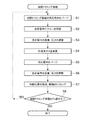
図2は、本発明の実施の形態に係る基板処理方法における成膜トリミング処理を示すフローチャートである。 FIG. 2 is a flowchart showing the film-forming trimming process in the substrate processing method according to the embodiment of the present invention.
図2において、成膜トリミング処理を実行する際、まず、図1の成膜トリミング装置10の反応管12内に、図示省略した処理ガス供給管からN2ガスを直接導入して反応管12内をパージする(ステップS1)。次いで、複数枚のウエハWを収容したウエハボート16を蓋体15上に載置し、蓋体15を上昇させてウエハWを反応管12内に収容する(ステップS2)。
In FIG. 2, when performing the film trimming process, first, N 2 gas is directly introduced into the
次に、反応管12内を、例えば400℃、6.65×10Pa(500mTorr)に調整し(ステップS3)、この状態で処理ガス供給管からSi含有ガスとして、例えば1価のアミノシランであるSiH3(NHC(CH3)3)ガスを導入してウエハWのフォトレジスト膜の表面に吸着させる(ステップS4)(吸着ステップ)。フォトレジスト膜表面にSi含有ガスを吸着させた後、処理ガス供給管からN2ガスを導入して反応管12内の余剰のSi含有ガス等をパージする(ステップS5)。
Next, the inside of the
次いで、余剰のSi含有ガス等がパージされた反応管12内の温度を、例えば400℃に設定し、N2ガスを供給する等して内部圧力を、例えば6.65×10Pa(500mTorr)に調整する(ステップS6)。その後、酸化ガス供給管18を介して、例えばO2ガスを供給し、プラズマ発生部17の電極19間に、例えば500W〜3000Wの高周波電力を印加して酸素をプラズマ励起して酸素ラジカルを発生させ、発生した酸素ラジカルを反応管12に供給してフォトレジスト膜に付着したSi含有ガスを酸化し、これによってSi含有ガスをSi酸化膜に改質してフォトレジスト膜を補強すると共に線状部分をトリミングする(ステップS7)(酸化ステップ)。
Next, the temperature inside the
このとき、Si含有ガス中のC成分及びH成分は、例えばCO2又はH2Oとして飛散し、Siは、例えばSiO2となる。また、マスク膜の開口パターンを形成する線状部分のC成分がCO2として飛散する。これにより、フォトレジスト膜の線状部分の表面をSi酸化膜に改質すると共に、当該線状部分をトリミングする。その後、酸素含有ガスの導入を停止し、処理ガス供給管からN2ガスを導入して反応管12内をパージして成膜トリミング処理の1サイクルを終了する。
At this time, the C component and the H component in the Si-containing gas are scattered as, for example, CO 2 or H 2 O, and Si becomes, for example, SiO 2 . Further, the C component of the linear portion forming the opening pattern of the mask film is scattered as CO 2 . As a result, the surface of the linear portion of the photoresist film is modified to an Si oxide film, and the linear portion is trimmed. Thereafter, the introduction of the oxygen-containing gas is stopped, N 2 gas is introduced from the processing gas supply pipe, the inside of the
次いで、成膜トリミング処理を再度繰り返すか否かの判定を行い(ステップS8)、成膜トリミング処理が完了するまで、ステップS1〜ステップS7を繰り返し、成膜トリミング処理が完了した時点で本処理を終了する。 Next, it is determined whether or not the film trimming process is repeated again (step S8). Steps S1 to S7 are repeated until the film trimming process is completed, and this process is performed when the film trimming process is completed. finish.
図2の処理によれば、ウエハWのフォトレジスト膜表面にSi含有ガスを吸着させ(吸着ステップ)、吸着したSi含有ガスを、酸素をプラズマ励起した酸素ラジカルによって酸化させてSi酸化膜に改質する。また、改質の際、線状部分のC成分が飛散して線状部分がトリミングされる(酸化ステップ)。従って、処理開始時、例えば30nmであったフォトレジスト膜(マスク層)の開口パターンを形成する線状部分の線幅を、例えば7nm程度まで縮小することができる。また、このとき線状部分の両側をSi酸化膜によって補強することができるので、トリミングされた線状部分のパターン倒れを起こすこともない。 2, the Si-containing gas is adsorbed on the surface of the photoresist film of the wafer W (adsorption step), and the adsorbed Si-containing gas is oxidized by oxygen radicals obtained by plasma-excited oxygen to be converted into a Si oxide film. Quality. Further, during the modification, the C component of the linear portion is scattered and the linear portion is trimmed (oxidation step). Therefore, the line width of the linear portion forming the opening pattern of the photoresist film (mask layer) which has been 30 nm, for example, at the start of the processing can be reduced to, for example, about 7 nm. At this time, both sides of the linear portion can be reinforced by the Si oxide film, so that the pattern collapse of the trimmed linear portion does not occur.
また、図2の処理によれば、Si酸化膜の形成と、フォトレジスト膜の線状部分のトリミングを同時に行うことができるので、フォトレジスト膜の線状部分をトリミングした後、線状部分を挟持するようにサイドウォールを形成する従来技術に比べて、処理工程数を減少させることができる。また、従来技術のように、フォトレジストの線状部分をトリミングした後、サイドウォールを形成するために、ウエハを別の基板処理装置に移動させる必要がないので、ディフェクト(欠陥)の発生頻度を低減することもできる。 Further, according to the process of FIG. 2, since the formation of the Si oxide film and the trimming of the linear portion of the photoresist film can be performed at the same time, the linear portion is trimmed after the linear portion of the photoresist film is trimmed. The number of processing steps can be reduced as compared with the conventional technique in which the sidewall is formed so as to be sandwiched. Further, unlike the prior art, it is not necessary to move the wafer to another substrate processing apparatus in order to form the sidewall after trimming the linear portion of the photoresist, so the frequency of occurrence of defects (defects) is reduced. It can also be reduced.
本実施の形態において、成膜トリミング処理が施されるフォトレジスト膜は、開口パターンを形成する線状部分の線幅が、例えば60nm以下の有機膜である。線幅が100nmを超えると、トリミング量が大きすぎて実用的でなくなる。 In the present embodiment, the photoresist film that is subjected to the film-forming trimming process is an organic film having a line width of a linear portion that forms an opening pattern of, for example, 60 nm or less. If the line width exceeds 100 nm, the trimming amount is too large to be practical.
図2の成膜トリミング処理は、吸着ステップによってフォトレジスト膜にSi含有ガスを吸着させた後、酸化ステップによってSi含有ガスをSi酸化膜に改質するものであるが、Si含有ガスをSi酸化膜に改質する際、Si酸化膜が次第に厚くなるに伴って開口パターンを形成する線状部分の線幅が次第にスリム化する。このような成膜トリミング処理は、吸着ステップにおいて、Si含有ガスがフォトレジスト膜表面に均一に吸着するので、これが酸化されたSi酸化膜は、均質且つ均等厚さの補強膜となる。 In the film trimming process of FIG. 2, after the Si-containing gas is adsorbed to the photoresist film by the adsorption step, the Si-containing gas is reformed to the Si oxide film by the oxidation step. When the film is reformed, the line width of the linear portion that forms the opening pattern gradually becomes thinner as the Si oxide film becomes thicker. In such a film trimming process, since the Si-containing gas is uniformly adsorbed on the surface of the photoresist film in the adsorption step, the oxidized Si oxide film becomes a reinforcing film having a uniform and uniform thickness.
図2の処理において、ステップS1〜ステップS7までの処理サイクルは、通常、数十〜数百回繰り返される。成膜トリミング処理の終了時点は、例えば経験上、上記の処理サイクルを何回繰り返せば目的のマスク層が得られるかを参考にサイクル数を決定し、そのサイクル数が終了した時点で成膜トリミング処理が終了したものとみなすようにしてもよい。この場合、フォトレジスト膜の線状部分の線幅は、繰り返しのサイクル数、反応管内の温度、圧力、酸素ラジカル発生時の電力等によって変動する。 In the process of FIG. 2, the processing cycle from step S1 to step S7 is normally repeated several tens to several hundreds of times. The end point of the film trimming process is determined, for example, based on experience, how many times the above processing cycle is repeated to obtain the target mask layer, and the film trimming is performed when the cycle number ends. You may make it consider that the process was complete | finished. In this case, the line width of the linear portion of the photoresist film varies depending on the number of repeated cycles, the temperature and pressure in the reaction tube, the electric power when oxygen radicals are generated, and the like.
図2の処理において、吸着ステップにおける反応管の内部温度は、20℃〜700℃であることが好ましい。反応管の内部温度が20℃よりも低いと吸着ステップにおけるSi含有ガスのフォトレジスト膜への付着が不十分になる虞があり、700℃を越えると酸化ステップ後のSi酸化膜の膜質又は膜厚が不均一になる虞がある。吸着ステップにおける反応管の内部温度が、20℃〜700℃であれば、Si含有ガスのフォトレジスト膜への吸着状態が良好で、均質のSi酸化膜を均等厚で形成することができる。 In the process of FIG. 2, the internal temperature of the reaction tube in the adsorption step is preferably 20 ° C. to 700 ° C. If the internal temperature of the reaction tube is lower than 20 ° C., the Si-containing gas may not be sufficiently adhered to the photoresist film in the adsorption step, and if it exceeds 700 ° C., the quality or film quality of the Si oxide film after the oxidation step The thickness may be non-uniform. If the internal temperature of the reaction tube in the adsorption step is 20 ° C. to 700 ° C., the adsorption state of the Si-containing gas to the photoresist film is good, and a uniform Si oxide film can be formed with a uniform thickness.
図2の処理において、吸着ステップにおける反応管12の内部圧力は、1.33×10⁻¹Pa(1mTorr)〜1.33×10kPa(100Torr)であることが好ましい。これによって、フォトレジスト膜へのSi含有ガスの吸着状態が良好となる。
In the process of FIG. 2, the internal pressure of the
図2の処理において、酸化ステップにおける酸素含有ガスの供給量は、適用される酸素含有ガス中の酸素濃度、プラズマ励起状態等によって異なるが、フォトレジスト膜に付着したSi含有ガスを十分にSi酸化膜に改質することができ、且つ線状部分の線幅を所定の値、例えば7nm程度までトリミングできる量であることが好ましい。 In the process of FIG. 2, the supply amount of the oxygen-containing gas in the oxidation step varies depending on the oxygen concentration in the applied oxygen-containing gas, the plasma excitation state, etc., but the Si-containing gas adhering to the photoresist film is sufficiently oxidized. It is preferable that the amount can be modified into a film and the line width of the linear portion can be trimmed to a predetermined value, for example, about 7 nm.
図2の処理において、酸化ステップにおけるプラズマ発生部17の高周波電源の出力は、例えば500W〜3000Wであることが好ましく、プラズマ発生部17の圧力は、例えば0.133Pa(1mTorr)〜1.33×10²Pa(1000mTorr)であることが好ましい。これによって、プラズマが良好に発生し、且つ反応管12内に十分な酸素ラジカルを供給することができる。
In the process of FIG. 2, the output of the high frequency power source of the
図2の処理において、酸化ステップにおける反応管12の内部圧力は、1.33×10⁻¹Pa(1mTorr)〜1.33×10kPa(100Torr)であることが好ましい。この範囲の圧力にすることにより、フォトレジスト膜表面に吸着したSi含有ガスを良好にSi酸化膜に改質すると共に、線状部分を良好にトリミングすることができる。
In the process of FIG. 2, the internal pressure of the
図2の処理において、酸化ステップにおける処理温度は、20℃〜700℃であることが好ましい。この温度範囲であれば、フォトレジスト膜表面に吸着したSi含有ガスを良好にSi酸化膜に改質することができ、また調整も容易である。 In the treatment of FIG. 2, the treatment temperature in the oxidation step is preferably 20 ° C. to 700 ° C. Within this temperature range, the Si-containing gas adsorbed on the surface of the photoresist film can be satisfactorily modified into a Si oxide film, and adjustment is easy.
図2の処理において、Si含有ガスとして1価のアミノシランを適用したが、2価又は3価のアミノシランを適用することもできる。2価のアミノシランとしては、例えばBTBAS:SiH2(NHC(CH3)3)2、3価のアミノシランとしては、例えば3DMAS:SiH(N(CH3)2)3が挙げられる。 In the process of FIG. 2, monovalent aminosilane is applied as the Si-containing gas, but divalent or trivalent aminosilane can also be applied. An example of the divalent aminosilane is BTBAS: SiH 2 (NHC (CH 3 ) 3 ) 2 , and an example of the trivalent aminosilane is 3DMAS: SiH (N (CH 3 ) 2 ) 3 .
図2の処理において、成膜トリミング処理後のウエハWに対し、例えば、補強膜としてのSi酸化膜の一部をエッチングしてトリミングされた線状部分を露出させる補強膜エッチングステップを有することが好ましい。補強膜エッチングステップを施した後、露出した線状部分をエッチングして消失させることによって、ダブルパターニングと同様の効果が得られる幅が微細化された開口パターンを有する、補強膜としてのSi酸化膜からなるマスク層を得ることができる。 In the process of FIG. 2, for example, the wafer W after the film-trimming process may include a reinforcing film etching step for exposing a trimmed linear portion by etching a part of a Si oxide film as a reinforcing film. preferable. After performing the reinforcing film etching step, the exposed linear portion is etched away so that an effect similar to that of double patterning can be obtained. A mask layer made of can be obtained.
図3は、図2の成膜トリミング処理の具体例を示す工程図である。図3(A)において、このウエハWは、シリコン基材50の表面に形成された処理対象層としてのポリシリコン膜51と、ポリシリコン膜51上に形成されたフォトレジスト膜(マスク層)53とを有する。フォトレジスト膜53には、所定の開口部54が設けられている。
FIG. 3 is a process diagram showing a specific example of the film-forming trimming process of FIG. In FIG. 3A, this wafer W includes a
そして、処理開始前、線状部分の線幅aが30nmであったフォトレジスト膜53に対して成膜トリミング処理を施すと、図3(B)に示したように、線状部分の線幅aが10nm以下までトリミングされると共に、フォトレジスト膜53の線状部分がSi酸化膜55によって補強される。その後、ウエハWをエッチング処理装置に移して、まず、CF4ガスを含む処理ガスのプラズマを用いてSi酸化膜55の一部を除去してフォトレジスト膜53を露出させ、さらに、O2ガスを含む処理ガスのプラズマを用いて該露出したフォトレジスト膜53を除去する。これにより、図3(C)に示すように、2つのSi酸化膜55が対をなす、幅が微細化された開口パターンを有するマスク層を得ることができる(ダブルパターニング)。その後、該マスク層を用いてポリシリコン膜51をエッチングすることにより、該ポリシリコン膜51に半導体デバイスの小型化要求を満たす小さい寸法の開口部を形成することができる。
Then, when the film-trimming process is performed on the
また、本実施の形態において、成膜トリミング処理後の線状部分の両側に形成された補強膜55を、近年の半導体製造技術であるサイドウォール方法におけるサイドウォールとして利用することもできる。このとき、サイドウォール相互間の間隔は、線状部分の線幅のトリミングの程度を制御することによって、換言すれば、成膜するSi酸化膜の膜厚を制御することによって調整することができる。
In the present embodiment, the reinforcing
本実施の形態において、有機膜がフォトレジスト膜である場合について説明したが、成膜トリミング処理される有機膜は、フォトレジスト膜に限定されるものではなく、マスク層として機能する他の有機膜であってもよい。また、有機膜は、被処理基板の表層に限らず、中間層であってもよい。 In this embodiment, the case where the organic film is a photoresist film has been described. However, the organic film to be subjected to the film-trimming process is not limited to the photoresist film, but other organic films that function as a mask layer. It may be. Further, the organic film is not limited to the surface layer of the substrate to be processed, but may be an intermediate layer.
上述した実施の形態において、プラズマ処理が施される基板は半導体デバイス用のウエハに限られず、LCD(Liquid Crystal Display)を含むFPD(Flat Panel Display)等に用いる各種基板や、フォトマスク、CD基板、プリント基板等であってもよい。 In the above-described embodiment, the substrate on which the plasma treatment is performed is not limited to a wafer for semiconductor devices, but various substrates used for FPD (Flat Panel Display) including LCD (Liquid Crystal Display), photomasks, and CD substrates. Or a printed circuit board.
また、本発明の目的は、上述した実施の形態の機能を実現するソフトウェアのプログラムコードを記憶した記憶媒体を、システム或いは装置に供給し、そのシステム或いは装置のコンピュータ(またはCPUやMPU等)が記憶媒体に格納されたプログラムコードを読み出し実行することによっても達成される。 Another object of the present invention is to supply a storage medium storing software program codes for realizing the functions of the above-described embodiments to a system or apparatus, and a computer (or CPU, MPU, etc.) of the system or apparatus. It is also achieved by reading and executing the program code stored in the storage medium.
この場合、記憶媒体から読み出されたプログラムコード自体が上述した実施の形態の機能を実現することになり、そのプログラムコード及び該プログラムコードを記憶した記憶媒体は本発明を構成することになる。 In this case, the program code itself read from the storage medium realizes the functions of the above-described embodiment, and the program code and the storage medium storing the program code constitute the present invention.
また、プログラムコードを供給するための記憶媒体としては、例えば、フロッピー(登録商標)ディスク、ハードディスク、光磁気ディスク、CD−ROM、CD−R、CD−RW、DVD−ROM、DVD−RAM、DVD−RW、DVD+RW等の光ディスク、磁気テープ、不揮発性のメモリカード、ROM等を用いることができる。または、プログラムコードをネットワークを介してダウンロードしてもよい。 Examples of the storage medium for supplying the program code include a floppy (registered trademark) disk, a hard disk, a magneto-optical disk, a CD-ROM, a CD-R, a CD-RW, a DVD-ROM, a DVD-RAM, and a DVD. An optical disc such as RW or DVD + RW, a magnetic tape, a nonvolatile memory card, a ROM, or the like can be used. Alternatively, the program code may be downloaded via a network.
また、コンピュータが読み出したプログラムコードを実行することにより、上述した各実施の形態の機能が実現されるだけではなく、そのプログラムコードの指示に基づき、コンピュータ上で稼動しているOS(オペレーティングシステム)等が実際の処理の一部または全部を行い、その処理によって上述した各実施の形態の機能が実現される場合も含まれる。 Further, by executing the program code read by the computer, not only the functions of the above-described embodiments are realized, but also an OS (Operating System) running on the computer based on the instruction of the program code. Includes a case where the functions of the above-described embodiments are realized by performing part or all of the actual processing.
さらに、記憶媒体から読み出されたプログラムコードが、コンピュータに挿入された機能拡張ボードやコンピュータに接続された機能拡張ユニットに備わるメモリに書き込まれた後、そのプログラムコードの指示に基づき、その拡張機能を拡張ボードや拡張ユニットに備わるCPU等が実際の処理の一部または全部を行い、その処理によって上述した各実施の形態の機能が実現される場合も含まれる。 Furthermore, after the program code read from the storage medium is written to a memory provided in a function expansion board inserted into the computer or a function expansion unit connected to the computer, the expanded function is based on the instruction of the program code. This includes a case where a CPU or the like provided on the expansion board or the expansion unit performs part or all of the actual processing and the functions of the above-described embodiments are realized by the processing.
10 基板処理装置(成膜トリミング装置)
12 反応管
17 プラズマ発生部
18 酸化ガス供給管
50 シリコン基材
51 アモルファスカーボン膜
53 フォトレジスト膜
54 開口部
55 Si酸化膜
10 Substrate processing equipment (film trimming equipment)
12
Claims (9)
該成膜トリミングステップは、前記有機膜表面にSi含有ガスを吸着させる吸着ステップと、吸着したSi含有ガスをSi酸化膜に改質すると共に前記有機膜の前記線幅を微細化する酸化ステップを有することを特徴とする基板処理方法。 A processing target layer, a substrate processing method for processing a substrate having an organic film, the line width of the linear portions that form a opening pattern of the organic film while forming the reinforcement film on the organic film surface fine have a film-forming trimming step of reduction,
The film trimming step includes an adsorption step for adsorbing a Si-containing gas on the surface of the organic film, and an oxidation step for modifying the adsorbed Si-containing gas into a Si oxide film and reducing the line width of the organic film. the substrate processing method, characterized by chromatic.
Of claims 1 to 8, characterized in that it has a reinforcing film etching step to expose the trimmed the linear portion of the partially etched to the organic layer of the reinforcing film formed by the film forming trimming step The substrate processing method of any one of Claims 1.
Priority Applications (2)
| Application Number | Priority Date | Filing Date | Title |
|---|---|---|---|
| JP2009061139A JP5275094B2 (en) | 2009-03-13 | 2009-03-13 | Substrate processing method |
| US12/720,197 US8202805B2 (en) | 2009-03-13 | 2010-03-09 | Substrate processing method |
Applications Claiming Priority (1)
| Application Number | Priority Date | Filing Date | Title |
|---|---|---|---|
| JP2009061139A JP5275094B2 (en) | 2009-03-13 | 2009-03-13 | Substrate processing method |
Publications (3)
| Publication Number | Publication Date |
|---|---|
| JP2010219106A JP2010219106A (en) | 2010-09-30 |
| JP2010219106A5 JP2010219106A5 (en) | 2012-04-26 |
| JP5275094B2 true JP5275094B2 (en) | 2013-08-28 |
Family
ID=42731082
Family Applications (1)
| Application Number | Title | Priority Date | Filing Date |
|---|---|---|---|
| JP2009061139A Active JP5275094B2 (en) | 2009-03-13 | 2009-03-13 | Substrate processing method |
Country Status (2)
| Country | Link |
|---|---|
| US (1) | US8202805B2 (en) |
| JP (1) | JP5275094B2 (en) |
Families Citing this family (293)
| Publication number | Priority date | Publication date | Assignee | Title |
|---|---|---|---|---|
| US10378106B2 (en) | 2008-11-14 | 2019-08-13 | Asm Ip Holding B.V. | Method of forming insulation film by modified PEALD |
| US9394608B2 (en) | 2009-04-06 | 2016-07-19 | Asm America, Inc. | Semiconductor processing reactor and components thereof |
| US8802201B2 (en) | 2009-08-14 | 2014-08-12 | Asm America, Inc. | Systems and methods for thin-film deposition of metal oxides using excited nitrogen-oxygen species |
| US8252691B2 (en) * | 2010-04-14 | 2012-08-28 | Asm Genitech Korea Ltd. | Method of forming semiconductor patterns |
| JP5588856B2 (en) * | 2010-12-27 | 2014-09-10 | 東京エレクトロン株式会社 | Method and apparatus for forming oxide film on carbon film |
| US8771807B2 (en) * | 2011-05-24 | 2014-07-08 | Air Products And Chemicals, Inc. | Organoaminosilane precursors and methods for making and using same |
| US9312155B2 (en) | 2011-06-06 | 2016-04-12 | Asm Japan K.K. | High-throughput semiconductor-processing apparatus equipped with multiple dual-chamber modules |
| US10364496B2 (en) | 2011-06-27 | 2019-07-30 | Asm Ip Holding B.V. | Dual section module having shared and unshared mass flow controllers |
| US10854498B2 (en) | 2011-07-15 | 2020-12-01 | Asm Ip Holding B.V. | Wafer-supporting device and method for producing same |
| US20130023129A1 (en) | 2011-07-20 | 2013-01-24 | Asm America, Inc. | Pressure transmitter for a semiconductor processing environment |
| US9017481B1 (en) | 2011-10-28 | 2015-04-28 | Asm America, Inc. | Process feed management for semiconductor substrate processing |
| CN104011834B (en) * | 2011-12-29 | 2016-08-24 | 英特尔公司 | The pitch divisions photoetching process of interval body auxiliary |
| US9659799B2 (en) | 2012-08-28 | 2017-05-23 | Asm Ip Holding B.V. | Systems and methods for dynamic semiconductor process scheduling |
| US10714315B2 (en) | 2012-10-12 | 2020-07-14 | Asm Ip Holdings B.V. | Semiconductor reaction chamber showerhead |
| US20160376700A1 (en) | 2013-02-01 | 2016-12-29 | Asm Ip Holding B.V. | System for treatment of deposition reactor |
| US9589770B2 (en) | 2013-03-08 | 2017-03-07 | Asm Ip Holding B.V. | Method and systems for in-situ formation of intermediate reactive species |
| US9484191B2 (en) | 2013-03-08 | 2016-11-01 | Asm Ip Holding B.V. | Pulsed remote plasma method and system |
| US9240412B2 (en) | 2013-09-27 | 2016-01-19 | Asm Ip Holding B.V. | Semiconductor structure and device and methods of forming same using selective epitaxial process |
| US10683571B2 (en) | 2014-02-25 | 2020-06-16 | Asm Ip Holding B.V. | Gas supply manifold and method of supplying gases to chamber using same |
| US10167557B2 (en) | 2014-03-18 | 2019-01-01 | Asm Ip Holding B.V. | Gas distribution system, reactor including the system, and methods of using the same |
| US11015245B2 (en) | 2014-03-19 | 2021-05-25 | Asm Ip Holding B.V. | Gas-phase reactor and system having exhaust plenum and components thereof |
| US10858737B2 (en) | 2014-07-28 | 2020-12-08 | Asm Ip Holding B.V. | Showerhead assembly and components thereof |
| US9890456B2 (en) | 2014-08-21 | 2018-02-13 | Asm Ip Holding B.V. | Method and system for in situ formation of gas-phase compounds |
| US9657845B2 (en) | 2014-10-07 | 2017-05-23 | Asm Ip Holding B.V. | Variable conductance gas distribution apparatus and method |
| US10941490B2 (en) | 2014-10-07 | 2021-03-09 | Asm Ip Holding B.V. | Multiple temperature range susceptor, assembly, reactor and system including the susceptor, and methods of using the same |
| KR102263121B1 (en) | 2014-12-22 | 2021-06-09 | 에이에스엠 아이피 홀딩 비.브이. | Semiconductor device and manufacuring method thereof |
| US10529542B2 (en) | 2015-03-11 | 2020-01-07 | Asm Ip Holdings B.V. | Cross-flow reactor and method |
| US10276355B2 (en) | 2015-03-12 | 2019-04-30 | Asm Ip Holding B.V. | Multi-zone reactor, system including the reactor, and method of using the same |
| US10458018B2 (en) | 2015-06-26 | 2019-10-29 | Asm Ip Holding B.V. | Structures including metal carbide material, devices including the structures, and methods of forming same |
| US10600673B2 (en) | 2015-07-07 | 2020-03-24 | Asm Ip Holding B.V. | Magnetic susceptor to baseplate seal |
| US9960072B2 (en) | 2015-09-29 | 2018-05-01 | Asm Ip Holding B.V. | Variable adjustment for precise matching of multiple chamber cavity housings |
| US10211308B2 (en) | 2015-10-21 | 2019-02-19 | Asm Ip Holding B.V. | NbMC layers |
| US10322384B2 (en) | 2015-11-09 | 2019-06-18 | Asm Ip Holding B.V. | Counter flow mixer for process chamber |
| US11139308B2 (en) | 2015-12-29 | 2021-10-05 | Asm Ip Holding B.V. | Atomic layer deposition of III-V compounds to form V-NAND devices |
| US10529554B2 (en) | 2016-02-19 | 2020-01-07 | Asm Ip Holding B.V. | Method for forming silicon nitride film selectively on sidewalls or flat surfaces of trenches |
| US10468251B2 (en) | 2016-02-19 | 2019-11-05 | Asm Ip Holding B.V. | Method for forming spacers using silicon nitride film for spacer-defined multiple patterning |
| US10501866B2 (en) | 2016-03-09 | 2019-12-10 | Asm Ip Holding B.V. | Gas distribution apparatus for improved film uniformity in an epitaxial system |
| US10343920B2 (en) | 2016-03-18 | 2019-07-09 | Asm Ip Holding B.V. | Aligned carbon nanotubes |
| US9892913B2 (en) | 2016-03-24 | 2018-02-13 | Asm Ip Holding B.V. | Radial and thickness control via biased multi-port injection settings |
| US10190213B2 (en) | 2016-04-21 | 2019-01-29 | Asm Ip Holding B.V. | Deposition of metal borides |
| US10865475B2 (en) | 2016-04-21 | 2020-12-15 | Asm Ip Holding B.V. | Deposition of metal borides and silicides |
| US10032628B2 (en) | 2016-05-02 | 2018-07-24 | Asm Ip Holding B.V. | Source/drain performance through conformal solid state doping |
| US10367080B2 (en) | 2016-05-02 | 2019-07-30 | Asm Ip Holding B.V. | Method of forming a germanium oxynitride film |
| KR102592471B1 (en) | 2016-05-17 | 2023-10-20 | 에이에스엠 아이피 홀딩 비.브이. | Method of forming metal interconnection and method of fabricating semiconductor device using the same |
| US11453943B2 (en) | 2016-05-25 | 2022-09-27 | Asm Ip Holding B.V. | Method for forming carbon-containing silicon/metal oxide or nitride film by ALD using silicon precursor and hydrocarbon precursor |
| US10388509B2 (en) | 2016-06-28 | 2019-08-20 | Asm Ip Holding B.V. | Formation of epitaxial layers via dislocation filtering |
| US9859151B1 (en) | 2016-07-08 | 2018-01-02 | Asm Ip Holding B.V. | Selective film deposition method to form air gaps |
| US10612137B2 (en) | 2016-07-08 | 2020-04-07 | Asm Ip Holdings B.V. | Organic reactants for atomic layer deposition |
| US10714385B2 (en) | 2016-07-19 | 2020-07-14 | Asm Ip Holding B.V. | Selective deposition of tungsten |
| US10381226B2 (en) | 2016-07-27 | 2019-08-13 | Asm Ip Holding B.V. | Method of processing substrate |
| US9812320B1 (en) | 2016-07-28 | 2017-11-07 | Asm Ip Holding B.V. | Method and apparatus for filling a gap |
| KR102532607B1 (en) | 2016-07-28 | 2023-05-15 | 에이에스엠 아이피 홀딩 비.브이. | Substrate processing apparatus and method of operating the same |
| US9887082B1 (en) | 2016-07-28 | 2018-02-06 | Asm Ip Holding B.V. | Method and apparatus for filling a gap |
| US10395919B2 (en) | 2016-07-28 | 2019-08-27 | Asm Ip Holding B.V. | Method and apparatus for filling a gap |
| KR102613349B1 (en) | 2016-08-25 | 2023-12-14 | 에이에스엠 아이피 홀딩 비.브이. | Exhaust apparatus and substrate processing apparatus and thin film fabricating method using the same |
| US10410943B2 (en) | 2016-10-13 | 2019-09-10 | Asm Ip Holding B.V. | Method for passivating a surface of a semiconductor and related systems |
| US10643826B2 (en) | 2016-10-26 | 2020-05-05 | Asm Ip Holdings B.V. | Methods for thermally calibrating reaction chambers |
| US11532757B2 (en) | 2016-10-27 | 2022-12-20 | Asm Ip Holding B.V. | Deposition of charge trapping layers |
| US10435790B2 (en) | 2016-11-01 | 2019-10-08 | Asm Ip Holding B.V. | Method of subatmospheric plasma-enhanced ALD using capacitively coupled electrodes with narrow gap |
| US10229833B2 (en) | 2016-11-01 | 2019-03-12 | Asm Ip Holding B.V. | Methods for forming a transition metal nitride film on a substrate by atomic layer deposition and related semiconductor device structures |
| US10714350B2 (en) | 2016-11-01 | 2020-07-14 | ASM IP Holdings, B.V. | Methods for forming a transition metal niobium nitride film on a substrate by atomic layer deposition and related semiconductor device structures |
| US10643904B2 (en) | 2016-11-01 | 2020-05-05 | Asm Ip Holdings B.V. | Methods for forming a semiconductor device and related semiconductor device structures |
| US10134757B2 (en) | 2016-11-07 | 2018-11-20 | Asm Ip Holding B.V. | Method of processing a substrate and a device manufactured by using the method |
| KR102546317B1 (en) | 2016-11-15 | 2023-06-21 | 에이에스엠 아이피 홀딩 비.브이. | Gas supply unit and substrate processing apparatus including the same |
| US10340135B2 (en) | 2016-11-28 | 2019-07-02 | Asm Ip Holding B.V. | Method of topologically restricted plasma-enhanced cyclic deposition of silicon or metal nitride |
| KR20180068582A (en) | 2016-12-14 | 2018-06-22 | 에이에스엠 아이피 홀딩 비.브이. | Substrate processing apparatus |
| US11447861B2 (en) | 2016-12-15 | 2022-09-20 | Asm Ip Holding B.V. | Sequential infiltration synthesis apparatus and a method of forming a patterned structure |
| US11581186B2 (en) | 2016-12-15 | 2023-02-14 | Asm Ip Holding B.V. | Sequential infiltration synthesis apparatus |
| US10566212B2 (en) | 2016-12-19 | 2020-02-18 | Lam Research Corporation | Designer atomic layer etching |
| KR20180070971A (en) | 2016-12-19 | 2018-06-27 | 에이에스엠 아이피 홀딩 비.브이. | Substrate processing apparatus |
| US10269558B2 (en) | 2016-12-22 | 2019-04-23 | Asm Ip Holding B.V. | Method of forming a structure on a substrate |
| US10867788B2 (en) | 2016-12-28 | 2020-12-15 | Asm Ip Holding B.V. | Method of forming a structure on a substrate |
| US10655221B2 (en) | 2017-02-09 | 2020-05-19 | Asm Ip Holding B.V. | Method for depositing oxide film by thermal ALD and PEALD |
| US10468261B2 (en) | 2017-02-15 | 2019-11-05 | Asm Ip Holding B.V. | Methods for forming a metallic film on a substrate by cyclical deposition and related semiconductor device structures |
| US10283353B2 (en) | 2017-03-29 | 2019-05-07 | Asm Ip Holding B.V. | Method of reforming insulating film deposited on substrate with recess pattern |
| US10529563B2 (en) | 2017-03-29 | 2020-01-07 | Asm Ip Holdings B.V. | Method for forming doped metal oxide films on a substrate by cyclical deposition and related semiconductor device structures |
| US10832909B2 (en) | 2017-04-24 | 2020-11-10 | Lam Research Corporation | Atomic layer etch, reactive precursors and energetic sources for patterning applications |
| KR102457289B1 (en) | 2017-04-25 | 2022-10-21 | 에이에스엠 아이피 홀딩 비.브이. | Method for depositing a thin film and manufacturing a semiconductor device |
| US10446393B2 (en) | 2017-05-08 | 2019-10-15 | Asm Ip Holding B.V. | Methods for forming silicon-containing epitaxial layers and related semiconductor device structures |
| US10892156B2 (en) | 2017-05-08 | 2021-01-12 | Asm Ip Holding B.V. | Methods for forming a silicon nitride film on a substrate and related semiconductor device structures |
| US10770286B2 (en) | 2017-05-08 | 2020-09-08 | Asm Ip Holdings B.V. | Methods for selectively forming a silicon nitride film on a substrate and related semiconductor device structures |
| US10504742B2 (en) | 2017-05-31 | 2019-12-10 | Asm Ip Holding B.V. | Method of atomic layer etching using hydrogen plasma |
| US10886123B2 (en) | 2017-06-02 | 2021-01-05 | Asm Ip Holding B.V. | Methods for forming low temperature semiconductor layers and related semiconductor device structures |
| US11306395B2 (en) | 2017-06-28 | 2022-04-19 | Asm Ip Holding B.V. | Methods for depositing a transition metal nitride film on a substrate by atomic layer deposition and related deposition apparatus |
| US10685834B2 (en) | 2017-07-05 | 2020-06-16 | Asm Ip Holdings B.V. | Methods for forming a silicon germanium tin layer and related semiconductor device structures |
| KR20190009245A (en) | 2017-07-18 | 2019-01-28 | 에이에스엠 아이피 홀딩 비.브이. | Methods for forming a semiconductor device structure and related semiconductor device structures |
| US11018002B2 (en) | 2017-07-19 | 2021-05-25 | Asm Ip Holding B.V. | Method for selectively depositing a Group IV semiconductor and related semiconductor device structures |
| US11374112B2 (en) | 2017-07-19 | 2022-06-28 | Asm Ip Holding B.V. | Method for depositing a group IV semiconductor and related semiconductor device structures |
| US10541333B2 (en) | 2017-07-19 | 2020-01-21 | Asm Ip Holding B.V. | Method for depositing a group IV semiconductor and related semiconductor device structures |
| US10590535B2 (en) | 2017-07-26 | 2020-03-17 | Asm Ip Holdings B.V. | Chemical treatment, deposition and/or infiltration apparatus and method for using the same |
| US10312055B2 (en) | 2017-07-26 | 2019-06-04 | Asm Ip Holding B.V. | Method of depositing film by PEALD using negative bias |
| US10605530B2 (en) | 2017-07-26 | 2020-03-31 | Asm Ip Holding B.V. | Assembly of a liner and a flange for a vertical furnace as well as the liner and the vertical furnace |
| US10770336B2 (en) | 2017-08-08 | 2020-09-08 | Asm Ip Holding B.V. | Substrate lift mechanism and reactor including same |
| US10692741B2 (en) | 2017-08-08 | 2020-06-23 | Asm Ip Holdings B.V. | Radiation shield |
| US11769682B2 (en) | 2017-08-09 | 2023-09-26 | Asm Ip Holding B.V. | Storage apparatus for storing cassettes for substrates and processing apparatus equipped therewith |
| US10249524B2 (en) | 2017-08-09 | 2019-04-02 | Asm Ip Holding B.V. | Cassette holder assembly for a substrate cassette and holding member for use in such assembly |
| US11139191B2 (en) | 2017-08-09 | 2021-10-05 | Asm Ip Holding B.V. | Storage apparatus for storing cassettes for substrates and processing apparatus equipped therewith |
| USD900036S1 (en) | 2017-08-24 | 2020-10-27 | Asm Ip Holding B.V. | Heater electrical connector and adapter |
| US11830730B2 (en) | 2017-08-29 | 2023-11-28 | Asm Ip Holding B.V. | Layer forming method and apparatus |
| US11295980B2 (en) | 2017-08-30 | 2022-04-05 | Asm Ip Holding B.V. | Methods for depositing a molybdenum metal film over a dielectric surface of a substrate by a cyclical deposition process and related semiconductor device structures |
| KR102491945B1 (en) | 2017-08-30 | 2023-01-26 | 에이에스엠 아이피 홀딩 비.브이. | Substrate processing apparatus |
| US11056344B2 (en) | 2017-08-30 | 2021-07-06 | Asm Ip Holding B.V. | Layer forming method |
| US10607895B2 (en) | 2017-09-18 | 2020-03-31 | Asm Ip Holdings B.V. | Method for forming a semiconductor device structure comprising a gate fill metal |
| KR102630301B1 (en) | 2017-09-21 | 2024-01-29 | 에이에스엠 아이피 홀딩 비.브이. | Method of sequential infiltration synthesis treatment of infiltrateable material and structures and devices formed using same |
| US10844484B2 (en) | 2017-09-22 | 2020-11-24 | Asm Ip Holding B.V. | Apparatus for dispensing a vapor phase reactant to a reaction chamber and related methods |
| US10658205B2 (en) | 2017-09-28 | 2020-05-19 | Asm Ip Holdings B.V. | Chemical dispensing apparatus and methods for dispensing a chemical to a reaction chamber |
| US10403504B2 (en) | 2017-10-05 | 2019-09-03 | Asm Ip Holding B.V. | Method for selectively depositing a metallic film on a substrate |
| US10319588B2 (en) | 2017-10-10 | 2019-06-11 | Asm Ip Holding B.V. | Method for depositing a metal chalcogenide on a substrate by cyclical deposition |
| US10923344B2 (en) | 2017-10-30 | 2021-02-16 | Asm Ip Holding B.V. | Methods for forming a semiconductor structure and related semiconductor structures |
| US10910262B2 (en) | 2017-11-16 | 2021-02-02 | Asm Ip Holding B.V. | Method of selectively depositing a capping layer structure on a semiconductor device structure |
| KR102443047B1 (en) | 2017-11-16 | 2022-09-14 | 에이에스엠 아이피 홀딩 비.브이. | Method of processing a substrate and a device manufactured by the same |
| US11022879B2 (en) | 2017-11-24 | 2021-06-01 | Asm Ip Holding B.V. | Method of forming an enhanced unexposed photoresist layer |
| CN111344522B (en) | 2017-11-27 | 2022-04-12 | 阿斯莫Ip控股公司 | Including clean mini-environment device |
| KR102597978B1 (en) | 2017-11-27 | 2023-11-06 | 에이에스엠 아이피 홀딩 비.브이. | Storage device for storing wafer cassettes for use with batch furnaces |
| US10290508B1 (en) | 2017-12-05 | 2019-05-14 | Asm Ip Holding B.V. | Method for forming vertical spacers for spacer-defined patterning |
| US10872771B2 (en) | 2018-01-16 | 2020-12-22 | Asm Ip Holding B. V. | Method for depositing a material film on a substrate within a reaction chamber by a cyclical deposition process and related device structures |
| CN111630203A (en) | 2018-01-19 | 2020-09-04 | Asm Ip私人控股有限公司 | Method for depositing gap filling layer by plasma auxiliary deposition |
| TW202325889A (en) | 2018-01-19 | 2023-07-01 | 荷蘭商Asm 智慧財產控股公司 | Deposition method |
| USD903477S1 (en) | 2018-01-24 | 2020-12-01 | Asm Ip Holdings B.V. | Metal clamp |
| US11018047B2 (en) | 2018-01-25 | 2021-05-25 | Asm Ip Holding B.V. | Hybrid lift pin |
| USD880437S1 (en) | 2018-02-01 | 2020-04-07 | Asm Ip Holding B.V. | Gas supply plate for semiconductor manufacturing apparatus |
| US10535516B2 (en) | 2018-02-01 | 2020-01-14 | Asm Ip Holdings B.V. | Method for depositing a semiconductor structure on a surface of a substrate and related semiconductor structures |
| US11081345B2 (en) | 2018-02-06 | 2021-08-03 | Asm Ip Holding B.V. | Method of post-deposition treatment for silicon oxide film |
| EP3737779A1 (en) | 2018-02-14 | 2020-11-18 | ASM IP Holding B.V. | A method for depositing a ruthenium-containing film on a substrate by a cyclical deposition process |
| US10896820B2 (en) | 2018-02-14 | 2021-01-19 | Asm Ip Holding B.V. | Method for depositing a ruthenium-containing film on a substrate by a cyclical deposition process |
| US10731249B2 (en) | 2018-02-15 | 2020-08-04 | Asm Ip Holding B.V. | Method of forming a transition metal containing film on a substrate by a cyclical deposition process, a method for supplying a transition metal halide compound to a reaction chamber, and related vapor deposition apparatus |
| KR102636427B1 (en) | 2018-02-20 | 2024-02-13 | 에이에스엠 아이피 홀딩 비.브이. | Substrate processing method and apparatus |
| US10658181B2 (en) | 2018-02-20 | 2020-05-19 | Asm Ip Holding B.V. | Method of spacer-defined direct patterning in semiconductor fabrication |
| US10975470B2 (en) | 2018-02-23 | 2021-04-13 | Asm Ip Holding B.V. | Apparatus for detecting or monitoring for a chemical precursor in a high temperature environment |
| US11473195B2 (en) | 2018-03-01 | 2022-10-18 | Asm Ip Holding B.V. | Semiconductor processing apparatus and a method for processing a substrate |
| US11629406B2 (en) | 2018-03-09 | 2023-04-18 | Asm Ip Holding B.V. | Semiconductor processing apparatus comprising one or more pyrometers for measuring a temperature of a substrate during transfer of the substrate |
| US11114283B2 (en) | 2018-03-16 | 2021-09-07 | Asm Ip Holding B.V. | Reactor, system including the reactor, and methods of manufacturing and using same |
| KR102646467B1 (en) | 2018-03-27 | 2024-03-11 | 에이에스엠 아이피 홀딩 비.브이. | Method of forming an electrode on a substrate and a semiconductor device structure including an electrode |
| US11230766B2 (en) | 2018-03-29 | 2022-01-25 | Asm Ip Holding B.V. | Substrate processing apparatus and method |
| US11088002B2 (en) | 2018-03-29 | 2021-08-10 | Asm Ip Holding B.V. | Substrate rack and a substrate processing system and method |
| US10510536B2 (en) | 2018-03-29 | 2019-12-17 | Asm Ip Holding B.V. | Method of depositing a co-doped polysilicon film on a surface of a substrate within a reaction chamber |
| KR102501472B1 (en) | 2018-03-30 | 2023-02-20 | 에이에스엠 아이피 홀딩 비.브이. | Substrate processing method |
| TW202344708A (en) | 2018-05-08 | 2023-11-16 | 荷蘭商Asm Ip私人控股有限公司 | Methods for depositing an oxide film on a substrate by a cyclical deposition process and related device structures |
| TWI816783B (en) | 2018-05-11 | 2023-10-01 | 荷蘭商Asm 智慧財產控股公司 | Methods for forming a doped metal carbide film on a substrate and related semiconductor device structures |
| KR102596988B1 (en) | 2018-05-28 | 2023-10-31 | 에이에스엠 아이피 홀딩 비.브이. | Method of processing a substrate and a device manufactured by the same |
| US11270899B2 (en) | 2018-06-04 | 2022-03-08 | Asm Ip Holding B.V. | Wafer handling chamber with moisture reduction |
| US11718913B2 (en) | 2018-06-04 | 2023-08-08 | Asm Ip Holding B.V. | Gas distribution system and reactor system including same |
| US11286562B2 (en) | 2018-06-08 | 2022-03-29 | Asm Ip Holding B.V. | Gas-phase chemical reactor and method of using same |
| US10797133B2 (en) | 2018-06-21 | 2020-10-06 | Asm Ip Holding B.V. | Method for depositing a phosphorus doped silicon arsenide film and related semiconductor device structures |
| KR102568797B1 (en) | 2018-06-21 | 2023-08-21 | 에이에스엠 아이피 홀딩 비.브이. | Substrate processing system |
| WO2020003000A1 (en) | 2018-06-27 | 2020-01-02 | Asm Ip Holding B.V. | Cyclic deposition methods for forming metal-containing material and films and structures including the metal-containing material |
| US11492703B2 (en) | 2018-06-27 | 2022-11-08 | Asm Ip Holding B.V. | Cyclic deposition methods for forming metal-containing material and films and structures including the metal-containing material |
| KR20200002519A (en) | 2018-06-29 | 2020-01-08 | 에이에스엠 아이피 홀딩 비.브이. | Method for depositing a thin film and manufacturing a semiconductor device |
| US10612136B2 (en) | 2018-06-29 | 2020-04-07 | ASM IP Holding, B.V. | Temperature-controlled flange and reactor system including same |
| US10388513B1 (en) | 2018-07-03 | 2019-08-20 | Asm Ip Holding B.V. | Method for depositing silicon-free carbon-containing film as gap-fill layer by pulse plasma-assisted deposition |
| US10755922B2 (en) | 2018-07-03 | 2020-08-25 | Asm Ip Holding B.V. | Method for depositing silicon-free carbon-containing film as gap-fill layer by pulse plasma-assisted deposition |
| US10767789B2 (en) | 2018-07-16 | 2020-09-08 | Asm Ip Holding B.V. | Diaphragm valves, valve components, and methods for forming valve components |
| US10483099B1 (en) | 2018-07-26 | 2019-11-19 | Asm Ip Holding B.V. | Method for forming thermally stable organosilicon polymer film |
| US11053591B2 (en) | 2018-08-06 | 2021-07-06 | Asm Ip Holding B.V. | Multi-port gas injection system and reactor system including same |
| US10883175B2 (en) | 2018-08-09 | 2021-01-05 | Asm Ip Holding B.V. | Vertical furnace for processing substrates and a liner for use therein |
| US10829852B2 (en) | 2018-08-16 | 2020-11-10 | Asm Ip Holding B.V. | Gas distribution device for a wafer processing apparatus |
| US11430674B2 (en) | 2018-08-22 | 2022-08-30 | Asm Ip Holding B.V. | Sensor array, apparatus for dispensing a vapor phase reactant to a reaction chamber and related methods |
| KR20200030162A (en) | 2018-09-11 | 2020-03-20 | 에이에스엠 아이피 홀딩 비.브이. | Method for deposition of a thin film |
| US11024523B2 (en) | 2018-09-11 | 2021-06-01 | Asm Ip Holding B.V. | Substrate processing apparatus and method |
| US11049751B2 (en) | 2018-09-14 | 2021-06-29 | Asm Ip Holding B.V. | Cassette supply system to store and handle cassettes and processing apparatus equipped therewith |
| CN110970344A (en) | 2018-10-01 | 2020-04-07 | Asm Ip控股有限公司 | Substrate holding apparatus, system including the same, and method of using the same |
| US11232963B2 (en) | 2018-10-03 | 2022-01-25 | Asm Ip Holding B.V. | Substrate processing apparatus and method |
| KR102592699B1 (en) | 2018-10-08 | 2023-10-23 | 에이에스엠 아이피 홀딩 비.브이. | Substrate support unit and apparatuses for depositing thin film and processing the substrate including the same |
| US10847365B2 (en) | 2018-10-11 | 2020-11-24 | Asm Ip Holding B.V. | Method of forming conformal silicon carbide film by cyclic CVD |
| US10811256B2 (en) | 2018-10-16 | 2020-10-20 | Asm Ip Holding B.V. | Method for etching a carbon-containing feature |
| KR102605121B1 (en) | 2018-10-19 | 2023-11-23 | 에이에스엠 아이피 홀딩 비.브이. | Substrate processing apparatus and substrate processing method |
| KR102546322B1 (en) | 2018-10-19 | 2023-06-21 | 에이에스엠 아이피 홀딩 비.브이. | Substrate processing apparatus and substrate processing method |
| USD948463S1 (en) | 2018-10-24 | 2022-04-12 | Asm Ip Holding B.V. | Susceptor for semiconductor substrate supporting apparatus |
| US10381219B1 (en) | 2018-10-25 | 2019-08-13 | Asm Ip Holding B.V. | Methods for forming a silicon nitride film |
| US11087997B2 (en) | 2018-10-31 | 2021-08-10 | Asm Ip Holding B.V. | Substrate processing apparatus for processing substrates |
| KR20200051105A (en) | 2018-11-02 | 2020-05-13 | 에이에스엠 아이피 홀딩 비.브이. | Substrate support unit and substrate processing apparatus including the same |
| US11572620B2 (en) | 2018-11-06 | 2023-02-07 | Asm Ip Holding B.V. | Methods for selectively depositing an amorphous silicon film on a substrate |
| US11031242B2 (en) | 2018-11-07 | 2021-06-08 | Asm Ip Holding B.V. | Methods for depositing a boron doped silicon germanium film |
| US10847366B2 (en) | 2018-11-16 | 2020-11-24 | Asm Ip Holding B.V. | Methods for depositing a transition metal chalcogenide film on a substrate by a cyclical deposition process |
| US10818758B2 (en) | 2018-11-16 | 2020-10-27 | Asm Ip Holding B.V. | Methods for forming a metal silicate film on a substrate in a reaction chamber and related semiconductor device structures |
| US10559458B1 (en) | 2018-11-26 | 2020-02-11 | Asm Ip Holding B.V. | Method of forming oxynitride film |
| US11217444B2 (en) | 2018-11-30 | 2022-01-04 | Asm Ip Holding B.V. | Method for forming an ultraviolet radiation responsive metal oxide-containing film |
| KR102636428B1 (en) | 2018-12-04 | 2024-02-13 | 에이에스엠 아이피 홀딩 비.브이. | A method for cleaning a substrate processing apparatus |
| US11158513B2 (en) | 2018-12-13 | 2021-10-26 | Asm Ip Holding B.V. | Methods for forming a rhenium-containing film on a substrate by a cyclical deposition process and related semiconductor device structures |
| JP2020096183A (en) | 2018-12-14 | 2020-06-18 | エーエスエム・アイピー・ホールディング・ベー・フェー | Method of forming device structure using selective deposition of gallium nitride, and system for the same |
| TWI819180B (en) | 2019-01-17 | 2023-10-21 | 荷蘭商Asm 智慧財產控股公司 | Methods of forming a transition metal containing film on a substrate by a cyclical deposition process |
| KR20200091543A (en) | 2019-01-22 | 2020-07-31 | 에이에스엠 아이피 홀딩 비.브이. | Semiconductor processing device |
| CN111524788B (en) | 2019-02-01 | 2023-11-24 | Asm Ip私人控股有限公司 | Method for topologically selective film formation of silicon oxide |
| KR20200102357A (en) | 2019-02-20 | 2020-08-31 | 에이에스엠 아이피 홀딩 비.브이. | Apparatus and methods for plug fill deposition in 3-d nand applications |
| TW202044325A (en) | 2019-02-20 | 2020-12-01 | 荷蘭商Asm Ip私人控股有限公司 | Method of filling a recess formed within a surface of a substrate, semiconductor structure formed according to the method, and semiconductor processing apparatus |
| TW202104632A (en) | 2019-02-20 | 2021-02-01 | 荷蘭商Asm Ip私人控股有限公司 | Cyclical deposition method and apparatus for filling a recess formed within a substrate surface |
| KR102626263B1 (en) | 2019-02-20 | 2024-01-16 | 에이에스엠 아이피 홀딩 비.브이. | Cyclical deposition method including treatment step and apparatus for same |
| TW202100794A (en) | 2019-02-22 | 2021-01-01 | 荷蘭商Asm Ip私人控股有限公司 | Substrate processing apparatus and method for processing substrate |
| KR20200108243A (en) | 2019-03-08 | 2020-09-17 | 에이에스엠 아이피 홀딩 비.브이. | Structure Including SiOC Layer and Method of Forming Same |
| KR20200108242A (en) | 2019-03-08 | 2020-09-17 | 에이에스엠 아이피 홀딩 비.브이. | Method for Selective Deposition of Silicon Nitride Layer and Structure Including Selectively-Deposited Silicon Nitride Layer |
| KR20200108248A (en) | 2019-03-08 | 2020-09-17 | 에이에스엠 아이피 홀딩 비.브이. | STRUCTURE INCLUDING SiOCN LAYER AND METHOD OF FORMING SAME |
| JP2020167398A (en) | 2019-03-28 | 2020-10-08 | エーエスエム・アイピー・ホールディング・ベー・フェー | Door opener and substrate processing apparatus provided therewith |
| KR20200116855A (en) | 2019-04-01 | 2020-10-13 | 에이에스엠 아이피 홀딩 비.브이. | Method of manufacturing semiconductor device |
| KR20200123380A (en) | 2019-04-19 | 2020-10-29 | 에이에스엠 아이피 홀딩 비.브이. | Layer forming method and apparatus |
| KR20200125453A (en) | 2019-04-24 | 2020-11-04 | 에이에스엠 아이피 홀딩 비.브이. | Gas-phase reactor system and method of using same |
| KR20200130118A (en) | 2019-05-07 | 2020-11-18 | 에이에스엠 아이피 홀딩 비.브이. | Method for Reforming Amorphous Carbon Polymer Film |
| KR20200130121A (en) | 2019-05-07 | 2020-11-18 | 에이에스엠 아이피 홀딩 비.브이. | Chemical source vessel with dip tube |
| KR20200130652A (en) | 2019-05-10 | 2020-11-19 | 에이에스엠 아이피 홀딩 비.브이. | Method of depositing material onto a surface and structure formed according to the method |
| JP2020188255A (en) | 2019-05-16 | 2020-11-19 | エーエスエム アイピー ホールディング ビー.ブイ. | Wafer boat handling device, vertical batch furnace, and method |
| USD947913S1 (en) | 2019-05-17 | 2022-04-05 | Asm Ip Holding B.V. | Susceptor shaft |
| USD975665S1 (en) | 2019-05-17 | 2023-01-17 | Asm Ip Holding B.V. | Susceptor shaft |
| USD935572S1 (en) | 2019-05-24 | 2021-11-09 | Asm Ip Holding B.V. | Gas channel plate |
| USD922229S1 (en) | 2019-06-05 | 2021-06-15 | Asm Ip Holding B.V. | Device for controlling a temperature of a gas supply unit |
| KR20200141003A (en) | 2019-06-06 | 2020-12-17 | 에이에스엠 아이피 홀딩 비.브이. | Gas-phase reactor system including a gas detector |
| KR20200143254A (en) | 2019-06-11 | 2020-12-23 | 에이에스엠 아이피 홀딩 비.브이. | Method of forming an electronic structure using an reforming gas, system for performing the method, and structure formed using the method |
| USD944946S1 (en) | 2019-06-14 | 2022-03-01 | Asm Ip Holding B.V. | Shower plate |
| USD931978S1 (en) | 2019-06-27 | 2021-09-28 | Asm Ip Holding B.V. | Showerhead vacuum transport |
| KR20210005515A (en) | 2019-07-03 | 2021-01-14 | 에이에스엠 아이피 홀딩 비.브이. | Temperature control assembly for substrate processing apparatus and method of using same |
| JP2021015791A (en) | 2019-07-09 | 2021-02-12 | エーエスエム アイピー ホールディング ビー.ブイ. | Plasma device and substrate processing method using coaxial waveguide |
| CN112216646A (en) | 2019-07-10 | 2021-01-12 | Asm Ip私人控股有限公司 | Substrate supporting assembly and substrate processing device comprising same |
| KR20210010307A (en) | 2019-07-16 | 2021-01-27 | 에이에스엠 아이피 홀딩 비.브이. | Substrate processing apparatus |
| KR20210010816A (en) | 2019-07-17 | 2021-01-28 | 에이에스엠 아이피 홀딩 비.브이. | Radical assist ignition plasma system and method |
| KR20210010820A (en) | 2019-07-17 | 2021-01-28 | 에이에스엠 아이피 홀딩 비.브이. | Methods of forming silicon germanium structures |
| US11643724B2 (en) | 2019-07-18 | 2023-05-09 | Asm Ip Holding B.V. | Method of forming structures using a neutral beam |
| CN112242296A (en) | 2019-07-19 | 2021-01-19 | Asm Ip私人控股有限公司 | Method of forming topologically controlled amorphous carbon polymer films |
| CN112309843A (en) | 2019-07-29 | 2021-02-02 | Asm Ip私人控股有限公司 | Selective deposition method for achieving high dopant doping |
| CN112309900A (en) | 2019-07-30 | 2021-02-02 | Asm Ip私人控股有限公司 | Substrate processing apparatus |
| CN112309899A (en) | 2019-07-30 | 2021-02-02 | Asm Ip私人控股有限公司 | Substrate processing apparatus |
| US11227782B2 (en) | 2019-07-31 | 2022-01-18 | Asm Ip Holding B.V. | Vertical batch furnace assembly |
| US11587815B2 (en) | 2019-07-31 | 2023-02-21 | Asm Ip Holding B.V. | Vertical batch furnace assembly |
| US11587814B2 (en) | 2019-07-31 | 2023-02-21 | Asm Ip Holding B.V. | Vertical batch furnace assembly |
| KR20210018759A (en) | 2019-08-05 | 2021-02-18 | 에이에스엠 아이피 홀딩 비.브이. | Liquid level sensor for a chemical source vessel |
| USD965044S1 (en) | 2019-08-19 | 2022-09-27 | Asm Ip Holding B.V. | Susceptor shaft |
| USD965524S1 (en) | 2019-08-19 | 2022-10-04 | Asm Ip Holding B.V. | Susceptor support |
| JP2021031769A (en) | 2019-08-21 | 2021-03-01 | エーエスエム アイピー ホールディング ビー.ブイ. | Production apparatus of mixed gas of film deposition raw material and film deposition apparatus |
| USD940837S1 (en) | 2019-08-22 | 2022-01-11 | Asm Ip Holding B.V. | Electrode |
| USD979506S1 (en) | 2019-08-22 | 2023-02-28 | Asm Ip Holding B.V. | Insulator |
| USD930782S1 (en) | 2019-08-22 | 2021-09-14 | Asm Ip Holding B.V. | Gas distributor |
| KR20210024423A (en) | 2019-08-22 | 2021-03-05 | 에이에스엠 아이피 홀딩 비.브이. | Method for forming a structure with a hole |
| USD949319S1 (en) | 2019-08-22 | 2022-04-19 | Asm Ip Holding B.V. | Exhaust duct |
| US11286558B2 (en) | 2019-08-23 | 2022-03-29 | Asm Ip Holding B.V. | Methods for depositing a molybdenum nitride film on a surface of a substrate by a cyclical deposition process and related semiconductor device structures including a molybdenum nitride film |
| KR20210024420A (en) | 2019-08-23 | 2021-03-05 | 에이에스엠 아이피 홀딩 비.브이. | Method for depositing silicon oxide film having improved quality by peald using bis(diethylamino)silane |
| KR20210029090A (en) | 2019-09-04 | 2021-03-15 | 에이에스엠 아이피 홀딩 비.브이. | Methods for selective deposition using a sacrificial capping layer |
| KR20210029663A (en) | 2019-09-05 | 2021-03-16 | 에이에스엠 아이피 홀딩 비.브이. | Substrate processing apparatus |
| US11562901B2 (en) | 2019-09-25 | 2023-01-24 | Asm Ip Holding B.V. | Substrate processing method |
| CN112593212B (en) | 2019-10-02 | 2023-12-22 | Asm Ip私人控股有限公司 | Method for forming topologically selective silicon oxide film by cyclic plasma enhanced deposition process |
| TW202129060A (en) | 2019-10-08 | 2021-08-01 | 荷蘭商Asm Ip控股公司 | Substrate processing device, and substrate processing method |
| KR20210043460A (en) | 2019-10-10 | 2021-04-21 | 에이에스엠 아이피 홀딩 비.브이. | Method of forming a photoresist underlayer and structure including same |
| KR20210045930A (en) | 2019-10-16 | 2021-04-27 | 에이에스엠 아이피 홀딩 비.브이. | Method of Topology-Selective Film Formation of Silicon Oxide |
| US11637014B2 (en) | 2019-10-17 | 2023-04-25 | Asm Ip Holding B.V. | Methods for selective deposition of doped semiconductor material |
| KR20210047808A (en) | 2019-10-21 | 2021-04-30 | 에이에스엠 아이피 홀딩 비.브이. | Apparatus and methods for selectively etching films |
| US11646205B2 (en) | 2019-10-29 | 2023-05-09 | Asm Ip Holding B.V. | Methods of selectively forming n-type doped material on a surface, systems for selectively forming n-type doped material, and structures formed using same |
| KR20210054983A (en) | 2019-11-05 | 2021-05-14 | 에이에스엠 아이피 홀딩 비.브이. | Structures with doped semiconductor layers and methods and systems for forming same |
| US11501968B2 (en) | 2019-11-15 | 2022-11-15 | Asm Ip Holding B.V. | Method for providing a semiconductor device with silicon filled gaps |
| KR20210062561A (en) | 2019-11-20 | 2021-05-31 | 에이에스엠 아이피 홀딩 비.브이. | Method of depositing carbon-containing material on a surface of a substrate, structure formed using the method, and system for forming the structure |
| CN112951697A (en) | 2019-11-26 | 2021-06-11 | Asm Ip私人控股有限公司 | Substrate processing apparatus |
| KR20210065848A (en) | 2019-11-26 | 2021-06-04 | 에이에스엠 아이피 홀딩 비.브이. | Methods for selectivley forming a target film on a substrate comprising a first dielectric surface and a second metallic surface |
| CN112885692A (en) | 2019-11-29 | 2021-06-01 | Asm Ip私人控股有限公司 | Substrate processing apparatus |
| CN112885693A (en) | 2019-11-29 | 2021-06-01 | Asm Ip私人控股有限公司 | Substrate processing apparatus |
| JP2021090042A (en) | 2019-12-02 | 2021-06-10 | エーエスエム アイピー ホールディング ビー.ブイ. | Substrate processing apparatus and substrate processing method |
| KR20210070898A (en) | 2019-12-04 | 2021-06-15 | 에이에스엠 아이피 홀딩 비.브이. | Substrate processing apparatus |
| TW202125596A (en) | 2019-12-17 | 2021-07-01 | 荷蘭商Asm Ip私人控股有限公司 | Method of forming vanadium nitride layer and structure including the vanadium nitride layer |
| KR20210080214A (en) | 2019-12-19 | 2021-06-30 | 에이에스엠 아이피 홀딩 비.브이. | Methods for filling a gap feature on a substrate and related semiconductor structures |
| JP2021109175A (en) | 2020-01-06 | 2021-08-02 | エーエスエム・アイピー・ホールディング・ベー・フェー | Gas supply assembly, components thereof, and reactor system including the same |
| KR20210095050A (en) | 2020-01-20 | 2021-07-30 | 에이에스엠 아이피 홀딩 비.브이. | Method of forming thin film and method of modifying surface of thin film |
| TW202130846A (en) | 2020-02-03 | 2021-08-16 | 荷蘭商Asm Ip私人控股有限公司 | Method of forming structures including a vanadium or indium layer |
| TW202146882A (en) | 2020-02-04 | 2021-12-16 | 荷蘭商Asm Ip私人控股有限公司 | Method of verifying an article, apparatus for verifying an article, and system for verifying a reaction chamber |
| US11776846B2 (en) | 2020-02-07 | 2023-10-03 | Asm Ip Holding B.V. | Methods for depositing gap filling fluids and related systems and devices |
| US11781243B2 (en) | 2020-02-17 | 2023-10-10 | Asm Ip Holding B.V. | Method for depositing low temperature phosphorous-doped silicon |
| KR20210116240A (en) | 2020-03-11 | 2021-09-27 | 에이에스엠 아이피 홀딩 비.브이. | Substrate handling device with adjustable joints |
| US11876356B2 (en) | 2020-03-11 | 2024-01-16 | Asm Ip Holding B.V. | Lockout tagout assembly and system and method of using same |
| KR20210117157A (en) | 2020-03-12 | 2021-09-28 | 에이에스엠 아이피 홀딩 비.브이. | Method for Fabricating Layer Structure Having Target Topological Profile |
| KR20210124042A (en) | 2020-04-02 | 2021-10-14 | 에이에스엠 아이피 홀딩 비.브이. | Thin film forming method |
| TW202146689A (en) | 2020-04-03 | 2021-12-16 | 荷蘭商Asm Ip控股公司 | Method for forming barrier layer and method for manufacturing semiconductor device |
| TW202145344A (en) | 2020-04-08 | 2021-12-01 | 荷蘭商Asm Ip私人控股有限公司 | Apparatus and methods for selectively etching silcon oxide films |
| US11821078B2 (en) | 2020-04-15 | 2023-11-21 | Asm Ip Holding B.V. | Method for forming precoat film and method for forming silicon-containing film |
| US11898243B2 (en) | 2020-04-24 | 2024-02-13 | Asm Ip Holding B.V. | Method of forming vanadium nitride-containing layer |
| KR20210132600A (en) | 2020-04-24 | 2021-11-04 | 에이에스엠 아이피 홀딩 비.브이. | Methods and systems for depositing a layer comprising vanadium, nitrogen, and a further element |
| KR20210132605A (en) | 2020-04-24 | 2021-11-04 | 에이에스엠 아이피 홀딩 비.브이. | Vertical batch furnace assembly comprising a cooling gas supply |
| KR20210134226A (en) | 2020-04-29 | 2021-11-09 | 에이에스엠 아이피 홀딩 비.브이. | Solid source precursor vessel |
| KR20210134869A (en) | 2020-05-01 | 2021-11-11 | 에이에스엠 아이피 홀딩 비.브이. | Fast FOUP swapping with a FOUP handler |
| KR20210141379A (en) | 2020-05-13 | 2021-11-23 | 에이에스엠 아이피 홀딩 비.브이. | Laser alignment fixture for a reactor system |
| KR20210143653A (en) | 2020-05-19 | 2021-11-29 | 에이에스엠 아이피 홀딩 비.브이. | Substrate processing apparatus |
| KR20210145078A (en) | 2020-05-21 | 2021-12-01 | 에이에스엠 아이피 홀딩 비.브이. | Structures including multiple carbon layers and methods of forming and using same |
| TW202201602A (en) | 2020-05-29 | 2022-01-01 | 荷蘭商Asm Ip私人控股有限公司 | Substrate processing device |
| TW202218133A (en) | 2020-06-24 | 2022-05-01 | 荷蘭商Asm Ip私人控股有限公司 | Method for forming a layer provided with silicon |
| TW202217953A (en) | 2020-06-30 | 2022-05-01 | 荷蘭商Asm Ip私人控股有限公司 | Substrate processing method |
| TW202219628A (en) | 2020-07-17 | 2022-05-16 | 荷蘭商Asm Ip私人控股有限公司 | Structures and methods for use in photolithography |
| TW202204662A (en) | 2020-07-20 | 2022-02-01 | 荷蘭商Asm Ip私人控股有限公司 | Method and system for depositing molybdenum layers |
| KR20220027026A (en) | 2020-08-26 | 2022-03-07 | 에이에스엠 아이피 홀딩 비.브이. | Method and system for forming metal silicon oxide and metal silicon oxynitride |
| USD990534S1 (en) | 2020-09-11 | 2023-06-27 | Asm Ip Holding B.V. | Weighted lift pin |
| USD1012873S1 (en) | 2020-09-24 | 2024-01-30 | Asm Ip Holding B.V. | Electrode for semiconductor processing apparatus |
| TW202229613A (en) | 2020-10-14 | 2022-08-01 | 荷蘭商Asm Ip私人控股有限公司 | Method of depositing material on stepped structure |
| KR20220053482A (en) | 2020-10-22 | 2022-04-29 | 에이에스엠 아이피 홀딩 비.브이. | Method of depositing vanadium metal, structure, device and a deposition assembly |
| TW202223136A (en) | 2020-10-28 | 2022-06-16 | 荷蘭商Asm Ip私人控股有限公司 | Method for forming layer on substrate, and semiconductor processing system |
| TW202235675A (en) | 2020-11-30 | 2022-09-16 | 荷蘭商Asm Ip私人控股有限公司 | Injector, and substrate processing apparatus |
| US11946137B2 (en) | 2020-12-16 | 2024-04-02 | Asm Ip Holding B.V. | Runout and wobble measurement fixtures |
| TW202231903A (en) | 2020-12-22 | 2022-08-16 | 荷蘭商Asm Ip私人控股有限公司 | Transition metal deposition method, transition metal layer, and deposition assembly for depositing transition metal on substrate |
| USD1023959S1 (en) | 2021-05-11 | 2024-04-23 | Asm Ip Holding B.V. | Electrode for substrate processing apparatus |
| USD981973S1 (en) | 2021-05-11 | 2023-03-28 | Asm Ip Holding B.V. | Reactor wall for substrate processing apparatus |
| USD980814S1 (en) | 2021-05-11 | 2023-03-14 | Asm Ip Holding B.V. | Gas distributor for substrate processing apparatus |
| USD980813S1 (en) | 2021-05-11 | 2023-03-14 | Asm Ip Holding B.V. | Gas flow control plate for substrate processing apparatus |
| USD990441S1 (en) | 2021-09-07 | 2023-06-27 | Asm Ip Holding B.V. | Gas flow control plate |
Family Cites Families (13)
| Publication number | Priority date | Publication date | Assignee | Title |
|---|---|---|---|---|
| JPH0271370A (en) * | 1988-09-06 | 1990-03-09 | Hitachi Ltd | Pattern display and editing system |
| JPH04223794A (en) * | 1990-12-26 | 1992-08-13 | Nec Eng Ltd | Held person holding release request system |
| JPH07321091A (en) * | 1994-05-19 | 1995-12-08 | Sanyo Electric Co Ltd | Etching and wiring forming method |
| JP3317582B2 (en) * | 1994-06-01 | 2002-08-26 | 菱電セミコンダクタシステムエンジニアリング株式会社 | Method of forming fine pattern |
| JP2004134553A (en) | 2002-10-10 | 2004-04-30 | Sony Corp | Process for forming resist pattern and process for fabricating semiconductor device |
| US7077903B2 (en) * | 2003-11-10 | 2006-07-18 | International Business Machines Corporation | Etch selectivity enhancement for tunable etch resistant anti-reflective layer |
| KR100632658B1 (en) | 2004-12-29 | 2006-10-12 | 주식회사 하이닉스반도체 | Method of forming metal line in semiconductor device |
| US7482280B2 (en) * | 2005-08-15 | 2009-01-27 | Taiwan Semiconductor Manufacturing Company, Ltd. | Method for forming a lithography pattern |
| US8852851B2 (en) * | 2006-07-10 | 2014-10-07 | Micron Technology, Inc. | Pitch reduction technology using alternating spacer depositions during the formation of a semiconductor device and systems including same |
| KR101291766B1 (en) * | 2007-06-07 | 2013-08-01 | 도쿄엘렉트론가부시키가이샤 | Patterning method |
| JP4659856B2 (en) * | 2007-06-08 | 2011-03-30 | 東京エレクトロン株式会社 | Method for forming fine pattern |
| US8168375B2 (en) * | 2007-06-08 | 2012-05-01 | Tokyo Electron Limited | Patterning method |
| JP5275093B2 (en) * | 2009-03-13 | 2013-08-28 | 東京エレクトロン株式会社 | Substrate processing method |
-
2009
- 2009-03-13 JP JP2009061139A patent/JP5275094B2/en active Active
-
2010
- 2010-03-09 US US12/720,197 patent/US8202805B2/en active Active
Also Published As
| Publication number | Publication date |
|---|---|
| US8202805B2 (en) | 2012-06-19 |
| US20100233885A1 (en) | 2010-09-16 |
| JP2010219106A (en) | 2010-09-30 |
Similar Documents
| Publication | Publication Date | Title |
|---|---|---|
| JP5275094B2 (en) | Substrate processing method | |
| JP5275093B2 (en) | Substrate processing method | |
| JP4659856B2 (en) | Method for forming fine pattern | |
| JP4589984B2 (en) | Method for forming fine pattern | |
| JP4638550B2 (en) | Mask pattern forming method, fine pattern forming method, and film forming apparatus | |
| JP5682290B2 (en) | Method and apparatus for slimming carbon-containing thin film | |
| JP5113830B2 (en) | Method for forming amorphous carbon film, method for manufacturing semiconductor device, and computer-readable storage medium | |
| KR101423019B1 (en) | Micro pattern forming method | |
| TWI545625B (en) | Semiconductor device manufacturing method, substrate processing device, and recording medium | |
| CN108531887B (en) | Method for manufacturing semiconductor device, substrate processing apparatus, and recording medium | |
| JP6549074B2 (en) | Semiconductor device manufacturing method, substrate processing apparatus and program | |
| JP5344824B2 (en) | Method for forming resist pattern and recording medium | |
| JP5236716B2 (en) | Mask pattern forming method, fine pattern forming method, and film forming apparatus | |
| JP5390764B2 (en) | Resist pattern forming method, residual film removal processing system, and recording medium | |
| JPH118233A (en) | Method for forming inorganic layer in semiconductor manufacturing process | |
| KR100891518B1 (en) | Method of manufacturing semiconductor device | |
| KR20170045950A (en) | Fabrication method of a semiconductor device and cleaning method of processing chamber in semiconductor device |
Legal Events
| Date | Code | Title | Description |
|---|---|---|---|
| A521 | Request for written amendment filed |
Free format text: JAPANESE INTERMEDIATE CODE: A523 Effective date: 20120309 |
|
| A621 | Written request for application examination |
Free format text: JAPANESE INTERMEDIATE CODE: A621 Effective date: 20120309 |
|
| TRDD | Decision of grant or rejection written | ||
| A01 | Written decision to grant a patent or to grant a registration (utility model) |
Free format text: JAPANESE INTERMEDIATE CODE: A01 Effective date: 20130423 |
|
| A977 | Report on retrieval |
Free format text: JAPANESE INTERMEDIATE CODE: A971007 Effective date: 20130424 |
|
| A61 | First payment of annual fees (during grant procedure) |
Free format text: JAPANESE INTERMEDIATE CODE: A61 Effective date: 20130515 |
|
| R150 | Certificate of patent or registration of utility model |
Free format text: JAPANESE INTERMEDIATE CODE: R150 Ref document number: 5275094 Country of ref document: JP Free format text: JAPANESE INTERMEDIATE CODE: R150 |
|
| R250 | Receipt of annual fees |
Free format text: JAPANESE INTERMEDIATE CODE: R250 |
|
| R250 | Receipt of annual fees |
Free format text: JAPANESE INTERMEDIATE CODE: R250 |
|
| R250 | Receipt of annual fees |
Free format text: JAPANESE INTERMEDIATE CODE: R250 |
|
| R250 | Receipt of annual fees |
Free format text: JAPANESE INTERMEDIATE CODE: R250 |
|
| R250 | Receipt of annual fees |
Free format text: JAPANESE INTERMEDIATE CODE: R250 |
|
| R250 | Receipt of annual fees |
Free format text: JAPANESE INTERMEDIATE CODE: R250 |
|
| R250 | Receipt of annual fees |
Free format text: JAPANESE INTERMEDIATE CODE: R250 |