JP5270094B2 - Narrow body damascene tri-gate FinFET with thinned body - Google Patents
Narrow body damascene tri-gate FinFET with thinned body Download PDFInfo
- Publication number
- JP5270094B2 JP5270094B2 JP2006549311A JP2006549311A JP5270094B2 JP 5270094 B2 JP5270094 B2 JP 5270094B2 JP 2006549311 A JP2006549311 A JP 2006549311A JP 2006549311 A JP2006549311 A JP 2006549311A JP 5270094 B2 JP5270094 B2 JP 5270094B2
- Authority
- JP
- Japan
- Prior art keywords
- fin
- gate
- forming
- layer
- dummy
- Prior art date
- Legal status (The legal status is an assumption and is not a legal conclusion. Google has not performed a legal analysis and makes no representation as to the accuracy of the status listed.)
- Active
Links
- 238000000034 method Methods 0.000 claims description 41
- 229910052751 metal Inorganic materials 0.000 claims description 15
- 239000002184 metal Substances 0.000 claims description 15
- 229910021420 polycrystalline silicon Inorganic materials 0.000 claims description 15
- 229920005591 polysilicon Polymers 0.000 claims description 15
- 239000000463 material Substances 0.000 claims description 11
- 230000015572 biosynthetic process Effects 0.000 claims description 10
- 238000005530 etching Methods 0.000 claims description 9
- 230000005669 field effect Effects 0.000 claims description 9
- 239000004065 semiconductor Substances 0.000 claims description 9
- 238000000151 deposition Methods 0.000 claims description 6
- 238000005498 polishing Methods 0.000 claims description 4
- 229910052814 silicon oxide Inorganic materials 0.000 claims description 4
- BOTDANWDWHJENH-UHFFFAOYSA-N Tetraethyl orthosilicate Chemical compound CCO[Si](OCC)(OCC)OCC BOTDANWDWHJENH-UHFFFAOYSA-N 0.000 claims description 3
- LIVNPJMFVYWSIS-UHFFFAOYSA-N silicon monoxide Inorganic materials [Si-]#[O+] LIVNPJMFVYWSIS-UHFFFAOYSA-N 0.000 claims description 3
- 229910004541 SiN Inorganic materials 0.000 claims description 2
- 229910004298 SiO 2 Inorganic materials 0.000 claims description 2
- 239000007769 metal material Substances 0.000 claims description 2
- 229910052750 molybdenum Inorganic materials 0.000 description 8
- 239000011733 molybdenum Substances 0.000 description 8
- IJGRMHOSHXDMSA-UHFFFAOYSA-N Atomic nitrogen Chemical compound N#N IJGRMHOSHXDMSA-UHFFFAOYSA-N 0.000 description 6
- 230000000694 effects Effects 0.000 description 5
- ZOKXTWBITQBERF-UHFFFAOYSA-N Molybdenum Chemical compound [Mo] ZOKXTWBITQBERF-UHFFFAOYSA-N 0.000 description 4
- 125000006850 spacer group Chemical group 0.000 description 4
- 229910052757 nitrogen Inorganic materials 0.000 description 3
- 238000000206 photolithography Methods 0.000 description 3
- VYPSYNLAJGMNEJ-UHFFFAOYSA-N Silicium dioxide Chemical compound O=[Si]=O VYPSYNLAJGMNEJ-UHFFFAOYSA-N 0.000 description 2
- 229910000577 Silicon-germanium Inorganic materials 0.000 description 2
- 229910052732 germanium Inorganic materials 0.000 description 2
- GNPVGFCGXDBREM-UHFFFAOYSA-N germanium atom Chemical compound [Ge] GNPVGFCGXDBREM-UHFFFAOYSA-N 0.000 description 2
- 238000002513 implantation Methods 0.000 description 2
- 239000012212 insulator Substances 0.000 description 2
- 238000004519 manufacturing process Methods 0.000 description 2
- 229910052710 silicon Inorganic materials 0.000 description 2
- 239000010703 silicon Substances 0.000 description 2
- 239000000126 substance Substances 0.000 description 2
- 239000000758 substrate Substances 0.000 description 2
- XUIMIQQOPSSXEZ-UHFFFAOYSA-N Silicon Chemical compound [Si] XUIMIQQOPSSXEZ-UHFFFAOYSA-N 0.000 description 1
- ATJFFYVFTNAWJD-UHFFFAOYSA-N Tin Chemical compound [Sn] ATJFFYVFTNAWJD-UHFFFAOYSA-N 0.000 description 1
- LEVVHYCKPQWKOP-UHFFFAOYSA-N [Si].[Ge] Chemical compound [Si].[Ge] LEVVHYCKPQWKOP-UHFFFAOYSA-N 0.000 description 1
- 238000007796 conventional method Methods 0.000 description 1
- 239000013078 crystal Substances 0.000 description 1
- 239000002178 crystalline material Substances 0.000 description 1
- 230000008021 deposition Effects 0.000 description 1
- 238000010586 diagram Methods 0.000 description 1
- 239000003989 dielectric material Substances 0.000 description 1
- -1 for example Substances 0.000 description 1
- 238000001459 lithography Methods 0.000 description 1
- 238000001465 metallisation Methods 0.000 description 1
- 238000012986 modification Methods 0.000 description 1
- 230000004048 modification Effects 0.000 description 1
- 238000000059 patterning Methods 0.000 description 1
Images


Classifications
-
- H—ELECTRICITY
- H01—ELECTRIC ELEMENTS
- H01L—SEMICONDUCTOR DEVICES NOT COVERED BY CLASS H10
- H01L29/00—Semiconductor devices adapted for rectifying, amplifying, oscillating or switching, or capacitors or resistors with at least one potential-jump barrier or surface barrier, e.g. PN junction depletion layer or carrier concentration layer; Details of semiconductor bodies or of electrodes thereof ; Multistep manufacturing processes therefor
- H01L29/66—Types of semiconductor device ; Multistep manufacturing processes therefor
- H01L29/66007—Multistep manufacturing processes
- H01L29/66075—Multistep manufacturing processes of devices having semiconductor bodies comprising group 14 or group 13/15 materials
- H01L29/66227—Multistep manufacturing processes of devices having semiconductor bodies comprising group 14 or group 13/15 materials the devices being controllable only by the electric current supplied or the electric potential applied, to an electrode which does not carry the current to be rectified, amplified or switched, e.g. three-terminal devices
- H01L29/66409—Unipolar field-effect transistors
- H01L29/66477—Unipolar field-effect transistors with an insulated gate, i.e. MISFET
- H01L29/66787—Unipolar field-effect transistors with an insulated gate, i.e. MISFET with a gate at the side of the channel
- H01L29/66795—Unipolar field-effect transistors with an insulated gate, i.e. MISFET with a gate at the side of the channel with a horizontal current flow in a vertical sidewall of a semiconductor body, e.g. FinFET, MuGFET
-
- H—ELECTRICITY
- H01—ELECTRIC ELEMENTS
- H01L—SEMICONDUCTOR DEVICES NOT COVERED BY CLASS H10
- H01L29/00—Semiconductor devices adapted for rectifying, amplifying, oscillating or switching, or capacitors or resistors with at least one potential-jump barrier or surface barrier, e.g. PN junction depletion layer or carrier concentration layer; Details of semiconductor bodies or of electrodes thereof ; Multistep manufacturing processes therefor
- H01L29/40—Electrodes ; Multistep manufacturing processes therefor
- H01L29/43—Electrodes ; Multistep manufacturing processes therefor characterised by the materials of which they are formed
- H01L29/49—Metal-insulator-semiconductor electrodes, e.g. gates of MOSFET
- H01L29/4966—Metal-insulator-semiconductor electrodes, e.g. gates of MOSFET the conductor material next to the insulator being a composite material, e.g. organic material, TiN, MoSi2
-
- H—ELECTRICITY
- H01—ELECTRIC ELEMENTS
- H01L—SEMICONDUCTOR DEVICES NOT COVERED BY CLASS H10
- H01L29/00—Semiconductor devices adapted for rectifying, amplifying, oscillating or switching, or capacitors or resistors with at least one potential-jump barrier or surface barrier, e.g. PN junction depletion layer or carrier concentration layer; Details of semiconductor bodies or of electrodes thereof ; Multistep manufacturing processes therefor
- H01L29/66—Types of semiconductor device ; Multistep manufacturing processes therefor
- H01L29/66007—Multistep manufacturing processes
- H01L29/66075—Multistep manufacturing processes of devices having semiconductor bodies comprising group 14 or group 13/15 materials
- H01L29/66227—Multistep manufacturing processes of devices having semiconductor bodies comprising group 14 or group 13/15 materials the devices being controllable only by the electric current supplied or the electric potential applied, to an electrode which does not carry the current to be rectified, amplified or switched, e.g. three-terminal devices
- H01L29/66409—Unipolar field-effect transistors
- H01L29/66477—Unipolar field-effect transistors with an insulated gate, i.e. MISFET
- H01L29/66545—Unipolar field-effect transistors with an insulated gate, i.e. MISFET using a dummy, i.e. replacement gate in a process wherein at least a part of the final gate is self aligned to the dummy gate
-
- H—ELECTRICITY
- H01—ELECTRIC ELEMENTS
- H01L—SEMICONDUCTOR DEVICES NOT COVERED BY CLASS H10
- H01L29/00—Semiconductor devices adapted for rectifying, amplifying, oscillating or switching, or capacitors or resistors with at least one potential-jump barrier or surface barrier, e.g. PN junction depletion layer or carrier concentration layer; Details of semiconductor bodies or of electrodes thereof ; Multistep manufacturing processes therefor
- H01L29/66—Types of semiconductor device ; Multistep manufacturing processes therefor
- H01L29/68—Types of semiconductor device ; Multistep manufacturing processes therefor controllable by only the electric current supplied, or only the electric potential applied, to an electrode which does not carry the current to be rectified, amplified or switched
- H01L29/76—Unipolar devices, e.g. field effect transistors
- H01L29/772—Field effect transistors
- H01L29/78—Field effect transistors with field effect produced by an insulated gate
- H01L29/785—Field effect transistors with field effect produced by an insulated gate having a channel with a horizontal current flow in a vertical sidewall of a semiconductor body, e.g. FinFET, MuGFET
-
- H—ELECTRICITY
- H01—ELECTRIC ELEMENTS
- H01L—SEMICONDUCTOR DEVICES NOT COVERED BY CLASS H10
- H01L29/00—Semiconductor devices adapted for rectifying, amplifying, oscillating or switching, or capacitors or resistors with at least one potential-jump barrier or surface barrier, e.g. PN junction depletion layer or carrier concentration layer; Details of semiconductor bodies or of electrodes thereof ; Multistep manufacturing processes therefor
- H01L29/66—Types of semiconductor device ; Multistep manufacturing processes therefor
- H01L29/68—Types of semiconductor device ; Multistep manufacturing processes therefor controllable by only the electric current supplied, or only the electric potential applied, to an electrode which does not carry the current to be rectified, amplified or switched
- H01L29/76—Unipolar devices, e.g. field effect transistors
- H01L29/772—Field effect transistors
- H01L29/78—Field effect transistors with field effect produced by an insulated gate
- H01L29/786—Thin film transistors, i.e. transistors with a channel being at least partly a thin film
- H01L29/78645—Thin film transistors, i.e. transistors with a channel being at least partly a thin film with multiple gate
Description
本発明は、トランジスタ、より詳しくは、電界効果トランジスタ(FinFET)に関する。 The present invention relates to a transistor, and more particularly to a field effect transistor (FinFET).
超々大規模集積回路の半導体デバイスに関する密度の高さ、性能の高さに対する拡大する要求は、100ナノメータ(nm)未満のゲート長のような構造的要素、高い信頼性、および製造処理能力の増加を要求する。構造的要素を100nm未満に減少させることは、従来の方法の限界に挑むこととなる。 Increasing demands for high density and high performance for ultra-large scale integrated circuit semiconductor devices are structural elements such as gate lengths of less than 100 nanometers (nm), increased reliability, and increased manufacturing throughput. Request. Reducing structural elements below 100 nm challenges the limitations of conventional methods.
例えば、従来のプレーナ型のMOS電界効果トランジスタ(MOSFET)のゲート長を100nm未満にスケーリングした場合、ソースおよびドレイン間の過度の漏れ電流のような短チャネル効果に関連する問題を克服することがますます困難になる。さらに、移動度低下および多くのプロセス問題によって、さらに小さなデバイス構造を含めるように従来のMOSFETをスケーリングすることが困難になる。
したがって、FET性能を改善するとともにさらなるデバイス・スケーリングを可能とすべく、新規なデバイス構造が求められている。
For example, scaling the gate length of a conventional planar MOS field effect transistor (MOSFET) to less than 100 nm can overcome problems associated with short channel effects such as excessive source-to-drain leakage. It becomes more difficult. In addition, reduced mobility and many process issues make it difficult to scale conventional MOSFETs to include smaller device structures.
Accordingly, there is a need for new device structures to improve FET performance and enable further device scaling.
ダブルゲートMOSFETは、既存のプレーナ型のMOSFETに代わる候補となっている新規なデバイスである。
このダブルゲートMOSFETでは、短チャネル効果をコントロールするのに2つのゲートが使用される。
FinFETは、短チャネル耐性に優れている最近のダブルゲート構造である。FinFETは、バーティカルフィン(vertical fin)中に形成されたチャネルを含んでいる。このFinFET構造は、従来のプレーナ型のMOFETで使用されるのと同様のレイアウトや製造技術を使用して製造することができる。
Double-gate MOSFETs are novel devices that are candidates for replacing existing planar MOSFETs.
In this double gate MOSFET, two gates are used to control the short channel effect.
The FinFET is a recent double gate structure excellent in short channel tolerance. A FinFET includes a channel formed in a vertical fin. This FinFET structure can be manufactured using the same layout and manufacturing techniques as used in conventional planar type MOFETs.
本発明の実施形態は、例えばダマシンプロセスを使用して形成される、狭いボディのトライゲートFinFETを提供する。トライゲートFinFETは、ダブルゲートおよびシングルゲートのデバイスよりも短チャネルを制御することができ、ダブルゲートFinFETよりも、同じ領域における駆動電流が高い。
フィンチャネルを局所的に細型化すること(thinning)は、短チャネル効果を制御したままで、ソース/ドレイン間の直列抵抗を最小にする。
本発明によるダマシンプロセスで形成される金属トライゲートは、ゲート抵抗を低下させ、かつ、ポリシリコン空乏効果(poly depletion effect)をなくすのに使用することができる。
Embodiments of the present invention provide narrow body tri-gate FinFETs formed, for example, using a damascene process. Tri-gate FinFETs can control shorter channels than double-gate and single-gate devices and have higher drive currents in the same region than double-gate FinFETs.
Local thinning of the fin channel minimizes the source / drain series resistance while controlling the short channel effect.
The metal trigate formed by the damascene process according to the present invention can be used to reduce the gate resistance and eliminate the polysilicon depletion effect.
本発明のさらなる利点および他の構造は、以下の詳細な説明で記載される。そしてその一部は、以下の検討に基づいて当業者に明白になるであろう。または本発明を実行することによって認識することができる。本発明の効果および構造は、添付した請求項で特に指摘されるように理解され、達成される。 Further advantages and other structures of the present invention are described in the detailed description below. Some of them will be apparent to those skilled in the art based on the following discussion. Or it can be recognized by carrying out the present invention. The advantages and structures of the invention will be realized and attained as particularly pointed out in the appended claims.
本発明によれば、上述およびその他の利点の一部は、フィンを形成するステップと、このフィンの一端上にソース領域、他端上にドレイン領域を形成するステップとを含む、フィン電界効果トランジスタを形成する方法によって達成される。
この方法は、フィン上の第1パターンで、第1結晶質でダミーゲートを形成するステップと、このダミーゲートの周りに絶縁層を形成するステップをさらに含んでいる。
この方法はまた、第1パターンに対応する絶縁層中にトレンチを残すように、第1結晶質を除去するステップと、トレンチ内に露出したフィンの部分を細型化するするステップと、トレンチ内に金属ゲートを形成するステップと、を含んでいる。
According to the present invention, some of the above and other advantages include forming a fin and forming a source region on one end of the fin and a drain region on the other end of the fin field effect transistor. Achieved by the method of forming.
The method further includes forming a dummy gate with a first crystal in a first pattern on the fin and forming an insulating layer around the dummy gate.
The method also includes removing the first crystalline material so as to leave a trench in the insulating layer corresponding to the first pattern, thinning a portion of the fin exposed in the trench, and in the trench. Forming a metal gate.
本発明の他の態様によれば、トライゲートフィン電界効果トランジスタが提供される。このトライゲートフィン電界効果トランジスタは、複数の表面を含んでおり、かつ、その各端部に隣接して形成されるソース領域およびドレイン領域を有するフィンを含んでいる。このトライゲートフィン電界効果トランジスタはさらに、複数の表面のうち3つの表面上に形成された金属ゲートを含んでおり、フィンは、ゲートが形成される前に、局所的に細型化されている。 In accordance with another aspect of the present invention, a tri-gate fin field effect transistor is provided. The tri-gate fin field effect transistor includes a plurality of surfaces and a fin having a source region and a drain region formed adjacent to each end thereof. The tri-gate fin field effect transistor further includes a metal gate formed on three of the plurality of surfaces, and the fin is locally thinned before the gate is formed.
本発明の他の利点および構成は、以下の詳細な説明から、当業者に容易に明白になるであろう。図示および記載した実施形態は、本発明を実行するために熟考された最良のモードの例として、記載されている。本発明は、この発明内のすべての様々な明白な点における修正例ができる。このように、図面は、本来例示的なものであって、制限的なものではないとみなされる。
同じ参照符号を有する要素は類似の要素を示している、添付した図面を参照する。
Other advantages and configurations of the present invention will be readily apparent to those skilled in the art from the following detailed description. The illustrated and described embodiments are described as examples of the best modes contemplated for carrying out the invention. The present invention is capable of modifications in all various obvious respects within this invention. Thus, the drawings are to be regarded as illustrative in nature and not as restrictive.
Elements having the same reference number refer to the attached drawings, showing similar elements.
以下、添付の図面に言及して本発明の趣旨に沿った実装を詳細に記載する。異なる図面における同一の参照符号は、同一または類似の要素を示す。また、以下の詳細な記載は本発明を制限するものではない。代わりに、本発明の範囲は添付の請求項および均等物によって定義される。 Hereinafter, an implementation in accordance with the spirit of the present invention will be described in detail with reference to the accompanying drawings. The same reference numbers in different drawings identify the same or similar elements. Also, the following detailed description does not limit the invention. Instead, the scope of the invention is defined by the appended claims and equivalents.
本発明の実施形態は、狭いボディのトライゲートFinFETを形成するための例示的なダマシンプロセスを提供する。この例示的なダマシンプロセスにおいては、ダミーゲートは、フィン上に形成されており、例えばポリシリコンのような結晶質の層から形成することができる。
その後、ダミーゲートの周辺と、FinFETフィン、ソースおよびドレイン領域上とに、絶縁層を形成する。その後、ソース/ドレイン領域間の直列抵抗を減少させるべく、ゲートトレンチ内のFinFETフィンの露出部分を局所的に細型化する。その後、ダマシンプロセスを完了すべく、フィンの3つの表面と接続する金属ゲートを、形成したゲートトレンチ中に形成することができる。
Embodiments of the present invention provide an exemplary damascene process for forming a narrow body tri-gate FinFET. In this exemplary damascene process, the dummy gate is formed on the fin and can be formed from a crystalline layer such as polysilicon, for example.
Thereafter, an insulating layer is formed around the dummy gate and on the FinFET fin, source and drain regions. Thereafter, the exposed portion of the FinFET fin in the gate trench is locally thinned to reduce the series resistance between the source / drain regions. A metal gate connecting the three surfaces of the fin can then be formed in the formed gate trench to complete the damascene process.
図1は、本発明の実施形態に従って形成された、シリコン・オン・インシュレータ(SOI)ウェーハ100の断面図である。
本発明の実施形態のSOIウェーハ100は、基板115上に形成される埋込酸化膜110を含み得る。埋込酸化膜110上にさらにフィン・チャネル層105を形成することができる。フィン・チャネル層105の厚さは、例えば約500Åから約2000Åとすることができ、埋込酸化膜110の厚さは、例えば約1000Åから約3000Åとすることができる。
フィン・チャネル層105および基板115は、ゲルマニウムのような他の半導体材料を使用してもよいが、例えばシリコンを含んでいてもよい。
FIG. 1 is a cross-sectional view of a silicon-on-insulator (SOI)
The SOI wafer 100 according to the embodiment of the present invention may include a buried
The
図2Aおよび図2Dに示すように、バーティカルフィン205は、フィン・チャネル層105から形成することができる。フィン205は、例えば10〜100nmにわたる幅(w)となるように形成することができる。フィン205は、既存のフォトリソグラフィ技術やエッチングプロセスを含んだ従来のプロセスを使用して形成することができるが、これに限られない。
As shown in FIGS. 2A and 2D, the
図2Bおよび2Cに示すように、フィン205の形成に続いて、フィン205の各端部に隣接してソース210およびドレイン215領域が形成され得る。
ソース210およびドレイン215領域は、例えば、フィン205上に半導体材料層をたい積することによって形成することができる。このソース210およびドレイン215領域は、例えば、既存のフォトリソグラフィおよびエッチングプロセスを使用して半導体材料層から形成され得る。しかしながら、ソース210およびドレイン215領域を形成するため、他の既存の技術が利用可能であることが、当業者であれば認識されよう。
ソース210およびドレイン215領域は、例えば、シリコン、ゲルマニウム、またはシリコンゲルマニウム(Si-Ge)のような材料を含み得る。ある実施形態の一例においては、例えば、xは約0.7である、SixGe(1-x)を使用することができる。
その後、図2Dに示すように、フィン205、ソース210、およびドレイン215の上面に、キャップ220が形成され得る。
キャップ220は、例えば酸化シリコンのような酸化物を含んでいてよく、例えば、約150Åから約700Åの厚さにすることができる。
As shown in FIGS. 2B and 2C, following formation of
The
The
Thereafter, as shown in FIG. 2D, a
The
ソース210およびドレイン215領域を形成した後、図3Aに示すように、フィン205、ソース210(図示しない)およびドレイン215(図示しない)上に、犠牲酸化層305を形成することができる。犠牲酸化層305は、既存の適切なプロセスを使用して、フィン205、ソース210およびドレイン215上に形成することができる。例示的な実施形態のいくつかにおいては、犠牲酸化層305は、例えば、フィン205、ソース210及びドレイン215上に熱成長させることができる。
フィン205の側壁から損傷部を除去すべく、図3Bに示すように、キャップ220および犠牲酸化層305は、例えば従来のエッチングプロセスのような従来のプロセスを使用して除去することができる。
After forming the
To remove the damage from the sidewalls of the
図4Aに示すように、従来のプロセスを使用して、フィン205、ソース210およびドレイン215上にダミー酸化膜405が形成される。
ダミー酸化膜405は、例えば、フィン205、ソース210およびドレイン215上に熱成長させることができる。ダミー酸化膜405は、例えばシリコン酸化物のような酸化物を含んでいてよく、例えば約50Åから約150Åの厚みとすることができる。
さらに図4Bに示すように、フィン205、ソース210およびドレイン215上にポリシリコン層410を形成することができる。このポリシリコン層410の厚みは、例えば約700Åから約2000Åの厚みとすることができる。
ポリシリコン層410は、続いて行われるゲートリソグラフィを改善するために平坦な表面にするように、例えば化学的機械的研磨(CMP)を使用して研磨される。
図5Aおよび図5Bに示すように、従来のパターニングおよびエッチングプロセスのような従来のプロセスを使用して、ダミーゲート505は、ポリシリコン層410に定義される。
As shown in FIG. 4A, a
The
Further, as shown in FIG. 4B, a
The
As shown in FIGS. 5A and 5B, a
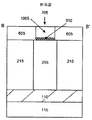
図6に示すように、例えば従来のたい積技術を使用して、ダミーゲート505上に絶縁層605を形成する。絶縁層605は、例えば、テトラエチルオルトシリケート(TEOS;TetraEthylOrthSilicate)を含んでいてよい。絶縁層605は、例えば約1000Åから約2500Åの厚みとすることができる。
図6に示すように、絶縁層605はその後、ダミーゲート505の上面を露出させるべく、例えば化学的機械的研磨(CMP)を使用して研磨される。
As shown in FIG. 6, an insulating
As shown in FIG. 6, the insulating
その後、図7に示すように、ゲートトレンチ705を残すように、ダミーゲート505およびダミー酸化膜405を除去することができる。例えば従来のエッチングプロセスを使用して、ダミーゲート505およびダミー酸化膜405を除去してよい。
図8に示すように、局所的に細型化されたフィン領域805を形成するように、ゲートトレンチ705内に露出したフィン・チャネルの部分を細型化することができる。例えばフィン・チャネルの選択エッチングによって、ゲートトレンチ705内に露出したフィン・チャネルの部分を細型化してよい。
その後、図9に示すように、ゲート絶縁膜910をゲートトレンチ705中に形成することができる。ゲート絶縁膜910は、従来のプロセスを使用して、熱成長またはたい積することができる。
ゲート絶縁膜910は、SiO、SiO2、SiN、SiON、HFO2、ZrO2、A12O3、HFSiO (x)、ZnS、MgF2、または他の高誘電率(high-k)の誘電材料を含み得る。
Thereafter, as shown in FIG. 7, the
As shown in FIG. 8, the portion of the fin channel exposed in the
Thereafter, as shown in FIG. 9, a
The
図10A、図10B、および図10Cに示すように、ゲート絶縁膜910上のゲートトレンチ705中に、金属ゲート1005を形成する。
金属ゲート1005は、例えば従来の金属たい積プロセスを使用して、ゲートトレンチ705中に形成され、絶縁層605の上面まで研磨される。
金属ゲート1005は、例えばTaNまたはTiNのような金属材料を含んでいてよいが、他の材料を使用することもできる。
図10Cに示すように、生成された金属ゲート1005はフィン205の3つの側面に配置され、したがって、トライゲートFinFETが製造される。
本発明の実施形態によるトライゲートFinFETは、ダブルゲートやシングルゲート・デバイスよりも、短チャネルをより制御することができる。トライゲートFinFETは、同じ領域における駆動電流が、ダブルゲートFinFETよりも高い。トライゲートFinFETの金属ゲート905はまた、ポリシリコン空乏効果およびゲート抵抗を低下させる。
As shown in FIGS. 10A, 10B, and 10C, a
A
The
As shown in FIG. 10C, the generated
Tri-gate FinFETs according to embodiments of the present invention can control the short channel more than double gate or single gate devices. The tri-gate FinFET has a higher drive current in the same region than the double-gate FinFET. The metal gate 905 of the tri-gate FinFET also reduces the polysilicon depletion effect and gate resistance.
[例示的な、異なる濃度でドープされた(differentially doped)モリブデンFinFETゲート]
図11および図12は、非対称のモリブデンFinFETゲートを形成する例示的なプロセスを示している。図11に示すように、例示的なプロセスは、モリブデン・スペーサ1110、1115を製造すべく、フィン1105上にモリブデンをたい積することから開始する。フィン1105は、図1および図2について上述した例示的なプロセスにより形成することができる。
モリブデン・スペーサ1110、1115の厚みは、例えば約200Åから約1500Åとすることができる。
[Exemplary, differentially doped molybdenum FinFET gates]
11 and 12 illustrate an exemplary process for forming an asymmetric molybdenum FinFET gate. As shown in FIG. 11, the exemplary process begins by depositing molybdenum on
The thickness of the
モリブデンのたい積に続いて、スペーサ1110、1115は、異なる濃度の窒素の注入により、非対称にドープされ得る。
スペーサ1110、1115における窒素の注入は、各スペーサに関連する仕事関数を変化させる。したがって、このスペーサ1110、1115の非対称ドーピングにより2つの仕事関数(dual work function)を有することとなり、形成されるFinFETにおける非対称ゲートを製造する。
Following the molybdenum deposition, the
The implantation of nitrogen in the
前述の明細書において、特定的な材料、構造、化学、プロセス等のような多くの特定的な詳細が記載されたが、本発明の完全な理解を与えるためである。しかし、本発明は本文に具体的に記載された詳細に頼ることなく実施可能である。他の例において、周知のプロセッシング構造は、本発明の趣旨を無駄にあいまいにしないために詳細が記載されていない。本発明を実施する際に従来のフォトリソグラフィおよびエッチング技術が利用され得、したがって、そのような技術の詳細は明細書に詳細に記載されていない。 In the foregoing specification, numerous specific details have been set forth, such as specific materials, structures, chemistry, processes, etc., in order to provide a thorough understanding of the present invention. However, the present invention can be practiced without resorting to the details specifically set forth herein. In other instances, well known processing structures have not been described in detail in order not to unnecessarily obscure the spirit of the invention. Conventional photolithography and etching techniques may be utilized in practicing the present invention, and details of such techniques are not described in detail in the specification.
本発明の好適な実施形態および本発明の多様な例のいくつかのみが示され、本開示に記載されている。本発明は多様な他の組み合わせおよび環境において使用可能であり、本文に表された進歩性の趣旨の範囲内で改変が可能である。 Only preferred embodiments of the invention and some of the various examples of the invention are shown and described in this disclosure. The present invention can be used in a variety of other combinations and environments and can be modified within the spirit of the inventive step expressed herein.
Claims (10)
前記フィンの第1端部上にソース領域、前記フィンの第2端部上にドレイン領域を形成するステップと、
前記フィン、前記ソース領域、および前記ドレイン領域の上面に、酸化物キャップを形成するステップと、
前記酸化物キャップの形成後に、前記フィン、前記ソース領域および前記ドレイン領域上に犠牲酸化層を形成するステップと、
前記フィンの表面から損傷部を除去すべく、前記犠牲酸化層を除去するステップと、
前記犠牲酸化層を除去した後に、前記フィン、前記ソース領域および前記ドレイン領域上にダミー酸化膜を形成し、前記フィン、前記ソース領域、前記ドレイン領域および前記ダミー酸化膜上にポリシリコン層を形成して該ポリシリコン層を研磨した後、前記ダミー酸化膜上に、第1パターンで、前記研磨されたポリシリコン層にエッチングされた第1半導体材料のダミーゲートを形成するステップと、
前記ダミーゲートの周りに絶縁層を形成するステップと、
前記第1パターンに対応する前記絶縁層中にトレンチを残すように、前記ダミー酸化膜および前記第1半導体材料を除去するステップと、
前記トレンチ内に露出した前記フィンの一部分を細型化するステップと、
前記トレンチ内に露出した前記フィンの前記表面にゲート絶縁層を形成するステップと、
前記ゲート絶縁層上の前記トレンチ内に金属ゲートを形成するステップと、を含む、
フィン電界効果トランジスタを形成する方法。 Forming a fin;
Forming a source region on the first end of the fin and a drain region on the second end of the fin;
Said fins, said source region, and the upper surface of the drain region, forming an oxide cap,
After formation of the oxide cap, forming a sacrificial oxide layer on the fin, the source region and the drain region,
Removing the sacrificial oxide layer to remove damage from the surface of the fin;
After removing the sacrificial oxide layer, a dummy oxide film is formed on the fin, the source region, and the drain region, and a polysilicon layer is formed on the fin, the source region, the drain region, and the dummy oxide film. Then, after polishing the polysilicon layer, forming a dummy gate of the first semiconductor material etched on the polished polysilicon layer in a first pattern on the dummy oxide film ;
Forming an insulating layer around the dummy gate;
Removing the dummy oxide film and the first semiconductor material to leave a trench in the insulating layer corresponding to the first pattern;
Thinning a portion of the fin exposed in the trench;
Forming a gate insulating layer on the surface of the fin exposed in the trench;
Forming a metal gate in the trench on the gate insulating layer.
A method of forming a fin field effect transistor.
前記第1パターンで前記ダミーゲートを形成するように、前記第1半導体材料の層をエッチングするステップと、を含む請求項7記載の方法。 Forming the dummy gate comprises depositing a layer of the first semiconductor material on the fin;
8. The method of claim 7, comprising: etching the layer of first semiconductor material to form the dummy gate with the first pattern.
前記犠牲酸化層を熱成長させるステップを含み、
前記犠牲酸化層を除去するステップは、前記フィンの表面から損傷部を除去するように、前記犠牲酸化層をエッチングするステップを含む、請求項1記載の方法。 Forming the sacrificial oxide layer comprises:
Thermally growing the sacrificial oxide layer;
The method of claim 1, wherein removing the sacrificial oxide layer comprises etching the sacrificial oxide layer to remove damage from a surface of the fin.
Applications Claiming Priority (3)
| Application Number | Priority Date | Filing Date | Title |
|---|---|---|---|
| US10/754,540 | 2004-01-12 | ||
| US10/754,540 US7186599B2 (en) | 2004-01-12 | 2004-01-12 | Narrow-body damascene tri-gate FinFET |
| PCT/US2004/043105 WO2005071727A1 (en) | 2004-01-12 | 2004-12-21 | Narrow-body damascene tri-gate finfet having thinned body |
Publications (3)
| Publication Number | Publication Date |
|---|---|
| JP2007518271A JP2007518271A (en) | 2007-07-05 |
| JP2007518271A5 JP2007518271A5 (en) | 2008-02-14 |
| JP5270094B2 true JP5270094B2 (en) | 2013-08-21 |
Family
ID=34739407
Family Applications (1)
| Application Number | Title | Priority Date | Filing Date |
|---|---|---|---|
| JP2006549311A Active JP5270094B2 (en) | 2004-01-12 | 2004-12-21 | Narrow body damascene tri-gate FinFET with thinned body |
Country Status (8)
| Country | Link |
|---|---|
| US (1) | US7186599B2 (en) |
| JP (1) | JP5270094B2 (en) |
| KR (1) | KR101066271B1 (en) |
| CN (1) | CN100505183C (en) |
| DE (1) | DE112004002633B4 (en) |
| GB (1) | GB2426124B (en) |
| TW (1) | TWI350002B (en) |
| WO (1) | WO2005071727A1 (en) |
Families Citing this family (26)
| Publication number | Priority date | Publication date | Assignee | Title |
|---|---|---|---|---|
| KR100574971B1 (en) * | 2004-02-17 | 2006-05-02 | 삼성전자주식회사 | Semiconductor device having multi-gate structure and method of manufacturing the same |
| WO2006076151A2 (en) * | 2004-12-21 | 2006-07-20 | Carnegie Mellon University | Lithography and associated methods, devices, and systems |
| US7323374B2 (en) * | 2005-09-19 | 2008-01-29 | International Business Machines Corporation | Dense chevron finFET and method of manufacturing same |
| KR100696197B1 (en) * | 2005-09-27 | 2007-03-20 | 한국전자통신연구원 | Multiple-gate MOS transistor using the Si substrate and a method for manufacturing the same |
| US7326976B2 (en) * | 2005-11-15 | 2008-02-05 | International Business Machines Corporation | Corner dominated trigate field effect transistor |
| US20070152266A1 (en) * | 2005-12-29 | 2007-07-05 | Intel Corporation | Method and structure for reducing the external resistance of a three-dimensional transistor through use of epitaxial layers |
| US7791140B2 (en) * | 2006-02-13 | 2010-09-07 | Nxp B.V. | Double-gate semiconductor devices having gates with different work functions and methods of manufacture thereof |
| WO2007133775A2 (en) * | 2006-05-15 | 2007-11-22 | Carnegie Mellon University | Integrated circuit, device, system, and method of fabrication |
| US7923337B2 (en) | 2007-06-20 | 2011-04-12 | International Business Machines Corporation | Fin field effect transistor devices with self-aligned source and drain regions |
| US20110147804A1 (en) * | 2009-12-23 | 2011-06-23 | Rishabh Mehandru | Drive current enhancement in tri-gate MOSFETS by introduction of compressive metal gate stress using ion implantation |
| TWI582999B (en) | 2011-03-25 | 2017-05-11 | 半導體能源研究所股份有限公司 | Field-effect transistor, and memory and semiconductor circuit including the same |
| CN102810476B (en) | 2011-05-31 | 2016-08-03 | 中国科学院微电子研究所 | The manufacture method of fin formula field effect transistor |
| CN103123899B (en) * | 2011-11-21 | 2015-09-30 | 中芯国际集成电路制造(上海)有限公司 | FinFET manufacture method |
| CN103123900B (en) * | 2011-11-21 | 2015-09-02 | 中芯国际集成电路制造(上海)有限公司 | FinFET manufacture method |
| CN103295899B (en) * | 2012-02-27 | 2016-03-30 | 中芯国际集成电路制造(上海)有限公司 | FinFET manufacture method |
| CN103456638B (en) * | 2012-06-05 | 2016-02-03 | 中芯国际集成电路制造(上海)有限公司 | Autoregistration GaAs FinFET structure and manufacture method thereof |
| US8652891B1 (en) * | 2012-07-25 | 2014-02-18 | The Institute of Microelectronics Chinese Academy of Science | Semiconductor device and method of manufacturing the same |
| CN103579315B (en) * | 2012-07-25 | 2017-03-08 | 中国科学院微电子研究所 | Semiconductor device and its manufacture method |
| US8847281B2 (en) * | 2012-07-27 | 2014-09-30 | Intel Corporation | High mobility strained channels for fin-based transistors |
| CN103681329B (en) * | 2012-09-10 | 2017-07-11 | 中国科学院微电子研究所 | Semiconductor devices and its manufacture method |
| KR101395026B1 (en) * | 2012-10-16 | 2014-05-15 | 경북대학교 산학협력단 | Nitride Semiconductor and Fabricating Method Thereof |
| CN103854982B (en) * | 2012-11-30 | 2016-09-28 | 中国科学院微电子研究所 | The manufacture method of semiconductor device |
| US9263554B2 (en) | 2013-06-04 | 2016-02-16 | International Business Machines Corporation | Localized fin width scaling using a hydrogen anneal |
| KR102072410B1 (en) | 2013-08-07 | 2020-02-03 | 삼성전자 주식회사 | Semiconductor device and fabricated method thereof |
| US9564445B2 (en) | 2014-01-20 | 2017-02-07 | International Business Machines Corporation | Dummy gate structure for electrical isolation of a fin DRAM |
| CN105632936B (en) * | 2016-03-22 | 2018-10-16 | 上海华力微电子有限公司 | A kind of preparation method of bigrid fin formula field effect transistor |
Family Cites Families (19)
| Publication number | Priority date | Publication date | Assignee | Title |
|---|---|---|---|---|
| US6225173B1 (en) | 1998-11-06 | 2001-05-01 | Advanced Micro Devices, Inc. | Recessed channel structure for manufacturing shallow source/drain extensions |
| US6365465B1 (en) | 1999-03-19 | 2002-04-02 | International Business Machines Corporation | Self-aligned double-gate MOSFET by selective epitaxy and silicon wafer bonding techniques |
| US6483156B1 (en) | 2000-03-16 | 2002-11-19 | International Business Machines Corporation | Double planar gated SOI MOSFET structure |
| FR2810157B1 (en) * | 2000-06-09 | 2002-08-16 | Commissariat Energie Atomique | METHOD FOR PRODUCING AN ELECTRONIC COMPONENT WITH SOURCE, DRAIN AND SELF-ALLOCATED GRID, IN DAMASCENE ARCHITECTURE |
| JP4058751B2 (en) * | 2000-06-20 | 2008-03-12 | 日本電気株式会社 | Method for manufacturing field effect transistor |
| US6413802B1 (en) | 2000-10-23 | 2002-07-02 | The Regents Of The University Of California | Finfet transistor structures having a double gate channel extending vertically from a substrate and methods of manufacture |
| US6472258B1 (en) | 2000-11-13 | 2002-10-29 | International Business Machines Corporation | Double gate trench transistor |
| US6475890B1 (en) | 2001-02-12 | 2002-11-05 | Advanced Micro Devices, Inc. | Fabrication of a field effect transistor with an upside down T-shaped semiconductor pillar in SOI technology |
| US6475869B1 (en) | 2001-02-26 | 2002-11-05 | Advanced Micro Devices, Inc. | Method of forming a double gate transistor having an epitaxial silicon/germanium channel region |
| JP3543117B2 (en) * | 2001-03-13 | 2004-07-14 | 独立行政法人産業技術総合研究所 | Double gate field effect transistor |
| FR2822293B1 (en) | 2001-03-13 | 2007-03-23 | Nat Inst Of Advanced Ind Scien | FIELD EFFECT TRANSISTOR AND DOUBLE GRID, INTEGRATED CIRCUIT COMPRISING THIS TRANSISTOR, AND METHOD OF MANUFACTURING THE SAME |
| US6635923B2 (en) | 2001-05-24 | 2003-10-21 | International Business Machines Corporation | Damascene double-gate MOSFET with vertical channel regions |
| US20030025167A1 (en) * | 2001-07-31 | 2003-02-06 | International Business Machines Corporation | Activating in-situ doped gate on high dielectric constant materials |
| US6583469B1 (en) * | 2002-01-28 | 2003-06-24 | International Business Machines Corporation | Self-aligned dog-bone structure for FinFET applications and methods to fabricate the same |
| US6642090B1 (en) | 2002-06-03 | 2003-11-04 | International Business Machines Corporation | Fin FET devices from bulk semiconductor and method for forming |
| US6762483B1 (en) | 2003-01-23 | 2004-07-13 | Advanced Micro Devices, Inc. | Narrow fin FinFET |
| US6787854B1 (en) | 2003-03-12 | 2004-09-07 | Advanced Micro Devices, Inc. | Method for forming a fin in a finFET device |
| US6764884B1 (en) | 2003-04-03 | 2004-07-20 | Advanced Micro Devices, Inc. | Method for forming a gate in a FinFET device and thinning a fin in a channel region of the FinFET device |
| US6855989B1 (en) * | 2003-10-01 | 2005-02-15 | Advanced Micro Devices, Inc. | Damascene finfet gate with selective metal interdiffusion |
-
2004
- 2004-01-12 US US10/754,540 patent/US7186599B2/en active Active
- 2004-12-21 DE DE112004002633T patent/DE112004002633B4/en active Active
- 2004-12-21 GB GB0615126A patent/GB2426124B/en active Active
- 2004-12-21 CN CNB2004800403026A patent/CN100505183C/en active Active
- 2004-12-21 WO PCT/US2004/043105 patent/WO2005071727A1/en active Application Filing
- 2004-12-21 JP JP2006549311A patent/JP5270094B2/en active Active
- 2004-12-21 KR KR1020067013974A patent/KR101066271B1/en active IP Right Grant
-
2005
- 2005-01-11 TW TW094100703A patent/TWI350002B/en active
Also Published As
| Publication number | Publication date |
|---|---|
| CN1902741A (en) | 2007-01-24 |
| DE112004002633B4 (en) | 2008-12-24 |
| TWI350002B (en) | 2011-10-01 |
| US7186599B2 (en) | 2007-03-06 |
| GB2426124A (en) | 2006-11-15 |
| TW200529433A (en) | 2005-09-01 |
| CN100505183C (en) | 2009-06-24 |
| KR101066271B1 (en) | 2011-09-21 |
| US20050153485A1 (en) | 2005-07-14 |
| GB0615126D0 (en) | 2006-09-06 |
| DE112004002633T5 (en) | 2007-01-04 |
| GB2426124B (en) | 2007-12-12 |
| JP2007518271A (en) | 2007-07-05 |
| WO2005071727A1 (en) | 2005-08-04 |
| KR20060123480A (en) | 2006-12-01 |
Similar Documents
| Publication | Publication Date | Title |
|---|---|---|
| JP5270094B2 (en) | Narrow body damascene tri-gate FinFET with thinned body | |
| US9978870B2 (en) | FinFET with buried insulator layer and method for forming | |
| US7541267B1 (en) | Reversed T-shaped finfet | |
| JP5009611B2 (en) | Method for forming a structure in a FINFET device | |
| JP5409997B2 (en) | Method for forming a gate in a FinFET device and method for manufacturing a semiconductor device | |
| US6645797B1 (en) | Method for forming fins in a FinFET device using sacrificial carbon layer | |
| US6855583B1 (en) | Method for forming tri-gate FinFET with mesa isolation | |
| US6872647B1 (en) | Method for forming multiple fins in a semiconductor device | |
| US7084018B1 (en) | Sacrificial oxide for minimizing box undercut in damascene FinFET | |
| US6686231B1 (en) | Damascene gate process with sacrificial oxide in semiconductor devices | |
| JP4745663B2 (en) | Method for forming a double gate Fin-FET device | |
| US6709982B1 (en) | Double spacer FinFET formation | |
| US6812119B1 (en) | Narrow fins by oxidation in double-gate finfet | |
| US6998301B1 (en) | Method for forming a tri-gate MOSFET | |
| US6855989B1 (en) | Damascene finfet gate with selective metal interdiffusion | |
| JP2006516821A (en) | Method for forming strained channel fin FET | |
| JP2006505950A (en) | Double-gate semiconductor device having multiple separated gates | |
| US20170229452A1 (en) | Fin field effect transistor and method for fabricating the same | |
| JP2006505949A (en) | Planarization of gate materials to improve the critical dimensions of semiconductor device gates. | |
| JP2007500456A (en) | Multi-step chemical mechanical polishing of gate region in FINFET | |
| KR20140099212A (en) | Methods of forming fins for a finfet semiconductor device using a mandrel oxidation process | |
| JP5270093B2 (en) | Tri-gate FinFET formed by damascene process | |
| US6876042B1 (en) | Additional gate control for a double-gate MOSFET | |
| US6967175B1 (en) | Damascene gate semiconductor processing with local thinning of channel region | |
| CN110233108B (en) | Fence device and manufacturing method thereof |
Legal Events
| Date | Code | Title | Description |
|---|---|---|---|
| A521 | Request for written amendment filed |
Free format text: JAPANESE INTERMEDIATE CODE: A523 Effective date: 20071221 |
|
| A621 | Written request for application examination |
Free format text: JAPANESE INTERMEDIATE CODE: A621 Effective date: 20071221 |
|
| RD03 | Notification of appointment of power of attorney |
Free format text: JAPANESE INTERMEDIATE CODE: A7423 Effective date: 20100421 |
|
| RD05 | Notification of revocation of power of attorney |
Free format text: JAPANESE INTERMEDIATE CODE: A7425 Effective date: 20100902 |
|
| A131 | Notification of reasons for refusal |
Free format text: JAPANESE INTERMEDIATE CODE: A131 Effective date: 20110921 |
|
| A977 | Report on retrieval |
Free format text: JAPANESE INTERMEDIATE CODE: A971007 Effective date: 20110922 |
|
| A601 | Written request for extension of time |
Free format text: JAPANESE INTERMEDIATE CODE: A601 Effective date: 20111216 |
|
| A602 | Written permission of extension of time |
Free format text: JAPANESE INTERMEDIATE CODE: A602 Effective date: 20111226 |
|
| A601 | Written request for extension of time |
Free format text: JAPANESE INTERMEDIATE CODE: A601 Effective date: 20120123 |
|
| A602 | Written permission of extension of time |
Free format text: JAPANESE INTERMEDIATE CODE: A602 Effective date: 20120130 |
|
| A521 | Request for written amendment filed |
Free format text: JAPANESE INTERMEDIATE CODE: A523 Effective date: 20120221 |
|
| A02 | Decision of refusal |
Free format text: JAPANESE INTERMEDIATE CODE: A02 Effective date: 20120822 |
|
| A521 | Request for written amendment filed |
Free format text: JAPANESE INTERMEDIATE CODE: A523 Effective date: 20121225 |
|
| A911 | Transfer to examiner for re-examination before appeal (zenchi) |
Free format text: JAPANESE INTERMEDIATE CODE: A911 Effective date: 20130225 |
|
| TRDD | Decision of grant or rejection written | ||
| A01 | Written decision to grant a patent or to grant a registration (utility model) |
Free format text: JAPANESE INTERMEDIATE CODE: A01 Effective date: 20130501 |
|
| A61 | First payment of annual fees (during grant procedure) |
Free format text: JAPANESE INTERMEDIATE CODE: A61 Effective date: 20130509 |
|
| R150 | Certificate of patent or registration of utility model |
Free format text: JAPANESE INTERMEDIATE CODE: R150 Ref document number: 5270094 Country of ref document: JP Free format text: JAPANESE INTERMEDIATE CODE: R150 |
|
| R250 | Receipt of annual fees |
Free format text: JAPANESE INTERMEDIATE CODE: R250 |
|
| R250 | Receipt of annual fees |
Free format text: JAPANESE INTERMEDIATE CODE: R250 |
|
| R250 | Receipt of annual fees |
Free format text: JAPANESE INTERMEDIATE CODE: R250 |
|
| R250 | Receipt of annual fees |
Free format text: JAPANESE INTERMEDIATE CODE: R250 |
|
| R250 | Receipt of annual fees |
Free format text: JAPANESE INTERMEDIATE CODE: R250 |
|
| R250 | Receipt of annual fees |
Free format text: JAPANESE INTERMEDIATE CODE: R250 |
|
| R250 | Receipt of annual fees |
Free format text: JAPANESE INTERMEDIATE CODE: R250 |
|
| R250 | Receipt of annual fees |
Free format text: JAPANESE INTERMEDIATE CODE: R250 |