JP5257238B2 - Manufacturing information management method for printed wiring board, manufacturing information management system for printed wiring board - Google Patents
Manufacturing information management method for printed wiring board, manufacturing information management system for printed wiring board Download PDFInfo
- Publication number
- JP5257238B2 JP5257238B2 JP2009123284A JP2009123284A JP5257238B2 JP 5257238 B2 JP5257238 B2 JP 5257238B2 JP 2009123284 A JP2009123284 A JP 2009123284A JP 2009123284 A JP2009123284 A JP 2009123284A JP 5257238 B2 JP5257238 B2 JP 5257238B2
- Authority
- JP
- Japan
- Prior art keywords
- tag
- printed wiring
- state
- information
- sheet
- Prior art date
- Legal status (The legal status is an assumption and is not a legal conclusion. Google has not performed a legal analysis and makes no representation as to the accuracy of the status listed.)
- Expired - Fee Related
Links
Images


Landscapes
- Structure Of Printed Boards (AREA)
- Supply And Installment Of Electrical Components (AREA)
Description
本発明は、プリント配線基板の製造工程における製造履歴等の情報を管理するプリント配線基板の製造情報管理方法、プリント配線基板の製造情報管理システムに関するものである。 The present invention relates to a printed wiring board manufacturing information management method and a printed wiring board manufacturing information management system for managing information such as manufacturing history in a printed wiring board manufacturing process.
様々な製品の製造工程等において、その製造履歴に関する情報を、製品や製品を収納する筐体等に取り付けられたRFID(Radio Frequency Identification)タグを用いて管理する技術は、既に多数提案されている。 A number of techniques for managing information related to manufacturing history in various product manufacturing processes using RFID (Radio Frequency Identification) tags attached to a product or a housing for storing the product have already been proposed. .
従来のバーコードやID番号を製品等に印字したり、バーコード等が記載されたシールを製品等に貼着したりするといった方法では、印字が消えたり、シールが剥離したりして追跡が不可能となるといった問題に加えて、情報の追加や更新を行うことができないといった問題があった。
これに対して、上述のようなRFIDタグを用いた製造履歴等に関する情報を管理する管理システムは、情報の更新や追記が容易であるという利点を有しており、様々な分野で利用されており、プリント配線基板の製造工程においても使用されている(例えば、特許文献1)。
With conventional methods such as printing barcodes and ID numbers on products, etc., or sticking stickers with barcodes on products, etc., the prints disappear or the seals are peeled off for tracking. In addition to the problem of being impossible, there was a problem that information could not be added or updated.
On the other hand, the management system for managing information related to the manufacturing history using the RFID tag as described above has an advantage that it is easy to update or add information, and is used in various fields. It is also used in the manufacturing process of printed wiring boards (for example, Patent Document 1).
特許文献1に示すように、プリント配線基板1つ1つにICタグを装着する場合には、1つ1つのプリント配線基板ごとの情報管理を行うことができる。
しかしながら、携帯電話等の小型製品に用いられるプリント配線基板は小型であるために、小型化されたICタグといえども実装するための面積を設けることは、設計上容易ではない。また、非常に多数のプリント配線基板にICタグを設けることになるため、コストや作業時間等の面からも現実的ではない。
さらに、このような方法では、プリント配線基板の製造以後の工程(例えば、基板への部材の実装工程や、製品への組み込み工程等)を、納入先等において別の管理システム等で管理する場合には、基板の製造工程で使用したICタグは不要となる。また、そもそも、製造履歴を管理するICタグを付けたまま製品化することは、好ましくない。そのため、プリント配線基板の出荷前等に、個々のICタグを回収する作業が必要になるという問題がある。
As shown in
However, since a printed wiring board used for a small product such as a cellular phone is small, it is not easy in design to provide an area for mounting even a miniaturized IC tag. Further, since IC tags are provided on a very large number of printed wiring boards, it is not realistic from the viewpoint of cost, working time, and the like.
Furthermore, in such a method, the process after the production of the printed wiring board (for example, the process of mounting a member on the board, the process of incorporating the product into the product, etc.) is managed by another management system or the like at the delivery destination. Therefore, the IC tag used in the substrate manufacturing process is not necessary. In the first place, it is not preferable to produce a product with an IC tag for managing the manufacturing history. Therefore, there is a problem that it is necessary to collect individual IC tags before shipping the printed wiring board.
本発明の課題は、情報量が大きく、かつ、製造工程の下流からも上流からも製造履歴等に関する情報を追跡可能なプリント配線基板の製造情報管理方法、プリント配線基板の製造情報管理システムを提供することである。 SUMMARY OF THE INVENTION An object of the present invention is to provide a printed wiring board manufacturing information management method and a printed wiring board manufacturing information management system capable of tracking information related to manufacturing history and the like from a downstream and upstream manufacturing process. It is to be.
本発明は、以下のような解決手段により、前記課題を解決する。なお、理解を容易にするために、本発明の実施形態に対応する符号を付して説明するが、これに限定されるものではない。
請求項1の発明は、第1の状態(10,20)から第2の状態(20,30)へ加工する加工工程(S111,S115)を有するプリント配線基板の製造工程における製造情報を管理するプリント配線基板の製造情報管理方法であって、前記第1の状態(10,20)は、書き込み可能なメモリを有する非接触通信可能な第1のICタグ(12,22)を備え、前記第2の状態(20,30)は、書き込み可能なメモリを有する非接触通信可能な第2のICタグ(22,42)を備えており、前記第1のICタグに記録されている第1情報を前記第2のICタグに書き込み、かつ、前記第2のICタグに記録されている第2情報を、前記第1のICタグに書き込む情報書き写し工程(S110,S114)を備えること、を特徴とするプリント配線基板の製造情報管理方法である。
請求項2の発明は、請求項1に記載のプリント配線基板の製造情報管理方法において、前記第1の状態(10,20)は、前記第2の状態である第2基板(20,30)を、第1保持枠(11,21)により複数保持している状態であり、前記第1のICタグは、前記第1保持枠に設けられていること、を特徴とするプリント配線基板の製造情報管理方法である。
請求項3の発明は、請求項1又は請求項2に記載のプリント配線基板の製造情報管理方法において、前記第2の状態(20)は、第3の状態である第3基板(30)を、第2保持枠(21)により複数保持している状態であり、前記第2のICタグ(22)は、前記第2保持枠に設けられていること、を特徴とするプリント配線基板の製造情報管理方法である。
請求項4の発明は、請求項1又は請求項2に記載のプリント配線基板の製造情報管理方法において、前記第2の状態(30)は、収納部材(40)に単位基板(30)が1つ以上収納された状態であり、前記第2のICタグ(42)は、前記収納部材に設けられていること、を特徴とするプリント配線基板の製造情報管理方法である。
The present invention solves the above problems by the following means. In addition, in order to make an understanding easy, although the code | symbol corresponding to embodiment of this invention is attached | subjected and demonstrated, it is not limited to this.
The invention of
A second aspect of the present invention is the printed circuit board manufacturing information management method according to the first aspect, wherein the first state (10, 20) is the second state (20, 30). The first holding frame (11, 21) holds a plurality of the first IC tags, and the first IC tag is provided on the first holding frame. Information management method.
According to a third aspect of the present invention, in the printed circuit board manufacturing information management method according to the first or second aspect, the second state (20) includes a third substrate (30) which is a third state. A plurality of second holding frames (21) are held, and the second IC tag (22) is provided on the second holding frame. Information management method.
According to a fourth aspect of the present invention, in the printed circuit board manufacturing information management method according to the first or second aspect, in the second state (30), the unit board (30) is 1 in the housing member (40). The printed circuit board manufacturing information management method is characterized in that two or more second IC tags (42) are stored in the storage member.
請求項5の発明は、請求項1から請求項4までのいずれか1項に記載のプリント配線基板の製造情報管理方法において、前記加工工程(S111,S115)は、前記第1の状態(10,20)から前記第2の状態(20,30)へ切り出す切り出し工程(S111,S115)であること、を特徴とするプリント配線基板の製造情報管理方法である。
請求項6の発明は、請求項1から請求項5までのいずれか1項に記載のプリント配線基板の製造情報管理方法において、前記第1情報は、前記第1のICタグのユニークIDを含み、前記第2情報は、前記第2のICタグ(22,42)のユニークIDを含むこと、を特徴とするプリント配線基板の製造情報管理方法である。
請求項7の発明は、請求項1から請求項6までのいずれか1項に記載のプリント配線基板の製造情報管理方法において、前記加工工程(S111,S115)の前に、前記第1の状態の品質を検査する検査工程(S107,S108、S112,S113)を備え、前記第1情報は、前記第1のICタグ(12,22)のユニークIDと、前記第1の状態(10,20)の性能検査の検査結果に関する情報とを備えること、を特徴とするプリント配線基板の製造情報管理方法である。
請求項8の発明は、請求項1から請求項7までのいずれか1項に記載のプリント配線基板の製造情報管理方法において、前記第1のICタグ(12,22)及び前記第2のICタグ(22,42)に記録される情報が、管理サーバ(S1)に記録されるサーバ記録工程を有すること、を特徴とするプリント配線基板の製造情報管理方法である。
According to a fifth aspect of the present invention, in the printed circuit board manufacturing information management method according to any one of the first to fourth aspects, the processing steps (S111, S115) include the first state (10 , 20) is a cut-out process (S111, S115) for cutting out from the second state (20, 30) to the printed circuit board manufacturing information management method.
The invention of claim 6 is the manufacturing information management method for a printed wiring board according to any one of
The invention of claim 7 is the manufacturing information management method for a printed wiring board according to any one of
The invention of claim 8 is the manufacturing information management method for a printed wiring board according to any one of
請求項9の発明は、第1の状態(10,20)から第2の状態(20,30)へ加工する加工工程(S111,S115)を有するプリント配線基板の製造工程における製造情報を管理するプリント配線基板の製造情報管理システムであって、前記第1の状態が有し、非接触通信可能であって書き込み可能なメモリを有する第1のICタグ(12,22)と、前記第2の状態が有し、非接触通信可能であって書き込み可能なメモリを有する第2のICタグ(22,42)と、前記第1のICタグに記録された第1情報を読み取る第1読み取り部(51、52)と、読み取られた前記第1情報を前記第2のICタグに書き込む第2書き込み部(52,53)と、前記第2のICタグに記録された第2情報を読み取る第2読み取り部(52,53)と、読み取った前記第2情報を前記第1のICタグに書き込む第1書き込み部(51,52)と、前記第1読み取り部、前記第2読み取り部、前記第1書き込み部、前記第2書き込み部の動作を制御する制御部(80)と、を備えること、を特徴とするプリント配線基板の製造情報管理システムである。
請求項10の発明は、請求項9に記載のプリント配線基板の製造情報管理システムにおいて、前記第1のICタグ(12,22)及び前記第2のICタグ(22,42)に記録される情報を記録する管理部(S1)を備えること、を特徴とするプリント配線基板の製造情報管理システムである。
請求項11の発明は、請求項9又は請求項10に記載のプリント配線基板の製造情報管理システムにおいて、前記第1の状態(10,20)、前記第2の状態(20,30)の性能を検査する検査部(61,62,63,71,72)を備えること、を特徴とするプリント配線基板の製造情報管理システムである。
The invention of claim 9 manages manufacturing information in a manufacturing process of a printed wiring board having processing steps (S111, S115) for processing from the first state (10, 20) to the second state (20, 30). A printed circuit board manufacturing information management system, comprising: a first IC tag (12, 22) having a memory capable of being contactlessly communicated and writable in the first state; A second IC tag (22, 42) having a state and capable of non-contact communication and having a writable memory; and a first reading unit (1) for reading first information recorded on the
The invention of
The invention of
本発明によれば、以下の効果を奏することができる。
(1)本発明によるプリント配線基板の製造情報管理方法は、第1のICタグに記録されている第1情報を第2のICタグに書き込み、かつ、第2のICタグに記録されている第2情報を、第1のICタグに書き込む情報書き写し工程を備えるので、第2の状態側からも第1の状態側からも、すなわち、製造工程における上流側からも下流側からも、プリント配線基板の製造情報を追跡することが可能となり、プリント配線基板の製造履歴等の製造に関する情報をICタグによって効率よく管理することができる。また、情報書き写し工程を備えることにより、ICタグによってプリント配線基板の製造情報を管理できるので、サーバを用意しなくとも情報管理を行うことができ、コスト低減を図ることができる。
According to the present invention, the following effects can be obtained.
(1) In the printed wiring board manufacturing information management method according to the present invention, the first information recorded in the first IC tag is written in the second IC tag, and is recorded in the second IC tag. Since there is an information copying process for writing the second information to the first IC tag, it is possible to print from both the second state side and the first state side, that is, from the upstream side and the downstream side in the manufacturing process. The manufacturing information of the board can be traced, and information related to manufacturing such as the manufacturing history of the printed wiring board can be efficiently managed by the IC tag. In addition, by providing the information copying step, manufacturing information of the printed wiring board can be managed by the IC tag, so that information management can be performed without preparing a server, and costs can be reduced.
(2)第1の状態は、第2の状態である第2基板を、第1保持枠により複数保持している状態であり、第1のICタグは、第1保持枠に設けられている。従って、第1基板から第2基板へと加工した後に残される第1保持枠に第1のICタグが設けられているので、個々の第2基板内にICタグを配置するための設計等が不要となり、製造が容易である。また、第2基板からICタグを取り外す作業が不要となり、作業効率を向上できる。 (2) The first state is a state in which a plurality of second substrates in the second state are held by the first holding frame, and the first IC tag is provided on the first holding frame. . Therefore, since the first IC tag is provided in the first holding frame that is left after processing from the first substrate to the second substrate, the design for arranging the IC tag in each second substrate is possible. It becomes unnecessary and easy to manufacture. Moreover, the work of removing the IC tag from the second substrate is not necessary, and the work efficiency can be improved.
(3)第2の状態は、第3の状態である第3基板を、第2保持枠により複数保持している状態であり、第2のICタグは、第2保持枠に設けられている。従って、第2基板から第3基板へと加工した後に残される第2保持枠に第2のICタグが設けられているので、個々の第3基板内にICタグを配置するための設計等が不要となり、製造が容易である。また、第3基板からICタグを取り外す作業が不要となり、作業効率が向上する。 (3) The second state is a state where a plurality of third substrates, which are the third state, are held by the second holding frame, and the second IC tag is provided on the second holding frame. . Accordingly, since the second IC tag is provided in the second holding frame that is left after processing from the second substrate to the third substrate, a design for arranging the IC tag in each third substrate is possible. It becomes unnecessary and easy to manufacture. Moreover, the work of removing the IC tag from the third substrate is not necessary, and the work efficiency is improved.
(4)第2の状態は、収納部材に単位基板が1つ以上収納された状態であり、第2のICタグは、収納部材に設けられているので、個々の単位基板内にICタグを設けるための設計等が不要となり、製造が容易である。また、単位基板からICタグを取り外す作業が不要となるので、作業効率が向上する。 (4) The second state is a state in which one or more unit substrates are stored in the storage member, and the second IC tag is provided in the storage member, so that the IC tag is placed in each unit substrate. The design and the like for providing are unnecessary, and the manufacturing is easy. In addition, the work efficiency is improved because the work of removing the IC tag from the unit substrate is not required.
(5)加工工程は、第1の状態から第2の状態へ切り出す切り出し工程であるので、第1の状態から切り出されて、すなわち、分離されて第2の状態となり次工程へと進んだ場合にも、第2のICタグは第1の状態の第1情報を保持し、第1のICタグは第2の状態の第2情報を保持できる。 (5) Since the processing step is a cutting step for cutting out from the first state to the second state, the cutting step is cut out from the first state, that is, separated into the second state and proceeding to the next step In addition, the second IC tag can hold the first information in the first state, and the first IC tag can hold the second information in the second state.
(6)第1情報は、第1のICタグのユニークIDを含み、第2情報は、第2のICタグのユニークIDを含むので、それぞれのユニークIDを追跡することにより、プリント配線基板の製造情報を追跡することが可能である。 (6) Since the first information includes the unique ID of the first IC tag, and the second information includes the unique ID of the second IC tag, by tracking each unique ID, the printed circuit board Manufacturing information can be tracked.
(7)加工工程の前に、第1の状態の品質を検査する検査工程を備え、第1情報は、第1のICタグのユニークIDと、第1の状態の性能検査の検査結果に関する情報とを備えるので、ユニークIDを追跡することによりプリント配線基板の製造情報を追跡することが可能となることに加え、検査結果の情報等のより詳細なプリント配線基板の製造情報を管理することができる。 (7) An inspection step for inspecting the quality of the first state is provided before the processing step, and the first information is information related to the unique ID of the first IC tag and the inspection result of the performance inspection of the first state. Therefore, it is possible to track the manufacturing information of the printed wiring board by tracking the unique ID, and manage more detailed manufacturing information of the printed wiring board such as information on the inspection result. it can.
(8)第1のICタグ及び第2のICタグに記録される情報が、管理サーバに記録されるサーバ記録工程を有するので、万が一、第1のICタグや第2のICタグが破損する等によって各ICタグに記録された情報が読み出せなくなったとしても、管理サーバから所望の情報を得ることができる。 (8) Since the information recorded in the first IC tag and the second IC tag includes a server recording process in which the information is recorded in the management server, the first IC tag and the second IC tag are damaged by any chance. Even if information recorded on each IC tag cannot be read due to the above, desired information can be obtained from the management server.
(9)本発明によるプリント配線基板の管理システムは、非接触通信可能であって書き込み可能なメモリを有する第1のICタグと、非接触通信可能であって書き込み可能なメモリを有する第2のICタグと、第1のICタグに記録された第1情報を読み取る第1読み取り部と、読み取られた第1情報を第2のICタグに書き込む第2書き込み部と、第2のICタグに記録された第2情報を読み取る第2読み取り部と、読み取った第2情報を第1のICタグに書き込む第1書き込み部と、第1読み取り部、第2読み取り部、第1書き込み部、第2書き込み部の動作を制御する制御部とを備えるので、製造工程における上流側からも下流側からも、プリント配線基板の製造情報を追跡可能である。 (9) A printed wiring board management system according to the present invention includes a first IC tag having a writable memory capable of contactless communication and a second IC having a writable memory capable of contactless communication. An IC tag, a first reading unit for reading the first information recorded on the first IC tag, a second writing unit for writing the read first information on the second IC tag, and a second IC tag A second reading unit for reading the recorded second information, a first writing unit for writing the read second information to the first IC tag, a first reading unit, a second reading unit, a first writing unit, a second And a control unit that controls the operation of the writing unit, the manufacturing information of the printed wiring board can be traced from the upstream side and the downstream side in the manufacturing process.
(10)第1のICタグ及び第2のICタグに記録される情報を記録する管理部を備えるので、万が一、第1のICタグや第2のICタグが破損する等により、記録された情報が読み出せなくなった場合にも、管理部から必要な情報を得ることができる。 (10) Since a management unit for recording information recorded in the first IC tag and the second IC tag is provided, the information was recorded due to the damage of the first IC tag or the second IC tag. Even when information cannot be read out, necessary information can be obtained from the management unit.
(11)第1の状態、第2の状態の性能を検査する検査部を備えるので、検査部によって検査された検査結果をICタグに記録させることができる。従って、より詳細なプリント配線基板の製造情報を管理することができる。 (11) Since the inspection unit that inspects the performance of the first state and the second state is provided, the inspection result inspected by the inspection unit can be recorded on the IC tag. Therefore, more detailed printed circuit board manufacturing information can be managed.
以下、本発明の実施形態を、図面等を参照しながら詳細に説明する。
なお、図1を含め、以下に示す各図は、模式的に示した図であり、各部の大きさ、形状は、理解を容易にするために、適宜誇張している。
また、本明細書中に記載する各部材の寸法や個数等は、実施形態としての一例であり、これに限定されるものではなく、適宜選択して使用してよい。
Hereinafter, embodiments of the present invention will be described in detail with reference to the drawings.
In addition, each figure shown below including FIG. 1 is the figure shown typically, and the magnitude | size and shape of each part are exaggerated suitably for easy understanding.
Moreover, the dimension, the number, and the like of each member described in the present specification are examples of the embodiment, and are not limited thereto, and may be appropriately selected and used.
(第1実施形態)
図1は、第1実施形態のプリント配線基板の製造情報管理システムを説明する図である。
本実施形態のプリント配線基板の製造情報管理システムは、ICタグ12,22,42と、このICタグ12,22,42と非接触通信可能なリーダライタ50(51〜53)と、光学検査装置60(61〜63)、電気的検査装置70(71,72)等と、CPU(Central Processing Unit 中央演算処理装置)80とを備えている。このプリント配線基板の製造方法管理システムは、プリント配線基板を製造し、所定の状態に加工して出荷するまでの製造履歴等の情報を管理するものである。
ICタグ12,22,42は、プリント配線基板の製造工程における各状態にそれぞれ設けられたRFIDタグであり、リーダライタ50と非接触通信によって情報の書き込みや読み出しが可能である。このICタグ12,22,42の詳細は、後述する。
リーダライタ50(51〜53)は、CPU80の指示により、各ICタグ12,22,42と非接触通信を行い、情報の書き込みや読み出し等を行う装置である。
(First embodiment)
FIG. 1 is a diagram illustrating a printed wiring board manufacturing information management system according to the first embodiment.
The printed wiring board manufacturing information management system according to the present embodiment includes an
The IC tags 12, 22, and 42 are RFID tags provided in each state in the printed wiring board manufacturing process, and can write and read information by contactless communication with the reader / writer 50. Details of the IC tags 12, 22, and 42 will be described later.
The reader / writer 50 (51 to 53) is a device that performs non-contact communication with each of the IC tags 12, 22, and 42 to write and read information according to instructions from the
光学検査装置60(61〜63)は、プリント配線基板の各状態において、その外観等を光学的に検査する検査部である。
電気的検査装置70(71,72)は、プリント配線基板の各状態において、所定の電気的な検査を行う検査部である。
CPU80は、光学検査装置60、電気的検査装置70、リーダライタ50等の動作を制御する制御部であり、光学検査装置60等の動作を制御するためのプログラム等を記憶するメモリ81を備えている。
The optical inspection device 60 (61 to 63) is an inspection unit that optically inspects the appearance and the like of each state of the printed wiring board.
The electrical inspection device 70 (71, 72) is an inspection unit that performs a predetermined electrical inspection in each state of the printed wiring board.
The
本実施形態のプリント配線基板の製造情報管理システムで管理されるプリント配線基板は、製品に組み込まれる単位基板30が複数形成されたシート状基板20を多面付けしたパネル状基板10を製造した後に、シート状基板20をパネル状基板10から切り出して所定の性能検査等を行い、シート状基板20から単位基板30を切り出して単位基板30を所定の容器(トレイ)40に収納して出荷するという製造工程をとっている。
また、単位基板30は、一例として、携帯電話に用いられるものであるとする。
The printed wiring board managed by the printed wiring board manufacturing information management system of the present embodiment is manufactured after manufacturing the panel-
The
まず、プリント配線基板の製造工程における各状態を説明する。
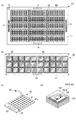
図2は、パネル状基板、シート状基板、単位基板の各状態でのプリント配線基板、及び、ICタグを示す図である。
パネル状基板10は、略平板状であり、複数のシート状基板20と、このシート状基板20を保持するパネル枠11と、パネル枠11に設けられたパネルICタグ12等を有した第1の状態でのプリント配線基板である(図2(a)参照)。
1つのパネル状基板10内に形成される複数のシート状基板20は、同一仕様であって同一形態となっている。本実施形態では、図2に示すように、1枚のパネル状基板10には、15枚のシート状基板20が多面付けされた状態となっている。
First, each state in the manufacturing process of the printed wiring board will be described.
FIG. 2 is a diagram showing a printed wiring board and an IC tag in each state of a panel-like board, a sheet-like board, and a unit board.
The panel-
A plurality of sheet-
また、本実施形態のパネル状基板10は、回路がパターン形成された不図示の4層のパターン形成層と、各パターン形成層の間に設けられた不図示の3枚の絶縁層(絶縁基板)とを備える多層構造であり、各絶縁層間は所定の位置に形成されたスルーホール等によって導通が確保されている形態となっている。
パネル枠11は、複数のシート状基板20を同一平面上に一体に保持する部分であり、この部分には、製品等に使用されるプリント配線基板(単位基板30)は形成されない。また、パネル枠11には、所定の位置に、パネルICタグ12や、テスト領域13、パネル情報表示領域14等が設けられている。
Further, the panel-
The
パネルICタグ12は、リーダライタ50等の外部機器と非接触通信可能なICタグであり、主として、パネル状基板10に関する情報を管理する機能を有している。
パネルICタグ12は、例えば、特開2007−213514号公報に開示されるような多層基板型のICタグであり、図2(d)に示すように、絶縁基板101上に形成されたアンテナ部102と、アンテナ部102を介してリーダライタ50等と非接触通信を行い、所定のコマンドを実行するICチップ103とを備え、ICチップ103には、書き込み可能なメモリを有している。
このパネルICタグ12は、メモリの所定の領域に、そのパネルICタグ12に付されたユニークIDであるパネルタグID等を記録している。また、パネルICタグ12は、リーダライタ50等との非接触通信により、メモリの所定の領域に記録された情報の更新や、所定の領域への情報の追記が可能である。
The
The
The
本実施形態のパネルICタグ12はその平面形状が約5.5mm×5.5mm、全体の厚みが約1.0mmの略直方体形状となっており、従来のカード型等のICタグに比べて非常に小型である。
また、パネルICタグ12のアンテナ部102やICチップ103が配置された絶縁基板101の表面は、耐熱性等を有するエポキシ樹脂やシリコーン等の封止樹脂104によって封止されており、アンテナ部及びICチップが外部に露出しない形態となっている。これは、プリント配線基板の製造工程において、パネルICタグ12が熱や衝撃等によって破損することを防止するためである。
このパネルICタグ12は、パネル枠11表面の所定の位置に、接着剤等により貼付されている。なお、パネルICタグ12を貼付する位置に、凹部を形成し、パネル枠11(パネル状基板10)の表面にパネルICタグが突出しないようにしてもよい。また、特開2008−258332号公報に記載されているように、基板製造工程で基板内層にICタグを配設してもよい。
The
The surface of the insulating
The
テスト領域13は、形成された回路等のパネル状基板の状態での電気的特性等を検査するためのテストパターン(試験回路)が形成された領域であり、一般にテストクーポン等と呼称される領域である。
本実施形態のように、絶縁層と配線パターン層とが積層された多層型のプリント配線基板では、各パターン形成層のパターン(回路)のエッチングにばらつきや、各パターン形成層間の位置ずれが、回路のショート等の不具合の原因となる。そこで、そのような位置ずれ等を検出するために、テスト領域13が設けられている。
このテスト領域13を用いて電気的な検査(例えば、インピーダンス等の特性値測定)を行うことにより、パネル状基板10の状態における単位基板30の信頼性等を評価することができる。
パネル情報表示領域14は、そのパネル状基板10を識別する識別番号やバーコード等が表示された領域である。
The
As in the present embodiment, in a multilayer printed wiring board in which an insulating layer and a wiring pattern layer are stacked, variation in etching of patterns (circuits) of each pattern forming layer, and positional deviation between each pattern forming layer, This may cause problems such as short circuit. Therefore, a
By performing electrical inspection (for example, measurement of characteristic values such as impedance) using the
The panel
シート状基板20は、略平板状であり、図2(b)に示すように、複数の単位基板30と、複数の単位基板30を保持するシート枠21と、リーダライタ50等の外部機器と非接触通信可能なICタグであるシートICタグ22等を備えた第2の状態でのプリント配線基板である。このシート状基板20は、前述のパネル状基板10から切り出されることにより得られる。
シート状基板20に設けられた複数の単位基板30は、同一仕様であって同一形態であり、シート枠21によって同一平面上に一体に保持されている。本実施形態のシート状基板20には、図2(b)に示すように、30個の単位基板30が形成されている。
シート枠21は、単位基板30を保持する部分であり、シートICタグ22と、シート情報表示領域23とが設けられている。
The sheet-
The plurality of
The
シート情報表示領域23は、シート状基板20を識別するための識別番号やバーコードが表示された領域である。
シートICタグ22は、リーダライタ50等と非接触通信可能なICタグであり、主としてシート状基板20に関する情報を管理する機能を有している。シートICタグは、アンテナ部とICチップとを有しており、ICチップは、書き込み可能なメモリを有している。また、シートICタグ22は、ICチップのメモリの所定の領域に、そのシートICタグ22に付されたユニークIDであるシートタグIDを記録している。
本実施形態のシートICタグ22は、前述のパネルICタグ12と略同様な形態のICタグであり(図2(d)参照)、シート枠21の表面の所定の位置に、接着剤等により貼付されている。なお、パネル枠11と同様に、貼付したシートICタグ22が突出しないように、シート枠21のシートICタグ22の貼付部分に凹部を設けてもよい。また、特開2008−258332号公報に記載されているように、基板製造工程で基板内層にICタグを配設してもよい。
The sheet
The
The
単位基板30は、携帯電話等の電子装置に組み込まれる単位となるプリント配線基板であり、シート枠21に保持される第3の状態でのプリント配線基板である。単位基板30は、シート状基板20から切り出されることにより得られる。また、単位基板30は、その実装面に部材等が実装される前の状態である。
本実施形態の単位基板30は、前述のように、4層の不図示の配線パターン層と、各配線パターン層間に配置された3層の不図示の絶縁層とを有し、各配線パターン層間は、不図示のスルーホール等により接続されている。配線パターン層には、単位基板30として所望される特性や仕様に応じた回路が形成されている。
The
As described above, the
トレイ40は、図2(c)に示すように、単位基板30を所定の個数収納する略直方体形状の容器である。トレイ40の一方の面41には、単位基板30が1つずつ配置可能な凹部41aが所定の個数形成されており、単位基板30の実装面が同一平面上に位置するように配置される。そして、このようにトレイ40に単位基板が収納された状態で、出荷される。
このトレイ40は、面41の凹部41aが形成された以外の領域に、トレイICタグ42と、トレイ情報表示部43とを有している。
トレイICタグ42は、リーダライタ50等の外部機器と非接触通信可能なICタグであり、アンテナ部とアンテナ部に接続されたICチップとを有している。トレイICタグ42のICチップは、書き込み可能なメモリを有し、メモリの所定の領域に、トレイ40を識別可能なトレイICタグに付されたユニークIDであるトレイタグIDが記録されている。
本実施形態では、前述のパネルICタグ12やシートICタグ22と略同様の形態を有するICタグであり(図2(d)参照)、トレイ40の所定の位置に接着剤等によって貼付されている。
トレイ情報表示部43は、トレイ40を識別する識別番号やバーコードが表示された領域である。
As shown in FIG. 2C, the
The
The
In this embodiment, the IC tag has substantially the same form as the
The tray
上述のパネルICタグ12,シートICタグ22,トレイICタグ42は、それぞれ、パネル状基板10、シート状基板20、単位基板30に関する情報(例えば、プリント配線基板の製造条件や修理に関する履歴、性能検査の結果等)を、リーダライタ50等を介して、そのメモリに記録可能であり、読み出し可能である。
また、パネルICタグ12,シートICタグ22,トレイICタグ42のアンテナは、いずれも導体で遮蔽されておらず、電磁的に開放された位置に配置されている。また、パネルICタグ12及びシートICタグ22は、それぞれパネル枠11、シート枠21に設けられているが、単位基板30やテスト領域13の配線パターンとは接続されておらず、パネルICタグ12及びシートICタグ22の単体で、リーダライタとの非接触通信が可能である。
The
In addition, the antennas of the
図3は、第1実施形態のプリント配線基板の製造工程のフローを示す図である。
本実施形態のプリント配線基板の製造情報管理システム及び管理方法について、前述の図1と図3とを参照しながら、プリント配線基板の製造工程に沿って説明する。
まず、プリント配線基板製造工程として、回路形成工程を行う(S101)。
ここでは、パネル状基板10に相当する大きさ及び厚さの絶縁基板(絶縁層)を用意し、その表面を研磨する等した後に、その表面に銅箔やアルミニウム箔等の導体箔を貼付する等により、導体薄膜を形成する。そして、エッチングやフォトリソグラフィ等の加工方法により、設計した配線パターンに合せて導体薄膜にパターン形成を行い、各単位基板30及びテスト領域13の回路(パターン)を形成する。このパターン形成により、導体薄膜は、配線パターン層となる。
FIG. 3 is a diagram illustrating a flow of a manufacturing process of the printed wiring board according to the first embodiment.
The printed wiring board manufacturing information management system and management method according to the present embodiment will be described along the printed wiring board manufacturing process with reference to FIGS.
First, a circuit formation process is performed as a printed wiring board manufacturing process (S101).
Here, an insulating substrate (insulating layer) having a size and thickness corresponding to the panel-shaped
次に第1外観検査工程を行う(S102)。ここでは、光学検査装置61によりAOI検査(Automated Optical Inspection 光学式自動外観検査)を行い、設計された配線パターン通りに回路が形成されているか、回路に傷や汚れ等が生じていないか等を検査する。
具体的には、基準となるサンプル基板と被検査基板との不一致部分を光学的に検査して検出することにより、不良箇所を検出したり、デザインルール(設計規則)から逸脱した部分を抽出して良否判定を行なったりする。このAOI検査では、回路(配線パターン)の断線や、ショート、回路の突起や細り、銅残りやピンホール等の回路上の各種欠陥が検出可能である。
この検査によって、形成された回路に形状不良等の不良箇所等が発見された場合には、適宜その不良箇所を修復し、その修復等に関する情報は、CPU80のメモリ81等に一時的に記録される。なお、修復を行わず、不良箇所の情報をCPU80のメモリ81等に一時的に記録してもよいし、不良箇所を有する絶縁基板(絶縁層)にレーザー等によってNGマーク等を付し、次工程へ進む前に分別し、不良箇所を有する絶縁基板を破棄してもよい。
Next, a first appearance inspection process is performed (S102). Here, an AOI inspection (Automated Optical Inspection optical automatic appearance inspection) is performed by the
Specifically, optically inspecting and detecting inconsistent portions between the reference sample substrate and the substrate to be inspected, the defective portion is detected, or the portion deviating from the design rule (design rule) is extracted. And pass / fail judgment. In this AOI inspection, it is possible to detect various defects on the circuit such as a circuit (wiring pattern) disconnection, a short circuit, a protrusion or thinning of the circuit, a copper residue or a pinhole.
If a defective part such as a shape defect is found in the formed circuit by this inspection, the defective part is repaired as appropriate, and information on the repair is temporarily recorded in the
次に、バンプ形成工程を行う(S103)。ここでは、回路形成工程(S101)で形成された回路上の所定の位置にバンプ(突起電極)を印刷等によって形成し、そのバンプが規定の高さ、形状で形成されているかを、光学検査装置61によって検査する。
この検査によって、形成されたバンプに形状不良等の不具合等が発見された場合には、適宜その不良箇所を修復し、その修復等に関する情報は、CPU80のメモリ81等に一時的に記録される。なお、修復を行わず、不良箇所の情報をCPU80のメモリ81等に一時的に記録してもよいし、不良箇所を有する絶縁基板(絶縁層)にレーザー等によってNGマーク等を付し、次工程へ進む前に分別し、破棄してもよい。
Next, a bump forming process is performed (S103). Here, bumps (projection electrodes) are formed at predetermined positions on the circuit formed in the circuit formation step (S101) by printing or the like, and optical inspection is performed to determine whether the bumps are formed with a specified height and shape. Inspection is performed by the
If a defect such as a shape defect is found in the formed bump by this inspection, the defective part is appropriately repaired, and information on the repair is temporarily recorded in the
次に、積層プレス工程を行う(S104)。ここでは、回路等が形成された各絶縁層を所定枚数積層して熱と圧力をかけてプレスする。これによりバンプが対向する絶縁層を貫通し、スルーホールが形成され、絶縁層間の導通が確保される。
次に、表面加工工程を行う(S105)。ここでは、パネル状基板10(単位基板30)表面の部品の実装のために必要な部分に、金メッキや銀メッキ等のメッキ処理を施したり、露出させる必要のない部分にソルダーレジスト等により保護膜を形成したり、基板表面の洗浄を行ったりする等の各種表面加工を行う。
次に、ICタグ配置工程を行う(S106)。ここでは、パネル枠11の所定の位置にパネルICタグ12を配設し、シート枠21の所定の位置にシートICタグ22を配設する。
前述の表面加工工程(S105)までは、パネル状態の一貫工程でプリント配線基板(パネル状基板10)が製造されるため、プリント配線基板は、CPU80による情報管理を行っているが、このICタグ配置工程(S106)以降は、パネルICタグ12及びシートICタグ22によって、プリント配線基板の製造情報が管理可能となる。
以上の工程を経て、パネル状基板10が形成される。
Next, a lamination press process is performed (S104). Here, a predetermined number of each insulating layer on which a circuit or the like is formed is laminated and pressed by applying heat and pressure. As a result, the bumps penetrate through the opposing insulating layer, a through hole is formed, and conduction between the insulating layers is ensured.
Next, a surface processing step is performed (S105). Here, the part necessary for mounting components on the surface of the panel-like substrate 10 (unit substrate 30) is subjected to a plating process such as gold plating or silver plating, or the part which does not need to be exposed is protected by a solder resist or the like. Various surface treatments such as forming the substrate and cleaning the substrate surface are performed.
Next, an IC tag placement step is performed (S106). Here, the
Until the surface processing step (S105) described above, the printed wiring board (panel-like substrate 10) is manufactured in a consistent process of the panel state. Therefore, the printed wiring board performs information management by the
Through the above steps, the panel-
以上の工程を終えた後に、再度、パネル状基板10の外観を検査する第2外観検査を行う(S107)。
ここでは、配線パターンの位置ずれ等の不具合や傷等の有無を、CPU80からの指示により、光学検査装置61がパネル状基板10の表面の外観を光学的に検査する。そして、その検査結果を、CPU80が、リーダライタ51を介してパネルICタグ12のメモリの所定の領域に書き込むように指示する。このとき、もし不具合等があれば、不具合のある箇所の単位基板30の情報(場所や状態等)が、パネルICタグ12のメモリの所定の領域に書き込まれる。
After finishing the above steps, a second appearance inspection for inspecting the appearance of the
Here, according to an instruction from the
なお、本実施形態では、前述の第1外観検査工程(AOI検査)、バンプ形成工程における外観検査、第2外観検査工程において、同じ光学検査装置61を用いる例を示したが、その検査項目や精度、判定方法等が異なるため、必要に応じて、撮像素子(白黒・カラー)や画像処理(2値化・多値化)の形式、検査視野の広さといった各種性能等の異なる光学検査装置を用いてもよい。
例えば、第1外観検査工程(S102)では、配線パターンの傷や汚れ等の検査を行うが、第2外観検査工程(S107)では、表面加工工程において加工を行った絶縁基板表面のソルダーレジスト及び各種メッキ処理に対する傷や汚れ、形成不良箇所等の検査を行う。そのため、第1外観検査工程に比べて、第2外観検査工程の方が、被検査領域の色調の判別の精度や、不良箇所の検出精度(NG検出精度)等が高いものが必要とされる場合がある。そのような要求される検査精度や、検査項目等に合せて、第1外観検査工程(S102)、バンプ形成工程(S103)でのバンプ形成後の外観検査、第2外観検査工程(S107)において使用する光学検査装置を使い分けてもよい。
In the present embodiment, an example in which the same
For example, in the first appearance inspection step (S102), the wiring pattern is inspected for scratches and dirt, but in the second appearance inspection step (S107), the solder resist on the surface of the insulating substrate processed in the surface processing step and Inspect for scratches and dirt on various plating processes, formation defects, etc. Therefore, compared with the first appearance inspection process, the second appearance inspection process is required to have higher accuracy in determining the color tone of the region to be inspected, detection accuracy of a defective portion (NG detection accuracy), and the like. There is a case. In the first appearance inspection process (S102), the appearance inspection after bump formation in the bump formation process (S103), and the second appearance inspection process (S107) according to such required inspection accuracy and inspection items. The optical inspection apparatus to be used may be properly used.
そして、パネル枠11に形成されたテスト領域13を用いてパネル状基板10の電気的検査を行う(S108)。
ここでは、電気的検査装置71を用いて、テストクーポンの電気的導通が確保されているか、電気的特性(インピーダンス値等)が所定の範囲内であるかを代表値として調べる。電気的導通や所定の電気的特性が得られない場合、各配線パターンに位置ずれが生じている等の不具合が発生していることがわかる。
この電気的検査工程は、テスターを用いたプローブ検査(ピンによる接触検査)により行われ、フライングチェッカー、専用チェッカー、ユニバーサルチェッカー等の各種方式を適宜選択して用いてよい。
Then, an electrical inspection of the
Here, using the
This electrical inspection step is performed by a probe inspection (contact inspection using a pin) using a tester, and various methods such as a flying checker, a dedicated checker, and a universal checker may be appropriately selected and used.
例えば、フライングチェッカーは、1本のピンですべてのネットのキャパシタを検査して良否を判定する方法と、2本のピンでネットの始点と終点の導通を抵抗値から判定する方法との2通りの判定方法を用いることができる。フライングチェッカーは、後述する専用チェッカーを作成できない試作品や小口品の検査に有効である。
また、専用チェッカーは、基板のランドにピンを接触させて電流を流し、その部分の抵抗値からパターンの良否を判定する方法を用いる。一品一様の治具であるため、データ作成の手間がかからず、短時間で検査を行えるという利点がある。
ユニバーサルチェッカーは、アクリル板に一定ピッチで格子状に孔を開け、そこにピンを差し込んで基板に接触させて判定する方法である。
この電気的検査の検査結果に関する情報は、CPU80が、リーダライタ51を介してパネルICタグ12のメモリの所定の領域に書き込む。例えば、検査結果が良好であれば良好であるという情報を、不具合があれば不具合に関する情報(電気的導通の有無やインピーダンスの値等の特性値)が書き込まれる。
For example, the flying checker has two methods: a method in which the capacitors of all nets are inspected with one pin to determine pass / fail, and a method in which the continuity between the start point and end point of the net is determined from resistance values with two pins. This determination method can be used. The flying checker is effective for inspecting prototypes and small articles that cannot create a dedicated checker described later.
The dedicated checker uses a method in which a pin is brought into contact with a land of the substrate to pass a current and a pattern is judged from the resistance value of that portion. Since it is a single jig, there is an advantage that it does not take time to create data and can be inspected in a short time.
The universal checker is a method in which holes are formed in a lattice pattern at a constant pitch in an acrylic plate, and pins are inserted into the holes to make contact with the substrate.
Information relating to the inspection result of the electrical inspection is written into a predetermined area of the memory of the
さらに、必要等に応じて、パネル個別情報書き込み工程を行う(S109)。ここでは、CPU80の指示により、リーダライタ51を介して、パネル状基板10の個別の情報をパネルICタグ12のメモリの所定の領域に書き込む。
パネル状基板10の個別の情報とは、例えば、パネル状基板10の製造条件や、使用した材料、パネル状基板10内に形成されたシート状基板20の個数(パネル内シート面付け情報)、第1外観検査の検査結果に関する情報、回路を修復した場合には修復した箇所の位置情報、バンプ形成時の外観検査の検査結果に関する情報、バンプを修復した場合には修復した箇所の位置情報等が、リーダライタ51を介して、パネルICタグのメモリの所定の領域にそれぞれ書き込まれる。
なお、前述の第1外観検査工程(S102)の検査結果(内層回路の不良箇所に関するNG情報)及びバンプ形成工程(S103)でのバンプの形状等に関する外観検査の検査結果に関する情報は、前述の第2外観検査工程(S107)の検査結果(各種表面加工工程後の基板の不良箇所に関するNG情報)とともに、パネル内欠点情報(外観検査結果)としてまとめられた形態で、パネルICタグ12に記録され、次工程へ受け渡される(後述の図5(a)参照)。
Further, a panel individual information writing step is performed as necessary (S109). Here, according to an instruction from the
The individual information of the panel-
Note that the inspection result of the first appearance inspection step (S102) described above (NG information regarding the defective portion of the inner layer circuit) and the information regarding the inspection result of the appearance inspection regarding the shape of the bump in the bump formation step (S103) are described above. Recorded in the
次に、第1の情報書き写し工程を行う(S110)。
図4は、パネルICタグ、シートICタグ、トレイICタグに情報が書き込まれる様子を模式的に示した図である。
第1の情報書き写し工程(S110)では、CPU80が、パネルICタグ12に記載されているパネル情報を、リーダライタ51を介して読み出し、読み出したパネル情報を、リーダライタ52を介してパネル状基板10内の各シート状基板20のシート枠21に配置された各シートICタグ22のメモリの所定の領域に書き込む。また、CPU80が、そのパネル状基板10内に配置されたシートICタグ22から、リーダライタ52を介して各シートタグIDを読み出して、パネルICタグ12のメモリの所定の領域にリーダライタ51を介して書き込む(図4(a)〜(c)参照)。
なお、パネル情報とは、パネルICタグ12内に記録されたパネル状基板10に関する各種の情報であり、具体的には、パネルタグIDや、第1及び第2外観検査結果及びテスト領域13の電気的検査結果に関する情報や、パネル状基板10の材料や製造条件に関する情報であり、修復箇所に関する情報、パネル状基板10内に形成されたシート状基板の個数等のパネル個別情報書き込み工程(S109)で書き込まれた情報を含んでいてもよい。
Next, a first information copying process is performed (S110).
FIG. 4 is a diagram schematically showing how information is written to a panel IC tag, a sheet IC tag, and a tray IC tag.
In the first information copying step (S 110), the
The panel information is various information related to the panel-
本実施形態では、図2に示すように、1つのパネル状基板10に15枚のシート状基板20が形成されている。この場合、15枚のシート状基板20のシートICタグ22すべてのメモリの所定の領域に、パネル状基板10のパネル情報が書き込まれる。そして、パネルICタグ12の所定の領域には、15個のシートICタグ22のシートタグIDが書き込まれる。
In the present embodiment, as shown in FIG. 2, 15 sheet-
図3に戻り、次に、不図示の切断装置等により、パネル状基板10から各シート状基板20を切り出すシートカット工程を行う(S111)。
このとき、残されたパネル枠11には、パネルICタグ12が設けられた状態であり、パネル枠11は、所定の倉庫等で、一定期間(例えば、単位基板30の性能の保証期間)保管される。
次に、シート状基板20内に形成されている個々の単位基板30について、電気的な特性を検査する電気的検査工程を行う(S112)。
ここでは、CPU80の指示により、電気的検査装置72が、シート状基板20内の各単位基板30の電気特性(インピーダンス値等)を調べ、製品として良好な範囲内であるかを検査する。この電気的検査の結果は、CPU80の指示により、リーダライタ52を介して、シートICタグ22のメモリの所定の領域に書き込まれる(図4(d)参照)。
Returning to FIG. 3, next, a sheet cutting step of cutting each sheet-
At this time, the remaining
Next, an electrical inspection process for inspecting electrical characteristics of each
Here, according to an instruction from the
そして、シート状基板20内に形成されている個々の単位基板30について、その外観を検査するシート外観検査を行う(S113)。ここでは、CPU80の指示により、光学検査装置62を用いて、各単位基板30の表面に傷等がないか、その外観を光学的に検査する。そして、この検査結果は、CPU80の指示により、リーダライタ52を介して、シートICタグ22のメモリの所定の領域に書き込まれる(図4(d)参照)。
Then, a sheet appearance inspection for inspecting the appearance of each
シート状基板20の電気的検査及び外観検査(S112,S113)を行った後に、第2の情報書き写し工程を行う(S114)。
ここでは、CPU80の指示により、リーダライタ52を介して、シートICタグ22に記録されたシート情報を読み出し、リーダライタ53を介して、そのシート状基板20から切り出された単位基板30が収納される予定のトレイ40に配置されたトレイICタグ42のメモリの所定の領域に書き込む。また、CPU80の指示により、トレイICタグ42に付されたユニークIDであるトレイタグIDを、リーダライタ53を介して読み出し、リーダライタ52を介してシート状基板20のシートICタグ22のメモリの所定の領域に書き込む(図4(e),(f)参照)。
なお、シート情報とは、シートICタグ22に記録されたシート状基板20に関する各種の情報であり、具体的には、シートタグIDや、シート状基板20の外観検査や電気的検査等の検査結果に関する情報、そして、パネル情報が含まれる(図4(d)参照)。
After performing electrical inspection and appearance inspection (S112, S113) of the sheet-
Here, in accordance with an instruction from the
The sheet information is various information related to the sheet-
ここで、第2の情報書き写し工程(S114)において、トレイ40に収納可能な単位基板30の数が、シート状基板20に形成された単位基板30の数と一致していれば、1つのトレイICタグ42に記録されるシート情報は1つであり、シートICタグ22に記録されるトレイタグIDも1つである。
しかし、例えば、トレイ40に収納可能な単位基板30の数と、シート状基板20に形成された単位基板30の数とが一致していない場合、例えば、2枚のシート状基板20に形成された単位基板30が1つのトレイ40に収納される場合には、2枚のシート状基板20のシート情報がトレイICタグ42に記録され、2枚のシートICタグ22には1つのトレイICタグ42のトレイタグIDが書き込まれる。
Here, in the second information copying step (S114), if the number of
However, for example, when the number of
また、例えば、1枚のシート状基板20に形成された単位基板30が2つのトレイ40に収納される場合には、1枚のシート状基板20のシート情報が2つのトレイICタグ42に記録され、そのシート状基板20のシートICタグ22には、2つのトレイICタグ42のトレイタグIDが書き込まれる。
本実施形態では、1枚のシート状基板20に形成されている単位基板30は、30個であり、1つのトレイ40に収納される単位基板30は40個である。従って、トレイICタグ42には、少なくとも2枚のシート状基板20のシート情報が記録され、2枚のシート状基板20のシートICタグ22には、それぞれ1つのトレイタグIDが記録される形態となる。
Further, for example, when the
In the present embodiment, 30
第2の情報書き写し工程(S114)の後、ピースカット工程(S115)及びトレイ詰め工程(S116)を行う。
ピースカット工程(S115)では、シート状基板20から、不図示の切断装置等により、シート枠21と個々の単位基板30とが切り出される。
ピースカット工程(S115)後、残されたシート枠21は、シートICタグ22が配置されたままであり、倉庫等で所定の期間(例えば、単位基板30の性能の保証期間)保管される。
そして、トレイ詰め工程(S116)において、不図示の機器等により、単位基板30は、所定の個数ずつトレイ40に収納される。
After the second information copying process (S114), a piece cutting process (S115) and a tray packing process (S116) are performed.
In the piece cutting step (S115), the
After the piece cutting step (S115), the remaining
In the tray filling step (S116), a predetermined number of
次に、トレイ40に単位基板30が収納された状態で、外観を検査するトレイ検査工程を行う(S117)。
ここでは、CPU80の指示により、光学検査装置63を用いて、トレイ40に収納された状態で、単位基板30の表面(実装面)等に傷等が発生していないか、その外観を検査する。この検査結果は、CPU80の指示により、リーダライタ53を介して、トレイICタグ42のメモリの所定の領域に記録される(図4(g)参照)。
そして、トレイ40を所定の梱包容器等に収納する等した後に、プリント配線基板に各種部材を実装する工場等へ出荷する出荷工程となる(S118)。このとき、トレイにトレイICタグ42が貼付された状態で出荷されるので、出荷先の工場等において、トレイICタグ42に記録された各種情報を、不図示のリーダライタによって読み出すことが可能である。また、トレイ40は、出荷先から適宜返送され、パネル枠11やシート枠21と同様に、所定の期間保管される。
Next, a tray inspection process for inspecting the appearance is performed in a state where the
Here, in accordance with an instruction from the
Then, after the
図5は、第1実施形態のパネルICタグ、シートICタグ、トレイICタグに記録されている情報を示す図である。
図5(a)は、第1の情報書き写し工程(S110)の後に、パネルICタグ12に記録されている情報を示し、図5(b)は、第2の情報書き写し工程(S114)の後に、シートICタグ22に記録されている情報を示し、図5(c)は、出荷工程時(S118)においてトレイICタグ42に記録されている情報を示している。
上述のような管理システム及び管理方法により、パネルICタグ12には、そのパネル状基板10に関する情報と、そのパネル状基板10から切り出された複数のシート状基板20に配置されたシートICタグ22のシートタグIDとが記録されている。
FIG. 5 is a diagram illustrating information recorded in the panel IC tag, the sheet IC tag, and the tray IC tag according to the first embodiment.
FIG. 5A shows information recorded on the
By the management system and the management method as described above, the
また、シートICタグ22には、そのシートICタグ22が配置されたシート状基板20に関する情報に加えて、そのシート状基板20が切り出されたパネル状基板10に関する情報であるパネル情報と、そのシート状基板20から切り出された単位基板30が収納されたトレイ40のトレイICタグ42のトレイタグIDが記録されている。
そして、トレイICタグ42には、トレイ40に関する情報(トレイタグIDや、トレイ種及びトレイ40に単位基板30が収納された状態での外観検査の結果に関する情報)に加えて、そのトレイ40に収納された単位基板30が形成されていたシート状基板20のシート情報、すなわち、シートタグID、シート状基板20の各種検査結果、パネル情報が記録されている
そして、これらの情報は、パネルICタグ12、シートICタグ22、トレイICタグにおいて、記録される領域が共通している。
Further, in the
The
従って、本実施形態によれば、例えば、あるトレイICタグ42に収納された単位基板30を用いた製品に不具合等が生じた場合に、トレイICタグ42の情報を読み出すことにより、記録されていたシートタグIDやパネルタグIDから、その単位基板30がどのシート状基板20、パネル状基板10から切り出されたものであるのかを容易に追跡することができ、そのパネル枠11のテストクーポン等を再検査する等によって、不具合の原因を特定できる。また、パネルICタグに記憶されていたシートタグID等を追跡する事により、同様の不具合を生じる可能性がある他の単位基板30を特定することができる。すなわち、製造工程の上流側からも、下流側からも、プリント配線基板の製造情報を追跡することができる。
また、本実施形態のパネルICタグ12、シートICタグ22、トレイICタグ42は、少なくとも、次の状態及び/又は前の状態の情報、すなわち、パネルICタグ12であればシートICタグ22のシートタグID、シートICタグであればパネル情報とトレイタグID、トレイICタグ42であればシート情報を記録しているので、各ICタグ12,22,42に記録された情報を管理するサーバ等を設けなくとも、プリント配線基板の製造履歴に関する情報管理が可能であり、また、情報の追跡等も容易に行える。
Therefore, according to the present embodiment, for example, when a defect or the like occurs in a product using the
In addition, the
さらに、製品である単位基板30上ではなく、パネル枠11、シート枠21、トレイ40にそれぞれパネルICタグ12、シートICタグ22、トレイICタグ42を設けているので、使用するICタグの数を抑えてコストを低減することができ、また、出荷前や納入後等にICタグを取り外す作業も不要となり、作業時間の短縮や生産コストの低減を図ることができる。
さらにまた、本実施形態によれば、RFIDタグであるパネルICタグ12、シートICタグ22、トレイICタグ42を用いているので、トレイ40やシート状基板20、パネル状基板10に関する情報を、バーコード等に比べて大量に管理できる。
そして、パネルICタグ12、シートICタグ22、トレイICタグ42のICチップに記録される情報は、その記録される領域が共通しているので、所定の領域をリーダライタ等によって読み出すことにより、容易に所望する情報を得ることができる。
加えて、例えば、シート状基板20の状態で出荷した場合にも、パネル枠11に配置されたパネルICタグ12には、そのパネル状基板10から切り出されたシート状基板20に設けられたシートICタグ22のIDが記録されているので、同様に製造情報の追跡が可能である。
Furthermore, since the
Furthermore, according to the present embodiment, since the
The information recorded on the IC chips of the
In addition, for example, even when the sheet-
(第2実施形態)
図6は、第2実施形態のプリント配線基板の製造情報管理システムを示す図である。
第2実施形態のプリント配線基板の製造情報管理システム及び管理方法は、各ICタグ12,22,42に記録されている情報を、CPU80が各リーダライタ51〜53を介して読み出して記録するサーバS1を備えている点以外は、前述の第1実施形態と略同様である。従って、前述の第1実施形態と同様の機能を果たす部分には、同一の符号又は末尾に同一の符号を付して、適宜重複する説明を省略する。
第2実施形態のプリント配線基板の製造情報管理システムは、パネル状基板10に設けられたパネルICタグ12、シート状基板20に設けられたシートICタグ22、単位基板30を収納するトレイ40に設けられたトレイICタグ42、リーダライタ50(51,52,53)、光学検査装置60(61,62,63)、電気的検査装置70(71,72)、CPU80、各ICタグ12,22,42から読み出された情報を記録する管理部であるサーバS1等を備えている。
本実施形態では、前述の第1実施形態と同様に各ICタグによるプリント配線基板の製造情報の管理を行うことに加え、サーバS1によっても製造情報の管理が行われる。
(Second Embodiment)
FIG. 6 is a diagram illustrating a printed wiring board manufacturing information management system according to the second embodiment.
The printed wiring board manufacturing information management system and management method according to the second embodiment is a server in which the
The printed circuit board manufacturing information management system according to the second embodiment includes a
In this embodiment, manufacturing information is managed by the server S1 in addition to managing manufacturing information of the printed wiring board by each IC tag as in the first embodiment.
図7は、単位基板の出荷後の状態で、サーバに記録された情報を示す図である。
本実施形態では、前述の第1及び第2の情報書き写し工程(S110,114)において、パネルICタグ12,シートICタグ22、トレイICタグ42からリーダライタ51,52,53を介して読み出された情報が、CPU80の指示により、サーバS1の所定の記録領域にも書き込まれる。
例えば、第1の情報書き写し工程(S110)において、CPU80の指示により、パネルICタグ12から読み出されたパネル情報は、シートICタグ22に書き込まれるが、その際、サーバS1にも書き込まれる。また、CPU80の指示により、シートICタグ22から読み出されたシートタグIDは、パネルICタグ12に書き込まれるが、その際、サーバS1にも書き込まれる。このとき、サーバS1では、パネル状基板10ごとに、その情報が体系的に記録される。
また、トレイ40に収納された状態での単位基板30の外観検査の結果等も、CPU80の指示により、リーダライタ53を介してトレイICタグ42のメモリの所定の領域に記録し、その際に、サーバS1にも記録する。
FIG. 7 is a diagram illustrating information recorded in the server in a state after the unit board is shipped.
In the present embodiment, reading is performed from the
For example, in the first information copying step (S110), the panel information read from the
Further, the result of the appearance inspection of the
上述のように、本実施形態によれば、サーバS1上に、パネル状基板10、シート状基板20、トレイ40(単位基板30)に関する情報を一括して体系的に記録することにより、万が一、各ICタグ12,22,42が破損した場合にも、サーバS1に一連の製造履歴に関する情報が記録されているので、不具合等が生じた単位基板30がどのシート状基板20、パネル状基板10に存在したかを容易に追跡することが可能である。
As described above, according to the present embodiment, by systematically recording information on the panel-
(第3実施形態)
図8は、第3実施形態のプリント配線基板の製造情報管理システムを示す図である。
第3実施形態のプリント配線基板の製造情報管理システムは、トレイICタグやトレイ状態での検査装置を納入先の管理システムが備えている点が異なる以外は、第1実施形態のプリント配線基板の製造情報管理システムと略同様の形態である。従って、第1実施形態と同様の機能を果たす部分には、同一の符号又は末尾に同一の符号を付して、適宜重複する説明を省略する。
第3実施形態のプリント配線基板の製造情報管理システムは、パネルICタグ12、シートICタグ22、リーダライタ50(51,52)、光学検査装置60(61,62)、電気的検査装置70(71,72)、CPU80等を備えている。また、シート状基板20の出荷先の工場は、リーダライタ54と、リーダライタ54を制御するCPU90と、CPU90の指示により、リーダライタ54によって読み出された情報を記録するサーバS2を有している。CPU90は、リーダライタ54の制御を行うためのプログラム等を記憶したメモリ91を備えている。
(Third embodiment)
FIG. 8 is a diagram illustrating a printed wiring board manufacturing information management system according to the third embodiment.
The printed wiring board manufacturing information management system of the third embodiment is different from the printed wiring board of the first embodiment except that the delivery management system includes a tray IC tag and an inspection device in a tray state. It is the form substantially the same as a manufacturing information management system. Therefore, the same code | symbol or the same code | symbol is attached | subjected to the part which fulfill | performs the same function as 1st Embodiment, and the overlapping description is abbreviate | omitted suitably.
The printed circuit board manufacturing information management system of the third embodiment includes a
本実施形態では、パネル状基板10の製造工程やその製造情報管理方法等(図3に示すS101〜S106)は、前述の第1実施形態と同様である。
パネル状基板10から不図示の切断装置によって切り出されたシート状基板20は、光学検査装置62、電気的検査装置72により検査され、それらの検査結果やその他の情報が、CPU80の指示により、シート枠21に設けられたシートICタグ22に記録される(S107〜S109)。
そして、図3に示す第1の情報書き写し工程(S110)及びシートカット工程(S111)を行った後に、シート状基板20として納入先へ出荷される。
In the present embodiment, the manufacturing process of the panel-shaped
The sheet-
Then, after performing the first information copying step (S110) and the sheet cutting step (S111) shown in FIG. 3, the sheet-
そして、本実施形態では、シート状基板20の納入先の工場等で、シート状基板20から単位基板30が切り出され、トレイ340に収納された後、所定の処理等を経て別の納入先等へ出荷される。
納入先の工場のCPU90のメモリ91には、納入先の工場等の管理システムにおいて、シート状基板20から単位基板30を切り出す際に、シートICタグ22にトレイ340に関する情報を書き込み、トレイ340に備えられたICタグ342やサーバS2にシートICタグ22のシート情報を書き込むように設定されたプログラムが記憶されている。CPU90は、このプログラムに従って、リーダライタ54等を制御する。
従って、切り出された単位基板30が所定のトレイ340に収納されると、トレイ340のトレイタグID又は管理サーバS2内のトレイ340に関する情報(識別番号等)が、CPU380の指示により、不図示のリーダライタを介して、シートICタグ22のメモリの所定の領域に記録される。そして、単位基板30を切り出した後に残されたシート枠21は、納入先から返送され、倉庫等で管理される。
In this embodiment, the
When the
Therefore, when the
本実施形態によれば、納入先においても、シートICタグ22にトレイ340の情報を書き込むことが可能であるので、単位基板30に不具合が生じた場合に、単位基板30が収納されていたトレイ340のトレイICタグに記入されていた情報から、どのシート状基板20、パネル状基板10から切り出されたものであるのかを追跡することが容易である。
According to the present embodiment, since information on the
(変形形態)
以上説明した各実施形態に限定されることなく、種々の変形や変更が可能であって、それらも本発明の範囲内である。
(1)各実施形態において、パネルICタグ12及びシートICタグ22は、パネル状基板10の製造工程において、積層プレス工程後に、パネル枠11及びシート枠21の所定の位置に接着剤等によって貼付され、プリント配線基板表面に表出している形態を示したが、これに限らず、例えば、パネル状基板10及びシート状基板20の表面にパネルICタグ12及びシートICタグ22が表出しないように、特開2008−258332号公報に記載されているように、基板製造工程で基板内層にICタグを配設し、プリント配線基板を構成する絶縁層間に埋設された形態としてもよい。
また、例えば、製造情報を管理したいプリント配線基板が、部品内蔵多層基板である場合は、実装される部品とともにICタグを基板内部に内蔵してもよい。
(Deformation)
Without being limited to the embodiments described above, various modifications and changes are possible, and these are also within the scope of the present invention.
(1) In each embodiment, the
In addition, for example, when the printed wiring board for which manufacturing information is to be managed is a component built-in multilayer board, the IC tag may be built in the board together with the components to be mounted.
図9は、変形形態のプリント配線基板(部品内蔵多層基板型のプリント配線基板)において、ICタグを実装部品とともに基板内部に内蔵する場合の製造工程を説明する図である。なお、図9では、一例として、絶縁層(絶縁基板)Pを3層積層する場合を示しており、図9(a)は、3つの絶縁層Pが積層される様子を示し、図9(b)は、3つの絶縁層Pを製造する工程を示している。
変形形態のプリント配線基板(パネル状基板)100は、A層110,B層120,C層130の3層が積層された多層基板型のプリント配線基板であり、その内部に部品等が内蔵されている。
A層110,B層120,C層130は、それぞれ、絶縁層(絶縁基板)Pと、各絶縁層Pの両面に形成された配線パターン層Cとを有し、絶縁層P内部及び各絶縁層P間には、所定の位置にバンプbが形成されている。そして、B層120にのみ、ICタグ140や不図示の部品が配設、実装されている。
FIG. 9 is a diagram for explaining a manufacturing process in a case where a modified printed wiring board (multi-layer printed circuit board with built-in components) has an IC tag built into the board together with a mounted component. FIG. 9 shows, as an example, a case where three insulating layers (insulating substrates) P are stacked, and FIG. 9A shows a state where three insulating layers P are stacked. b) shows a process of manufacturing three insulating layers P.
A modified printed wiring board (panel-like board) 100 is a multilayer printed circuit board in which three layers of an
Each of the
A層110,B層120,C層130は、下記工程を経て形成される。
まず、第1バンプ形成工程(S201)を行う。ここでは、導体薄膜(配線パターン層)となる銅箔Cを用意し、その一方の面上に、銀ペースト等によりバンプbを形成する。バンプbは、銅箔C上に印刷等により形成される。そしてバンプbの位置、形状、高さ等が、正しく形成されているか、光学検査装置等を用いてその外観を検査する。外観検査により、不良箇所が検出されたものは、破棄される。
次に、積層プレス(バンプ貫通)工程(S202)を行う。ここでは、銅箔C上に、絶縁層Pを積層してプレスを行い、バンプbにより絶縁層Pを貫通させる。そして、絶縁層Pの他方面に銅箔Cを積層してプレスし、層間接続を行う。
The
First, a first bump forming step (S201) is performed. Here, a copper foil C to be a conductor thin film (wiring pattern layer) is prepared, and bumps b are formed on one surface thereof using silver paste or the like. The bump b is formed on the copper foil C by printing or the like. Then, the position, shape, height, and the like of the bump b are correctly formed, and the appearance is inspected using an optical inspection device or the like. Those in which defective parts are detected by the appearance inspection are discarded.
Next, a lamination press (bump penetration) step (S202) is performed. Here, the insulating layer P is laminated on the copper foil C and pressed, and the insulating layer P is penetrated by the bumps b. And the copper foil C is laminated | stacked and pressed on the other surface of the insulating layer P, and interlayer connection is performed.
次に、内層回路形成工程(S203)を行う。ここでは、A層110〜C層130それぞれにおいて、絶縁層Pの両面に積層された銅箔Cのうち、プリント配線基板の表面に表出しない銅箔Cに対して、エッチングやフォトリソグラフィ等の加工方法により、設計した配線パターンに合せてパターン形成を行い、内層回路C1を形成する。
次に、光学検査装置61を用いて、第1外観検査工程(S204)を行う。ここでは、前述の内層回路形成工程において、回路(配線パターン)が正しく形成されているか、傷や汚れが生じていないか等を検査する。第1外観検査により、不良箇所が検出されたものは、破棄又は修正を行い、修正した場合の修正箇所に関する情報は、CPU80のメモリ81によって一次的に記憶される。
次に、A層110とC層130とは、第2バンプ形成工程(S205)を行う。ここでは、A層110及びC層130の所定の位置にバンプbを印刷等により形成し、前述のようにバンプbの形状等に関して光学検査を行う(図9(a)左図参照)。この外観検査により、不良箇所が検出されたものは、破棄又は修正を行い、修正した場合の修正箇所に関する情報は、CPU80のメモリ81によって一次的に記憶される。
Next, an inner layer circuit forming step (S203) is performed. Here, in each of the
Next, a first appearance inspection step (S204) is performed using the
Next, the
一方、B層120は、部品実装及びICタグ取り付け工程(S206)を行う。ここでは、B層120の表面の所定の位置に、不図示の部品を実装し、また、ICタグ(パネルICタグ及びシートICタグ)104を配設する(図9(a)左図参照)。そして、これ以後のプリント配線基板の製造情報(例えば、第2外観検査や電気的検査等の検査結果に関する情報)は、ICタグ140のメモリに記録される。
次に、A層110〜C層130を所定の順(図9(a)の左図では、下からB層120、C層130、A層110の順)に積層し、積層プレス工程(S207)を行う。これにより、バンプ形成工程(S205)によって形成されたバンプによって、A層110〜C層130間の導通が確保される(図9(a)右図参照)。
次に、表層回路形成工程(S208)を行う。ここでは、プリント配線基板100の表面に表出している銅箔Cに、エッチング等によりパターンを形成し、不図示の表層回路を形成する。
以降は、前述の第1実施形態に示したプリント配線基板の製造工程、製造情報の管理方法及び管理システムと同様に、表面加工工程や、第2外観検査工程、電気的検査工程等を行った後、シートカット工程等、各工程を行い、各種製造情報の管理を行う。
On the other hand, the
Next, the
Next, a surface layer circuit forming step (S208) is performed. Here, a pattern is formed on the copper foil C exposed on the surface of the printed
Thereafter, similar to the printed wiring board manufacturing process, manufacturing information management method and management system shown in the first embodiment, the surface processing process, the second appearance inspection process, the electrical inspection process, and the like were performed. Then, each process, such as a sheet cutting process, is performed and various manufacturing information is managed.
このような形態とすることにより、内蔵部品の実装と同時工程でICタグ140をプリント配線基板(パネル状基板、シート状基板)に取り付けることができ、製造工程の短縮等の効果が得られる。
また、このような形態とすることにより、ICタグ140がプリント配線基板100表面から突出しないので、突出した状態のものに比べて、外部からの衝撃等を受け難く、破損し難いという効果や、悪意ある第三者によってICタグ140が不正に取り替えられる等のICタグ140の改竄を防止できるという効果を奏することができる。
さらに、このような形態とすることによりICタグ140の存在を隠蔽できるので、ICタグ140(シートICタグ)を付けたままシート状基板の形態で出荷する場合にも、納入先の業者等にICタグ140の存在を知られることがない。従って、プリント配線基板製造時のノウハウに関する情報等のような公表を望まない情報を管理のためにICタグ140に記録していたとしても、ICタグ140の存在が認識されないので、ICタグ140から情報が読み出され、それらの情報が外部に流出することを防止できるという効果を奏することができる。なお、このとき、ICタグ140に記録される情報を暗号化したり、情報の読み出しや書き込みを認証制としたりすること等により、不要な情報の流出を防止する効果をさらに高めることができる。
なお、以上の説明において、3層の絶縁基板を積層する場合を例に挙げて説明したが、これに限らず、2層や、4層以上積層した形態としてもよい。
By adopting such a configuration, the
Further, by adopting such a form, the
Furthermore, since the presence of the
In the above description, a case where three layers of insulating substrates are stacked has been described as an example. However, the present invention is not limited to this, and two or more layers may be stacked.
(2)各実施形態において、リーダライタ51,52,53はそれぞれ別体である例を示したが、これに限らず、例えば、すべて同じものを用いてもよく、製造環境等に応じて適宜設定してよい。なお、光学検査装置61,62,63、電気的検査装置71,72に関しても、同様である。
(2) In each embodiment, the reader /
(3)各実施形態において、パネルICタグ12、シートICタグ22、トレイICタグ42は、同様の形態である例を示したが、これに限らず、例えば、すべて異なる形態のICタグを用いてもよいし、いずれか2つ(例えば、パネルICタグ12とシートICタグ22)を同じ形態としてもよく、パネル状基板10等の形状やトレイの形状等に応じて、選択して使用してよい。なお、効率よく情報を管理する観点から、ICチップの記録領域において、所定の情報が記録される記憶領域は、共通した設定とすることが好ましい。
(3) In each embodiment, the
(4)各実施形態において、第1の情報書き写し工程及び第2の情報書き写し工程いおいて、シートICタグ22からパネルICタグ12へ、トレイICタグ42からシートICタグ22へ書き写される情報(第2情報)は、それぞれ、シートタグID、トレイタグIDのみである例を示したが、これに加えて、可能であれば、検査結果情報や型番、製造番号等の情報も書き写してもよい。
(4) In each embodiment, in the first information copying step and the second information copying step, copying is performed from the
(5)各実施形態において、第1の情報書き写し工程は、シートカット工程よりも前に行われる例を挙げて説明したが、これに限らず、例えば、シートカット工程の後に行ってもよいし、シートカット工程と同時に行ってもよい。なお、第2の情報書き写し工程についても同様に、ピースカット工程よりも後や、ピースカット工程と同時に行ってもよい。 (5) In each embodiment, the first information copying process has been described with reference to an example performed before the sheet cutting process. However, the present invention is not limited to this. For example, the first information copying process may be performed after the sheet cutting process. The sheet cutting step may be performed simultaneously. Similarly, the second information copying process may be performed after the piece cutting process or simultaneously with the piece cutting process.
(6)各実施形態において、パネル状基板10の第2外観検査工程は電気的検査工程よりも前に行われ、シート状基板20の電気的検査工程は、シート外観検査工程よりも前に行われる例を示したが、これに限らず、その順序は適宜自由に設定してよい。また、パネル個別情報書き込み工程についても、第2外観検査工程よりも前に行う等、その順序は自由に設定してよい。
(6) In each embodiment, the second appearance inspection step of the panel-
(7)各実施形態において、プリント配線基板の製造情報を管理する管理システム及び管理方法を例に挙げて説明したが、これに限らず、例えば、1つの大きな部材から複数の小さな部材を切り出す等の工程を有し、かつ、それらの関係やそれらの製造履歴等を管理する必要がある製造工程において、本発明を適用すれば、製造情報の管理や、追跡等を容易かつ正確に行うことができる。 (7) In each embodiment, the management system and the management method for managing the manufacturing information of the printed wiring board have been described as examples. However, the present invention is not limited to this. For example, a plurality of small members are cut out from one large member. If the present invention is applied to a manufacturing process that has the above-mentioned processes and that needs to manage the relationship and manufacturing history thereof, manufacturing information can be managed and tracked easily and accurately. it can.
なお、本実施形態及び変形形態は、適宜組み合わせて用いることもできるが、詳細な説明は省略する。また、本発明は以上説明した各実施形態によって限定されることはない。 In addition, although this embodiment and modification can also be used in combination as appropriate, detailed description is abbreviate | omitted. Further, the present invention is not limited by the embodiments described above.
10 パネル状基板
11 パネル枠
12 パネルICタグ
20 シート状基板
21 シート枠
22 シートICタグ
30 単位基板
40,340 トレイ
42,342 トレイICタグ
50(51,52,53),54 リーダライタ
60(61,62,63) 光学検査装置
70(71,72) 電気的検査装置
80 CPU
S1,S2 サーバ
DESCRIPTION OF
S1, S2 server
Claims (11)
前記第1の状態は、書き込み可能なメモリを有する非接触通信可能な第1のICタグを備え、
前記第2の状態は、書き込み可能なメモリを有する非接触通信可能な第2のICタグを備えており、
前記第1のICタグに記録されている第1情報を前記第2のICタグに書き込み、かつ、前記第2のICタグに記録されている第2情報を、前記第1のICタグに書き込む情報書き写し工程を備えること、
を特徴とするプリント配線基板の製造情報管理方法。 A printed wiring board manufacturing information management method for managing manufacturing information in a printed wiring board manufacturing process having a processing step for processing from a first state to a second state,
The first state includes a first IC tag capable of contactless communication having a writable memory;
The second state includes a second IC tag capable of contactless communication having a writable memory;
Write the first information recorded on the first IC tag to the second IC tag, and write the second information recorded on the second IC tag to the first IC tag. Providing an information copying process;
A printed circuit board manufacturing information management method characterized by the above.
前記第1の状態は、前記第2の状態である第2基板を、第1保持枠により複数保持している状態であり、
前記第1のICタグは、前記第1保持枠に設けられていること、
を特徴とするプリント配線基板の製造情報管理方法。 In the manufacturing information management method of the printed wiring board according to claim 1,
The first state is a state in which a plurality of second substrates in the second state are held by a first holding frame,
The first IC tag is provided on the first holding frame;
A printed circuit board manufacturing information management method characterized by the above.
前記第2の状態は、第3の状態である第3基板を、第2保持枠により複数保持している状態であり、
前記第2のICタグは、前記第2保持枠に設けられていること、
を特徴とするプリント配線基板の製造情報管理方法。 In the manufacturing information management method of the printed wiring board according to claim 1 or claim 2,
The second state is a state in which a plurality of third substrates that are the third state are held by a second holding frame,
The second IC tag is provided on the second holding frame;
A printed circuit board manufacturing information management method characterized by the above.
前記第2の状態は、収納部材に単位基板が1つ以上収納された状態であり、
前記第2のICタグは、前記収納部材に設けられていること、
を特徴とするプリント配線基板の製造情報管理方法。 In the manufacturing information management method of the printed wiring board according to claim 1 or claim 2,
The second state is a state in which one or more unit substrates are stored in the storage member,
The second IC tag is provided on the storage member;
A printed circuit board manufacturing information management method characterized by the above.
前記加工工程は、前記第1の状態から前記第2の状態へ切り出す切り出し工程であること、
を特徴とするプリント配線基板の製造情報管理方法。 In the manufacturing information management method of the printed wiring board of any one of Claim 1- Claim 4,
The processing step is a cutting-out step of cutting from the first state to the second state;
A printed circuit board manufacturing information management method characterized by the above.
前記第1情報は、前記第1のICタグのユニークIDを含み、
前記第2情報は、前記第2のICタグのユニークIDを含むこと、
を特徴とするプリント配線基板の製造情報管理方法。 In the manufacturing information management method of the printed wiring board of any one of Claim 1- Claim 5,
The first information includes a unique ID of the first IC tag,
The second information includes a unique ID of the second IC tag;
A printed circuit board manufacturing information management method characterized by the above.
前記加工工程の前に、前記第1の状態の品質を検査する検査工程を備え、
前記第1情報は、前記第1のICタグのユニークIDと、前記第1の状態の性能検査の検査結果に関する情報とを備えること、
を特徴とするプリント配線基板の製造情報管理方法。 In the manufacturing information management method of the printed wiring board according to any one of claims 1 to 6,
Before the processing step, comprising an inspection step of inspecting the quality of the first state,
The first information includes a unique ID of the first IC tag and information related to a test result of a performance test in the first state.
A printed circuit board manufacturing information management method characterized by the above.
前記第1のICタグ及び前記第2のICタグに記録される情報が、管理サーバに記録されるサーバ記録工程を有すること、
を特徴とするプリント配線基板の製造情報管理方法。 In the manufacturing information management method of the printed wiring board of any one of Claim 1 to Claim 7,
A server recording step in which information recorded in the first IC tag and the second IC tag is recorded in a management server;
A printed circuit board manufacturing information management method characterized by the above.
前記第1の状態が有し、非接触通信可能であって書き込み可能なメモリを有する第1のICタグと、
前記第2の状態が有し、非接触通信可能であって書き込み可能なメモリを有する第2のICタグと、
前記第1のICタグに記録された第1情報を読み取る第1読み取り部と、
読み取られた前記第1情報を前記第2のICタグに書き込む第2書き込み部と、
前記第2のICタグに記録された第2情報を読み取る第2読み取り部と、
読み取った前記第2情報を前記第1のICタグに書き込む第1書き込み部と、
前記第1読み取り部、前記第2読み取り部、前記第1書き込み部、前記第2書き込み部の動作を制御する制御部と、
を備えること、
を特徴とするプリント配線基板の製造情報管理システム。 A printed wiring board manufacturing information management system for managing manufacturing information in a manufacturing process of a printed wiring board having a processing step for processing from a first state to a second state,
A first IC tag having the first state and having a writable memory capable of contactless communication;
A second IC tag having the second state and having a writable memory capable of contactless communication;
A first reading unit for reading first information recorded in the first IC tag;
A second writing unit for writing the read first information to the second IC tag;
A second reading unit for reading second information recorded in the second IC tag;
A first writing unit for writing the read second information to the first IC tag;
A control unit for controlling operations of the first reading unit, the second reading unit, the first writing unit, and the second writing unit;
Providing
Manufacturing information management system for printed wiring boards.
前記第1のICタグ及び前記第2のICタグに記録される情報を記録する管理部を備えること、
を特徴とするプリント配線基板の製造情報管理システム。 In the manufacturing information management system of the printed wiring board according to claim 9,
A management unit for recording information recorded in the first IC tag and the second IC tag;
Manufacturing information management system for printed wiring boards.
前記第1の状態、前記第2の状態の性能を検査する検査部を備えること、
を特徴とするプリント配線基板の製造情報管理システム。 In the manufacturing information management system of the printed wiring board according to claim 9 or 10,
Comprising an inspection unit for inspecting the performance of the first state and the second state;
Manufacturing information management system for printed wiring boards.
Priority Applications (1)
| Application Number | Priority Date | Filing Date | Title |
|---|---|---|---|
| JP2009123284A JP5257238B2 (en) | 2009-05-21 | 2009-05-21 | Manufacturing information management method for printed wiring board, manufacturing information management system for printed wiring board |
Applications Claiming Priority (1)
| Application Number | Priority Date | Filing Date | Title |
|---|---|---|---|
| JP2009123284A JP5257238B2 (en) | 2009-05-21 | 2009-05-21 | Manufacturing information management method for printed wiring board, manufacturing information management system for printed wiring board |
Publications (2)
| Publication Number | Publication Date |
|---|---|
| JP2010272692A JP2010272692A (en) | 2010-12-02 |
| JP5257238B2 true JP5257238B2 (en) | 2013-08-07 |
Family
ID=43420487
Family Applications (1)
| Application Number | Title | Priority Date | Filing Date |
|---|---|---|---|
| JP2009123284A Expired - Fee Related JP5257238B2 (en) | 2009-05-21 | 2009-05-21 | Manufacturing information management method for printed wiring board, manufacturing information management system for printed wiring board |
Country Status (1)
| Country | Link |
|---|---|
| JP (1) | JP5257238B2 (en) |
Families Citing this family (1)
| Publication number | Priority date | Publication date | Assignee | Title |
|---|---|---|---|---|
| CN115460783B (en) * | 2022-11-10 | 2023-03-10 | 惠州市金百泽电路科技有限公司 | Method for ink-jet printing solder mask of PCB (printed circuit board) |
Family Cites Families (4)
| Publication number | Priority date | Publication date | Assignee | Title |
|---|---|---|---|---|
| JP4483874B2 (en) * | 2003-11-28 | 2010-06-16 | パナソニック株式会社 | Multi-chip substrate |
| US7893833B2 (en) * | 2006-01-20 | 2011-02-22 | Sanmina-Sci Corporation | Inline system for collecting stage-by-stage manufacturing metrics |
| JP2008053443A (en) * | 2006-08-24 | 2008-03-06 | Sumitomo Electric Ind Ltd | Method for manufacturing semiconductor device |
| JP5233151B2 (en) * | 2007-04-03 | 2013-07-10 | 大日本印刷株式会社 | Wiring board, mounting wiring board, electronic device |
-
2009
- 2009-05-21 JP JP2009123284A patent/JP5257238B2/en not_active Expired - Fee Related
Also Published As
| Publication number | Publication date |
|---|---|
| JP2010272692A (en) | 2010-12-02 |
Similar Documents
| Publication | Publication Date | Title |
|---|---|---|
| US8188866B2 (en) | Circuit board with radio frequency identification for collecting stage-by-stage manufacturing metrics | |
| KR101278364B1 (en) | Antenna circuit, ic inlet, multi tag, and method for producing multi tag | |
| JP4075138B2 (en) | Non-contact IC card inspection device and inspection method | |
| JP2006286966A (en) | Semiconductor device and production management method thereof | |
| US8552867B2 (en) | Radio frequency identification for collecting stage-by-stage manufacturing and/or post-manufacturing information associated with a circuit board | |
| JP5257238B2 (en) | Manufacturing information management method for printed wiring board, manufacturing information management system for printed wiring board | |
| JP4319726B2 (en) | Non-contact type IC card manufacturing method | |
| JP5233151B2 (en) | Wiring board, mounting wiring board, electronic device | |
| CN1750740B (en) | Method for mounting printed circuit substrate | |
| JP5606307B2 (en) | RFID tag inspection line system | |
| JP4792877B2 (en) | Non-contact IC tag manufacturing method and apparatus | |
| US8910867B2 (en) | System and method for card quality assurance | |
| JP4356207B2 (en) | Non-contact type IC card manufacturing method | |
| JP4826155B2 (en) | Non-contact IC tag manufacturing method | |
| KR20100056234A (en) | Product control system using 2d barcode and methode the same | |
| JP4373137B2 (en) | Non-contact IC card manufacturing method, multi-sided non-contact IC card, multi-sided antenna sheet | |
| JP2008053443A (en) | Method for manufacturing semiconductor device | |
| KR200497750Y1 (en) | Component carrier checking station for checking a component carrier during manufacturing the component carrier | |
| JP4992349B2 (en) | Production management information confirmation method | |
| JP2005214753A (en) | Semiconductor device and its test method | |
| JP2017194917A (en) | Card substrate, ic card, ic card manufacturing system, and ic card manufacturing method | |
| JP5108594B2 (en) | Tape carrier, semiconductor device, and misalignment determination method | |
| JP2013077249A (en) | Ic module of ic card, ic card with ic module, and ic module manufacturing method | |
| JP2007058479A (en) | Ic module inspection method and device therefor, ic module communication method and device thereof, and ic module | |
| JP2000207520A (en) | Composite ic card, composite ic card manufacture device and manufacture of composite ic card |
Legal Events
| Date | Code | Title | Description |
|---|---|---|---|
| A621 | Written request for application examination |
Free format text: JAPANESE INTERMEDIATE CODE: A621 Effective date: 20120312 |
|
| TRDD | Decision of grant or rejection written | ||
| A977 | Report on retrieval |
Free format text: JAPANESE INTERMEDIATE CODE: A971007 Effective date: 20130322 |
|
| A01 | Written decision to grant a patent or to grant a registration (utility model) |
Free format text: JAPANESE INTERMEDIATE CODE: A01 Effective date: 20130326 |
|
| A61 | First payment of annual fees (during grant procedure) |
Free format text: JAPANESE INTERMEDIATE CODE: A61 Effective date: 20130408 |
|
| FPAY | Renewal fee payment (event date is renewal date of database) |
Free format text: PAYMENT UNTIL: 20160502 Year of fee payment: 3 |
|
| R150 | Certificate of patent or registration of utility model |
Free format text: JAPANESE INTERMEDIATE CODE: R150 |
|
| LAPS | Cancellation because of no payment of annual fees |