JP5240982B2 - Heat conduit - Google Patents
Heat conduit Download PDFInfo
- Publication number
- JP5240982B2 JP5240982B2 JP2007189219A JP2007189219A JP5240982B2 JP 5240982 B2 JP5240982 B2 JP 5240982B2 JP 2007189219 A JP2007189219 A JP 2007189219A JP 2007189219 A JP2007189219 A JP 2007189219A JP 5240982 B2 JP5240982 B2 JP 5240982B2
- Authority
- JP
- Japan
- Prior art keywords
- circuit board
- thermal conduit
- thermal
- electrical
- conduit
- Prior art date
- Legal status (The legal status is an assumption and is not a legal conclusion. Google has not performed a legal analysis and makes no representation as to the accuracy of the status listed.)
- Expired - Fee Related
Links
Images


Classifications
-
- H—ELECTRICITY
- H01—ELECTRIC ELEMENTS
- H01L—SEMICONDUCTOR DEVICES NOT COVERED BY CLASS H10
- H01L23/00—Details of semiconductor or other solid state devices
- H01L23/34—Arrangements for cooling, heating, ventilating or temperature compensation ; Temperature sensing arrangements
- H01L23/36—Selection of materials, or shaping, to facilitate cooling or heating, e.g. heatsinks
- H01L23/367—Cooling facilitated by shape of device
- H01L23/3672—Foil-like cooling fins or heat sinks
-
- H—ELECTRICITY
- H01—ELECTRIC ELEMENTS
- H01L—SEMICONDUCTOR DEVICES NOT COVERED BY CLASS H10
- H01L23/00—Details of semiconductor or other solid state devices
- H01L23/34—Arrangements for cooling, heating, ventilating or temperature compensation ; Temperature sensing arrangements
- H01L23/36—Selection of materials, or shaping, to facilitate cooling or heating, e.g. heatsinks
- H01L23/367—Cooling facilitated by shape of device
- H01L23/3677—Wire-like or pin-like cooling fins or heat sinks
-
- H—ELECTRICITY
- H05—ELECTRIC TECHNIQUES NOT OTHERWISE PROVIDED FOR
- H05K—PRINTED CIRCUITS; CASINGS OR CONSTRUCTIONAL DETAILS OF ELECTRIC APPARATUS; MANUFACTURE OF ASSEMBLAGES OF ELECTRICAL COMPONENTS
- H05K1/00—Printed circuits
- H05K1/02—Details
- H05K1/0201—Thermal arrangements, e.g. for cooling, heating or preventing overheating
- H05K1/0203—Cooling of mounted components
- H05K1/0204—Cooling of mounted components using means for thermal conduction connection in the thickness direction of the substrate
-
- H—ELECTRICITY
- H01—ELECTRIC ELEMENTS
- H01L—SEMICONDUCTOR DEVICES NOT COVERED BY CLASS H10
- H01L2924/00—Indexing scheme for arrangements or methods for connecting or disconnecting semiconductor or solid-state bodies as covered by H01L24/00
- H01L2924/0001—Technical content checked by a classifier
- H01L2924/0002—Not covered by any one of groups H01L24/00, H01L24/00 and H01L2224/00
-
- H—ELECTRICITY
- H01—ELECTRIC ELEMENTS
- H01L—SEMICONDUCTOR DEVICES NOT COVERED BY CLASS H10
- H01L2924/00—Indexing scheme for arrangements or methods for connecting or disconnecting semiconductor or solid-state bodies as covered by H01L24/00
- H01L2924/30—Technical effects
- H01L2924/301—Electrical effects
- H01L2924/3011—Impedance
-
- H—ELECTRICITY
- H05—ELECTRIC TECHNIQUES NOT OTHERWISE PROVIDED FOR
- H05K—PRINTED CIRCUITS; CASINGS OR CONSTRUCTIONAL DETAILS OF ELECTRIC APPARATUS; MANUFACTURE OF ASSEMBLAGES OF ELECTRICAL COMPONENTS
- H05K2201/00—Indexing scheme relating to printed circuits covered by H05K1/00
- H05K2201/10—Details of components or other objects attached to or integrated in a printed circuit board
- H05K2201/10227—Other objects, e.g. metallic pieces
- H05K2201/10295—Metallic connector elements partly mounted in a hole of the PCB
-
- H—ELECTRICITY
- H05—ELECTRIC TECHNIQUES NOT OTHERWISE PROVIDED FOR
- H05K—PRINTED CIRCUITS; CASINGS OR CONSTRUCTIONAL DETAILS OF ELECTRIC APPARATUS; MANUFACTURE OF ASSEMBLAGES OF ELECTRICAL COMPONENTS
- H05K2201/00—Indexing scheme relating to printed circuits covered by H05K1/00
- H05K2201/10—Details of components or other objects attached to or integrated in a printed circuit board
- H05K2201/10613—Details of electrical connections of non-printed components, e.g. special leads
- H05K2201/10621—Components characterised by their electrical contacts
- H05K2201/10689—Leaded Integrated Circuit [IC] package, e.g. dual-in-line [DIL]
-
- H—ELECTRICITY
- H05—ELECTRIC TECHNIQUES NOT OTHERWISE PROVIDED FOR
- H05K—PRINTED CIRCUITS; CASINGS OR CONSTRUCTIONAL DETAILS OF ELECTRIC APPARATUS; MANUFACTURE OF ASSEMBLAGES OF ELECTRICAL COMPONENTS
- H05K3/00—Apparatus or processes for manufacturing printed circuits
- H05K3/30—Assembling printed circuits with electric components, e.g. with resistor
- H05K3/32—Assembling printed circuits with electric components, e.g. with resistor electrically connecting electric components or wires to printed circuits
- H05K3/34—Assembling printed circuits with electric components, e.g. with resistor electrically connecting electric components or wires to printed circuits by soldering
- H05K3/3447—Lead-in-hole components
Landscapes
- Engineering & Computer Science (AREA)
- Microelectronics & Electronic Packaging (AREA)
- Computer Hardware Design (AREA)
- Physics & Mathematics (AREA)
- Condensed Matter Physics & Semiconductors (AREA)
- General Physics & Mathematics (AREA)
- Chemical & Material Sciences (AREA)
- Materials Engineering (AREA)
- Power Engineering (AREA)
- Cooling Or The Like Of Electrical Apparatus (AREA)
- Cooling Or The Like Of Semiconductors Or Solid State Devices (AREA)
- Structure Of Printed Boards (AREA)
- Structures For Mounting Electric Components On Printed Circuit Boards (AREA)
Description
本発明は、一般に電子回路に関し、より詳細には、プリント回路板上の電気部品から熱を引き出す方法と装置に関する。 The present invention relates generally to electronic circuits, and more particularly to a method and apparatus for extracting heat from electrical components on a printed circuit board.
集積回路の使用温度を低下させることは、高い使用温度が信頼性を低下させるため有用である。集積回路内で発生した熱は、パッケージ材料を介して高い温度の領域から低い温度の領域へ逃げる。集積回路の温度は、集積回路と低い温度の領域との間の熱インピーダンスに依存する。2点間の熱エネルギーの流れは、温度差に比例し、2点間の熱インピーダンスに反比例する。低熱インピーダンスは、集積回路からの所定の電力消費に対して、集積回路の低動作温度に相応する。熱インピーダンスを低減させるために、集積回路のパッケージに機械式クリップまたは接着剤を用いてヒートシンクを取り付けることが多い。 Reducing the operating temperature of an integrated circuit is useful because high operating temperatures reduce reliability. The heat generated in the integrated circuit escapes from the high temperature region to the low temperature region through the package material. The temperature of the integrated circuit depends on the thermal impedance between the integrated circuit and the low temperature region. The flow of thermal energy between two points is proportional to the temperature difference and inversely proportional to the thermal impedance between the two points. The low thermal impedance corresponds to the low operating temperature of the integrated circuit for a given power consumption from the integrated circuit. To reduce thermal impedance, heat sinks are often attached to integrated circuit packages using mechanical clips or adhesives.
回路基板上の電気部品から熱を取り出す方法と装置が開示される。一例では、プリント回路板の銅クラッドと集積回路パッケージの端子との間の熱インピーダンスを低減させるために、低コストの熱コンジット装置が使用される。一例では、熱コンジット装置は、集積回路パッケージの端子から銅クラッドまでの低熱インピーダンスと低電気インピーダンスの経路を提供して、銅クラッドが集積回路の端子から熱と電流を伝導させる。回路基板のアセンブリにおける熱コンジットの使用は、普通の回路基板製造技法に適用することができる。 A method and apparatus for extracting heat from electrical components on a circuit board is disclosed. In one example, a low cost thermal conduit device is used to reduce the thermal impedance between the copper clad of the printed circuit board and the terminals of the integrated circuit package. In one example, the thermal conduit device provides a low thermal impedance and low electrical impedance path from the terminals of the integrated circuit package to the copper cladding, which conducts heat and current from the terminals of the integrated circuit. The use of thermal conduits in circuit board assemblies can be applied to common circuit board manufacturing techniques.
以下の説明では、多くの具体的な詳細が、本発明を十分に理解できるようにするために開示される。しかし、その具体的な詳細が本発明を実施するために使用される必要がないことが当業者には明らかであろう。他の例では、周知の材料または方法は、本発明を不明瞭にしないようにするために詳細には記載されていない。 In the following description, numerous specific details are disclosed in order to provide a thorough understanding of the present invention. However, it will be apparent to one skilled in the art that the specific details need not be used to practice the invention. In other instances, well-known materials or methods have not been described in detail so as not to obscure the present invention.
本明細書における「一実施形態」または「ある実施形態」への言及は、その実施形態に関連して記載された特定の特徴、構造または特性が、本発明の少なくとも1つの実施形態に含まれることを意味する。「一実施形態では」または「ある実施形態では」という語句の出現は、必ずしもすべてが同じ実施形態を意味するものではない。さらに、特定の特徴、構造または特性が、1つまたは複数の実施形態において任意の適切なコンビネーションおよび/またはサブコンビネーションの形で組み合わされてもよい。さらに、本明細書で提供される図が当業者に説明するためのものであり、図面が必ずしも原寸に比例して描かれてはいないことが理解されるであろう。 References herein to “one embodiment” or “an embodiment” include in the at least one embodiment of the invention the particular feature, structure or characteristic described in connection with that embodiment. Means that. The appearances of the phrases “in one embodiment” or “in an embodiment” are not necessarily all referring to the same embodiment. Furthermore, the particular features, structures or characteristics may be combined in any suitable combination and / or sub-combination in one or more embodiments. Further, it will be understood that the figures provided herein are for illustration purposes to those skilled in the art and that the drawings are not necessarily drawn to scale.
後で説明するように、本発明の一態様は、回路基板上に取り付けられた、1つまたは複数の電気端子を有する集積回路などの電気部品から熱を取り出す方法と装置を含む。一例では、高い熱・電気伝導性を有する熱コンジットの第1の部分が、回路基板内に形成された開口部を通って集積回路の1つまたは複数の電気端子に熱的に結合される。熱コンジットの第2の部分が、回路基板の第1の材料に熱的に結合される。 As will be described later, one aspect of the present invention includes a method and apparatus for extracting heat from an electrical component, such as an integrated circuit, having one or more electrical terminals mounted on a circuit board. In one example, a first portion of a thermal conduit having high thermal and electrical conductivity is thermally coupled to one or more electrical terminals of an integrated circuit through an opening formed in the circuit board. A second portion of the thermal conduit is thermally coupled to the first material of the circuit board.
本発明の非限定的かつ非網羅的な実施形態について、同じ参照符号が特に断らない限り様々な図を通じて同じ部分を参照する図を参照しながら説明する。 Non-limiting and non-exhaustive embodiments of the present invention will be described with reference to the drawings, wherein like reference numerals refer to like parts throughout the various views unless otherwise specified.
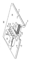
例えば図1に、集積回路120と熱コンジット140を有するプリント回路板アセンブリ100の簡略図を示す。プリント回路板または回路基板105は、第1の材料すなわち導電材料の層115に接合された電気絶縁材料の層110を含む。この例では、導電材料層115は一般に、回路基板105上の構成要素の端子の間で所望の電気的接続を行うためのパターンで構成された、流す電流に適した厚みの銅である。導電材料層115は一般に、高い熱伝導性(低い熱インピーダンス)と高い電気伝導性(低い電気インピーダンス)を有する。導電材料層115は、回路基板105の露出面のかなりの面積を占める。
For example, FIG. 1 shows a simplified diagram of a printed
回路基板105などの回路基板は、電気絶縁材料層110の上下両面上に、さらには複数の電気絶縁材料層110の間にも導電材料を有するのが一般的である。図1の例における回路基板105は、その例が不必要な詳細で不明瞭にならないように、電気絶縁材料層110の1つの面上にのみ導電材料層115を有する。図1の例では、集積回路120の電気端子すなわち端子125と1つまたは複数の端子130が、回路基板105内の開口部を挿通して、反対側の面の導電材料層115に電気的に接続している。
A circuit board such as the
示されている例では、熱コンジット140が第1の部分140Aと第2の部分140Bを含むことに留意されたい。第2の部分140Bは、実質的に回路基板105の面の平面に沿って延び、一方、第1の部分140Aは、回路基板105の面の平面とは異なる平面に沿って延びている。示されている例では、第1の部分140Aは、回路基板105の面の平面と実質的に直角の平面に沿って延びている。第1の部分140Aは、回路基板105内に形成された開口部135を通る端子に熱的に結合された第1の面142を有し、第2の部分140Bの第2の面144のかなりの部分が、導電材料層115と熱接触している。
Note that in the example shown,
この例では、集積回路120は、端子130が同電位に結合された状態で動作するように設計されている。端子130と熱コンジット140は、回路基板105内の開口部135を挿通している。端子130と導電材料層115は、熱コンジット140に、はんだまたは他の適切なボンディング材の薄層145で結合されている。
In this example, integrated
図2に、本発明の教示による例の回路基板アセンブリ200の断面をより詳細に示す。本発明の重要な特徴を強調するために、いくつかの寸法が誇張されている。電気絶縁材料層110と導電材料層115は、例えば集積回路220などの電気部品に機械的支持と電気的接続を与える回路基板205に含まれる。
FIG. 2 illustrates in greater detail a cross section of an example
集積回路220は、図2に見られる端子225、230を有する。この例では、端子225は、導電材料層115に、はんだまたは他の適切なボンディング材145によって電気的かつ熱的に結合される。端子225と導電材料層115の結合は、集積回路220を動作させるのに十分な低い電気インピーダンスをもたらすが、端子225における結合部の熱インピーダンスは、所望の熱インピーダンスよりもずっと高い。この熱インピーダンスを低減させることにより、より多くの熱が、集積回路220から端子225を経由して導電材料層115まで流れて、回路基板アセンブリ200から伝導、対流または輻射によって取り除かれる。
電気部品の端子とプリント回路板上の導電材料との間の熱インピーダンスをはんだ結合で低減させる効果的な方法が、本発明の教示による熱コンジットを使用することである。図2は、端子230と導電材料層115との間にはんだ145によって結合された熱コンジット140を示す。熱コンジット140により、はんだ145は、端子225における結合部よりもずっと広い面積にわたって端子230を導電材料層115に結合することができる。様々な例で熱コンジット140は、適切なはんだ接合を可能にするために適切な面処理またはめっきを施した、例えば銅、アルミニウム、黄銅、または鋼のうちの少なくとも1つまたは複数などの高い熱伝導性を有する材料とすることができる。様々な例でボンディング材は、導電性エポキシとすることもできる。
An effective way to reduce the thermal impedance between the electrical component terminals and the conductive material on the printed circuit board with solder bonding is to use a thermal conduit according to the teachings of the present invention. FIG. 2 shows a
図3は、本発明の教示による、熱インピーダンスをさらに低減させるために熱コンジット340を使用している例の回路基板アセンブリ300の断面を示す。図示の例に示されているように、熱コンジット340は、電気絶縁材料層110の面から上方に延び出している、すなわち集積回路220の端子230の上方に高さHv分だけ突出する。熱コンジット340の延出部360は、それが導電材料層115にはんだ145で結合されていなくても、集積回路220の端子230からの熱インピーダンスを低減させる。熱コンジット340の材料は高い熱伝導性を有するので、端子230からはんだ145を経由して熱コンジット340まで通過したいくらかの熱が、延出部360の材料にまで伝導され、そこでその熱は、延出部360の面から対流または輻射によって取り除かれる。
FIG. 3 illustrates a cross-section of an example
一例では、構成要素の回路基板への自動組立てに適用できるように、熱コンジットは実際には、それがはんだ付けされる前に回路基板上の適所にそれを保持するための機構をその構造内に含んでいる。図4は、取付タブ450を有する単一の熱伝導材料片440で形成された熱コンジット400の一例を示す。一例では、構成要素を回路基板に取り付るとき、はんだ付け作業の前や間に熱コンジット400を適所に保持させるために、取付タブ450を開口部を通過させる。
In one example, a thermal conduit actually has a mechanism in its structure to hold it in place on the circuit board before it is soldered, so that it can be applied to automatic assembly of components to the circuit board. Is included. FIG. 4 shows an example of a
さらに詳細に説明すると、図5は、1例の回路基板アセンブリ500の詳細であり、電気絶縁材料層110と導電材料層115を含む回路基板内の開口部460を通過するタブ構造すなわち取付タブ450を備えるように形成された熱伝導材料440の一部を示す。示されている例では、1つまたは複数の取付タブ450により、はんだ付けの前や間に、熱コンジット400を、他の構成要素と共に回路基板上の適所に適切な姿勢で取り付けるかまたは保持することができる。
More specifically, FIG. 5 is a detail of an example
したがって、前述のように、方法は、高い電気・熱伝導性を有する熱コンジットを準備すること、および、その熱コンジットを集積回路の1つまたは複数の電気端子に熱的に結合させることを含む。この方法は、熱コンジットを導電材料層などの第1の材料に結合させて、集積回路と回路基板の銅クラッドまたは導電材料との間の熱インピーダンスを低下させることをさらに含む。 Thus, as described above, the method includes providing a thermal conduit having high electrical and thermal conductivity and thermally coupling the thermal conduit to one or more electrical terminals of the integrated circuit. . The method further includes coupling a thermal conduit to a first material, such as a conductive material layer, to reduce the thermal impedance between the integrated circuit and the copper cladding or conductive material of the circuit board.
前述の詳細説明では、本発明の方法と装置について、その特定の例示的な実施形態を参照しながら説明してきた。しかし、本発明のより広い趣旨と範囲から逸脱することなく、本発明に様々な変更や修正が加えられうることが明らかになるであろう。したがって、本明細書と図は、限定的なものではなく例示的なものと見なされるべきである。 In the foregoing detailed description, the method and apparatus of the present invention have been described with reference to specific exemplary embodiments thereof. However, it will be apparent that various changes and modifications can be made to the invention without departing from the broader spirit and scope of the invention. The specification and drawings are accordingly to be regarded in an illustrative rather than restrictive sense.
特許請求の範囲において使用される用語は、本発明を、本明細書および特許請求の範囲で開示される特定の実施形態に限定するように解釈されるべきでない。むしろ、本発明の範囲は、クレーム解釈の確立した原則に従って解釈されるべき特許請求の範囲によって完全に決定されるべきである。 The terms used in the following claims should not be construed to limit the invention to the specific embodiments disclosed in the specification and the claims. Rather, the scope of the present invention should be determined entirely by the claims that are to be construed in accordance with established principles of claim interpretation.
100 プリント回路板アセンブリ、105 プリント回路板、回路基板、110 電気絶縁材料層、115 導電材料層、120 集積回路、125 電気端子、130 端子、135 開口部、140 熱コンジット、140A 第1の部分、140B 第2の部分、142 第1の面、144 第2の面、145 ボンディング材、200 回路基板アセンブリ、205 回路基板、220 集積回路、225 端子、230 端子、300 回路基板アセンブリ、340 熱コンジット、360 延出部、400 熱コンジット、440 熱伝導材料片、450 取付タブ、460 開口部、500 回路基板アセンブリ 100 printed circuit board assembly, 105 printed circuit board, circuit board, 110 electrically insulating material layer, 115 electrically conductive material layer, 120 integrated circuit, 125 electrical terminal, 130 terminal, 135 opening, 140 thermal conduit, 140A first part, 140B second part, 142 first surface, 144 second surface, 145 bonding material, 200 circuit board assembly, 205 circuit board, 205 integrated circuit, 225 terminal, 230 terminal, 300 circuit board assembly, 340 thermal conduit, 360 Extension, 400 Thermal Conduit, 440 Thermal Conductive Material Piece, 450 Mounting Tab, 460 Opening, 500 Circuit Board Assembly
Claims (18)
開口部、第1の面、および第2の面を含む回路基板を備え、前記開口部は前記回路基板を通って前記第1の面から前記第2の面まで延び、前記電子回路アセンブリはさらに、
前記回路基板上に取り付けられた1つまたは複数の電気端子を有する電気部品と、
第1の部分および第2の部分を有する熱コンジットとを備え、前記第1の部分は、前記開口部を通って前記電気部品の前記1つまたは複数の電気端子に熱的に結合され、前記第2の部分は、前記回路基板の第1の材料に熱的に結合され、
前記熱コンジットの前記第1と第2の部分が、それぞれ第1と第2の面を含み、前記第1の部分の前記第1の面が、前記電気部品の前記1つまたは複数の電気端子に熱的に結合され、前記第2の部分の前記第2の面のかなりの部分が、前記回路基板の前記第1の材料と熱的に接触するとともに電気的に接触し、前記熱コンジットの前記第1の部分の前記第1の面は、前記熱コンジットの前記第2の部分の前記第2の面よりも小さく、
前記電子回路アセンブリはさらに、
前記開口部内に、かつ前記熱コンジットの前記第1の部分と前記1つまたは複数の電気端子との間に配置されるボンディング材を備え、前記ボンディング材は、少なくとも前記回路基板の前記第1の面から前記回路基板の前記第2の面まで、前記熱コンジットの前記第1の部分に当接する、電子回路アセンブリ。 An electronic circuit assembly,
A circuit board including an opening, a first surface, and a second surface, the opening extending through the circuit board from the first surface to the second surface, the electronic circuit assembly further comprising: ,
An electrical component having one or more electrical terminals mounted on the circuit board;
A thermal conduit having a first portion and a second portion, wherein the first portion is thermally coupled to the one or more electrical terminals of the electrical component through the opening, A second portion is thermally coupled to the first material of the circuit board;
The first and second portions of the thermal conduit include first and second surfaces, respectively, and the first surface of the first portion is the one or more electrical terminals of the electrical component. A substantial portion of the second surface of the second portion is in thermal and electrical contact with the first material of the circuit board, and The first surface of the first portion is smaller than the second surface of the second portion of the thermal conduit;
The electronic circuit assembly further includes
A bonding material disposed in the opening and between the first portion of the thermal conduit and the one or more electrical terminals, the bonding material comprising at least the first of the circuit board; An electronic circuit assembly that abuts the first portion of the thermal conduit from a surface to the second surface of the circuit board.
開口部、第1の面、および第2の面を含む回路基板を備え、前記開口部は前記回路基板を通って前記第1の面から前記第2の面まで延び、前記電子回路アセンブリはさらに、
前記開口部を通る電気端子を含む電気部品と、
前記熱コンジットの第1の部分の第1の面および前記熱コンジットの第2の部分の第2の面を含む熱コンジットとを備え、前記第1の部分の前記第1の面は、前記電気部品の前記電気端子に熱的に結合され、前記第2の部分の前記第2の面は、前記回路基板の第1の材料に熱的に結合され、前記熱コンジットの前記第1と第2の部分が、それぞれ第1と第2の面を含み、前記第1の部分の前記第1の面が、前記電気部品の前記1つまたは複数の電気端子に熱的に結合され、前記第2の部分の前記第2の面のかなりの部分が、前記回路基板の前記第1の材料と熱的に接触するとともに電気的に接触し、前記熱コンジットの前記第1の部分の前記第1の面は、前記熱コンジットの前記第2の部分の前記第2の面よりも小さく、
前記電子回路アセンブリはさらに、
前記開口部内に、かつ前記熱コンジットの前記第1の部分の前記第1の面と前記電気端子との間に配置されるボンディング材を備え、前記ボンディング材は、少なくとも前記回路基板の前記第1の面から前記回路基板の前記第2の面まで、前記熱コンジットの前記第1の部分の前記第1の面に当接する、電子回路アセンブリ。 An electronic circuit assembly,
A circuit board including an opening, a first surface, and a second surface, the opening extending through the circuit board from the first surface to the second surface, the electronic circuit assembly further comprising: ,
An electrical component including an electrical terminal passing through the opening;
A thermal conduit including a first surface of the first portion of the thermal conduit and a second surface of the second portion of the thermal conduit, the first surface of the first portion comprising the electrical surface Thermally coupled to the electrical terminal of a component, the second surface of the second portion is thermally coupled to a first material of the circuit board, and the first and second of the thermal conduit Each of which includes first and second surfaces, wherein the first surface of the first portion is thermally coupled to the one or more electrical terminals of the electrical component, the second A substantial portion of the second surface of the portion of the first portion of the thermal conduit is in thermal and electrical contact with the first material of the circuit board and the first portion of the first portion of the thermal conduit. A surface is smaller than the second surface of the second portion of the thermal conduit;
The electronic circuit assembly further includes
A bonding material disposed in the opening and between the first surface of the first portion of the thermal conduit and the electrical terminal, wherein the bonding material is at least the first of the circuit board; An electronic circuit assembly in contact with the first surface of the first portion of the thermal conduit from the surface of the circuit board to the second surface of the circuit board.
前記熱コンジットを、回路基板上に含まれる集積回路の1つまたは複数の電気端子に熱的に結合させるステップとを備え、前記1つまたは複数の電気端子は前記回路基板内に含まれる開口を挿通し、前記開口部は前記回路基板を通って前記回路基板の第1の面から第2の面まで延び、前記熱コンジットを前記1つまたは複数の電気端子に熱的に結合させる前記ステップは、ボンディング材が、前記回路基板の前記第1の面から前記回路基板の前記第2の面まで前記熱コンジットに当接するように、前記開口部内に、かつ前記熱コンジットと前記1つまたは複数の電気端子との間に前記ボンディング材を配置するステップを含み、さらに、
前記熱コンジットを前記回路基板内に含まれる第1の材料に熱的に結合させて、前記集積回路と前記回路基板内に含まれる前記第1の材料との間の熱インピーダンスを低下させるステップとを備え、前記熱コンジットの前記第1と第2の部分が、それぞれ第1と第2の面を含み、前記第1の部分の前記第1の面が、前記電気部品の前記1つまたは複数の電気端子に熱的に結合され、前記第2の部分の前記第2の面のかなりの部分が、前記回路基板の前記第1の材料と熱的に接触するとともに電気的に接触し、前記熱コンジットの前記第1の部分の前記第1の面は、前記熱コンジットの前記第2の部分の前記第2の面よりも小さい、方法。 Providing a thermal conduit having high electrical and thermal conductivity;
Thermally coupling the thermal conduit to one or more electrical terminals of an integrated circuit included on the circuit board, wherein the one or more electrical terminals open an opening included in the circuit board. The opening extends through the circuit board from a first surface to a second surface of the circuit board, and the step of thermally coupling the thermal conduit to the one or more electrical terminals comprises: The bonding material is in the opening and the thermal conduit and the one or more so that the bonding material contacts the thermal conduit from the first surface of the circuit board to the second surface of the circuit board. Placing the bonding material between the electrical terminals, and
Thermally coupling the thermal conduit to a first material contained within the circuit board to reduce a thermal impedance between the integrated circuit and the first material contained within the circuit board; And wherein the first and second portions of the thermal conduit include first and second surfaces, respectively, and the first surface of the first portion is the one or more of the electrical components. A substantial portion of the second surface of the second portion is in thermal and electrical contact with the first material of the circuit board; and The method wherein the first surface of the first portion of the thermal conduit is smaller than the second surface of the second portion of the thermal conduit .
Applications Claiming Priority (2)
| Application Number | Priority Date | Filing Date | Title |
|---|---|---|---|
| US11/490,996 | 2006-07-20 | ||
| US11/490,996 US7593235B2 (en) | 2006-07-20 | 2006-07-20 | Thermal conduit |
Publications (3)
| Publication Number | Publication Date |
|---|---|
| JP2008060551A JP2008060551A (en) | 2008-03-13 |
| JP2008060551A5 JP2008060551A5 (en) | 2010-09-02 |
| JP5240982B2 true JP5240982B2 (en) | 2013-07-17 |
Family
ID=38457992
Family Applications (1)
| Application Number | Title | Priority Date | Filing Date |
|---|---|---|---|
| JP2007189219A Expired - Fee Related JP5240982B2 (en) | 2006-07-20 | 2007-07-20 | Heat conduit |
Country Status (4)
| Country | Link |
|---|---|
| US (1) | US7593235B2 (en) |
| EP (1) | EP1881529A3 (en) |
| JP (1) | JP5240982B2 (en) |
| CN (1) | CN101111144B (en) |
Families Citing this family (8)
| Publication number | Priority date | Publication date | Assignee | Title |
|---|---|---|---|---|
| US7817434B2 (en) * | 2004-10-14 | 2010-10-19 | Agere Systems Inc. | Method and apparatus for improving thermal energy dissipation in a direct-chip-attach coupling configuration of an integrated circuit and a circuit board |
| WO2010065113A1 (en) * | 2008-12-03 | 2010-06-10 | Planarmag,Inc. | An integrated planar variable transformer with embedded magnetic core |
| EP2276329A1 (en) * | 2009-07-16 | 2011-01-19 | ABB Research Ltd. | Electronic circuit board with a thermal capacitor |
| FI20125384L (en) * | 2012-04-04 | 2013-10-05 | Tellabs Oy | A system with a solder joint |
| KR101519187B1 (en) * | 2012-09-07 | 2015-05-11 | 엘지이노텍 주식회사 | The radiant heat member, the radiant heat circuit board and the heat generating device package |
| US20150014024A1 (en) * | 2013-07-12 | 2015-01-15 | Kevin Yang | Jumper Fin |
| US10314164B1 (en) * | 2017-12-21 | 2019-06-04 | Astec International Limited | Circuit board assemblies and methods of assembling circuit boards and bus bars |
| EP3633720A1 (en) * | 2018-10-05 | 2020-04-08 | Aros Electronics AB | Surface mounted heat buffer |
Family Cites Families (19)
| Publication number | Priority date | Publication date | Assignee | Title |
|---|---|---|---|---|
| GB986824A (en) * | 1962-01-02 | 1965-03-24 | Gen Electric Co Ltd | Improvements in or relating to printed electric circuits |
| US4254447A (en) * | 1979-04-10 | 1981-03-03 | Rca Corporation | Integrated circuit heat dissipator |
| JPS6369883A (en) * | 1986-09-12 | 1988-03-29 | Mitsubishi Gas Chem Co Inc | Adhesive composition having thermal and electrical conductivity |
| JPS63204689A (en) * | 1987-02-20 | 1988-08-24 | オ−ケ−プリント配線株式会社 | Hybrid substrate |
| JPH0629168U (en) * | 1992-09-18 | 1994-04-15 | 株式会社富士通ゼネラル | Soldering parts |
| JP3207293B2 (en) * | 1993-05-10 | 2001-09-10 | ダイヤセミコンシステムズ株式会社 | Pin type socket and collective type socket for mounting IC components |
| KR0126781Y1 (en) * | 1994-08-23 | 1999-05-01 | 이형도 | Radiation apparatus for semiconductor element |
| EP0706221B8 (en) * | 1994-10-07 | 2008-09-03 | Hitachi, Ltd. | Semiconductor device comprising a plurality of semiconductor elements |
| JPH1084175A (en) * | 1996-09-06 | 1998-03-31 | Canon Inc | Heat dissipation thermal conduction means of electric part |
| JPH10242614A (en) * | 1997-02-26 | 1998-09-11 | Canon Inc | Component mounting plate |
| US5920458A (en) * | 1997-05-28 | 1999-07-06 | Lucent Technologies Inc. | Enhanced cooling of a heat dissipating circuit element |
| US5896271A (en) * | 1997-07-21 | 1999-04-20 | Packard Hughes Interconnect Company | Integrated circuit with a chip on dot and a heat sink |
| US6097603A (en) * | 1997-10-22 | 2000-08-01 | Thermalloy, Incorporated | Heat sink for direct attachment to surface mount electronic device packages |
| JPH11195889A (en) * | 1997-12-27 | 1999-07-21 | Nec Home Electron Ltd | Heat radiating part for printed board |
| JP2001135906A (en) * | 1999-11-05 | 2001-05-18 | Yazaki Corp | Electric component connection structure of wiring board |
| US7183640B2 (en) * | 1999-12-13 | 2007-02-27 | Lamina Ceramics, Inc. | Method and structures for enhanced temperature control of high power components on multilayer LTCC and LTCC-M boards |
| US6351385B1 (en) * | 2000-09-26 | 2002-02-26 | Thomson Licensing, S.A. | Heat sink for integrated circuit packages |
| JP2004253759A (en) * | 2002-12-24 | 2004-09-09 | Auto Network Gijutsu Kenkyusho:Kk | Control circuit board and circuit construct |
| JP4155048B2 (en) * | 2003-02-14 | 2008-09-24 | 住友電装株式会社 | Power module and manufacturing method thereof |
-
2006
- 2006-07-20 US US11/490,996 patent/US7593235B2/en not_active Expired - Fee Related
-
2007
- 2007-07-19 EP EP07252857A patent/EP1881529A3/en not_active Withdrawn
- 2007-07-20 JP JP2007189219A patent/JP5240982B2/en not_active Expired - Fee Related
- 2007-07-20 CN CN2007101464785A patent/CN101111144B/en not_active Expired - Fee Related
Also Published As
| Publication number | Publication date |
|---|---|
| JP2008060551A (en) | 2008-03-13 |
| EP1881529A3 (en) | 2010-09-22 |
| CN101111144A (en) | 2008-01-23 |
| US7593235B2 (en) | 2009-09-22 |
| CN101111144B (en) | 2012-06-20 |
| US20080017406A1 (en) | 2008-01-24 |
| EP1881529A2 (en) | 2008-01-23 |
Similar Documents
| Publication | Publication Date | Title |
|---|---|---|
| JP5240982B2 (en) | Heat conduit | |
| KR102332362B1 (en) | Ultra-thin embedded semiconductor device package and method of manufacturing therof | |
| JP5106519B2 (en) | Thermally conductive substrate and electronic component mounting method thereof | |
| KR19990062684A (en) | Integrated circuit package and how to connect it to the substrate | |
| JPH10229147A (en) | Connection of cantilever ball for integrated circuit chip package | |
| JP2009105036A (en) | Terminal mounting structure, and terminal mounting method | |
| US20180326924A1 (en) | Circuit assembly and electrical junction box | |
| US7709744B2 (en) | Gas venting component mounting pad | |
| EP1345265A2 (en) | Electronics assembly with improved heatsink configuration | |
| JP2008060551A5 (en) | ||
| JP2009230897A (en) | Electronic component jointing device, electronic unit, and electronic device | |
| JP2008141027A (en) | Bonding structure of thermoelectric conversion element and thermoelectric conversion module | |
| JP2009176996A (en) | High frequency circuit board | |
| US6858807B2 (en) | Substrate for receiving a circuit configuration and method for producing the substrate | |
| JP2007227452A (en) | Flexible wiring board, its solder bonding method and optical transmitting package using the same | |
| GB2345576A (en) | Heat-sink of ICs and method of mounting to PCBs | |
| JP2013165207A (en) | Circuit board with conductor and manufacturing method therefor | |
| JP5024009B2 (en) | Electronic circuit mounting method and mounting structure | |
| JP2007194160A (en) | Printed circuit board connecting method | |
| TWI796707B (en) | Method for printed circuit board (pcb) ground and pcb and circuit using the same | |
| JP2009238926A (en) | Tab tape and method of manufacturing the same | |
| JP4770504B2 (en) | Printed circuit board and printed circuit board manufacturing method | |
| JP2001223452A (en) | Circuit board | |
| JP2001217101A (en) | Resistor for detecting current | |
| JPH08191128A (en) | Electronic device |
Legal Events
| Date | Code | Title | Description |
|---|---|---|---|
| RD03 | Notification of appointment of power of attorney |
Free format text: JAPANESE INTERMEDIATE CODE: A7423 Effective date: 20090310 |
|
| A521 | Written amendment |
Free format text: JAPANESE INTERMEDIATE CODE: A821 Effective date: 20090501 |
|
| RD04 | Notification of resignation of power of attorney |
Free format text: JAPANESE INTERMEDIATE CODE: A7424 Effective date: 20090501 |
|
| A521 | Written amendment |
Free format text: JAPANESE INTERMEDIATE CODE: A523 Effective date: 20100716 |
|
| A621 | Written request for application examination |
Free format text: JAPANESE INTERMEDIATE CODE: A621 Effective date: 20100716 |
|
| A131 | Notification of reasons for refusal |
Free format text: JAPANESE INTERMEDIATE CODE: A131 Effective date: 20120612 |
|
| A521 | Written amendment |
Free format text: JAPANESE INTERMEDIATE CODE: A523 Effective date: 20120830 |
|
| TRDD | Decision of grant or rejection written | ||
| A01 | Written decision to grant a patent or to grant a registration (utility model) |
Free format text: JAPANESE INTERMEDIATE CODE: A01 Effective date: 20130305 |
|
| A61 | First payment of annual fees (during grant procedure) |
Free format text: JAPANESE INTERMEDIATE CODE: A61 Effective date: 20130401 |
|
| FPAY | Renewal fee payment (event date is renewal date of database) |
Free format text: PAYMENT UNTIL: 20160412 Year of fee payment: 3 |
|
| R150 | Certificate of patent or registration of utility model |
Free format text: JAPANESE INTERMEDIATE CODE: R150 |
|
| R250 | Receipt of annual fees |
Free format text: JAPANESE INTERMEDIATE CODE: R250 |
|
| R250 | Receipt of annual fees |
Free format text: JAPANESE INTERMEDIATE CODE: R250 |
|
| LAPS | Cancellation because of no payment of annual fees |