JP5240913B2 - Method for manufacturing container for electronic component - Google Patents
Method for manufacturing container for electronic component Download PDFInfo
- Publication number
- JP5240913B2 JP5240913B2 JP2008255705A JP2008255705A JP5240913B2 JP 5240913 B2 JP5240913 B2 JP 5240913B2 JP 2008255705 A JP2008255705 A JP 2008255705A JP 2008255705 A JP2008255705 A JP 2008255705A JP 5240913 B2 JP5240913 B2 JP 5240913B2
- Authority
- JP
- Japan
- Prior art keywords
- resist
- plating
- wafer
- main surface
- substrate
- Prior art date
- Legal status (The legal status is an assumption and is not a legal conclusion. Google has not performed a legal analysis and makes no representation as to the accuracy of the status listed.)
- Active
Links
Images


Landscapes
- Piezo-Electric Or Mechanical Vibrators, Or Delay Or Filter Circuits (AREA)
Description
本発明は、電子機器に使用される電子部品の電子部品用容器体の製造方法に関する。 The present invention relates to a process for the production of electronic components for containers of electronic components used in electronic devices.
電子機器が小型化されるにつれ、電子部品も小型化されている。その電子部品は、振動および衝撃に耐えうるように平面全体で支持する表面実装型が増加している。 As electronic devices are downsized, electronic components are also downsized. As for the electronic components, surface mount types that support the entire plane so as to withstand vibration and impact are increasing.
このような電子部品には、例えば、圧電振動子や圧電発振器などがある。ここで、従来の圧電振動子について説明する。従来の圧電振動子は、電子部品用容器体と圧電振動素子と蓋とから主に構成されている。この圧電振動子の構造は、圧電振動素子を電子部品用容器体と蓋とで完全に包囲した状態で、封止された構造となっている。 Examples of such electronic components include a piezoelectric vibrator and a piezoelectric oscillator. Here, a conventional piezoelectric vibrator will be described. Conventional piezoelectric vibrators are mainly composed of a container body for electronic parts, a piezoelectric vibration element, and a lid. The structure of the piezoelectric vibrator is a sealed structure in a state in which the piezoelectric vibration element is completely surrounded by the electronic component container and the lid.
電子部品用容器体は、一方の主面に凹部を有し、その内部に圧電振動素子を電気的に接続するための接続用端子と、他方の主面に外部接続端子とを備えている。また、前記接続用端子と前記外部接続端子とが電気的に接続された構造となっている。 The container body for electronic components has a recess on one main surface, and includes a connection terminal for electrically connecting the piezoelectric vibration element therein and an external connection terminal on the other main surface. Further, the connection terminal and the external connection terminal are electrically connected.
また、電子部品用容器体は、セラミック、樹脂、水晶、ガラス、シリコンなどの絶縁材料から主に構成されている。 Moreover, the container body for electronic components is mainly comprised from insulating materials, such as a ceramic, resin, quartz crystal, glass, and silicon.
ここで、電子部品用容器体がセラミックから主に構成されている場合について説明する。
電子部品用容器体は、所定の位置に2つ一対の貫通孔を有した基板部と、基板部の一方の主面に圧電素子と電気的に接続させるための接続用端子と、基板部の一方の主面の周囲に設けられた壁部と、基板部の一方の主面と平行となる壁部の面に設けられた蓋を接合するための金属層と、基板部の他方の主面に複数設けられた外部接続端子とから構成されている。また、基板部の他方の主面に複数設けられている外部接続端子の2つは、前記貫通孔を介して接続用端子と電気的に接続される構造となっている(例えば特許文献1参照)。
Here, the case where the container body for electronic components is mainly comprised from the ceramic is demonstrated.
The electronic component container includes a substrate portion having two pairs of through holes at predetermined positions, a connection terminal for electrically connecting the piezoelectric element to one main surface of the substrate portion, A wall provided around one main surface, a metal layer for bonding a lid provided on the surface of the wall parallel to one main surface of the substrate portion, and the other main surface of the substrate portion And a plurality of external connection terminals. Further, two of the external connection terminals provided on the other main surface of the substrate portion are electrically connected to the connection terminals via the through holes (see, for example, Patent Document 1). ).
電子部品用容器体が、水晶、ガラス、シリコンのいずれか一つから選択された材料で主に構成されている場合について説明する。
電子部品用容器体は、基板部と壁部と接続用端子と外部接続端子とから構成されている。接続用端子は、基板部の一方の主面に形成されており、圧電振動素子と電気的に接続される。外部接続端子は、基板の他方の主面に複数設けられている。壁部は、基板の一方の主面の周囲に設けられている(例えば特許文献2参照)。
The container for electronic parts is comprised from the board | substrate part, the wall part, the terminal for a connection, and the external connection terminal. The connection terminal is formed on one main surface of the substrate portion and is electrically connected to the piezoelectric vibration element. A plurality of external connection terminals are provided on the other main surface of the substrate. The wall portion is provided around one main surface of the substrate (see, for example, Patent Document 2).
しかしながら、小型化・薄型化に伴い次の様な問題があった。
電子部品容器体をセラミックで形成する場合、焼成によって収縮するため焼成前と焼成後では、寸法にばらつきが生じてしまう。そのため、セラミックから主に構成される電子部品用容器体は、水晶、ガラス、シリコン、樹脂などのいずれか一つから選択された材料からなる電子部品用容器体と比較して、外形の寸法精度が悪くなる。焼成の際に収縮するため、水晶、ガラス、シリコンや樹脂などのいずれか一つから選択された材料で主に構成されている電子部品用容器体の外形寸法精度と比較して、外形寸法が悪くなる。
電子部品用容器体の外形の寸法精度が悪い場合、電子部品用容器体の外形寸法と蓋の外形寸法にずれが生じる。そのため、電子部品用容器体の壁部と蓋の重なる面積が小さくなり、封止が完全になされなくなる。従って、セラミックからなる電子部品用容器体を用いた圧電振動子は、外部の温度や湿度の影響を受けやすくなり、圧電振動子の電気的特性の悪化や、圧電振動子の周波数の安定度を悪化させることがあった。
However, there have been the following problems with downsizing and thinning.
In the case where the electronic component container body is formed of ceramic, the size shrinks before and after firing because of shrinkage due to firing. For this reason, the container body for electronic components mainly composed of ceramic is more accurate than the container body for electronic components made of a material selected from any one of quartz, glass, silicon, resin, etc. Becomes worse. Because it shrinks during firing, its outer dimensions are smaller than the outer dimension accuracy of the container body for electronic components mainly composed of a material selected from any one of quartz, glass, silicon, resin, etc. Deteriorate.
When the dimensional accuracy of the outer shape of the electronic component container is poor, the outer size of the electronic component container and the outer size of the lid are shifted. Therefore, the area where the wall portion of the electronic component container and the lid overlap is reduced, and the sealing is not completed completely. Therefore, a piezoelectric vibrator using a ceramic container body for electronic components is easily affected by external temperature and humidity, and the electrical characteristics of the piezoelectric vibrator are deteriorated and the frequency stability of the piezoelectric vibrator is reduced. It sometimes made it worse.
水晶、ガラス、シリコンのいずれか一つから選択された材料から構成されている電子部品用容器体を用いた場合には、次の問題があった。
水晶、ガラス、シリコン、その他圧電材料のいずれか一つから選択された材料から主に構成されている電子部品用容器体は、非金属からなる基板部と基板部と同一の材料からなる壁部とから構成されている。この電子部品用容器体を用いて圧電振動子に用いた場合、圧電振動素子は、絶縁材料で完全に包囲される。そのため圧電振動子は、外部の電磁波等のノイズを防ぐことができない。
このため、水晶、ガラス、シリコン、その他圧電材料のいずれか一つから選択した材料から構成されている電子部品用容器体を用いた圧電振動子は、セラミックから構成される電子部品用容器体を用いた圧電振動子と比較して、圧電振動子の電気的特性の悪化や、圧電振動子の周波数の安定度の悪化という問題があった。
In the case of using a container for electronic parts made of a material selected from any one of quartz, glass, and silicon, there are the following problems.
A container body for electronic parts mainly composed of a material selected from any one of quartz, glass, silicon, and other piezoelectric materials is a non-metal substrate portion and a wall portion made of the same material as the substrate portion. It consists of and. When this electronic component container is used for a piezoelectric vibrator, the piezoelectric vibration element is completely surrounded by an insulating material. Therefore, the piezoelectric vibrator cannot prevent noise such as external electromagnetic waves.
For this reason, a piezoelectric vibrator using an electronic component container body made of a material selected from any one of quartz, glass, silicon, and other piezoelectric materials has an electronic component container body made of ceramic. Compared to the piezoelectric vibrator used, there were problems that the electrical characteristics of the piezoelectric vibrator deteriorated and the frequency stability of the piezoelectric vibrator deteriorated.
そこで、本発明は、前記した問題を解決し、圧電振動子の電気的特性の悪化を防ぎ、周波数を安定させる圧電振動子を可能とする、電子部品用容器体の製造方法を提供することを目的とする。 Accordingly, the present invention is to solve the above described problems, preventing deterioration of the electrical characteristics of the piezoelectric vibrator, allowing the piezoelectric vibrator to stabilize the frequency, to provide a method of manufacturing electronic components for the container body With the goal.
前記課題を解決するため、本発明は、圧電デバイス用容器体の製造方法であって、複数の基板となる部分が設けられ、前記基板となる部分の縁に沿って設けられるグラウンドに接続されためっき用金属層と前記めっき用金属層の内側であって2つ一対で設けられる配線パターンとを一方の主面に有し、前記基板となる部分の4隅に設けられる外部接続端子を他方の主面に有したウエハの一方の主面に、レジストを後述する壁部と同じ厚みまで付着させるレジスト付着工程と、前記めっき用金属層と重なる部分の前記レジストを除去する第一のレジスト除去工程と、電解めっき又は無電解めっきにより、前記めっき用金属層に所定の金属からなり且つ前記レジストと同じ厚みとなるめっき形成壁部を設けるめっき工程と、前記ウエハの一方の主面に付着しているレジストを全て除去する第二のレジスト除去工程と、前記めっき形成壁部の前記ウエハと平行となる面を平滑にする平滑工程と、前記ウエハを基板ごとに個片化し、各基板の一方の主面に壁部を有する電子部品用容器体を得る個片化工程と、からなることを特徴とする。 In order to solve the above-mentioned problem, the present invention is a method for manufacturing a container body for a piezoelectric device, wherein a portion to be a plurality of substrates is provided and connected to a ground provided along an edge of the portion to be the substrate. A metal layer for plating and a wiring pattern provided in pairs inside the metal layer for plating are provided on one main surface, and external connection terminals provided at four corners of the portion to be the substrate are provided on the other side. A resist attaching step for attaching a resist to one main surface of the wafer held on the main surface to the same thickness as a wall portion described later, and a first resist removing step for removing the resist in a portion overlapping with the plating metal layer When, by electrolytic plating or electroless plating, a plating step of forming a Rumekki forming wall, such as the same thickness as and the resist Ri Do from a predetermined metal to the plating metal layer, one of the main of the wafer A second resist removal step of removing all the in and resist adhering to the smoothing process of the wafer and the parallel plane of the plating wall smooth, and singulating the wafer for each substrate, each And an individualizing step for obtaining a container body for electronic parts having a wall portion on one main surface of the substrate .
また、前記課題を解決するため、本発明は、圧電デバイス用容器体の製造方法であって、複数の基板となる部分が設けられ、前記基板となる部分の縁に沿って設けられるめっき用金属層と前記めっき用金属層の内側であって2つ一対で設けられる配線パターンとを一方の主面に有し、前記基板となる部分の4隅に設けられる外部接続端子を他方の主面に有したウエハの前記一方の主面に、レジストを後述する壁部と同じ厚みまで付着させるレジスト付着工程と、前記めっき用金属層と重なる部分の前記レジストを除去する第一のレジスト除去工程と、電解めっき又は無電解めっきにより、前記めっき用金属層に所定の金属からなり且つ前記レジストと同じ厚みとなるめっき形成壁部を設けるめっき工程と、 前記ウエハの一方の主面に付着しているレジストを全て除去する第二のレジスト除去工程と、前記めっき形成壁部の前記ウエハと平行となる面を平滑にする平滑工程と、前記ウエハを基板ごとに個片化し、各基板の一方の主面に壁部を有する電子部品用容器体を得る個片化工程と、前記壁部と前記外部接続端子のうちグラウンドとなる前記外部接続端子とを電気的に接続する導電部を、前記電子部品用容器体の外側面に形成する導電部形成工程と、からなることを特徴とする。 Moreover, in order to solve the said subject, this invention is a manufacturing method of the container body for piezoelectric devices, Comprising: The metal for plating provided in the part used as the some board | substrate, and provided along the edge of the part used as the said board | substrate An external connection terminal provided at four corners of a portion to be the substrate on one main surface, and a wiring pattern provided in a pair on the inside of the metal layer for plating and two in pairs A resist adhering step for adhering a resist to the same thickness as a wall portion to be described later, and a first resist removing step for removing the resist in a portion overlapping the metal layer for plating; by electrolytic plating or electroless plating, a plating step of forming a Rumekki forming wall, such as the same thickness as and the resist Ri Do from a predetermined metal to the plating metal layer, adhered to one main surface of the wafer A second resist removing step for removing all of the resist, a smoothing step for smoothing a surface parallel to the wafer of the plating forming wall, and separating the wafer for each substrate, An electronic component container body having a wall portion on a main surface, and a conductive portion that electrically connects the wall portion and the external connection terminal serving as a ground among the external connection terminals, And a conductive part forming step formed on the outer surface of the component container .
また本発明は、レジストがドライフィルムレジストであっても良い。 In the present invention, the resist may be a dry film resist.
このような電子部品用容器体を用いた圧電振動子は、セラミックを焼成して形成する電子部品用容器体を用いた圧電振動子と比較して、電子部品用容器体の外形寸法精度がよくなるため、電子部品用容器体と蓋の重なる面積が大きくなる。このため、このような電子部品用容器体を用いた圧電振動子は、気密性を保った状態で封止されるため、外部の温度や湿度の影響による圧電振動子の電気的特性の悪化や圧電振動子の周波数の悪化を防ぐことができる。 A piezoelectric vibrator using such a container body for electronic components has better external dimension accuracy of the container body for electronic components than a piezoelectric vibrator using a container body for electronic parts formed by firing ceramics. For this reason, the area where the electronic component container and the lid overlap increases. For this reason, a piezoelectric vibrator using such a container body for electronic parts is sealed in an airtight state, so that the electrical characteristics of the piezoelectric vibrator are deteriorated due to the influence of external temperature and humidity. Deterioration of the frequency of the piezoelectric vibrator can be prevented.
さらに、このような電子部品用容器体を使用した圧電振動子は、水晶、ガラス、シリコンのいずれか一つから選択された材料から主に構成された電子部品用容器体を使用した圧電振動子と比較して、圧電振動子の電気的特性の悪化や圧電振動子の周波数の悪化を防ぐことができる。このような電子部品用容器体を使用した圧電振動子は、壁部が金属から構成されているので、電磁波等の外部のノイズによる影響を防ぐことができる。このとき、金属から構成される蓋を用いることで、さらに外部のノイズによる影響を防ぐことができる。 Furthermore, the piezoelectric vibrator using such a container body for electronic parts is a piezoelectric vibrator using a container body for electronic parts mainly composed of a material selected from any one of quartz, glass, and silicon. As compared with the above, it is possible to prevent the deterioration of the electrical characteristics of the piezoelectric vibrator and the deterioration of the frequency of the piezoelectric vibrator. In the piezoelectric vibrator using such a container for electronic parts, the wall portion is made of metal, so that the influence of external noise such as electromagnetic waves can be prevented. At this time, the use of a lid made of metal can further prevent the influence of external noise.
このような圧電振動子の構造は、壁部と外部接続端子の所定の一つを介してグラウンドに電気的に接続する構造となっている。そのため、このような電子部品用容器体を用いた圧電振動子は、壁部で発生した浮遊容量をグラウンドに放出でき、浮遊容量による圧電振動子の電気的特性の悪化や圧電振動子の周波数の安定度の悪化を防ぐことができる。 Such a piezoelectric vibrator has a structure in which the piezoelectric vibrator is electrically connected to the ground via a predetermined one of the wall portion and the external connection terminal. For this reason, a piezoelectric vibrator using such a container for electronic components can discharge stray capacitance generated at the wall portion to the ground. Deterioration of stability can be prevented.
従って、このような電子部品用容器体を用いることによって、圧電振動子の電気的特性の悪化を防ぎ、圧電振動子の周波数の安定している圧電振動子を得ることができる。 Therefore, by using such a container for electronic components, it is possible to prevent deterioration of the electrical characteristics of the piezoelectric vibrator and obtain a piezoelectric vibrator having a stable frequency of the piezoelectric vibrator.
本発明の製造方法は、めっき形成壁部を形成する際にめっき法を用いる。めっき法を用いた場合は、めっき形成壁部の形成にスパッタまたは蒸着を用いた場合と比較して、壁部の外形寸法が良くなる。また、リードタイムも短縮できるため、生産コストも安くなる。 The manufacturing method of the present invention uses a plating method when forming the plating forming wall. When the plating method is used, the outer dimension of the wall portion is improved as compared with the case where sputtering or vapor deposition is used to form the plating formation wall portion. In addition, since the lead time can be shortened, the production cost is also reduced.
このように本発明の製造方法を用いることにより、壁部の外形寸法精度がよく、生産コストの安い電子部品用容器体を製造することができる。 As described above, by using the manufacturing method of the present invention, it is possible to manufacture a container body for an electronic component having a good external dimension accuracy of the wall portion and a low production cost.
次に、本発明を実施するための最良の形態(以下、「実施形態」という。)について、適宜図面を参照しながら詳細に説明する。また、各構成要素について状態をわかりやすくするために誇張して図示している。 Next, the best mode for carrying out the present invention (hereinafter referred to as “embodiment”) will be described in detail with reference to the drawings as appropriate. In addition, each component is exaggerated for easy understanding of the state.
(第一の実施形態)
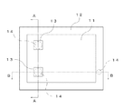
図1は、本発明の第一の実施形態に係る電子部品用容器体の斜視図である。図2は、本発明の第一の実施形態に係る電子部品用容器体を基板部の一方の主面から見た場合の概念図である。図3は、本発明の第一の実施形態に係る電子部品用容器体を基板部の他方の主面から見た場合の概念図である。図4は、図2のA−A断面の概念図である。図5は、図2のB−B断面の概念図である。
(First embodiment)
FIG. 1 is a perspective view of a container body for an electronic component according to the first embodiment of the present invention. FIG. 2 is a conceptual diagram when the electronic component container according to the first embodiment of the present invention is viewed from one main surface of the substrate portion. FIG. 3 is a conceptual diagram when the electronic component container according to the first embodiment of the present invention is viewed from the other main surface of the substrate portion. FIG. 4 is a conceptual diagram of the AA cross section of FIG. FIG. 5 is a conceptual diagram of the BB cross section of FIG.
本発明の実施形態に係る電子部品用容器体は、基板部11と壁部12と配線パターン13と外部接続端子15とから主に構成される。
The electronic component container according to the embodiment of the present invention is mainly composed of a substrate portion 11, a
基板部11は、水晶、ガラス、シリコン、焼成後のセラミックのいずれか一つから選択され複数のスルーホール14を有している。基板部11の板厚は、圧電振動子として強度が保てる板厚となっている。
ここで、基板部11が水晶からなる場合について説明する。
水晶からなる基板部11を用いた電子部品用容器体は、セラミックから主に構成された電子部品用容器体と比較して、焼成による伸縮がないため外形寸法精度がよい。そのため、この電子部品用容器体を用いた圧電振動子は、気密性の高い状態で封止され、圧電振動子の特性の悪化および圧電振動子の周波数の安定度の悪化を防ぐことができる。
The substrate portion 11 has a plurality of through
Here, the case where the board | substrate part 11 consists of quartz is demonstrated.
The electronic component container body using the substrate portion 11 made of quartz has better dimensional accuracy because there is no expansion and contraction due to firing, compared to an electronic component container body mainly composed of ceramic. Therefore, the piezoelectric vibrator using the container for electronic parts is sealed in a highly airtight state, and deterioration of the characteristics of the piezoelectric vibrator and deterioration of the frequency stability of the piezoelectric vibrator can be prevented.
配線パターン13は、前記基板部11の一方の主面に後述する壁部12より内側に位置し2つ一対で設けられる。配線パターン13は、フォトリソグラフィ技術とエッチング技術により形成されている。また、配線パターン13は、圧電振動素子との電気的に接続させる接続用端子に相当している。配線パターン13は、圧電振動素子を電子部品容器体に表面実装する際に、圧電振動素子の電気的信号の取り出しパターンに合わせて電子部品用容器体内に配置されている。
The
外部接続端子15は、前記基板部11の他方の主面に複数設けられている。外部接続端子15の所定の1つは、後述する壁部12と前記貫通孔14を介して電気的に接続しつつグラウンドと接続されている。また、外部接続端子15の所定の他の2つは、前記他の貫通孔14を介して前記配線パターン13と電気的に接続されている。外部接続端子15は、フォトリソグラフィ技術とエッチング技術を用いて、前記基板部11の他方の主面の4隅に形成されている。
A plurality of
壁部12は、金属からなり、基板部11の一方の主面の縁にそって形成されている金属層12M上に枠状に形成されている。壁部12の高さは、圧電振動素子を基板部11と壁部12と蓋(図示せず)で完全に包囲できる高さとなっている。例えば、壁部12の高さは、0.1〜0.3mmとなっている。壁部12の幅は、電子部品用容器体として強度が保てる幅となっている。
The
また、この電子部品用容器体は、金属からなる壁部12と金属層12Mとが用いられているので、電磁波等の外部のノイズの影響を回避することができる。このため、この電子部品用容器体を使用した圧電振動子は、電磁波等の外部のノイズの影響による圧電振動子の電気的特性の悪化および圧電振動子の周波数の安定度の悪化を防ぐことができる。
壁部12は、グラウンドと電気的に接続されている。つまり、壁部12は、所定の外部接続端子15とグラウンドに接続されているので、電子部品容器体自身で発生した浮遊容量による影響を回避することができる。このため、この電子部品用容器体を使用した圧電振動子は、浮遊容量による圧電振動子の電気的特性の悪化および圧電振動子の周波数の安定度の悪化を防ぐことができる。
Moreover, since the
The
この電子部品用容器体の製造方法は、壁部12が金属によって形成されているので電気的特性の悪化と周波数の安定した圧電振動子を提供することができる。
This method of manufacturing an electronic component container can provide a piezoelectric vibrator having a stable electric frequency and a stable frequency because the
次に本発明の電子部品用容器体の製造方法の実施形態について説明する。
本発明の電子部品用容器体は、レジスト付着工程と第一のレジスト除去工程とめっき工程と第二のレジスト除去工程と平滑工程と個片化工程とを経て製造されている。
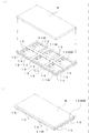
図6〜図9は、第一の実施形態の電子部品用容器体の製造工程時の部分的な形態の概念図を示したものである。
Next, an embodiment of a method for manufacturing an electronic component container according to the present invention will be described.
The electronic component container of the present invention is manufactured through a resist adhesion step, a first resist removal step, a plating step, a second resist removal step, a smoothing step, and an individualization step.
6 to 9 show conceptual diagrams of partial forms during the manufacturing process of the electronic component container according to the first embodiment.
レジスト付着工程は、複数の基板となる部分が設けられ、前記基板となる部分の縁に沿って設けられるグラウンドに接続されためっき用金属層12MWと前記めっき用金属層12MWの内側であって2つ一対で設けられる配線パターン13とを一方の主面に有し、前記基板となる部分の4隅に設けられる外部接続端子15を他方の主面に有したウエハ11Wの一方の主面にレジストRを付着させる工程である。
The resist attaching step includes a plurality of substrates to be provided, and the inside of the
まず、ウエハ11Wについて説明する。
前記ウエハ11Wは、複数の前記基板をマトリックス状に配列された状態となっている。この基板は、電子部品用容器体の基板部11に相当する。
この基板は、複数の貫通孔14を有している。この貫通孔14は、フォトリソグラフィ技術とエッチング技術等により形成される。この貫通孔14を導電ペーストで塞ぐことにより、基板の一方の主面と他方の主面とが、電気的に接続される。
前記ウエハ11Wの一方の主面には、めっき用金属層12MWがフォトリソグラフィ技術とエッチング技術により形成されている。また、このめっき用金属層12MWは、基板ごとに個片化する際の切り代分を含んでいるため、第一の実施形態に係る電子部品用容器体の壁部の厚みよりも厚くなっている。このめっき用金属層12MWは、前記ウエハ11Wの他方の主面の外部接続端子15と貫通孔14を介して電気的に接続されている。
前記ウエハ11Wの一方の主面には、配線パターン13がフォトリソグラフィ技術とエッチング技術により形成されている。この配線パターン13は、めっき用金属層12MWの内側であって2つ一対で設けられており、圧電振動素子を表面実装できるように配置されている。また、配線パターン13は、特定の貫通孔14を介して所定の外部接続端子15と電気的に接続されている。
First, the wafer 11W will be described.
The wafer 11W has a plurality of substrates arranged in a matrix. This board | substrate is corresponded to the board | substrate part 11 of the container body for electronic components.
This substrate has a plurality of through
On one main surface of the wafer 11W, a plating metal layer 12MW is formed by a photolithography technique and an etching technique. In addition, since the plating metal layer 12MW includes a cutting allowance when individualized for each substrate, it is thicker than the thickness of the wall portion of the electronic component container according to the first embodiment. Yes. The plating metal layer 12MW is electrically connected to the
A
付着させるレジストRの厚みは、例えば、電子部品用容器体の壁部12の高さと同じ厚みとする。例えば、壁部12の高さが0.1〜0.3mmの場合は、レジストRの厚みを0.1mm〜0.3mmとする。
このレジストは、ポジ型フォトレジストだけでなく、ネガ型フォトレジストを使用しても構わない。
またこのレジストは、ドライフィルムレジストのようなドライレジストだけでなく、液状のレジストを使用しても構わない。
ウエハ11Wの一方の主面にレジストRが付着されている状態のウエハを、レジスト付着工程後ウエハとする。レジスト付着工程後ウエハの概念図を図6(b)に示す。
The thickness of the resist R to be attached is, for example, the same thickness as the height of the
As this resist, not only a positive type photoresist but also a negative type photoresist may be used.
Further, as this resist, not only a dry resist such as a dry film resist but also a liquid resist may be used.
A wafer in which the resist R is attached to one main surface of the wafer 11W is referred to as a wafer after the resist attaching process. A conceptual diagram of the wafer after the resist attaching step is shown in FIG.
第一のレジスト除去工程は、前記レジストRの前記めっき用金属層12MWと重なる部分を除去する工程である。
第一のレジスト除去工程には、フォトリソグラフィ技術とエッチング技術を用いる。
レジスト付着工程後ウエハは、前記めっき用金属層12MWと重なる部分を除去できるように露光マスクを合わせた状態で、前記レジストRに合わせた一定時間露光され、その後、前記レジストRに合わせた現像液で現像される。現像されたレジスト付着工程後ウエハは、前記めっき用金属層12MWと重なっている部分のレジストRを除去される。
前記レジストRが液状のものを使用した場合には、第一のレジスト工程後に乾燥を行う。
めっき用金属層12MWと重なっている部分のレジストRのみ除去されたレジスト付着工程後のウエハを、第一のレジスト除去工程後ウエハとする。第一のレジスト除去工程後ウエハの概念図を図7に示す。
The first resist removing step is a step of removing a portion of the resist R that overlaps with the plating metal layer 12MW.
For the first resist removal step, a photolithography technique and an etching technique are used.
After the resist adhesion process, the wafer is exposed for a certain time according to the resist R in a state where an exposure mask is aligned so that a portion overlapping the metal layer for plating 12 MW can be removed, and then a developer corresponding to the resist R Developed with After the developed resist adhesion step, the portion of the resist R overlapping the plating metal layer 12MW is removed.
When the resist R is liquid, drying is performed after the first resist process.
The wafer after the resist attaching process in which only the portion of the resist R overlapping with the plating metal layer 12MW is removed is referred to as a wafer after the first resist removing process. A conceptual diagram of the wafer after the first resist removal step is shown in FIG.
めっき工程は、電解めっき又は無電解めっきにより、前記めっき用金属層12MWに所定の金属からなるめっき形成壁部12Wを設ける工程である。
めっき形成壁部12Wは、電気化学反応を利用して、露出されためっき用金属層12MW上に、所定の金属で形成される。そのめっき形成壁部12Wの厚みは、レジスト付着工程で付着させた前記レジストRの厚みと同等とする。めっき形成壁部12Wの厚みは、例えば、0.1〜0.3mmとなる。
めっき方法は、電解めっき、無電解めっきのいずれか一つの方法を使用する。
めっき形成壁部12Wを形成する金属は、特に指定しない。電磁波等のシールド効果の高い金属の使用により、圧電振動子の電気的特性の悪化を防ぎ、圧電振動子の周波数の安定度の悪化を防ぐ効果を上げることができる。めっき形成壁部12Wを構成する金属の例として、銅、ニッケルなどが挙げられる。
めっき工程後のウエハの概念図を図8に示す。
The plating step is a step of providing a plating forming wall portion 12W made of a predetermined metal on the plating metal layer 12MW by electrolytic plating or electroless plating.
The plating forming wall portion 12W is formed of a predetermined metal on the exposed plating metal layer 12MW using an electrochemical reaction. The thickness of the plating forming wall portion 12W is equal to the thickness of the resist R deposited in the resist deposition step. The thickness of the plating forming wall portion 12W is, for example, 0.1 to 0.3 mm.
As the plating method, any one of electrolytic plating and electroless plating is used.
The metal forming the plating forming wall portion 12W is not particularly specified. By using a metal having a high shielding effect such as an electromagnetic wave, it is possible to prevent deterioration of the electrical characteristics of the piezoelectric vibrator and to prevent deterioration of the frequency stability of the piezoelectric vibrator. Examples of the metal constituting the plating forming wall portion 12W include copper and nickel.
A conceptual diagram of the wafer after the plating step is shown in FIG.
第二のレジスト剥離工程は、前記ウエハの一方の主面に付着しているレジストを全て除去する工程である。第二のレジスト除去工程では、所定の金属からなるめっき形成壁部12Mの形成されている第一のレジスト除去工程後ウエハに付着しているレジストRを全て除去する。
所定の金属からなるめっき形成壁部12Wの形成されている第一のレジスト除去工程後ウエハに付着しているレジストRを除去した第二のレジスト除去工程後のウエハの概念図を図9に示す。
The second resist stripping step is a step of removing all the resist adhering to one main surface of the wafer. In the second resist removing step, all the resist R adhering to the wafer is removed after the first resist removing step in which the plating forming
FIG. 9 shows a conceptual diagram of the wafer after the second resist removing step in which the resist R adhering to the wafer after the first resist removing step where the plating forming wall portion 12W made of a predetermined metal is formed is removed. .
平滑工程は、前記めっき形成壁部12Wの前記ウエハ11Wと平行となる面を平滑にする工程である。平滑工程は、研磨または研削を用いて行う。
本発明の電子部品用容器体を使用した圧電振動子は、めっき形成壁部12Wの前記ウエハと平行となる面はと蓋を接合し封止される構造となっている。そのため、前記めっき形成壁部12Wの前記ウエハ11Wと平行となる面が平滑になっていないと、気密性のとれない状態での封止となってしまうため、圧電振動子の電気的特性の悪化や圧電振動子の周波数の安定度の悪化を引き起こす原因となる。
めっき形成壁部12Wの前記ウエハ11Wと平行となる面を平滑にしためっき工程後ウエハを、平滑工程後ウエハとする。
The smoothing step is a step of smoothing the surface of the plating forming wall portion 12W that is parallel to the wafer 11W. The smoothing process is performed using polishing or grinding.
The piezoelectric vibrator using the electronic component container of the present invention has a structure in which the surface of the plating forming wall portion 12W parallel to the wafer is joined and sealed with a lid. For this reason, if the surface parallel to the wafer 11W of the plating forming wall portion 12W is not smooth, sealing is performed in a state where airtightness cannot be obtained, so that the electrical characteristics of the piezoelectric vibrator are deteriorated. And the deterioration of the frequency stability of the piezoelectric vibrator.
The post-plating process wafer obtained by smoothing the surface parallel to the wafer 11W of the plating forming wall portion 12W is referred to as a post-smoothing process wafer.
個片化工程は、基板ごとに個片化する工程である。個片化工程は、平滑工程後ウエハをダイシングやレーザー等を用いて個片化される。
個片化工程では、複数の基板からなるウエハ11Wとめっき形成壁部12Wが切断される。切断後の基板を基板部11、めっき形成壁部12Wを壁部12とする。
The singulation process is a process of dividing into individual substrates. In the singulation process, the wafer after the smoothing process is singulated using dicing, laser, or the like.
In the singulation process, the wafer 11W and the plating wall portion 12W made of a plurality of substrates are cut. The substrate after cutting is referred to as a substrate portion 11, and the plating forming
この個片化された基板が、本発明の電子部品用容器体となる。この個片化された基板の斜視図を図1に示す。 This separated substrate becomes the electronic component container of the present invention. A perspective view of the separated substrate is shown in FIG.
この電子部品用容器体の製造方法を用いることによって、ウエハ状態で主な工程を処理できるので、生産コストの電子部品用容器体を製造することができる。 By using this method for manufacturing an electronic component container body, main steps can be processed in a wafer state, so that an electronic component container body can be manufactured at a production cost.
この電子部品用容器体の製造方法は、壁部12が金属によって形成されているので電気的特性の悪化と周波数の安定した圧電振動子を提供することができる。
This method of manufacturing an electronic component container can provide a piezoelectric vibrator having a stable electric frequency and a stable frequency because the
(第二の実施形態)
次に本発明の第二の実施形態に係る電子部品用容器体について説明する。
図10は、本発明の第二の実施形態に係る電子部品用容器体の斜視図である。図11は、本発明の第二の実施形態に係る電子部品用容器体を基板部の一方の主面から見た場合の概念図である。図12は、本発明の第二の実施形態に係る電子部品用容器体を基板部の他方の主面から見た場合の概念図である。図13は、図11のC−C断面の概念図である。図14は、D−D断面の概念図である。
(Second embodiment)
Next, an electronic component container according to a second embodiment of the present invention will be described.
FIG. 10 is a perspective view of an electronic component container according to the second embodiment of the present invention. FIG. 11 is a conceptual diagram when the electronic component container according to the second embodiment of the present invention is viewed from one main surface of the substrate portion. FIG. 12 is a conceptual diagram when the electronic component container according to the second embodiment of the present invention is viewed from the other main surface of the substrate portion. FIG. 13 is a conceptual diagram of the CC cross section of FIG. FIG. 14 is a conceptual diagram of a DD cross section.
本発明の実施形態になる電子部品容器体は、壁部12と外部接続端子15とが、電子部品用容器体の側面で接続されている点で、第一の実施形態と異なる。
The electronic component container body according to the embodiment of the present invention is different from the first embodiment in that the
本発明の実施形態に係る電子部品用容器体は、基板部11と壁部12と配線パターン13と外部接続端子15と導電部16から主に構成される。
The electronic component container according to the embodiment of the present invention is mainly composed of a substrate portion 11, a
外部接続端子15は、前記基板部11の他方の主面に複数設けられている。外部接続端子15の所定の一つは、金属膜等の導電物質からなる導電部16を介して電気的に接続されている。外部接続端子15の他の所定の2つは、他の前記貫通孔14を介して前記配線パターン13と電気的に接続されている。
A plurality of
導電部16は、金属膜や導電接着剤といった導電性の物質から構成されており、所定の一つの外部接続端子15と壁部12とを電気的に接続させている。
壁部12と外部接続端子とを金属膜等の導電物質を介して電気的に接続させることによって、第一の実施形態と同様の浮遊容量による圧電振動子の電気的特性および周波数の安定度への影響を防ぐことができる。
また、壁部12と外部接続端子15とを電気的に接続させる方法として、金属膜や導電接着剤を例として挙げているが、はんだ等の導電物質を使用しても構わない。
The
By electrically connecting the
In addition, as a method for electrically connecting the
従って、この電子部品用容器体は、電気的特性の悪化を防ぎ、かつ、周波数の安定度の悪化を防ぐことのできる圧電振動子を提供することが可能となる。 Therefore, this container for electronic parts can provide a piezoelectric vibrator that can prevent deterioration of electrical characteristics and deterioration of frequency stability.
次に本発明の電子部品用容器体の製造方法の実施形態を示す。
本発明の電子部品用容器体の製造方法において、第一の実施形態の製造方法と異なる点は、導電部形成工程を追加する点である。第二の実施形態の製造方法では、第一の実施形態と異なる製造方法の箇所のみについて説明する。
Next, an embodiment of a method for producing a container body for an electronic component according to the present invention will be described.
The manufacturing method of the electronic component container of the present invention is different from the manufacturing method of the first embodiment in that a conductive part forming step is added. In the manufacturing method of the second embodiment, only portions of the manufacturing method different from the first embodiment will be described.
本発明の電子部品用容器体は、レジスト付着工程と第一のレジスト除去工程とめっき工程と第二のレジスト除去工程と平滑工程と個片化工程と導電部形成工程とを経て製造されている。 The electronic component container of the present invention is manufactured through a resist adhesion process, a first resist removal process, a plating process, a second resist removal process, a smoothing process, a singulation process, and a conductive part forming process. .
レジスト付着工程は、複数の基板となる部分が設けられ、前記基板となる部分の縁に沿って設けられるグラウンドに接続されためっき用金属層12MWと前記めっき用金属層12MWの内側であって2つ一対で設けられる配線パターン13とを一方の主面に有し、前記基板となる部分の4隅に設けられる外部接続端子15を他方の主面に有したウエハ11Wの一方の主面にレジストRを付着させる工程である。
The resist attaching step includes a plurality of substrates to be provided, and the inside of the
第二の実施形態で使用するウエハ11Wについて説明する。
前記ウエハ11Wは、複数の前記基板をマトリックス状に配列された状態となっている。この基板は、電子部品用容器体の基板部11に相当する。
この基板は、2つ一対の貫通孔14を有している。貫通孔14は、フォトリソグラフィ技術とエッチング技術当により形成されている。この貫通孔14を導電ペーストで塞ぐことによって、基板の一方の主面と他方の主面とが、電気的に接続される。
前記ウエハ1Wの一方の主面には、めっき用金属層12MWがフォトリソグラフィ技術とエッチング技術により形成されている。また、このめっき用金属層12MWは、基板ごとに個片化する際の切り代分を含んでいるため、第一の実施形態に係る電子部品用容器体の壁部の厚みよりも厚くなっている。このめっき用金属層12MWは、前記ウエハ1Wの他方の主面の外部接続端子15とは、電気的に接続されていない。
前記ウエハ11Wの一方の主面には、配線パターンがフォトリソグラフィ技術とエッチング技術により形成されている。この配線パターン13は、めっき用金属層12MWの内側であって2つ一対で設けられており、圧電振動素子を表面実装できるように配置されている。また、配線パターン13は、特定の貫通孔14を介して所定の外部接続端子15と電気的に接続されている。
A wafer 11W used in the second embodiment will be described.
The wafer 11W has a plurality of substrates arranged in a matrix. This board | substrate is corresponded to the board | substrate part 11 of the container body for electronic components.
This substrate has two pairs of through
On one main surface of the
A wiring pattern is formed on one main surface of the wafer 11W by a photolithography technique and an etching technique. The
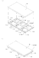
導電部形成工程は、前記めっき形成壁部12Wとグラウンドを電気的に接続させる工程である。
導電部形成工程は、基板ごとに個片化した状態で行う。個片化工程では、めっき形成壁部12Wと複数の基板からなるウエハ11Wは、切断されている。切断されたときの形態を図19に示す。切断後のめっき形成壁部12Wを壁部12、切断後の基板を基板部11とする。
導電部形成工程は、めっき形成壁部12Wとグラウンドを電気的に接続させるため、壁部12と基板の他方の主面の外部接続端子15の所定の一つと電気的に接続させる工程である。
電気的に接続させる方法として、スパッタリング法・蒸着法といった金属膜により導電させる方法、導電性のワイヤーを用いて導電させる方法、導電性接着剤やシール等を用いて導電させる方法などが挙げられる。電気的に接続させる方法については、指定しない。
図10は、第二の実施形態の圧電デバイス用容器体の製造工程の一部である導電部形成工程後の形態の概略図である。
The conductive portion forming step is a step of electrically connecting the plating forming wall portion 12W and the ground.
The conductive portion forming step is performed in a state of being separated into pieces for each substrate. In the singulation process, the plating forming wall portion 12W and the wafer 11W composed of a plurality of substrates are cut. The form when cut is shown in FIG. The plate forming wall portion 12W after cutting is referred to as a
The conductive portion forming step is a step of electrically connecting the
Examples of the electrical connection method include a method of conducting with a metal film such as a sputtering method or a vapor deposition method, a method of conducting with a conductive wire, a method of conducting with a conductive adhesive or a seal, and the like. The method of electrical connection is not specified.
FIG. 10 is a schematic view of a form after a conductive part forming step which is a part of the manufacturing process of the piezoelectric device container body of the second embodiment.
この壁部12と外部接続端子15と電気的に接続されている個片化された基板が、本発明の電子部品用容器体となる。
The board | substrate separated into pieces electrically connected with this
この電子部品用容器体の製造方法を用いることによって、主な工程をウエハ状態で処理することができるようになるため、生産コストの安い電子部品用容器体を製造することができる。 By using this method for manufacturing an electronic component container, the main steps can be processed in a wafer state, and thus an electronic component container having a low production cost can be manufactured.
この電子部品用容器体の製造方法は、壁部12が金属によって形成されているので電気的特性の悪化と周波数の安定した圧電振動子を提供することができる。
This method of manufacturing an electronic component container can provide a piezoelectric vibrator having a stable electric frequency and a stable frequency because the
11 水晶基板部
12 壁部
13 配線パターン
14 貫通孔
15 外部接続端子
16 導電部
11W 複数の基板からなる水晶ウエハ
12W 水晶ウエハの一方の主面に形成されためっき形成壁部
12MW 水晶ウエハの一方の主面に形成されためっき用金属層
R レジスト
DESCRIPTION OF SYMBOLS 11
Claims (3)
前記めっき用金属層と重なる部分の前記レジストを除去する第一のレジスト除去工程と、
電解めっき又は無電解めっきにより、前記めっき用金属層に所定の金属からなり且つ前記レジストと同じ厚みとなるめっき形成壁部を設けるめっき工程と、
前記ウエハの一方の主面に付着しているレジストを全て除去する第二のレジスト除去工程と、
前記めっき形成壁部の前記ウエハと平行となる面を平滑にする平滑工程と、
前記ウエハを基板ごとに個片化し、各基板の一方の主面に壁部を有する電子部品用容器体を得る個片化工程と、
からなることを特徴とする電子部品用容器体の製造方法。 A wiring pattern provided with a pair of metal layers for plating connected to the ground provided along the edge of the portion to be the substrate, and a pair of the metal layers for plating provided with a portion to be a plurality of substrates To one main surface of the wafer having external connection terminals provided at the four corners of the portion to be the substrate on the other main surface, with the resist having the same thickness as the wall portion described later A resist adhesion process to be adhered;
A first resist removing step of removing the resist in a portion overlapping the metal layer for plating;
A plating step of providing a plating forming wall portion made of a predetermined metal and having the same thickness as the resist by electrolytic plating or electroless plating;
A second resist removing step for removing all of the resist adhering to one main surface of the wafer;
A smoothing step of smoothing a surface parallel to the wafer of the plating forming wall;
The wafer is separated into individual substrates, and an individualization step for obtaining an electronic component container having a wall on one main surface of each substrate;
Method of manufacturing an electronic component container body, characterized in Tona Rukoto.
前記めっき用金属層と重なる部分の前記レジストを除去する第一のレジスト除去工程と、
電解めっき又は無電解めっきにより、前記めっき用金属層に所定の金属からなり且つ前記レジストと同じ厚みとなるめっき形成壁部を設けるめっき工程と、
前記ウエハの一方の主面に付着しているレジストを全て除去する第二のレジスト除去工程と、
前記めっき形成壁部の前記ウエハと平行となる面を平滑にする平滑工程と、
前記ウエハを基板ごとに個片化し、各基板の一方の主面に壁部を有する電子部品用容器体を得る個片化工程と、
前記壁部と前記外部接続端子のうちグラウンドとなる前記外部接続端子とを電気的に接続する導電部を、前記電子部品用容器体の外側面に形成する導電部形成工程と、
からなることを特徴とする電子部品用容器体の製造方法。 A portion to be a plurality of substrates is provided, and a plating metal layer provided along an edge of the portion to be the substrate and a wiring pattern provided in pairs inside the plating metal layer as one main Resist adhesion for attaching a resist to the same thickness as a wall portion described later on the one main surface of the wafer having external connection terminals provided at the four corners of the portion to be the substrate on the other main surface. Process,
A first resist removing step of removing the resist in a portion overlapping the metal layer for plating;
By electrolytic plating or electroless plating, a plating step of forming a Rumekki formed wall such as the same thickness as Do Ri and the resist from a predetermined metal to the plating metal layer,
A second resist removing step for removing all of the resist adhering to one main surface of the wafer;
A smoothing step of smoothing a surface parallel to the wafer of the plating forming wall;
The wafer is separated into individual substrates, and an individualization step for obtaining an electronic component container having a wall on one main surface of each substrate ;
A conductive portion forming step for forming a conductive portion that electrically connects the wall portion and the external connection terminal serving as a ground among the external connection terminals on an outer surface of the electronic component container body ;
The manufacturing method of the container for electronic components characterized by these.
Priority Applications (1)
| Application Number | Priority Date | Filing Date | Title |
|---|---|---|---|
| JP2008255705A JP5240913B2 (en) | 2008-09-30 | 2008-09-30 | Method for manufacturing container for electronic component |
Applications Claiming Priority (1)
| Application Number | Priority Date | Filing Date | Title |
|---|---|---|---|
| JP2008255705A JP5240913B2 (en) | 2008-09-30 | 2008-09-30 | Method for manufacturing container for electronic component |
Publications (2)
| Publication Number | Publication Date |
|---|---|
| JP2010087926A JP2010087926A (en) | 2010-04-15 |
| JP5240913B2 true JP5240913B2 (en) | 2013-07-17 |
Family
ID=42251404
Family Applications (1)
| Application Number | Title | Priority Date | Filing Date |
|---|---|---|---|
| JP2008255705A Active JP5240913B2 (en) | 2008-09-30 | 2008-09-30 | Method for manufacturing container for electronic component |
Country Status (1)
| Country | Link |
|---|---|
| JP (1) | JP5240913B2 (en) |
Families Citing this family (2)
| Publication number | Priority date | Publication date | Assignee | Title |
|---|---|---|---|---|
| JP2015056606A (en) * | 2013-09-13 | 2015-03-23 | 株式会社東芝 | Semiconductor device |
| JP7211081B2 (en) | 2018-12-28 | 2023-01-24 | セイコーエプソン株式会社 | vibration device |
Family Cites Families (3)
| Publication number | Priority date | Publication date | Assignee | Title |
|---|---|---|---|---|
| JP2003087071A (en) * | 2001-09-14 | 2003-03-20 | Toyo Commun Equip Co Ltd | Surface-mounted type piezoelectric device and manufacturing method therefor |
| JP2005065104A (en) * | 2003-08-19 | 2005-03-10 | Murata Mfg Co Ltd | Surface mounted piezoelectric vibrator and its manufacturing method |
| JP2007027279A (en) * | 2005-07-13 | 2007-02-01 | Shinko Electric Ind Co Ltd | Semiconductor device and manufacturing method thereof |
-
2008
- 2008-09-30 JP JP2008255705A patent/JP5240913B2/en active Active
Also Published As
| Publication number | Publication date |
|---|---|
| JP2010087926A (en) | 2010-04-15 |
Similar Documents
| Publication | Publication Date | Title |
|---|---|---|
| JP5054703B2 (en) | MEMS microphone, method for manufacturing MEMS microphone, and method for incorporating MEMS microphone | |
| US8991022B2 (en) | Method for manufacturing piezoelectric resonator device | |
| JP2006203700A (en) | Method for manufacturing piezoelectric substrate, piezoelectric vibration element, piezoelectric vibrator and piezo-oscillator | |
| TWI517310B (en) | Manufacturing method of electronic device package | |
| US20060290238A1 (en) | Electronic part having high sealing performance and method of manufacturing the same | |
| JP2012084954A (en) | Acoustic wave element and electronic device using the same | |
| US7876168B2 (en) | Piezoelectric oscillator and method for manufacturing the same | |
| JP5171210B2 (en) | Method for manufacturing piezoelectric vibrator | |
| JP5240913B2 (en) | Method for manufacturing container for electronic component | |
| JP4010293B2 (en) | Metal package manufacturing method | |
| JP4706399B2 (en) | Oscillator and electronic equipment | |
| JP2015211362A (en) | Quarts device and manufacturing method for quarts device | |
| JP2010130400A (en) | Piezoelectric vibration device | |
| JP2008252805A (en) | Crystal oscillator and method of producing crystal oscillator | |
| WO2017135395A1 (en) | Through-electrode substrate and method for manufacturing same | |
| JP2004356687A (en) | Manufacturing method for piezoelectric vibration device and piezoelectric vibration device manufactured by the method | |
| JP2011182064A (en) | Crystal resonator for surface mounting | |
| JP4673670B2 (en) | Method for manufacturing piezoelectric device | |
| JP4605083B2 (en) | Method for manufacturing piezoelectric vibrating piece | |
| JP2009111931A (en) | Piezoelectric vibrator and method for manufacturing piezoelectric vibrator | |
| JP5513047B2 (en) | Electronic device and method for manufacturing electronic device | |
| JP2008159844A (en) | Electronic component package structure and its method for manufacturing | |
| JP2008035276A (en) | Method of manufacturing piezoelectric oscillator | |
| JP2009182873A (en) | Method for manufacturing piezoelectric oscillation device, and piezoelectric oscillation device | |
| JP4692619B2 (en) | Quartz vibrating piece, manufacturing method thereof, quartz crystal device using quartz crystal vibrating piece, mobile phone device using quartz crystal device, and electronic equipment using quartz crystal device |
Legal Events
| Date | Code | Title | Description |
|---|---|---|---|
| A621 | Written request for application examination |
Free format text: JAPANESE INTERMEDIATE CODE: A621 Effective date: 20110909 |
|
| A977 | Report on retrieval |
Free format text: JAPANESE INTERMEDIATE CODE: A971007 Effective date: 20121221 |
|
| A131 | Notification of reasons for refusal |
Free format text: JAPANESE INTERMEDIATE CODE: A131 Effective date: 20130108 |
|
| A521 | Written amendment |
Free format text: JAPANESE INTERMEDIATE CODE: A523 Effective date: 20130306 |
|
| TRDD | Decision of grant or rejection written | ||
| A01 | Written decision to grant a patent or to grant a registration (utility model) |
Free format text: JAPANESE INTERMEDIATE CODE: A01 Effective date: 20130327 |
|
| A61 | First payment of annual fees (during grant procedure) |
Free format text: JAPANESE INTERMEDIATE CODE: A61 Effective date: 20130329 |
|
| FPAY | Renewal fee payment (event date is renewal date of database) |
Free format text: PAYMENT UNTIL: 20160412 Year of fee payment: 3 |
|
| R150 | Certificate of patent or registration of utility model |
Free format text: JAPANESE INTERMEDIATE CODE: R150 Ref document number: 5240913 Country of ref document: JP Free format text: JAPANESE INTERMEDIATE CODE: R150 |
|
| R250 | Receipt of annual fees |
Free format text: JAPANESE INTERMEDIATE CODE: R250 |
|
| R250 | Receipt of annual fees |
Free format text: JAPANESE INTERMEDIATE CODE: R250 |
|
| S111 | Request for change of ownership or part of ownership |
Free format text: JAPANESE INTERMEDIATE CODE: R313111 |
|
| R350 | Written notification of registration of transfer |
Free format text: JAPANESE INTERMEDIATE CODE: R350 |