JP5233272B2 - Power supply circuit, display driver, electro-optical device, and electronic device - Google Patents
Power supply circuit, display driver, electro-optical device, and electronic device Download PDFInfo
- Publication number
- JP5233272B2 JP5233272B2 JP2007327194A JP2007327194A JP5233272B2 JP 5233272 B2 JP5233272 B2 JP 5233272B2 JP 2007327194 A JP2007327194 A JP 2007327194A JP 2007327194 A JP2007327194 A JP 2007327194A JP 5233272 B2 JP5233272 B2 JP 5233272B2
- Authority
- JP
- Japan
- Prior art keywords
- voltage
- power supply
- circuit
- supply circuit
- charge pump
- Prior art date
- Legal status (The legal status is an assumption and is not a legal conclusion. Google has not performed a legal analysis and makes no representation as to the accuracy of the status listed.)
- Active
Links
Images


Landscapes
- Liquid Crystal (AREA)
- Liquid Crystal Display Device Control (AREA)
- Control Of Indicators Other Than Cathode Ray Tubes (AREA)
- Dc-Dc Converters (AREA)
Description
本発明は、電源回路、表示ドライバ、電気光学装置及び電子機器等に関する。 The present invention relates to a power supply circuit, a display driver, an electro-optical device, an electronic apparatus, and the like.
携帯型の電子機器には、より一層の低消費電力化が求められる。このような電子機器に搭載される表示装置として、液晶表示装置が用いられることが多い。液晶表示装置を駆動するためには、高い電圧や負の電圧等の複数の電源を必要とする。この場合、液晶表示装置を駆動する液晶駆動装置は、複数の電源を生成する電源回路を内蔵することがコストの観点からも望ましい。 Portable electronic devices are required to further reduce power consumption. A liquid crystal display device is often used as a display device mounted on such an electronic device. In order to drive the liquid crystal display device, a plurality of power sources such as a high voltage and a negative voltage are required. In this case, it is desirable from the viewpoint of cost that the liquid crystal driving device that drives the liquid crystal display device incorporates a power supply circuit that generates a plurality of power supplies.
このような電源回路は、昇圧回路を含む。この昇圧回路として、例えば特許文献1に記載されるようなチャージポンプ動作により昇圧した電圧を生成するチャージポンプ回路が採用されることが多い。チャージポンプ回路は、電荷を蓄積したコンデンサの一端を、スイッチ素子(例えば金属酸化膜半導体(Metal Oxide Semiconductor:MOS)トランジスタ)により各種電圧に接続していくことで、該コンデンサに蓄積された電荷に対応した電圧を昇圧していく。このようなチャージポンプ回路を用いることで、低消費化を図ることができる。
昇圧回路の電力効率という観点から、昇圧回路の出力負荷をできるだけ小さくすることが望ましい。そのため、例えば特許文献1のように、昇圧回路の出力が、そのまま昇圧回路の出力電圧の供給対象の回路に接続される。
From the viewpoint of the power efficiency of the booster circuit, it is desirable to make the output load of the booster circuit as small as possible. Therefore, for example, as in
また、昇圧回路の出力電位を調整する際には、レギュレータが用いられる。このとき、低消費電力化を目的として、該レギュレータをできるだけ低い動作電圧で動作させることが望ましい。そのため、昇圧回路で昇圧した電圧をレギュレータで調整するのではなく、レギュレータで電圧を調整してから、調整後の電圧が昇圧回路に入力される。この場合、レギュレータによる調整後の電圧を昇圧する昇圧回路の電圧がターゲット電圧を超える場合、超過分の電圧を降圧するためにシステム接地電源に電荷を放電することが行われる。例えば、3.3Vの電圧を2倍昇圧する場合、集積回路装置の絶対最大定格となる6V以下となるように、0.6V(=3.3×2−6)だけ電位が下がるように電荷が放電される。従って、この超過分の電圧を調整するための電荷の充放電量を減らすことができれば、電源回路の低消費電力化を実現できる。 A regulator is used to adjust the output potential of the booster circuit. At this time, it is desirable to operate the regulator with the lowest possible operating voltage for the purpose of reducing power consumption. Therefore, the voltage boosted by the booster circuit is not adjusted by the regulator, but the adjusted voltage is input to the booster circuit after the voltage is adjusted by the regulator. In this case, when the voltage of the booster circuit that boosts the voltage adjusted by the regulator exceeds the target voltage, the electric charge is discharged to the system ground power source in order to step down the excess voltage. For example, when the voltage of 3.3 V is boosted twice, the electric charge is reduced so that the potential is lowered by 0.6 V (= 3.3 × 2−6) so that the absolute maximum rating of the integrated circuit device is 6 V or less. Is discharged. Therefore, if the charge / discharge amount for adjusting the excess voltage can be reduced, the power consumption of the power supply circuit can be reduced.
また、電源回路の出力負荷に応じて、電源回路の電力効率が変動する。これは、出力負荷によって、無駄な電力を使って昇圧動作を行ってしまうことを意味する。従って、電源回路の出力負荷に応じて昇圧能力を変更でき、且つ出力負荷に対して安定した電圧を供給できるように昇圧能力を変更できることが望ましい。 Further, the power efficiency of the power supply circuit varies depending on the output load of the power supply circuit. This means that the boost operation is performed using wasted power depending on the output load. Therefore, it is desirable that the boosting capability can be changed according to the output load of the power supply circuit and the boosting capability can be changed so that a stable voltage can be supplied to the output load.
本発明の幾つかの態様によれば、出力負荷が高くなっても昇圧能力を低下させることなく低消費電力で昇圧電圧を供給できる電源回路、表示ドライバ、電気光学装置及び電子機器を提供できる。 According to some aspects of the present invention, it is possible to provide a power supply circuit, a display driver, an electro-optical device, and an electronic apparatus that can supply a boosted voltage with low power consumption without reducing the boosting capability even when the output load increases.
上記課題を解決するために本発明は、
昇圧した電圧を出力するための電源回路であって、
第1の電圧を基準に第2の電圧を昇圧した昇圧電圧を生成する昇圧回路と、
前記昇圧電圧の電位を制限するリミッタ回路とを含み、
前記リミッタ回路が、
前記昇圧電圧が所与のターゲット電圧になるように前記第2の電圧が供給される電源線に電荷を放電、又は該電源線から電荷を充電し、
前記昇圧回路が、
前記電源回路の出力負荷に応じて、昇圧能力を変更する電源回路に関係する。
In order to solve the above problems, the present invention
A power supply circuit for outputting a boosted voltage,
A booster circuit that generates a boosted voltage obtained by boosting the second voltage with reference to the first voltage;
A limiter circuit for limiting the potential of the boosted voltage,
The limiter circuit is
Discharging the charge to the power supply line to which the second voltage is supplied so that the boosted voltage becomes a given target voltage, or charging the charge from the power supply line,
The booster circuit is
The present invention relates to a power supply circuit that changes the boosting capability according to the output load of the power supply circuit.
本発明に係る電源回路では、リミッタ回路において、昇圧電圧が所与のターゲット電圧になるように、昇圧元の電源である、第2の電圧が供給される電源線に電荷を放電、又は該電源線から電荷を充電するようにしたので、電荷を再利用でき電源回路の低消費電力化を実現できるようになる。 In the power supply circuit according to the present invention, in the limiter circuit, the charge is discharged to the power supply line to which the second voltage, which is the power source of the boost source, is supplied, or the power source so that the boost voltage becomes a given target voltage. Since the charge is charged from the line, the charge can be reused and the power consumption of the power supply circuit can be reduced.
更に、昇圧回路が、電源回路の出力負荷に応じて昇圧能力を変更するようにしたので、出力負荷が高い場合でも昇圧能力を低下させることなく、且つ出力負荷に対して昇圧効率が低下することを防止できるようになる。 Furthermore, since the booster circuit changes the boosting capability according to the output load of the power supply circuit, even if the output load is high, the boosting capability is not lowered with respect to the output load without decreasing the boosting capability. Can be prevented.
また本発明に係る電源回路では、
前記出力負荷に対して前記昇圧能力が高いと判断されるときには、昇圧能力がより低くなるように該昇圧能力を変更し、
前記出力負荷に対して前記昇圧能力が低いと判断されるときには、昇圧能力がより高くなるように該昇圧能力を変更することができる。
In the power supply circuit according to the present invention,
When it is determined that the boost capability is high with respect to the output load, the boost capability is changed so that the boost capability becomes lower,
When it is determined that the boosting capability is low with respect to the output load, the boosting capability can be changed so that the boosting capability becomes higher.
本発明によれば、出力負荷に応じて昇圧能力を適正なレベルに維持できるので、昇圧能力により得られる電圧を安定化させつつ、且つ出力負荷に対して昇圧効率が低下することを防止できるようになる。 According to the present invention, since the boosting capability can be maintained at an appropriate level according to the output load, it is possible to stabilize the voltage obtained by the boosting capability and prevent the boosting efficiency from decreasing with respect to the output load. become.
また本発明に係る電源回路では、
前記昇圧回路が、
前記出力負荷と、前記リミッタ回路が前記昇圧電圧の電位を制限したか否かを示すリミッタ動作情報とに基づいて、前記昇圧能力を変更することができる。
In the power supply circuit according to the present invention,
The booster circuit is
The boosting capability can be changed based on the output load and limiter operation information indicating whether or not the limiter circuit has limited the potential of the boosted voltage.
また本発明に係る電源回路では、
前記昇圧回路が、
前記リミッタ情報に基づいて更新される閾値と、前記出力負荷との比較結果に応じて、前記昇圧能力を変更することができる。
In the power supply circuit according to the present invention,
The booster circuit is
The boosting capability can be changed according to a comparison result between the threshold value updated based on the limiter information and the output load.
また本発明に係る電源回路では、
前記閾値が、
所与の閾値電圧と前記昇圧電圧との比較結果に基づいて更新されてもよい。
In the power supply circuit according to the present invention,
The threshold is
It may be updated based on a comparison result between a given threshold voltage and the boosted voltage.
また本発明に係る電源回路では、
前記所与の閾値電圧と前記昇圧電圧とを比較するコンパレータと、
前記コンパレータの出力結果のパルス幅又はパルス数をカウントするカウンタとを含み、
前記閾値が、
前記カウンタのカウント数に基づいて更新されてもよい。
In the power supply circuit according to the present invention,
A comparator for comparing the given threshold voltage with the boost voltage;
A counter that counts the pulse width or number of pulses of the output result of the comparator,
The threshold is
It may be updated based on the count number of the counter.
上記のいずれかの発明によれば、リミッタ回路の動作情報に基づいて昇圧能力を変更できるようにしたので、種々の出力負荷に対して、最適な昇圧能力で低消費電力動作が可能な電源回路を提供できる。 According to any one of the above-described inventions, since the boosting capability can be changed based on the operation information of the limiter circuit, the power supply circuit capable of low power consumption operation with the optimum boosting capability for various output loads Can provide.
また本発明に係る電源回路では、
電気光学装置の複数のソース線の各ソース線の階調データに対応した駆動電圧が、前記昇圧電圧に基づいて生成される場合に、
前記出力負荷が、
前記複数のソース線の1走査ライン分の階調データの総和に基づいて評価されてもよい。
In the power supply circuit according to the present invention,
When a driving voltage corresponding to gradation data of each source line of the plurality of source lines of the electro-optical device is generated based on the boosted voltage,
The output load is
The evaluation may be based on the sum of gradation data for one scanning line of the plurality of source lines.
本発明によれば、出力負荷を簡素な構成で評価できるようになる。 According to the present invention, the output load can be evaluated with a simple configuration.
また本発明に係る電源回路では、
前記昇圧回路が、
第1のフライングコンデンサを用いたチャージポンプ動作により、前記昇圧電圧を生成するための第1のチャージポンプ回路と、
前記第1のフライングコンデンサより容量値の大きい第2のフライングコンデンサを用いたチャージポンプ動作により、前記昇圧電圧を生成するための第2のチャージポンプ回路とを含み、
前記昇圧回路の昇圧能力の変更後に、前記第1のチャージポンプ回路により生成された昇圧電圧、前記第2のチャージポンプ回路により生成された昇圧電圧、又は前記第1及び第2のチャージポンプ回路により生成された昇圧電圧を出力することができる。
In the power supply circuit according to the present invention,
The booster circuit is
A first charge pump circuit for generating the boosted voltage by a charge pump operation using a first flying capacitor;
A second charge pump circuit for generating the boosted voltage by a charge pump operation using a second flying capacitor having a larger capacitance value than the first flying capacitor;
After the boosting capability of the booster circuit is changed, the boosted voltage generated by the first charge pump circuit, the boosted voltage generated by the second charge pump circuit, or the first and second charge pump circuits. The generated boosted voltage can be output.
本発明によれば、簡素な構成で、昇圧回路の昇圧能力を変更できるようになる。 According to the present invention, the boosting capability of the booster circuit can be changed with a simple configuration.
また本発明は、
電気光学装置を駆動するための表示ドライバであって、
上記のいずれか記載の電源回路と、
前記電気光学装置を駆動するための駆動部とを含み、
前記昇圧電圧に基づいて、前記駆動部の駆動電圧を生成する表示ドライバに関係する。
The present invention also provides
A display driver for driving an electro-optical device,
Any one of the power supply circuits described above;
A drive unit for driving the electro-optical device,
The present invention relates to a display driver that generates a driving voltage of the driving unit based on the boosted voltage.
また本発明に係る表示ドライバでは、
前記駆動部が、
前記昇圧電圧を用いて生成された、階調データに対応した駆動電圧により前記電気光学装置の複数のソース線を駆動することができる。
In the display driver according to the present invention,
The drive unit is
A plurality of source lines of the electro-optical device can be driven by a driving voltage corresponding to the gradation data generated using the boosted voltage.
上記のいずれかの発明によれば、出力負荷が高くなっても昇圧能力を低下させることなく低消費電力で昇圧電圧を供給できる電源回路が適用された表示ドライバを提供できる。 According to any one of the above-described inventions, it is possible to provide a display driver to which a power supply circuit that can supply a boosted voltage with low power consumption without reducing the boosting capability even when the output load becomes high.
また本発明は、
複数のゲート線と、
複数のソース線と、
前記複数のゲート線を走査するゲートドライバと、
前記複数のソース線を駆動するソースドライバと、
上記のいずれか記載の電源回路とを含み、
前記ゲートドライバの走査電圧及び前記ソースドライバの駆動電圧のうち少なくとも1つが、前記昇圧電圧に基づいて生成される電気光学装置に関係する。
The present invention also provides
Multiple gate lines,
Multiple source lines,
A gate driver that scans the plurality of gate lines;
A source driver for driving the plurality of source lines;
Including any of the power supply circuits described above,
At least one of the scanning voltage of the gate driver and the driving voltage of the source driver is related to the electro-optical device generated based on the boosted voltage.
また本発明は、
複数のゲート線と、
複数のソース線と、
前記複数のゲート線を走査するゲートドライバと、
前記複数のソース線を駆動する上記記載の表示ドライバとを含む電気光学装置に関係する。
The present invention also provides
Multiple gate lines,
Multiple source lines,
A gate driver that scans the plurality of gate lines;
The present invention relates to an electro-optical device including the display driver described above that drives the plurality of source lines.
上記のいずれかの発明によれば、出力負荷が高くなっても昇圧能力を低下させることなく低消費電力で昇圧電圧を供給できる電源回路が適用された電気光学装置を提供できる。 According to any one of the above-described inventions, it is possible to provide an electro-optical device to which a power supply circuit that can supply a boosted voltage with low power consumption without reducing the boosting capability even when the output load becomes high.
また本発明は、
上記のいずれか記載の電源回路を含む電子機器に関係する。
The present invention also provides
The present invention relates to an electronic device including any one of the power supply circuits described above.
また本発明は、
上記記載の表示ドライバを含む電子機器に関係する。
The present invention also provides
The present invention relates to an electronic device including the display driver described above.
また本発明は、
上記記載の電気光学装置を含む電子機器に関係する。
The present invention also provides
The present invention relates to an electronic apparatus including the electro-optical device described above.
上記のいずれかの発明によれば、出力負荷が高くなっても昇圧能力を低下させることなく低消費電力で昇圧電圧を供給できる電源回路が適用された電子機器を提供できる。 According to any one of the above-described inventions, it is possible to provide an electronic apparatus to which a power supply circuit that can supply a boosted voltage with low power consumption without reducing the boosting capability even when the output load increases.
以下、本発明の実施の形態について図面を用いて詳細に説明する。なお、以下に説明する実施の形態は、特許請求の範囲に記載された本発明の内容を不当に限定するものではない。また以下で説明される構成のすべてが本発明の必須構成要件であるとは限らない。 Hereinafter, embodiments of the present invention will be described in detail with reference to the drawings. The embodiments described below do not unduly limit the contents of the present invention described in the claims. Also, not all of the configurations described below are essential constituent requirements of the present invention.
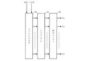
1. 液晶表示装置
図1に、本実施形態の液晶表示装置のブロック図の例を示す。
1. Liquid Crystal Display Device FIG. 1 shows an example of a block diagram of a liquid crystal display device of this embodiment.
液晶表示装置10(液晶装置。広義には電気光学装置)は、表示パネル12(狭義には液晶パネル、LCD(Liquid Crystal Display)パネル、広義には電気光学パネル)、ソースドライバ20(広義にはデータ線駆動回路)、ゲートドライバ30(広義には走査線駆動回路)、表示コントローラ40、電源回路50を含む。なお、液晶表示装置10にこれらのすべての回路ブロックを含める必要はなく、その一部の回路ブロックを省略する構成にしてもよい。電気光学装置は、有機EL(Electro Luminescence)、無機EL素子等の発光素子を用いた装置を含むことができる。
The liquid crystal display device 10 (liquid crystal device; electro-optical device in a broad sense) includes a display panel 12 (a liquid crystal panel in a narrow sense, an LCD (Liquid Crystal Display) panel, an electro-optical panel in a broad sense), and a source driver 20 (in a broad sense). Data line driving circuit), gate driver 30 (scanning line driving circuit in a broad sense),
ここで表示パネル12(電気光学装置)は、複数のゲート線(広義には走査線)と、複数のソース線(広義にはデータ線)と、ゲート線及びソース線により特定される画素電極を含む。この場合、ソース線に薄膜トランジスタTFT(Thin Film Transistor、広義にはスイッチング素子)を接続し、このTFTに画素電極を接続することで、アクティブマトリクス型の液晶表示装置を構成できる。 Here, the display panel 12 (electro-optical device) includes a plurality of gate lines (scanning lines in a broad sense), a plurality of source lines (data lines in a broad sense), and pixel electrodes specified by the gate lines and the source lines. Including. In this case, an active matrix liquid crystal display device can be configured by connecting a thin film transistor TFT (Thin Film Transistor, switching element in a broad sense) to a source line and connecting a pixel electrode to the TFT.
より具体的には、表示パネル12は、アクティブマトリクス基板(例えばガラス基板)上にアモルファスシリコン薄膜が形成されたアモルファスシリコン液晶パネルである。アクティブマトリクス基板には、図1のY方向に複数配列されそれぞれX方向に伸びるゲート線G1〜GM(Mは2以上の自然数)と、X方向に複数配列されそれぞれY方向に伸びるソース線S1〜SN(Nは2以上の自然数)とが配置されている。また、ゲート線GK(1≦K≦M、Kは自然数)とソース線SL(1≦L≦N、Lは自然数)との交差点に対応する位置に、薄膜トランジスタTFTKL(広義にはスイッチング素子)が設けられている。
More specifically, the
TFTKLのゲート電極はゲート線GKに接続され、TFTKLのソース電極はソース線SLに接続され、TFTKLのドレイン電極は画素電極PEKLに接続されている。この画素電極PEKLと、画素電極PEKLと液晶(広義には電気光学物質)を挟んで対向する対向電極CE(共通電極、コモン電極)との間には、素子容量である液晶容量CLKL(液晶素子)、及び補助容量CSKLが形成されている。そして、TFTKL、画素電極PEKL等が形成されるアクティブマトリクス基板と対向電極CEが形成される対向基板との間に液晶が封入されるように形成され、画素電極PEKLと対向電極CEとの間の印加電圧に応じて画素の透過率が変化するようになっている。素子容量は、液晶素子に形成される液晶容量や、無機EL素子等のEL素子に形成される容量を含むことができる。 The gate electrode of the thin film transistor TFT KL is connected with the gate line G K, a source electrode of the thin film transistor TFT KL is connected with the source line S L, the drain electrode of the thin film transistor TFT KL is connected with a pixel electrode PE KL. Between the pixel electrode PE KL and the counter electrode CE (common electrode, common electrode) facing the pixel electrode PE KL with a liquid crystal (electro-optical material in a broad sense) interposed therebetween, a liquid crystal capacitance CL KL which is an element capacitance (Liquid crystal element) and auxiliary capacitor CS KL are formed. Then, liquid crystal is formed between the active matrix substrate on which the TFT KL , the pixel electrode PE KL, and the like are formed and the counter substrate on which the counter electrode CE is formed, and the pixel electrode PE KL , the counter electrode CE, The transmittance of the pixel is changed in accordance with the applied voltage between. The element capacitance can include a liquid crystal capacitance formed in a liquid crystal element and a capacitance formed in an EL element such as an inorganic EL element.
なお、対向電極CEに与えられる対向電極電圧VCOMの電圧レベル(高電位側電圧VCOMH、低電位側電圧VCOML)は、電源回路50に含まれる対向電極電圧生成回路より生成される。例えば、対向電極CEは、対向基板上に一面に形成される。
Note that the voltage level (high potential side voltage VCOMH, low potential side voltage VCOML) of the counter electrode voltage VCOM applied to the counter electrode CE is generated by a counter electrode voltage generation circuit included in the
ソースドライバ20は、階調データに基づいて表示パネル12のソース線S1〜SNを駆動する。一方、ゲートドライバ30は、表示パネル12のゲート線G1〜GMを走査(順次駆動)する。
The
表示コントローラ40は、図示しない中央演算処理装置(Central Processing Unit:CPU)等のホストにより設定された内容に従って、ソースドライバ20、ゲートドライバ30及び電源回路50を制御する。より具体的には、表示コントローラ40は、ソースドライバ20及びゲートドライバ30に対しては、例えば動作モードの設定や内部で生成した垂直同期信号や水平同期信号の供給を行い、電源回路50に対しては、対向電極CEに印加する対向電極電圧VCOMの電圧レベルの極性反転タイミングの制御を行う。
The
電源回路50は、外部から供給されるシステム電源電圧を昇圧するなどして、表示パネル12の駆動に必要な各種の電圧レベル(階調電圧)や、対向電極CEの対向電極電圧VCOMの電圧レベルを生成する。本実施形態における電源回路50は、電源回路50の出力負荷を評価するための評価値をソースドライバ20から受け、該評価値に基づいて昇圧能力を変更できるようになっている。ここで、昇圧能力は、出力負荷電流の変化に対して出力電圧を変化させる能力ということができる。
The
このように、ソースドライバ20及びゲートドライバ30を、表示パネル12を駆動するための駆動部とした場合に、電源回路50により昇圧された電圧に基づいて、駆動部の駆動電圧を生成することができる。
As described above, when the
このような構成の液晶表示装置10は、表示コントローラ40の制御の下、外部から供給される階調データに基づいて、ソースドライバ20、ゲートドライバ30及び電源回路50が協調して表示パネル12を駆動する。
In the liquid
なお、図1では、液晶表示装置10が表示コントローラ40を含む構成になっているが、表示コントローラ40を液晶表示装置10の外部に設けてもよい。或いは、表示コントローラ40と共にホストを液晶表示装置10に含めるようにしてもよい。また、ソースドライバ20、ゲートドライバ30、表示コントローラ40、電源回路50の一部又は全部を表示パネル12上に形成してもよい。
In FIG. 1, the liquid
また図1において、ソースドライバ20、ゲートドライバ30及び電源回路50を集積化して、半導体装置(集積回路、IC)として表示ドライバ60を構成してもよい。
In FIG. 1, the
図2に、本実施形態における液晶表示装置の他の構成例のブロック図を示す。 FIG. 2 is a block diagram showing another configuration example of the liquid crystal display device according to this embodiment.
図2では、表示パネル12上(パネル基板上)に、ソースドライバ20、ゲートドライバ30及び電源回路50を含む表示ドライバ60が形成されている。このように表示パネル12は、複数のゲート線と、複数のソース線と、複数のゲート線の各ゲート線及び複数のソース線の各ソース線とに接続された複数の画素(画素電極)と、複数のソース線を駆動するソースドライバと、複数のゲート線を走査するゲートドライバとを含むように構成することができる。表示パネル12の画素形成領域44に、複数の画素が形成されている。各画素は、ソースにソース線が接続されゲートにゲート線が接続されたTFTと、該TFTのドレインに接続された画素電極とを含むことができる。
In FIG. 2, a
なお図2では、表示パネル12上においてゲートドライバ30及び電源回路50のうち少なくとも1つが省略された構成であってもよい。
In FIG. 2, at least one of the
また図1又は図2において、表示ドライバ60が、表示コントローラ40を内蔵してもよい。或いは図1又は図2において、表示ドライバ60が、ソースドライバ20及びゲートドライバ30のいずれか一方と、電源回路50とを集積化した半導体装置であってもよい。
In FIG. 1 or FIG. 2, the
1.1 ゲートドライバ
図3に、図1又は図2のゲートドライバ30の構成例を示す。
1.1 Gate Driver FIG. 3 shows a configuration example of the
ゲートドライバ30は、シフトレジスタ32、レベルシフタ34、出力バッファ36を含む。
The
シフトレジスタ32は、各ゲート線に対応して設けられ、順次接続された複数のフリップフロップを含む。このシフトレジスタ32は、クロック信号CLKに同期してイネーブル入出力信号EIOをフリップフロップに保持すると、順次クロック信号CLKに同期して隣接するフリップフロップにイネーブル入出力信号EIOをシフトする。ここで入力されるイネーブル入出力信号EIOは、表示コントローラ40から供給される垂直同期信号である。
The
レベルシフタ34は、シフトレジスタ32からの電圧レベルを、表示パネル12の液晶素子とTFTのトランジスタ能力とに応じた電圧レベルにシフトする。この電圧レベルとしては、高い電圧レベルが必要とされるため、他のロジック回路部とは異なる高耐圧プロセスが用いられる。
The
出力バッファ36は、レベルシフタ34によってシフトされた走査電圧をバッファリングしてゲート線に出力し、ゲート線を駆動する。
The
1.2 ソースドライバ
図4に、図1又は図2のソースドライバ20の構成例のブロック図を示す。
1.2 Source Driver FIG. 4 is a block diagram showing a configuration example of the
ソースドライバ20は、シフトレジスタ22、ラインラッチ24、26、階調データ総和演算部25、DAC28(Digital-to-Analog Converter)(広義にはデータ電圧生成回路)、ソース線駆動回路29を含む。
The
シフトレジスタ22は、各ソース線に対応して設けられ、順次接続された複数のフリップフロップを含む。このシフトレジスタ22は、クロック信号CLKに同期してイネーブル入出力信号EIOを保持すると、順次クロック信号CLKに同期して隣接するフリップフロップにイネーブル入出力信号EIOをシフトする。
The
ラインラッチ24には、表示コントローラ40から例えば18ビット(6ビット(階調データ)×3(RGB各色))単位で階調データ(DIO)が入力される。ラインラッチ24は、この階調データ(DIO)を、シフトレジスタ22の各フリップフロップで順次シフトされたイネーブル入出力信号EIOに同期してラッチする。
Gradation data (DIO) is input to the
ラインラッチ26は、表示コントローラ40から供給される水平同期信号LPに同期して、ラインラッチ24でラッチされた1水平走査単位の階調データをラッチする。
The
階調データ総和演算部25は、電源回路50の出力負荷を評価するための評価値を、階調データに基づいて演算する。この評価値は、総和データGSUMとして電源回路50に供給される。より具体的には、階調データ総和演算部25は、1走査ライン分の階調データを加算することで、評価値を求めることができる。例えば階調データ総和演算部25は、ラインラッチ26に取り込まれる階調データを1ソース出力毎に加算して総和データを求め、評価値とする。このような評価値としての総和データに基づいて、表示パネル12の駆動に用いられる階調電圧の大小を大まかに評価でき、電源回路50の出力負荷の評価に用いることができる。
The gradation data
基準電圧発生回路27は、64(=26)種類の基準電圧を生成する。基準電圧発生回路27によって生成された64種類の基準電圧は、DAC28に供給される。
The reference
DAC(データ電圧生成回路)28は、各ソース線に供給すべきアナログのデータ電圧を生成する。具体的にはDAC28は、ラインラッチ26からのデジタルの階調データに基づいて、基準電圧発生回路27からの基準電圧のいずれかを選択し、デジタルの階調データに対応するアナログのデータ電圧を出力する。
A DAC (data voltage generation circuit) 28 generates an analog data voltage to be supplied to each source line. Specifically, the
ソース線駆動回路29は、DAC28からのデータ電圧をバッファリングしてソース線に出力し、ソース線を駆動する。具体的には、ソース線駆動回路29は、各ソース線毎に設けられたボルテージフォロワ接続の演算増幅器OPC(広義にはインピーダンス変換回路)を含み、これらの各演算増幅器OPCが、DAC28からのデータ電圧をインピーダンス変換して、各ソース線に出力する。
The source
なお、図4では、デジタルの階調データをデジタル・アナログ変換して、ソース線駆動回路29を介してソース線に出力する構成を採用しているが、アナログの映像信号をサンプル・ホールドして、ソース線駆動回路29を介してソース線に出力する構成を採用することもできる。
In FIG. 4, the digital gradation data is converted from digital to analog and output to the source line via the source
図5に、図4の基準電圧発生回路27、DAC28及びソース線駆動回路29の構成例を示す。図5において、階調データが6ビットのデータD0〜D5であり、各ビットのデータの反転データをXD0〜XD5と示している。また図5において、図4と同一部分には同一符号を付し、適宜説明を省略する。
FIG. 5 shows a configuration example of the reference
基準電圧発生回路27は、両端の電圧VDDH、VSSHを抵抗分割して64種類の基準電圧を生成する。ここで、電圧VDDHは、電源回路50により得られた昇圧電圧VOUTとすることができる。各基準電圧は、6ビットの階調データにより表される各階調値に対応している。各基準電圧は、ソース線S1〜SNの各ソース線に共通に供給される。
The reference
DAC28は、ソース線毎に設けられたデコーダを含み、各デコーダは、階調データに対応した基準電圧を演算増幅器OPCに出力する。
The
1.3 電源回路
図6に、図1又は図2の電源回路50の構成例を示す。
1.3 Power Supply Circuit FIG. 6 shows a configuration example of the
電源回路50は、昇圧回路52、リミッタ回路53、走査電圧生成回路54、対向電極電圧生成回路56を含む。この電源回路50には、システム接地電源電圧VSS(第1の電圧)及びシステム電源電圧VDD(第2の電圧)が供給される。
The
昇圧回路52には、システム接地電源電圧VSS及びシステム電源電圧VDDが供給される。そして昇圧回路52は、システム接地電源電圧VSSを基準に、システム電源電圧VDDを正方向に例えば2倍に昇圧した電源電圧VOUT(昇圧電圧)を生成する。即ち昇圧回路52は、システム接地電源電圧VSSとシステム電源電圧VDDとの間の電圧差を2倍に昇圧する。このような昇圧回路52は、チャージポンプ回路により構成できる。電源電圧VOUTは、ソースドライバ20、走査電圧生成回路54や対向電極電圧生成回路56に供給される。ソースドライバ20は、電源電圧VOUTに基づいて、階調データに対応した階調電圧を生成する。また、ゲートドライバ30は、走査電圧生成回路54を含むことができ、この場合には、電源電圧VOUTに基づいて、走査電圧を生成するということができる。
The
リミッタ回路53は、昇圧回路52によって生成された電源電圧VOUT(昇圧電圧)が所与のターゲット電圧になるように、システム電源電圧VDD(第2の電圧)が供給される電源線に電荷を放電、又は該電源線から電荷を充電する。本実施形態では、昇圧回路52がシステム接地電源電圧VSSを基準に正方向に電圧を昇圧するため、システム電源電圧VDDが供給される電源線に正の電荷を放電(該電源線から負の電荷を充電)する。これにより、システム接地電源電圧VSS(第1の電圧)が供給される電源線に電荷を放電するよりも、電荷を再利用できるため低消費電力化を図ることができる。更に、本実施形態では、昇圧回路52が、電源回路50の出力負荷に応じて、昇圧能力を変更することができるようになっている。この電源回路50の出力負荷は、ソースドライバ20からの評価値としての総和データGSUMに基づいて評価される。
The
走査電圧生成回路54には、システム接地電源電圧VSS及び電源電圧VOUTが供給される。そして走査電圧生成回路54は、走査電圧を生成する。走査電圧は、ゲートドライバ30によって駆動されるゲート線に印加される電圧である。この走査電圧の高電位側電圧はVDDHGであり、低電位側電圧はVEEである。
The scan
対向電極電圧生成回路56は、対向電極電圧VCOMを生成する。対向電極電圧生成回路56は、極性反転信号POLに基づいて、高電位側電圧VCOMH又は低電位側電圧VCOMLを、対向電極電圧VCOMとして出力する。極性反転信号POLは、極性反転タイミングに合わせて表示コントローラ40によって生成される。
The counter electrode
図7に、図1又は図2の表示パネル12の駆動波形の一例を示す。
FIG. 7 shows an example of the drive waveform of the
ソース線には、階調データの階調値に応じた階調電圧DLVが印加される。図7では、システム接地電源電圧VSS(=0V)を基準に、5Vの振幅の階調電圧DLVが印加されている。 A gradation voltage DLV corresponding to the gradation value of the gradation data is applied to the source line. In FIG. 7, a gradation voltage DLV having an amplitude of 5 V is applied with respect to the system ground power supply voltage VSS (= 0 V).
ゲート線には、非選択時において非選択電圧として低電位側電圧VEE(=−10V)、選択時において選択電圧として高電位側電圧VDDHG(=15V)の走査電圧GLVが印加される。 A low potential side voltage VEE (= −10 V) is applied to the gate line as a non-selection voltage when not selected, and a scanning voltage GLV of a high potential side voltage VDDHG (= 15 V) is applied as a selection voltage when selected.
対向電極CEには、高電位側電圧VCOMH(=3V)、低電位側電圧VCOML(=−2V)の対向電極電圧VCOMが印加される。そして所与の電圧を基準とした対向電極電圧VCOMの電圧レベルの極性が、極性反転タイミングに合わせて反転している。図7では、いわゆる走査ライン反転駆動時の対向電極電圧VCOMの波形を示している。この極性反転タイミングに合わせて、ソース線の階調電圧DLVもまた、所与の電圧を基準に、その極性が反転している。 The counter electrode CE is applied with the counter electrode voltage VCOM of the high potential side voltage VCOMH (= 3 V) and the low potential side voltage VCOML (= −2 V). The polarity of the voltage level of the counter electrode voltage VCOM with respect to a given voltage is inverted in accordance with the polarity inversion timing. FIG. 7 shows the waveform of the counter electrode voltage VCOM during so-called scanning line inversion driving. In accordance with the polarity inversion timing, the polarity of the grayscale voltage DLV of the source line is also inverted with reference to a given voltage.
ところで液晶素子は、直流電圧を長時間印加すると劣化するという性質がある。このため、液晶素子に印加する電圧の極性を所定期間毎に反転させる駆動方式が必要になる。このような駆動方式としては、フレーム反転駆動、走査(ゲート)ライン反転駆動、データ(ソース)ライン反転駆動、ドット反転駆動等がある。 By the way, the liquid crystal element has a property that it deteriorates when a DC voltage is applied for a long time. For this reason, a driving method is required in which the polarity of the voltage applied to the liquid crystal element is inverted every predetermined period. Such driving methods include frame inversion driving, scanning (gate) line inversion driving, data (source) line inversion driving, dot inversion driving, and the like.
このうち、フレーム反転駆動は、消費電力は低いが、画質がそれほど良くないという不利点がある。また、データライン反転駆動、ドット反転駆動は、画質は良いが、表示パネルの駆動に高い電圧が必要になるという不利点がある。 Among these, the frame inversion drive has a disadvantage that the image quality is not so good although the power consumption is low. Data line inversion driving and dot inversion driving have good image quality, but have the disadvantage that a high voltage is required to drive the display panel.
本実施形態では、走査ライン反転駆動を採用している。この走査ライン反転駆動では、液晶素子に印加される電圧が走査期間毎(走査線毎)に極性反転される。例えば、第1の走査期間(走査線)では正極性の電圧が液晶素子に印加され、第2の走査期間では負極性の電圧が印加され、第3の走査期間では正極性の電圧が印加される。一方、次のフレームにおいては、今度は、第1の走査期間では負極性の電圧が液晶素子に印加され、第2の走査期間では正極性の電圧が印加され、第3の走査期間では負極性の電圧が印加されるようになる。 In this embodiment, scanning line inversion driving is employed. In this scanning line inversion drive, the polarity of the voltage applied to the liquid crystal element is inverted every scanning period (every scanning line). For example, a positive voltage is applied to the liquid crystal element in the first scanning period (scanning line), a negative voltage is applied in the second scanning period, and a positive voltage is applied in the third scanning period. The On the other hand, in the next frame, a negative voltage is applied to the liquid crystal element in the first scanning period, a positive voltage is applied in the second scanning period, and a negative voltage is applied in the third scanning period. Voltage is applied.
そして、この走査ライン反転駆動では、対向電極CEの対向電極電圧VCOMの電圧レベルが走査期間毎に極性反転される。 In this scan line inversion drive, the voltage level of the counter electrode voltage VCOM of the counter electrode CE is inverted every scan period.
より具体的には図8に示すように、正極の期間T1(第1の期間)では対向電極電圧VCOMの電圧レベルは低電位側電圧VCOMLになり、負極の期間T2(第2の期間)では高電位側電圧VCOMHになる。そして、このタイミングに合わせてソース線に印加される階調電圧も、その極性が反転する。なお、低電位側電圧VCOMLは、所与の電圧レベルを基準として高電位側電圧VCOMHの極性を反転した電圧レベルである。 More specifically, as shown in FIG. 8, the voltage level of the common electrode voltage VCOM becomes the low potential side voltage VCOML in the positive period T1 (first period), and in the negative period T2 (second period). The high potential side voltage VCOMH is obtained. The polarity of the gradation voltage applied to the source line in accordance with this timing is also reversed. The low potential side voltage VCOML is a voltage level obtained by inverting the polarity of the high potential side voltage VCOMH with reference to a given voltage level.
ここで、正極の期間T1は、ソース線の階調電圧が供給された画素電極の電圧レベルが対向電極CEの電圧レベルよりも高くなる期間である。この期間T1では液晶素子に正極性の電圧が印加されることになる。一方、負極の期間T2は、ソース線の階調電圧が供給された画素電極の電圧レベルが対向電極CEの電圧レベルよりも低くなる期間である。この期間T2では液晶素子に負極性の電圧が印加されることになる。 Here, the positive period T1 is a period in which the voltage level of the pixel electrode to which the grayscale voltage of the source line is supplied is higher than the voltage level of the counter electrode CE. In this period T1, a positive voltage is applied to the liquid crystal element. On the other hand, the negative period T2 is a period in which the voltage level of the pixel electrode to which the grayscale voltage of the source line is supplied is lower than the voltage level of the counter electrode CE. In this period T2, a negative voltage is applied to the liquid crystal element.
このように対向電極電圧VCOMを極性反転することで、表示パネルの駆動に必要な電圧を低くすることができる。これにより、駆動回路の耐圧を低くでき、駆動回路の製造プロセスの簡素化、低コスト化を図ることができる。 Thus, by reversing the polarity of the counter electrode voltage VCOM, the voltage necessary for driving the display panel can be lowered. As a result, the withstand voltage of the drive circuit can be lowered, and the manufacturing process of the drive circuit can be simplified and the cost can be reduced.
2. 電源回路の構成例
以下では、本実施形態における電源回路50の要部につい説明する。
2. Configuration Example of Power Supply Circuit Hereinafter, a main part of the
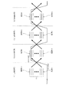
図9に、図6の電源回路50の昇圧回路52、リミッタ回路53の構成例を示す。
FIG. 9 shows a configuration example of the
昇圧回路52は、互いに昇圧能力が異なる複数のチャージポンプ回路を備え、これらのチャージポンプ回路の動作をイネーブル制御することで昇圧能力を変更できるようになっている。
The
例えば、昇圧回路52は、図9に示すように、第1及び第2のチャージポンプ回路1001、1002、切替制御部110を有する。昇圧回路52(電源回路50)の外部接続端子TC1、TC2には、第1のチャージポンプ回路1001のチャージポンプ動作に用いられる第1のフライングコンデンサFC1が接続される。また、昇圧回路52(電源回路50)の外部接続端子TC3、TC4には、第2のチャージポンプ回路1002のチャージポンプ動作に用いられる第2のフライングコンデンサFC2が接続される。
For example, the
第2のフライングコンデンサFC2の容量値は、第1のフライングコンデンサFC1の容量値より大きい。また、第1のチャージポンプ回路1001を構成するトランジスタのサイズ(チャネル長×チャネル幅)は、第2のチャージポンプ回路1002を構成するトランジスタのサイズより小さく、第1のチャージポンプ回路1001を構成するトランジスタの電流駆動能力は、第2のチャージポンプ回路1002を構成するトランジスタの電流駆動能力より小さい。こうすることで、第1のチャージポンプ回路1001の昇圧能力を、第2のチャージポンプ回路1002の昇圧能力より小さくできる。
The capacitance value of the second flying capacitor FC2 is larger than the capacitance value of the first flying capacitor FC1. The size of the transistors constituting the first charge pump circuit 100 1 (channel length × channel width) is smaller than the size of the transistors constituting the second
イネーブル状態に設定された各チャージポンプ回路は、システム接地電源電圧VSSとシステム電源電圧VDDとの間の電圧を、システム接地電源電圧VSSを基準に例えば2倍に昇圧した電源電圧VOUTを生成する。 Each charge pump circuit set in the enabled state generates a power supply voltage VOUT obtained by boosting a voltage between the system ground power supply voltage VSS and the system power supply voltage VDD by, for example, twice the system ground power supply voltage VSS.
切替制御部110は、第1及び第2のチャージポンプ回路1001、1002のイネーブル制御を行う。より具体的には、切替制御部110は、第1及び第2のチャージポンプ回路1001、1002のいずれか1つをイネーブル状態に設定したり、第1及び第2のチャージポンプ回路1001、1002の両方をイネーブル状態に設定したりできる。こうすることで、切替制御部110は、昇圧回路52の昇圧能力を3種類のいずれかから選択して制御できる。
The switching
図10に、図9の第1のチャージポンプ回路1001の構成例の回路図を示す。
FIG. 10 is a circuit diagram showing a configuration example of the first
図10では、第1のチャージポンプ回路1001の構成例について説明するが、第2のチャージポンプ回路1002の構成例についても同様である。
In Figure 10, it will be described first configuration example of the
第1のチャージポンプ回路1001は、チャージポンプ動作により第1のフライングコンデンサFC1に蓄積された電荷を用いて昇圧電圧を生成するためのスイッチ素子であるトランジスタを含む。より具体的には、第1のチャージポンプ回路1001は、昇圧電圧が出力される出力電源線とシステム電源電圧VDDが供給される電源線との間に直列に挿入されるP型(広義には第1導電型)MOSトランジスタ(以下、単にトランジスタ)PT1、PT2を含む。また、第1のチャージポンプ回路1001は、システム電源電圧VDDが供給される電源線とシステム接地電源電圧VSSが供給される電源線との間に直列に挿入されるP型MOSトランジスタPT3、N型(広義には第2導電型)MOSトランジスタ(以下、単にトランジスタ)NT1を含む。
The first
トランジスタPT1のゲートには、チャージクロックCK1Pが供給される。トランジスタPT2のゲートには、チャージクロックCK2Pが供給される。トランジスタPT3のゲートには、チャージクロックCK3Pが供給される。トランジスタNT1のゲートには、チャージクロックCK1Nが供給される。 The charge clock CK1P is supplied to the gate of the transistor PT1. The charge clock CK2P is supplied to the gate of the transistor PT2. The charge clock CK3P is supplied to the gate of the transistor PT3. The charge clock CK1N is supplied to the gate of the transistor NT1.
トランジスタPT1のソースに、昇圧電圧が出力される電源線が接続される。トランジスタPT1、PT2の接続ノードに、端子TC1を介して第1のフライングコンデンサFC1の一端が接続される。トランジスタPT3、NT1の接続ノードに、端末TC2を介して第1のフライングコンデンサFC1の他端が接続される。 A power supply line for outputting a boosted voltage is connected to the source of the transistor PT1. One end of the first flying capacitor FC1 is connected to the connection node of the transistors PT1 and PT2 via the terminal TC1. The other end of the first flying capacitor FC1 is connected to the connection node of the transistors PT3 and NT1 via the terminal TC2.
図11に、図10のチャージクロックCK1P、CK2P、CK3P、CK1Nのタイミングを模式的に示す。 FIG. 11 schematically shows the timing of the charge clocks CK1P, CK2P, CK3P, and CK1N in FIG.
チャージクロックCK1PがLレベルのとき、チャージクロックCK2PがHレベル、チャージクロックCK3P、CK1NがLレベルとなる(期間PH1)。また、チャージクロックCK1PがHレベルのとき、チャージクロックCK2PがHレベル、チャージクロックCK3P、CK1NがHレベルとなる(期間PH2)。 When the charge clock CK1P is at the L level, the charge clock CK2P is at the H level, and the charge clocks CK3P and CK1N are at the L level (period PH1). When the charge clock CK1P is at the H level, the charge clock CK2P is at the H level, and the charge clocks CK3P and CK1N are at the H level (period PH2).
期間PH1では、トランジスタPT1がオン、トランジスタPT2がオフとなり、端子TC1を介して接続される第1のフライングコンデンサFC1の一端の電圧が、出力電源線に出力される。このとき、トランジスタPT3がオン、トランジスタNT1がオフとなり、外部接続端子TC2を介して接続される第1のフライングコンデンサFC1に他端には、システム電源電圧VDDが供給される。 In the period PH1, the transistor PT1 is turned on, the transistor PT2 is turned off, and the voltage at one end of the first flying capacitor FC1 connected via the terminal TC1 is output to the output power supply line. At this time, the transistor PT3 is turned on, the transistor NT1 is turned off, and the system power supply voltage VDD is supplied to the other end of the first flying capacitor FC1 connected via the external connection terminal TC2.
期間PH2では、トランジスタPT1がオフ、トランジスタPT2がオンとなり、端子TC1を介して接続される第1のフライングコンデンサFC1の一端には、システム電源電圧VDDが供給される。このとき、トランジスタPT3がオフ、トランジスタNT1がオンとなるため、外部接続端子TC2を介して接続される第1のフライングコンデンサFC1の他端には、システム接地電源電圧VSSが供給される。従って、期間PH2では、第1のフライングコンデンサFC1には、システム電源電圧VDDとシステム接地電源電圧VSSとの間の電圧に対応した電荷が蓄積される。 In the period PH2, the transistor PT1 is turned off and the transistor PT2 is turned on, and the system power supply voltage VDD is supplied to one end of the first flying capacitor FC1 connected through the terminal TC1. At this time, since the transistor PT3 is turned off and the transistor NT1 is turned on, the system ground power supply voltage VSS is supplied to the other end of the first flying capacitor FC1 connected via the external connection terminal TC2. Therefore, in the period PH2, the first flying capacitor FC1 accumulates charges corresponding to the voltage between the system power supply voltage VDD and the system ground power supply voltage VSS.
そして、再び、期間PH1では、上述のように出力電源線に、第1のフライングコンデンサFC1の一端の電圧が出力される。このとき、外部接続端子TC2に接続される第1のフライングコンデンサFC1の他端の電圧がシステム電源電圧VDDとなるため、出力電源線の電圧は、システム電源電圧VDDとシステム接地電源電圧VSSとの間の電圧の2倍の電圧となる。 In the period PH1, again, the voltage at one end of the first flying capacitor FC1 is output to the output power line as described above. At this time, since the voltage at the other end of the first flying capacitor FC1 connected to the external connection terminal TC2 becomes the system power supply voltage VDD, the voltage of the output power supply line is between the system power supply voltage VDD and the system ground power supply voltage VSS. The voltage is twice the voltage between them.
なお、トランジスタPT1、PT2が同時にオンとならないように、チャージクロックCK1P、CK2Pを変化させることが望ましい。また、トランジスタPT2、PT3が同時にオンとならないように、チャージクロックCK2P、CK3Pを変化させることが望ましい。更に、トランジスタPT3、NT1が同時にオンとならないように、チャージクロックCK3P、CK1Nを変化させることが望ましい。 It is desirable to change the charge clocks CK1P and CK2P so that the transistors PT1 and PT2 are not turned on at the same time. Further, it is desirable to change the charge clocks CK2P and CK3P so that the transistors PT2 and PT3 are not turned on at the same time. Furthermore, it is desirable to change the charge clocks CK3P and CK1N so that the transistors PT3 and NT1 are not turned on at the same time.
図9に戻って説明を続ける。 Returning to FIG. 9, the description will be continued.
図9のリミッタ回路53は、コンパレータCMP1と、電圧制限回路150とを含む。
The
コンパレータCMP1には、電圧VOUTとシステム接地電源電圧VSSとの間の電圧を抵抗分割することにより得られた入力電圧Vinと、所与の基準電圧VREFとが入力される。そして、コンパレータCMP1は、入力電圧Vinと基準電圧VREFとの比較結果を比較結果パルスとして出力する。 The comparator CMP1 receives an input voltage Vin obtained by resistance-dividing the voltage between the voltage VOUT and the system ground power supply voltage VSS and a given reference voltage VREF. Then, the comparator CMP1 outputs the comparison result between the input voltage Vin and the reference voltage VREF as a comparison result pulse.
電圧制限回路150は、P型MOSトランジスタTROにより構成される。P型MOSトランジスタTROのゲートには、コンパレータCMP1からの比較結果パルスが入力される。P型MOSトランジスタTROのソースには、電圧VOUTが供給される電源線が接続される。P型MOSトランジスタTROのドレインには、システム電源電圧VDDが供給される電源線に接続される。
The
図12に、図9のコンパレータCMP1と電圧制限回路150の構成例の回路図を示す。
FIG. 12 shows a circuit diagram of a configuration example of the comparator CMP1 and the
コンパレータCMP1は、差動増幅器DIF1と、出力回路DRV1とを含む。差動増幅器DIF1は、ソースが接続された差動トランジスタ対と、差動トランジスタ対のソースに電流を供給する電流源トランジスタと、差動トランジスタ対を構成する各トランジスタに電流を供給するカレントミラー回路とを含む。差動トランジスタ対を構成するトランジスタのうち、非反転入力端子となるトランジスタのゲートには基準電圧VREFが供給され、反転入力端子となるトランジスタのゲートには入力電圧Vinが供給される。出力回路DRV1は、直列に接続されたP型MOSトランジスタPDRV1と、N型MOSトランジスタNDRV1とを含む。N型MOSトランジスタNDRV1のゲートには、差動増幅器DIF1の電流源トランジスタのゲート電圧と同じ電圧が供給され、P型MOSトランジスタPDRV1のドレインを駆動する。P型MOSトランジスタPDRV1のゲートには、差動増幅器DIF1の出力電圧が供給される。 The comparator CMP1 includes a differential amplifier DIF1 and an output circuit DRV1. The differential amplifier DIF1 includes a differential transistor pair to which a source is connected, a current source transistor that supplies a current to the source of the differential transistor pair, and a current mirror circuit that supplies a current to each transistor constituting the differential transistor pair. Including. Among the transistors constituting the differential transistor pair, the reference voltage VREF is supplied to the gate of the transistor serving as the non-inverting input terminal, and the input voltage Vin is supplied to the gate of the transistor serving as the inverting input terminal. Output circuit DRV1 includes a P-type MOS transistor PDRV1 and an N-type MOS transistor NDRV1 connected in series. The gate of the N-type MOS transistor NDRV1 is supplied with the same voltage as the gate voltage of the current source transistor of the differential amplifier DIF1, and drives the drain of the P-type MOS transistor PDRV1. The output voltage of the differential amplifier DIF1 is supplied to the gate of the P-type MOS transistor PDRV1.
そして、電圧制限回路150を構成するP型MOSトランジスタTROのゲートには、出力回路DRV1のP型MOSトランジスタPDRV1のドレインの電圧が供給される。
The voltage of the drain of the P-type MOS transistor PDRV1 of the output circuit DRV1 is supplied to the gate of the P-type MOS transistor TRO constituting the
従って、入力電圧Vinが基準電圧VREFより高電位の場合、差動増幅器DIF1の出力電圧の電位が上がり、P型MOSトランジスタPDRV1のインピーダンスが上がる。その結果、コンパレータCMP1の出力である比較結果パルスの電位が下がる方向に変化する。このとき、P型MOSトランジスタTROのインピーダンスが下がる方向に変化し、システム電源電圧VDDが供給される電源線に対して放電される電荷量が多くなる。 Therefore, when the input voltage Vin is higher than the reference voltage VREF, the potential of the output voltage of the differential amplifier DIF1 increases and the impedance of the P-type MOS transistor PDRV1 increases. As a result, the potential of the comparison result pulse, which is the output of the comparator CMP1, changes in the direction of decreasing. At this time, the impedance of the P-type MOS transistor TRO changes in a decreasing direction, and the amount of charge discharged to the power supply line to which the system power supply voltage VDD is supplied increases.
一方、入力電圧Vinが基準電圧VREFより低電位の場合、差動増幅器DIF1の出力電圧の電位が下がり、P型MOSトランジスタPDRV1のインピーダンスが下がる。その結果、コンパレータCMP1の出力である比較結果パルスの電位が上がる方向に変化する。このとき、P型MOSトランジスタTROのインピーダンスが上がる方向に変化し、システム電源電圧VDDが供給される電源線に対して放電される電荷量が少なくなる。 On the other hand, when the input voltage Vin is lower than the reference voltage VREF, the potential of the output voltage of the differential amplifier DIF1 decreases and the impedance of the P-type MOS transistor PDRV1 decreases. As a result, the potential of the comparison result pulse, which is the output of the comparator CMP1, changes in the increasing direction. At this time, the impedance of the P-type MOS transistor TRO changes in the increasing direction, and the amount of charge discharged to the power supply line to which the system power supply voltage VDD is supplied decreases.
図13に、コンパレータCMP1の比較結果パルスの説明図を示す。 FIG. 13 is an explanatory diagram of the comparison result pulse of the comparator CMP1.
比較結果パルスは、図13に示すようにパルス信号となる。入力電圧Vinが基準電圧VREFより高電位の場合には、比較結果パルスがLレベルとなり、上述のようにシステム電源電圧VDDが供給される電源線に電荷を放電する期間となる。また、入力電圧Vinが基準電圧VREFより低電位の場合には、比較結果パルスがHレベルとなり、該電源線に電荷を放電しない期間となる。 The comparison result pulse becomes a pulse signal as shown in FIG. When the input voltage Vin is higher than the reference voltage VREF, the comparison result pulse is at the L level, which is a period for discharging charges to the power supply line to which the system power supply voltage VDD is supplied as described above. Further, when the input voltage Vin is lower than the reference voltage VREF, the comparison result pulse is at the H level, and it is a period during which no charge is discharged to the power supply line.
このように、リミッタ回路53では、入力電圧Vinが基準電圧VREFより高電位側になると、P型MOSトランジスタTROがオンとなって、電圧VOUTが供給される電源線の電荷を、システム電源電圧VDDが供給される電源線に放電する制御を行う。
Thus, in the
ところで、本実施形態では、昇圧回路52が、電源回路50の出力負荷に応じて昇圧能力を変更できるようになっている。そのため、本実施形態では、電源回路50が、出力負荷を評価するための評価値である総和データGSUMを所与の閾値と比較することで、昇圧能力を変更するか否かを判断できるようになっている。即ち、電源回路50は、電源回路50の出力負荷に対して昇圧能力が高いと判断されるときには、昇圧能力がより低くなるように該昇圧能力を変更し、出力負荷に対して昇圧能力が低いと判断されるときには、昇圧能力がより高くなるように該昇圧能力を変更する。
By the way, in this embodiment, the
更に、この閾値は、リミッタ回路53が昇圧電圧である電圧VOUTの電位を制限したか否かを示すリミッタ動作情報に基づいて更新される。従って、電源回路50は、電源回路50の出力負荷とリミッタ動作情報とに基づいて、昇圧回路52の昇圧能力を変更することができる。
Further, this threshold value is updated based on limiter operation information indicating whether or not the
このような電源回路50は、図9に示すように、更に、コンパレータCMP2、レベルシフタ180、カウンタ182、判定ロジック部184、閾値更新部186を含むことができる。
As shown in FIG. 9, the
コンパレータCMP2には、リミッタ回路53からの比較結果パルスと、所与の閾値電圧VTHとが入力される。コンパレータCMP2の高電位側の電源を電圧VOUT、低電位側の電源をシステム接地電源電圧VSSとすると、閾値電圧VTHは、次の式で表すことができる。
The comparison result pulse from the
VTH=VOUT−Vthp−α ・・・(1)
ここで、Vthpは、電圧制限回路150を構成するP型MOSトランジスタTROの閾値電圧であり、αは0.1V〜0.2V程度の正の定数値である。このようなコンパレータCMP2の出力信号は、図13の比較結果パルスのHレベル、Lレベルに対応した信号となり、電荷を電源線に放電する時間の長さを監視するための信号となる。
VTH = VOUT−Vthp−α (1)
Here, Vthp is a threshold voltage of the P-type MOS transistor TRO constituting the
レベルシフタ180は、このようなコンパレータCMP2の出力信号の電圧レベルを所与の電圧レベルの信号にシフトする。カウンタ182は、レベルシフタ180の出力信号であるパルス信号のパルス幅又はパルス数をカウントする。カウンタ182の所定期間におけるカウント値を、リミッタ動作情報を示す信号と考えることができる。即ち、昇圧能力が大きいときは、リミッタ回路53が動作している期間が長くなる。そのため、パルス信号のパルス幅又はパルス数をカウントすることで、リミッタ回路53のリミッタ動作情報を数値化できる。パルス信号のパルス数をカウントする場合、例えば一定期間(1又は複数の水平走査期間、1又は複数の垂直走査期間)にリミッタ回路53が動作した期間に対応するパルス数を、ドットクロック(ピクセルクロック)等の所与のクロック信号を用いてカウントすればよい。
The
判定ロジック部184は、総和データGSUMと所与の閾値とを比較することで、昇圧回路52の切替制御部110の制御を行う。本実施形態では、判定ロジック部184からの判定結果に基づいて、切替制御部110が、第1及び第2のチャージポンプ回路1001、1002のうち少なくとも1つがイネーブル状態となるように制御する。この結果、切替制御部110が、昇圧回路52の昇圧能力の変更後に、第1のチャージポンプ回路1001により生成された昇圧電圧、第2のチャージポンプ回路1002により生成された昇圧電圧、又は第1及び第2のチャージポンプ回路1001、1002により生成された昇圧電圧を出力する。
The
更に判定ロジック部184は、カウンタ182のカウント値に基づいて、閾値を更新すべきか否かを判定する。例えば、判定ロジック部184は、所与の更新判定用閾値とカウント値とを比較する。判定ロジック部184によって閾値を更新すべきと判定されたとき、閾値更新部186は現在の閾値をインクリメント又はデクリメントして閾値を更新し、判定ロジック部184に該閾値を供給する。そして、判定ロジック部184は、該閾値と総和データGSUMとを比較することで、切替制御部110の制御を行う。このように、カウント値に基づいてリミッタ回路53の動作期間が長いか短いかを判定することで、閾値が、所与の閾値電圧と電圧VOUT(昇圧電圧)との比較結果に基づいて更新される。
Further, the
図14に、図13の判定ロジック部184の動作の一例の説明図を示す。
FIG. 14 is an explanatory diagram showing an example of the operation of the
本実施形態では、総和データGSUMの最大値に対して、演算対象の走査ラインの総和データGSUMに応じて、昇圧回路52の昇圧能力を変更する。そのため、判定ロジック部184は、2つの閾値THA、THBを有する。閾値THAは、第2のチャージポンプ回路1002をイネーブル状態に設定した状態で、第1のチャージポンプ回路1001をイネーブル状態に設定するか否かを判定するための閾値である。閾値THBは、第1及び第2のチャージポンプ回路1001、1002のいずれかをイネーブル状態に設定するか否かを判定するための閾値である。
In the present embodiment, the boosting capability of the
従って、総和データGSUMが閾値THAより大きいとき、第1及び第2のチャージポンプ回路1001、1002をイネーブル状態に設定する制御が行われる。また、総和データGSUMが閾値THA以下で、且つ閾値THBより大きいとき、第1のチャージポンプ回路1001をディセーブル状態に設定し、第2のチャージポンプ回路1002をイネーブル状態に設定する制御を行う。更に、総和データGSUMが閾値THB以下のとき、第1のチャージポンプ回路1001をイネーブル状態に設定し、第2のチャージポンプ回路1002をディセーブル状態に設定する制御を行う。
Therefore, when the sum data GSUM is larger than the threshold value THA, control is performed to set the first and second
図15に、図13の判定ロジック部184の構成例の要部の回路図を示す。
FIG. 15 is a circuit diagram of a main part of a configuration example of the
判定ロジック部184は、コンパレータCMP10、CMP11、CMP12、CMP13、最小値最大値判定部MM1、MM2を含む。なお、判定ロジック部184は、複数のフリップフロップDFF1〜DFF6を有し、各フリップフロップは図示しない初期化信号により初期化されるものとする。
The
図15の判定ロジック部184には、水平同期信号LP、総和データGSUM、閾値THA、THB、パルスデータPLSET、PCNT1、PCNT2が入力され、制御信号ENB1、ENB2、INCA、DECA、INCB、DECBを出力する。 15 receives the horizontal synchronization signal LP, the sum data GSUM, threshold values THA, THB, and pulse data PLSET, PCNT1, and PCNT2, and outputs control signals ENB1, ENB2, INCA, DECA, INCB, and DECB. To do.
ここで、パルスデータPLSETは、閾値データである。例えば、コンパレータCMP12は、比較結果パルスに基づいて電圧VOUTが所与の閾値電圧(VTH=5.9V)以下となったことを示す比較結果信号、電圧VOUTが所与の閾値電圧(VTH=6.12V)以上となったことを示す比較結果信号を出力できる。そして、電圧VOUTが所与の閾値電圧(VTH=5.9)以下となったことを示す比較結果信号の(所与のレベルを維持する)幅、パルス幅、又は該比較結果信号が所与のレベルを維持する期間を所与のクロック(例えばドットクロック又はピクセルクロック)を用いて検定した結果が、パルスデータPCNT1として入力される。電圧VOUTが所与の閾値電圧(VTH=6.12V)以上となったことを示す比較結果信号の(所与のレベルを維持する)幅、パルス幅、又は該比較結果信号が所与のレベルを維持する期間を所与のクロック(例えばドットクロック又はピクセルクロック)を用いて検定した結果が、パルスデータPCNT2として入力される。パルスデータPLSETと、パルスデータPCNT1、PCNT2の各パルスデータとが比較処理される。
Here, the pulse data PLSET is threshold data. For example, the
昇圧能力が高すぎるとリミッタ回路53が動作することから、パルスデータPCNT1がパルスデータPLSETより大きいと判定されたとき、閾値電圧(VTH=5.9V)に対応する閾値THBをインクリメントする制御を行う。同様に、パルスデータPCNT2がパルスデータPLSETより大きいと判定されたとき、閾値電圧(VTH=6.12V)に対応する閾値THAをインクリメントする制御を行う。
Since the
昇圧能力が低すぎるとリミッタ回路53が動作しないため、パルスデータPCNT1がパルスデータPLSETより小さいと判定されたとき、閾値電圧(VTH=5.9V)に対応する閾値THBをデクリメントする制御を行う。同様に、パルスデータPCNT2がパルスデータPLSETより小さいと判定されたとき、閾値電圧(VTH=6.12V)に対応する閾値THAをデクリメントする制御を行う。
Since the
制御信号INCAは、閾値THAをインクリメントするための制御信号である。制御信号INCBは、閾値THBをインクリメントするための制御信号である。制御信号DECAは、閾値THAをデクリメントするための制御信号である。制御信号DECBは、閾値THBをデクリメントするための制御信号である。 The control signal INCA is a control signal for incrementing the threshold value THA. The control signal INCB is a control signal for incrementing the threshold value THB. The control signal DECA is a control signal for decrementing the threshold value THA. The control signal DECB is a control signal for decrementing the threshold value THB.
制御信号ENB1は、第1のチャージポンプ回路1001をイネーブル状態に設定するための制御信号である。制御信号ENB2は、第2のチャージポンプ回路1002をイネーブル状態に設定するための制御信号である。
The control signal ENB1 is a control signal for setting the first
図15において、コンパレータCMP10は、総和データGSUMが閾値THAより大きいとき、出力信号がHレベルとなる。コンパレータCMP11は、総和データGSUMが閾値THBAより大きいとき、出力信号がHレベルとなる。コンパレータCMP12は、パルスデータPCNT2がパルスデータPLSETより大きいとき、出力信号がHレベルとなる。コンパレータCMP13は、パルスデータPCNT1がパルスデータPLSETより大きいとき、出力信号がHレベルとなる。 In FIG. 15, the comparator CMP10 has an output signal at the H level when the total data GSUM is larger than the threshold value THA. When the sum data GSUM is larger than the threshold value THBA, the output signal of the comparator CMP11 becomes H level. When the pulse data PCNT2 is larger than the pulse data PLSET, the output signal of the comparator CMP12 becomes H level. When the pulse data PCNT1 is larger than the pulse data PLSET, the output signal of the comparator CMP13 becomes H level.
最小値最大値判定部MM1は、閾値THAの各ビットが「1」のときインクリメント制御を禁止するための制御信号を出力する。最小値最大値判定部MM1は、閾値THAの各ビットが「0」のときデクリメント制御を禁止するための制御信号を出力する。 The minimum value / maximum value determination unit MM1 outputs a control signal for prohibiting the increment control when each bit of the threshold value THA is “1”. The minimum value / maximum value determination unit MM1 outputs a control signal for prohibiting decrement control when each bit of the threshold value THA is “0”.
最小値最大値判定部MM2は、閾値THBの各ビットが「1」のときインクリメント制御を禁止するための制御信号を出力する。最小値最大値判定部MM2は、閾値THBの各ビットが「0」のときデクリメント制御を禁止するための制御信号を出力する。 The minimum / maximum value determination unit MM2 outputs a control signal for prohibiting the increment control when each bit of the threshold value THB is “1”. The minimum / maximum value determination unit MM2 outputs a control signal for prohibiting decrement control when each bit of the threshold value THB is “0”.
このように判定ロジック部184は、総和データGSUM、閾値THA、THBに基づいて、第1及び第2のチャージポンプ回路1001、1002をイネーブル状態に設定する制御を行うことができる。また、判定ロジック部184は、比較結果パルスに基づいてリミッタ回路53が動作した期間を判定し、その判定結果に応じて閾値THA、THBをインクリメント又はデクリメントする制御を行うことができる。
As described above, the
以上説明したように、本実施形態によれば、昇圧した電圧がターゲット電圧を超過した場合であっても、昇圧元の電源であるシステム電源電圧VDDが供給される電源線に電荷を放電するようにしたので、システム接地電源電圧VSSが供給される電源線に電荷を放電するよりも大幅に低消費電力化を実現できる。更に、本実施形態によれば、出力負荷に応じて昇圧回路の昇圧能力を変更できるようにしたので、出力負荷が高い場合でも昇圧能力を低下させることなく、且つ出力負荷に対して昇圧効率が低下することを防止できるようになる。 As described above, according to the present embodiment, even when the boosted voltage exceeds the target voltage, the electric charge is discharged to the power supply line to which the system power supply voltage VDD that is the power source of the boost is supplied. Therefore, the power consumption can be significantly reduced compared with the case where electric charges are discharged to the power supply line to which the system ground power supply voltage VSS is supplied. Furthermore, according to the present embodiment, since the boosting capability of the booster circuit can be changed according to the output load, the boosting efficiency can be improved with respect to the output load without reducing the boosting capability even when the output load is high. It becomes possible to prevent the decrease.
3. 電子機器
図16に、本実施形態の電源回路が適用される電子機器の構成例のブロック図を示す。ここでは、電子機器として、携帯電話機の構成例のブロック図を示す。
3. Electronic Device FIG. 16 shows a block diagram of a configuration example of an electronic device to which the power supply circuit of the present embodiment is applied. Here, a block diagram of a configuration example of a mobile phone is shown as an electronic device.
携帯電話機900は、カメラモジュール910を含む。カメラモジュール910は、CCDカメラを含み、CCDカメラで撮像した画像のデータを、YUVフォーマットで表示コントローラ540に供給する。表示コントローラ540は、図1又は図2の表示コントローラ40の機能を有する。
The
携帯電話機900は、表示パネル512を含む。表示パネル512は、ソースドライバ520及びゲートドライバ530によって駆動される。表示パネル512は、複数のゲート線、複数のソース線、複数の画素を含む。表示パネル512は、図1又は図2の表示パネル12の機能を有する。
The
表示コントローラ540は、ソースドライバ520及びゲートドライバ530に接続され、ソースドライバ520に対してRGBフォーマットの階調データを供給する。
The
電源回路542は、ソースドライバ520及びゲートドライバ530に接続され、各ドライバに対して、駆動用の電源電圧を供給する。電源回路542は、図1又は図2の電源回路50の機能を有する。表示ドライバ544としてソースドライバ520、ゲートドライバ530及び電源回路542を含み、該表示ドライバ544が表示パネル512を駆動できる。
The
ホスト940は、表示コントローラ540に接続される。ホスト940は、表示コントローラ540を制御する。またホスト940は、アンテナ960を介して受信された階調データを、変復調部950で復調した後、表示コントローラ540に供給できる。表示コントローラ540は、この階調データに基づき、ソースドライバ520及びゲートドライバ530により表示パネル512に表示させる。ソースドライバ520は、第1〜第3の実施形態のいずれかのソースドライバの機能を有する。ゲートドライバ530は、図1又は図2のゲートドライバ30の機能を有する。
The
ホスト940は、カメラモジュール910で生成された階調データを変復調部950で変調した後、アンテナ960を介して他の通信装置への送信を指示できる。
The
ホスト940は、操作入力部970からの操作情報に基づいて階調データの送受信処理、カメラモジュール910の撮像、表示パネル512の表示処理を行う。
The
なお、本発明は上述した実施の形態に限定されるものではなく、本発明の要旨の範囲内で種々の変形実施が可能である。例えば、本発明は上述の液晶表示パネルの駆動に適用されるものに限らず、エレクトロクミネッセンス、プラズマディスプレイ装置の駆動に適用可能である。更に、表示パネルの駆動に限らず、種々の回路に電源を供給するものに適用可能である。 The present invention is not limited to the above-described embodiment, and various modifications can be made within the scope of the gist of the present invention. For example, the present invention is not limited to being applied to driving the above-described liquid crystal display panel, but can be applied to driving electroluminescence and plasma display devices. Furthermore, the present invention is not limited to driving a display panel, and can be applied to a device that supplies power to various circuits.
更に、上述した実施形態の液晶表示装置は、携帯電話機、携帯型情報機器(PDA等)、デジタルカメラ、プロジェクタ、携帯型オーディオプレーヤ、マスストレージデバイス、ビデオカメラ、電子手帳又はGPS(Global Positioning System)などの種々の電子機器に組み込むことができる。 Furthermore, the liquid crystal display device of the above-described embodiment includes a mobile phone, a portable information device (PDA, etc.), a digital camera, a projector, a portable audio player, a mass storage device, a video camera, an electronic notebook, or a GPS (Global Positioning System). It can be incorporated in various electronic devices.
また、本発明のうち従属請求項に係る発明においては、従属先の請求項の構成要件の一部を省略する構成とすることもできる。また、本発明の1の独立請求項に係る発明の要部を、他の独立請求項に従属させることもできる。 In the invention according to the dependent claims of the present invention, a part of the constituent features of the dependent claims can be omitted. Moreover, the principal part of the invention according to one independent claim of the present invention can be made dependent on another independent claim.
10 液晶表示装置、 12 表示パネル、 20 ソースドライバ、
22、32 シフトレジスタ、 24、26 ラインラッチ、
25 階調データ総和演算部、 27 基準電圧発生回路、 28 DAC、
29 ソース線駆動回路、 30 ゲートドライバ、 34、180 レベルシフタ、
36 出力バッファ、 40 表示コントローラ、 50 電源回路、
52 昇圧回路、 53 リミッタ回路、 54 走査電圧生成回路、
56 対向電極電圧生成回路、 60 表示ドライバ、
1001 第1のチャージポンプ回路、 1002 第2のチャージポンプ回路、
110 切替制御部、 150 電圧制限回路、 182 カウンタ、
184 判定ロジック部、 186 閾値更新部、
CMP1、CMP2 コンパレータ、 FC1 第1のフライングコンデンサ、
FC2 第2のフライングコンデンサ、 G1〜GM、GK ゲート線、
GSUM 総和データ、 S1〜SN、SL ソース線、
TC1〜TC4 外部接続端子、 VTH 閾値電圧、 VREF 基準電圧、
VDD システム電源電圧、 VSS システム接地電源電圧
10 liquid crystal display device, 12 display panel, 20 source driver,
22, 32 shift register, 24, 26 line latch,
25 gradation data sum calculation unit, 27 reference voltage generation circuit, 28 DAC,
29 source line drive circuit, 30 gate driver, 34, 180 level shifter,
36 output buffer, 40 display controller, 50 power supply circuit,
52 booster circuit, 53 limiter circuit, 54 scan voltage generation circuit,
56 counter electrode voltage generation circuit, 60 display driver,
100 1 1st charge pump circuit, 100 2 2nd charge pump circuit,
110 switching control unit, 150 voltage limiting circuit, 182 counter,
184 decision logic unit, 186 threshold update unit,
CMP1, CMP2 comparator, FC1 first flying capacitor,
FC2 second flying capacitors, G 1 ~G M, G K gate lines,
GSUM total data, S 1 to S N , S L source line,
TC1 to TC4 external connection terminal, VTH threshold voltage, VREF reference voltage,
VDD System power supply voltage, VSS System ground power supply voltage
Claims (14)
第1の電圧を基準に第2の電圧を昇圧した昇圧電圧を生成する昇圧回路と、
前記昇圧電圧の電位を制限するリミッタ回路とを含み、
前記リミッタ回路が、
前記昇圧電圧が所与のターゲット電圧になるように前記第2の電圧が供給される電源線に電荷を放電、又は該電源線から電荷を充電し、
前記昇圧回路が、
前記電源回路の出力負荷と、前記リミッタ回路が前記昇圧電圧の電位を制限したか否かを示すリミッタ動作情報とに基づいて、前記昇圧回路の電流駆動能力である昇圧能力を変更することを特徴とする電源回路。 A power supply circuit for outputting a boosted voltage,
A booster circuit that generates a boosted voltage obtained by boosting the second voltage with reference to the first voltage;
A limiter circuit for limiting the potential of the boosted voltage,
The limiter circuit is
Discharging the charge to the power supply line to which the second voltage is supplied so that the boosted voltage becomes a given target voltage, or charging the charge from the power supply line,
The booster circuit is
The boosting capability, which is the current driving capability of the booster circuit, is changed based on the output load of the power supply circuit and limiter operation information indicating whether the limiter circuit has limited the potential of the boosted voltage. Power supply circuit.
前記出力負荷に対して前記昇圧能力が高いと判断されるときには、昇圧能力がより低くなるように該昇圧能力を変更し、
前記出力負荷に対して前記昇圧能力が低いと判断されるときには、昇圧能力がより高くなるように該昇圧能力を変更することを特徴とする電源回路。 In claim 1,
When it is determined that the boost capability is high with respect to the output load, the boost capability is changed so that the boost capability becomes lower,
When it is determined that the boost capability is low with respect to the output load, the boost capability is changed so that the boost capability becomes higher.
前記昇圧回路が、
前記リミッタ動作情報に基づいて更新される閾値と、前記出力負荷との比較結果に応じて、前記昇圧能力を変更することを特徴とする電源回路。 In claim 1 or 2 ,
The booster circuit is
A power supply circuit that changes the boosting capability according to a comparison result between a threshold value updated based on the limiter operation information and the output load.
前記閾値が、
所与の閾値電圧と前記昇圧電圧との比較結果に基づいて更新されることを特徴とする電源回路。 In claim 3 ,
The threshold is
A power supply circuit that is updated based on a comparison result between a given threshold voltage and the boosted voltage.
前記所与の閾値電圧と前記昇圧電圧とを比較するコンパレータと、
前記コンパレータの出力結果のパルス幅又はパルス数をカウントするカウンタとを含み、
前記閾値が、
前記カウンタのカウント数に基づいて更新されることを特徴とする電源回路。 In claim 4 ,
A comparator for comparing the given threshold voltage with the boost voltage;
A counter that counts the pulse width or number of pulses of the output result of the comparator,
The threshold is
The power supply circuit is updated based on a count number of the counter.
電気光学装置の複数のソース線の各ソース線の階調データに対応した駆動電圧が、前記昇圧電圧に基づいて生成される場合に、
前記出力負荷が、
前記複数のソース線の1走査ライン分の階調データの総和に基づいて評価されることを特徴とする電源回路。 In any one of Claims 1 thru | or 5 ,
When a driving voltage corresponding to gradation data of each source line of the plurality of source lines of the electro-optical device is generated based on the boosted voltage,
The output load is
The power supply circuit is evaluated based on a sum of gradation data for one scanning line of the plurality of source lines.
前記昇圧回路が、
第1のフライングコンデンサを用いたチャージポンプ動作により、前記昇圧電圧を生成するための第1のチャージポンプ回路と、
前記第1のフライングコンデンサより容量値の大きい第2のフライングコンデンサを用いたチャージポンプ動作により、前記昇圧電圧を生成するための第2のチャージポンプ回路とを含み、
前記昇圧回路の昇圧能力の変更後に、前記第1のチャージポンプ回路により生成された昇圧電圧、前記第2のチャージポンプ回路により生成された昇圧電圧、又は前記第1及び第2のチャージポンプ回路により生成された昇圧電圧を出力することを特徴とする電源回路。 In any one of Claims 1 thru | or 6 .
The booster circuit is
A first charge pump circuit for generating the boosted voltage by a charge pump operation using a first flying capacitor;
A second charge pump circuit for generating the boosted voltage by a charge pump operation using a second flying capacitor having a larger capacitance value than the first flying capacitor;
After the boosting capability of the booster circuit is changed, the boosted voltage generated by the first charge pump circuit, the boosted voltage generated by the second charge pump circuit, or the first and second charge pump circuits. A power supply circuit that outputs the generated boosted voltage.
請求項1乃至7のいずれか記載の電源回路と、
前記電気光学装置を駆動するための駆動部とを含み、
前記昇圧電圧に基づいて、前記駆動部の駆動電圧を生成することを特徴とする表示ドライバ。 A display driver for driving an electro-optical device,
A power supply circuit according to any one of claims 1 to 7 ,
A drive unit for driving the electro-optical device,
A display driver that generates a drive voltage of the drive unit based on the boosted voltage.
前記駆動部が、
前記昇圧電圧を用いて生成された、階調データに対応した駆動電圧により前記電気光学装置の複数のソース線を駆動することを特徴とする表示ドライバ。 In claim 8 ,
The drive unit is
A display driver, wherein a plurality of source lines of the electro-optical device are driven by a driving voltage corresponding to gradation data generated using the boosted voltage.
複数のソース線と、
前記複数のゲート線を走査するゲートドライバと、
前記複数のソース線を駆動するソースドライバと、
請求項1乃至7のいずれか記載の電源回路とを含み、
前記ゲートドライバの走査電圧及び前記ソースドライバの駆動電圧のうち少なくとも1つが、前記昇圧電圧に基づいて生成されることを特徴とする電気光学装置。 Multiple gate lines,
Multiple source lines,
A gate driver that scans the plurality of gate lines;
A source driver for driving the plurality of source lines;
A power supply circuit according to any one of claims 1 to 7 ,
An electro-optical device, wherein at least one of a scanning voltage of the gate driver and a driving voltage of the source driver is generated based on the boosted voltage.
複数のソース線と、
前記複数のゲート線を走査するゲートドライバと、
前記複数のソース線を駆動する請求項9記載の表示ドライバとを含むことを特徴とする電気光学装置。 Multiple gate lines,
Multiple source lines,
A gate driver that scans the plurality of gate lines;
10. An electro-optical device comprising: the display driver according to claim 9 that drives the plurality of source lines.
Priority Applications (2)
| Application Number | Priority Date | Filing Date | Title |
|---|---|---|---|
| JP2007327194A JP5233272B2 (en) | 2007-01-29 | 2007-12-19 | Power supply circuit, display driver, electro-optical device, and electronic device |
| US12/010,503 US7733160B2 (en) | 2007-01-29 | 2008-01-25 | Power supply circuit, display driver, electro-optical device, and electronic instrument |
Applications Claiming Priority (3)
| Application Number | Priority Date | Filing Date | Title |
|---|---|---|---|
| JP2007017909 | 2007-01-29 | ||
| JP2007017909 | 2007-01-29 | ||
| JP2007327194A JP5233272B2 (en) | 2007-01-29 | 2007-12-19 | Power supply circuit, display driver, electro-optical device, and electronic device |
Publications (3)
| Publication Number | Publication Date |
|---|---|
| JP2008211963A JP2008211963A (en) | 2008-09-11 |
| JP2008211963A5 JP2008211963A5 (en) | 2011-02-10 |
| JP5233272B2 true JP5233272B2 (en) | 2013-07-10 |
Family
ID=39787784
Family Applications (1)
| Application Number | Title | Priority Date | Filing Date |
|---|---|---|---|
| JP2007327194A Active JP5233272B2 (en) | 2007-01-29 | 2007-12-19 | Power supply circuit, display driver, electro-optical device, and electronic device |
Country Status (1)
| Country | Link |
|---|---|
| JP (1) | JP5233272B2 (en) |
Families Citing this family (3)
| Publication number | Priority date | Publication date | Assignee | Title |
|---|---|---|---|---|
| JP5217412B2 (en) * | 2007-01-29 | 2013-06-19 | セイコーエプソン株式会社 | Power supply circuit, display driver, electro-optical device, and electronic device |
| KR101625935B1 (en) * | 2010-01-05 | 2016-05-31 | 삼성전자주식회사 | Charge pump circuit and apparatuses having the same |
| US10755622B2 (en) * | 2016-08-19 | 2020-08-25 | Samsung Electronics Co., Ltd. | Display driver integrated circuit for supporting low power mode of display panel |
Family Cites Families (14)
| Publication number | Priority date | Publication date | Assignee | Title |
|---|---|---|---|---|
| JP2609330B2 (en) * | 1989-08-17 | 1997-05-14 | 富士通株式会社 | Power supply |
| JP2806717B2 (en) * | 1992-10-28 | 1998-09-30 | 日本電気アイシーマイコンシステム株式会社 | Charge pump circuit |
| JP2738335B2 (en) * | 1995-04-20 | 1998-04-08 | 日本電気株式会社 | Boost circuit |
| JPH09312095A (en) * | 1996-05-23 | 1997-12-02 | Toshiba Corp | Semiconductor integrated circuit |
| JP2000102244A (en) * | 1998-07-22 | 2000-04-07 | Ricoh Co Ltd | Dc-to-dc converter |
| JP4109831B2 (en) * | 2001-01-15 | 2008-07-02 | 株式会社東芝 | Semiconductor device |
| JP2003070236A (en) * | 2001-08-23 | 2003-03-07 | Iwate Toshiba Electronics Co Ltd | Semiconductor integrated circuit |
| JP4222768B2 (en) * | 2002-03-27 | 2009-02-12 | 三洋電機株式会社 | Booster and imaging device using the same |
| JP4150614B2 (en) * | 2003-03-10 | 2008-09-17 | 株式会社ケンウッド | Regulator circuit and power supply device |
| JP3759134B2 (en) * | 2003-08-29 | 2006-03-22 | ローム株式会社 | Power supply |
| JP4077429B2 (en) * | 2004-06-09 | 2008-04-16 | 株式会社東芝 | Booster circuit |
| JP2006050778A (en) * | 2004-08-04 | 2006-02-16 | Sanyo Electric Co Ltd | Charge pump circuit |
| JP4096943B2 (en) * | 2004-12-21 | 2008-06-04 | セイコーエプソン株式会社 | Power supply circuit, display driver, electro-optical device, electronic apparatus, and control method for power supply circuit |
| JP5217412B2 (en) * | 2007-01-29 | 2013-06-19 | セイコーエプソン株式会社 | Power supply circuit, display driver, electro-optical device, and electronic device |
-
2007
- 2007-12-19 JP JP2007327194A patent/JP5233272B2/en active Active
Also Published As
| Publication number | Publication date |
|---|---|
| JP2008211963A (en) | 2008-09-11 |
Similar Documents
| Publication | Publication Date | Title |
|---|---|---|
| US7733160B2 (en) | Power supply circuit, display driver, electro-optical device, and electronic instrument | |
| US8125432B2 (en) | Common voltage generation circuit employing a charge-pump operation to generate low-potential-side voltage | |
| US7079127B2 (en) | Reference voltage generation circuit, display driver circuit, display device, and method of generating reference voltage | |
| JP4826383B2 (en) | Power supply circuit, display driver, electro-optical device, and electronic device | |
| US8144090B2 (en) | Driver circuit, electro-optical device, and electronic instrument | |
| US7609256B2 (en) | Power supply circuit, display driver, electro-optical device, electronic instrument, and method of controlling power supply circuit | |
| US20060158413A1 (en) | Power supply circuit, display driver, electro-optical device, electronic instrument, and method of controlling power supply circuit | |
| JP2007060732A (en) | Display | |
| JP4093231B2 (en) | Power supply circuit, display driver, electro-optical device, electronic apparatus, and control method for power supply circuit | |
| JP5217412B2 (en) | Power supply circuit, display driver, electro-optical device, and electronic device | |
| US20080084408A1 (en) | Gate driver, electro-optical device, electronic instrument, and drive method | |
| US20070176675A1 (en) | Differential amplifier and digital-to-analog converter | |
| JP4543964B2 (en) | Common voltage generation circuit, power supply circuit, display driver, and display device | |
| JP4229157B2 (en) | Drive circuit, electro-optical device, and electronic apparatus | |
| JP5233272B2 (en) | Power supply circuit, display driver, electro-optical device, and electronic device | |
| US7796125B2 (en) | Voltage supply circuit, power supply circuit, display driver, electro-optic device, and electronic apparatus | |
| US9621035B2 (en) | Control circuit for switching regulator, integrated circuit device, switching regulator, and electronic device | |
| JP2008083286A (en) | Load measuring instrument, drive circuit, electro-optical device, and electronic apparatus | |
| JP4858250B2 (en) | Common voltage generation circuit, power supply circuit, display driver, and common voltage generation method | |
| US20100225676A1 (en) | Integrated circuit device, electro optical device and electronic apparatus | |
| JP4229158B2 (en) | Drive circuit, electro-optical device, and electronic apparatus | |
| JP4492679B2 (en) | Power supply circuit, display driver, electro-optical device, and electronic device | |
| JP2007114682A (en) | Counter electrode voltage generation circuit, power source circuit, electrooptical apparatus, and electronic equipment | |
| JP2007114559A (en) | Counter electrode voltage generation circuit, power source circuit, electrooptical apparatus, and electronic equipment | |
| JP2006178073A (en) | Power supply circuit, display driver, electro-optical device, electronic equipment and control method of the power supply circuit |
Legal Events
| Date | Code | Title | Description |
|---|---|---|---|
| A521 | Written amendment |
Free format text: JAPANESE INTERMEDIATE CODE: A523 Effective date: 20101216 |
|
| A621 | Written request for application examination |
Free format text: JAPANESE INTERMEDIATE CODE: A621 Effective date: 20101216 |
|
| A977 | Report on retrieval |
Free format text: JAPANESE INTERMEDIATE CODE: A971007 Effective date: 20120724 |
|
| A131 | Notification of reasons for refusal |
Free format text: JAPANESE INTERMEDIATE CODE: A131 Effective date: 20120821 |
|
| A521 | Written amendment |
Free format text: JAPANESE INTERMEDIATE CODE: A523 Effective date: 20121022 |
|
| TRDD | Decision of grant or rejection written | ||
| A01 | Written decision to grant a patent or to grant a registration (utility model) |
Free format text: JAPANESE INTERMEDIATE CODE: A01 Effective date: 20130226 |
|
| A61 | First payment of annual fees (during grant procedure) |
Free format text: JAPANESE INTERMEDIATE CODE: A61 Effective date: 20130311 |
|
| R150 | Certificate of patent or registration of utility model |
Free format text: JAPANESE INTERMEDIATE CODE: R150 Ref document number: 5233272 Country of ref document: JP Free format text: JAPANESE INTERMEDIATE CODE: R150 |
|
| FPAY | Renewal fee payment (event date is renewal date of database) |
Free format text: PAYMENT UNTIL: 20160405 Year of fee payment: 3 |
|
| S531 | Written request for registration of change of domicile |
Free format text: JAPANESE INTERMEDIATE CODE: R313531 |
|
| R350 | Written notification of registration of transfer |
Free format text: JAPANESE INTERMEDIATE CODE: R350 |