JP5225734B2 - Multilayer wiring board - Google Patents
Multilayer wiring board Download PDFInfo
- Publication number
- JP5225734B2 JP5225734B2 JP2008108890A JP2008108890A JP5225734B2 JP 5225734 B2 JP5225734 B2 JP 5225734B2 JP 2008108890 A JP2008108890 A JP 2008108890A JP 2008108890 A JP2008108890 A JP 2008108890A JP 5225734 B2 JP5225734 B2 JP 5225734B2
- Authority
- JP
- Japan
- Prior art keywords
- layer
- layers
- fiber bundle
- resin base
- substrate
- Prior art date
- Legal status (The legal status is an assumption and is not a legal conclusion. Google has not performed a legal analysis and makes no representation as to the accuracy of the status listed.)
- Expired - Fee Related
Links
Images
Landscapes
- Production Of Multi-Layered Print Wiring Board (AREA)
Description
本発明は、2層以上の配線層を備えた全層ビルドアップ構造の多層配線基板に関する。 The present invention relates to a multilayer wiring board having an all-layer buildup structure including two or more wiring layers.
全層ビルドアップ構造の多層配線基板は、複雑な電子回路を高密度に構成し、その上に種々の電子部品を高密度に実装することを目的として開発された電子機器用部材である。この全層ビルドアップ構造の多層配線基板は、銅配線と樹脂で構成される複数の配線層と、樹脂と繊維束で構成される複数の樹脂基材層とを交互に重ね合わせた構造を有し、様々なデジタル機器やモバイル機器に用いられている。 A multilayer wiring board having an all-layer build-up structure is a member for electronic equipment developed for the purpose of constructing a complicated electronic circuit with a high density and mounting various electronic components on the electronic circuit. This multilayer wiring board having a full-layer build-up structure has a structure in which a plurality of wiring layers composed of copper wiring and resin and a plurality of resin base layers composed of resin and fiber bundles are alternately stacked. It is used in various digital devices and mobile devices.
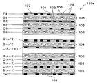
最初に、一般的な全層ビルドアップ構造の多層配線基板について説明する。図9に全層ビルドアップ構造の多層配線基板(場合により「基板」と略す)の基本的な構成を示す。基板100aは、n層(nは3以上の整数)の配線層(C1〜Cn)と(n−1)層の樹脂基材層[B1〜B(n−1)]とが、交互に重なり合う状態で積層されている。以降、配線層および樹脂基材層を総称する場合には、それぞれ配線層Cおよび樹脂基材層Bと表示する。
First, a general multilayer wiring board having a full-layer buildup structure will be described. FIG. 9 shows a basic configuration of a multilayer wiring board (sometimes abbreviated as “substrate”) having an all-layer build-up structure. In the
配線層Cは銅配線101と絶縁性の樹脂103で構成されている。樹脂基材層Bは、織布状もしくは不織布状の繊維束102に絶縁性の樹脂103が含浸されて構成されている。なお、図では、樹脂基材層Bとして、繊維束102に樹脂103が含浸された状態を模式的に表している。以後の図面においても同様に表示する。
The wiring layer C is composed of a
繊維束102としては、一般にガラス繊維やアラミド繊維が用いられる。また、絶縁性の樹脂103としては、エポキシ樹脂、フェノール樹脂、ポリイミド、BT樹脂等の熱硬化性の樹脂が用いられる。
As the
通常、配線層Cおよび樹脂基材層Bは、絶縁性の樹脂が含浸された繊維束と配線パターンが形成された銅箔とを重ねた状態で加圧・加熱して樹脂を硬化させることにより形成される。配線層Cを構成する樹脂103は、加圧・加熱の際に、繊維束に含浸された樹脂の一部が配線パターンの間に入り込むことにより形成される。
Usually, the wiring layer C and the resin base material layer B are formed by pressurizing and heating the fiber bundle impregnated with the insulating resin and the copper foil on which the wiring pattern is formed, to cure the resin. It is formed. The
なお、図には示されていないが、各配線層Cの間は、樹脂基材層Bに形成されたビアホールもしくはスルーホールによって電気的に接続されている。また上記した全層ビルドアップ構造の多層配線基板の構成については、非特許文献1に詳しく定義されている(第2頁の構造例3、4参照)。 Although not shown in the figure, the wiring layers C are electrically connected by via holes or through holes formed in the resin base layer B. Further, the configuration of the multilayer wiring board having the above-described all-layer buildup structure is defined in detail in Non-Patent Document 1 (see Structure Examples 3 and 4 on the second page).
樹脂基材層Bは、基板製造時の積層プレス工程において多層構造の中央層となるコア基材層104と、コア基材層104の上下に積層される積層基材層105とに分けられる。コア基材層104および積層基材層105を構成する樹脂基材については、同一の場合と異なる場合がある。これに対し、積層基材層105の各層の樹脂基材については、繊維束の含有率が一定である単一の材料が用いられる。
The resin base material layer B is divided into a core
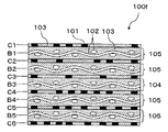
基板100aは、リフローはんだ付け工程において、表裏の実装面に電子部品が仮止めされた状態でリフローベルトあるいはリフローパレット上に配置され、常温から220℃以上に昇温してはんだ付けされた後、再び常温に降温される。このとき基板100aには、残銅率(配線層Cの全体の面積に占める銅配線の面積の比率)が各配線層間において異なることによって配線層間の熱膨張量に差が生じ、そのことに起因して反りが生じる。基板の反りが生じるメカニズムを、図10を参照しながら具体的に説明する。
In the reflow soldering process, the
図10に示す基板100fは、上部から順にC1〜C6までの6層の配線層を有し、各配線層の間に、上部から順にB1、B2(ともに積層基材層105)、B3(コア基材層104)、B4、B5(ともに積層基材層105)の5層の樹脂基材層を有する。各配線層の残銅率は配線層C1から順に、32%、28%、37%、46%、52%、54%である。この場合、コア基材層104(樹脂基材層B3)を境にした上側の各配線層(C1〜C3)と下側の各配線層(C4〜C6)の残銅率の平均値を出すと、残銅率の平均値はコア基材層104の下側の方が大きい。
A
配線層Cを構成する銅配線101と樹脂103とを比較すると、樹脂103の方が銅配線101より線膨張係数が大きい。このため、残銅率が大きい配線層は温度負荷による熱膨張量が小さくなる。よって、図10に示す基板100fにおいては、コア基材層104を境にした上側の熱膨張量が大きく、下側の熱膨張量が小さい。したがって、温度を負荷した場合、基板は上側に凸に反る。
When the
リフローはんだ付け工程時の基板の反りが生じたままの状態で電子部品を実装すると、電子部品と基板との間の接続信頼性を著しく低下させることとなる。このことは、多層配線基板を組み込んだ電子回路の品質を悪化させる大きな要因となっている。 If the electronic component is mounted in a state where the substrate is warped during the reflow soldering process, the connection reliability between the electronic component and the substrate is significantly reduced. This is a major factor that deteriorates the quality of an electronic circuit incorporating a multilayer wiring board.
リフローはんだ付け工程時の基板の反りを防止するために、従来、特許文献1に示す対策が採られていた。すなわち、前述の図9に示すように、各配線層Cにおいて残銅率の違いに由来する熱膨張量の差ができるだけ生じないようにするため、配線層Cに、電子回路を構成する本来の銅配線101とは別にダミーパターン108を形成し、各配線層Cの残銅率ができる限り一律になるようにしていた。
しかし、電子回路の高密度実装が要求される小型電子機器用の基板では、配線層にダミーパターンを設ける十分なスペースを確保することができず、基板の反りを低減することが困難であった。 However, in a board for a small electronic device that requires high-density mounting of electronic circuits, a sufficient space for providing a dummy pattern in the wiring layer cannot be secured, and it is difficult to reduce the warpage of the board. .
本発明は、上記従来の問題点を解決するもので、配線層にダミーパターンを設けるスペースがない場合でも、反りが低減できる多層配線基板を提供することを目的とする。 SUMMARY OF THE INVENTION An object of the present invention is to solve the above-described conventional problems, and to provide a multilayer wiring board capable of reducing warping even when there is no space for providing a dummy pattern in a wiring layer.
上記目的を達成するために、本発明に係る多層配線基板は、
導電材料からなる配線と絶縁性の樹脂で構成されたn(nは4以上の整数)層の配線層と、繊維束に絶縁性の樹脂が含浸された(n−1)層の樹脂基材層とが、交互に重なり合う状態で積層された多層配線基板であって、
前記配線層間の熱膨張量の差を打ち消すように、
前記(n−1)層の樹脂基材層は、そのうちの1つの層と、それ以外の他の層との2種類の層があり、
前記1つの層と、前記他の層とは、層厚、並びに、前記繊維束の種類および太さは互いに同じであるが、前記1つの層だけが前記繊維束の間隔が前記他の層の前記繊維束の間隔と異なり、これにより、前記1つの層の繊維束含有率だけが、前記他の層の繊維束含有率と異なり、前記他の層の繊維含有率は互いに差異がない、多層配線基板である。ここで、前記1つの層に、色素を加えて、前記他の層と見分けがつくようにするのも好ましい。
In order to achieve the above object, a multilayer wiring board according to the present invention comprises:
Wiring made of conductive material and n (n is an integer of 4 or more) wiring layer composed of insulating resin, and (n-1) layer resin base material in which fiber bundle is impregnated with insulating resin A multilayer wiring board in which layers are laminated in an alternately overlapping state,
To negate the difference in thermal expansion between the wiring layers,
The (n-1) layer resin substrate layer includes a layer of one of its, there are two types of layers and the other other layer,
The one layer and the other layer have the same layer thickness and the same type and thickness of the fiber bundle, but only the one layer has the fiber bundle interval of the other layer. Unlike the spacing of the fiber bundles, thereby, the only fiber bundle content of one layer, the different from the fiber bundle content of the other layers, the fiber content of the other layers differences have greens each other, the multi-layer It is a wiring board. Here, it is also preferable to add a pigment to the one layer so that it can be distinguished from the other layers.
ここで、nが偶数の場合、
n/2番目の前記樹脂基材層を境として、一方の実装面から数えて1番目から(n/2)番目までの前記配線層の残銅率の平均値が、(n/2+1)番目からn番目までの前記配線層の残銅率の平均値より大きく、
1番目から(n/2−1)番目までの前記樹脂基材層のうちの1層が前記1つの層であり、その繊維束含有率が、前記他の層の繊維束含有率よりも小さいことが好ましい。
Here, when n is an even number,
The average value of the remaining copper ratio of the wiring layer from the first to the (n / 2) th, counting from one mounting surface, with the n / 2th resin substrate layer as a boundary, is (n / 2 + 1) th Larger than the average value of the remaining copper ratio of the wiring layer from the first to the nth,
From the first is one layer wherein one layer of said resin base layer up (n / 2-1) th, the fiber bundle content of its is, than the fiber bundle content of the other layers Small is preferable.
そのとき、前記1番目の樹脂基材層が、前記1つの層であることが好ましい。 At that time , it is preferable that the first resin base layer is the one layer .
一方、nが奇数の場合、
(n+1)/2番目の前記配線層を境として、一方の実装面から数えて1番目から(n−1)/2番目までの前記配線層の残銅率の平均値が、(n+3)/2番目からn番目までの前記配線層の残銅率の平均値より大きく、
1番目から(n−1)/2番目までの前記樹脂基材層のうちの1層が前記1つの層であり、その繊維束含有率が、前記他の層の繊維束含有率よりも小さいことが好ましい。
On the other hand, when n is an odd number,
With the (n + 1) / 2th wiring layer as a boundary, the average value of the remaining copper ratio of the wiring layer from the first to (n-1) / 2th from the one mounting surface is (n + 3) / It is larger than the average value of the remaining copper ratio of the wiring layers from the second to the nth,
Is one layer wherein one layer of said resin base layer from the first to (n-1) / 2 th, fiber bundle content of its is, than the fiber bundle content of the other layers Small is preferable.
更に、nが偶数の場合、
n/2番目の前記樹脂基材層を境として、一方の実装面から数えて1番目から(n/2)番目までの前記配線層の残銅率の平均値が、(n/2+1)番目からn番目までの前記配線層の残銅率の平均値より小さく、
1番目から(n/2−1)番目までの前記樹脂基材層のうちの1層が前記1つの層であり、その繊維束含有率が、前記他の層の繊維束含有率よりも大きいことが好ましい。
Furthermore, when n is an even number,
The average value of the remaining copper ratio of the wiring layer from the first to the (n / 2) th, counting from one mounting surface, with the n / 2th resin substrate layer as a boundary, is (n / 2 + 1) th Smaller than the average value of the remaining copper ratio of the wiring layer from the first to the nth,
From the first is one layer wherein one layer of said resin base layer up (n / 2-1) th, the fiber bundle content of its is, than the fiber bundle content of the other layers Larger is preferred.
そのとき、前記1番目の樹脂基材層が、前記1つの層であることが好ましい。 At that time , it is preferable that the first resin base layer is the one layer .
一方、nが奇数の場合、
(n+1)/2番目の前記配線層を境として、一方の実装面から数えて1番目から(n−1)/2番目までの前記配線層の残銅率の平均値が、(n+3)/2番目からn番目までの前記配線層の残銅率の平均値より小さく、
1番目から(n−1)/2番目までの前記樹脂基材層のうちの1層が前記1つの層であり、その繊維束含有率が、前記他の層の繊維束含有率よりも大きいことが好ましい。
On the other hand, when n is an odd number,
With the (n + 1) / 2th wiring layer as a boundary, the average value of the remaining copper ratio of the wiring layer from the first to (n-1) / 2th from the one mounting surface is (n + 3) / Smaller than the average value of the remaining copper ratio of the second to nth wiring layers,
Is one layer wherein one layer of said resin base layer from the first to (n-1) / 2 th, fiber bundle content of its is, than the fiber bundle content of the other layers Larger is preferred.
本発明に係る多層配線基板は、少なくとも1層の樹脂基材層の繊維束含有率を他の樹脂基材層のそれと異ならせている。結果、各樹脂基材層の熱膨張量に差が生じる。従って、各配線層の残銅率が異なることによって生じる配線層間の熱膨張量の差を、樹脂基材層間の熱膨張量の差を利用して打ち消すことにより、リフローはんだ付けにおける基板の反りを低減することができる。 In the multilayer wiring board according to the present invention, the fiber bundle content of at least one resin base layer is different from that of other resin base layers. As a result, a difference occurs in the thermal expansion amount of each resin base material layer. Therefore, the difference in the thermal expansion amount between the wiring layers caused by the difference in the remaining copper ratio of each wiring layer is canceled by utilizing the difference in the thermal expansion amount between the resin base layers, thereby reducing the warpage of the substrate in the reflow soldering. Can be reduced.
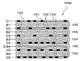
以下、6層の配線層と5層の樹脂基材層を有する基板を例に挙げて、本発明に係る多層配線基板の構成を説明する。図1に、本発明の実施の形態に係る多層配線基板100bの構成を示す。基板100bは、上部から順にC1〜C6までの6層の配線層を有し、各配線層の間に、上部から順にB1、B2(ともに積層基材層105)、B3(コア基材層104)、B4、B5(ともに積層基材層105)の5層の樹脂基材層を有する。各配線層の残銅率はC1から順に、32%、28%、37%、46%、52%、54%である。残銅率は、基板CAD(Computer Aided Design)のデータに含まれる各配線層Cの残銅率から抽出した。なお、図中、図9および図10に示す基板と同一の構成要素には同一の符号を付し、詳細な説明を省略する。以降の説明においても同様とする。
Hereinafter, the configuration of the multilayer wiring board according to the present invention will be described by taking as an example a board having six wiring layers and five resin base layers. FIG. 1 shows a configuration of a
本実施の形態の具体的な説明に先立ち、基板の反りを低減する原理について説明する。本発明に係る基板では、少なくとも1層の樹脂基材層における繊維束含有率を他の樹脂基材層のそれと異ならせている。樹脂基材層は繊維束含有率によって熱膨張量が異なり、繊維束含有率が大きいほど熱膨張量が小さくなる。従って、各配線層の残銅率が異なることによって生じる配線層間の熱膨張量の差を、繊維束含有率が異なることによって生じる樹脂基材層間の熱膨張量の差により打ち消すことができる。 Prior to specific description of the present embodiment, the principle of reducing the warpage of the substrate will be described. In the substrate according to the present invention, the fiber bundle content in at least one resin base layer is different from that of other resin base layers. The resin base material layer has a different thermal expansion amount depending on the fiber bundle content, and the larger the fiber bundle content, the smaller the thermal expansion amount. Therefore, the difference in the thermal expansion amount between the wiring layers caused by the difference in the remaining copper ratio of each wiring layer can be canceled by the difference in the thermal expansion amount between the resin base layers caused by the different fiber bundle contents.
上述の通り、基板100bの各配線層の残銅率はC1から順に、32%、28%、37%、46%、52%、54%である。コア基材層104を境にした上側の各配線層(C1〜C3)と下側の各配線層(C4〜C6)の残銅率の平均値を出すと、それぞれ32%および51%となり、残銅率の平均値はコア基材層104の下側の方が大きい。
As described above, the remaining copper ratio of each wiring layer of the
前述したように、配線層Cは、残銅率が大きいほど熱膨張量が小さくなる。これに対し樹脂基材層Bは、繊維束含有率が大きいほど熱膨張量が小さくなる。従って、以下のいずれかの方法により、基板100bの反りを低減できる。
(1)コア基材層104の下側の積層基材層105(樹脂基材層B4およびB5)のうち少なくとも1層に、他の積層基材層105の繊維束含有率より繊維束含有率が小さい樹脂基材層を用いる。
(2)コア基材層104の上側の積層基材層105(樹脂基材層B1およびB2)のうち少なくとも1層に、他の積層基材層105の繊維束含有率より繊維束含有率が大きい樹脂基材層を用いる。
As described above, the wiring layer C has a smaller amount of thermal expansion as the remaining copper ratio is larger. In contrast, the resin base layer B has a smaller thermal expansion amount as the fiber bundle content is larger. Therefore, the warp of the
(1) At least one of the laminated substrate layers 105 (resin substrate layers B4 and B5) on the lower side of the
(2) At least one of the laminated substrate layers 105 (resin substrate layers B1 and B2) on the upper side of the
上記のいずれの方法においても、基板の各配線層Cに働く上に凸に反らせる力に対して、各樹脂基材層Bに下に凸に反らせる力を持たせることができ、基板の反り低減に有効である。 In any of the above-described methods, it is possible to give each resin base layer B a force to warp downward, which acts on each wiring layer C of the substrate, and to reduce warping of the substrate. It is effective for.
なお、上述した方法では、繊維束含有率の異なる2種類の樹脂基材層を組み合わせることにより基板100bの反りの低減を図っている。これ以外の方法として、繊維束含有率がそれぞれ異なる樹脂基材層を用いることも考えられる。しかしその場合、基板の製造時に、繊維束含有率の異なる複数種類の樹脂基材層を用意する必要がある。
In the above-described method, the warpage of the
繊維束含有率の異なる樹脂基材層の製造は、例えば織布状の繊維束を製造する場合、隣り合う繊維間の間隔を変えるか、繊維そのものの太さを変えることによって行う。しかし、このような繊維間の間隔や繊維の太さの異なる繊維束を製造することは、基板の製造コストを大幅にアップさせる要因となるため、好ましくない。現実的には、上述したように繊維束含有率の異なる2種類の樹脂基材層を用意し、基板の反りの程度に応じて2種類の樹脂基材層を組み合わせて用いることが好ましい。 For example, when producing a woven fabric fiber bundle, the resin base material layers having different fiber bundle contents are manufactured by changing the interval between adjacent fibers or changing the thickness of the fiber itself. However, it is not preferable to manufacture fiber bundles having different fiber spacings or different fiber thicknesses because this significantly increases the manufacturing cost of the substrate. Actually, it is preferable to prepare two types of resin base material layers having different fiber bundle contents as described above, and use a combination of the two types of resin base layers according to the degree of warpage of the substrate.
以下、本実施の形態に係る基板100bの構成について具体的に説明する。本実施の形態では、5層の樹脂基材層のうちB1、B2、B3、B5には繊維束含有率が75%の基材を用い、B4(図1で※印を付与)のみ繊維束含有率が63%の基材を用いた。
Hereinafter, the configuration of the
最初に、基板100bの製造方法について説明する。まず、繊維束含有率の異なる2種類の樹脂基材層を製造した。繊維束として、断面の長半径25μm、短半径10μmのガラス繊維を布状に編んだものを用い、絶縁性の樹脂としてエポキシ樹脂を用いた。繊維束を製造する際に、繊維を編む間隔を変えて、密度の異なる2種類の繊維束を製造した。
First, a method for manufacturing the
次に、このようにして製造した布状の繊維束に樹脂を含浸させて、繊維束含有率の異なる2種類の樹脂基材層を生成した。なお、繊維束含有率が異なる樹脂基材層を生成する際、樹脂に、絶縁性等に影響を与えない程度の色素を加えて一方の樹脂基材層の色を変えると、見分けが容易となる。結果、繊維束含有率が異なる樹脂基材層が誤った位置に配置される事態を防止でき、生産性の向上に寄与する。 Next, the cloth-like fiber bundles manufactured in this way were impregnated with resin to produce two types of resin base material layers having different fiber bundle contents. In addition, when generating resin base material layers having different fiber bundle contents, if the color of one resin base material layer is changed by adding a dye that does not affect the insulating properties, etc., it is easy to distinguish. Become. As a result, it is possible to prevent a situation where resin base material layers having different fiber bundle contents are arranged at wrong positions, which contributes to improvement in productivity.
次に、このようにして生成した樹脂基材層の所定の位置にレーザ加工等によって孔を開け、その孔にインナービアを形成するため、金属粉と熱硬化性樹脂を混合した導電性樹脂組成物を充填した。次に、一方の面に配線パターンが形成された2枚の離型フィルムで樹脂基材層の両面を覆った後、加圧した状態で加熱し、樹脂を硬化させると共に配線パターンを樹脂基材層に固着した。その後、樹脂基材層から離型フィルムを剥離した。なお、配線パターンの形成については、樹脂基材層の両面を銅箔で覆った後、エッチングによって配線パターンを形成する方法を採用してもよい。 Next, a conductive resin composition in which metal powder and a thermosetting resin are mixed to form a hole by laser processing or the like in a predetermined position of the resin base material layer thus generated and to form an inner via in the hole. The product was filled. Next, after covering both sides of the resin base material layer with two release films having a wiring pattern formed on one side, the resin substrate is heated under pressure to cure the resin and the wiring pattern to the resin base material. Sticked to the layer. Then, the release film was peeled from the resin base material layer. In addition, about formation of a wiring pattern, after covering both surfaces of a resin base material layer with copper foil, you may employ | adopt the method of forming a wiring pattern by an etching.
このようにして得られた1層目の樹脂基材層および配線層の上に繊維束および一方の面に配線パターンが形成された離型フィルムを載せ、上述と同様の方法でインナービアを形成した後、加圧・加熱した。図1に示す順序で繊維束含有率が異なる2種類の樹脂基材層を積み重ねながら、上述の処理を繰り返して行い、最終的に5層の樹脂基材層Bおよび6層の配線層Cを有する基板100bを製造した。
A fiber bundle and a release film having a wiring pattern formed on one surface are placed on the first resin base layer and wiring layer thus obtained, and an inner via is formed in the same manner as described above. Then, pressurization and heating were performed. The above process is repeated while stacking two types of resin base material layers having different fiber bundle contents in the order shown in FIG. 1, and finally five resin base material layers B and six wiring layers C are formed. The board |
製造された基板100bの配線層Cの厚みは約10μm、樹脂基材層Bの厚みは約30μmであった。このようにして製造された基板100bを50mm×50mmの大きさに切り出し、リフロー時の最高温度260℃を負荷したところ、反りは1.21mmであった。
The thickness of the wiring layer C of the manufactured
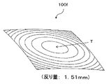
比較例として、図10に示す構成の基板100fを、基板100bと同一の繊維束および樹脂を用いて製造し、50mm×50mmの大きさに切り出した。基板100bと基板100fで異なるのは、樹脂基材層B4の繊維束含有率が基板100bでは63%であるのに対し、基板100fでは他の樹脂基材層と同様に75%である点である。基板100fについてリフロー時の最高温度260℃を負荷したところ、反りは1.51mmであった。
As a comparative example, a
次に、4層の積層基材層105のうち1層の積層基材層(樹脂基材層B1、B2、B4およびB5のいずれか)の繊維束含有率をそれぞれ変えた場合の基板の反りについて説明する。実際に1層の樹脂基材層の繊維束含有率を変えた基板を製造しようとすると、多額(100万円単位)の追加費用が必要となる。このため、以下の説明では基板を解析モデル化し、その解析モデルを用いて反りの状態をシミュレーションした結果を示す。なお、解析モデルを作成する際には、基板100bおよび100fを用いて実測した反りの値とシミュレーション結果が同じ値になるように計算式のパラメータを定めた。
Next, the warp of the substrate when the fiber bundle content of each of the four laminated base layers 105 (one of the resin base layers B1, B2, B4, and B5) is changed. Will be described. Actually, if an attempt is made to produce a substrate in which the fiber bundle content of one resin base material layer is changed, a large amount (one million yen unit) of additional cost is required. For this reason, the following description shows the result of simulating the state of warpage using an analytical model of the substrate. When creating the analysis model, the parameters of the calculation formula were determined so that the warpage value actually measured using the
<反りシミュレーションNo.1>
最初に、図1に示した本実施の形態の基板100bの構成、すなわち5層の樹脂基材層のうちB1、B2、B3、B5には繊維束含有率が75%の基材を用い、B4のみ繊維束含有率が63%の基材を用いた場合についてシミュレーションを行った。各配線層の残銅率はC1から順に、32%、28%、37%、46%、52%、54%である。各配線層Cの厚みは10μm、各樹脂基材層Bの厚みは30μmである。また基板の大きさは50mm×50mmである。
<Warpage simulation No. 1>
First, in the configuration of the
なお、本反りシミュレーションにおいては、基板の各部材の物性値について、銅配線101の縦弾性係数を50000(MPa)、線膨張係数を17×10-6(1/℃)、樹脂103の縦弾性係数を8000(MPa)、線膨張係数を60×10-6(1/℃)、繊維束102の縦弾性係数を70000(MPa)、線膨張係数を5×10-6(1/℃)としている。
In this warpage simulation, the longitudinal elasticity coefficient of the
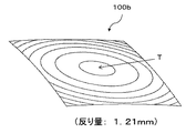
図2は、基板100bのシミュレーション結果における反り形状を図化したものである。図2は基板100bを斜め上から見た状態を示し、図中に表された複数のリングは等高線を示している。四角形状の基板の4つの頂点で形成される平面から中央のリングの中心部Tまでの距離が基板100bの反り量を示す。シミュレーション結果の反り量(図中の括弧内の数字)は実測値1.21mmと同じ値である。
FIG. 2 illustrates the warpage shape in the simulation result of the
<反りシミュレーションNo.2>
次に、図10に示す従来の基板100fについて反りシミュレーションの結果を説明する。従来の基板100fでは、5層の樹脂基材層(B1〜B5)に繊維束含有率が75%の基材を用いている。各配線層の残銅率は上述した例と同じ、すなわち図10に示した配線層C1から順に、32%、28%、37%、46%、52%、54%である。各配線層Cの厚み(10μm)、各樹脂基材層Bの厚み(30μm)および基板の大きさ(50mm×50mm)共に、上述した例と同じである。また、反りシミュレーションにおける基板の各部材の物性値についても、上述した例と同じである。
<Warpage simulation No. 2>
Next, the results of warping simulation for the
図11に、従来の基板100fのシミュレーション結果における反り形状を示す。シミュレーションの反り量は実測値1.51mmと同じ値である。前述した図2の結果と図11の結果を比較すると、図2(基板100b)では1.21mmの反り量を呈しているのに対し、図11(基板100f)では1.51mmの反り量を呈しており、本発明によって反りが約20%低減されていることがわかる。
FIG. 11 shows a warped shape in the simulation result of the
図10に示す、樹脂基材層Bの繊維束含有率が全層一律である基板100fでは、温度負荷時の反りは、各配線層Cにおける残銅率が各配線層間において異なることに起因する、熱膨張量の差によって生じる。基板100fの場合は、残銅率が配線層C1から順に、32%、28%、37%、46%、52%、54%と下側になるほど高くなるため、6層の配線層Cには、基板100fを上に凸に反らせる力が働く。
In the
これに対して、図2に示す基板100bでは、樹脂基材層B4の繊維束含有率(63%)が他の積層基材層の繊維束含有率(75%)と異なり、樹脂基材層B4のみが他の樹脂基材層より熱膨張量が大きいため、5層の樹脂基材層Bには基板を下に凸に反らせる力が働く。したがって、各配線層Cに働く上に凸に反らせる力に対して、各樹脂基材層Bに働く下に凸に反らせる力が打ち消す働きを持ち、反りが低減される。
On the other hand, in the
<反りシミュレーションNo.3>
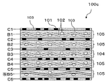
図3は基板100cの構成を示す。基板100cは、上部から順にC1〜C6までの6層の配線層を有し、各配線層Cの間に、上部から順にB1、B2(ともに積層基材層105)、B3(コア基材層104)、B4、B5(ともに積層基材層105)の5層の樹脂基材層を有している。また各配線層Cの残銅率は配線層C1から順に、32%、28%、37%、46%、52%、54%である。これらの配置および構成は、前述した基板100bと同じである。
<Warpage simulation No. 3>
FIG. 3 shows the configuration of the
図3の基板100cは、樹脂基材層B1、B2、B3、B4に繊維束含有率が75%の基材を用い、下側に位置する最外層の樹脂基材層B5(図3に※印を付与)のみに繊維束含有率が63%の基材を用いている。
The
上記以外の構成、すなわち各配線層Cの厚み、各樹脂基材層Bの厚みおよび基板の大きさは、基板100bと同じである。また、反りシミュレーションにおける基板の各部材の物性値についても、上述した例と同じである。
The configurations other than the above, that is, the thickness of each wiring layer C, the thickness of each resin base layer B, and the size of the substrate are the same as those of the
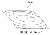
図4に、リフロー時の最高温度260℃を負荷した場合の反りシミュレーションの結果を示す。図4の結果を図11の結果と比較すると、図4(基板100c)では0.84mmの反り量を呈しているのに対し、図11(基板100f)では1.51mmの反り量を呈しており、本発明によって反りが約44%低減されていることがわかる。
FIG. 4 shows the results of warping simulation when the maximum temperature of 260 ° C. during reflow is loaded. Comparing the result of FIG. 4 with the result of FIG. 11, the warpage amount of 0.84 mm is exhibited in FIG. 4 (
図3に示す基板100cでは、樹脂基材層B5の繊維束含有率(63%)が他の積層基材層の繊維束含有率(75%)と異なり、樹脂基材層B5のみが他の樹脂基材層より熱膨張量が大きいため、5層の樹脂基材層Bには基板100cを下に凸に反らせる力が働く。したがって、各配線層Cに働く上に凸に反らせる力に対して、各樹脂基材層Bに働く下に凸に反らせる力が打ち消す働きを持ち、反りが低減される。
In the
基板100cおよび100bは、共にコア基材層104の下側の樹脂基材層(B4、B5)に、繊維束含有率が異なる樹脂基材層を配置しているが、基板100cは基板100bに比較して、基板の反りを低減する効果が大きい。これは、樹脂基材層の配置に起因するものであり、最外層に繊維束含有率が異なる樹脂基材層を配置した場合に、最も大きな効果が得られる。
In both the
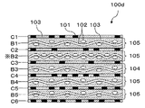
<反りシミュレーションNo.4>
図5に基板100dの構成を示す。基板100dは、上部から順にC1〜C6までの6層の配線層を有し、各配線層の間に、上部から順にB1、B2(ともに積層基材層105)、B3(コア基材層104)、B4、B5(ともに積層基材層105)の5層の樹脂基材層を有している。また各配線層の残銅率は、C1から順に、32%、28%、37%、46%、52%、54%である。これらの配置および構成は、前述した基板100bと同じである。
<Warpage simulation No. 4>
FIG. 5 shows the configuration of the
図5の基板100dは、樹脂基材層B1、B3、B4、B5に繊維束含有率が75%の基材を用い、コア基材層104を境にして上側に位置する樹脂基材層B2(図5に※印を付与)のみに繊維束含有率が81%の基材を用いている。
The
上記以外の構成、すなわち各配線層Cの厚み、各樹脂基材層Bの厚みおよび基板の大きさは、基板100bと同じである。また、反りシミュレーションにおける基板の各部材の物性値についても、上述した例と同じである。
The configurations other than the above, that is, the thickness of each wiring layer C, the thickness of each resin base layer B, and the size of the substrate are the same as those of the
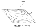
図6に、リフロー時の最高温度260℃を負荷した場合の反りシミュレーションの結果を示す。図6の結果を図11の結果と比較すると、図6(基板100d)では1.30mmの反り量を呈しているのに対し、図11(基板100f)では1.51mmの反り量を呈しており、本発明により反りが約13%低減されていることがわかる。
FIG. 6 shows the results of warping simulation when the maximum temperature of 260 ° C. during reflow is loaded. When the result of FIG. 6 is compared with the result of FIG. 11, the warpage amount of 1.30 mm is exhibited in FIG. 6 (
図6に示す基板100dでは、樹脂基材層B2の繊維束含有率(81%)が他の樹脂基材層の繊維束含有率(75%)と異なり、樹脂基材層B2のみが他の樹脂基材層より熱膨張量が小さいため、5層の樹脂基材層Bには基板を下に凸に反らせる力が働く。したがって、各配線層Cに働く上に凸に反らせる力に対して、各樹脂基材層Bに働く下に凸に反らせる力が打ち消す働きを持ち、反りが低減される。
In the
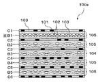
<反りシミュレーションNo.5>
図7に基板100eの構成を示す。基板100eは、上部から順にC1〜C6までの6層の配線層を有し、各配線層の間に、上部から順にB1、B2(ともに積層基材層105)、B3(コア基材層104)、B4、B5(ともに積層基材層105)の5層の樹脂基材層を有している。各配線層Cの残銅率は配線層C1から順に、32%、28%、37%、46%、52%、54%である。これらの配置および構成は、前述した基板100bと同じである。
<Warpage simulation No. 5>
FIG. 7 shows the configuration of the
図7の基板100eは、樹脂基材層B2、B3、B4、B5に繊維束含有率が75%の基材を用い、上側に位置する最外層の樹脂基材層B1(図7に※印を付与)のみに繊維束含有率が81%の基材を用いている。
The
上記以外の構成、すなわち各配線層Cの厚み、各樹脂基材層Bの厚みおよび基板の大きさは、基板100bと同じである。また、反りシミュレーションにおける基板の各部材の物性値についても、上述した例と同じである。
The configurations other than the above, that is, the thickness of each wiring layer C, the thickness of each resin base layer B, and the size of the substrate are the same as those of the
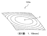
図8に、リフロー時の最高温度260℃を負荷した場合の反りシミュレーションの結果を示す。図8の結果を図11の結果と比較すると、図8(基板100e)では1.19mmの反り量を呈しているのに対し、図11(基板100f)では1.51mmの反り量を呈しており、本発明により約21%反りが低減されていることがわかる。
FIG. 8 shows the results of warping simulation when the maximum temperature of 260 ° C. during reflow is loaded. When the result of FIG. 8 is compared with the result of FIG. 11, the warpage amount of 1.19 mm is exhibited in FIG. 8 (
図7に示す基板100eでは、樹脂基材層B1の繊維束含有率(81%)が他の樹脂基材層の繊維束含有率(75%)と異なり、樹脂基材層B1のみが他の樹脂基材層より熱膨張量が小さいため、5層の樹脂基材層Bには基板を下に凸に反らせる力が働く。したがって、各配線層Cに働く上に凸に反らせる力に対して、各樹脂基材層Bに働く下に凸に反らせる力が打ち消す働きを持ち、反りが低減される。
In the
基板100eは基板100dに比較し、基板の反りを低減する効果が大きい。これは、シミュレーションNo.3で説明したのと同様に樹脂基材層の配置に起因するものであり、最外層に繊維束含有率が異なる樹脂基材層を配置した場合に、最も大きな効果が得られる。
The
表1は、上述した反りシミュレーションNo.1〜No.5の結果の一覧表である。表の各行には、シミュレーションNo.毎に、基板の各配線層(C1〜C6)の残銅率(%)、樹脂基材層(B1〜B5)の繊維束含有率(%)、および反りの程度が表示されている。 Table 1 shows the warpage simulation No. described above. 1-No. 5 is a list of 5 results. Each row of the table shows a simulation number. For each, the remaining copper ratio (%) of each wiring layer (C1 to C6) of the substrate, the fiber bundle content (%) of the resin base layer (B1 to B5), and the degree of warping are displayed.

前述したように基板の反りを低減させる方法として、樹脂基材層のうちの1層に、他の樹脂基材層の繊維束含有率より繊維束含有率が小さい樹脂基材層を用いる方法(シミュレーションNo.1、3)と、樹脂基材層のうちの1層に、他の積層基材層の繊維束含有率より繊維束含有率が大きい樹脂基材層を用いる方法(シミュレーションNo.4、5)がある。反りシミュレーションの結果から明らかなように、これらのいずれの方法においても、基板の各配線層Cに働く上に凸に反らせる力に対して、各樹脂基材層Bに下に凸に反らせる力を持たせ、基板の反りを低減できる。 As described above, as a method of reducing the warpage of the substrate, a method using a resin base layer having a fiber bundle content smaller than the fiber bundle content of another resin base layer (one of the resin base layers) ( Simulation No. 1, 3) and a method of using a resin base layer having a fiber bundle content larger than that of the other laminated base layer for one of the resin base layers (simulation No. 4) 5). As is apparent from the results of the warp simulation, in any of these methods, the force that acts on each wiring layer C of the substrate to bend upward and the force that causes the resin base layer B to warp downward is provided. The warpage of the substrate can be reduced.
なお、本実施の形態では、5層の樹脂基材層を持つ基板について説明したが、本発明は
これに限定されるものではない。また本実施の形態では、基板の中央にコア基材層104がある場合、すなわち配線層が偶数ある場合について説明したが、本発明はこれに限定されない。本発明は、基板の中央にコア基材層104がなく、基板が積層基材層105だけで構成されている場合、すなわち配線層が奇数ある場合についても、上述した実施の形態と同様の効果を発揮できる。
In the present embodiment, a substrate having five resin base layers has been described, but the present invention is not limited to this. In the present embodiment, the case where the core
例えば、基板の中央にある配線層を除いて、基板の下側にある配線層の残銅率の平均値が、上側にある配線層の残銅率の平均値よりも大きい場合、以下のいずれかの方法により、基板の反りを低減できる。
(1)基板の下側の積層基材層105のうち少なくとも1層に、他の積層基材層105の繊維束含有率より繊維束含有率が小さい樹脂基材層を用いる。
(2)基板の上側の積層基材層105のうち少なくとも1層に、他の積層基材層105の繊維束含有率より繊維束含有率が大きい樹脂基材層を用いる。
For example, when the average value of the remaining copper ratio of the wiring layer on the lower side of the substrate is larger than the average value of the remaining copper ratio of the upper wiring layer, except for the wiring layer in the center of the substrate, any of the following By this method, the warpage of the substrate can be reduced.
(1) A resin base material layer having a fiber bundle content smaller than the fiber bundle content of the other laminated
(2) A resin base material layer having a fiber bundle content larger than the fiber bundle content of the other laminated
また本実施の形態では、1層の樹脂基材層の繊維束含有率を、その層を除く他の樹脂基材層の繊維束含有率と異ならせる場合について説明したが、これに限定されない。本発明は、2層以上の樹脂基材層の繊維束含有率を、それらの層を除く他の樹脂基材層の繊維束含有率と異ならせる場合にも適用できる。 Moreover, although this Embodiment demonstrated the case where the fiber bundle content rate of one resin base material layer was made different from the fiber bundle content rate of the other resin base material layers except the layer, it is not limited to this. The present invention can also be applied to the case where the fiber bundle content of two or more resin base layers is different from the fiber bundle content of other resin base layers excluding those layers.
本発明の多層配線基板は、携帯電子機器をはじめ、デジタルモバイル商品などの電子回路形成のために搭載される配線基板として、多くの用途に適用できる。 The multilayer wiring board of the present invention can be applied to many uses as a wiring board mounted for forming electronic circuits for portable electronic devices and digital mobile products.
B1〜B5 樹脂基材層
C1〜C6 配線層
100b〜100e 多層配線基板
101 銅配線
102 繊維束
103 樹脂
104 コア基材層
105 積層基材層
108 ダミーパターン
B1 to B5 Resin base layer C1 to
Claims (6)
前記配線層間の熱膨張量の差を打ち消すように、
前記(n−1)層の樹脂基材層は、そのうちの1つの層と、それ以外の他の層との2種類の層があり、
前記1つの層と、前記他の層とは、層厚、並びに、前記繊維束の種類および太さは互いに同じであるが、前記1つの層だけが前記繊維束の間隔が前記他の層の前記繊維束の間隔と異なり、これにより、前記1つの層の繊維束含有率だけが、前記他の層の繊維束含有率と異なり、前記他の層の繊維含有率は互いに差異がない、多層配線基板。 Wiring made of conductive material and n (n is an integer of 4 or more) wiring layer composed of insulating resin, and (n-1) layer resin base material in which fiber bundle is impregnated with insulating resin A multilayer wiring board in which layers are laminated in an alternately overlapping state,
To negate the difference in thermal expansion between the wiring layers,
The (n-1) layer resin substrate layer includes a layer of one of its, there are two types of layers and the other other layer,
The one layer and the other layer have the same layer thickness and the same type and thickness of the fiber bundle, but only the one layer has the fiber bundle interval of the other layer. Unlike the spacing of the fiber bundles, thereby, the only fiber bundle content of one layer, the different from the fiber bundle content of the other layers, the fiber content of the other layers differences have greens each other, the multi-layer Wiring board.
かつn/2番目の前記樹脂基材層を境として、一方の実装面から数えて1番目から(n/2)番目までの前記配線層の残銅率の平均値が、(n/2+1)番目からn番目までの前記配線層の残銅率の平均値よりも大きく、
1番目から(n/2−1)番目までの前記樹脂基材層のうちの1層が前記1つの層であり、その繊維束含有率が、前記他の層の繊維束含有率よりも小さいことを特徴とする請求項1に記載の多層配線基板。 n is an even number,
And the average value of the remaining copper ratio of the wiring layer from the first to the (n / 2) -th counting from one mounting surface with the n / 2-th resin base material layer as a boundary is (n / 2 + 1) It is larger than the average value of the remaining copper ratio of the wiring layers from the nth to the nth,
From the first is one layer wherein one layer of said resin base layer up (n / 2-1) th, the fiber bundle content of its is, than the fiber bundle content of the other layers The multilayer wiring board according to claim 1, wherein the multilayer wiring board is small.
かつ(n+1)/2番目の前記配線層を境として、一方の実装面から数えて1番目から(n−1)/2番目までの前記配線層の残銅率の平均値が、(n+3)/2番目からn番目までの前記配線層の残銅率の平均値より大きく、
1番目から(n−1)/2番目までの前記樹脂基材層のうちの1層が前記1つの層であり、その繊維束含有率が、前記他の層の繊維束含有率よりも小さいことを特徴とする請求項1に記載の多層配線基板。 n is an odd number,
And, with the (n + 1) / 2th wiring layer as a boundary, the average value of the remaining copper ratio of the wiring layer from the first to (n-1) / 2th from the one mounting surface is (n + 3) / Larger than the average value of the remaining copper ratio of the wiring layer from the 2nd to the nth,
Is one layer wherein one layer of said resin base layer from the first to (n-1) / 2 th, fiber bundle content of its is, than the fiber bundle content of the other layers The multilayer wiring board according to claim 1, wherein the multilayer wiring board is small.
かつn/2番目の前記樹脂基材層を境として、一方の実装面から数えて1番目から(n/2)番目までの前記配線層の残銅率の平均値が、(n/2+1)番目からn番目までの前記配線層の残銅率の平均値よりも小さく、
1番目から(n/2−1)番目までの前記樹脂基材層のうちの1層が前記1つの層であり、その繊維束含有率が、前記他の層の繊維束含有率よりも大きいことを特徴とする請求項1に記載の多層配線基板。 n is an even number,
And the average value of the remaining copper ratio of the wiring layer from the first to the (n / 2) -th counting from one mounting surface with the n / 2-th resin base material layer as a boundary is (n / 2 + 1) Smaller than the average value of the remaining copper ratio of the wiring layers from the nth to the nth,
From the first is one layer wherein one layer of said resin base layer up (n / 2-1) th, the fiber bundle content of its is, than the fiber bundle content of the other layers The multilayer wiring board according to claim 1, wherein the multilayer wiring board is large.
かつ(n+1)/2番目の前記配線層を境として、一方の実装面から数えて1番目から(n−1)/2番目までの前記配線層の残銅率の平均値が、(n+3)/2番目からn番目までの前記配線層の残銅率の平均値より小さく、
1番目から(n−1)/2番目までの前記樹脂基材層のうちの1層が前記1つの層であり、その繊維束含有率が、前記他の層の繊維束含有率よりも大きいことを特徴とする請求項1に記載の多層配線基板。 n is an odd number,
And, with the (n + 1) / 2th wiring layer as a boundary, the average value of the remaining copper ratio of the wiring layer from the first to (n-1) / 2th from the one mounting surface is (n + 3) / Smaller than the average value of the remaining copper ratio of the wiring layer from the 2nd to the nth,
Is one layer wherein one layer of said resin base layer from the first to (n-1) / 2 th, fiber bundle content of its is, than the fiber bundle content of the other layers The multilayer wiring board according to claim 1, wherein the multilayer wiring board is large.
Priority Applications (3)
| Application Number | Priority Date | Filing Date | Title |
|---|---|---|---|
| JP2008108890A JP5225734B2 (en) | 2008-04-18 | 2008-04-18 | Multilayer wiring board |
| US12/193,311 US8022310B2 (en) | 2007-08-23 | 2008-08-18 | Multilayer wiring board |
| CN2008101459974A CN101374391B (en) | 2007-08-23 | 2008-08-22 | Multilayer wiring board |
Applications Claiming Priority (1)
| Application Number | Priority Date | Filing Date | Title |
|---|---|---|---|
| JP2008108890A JP5225734B2 (en) | 2008-04-18 | 2008-04-18 | Multilayer wiring board |
Publications (2)
| Publication Number | Publication Date |
|---|---|
| JP2009260123A JP2009260123A (en) | 2009-11-05 |
| JP5225734B2 true JP5225734B2 (en) | 2013-07-03 |
Family
ID=41387161
Family Applications (1)
| Application Number | Title | Priority Date | Filing Date |
|---|---|---|---|
| JP2008108890A Expired - Fee Related JP5225734B2 (en) | 2007-08-23 | 2008-04-18 | Multilayer wiring board |
Country Status (1)
| Country | Link |
|---|---|
| JP (1) | JP5225734B2 (en) |
Families Citing this family (5)
| Publication number | Priority date | Publication date | Assignee | Title |
|---|---|---|---|---|
| JP5471870B2 (en) * | 2010-06-17 | 2014-04-16 | 富士通株式会社 | Wiring board |
| JP2015038911A (en) | 2012-09-27 | 2015-02-26 | イビデン株式会社 | Printed wiring board and method of manufacturing printed wiring board |
| US9384314B2 (en) | 2014-02-28 | 2016-07-05 | International Business Machines Corporation | Reduction of warpage of multilayered substrate or package |
| JP6386252B2 (en) * | 2014-04-23 | 2018-09-05 | イビデン株式会社 | Printed wiring board |
| JP6878794B2 (en) * | 2016-08-31 | 2021-06-02 | 大日本印刷株式会社 | Perforated substrate manufacturing method and perforated substrate |
Family Cites Families (4)
| Publication number | Priority date | Publication date | Assignee | Title |
|---|---|---|---|---|
| JP2001111218A (en) * | 1999-10-13 | 2001-04-20 | Hitachi Ltd | Multilayer printed circuit board and electronic device |
| JP2001217514A (en) * | 2000-02-03 | 2001-08-10 | Denso Corp | Multi-layered wiring board |
| JP2003324282A (en) * | 2002-04-26 | 2003-11-14 | Matsushita Electric Works Ltd | Bonding sheet for laminated layer plate including internal layer circuit, laminated layer plate including internal layer circuit formed using the bonding sheet and method of manufacturing the bonding sheet |
| JP2004026997A (en) * | 2002-06-25 | 2004-01-29 | Noritake Co Ltd | Inorganic woven fabric-reinforced resin substrate, inorganic woven fabric, and method for opening inorganic woven fabric |
-
2008
- 2008-04-18 JP JP2008108890A patent/JP5225734B2/en not_active Expired - Fee Related
Also Published As
| Publication number | Publication date |
|---|---|
| JP2009260123A (en) | 2009-11-05 |
Similar Documents
| Publication | Publication Date | Title |
|---|---|---|
| JP5302635B2 (en) | Multilayer wiring board | |
| JP5497334B2 (en) | Multilayer wiring board | |
| US8686821B2 (en) | Inductor structure | |
| JP5225734B2 (en) | Multilayer wiring board | |
| US8022310B2 (en) | Multilayer wiring board | |
| JP2010135418A (en) | Wiring board and electronic component device | |
| KR20110034027A (en) | Wiring board and method for manufacturing same | |
| JP4869007B2 (en) | Printed wiring board | |
| JP2011023521A (en) | Flexible wiring board | |
| CN103857174B (en) | Printed circuit board and manufacturing methods | |
| JP2011171473A (en) | Printed wiring board | |
| JP5194951B2 (en) | Circuit board manufacturing method | |
| JP5506984B2 (en) | Multilayer wiring board | |
| US20150062850A1 (en) | Printed circuit board | |
| JP5001868B2 (en) | Multilayer board manufacturing method | |
| KR101951654B1 (en) | Manufacturing Method of Printed Circuit Board to Improve Flatness | |
| JP2018190765A (en) | Rigid-flex multilayer printed wiring substrate | |
| KR20140148111A (en) | Rigid flexible printed circuit board and method for manufacturing thereof | |
| JP2003188493A (en) | Method of manufacturing circuit board | |
| JP7101454B2 (en) | Optical / electric mixed circuit board | |
| JP2017159615A (en) | Metal-clad laminate | |
| JP5023796B2 (en) | Printed wiring board and manufacturing method thereof | |
| JP2009054773A (en) | Multilayer wiring board and manufacturing method thereof | |
| JP2024013103A (en) | Core substrate, manufacturing method thereof, and multilayer wiring substrate | |
| KR102194717B1 (en) | Printed circuit board and method of manufacturing the same |
Legal Events
| Date | Code | Title | Description |
|---|---|---|---|
| A621 | Written request for application examination |
Free format text: JAPANESE INTERMEDIATE CODE: A621 Effective date: 20101227 |
|
| A977 | Report on retrieval |
Free format text: JAPANESE INTERMEDIATE CODE: A971007 Effective date: 20120406 |
|
| A131 | Notification of reasons for refusal |
Free format text: JAPANESE INTERMEDIATE CODE: A131 Effective date: 20120412 |
|
| A521 | Request for written amendment filed |
Free format text: JAPANESE INTERMEDIATE CODE: A523 Effective date: 20120606 |
|
| A02 | Decision of refusal |
Free format text: JAPANESE INTERMEDIATE CODE: A02 Effective date: 20121108 |
|
| A521 | Request for written amendment filed |
Free format text: JAPANESE INTERMEDIATE CODE: A523 Effective date: 20130108 |
|
| A911 | Transfer to examiner for re-examination before appeal (zenchi) |
Free format text: JAPANESE INTERMEDIATE CODE: A911 Effective date: 20130116 |
|
| TRDD | Decision of grant or rejection written | ||
| A01 | Written decision to grant a patent or to grant a registration (utility model) |
Free format text: JAPANESE INTERMEDIATE CODE: A01 Effective date: 20130215 |
|
| A61 | First payment of annual fees (during grant procedure) |
Free format text: JAPANESE INTERMEDIATE CODE: A61 Effective date: 20130313 |
|
| R150 | Certificate of patent or registration of utility model |
Ref document number: 5225734 Country of ref document: JP Free format text: JAPANESE INTERMEDIATE CODE: R150 Free format text: JAPANESE INTERMEDIATE CODE: R150 |
|
| FPAY | Renewal fee payment (event date is renewal date of database) |
Free format text: PAYMENT UNTIL: 20160322 Year of fee payment: 3 |
|
| LAPS | Cancellation because of no payment of annual fees |