JP5218521B2 - Imprint method and transfer substrate and adhesive used therefor - Google Patents
Imprint method and transfer substrate and adhesive used therefor Download PDFInfo
- Publication number
- JP5218521B2 JP5218521B2 JP2010236181A JP2010236181A JP5218521B2 JP 5218521 B2 JP5218521 B2 JP 5218521B2 JP 2010236181 A JP2010236181 A JP 2010236181A JP 2010236181 A JP2010236181 A JP 2010236181A JP 5218521 B2 JP5218521 B2 JP 5218521B2
- Authority
- JP
- Japan
- Prior art keywords
- substrate
- adhesion layer
- transfer
- group
- workpiece
- Prior art date
- Legal status (The legal status is an assumption and is not a legal conclusion. Google has not performed a legal analysis and makes no representation as to the accuracy of the status listed.)
- Active
Links
Images


Classifications
-
- B—PERFORMING OPERATIONS; TRANSPORTING
- B29—WORKING OF PLASTICS; WORKING OF SUBSTANCES IN A PLASTIC STATE IN GENERAL
- B29C—SHAPING OR JOINING OF PLASTICS; SHAPING OF MATERIAL IN A PLASTIC STATE, NOT OTHERWISE PROVIDED FOR; AFTER-TREATMENT OF THE SHAPED PRODUCTS, e.g. REPAIRING
- B29C59/00—Surface shaping of articles, e.g. embossing; Apparatus therefor
- B29C59/02—Surface shaping of articles, e.g. embossing; Apparatus therefor by mechanical means, e.g. pressing
- B29C59/026—Surface shaping of articles, e.g. embossing; Apparatus therefor by mechanical means, e.g. pressing of layered or coated substantially flat surfaces
-
- B—PERFORMING OPERATIONS; TRANSPORTING
- B29—WORKING OF PLASTICS; WORKING OF SUBSTANCES IN A PLASTIC STATE IN GENERAL
- B29C—SHAPING OR JOINING OF PLASTICS; SHAPING OF MATERIAL IN A PLASTIC STATE, NOT OTHERWISE PROVIDED FOR; AFTER-TREATMENT OF THE SHAPED PRODUCTS, e.g. REPAIRING
- B29C59/00—Surface shaping of articles, e.g. embossing; Apparatus therefor
- B29C59/005—Surface shaping of articles, e.g. embossing; Apparatus therefor characterised by the choice of material
-
- B—PERFORMING OPERATIONS; TRANSPORTING
- B82—NANOTECHNOLOGY
- B82Y—SPECIFIC USES OR APPLICATIONS OF NANOSTRUCTURES; MEASUREMENT OR ANALYSIS OF NANOSTRUCTURES; MANUFACTURE OR TREATMENT OF NANOSTRUCTURES
- B82Y10/00—Nanotechnology for information processing, storage or transmission, e.g. quantum computing or single electron logic
-
- B—PERFORMING OPERATIONS; TRANSPORTING
- B82—NANOTECHNOLOGY
- B82Y—SPECIFIC USES OR APPLICATIONS OF NANOSTRUCTURES; MEASUREMENT OR ANALYSIS OF NANOSTRUCTURES; MANUFACTURE OR TREATMENT OF NANOSTRUCTURES
- B82Y40/00—Manufacture or treatment of nanostructures
-
- G—PHYSICS
- G03—PHOTOGRAPHY; CINEMATOGRAPHY; ANALOGOUS TECHNIQUES USING WAVES OTHER THAN OPTICAL WAVES; ELECTROGRAPHY; HOLOGRAPHY
- G03F—PHOTOMECHANICAL PRODUCTION OF TEXTURED OR PATTERNED SURFACES, e.g. FOR PRINTING, FOR PROCESSING OF SEMICONDUCTOR DEVICES; MATERIALS THEREFOR; ORIGINALS THEREFOR; APPARATUS SPECIALLY ADAPTED THEREFOR
- G03F7/00—Photomechanical, e.g. photolithographic, production of textured or patterned surfaces, e.g. printing surfaces; Materials therefor, e.g. comprising photoresists; Apparatus specially adapted therefor
- G03F7/0002—Lithographic processes using patterning methods other than those involving the exposure to radiation, e.g. by stamping
-
- H—ELECTRICITY
- H01—ELECTRIC ELEMENTS
- H01L—SEMICONDUCTOR DEVICES NOT COVERED BY CLASS H10
- H01L21/00—Processes or apparatus adapted for the manufacture or treatment of semiconductor or solid state devices or of parts thereof
- H01L21/02—Manufacture or treatment of semiconductor devices or of parts thereof
- H01L21/027—Making masks on semiconductor bodies for further photolithographic processing not provided for in group H01L21/18 or H01L21/34
- H01L21/0271—Making masks on semiconductor bodies for further photolithographic processing not provided for in group H01L21/18 or H01L21/34 comprising organic layers
- H01L21/0273—Making masks on semiconductor bodies for further photolithographic processing not provided for in group H01L21/18 or H01L21/34 comprising organic layers characterised by the treatment of photoresist layers
- H01L21/0274—Photolithographic processes
Description
本発明は、被加工物に所望のパターン(線、模様等の図形であり、平坦面も含む)を転写形成するインプリント方法と、このインプリント方法に使用する転写基材と密着剤に関する。 The present invention relates to an imprint method for transferring and forming a desired pattern (a figure such as a line or a pattern, including a flat surface) on a workpiece, and a transfer substrate and an adhesive used in the imprint method.
微細加工技術として、近年インプリント方法に注目が集まっている。インプリント方法は、基体の表面に微細な凹凸構造を形成したモールド(型部材)を用い、凹凸構造を被加工物に転写することで微細構造を等倍転写するパターン形成技術である。
このインプリント方法の一つとして、光インプリント法が知られている。この光インプリント法では、例えば、インプリント用の転写基材に被加工物として光硬化性の樹脂層を形成し、この樹脂層に所望の凹凸構造を有するモールド(型部材)を押し当てる。そして、この状態でモールド側から樹脂層に紫外線を照射して硬化させ、その後、モールドを樹脂層から引き離す。これにより、モールドが有する凹凸が反転した凹凸構造を被加工物である樹脂層に形成することができる。このような光インプリント法は、従来のフォトリソグラフィ技術では形成が困難なナノメートルオーダーの微細パターンの形成が可能であり、次世代リソグラフィ技術として有望視されている。
このようなインプリント方法では、硬化した樹脂層からモールドを引き離す際に、樹脂層がモールドに付着するのを防止する必要がある。この付着防止の方法として、モールド表面へ離型処理を施す方法(特許文献1)、インプリント用の転写基材と硬化した樹脂層との間に密着層を介在させて両者の密着性を向上させる方法(特許文献2、3)、あるいは、モールド表面に設けた光触媒性物質膜に紫外線を照射して、硬化した樹脂層との離型性を向上させる方法(特許文献4)等が提案されている。
In recent years, attention has been focused on the imprint method as a fine processing technique. The imprint method is a pattern forming technique in which a fine structure is transferred at an equal magnification by using a mold (mold member) in which a fine concavo-convex structure is formed on the surface of a substrate and transferring the concavo-convex structure to a workpiece.
As one of the imprint methods, an optical imprint method is known. In this optical imprinting method, for example, a photocurable resin layer is formed as a workpiece on a transfer substrate for imprinting, and a mold (mold member) having a desired uneven structure is pressed against the resin layer. In this state, the resin layer is irradiated with ultraviolet rays to be cured from the mold side, and then the mold is pulled away from the resin layer. Thereby, the uneven structure in which the unevenness of the mold is inverted can be formed on the resin layer as the workpiece. Such an optical imprint method is capable of forming a fine pattern on the order of nanometers, which is difficult to form with conventional photolithography technology, and is promising as a next-generation lithography technology.
In such an imprint method, it is necessary to prevent the resin layer from adhering to the mold when the mold is pulled away from the cured resin layer. As a method for preventing this adhesion, a method of releasing the mold surface (Patent Document 1), and an adhesion layer is interposed between the imprint transfer substrate and the cured resin layer to improve the adhesion between the two. Proposed (
上述のモールドへの樹脂層の付着防止方法のうち、インプリント用の転写基材と硬化した樹脂層との密着性を向上させる方法では、転写基材との間で結合を形成するような官能基、および、樹脂層との間で結合を形成するような官能基を有する材料を用いて密着層が形成されている。このような材料として、シランカップリング剤が挙げられている。そして、転写基材との反応点が多いほど密着性向上には有利であることから、転写基材との結合に供する官能基がケイ素原子に3個結合したシランカップリング剤が好適に使用されている。 Among the methods for preventing the adhesion of the resin layer to the mold described above, the method for improving the adhesion between the imprinting transfer substrate and the cured resin layer is a function that forms a bond with the transfer substrate. The adhesion layer is formed using a material having a functional group that forms a bond with the group and the resin layer. A silane coupling agent is mentioned as such a material. Since the more reaction points with the transfer substrate, the more advantageous the adhesion is. Therefore, a silane coupling agent in which three functional groups for bonding to the transfer substrate are bonded to silicon atoms is preferably used. ing.
しかし、このようなシランカップリング剤を用いた従来の付着防止方法では、硬化した樹脂層からモールドを引き離す際に、樹脂層の一部がモールドに付着して転写欠陥を生じることがあり、安定したパターン形成を行うことができないという問題があった。また、上記のシランカップリング剤は、大気中の水分と加水分解反応を生じて劣化し易いため、長期保管が難しく、製造工程管理が煩雑となったり、パターン形成におけるコスト低減に支障を来すという問題もあった。さらに、スピンコート法を用いてシランカップリング剤を転写基材に塗布して密着層を形成する場合、転写基材の端部や、転写基材表面の段差部分で密着層の厚みが大きくなり、高精度のパターン形成を行うことができないという問題があった。
本発明は、上述のような実情に鑑みてなされたものであり、モールドと樹脂層との離型時の転写欠陥の発生を防止したインプリント方法と、このようなインプリント方法を可能とする転写基材、密着剤を提供することを目的とする。
However, in the conventional adhesion prevention method using such a silane coupling agent, when the mold is pulled away from the cured resin layer, a part of the resin layer may adhere to the mold and cause a transfer defect. There is a problem that the formed pattern cannot be formed. In addition, the above silane coupling agent is prone to degradation due to hydrolysis reaction with moisture in the atmosphere, so long-term storage is difficult, manufacturing process management becomes complicated, and cost reduction in pattern formation is hindered. There was also a problem. Furthermore, when a silane coupling agent is applied to a transfer substrate using a spin coating method to form an adhesion layer, the thickness of the adhesion layer increases at the edge of the transfer substrate or at a step on the surface of the transfer substrate. There is a problem that high-precision pattern formation cannot be performed.
The present invention has been made in view of the above circumstances, and enables an imprint method that prevents the occurrence of a transfer defect at the time of releasing a mold and a resin layer, and enables such an imprint method. An object is to provide a transfer substrate and an adhesive.
本発明者は、シランカップリング剤と転写基材との結合反応よりも、シランカップリング剤の分子間の縮合反応による鎖状や網目状の層が生じやすく、転写基材との結合に供する官能基がケイ素原子に3個結合したシランカップリング剤を用いて形成した密着層では、表面に凸部が生じて平坦性が低下することに着目して本発明をなすに至った。
すなわち、上記のような目的を達成するために、本発明のインプリント方法は、所望の形状の転写形状部を有するモールドと転写基材との間に被加工物を介在させ、該被加工物に前記転写形状部の形状を転写するインプリント方法において、基材に密着層を形成して転写基材を作製する密着層形成工程と、前記モールドと前記密着層との間に前記被加工物が介在するようして前記モールドと前記転写基材とを近接させ前記被加工物を前記転写形状部に充填する充填工程と、前記被加工物を硬化させる硬化工程と、前記被加工物から前記モールドを引き離す離型工程と、を有し、前記密着層形成工程は、1個の加水分解性基と2個の不活性基とを有する4価の原子と該原子に結合した反応性官能基とを1分子中に有する化合物を含有する密着剤を、前記基材に接触させ、その後、洗浄する工程を有し、高さ5nm以上の凸部が存在しない密着層を形成するものであるような構成とした。
The present inventor is more likely to form a chain or network layer due to a condensation reaction between molecules of the silane coupling agent than the binding reaction between the silane coupling agent and the transfer substrate, and is used for bonding with the transfer substrate. In the adhesion layer formed using a silane coupling agent in which three functional groups are bonded to silicon atoms, the present invention has been made by paying attention to the fact that convex portions are formed on the surface and flatness is lowered.
That is, in order to achieve the above object, the imprinting method of the present invention interposes a workpiece between a mold having a transfer shape portion having a desired shape and a transfer substrate, and the workpiece In the imprint method for transferring the shape of the transfer shape portion to the substrate, an adhesion layer forming step of forming an adhesion layer on a substrate to produce a transfer substrate, and the workpiece between the mold and the adhesion layer The mold and the transfer base material are brought close to each other so as to intervene, the filling step for filling the transfer shape portion with the workpiece, the curing step for curing the workpiece, and the workpiece from the workpiece A release step for separating the mold, and the adhesion layer forming step includes a tetravalent atom having one hydrolyzable group and two inactive groups, and a reactive functional group bonded to the atom. Adhesive containing a compound having 1 in a molecule Is brought into contact with the substrate, then, have a step of washing was that such as to form an adhesive layer projecting portion of the above height of 5nm is not present configuration.
本発明の他の態様として、前記密着層形成工程における洗浄は、極性溶媒を使用するような構成とした。
本発明の他の態様として、前記密着剤の前記4価の原子はケイ素であるような構成とした。
本発明の他の態様として、前記基材として周囲に対して凸構造となった凸状平坦面を有する基材を使用し、前記密着層形成工程では、該凸状平坦面に密着層を形成して転写基材を作製するような構成とした。
本発明の他の態様として、前記密着層形成工程において、前記密着剤をスピンコート法により前記基材に塗布するような構成とした。
本発明の転写基材は、基材と、該基材上に位置する密着層とを備えるインプリント用の転写基材であって、密着層は、酸素原子を介して前記基材に結合するとともに2個の不活性基とを有する4価の原子と、該原子に結合した反応性官能基と、を有し、高さ5nm以上の凸部が存在しないような構成とした。
本発明の他の態様として、隣接する前記4価の原子同士は結合していないような構成とした。
本発明の他の態様として、前記4価の原子はケイ素であるような構成とした。
本発明の他の態様として、前記基材は、周囲に対して凸構造となった凸状平坦面を有し、該凸状平坦面に前記密着層を備えるような構成とした。
As another aspect of the present invention, the cleaning in the adhesion layer forming step is configured to use a polar solvent.
As another aspect of the present invention, the tetravalent atom of the adhesive is configured to be silicon.
As another aspect of the present invention, a base material having a convex flat surface with a convex structure with respect to the surrounding is used as the base material, and in the adhesion layer forming step, an adhesion layer is formed on the convex flat surface. Thus, the transfer base material was produced.
As another aspect of the present invention, in the adhesion layer forming step, the adhesion agent is applied to the substrate by a spin coating method.
The transfer base material of the present invention is a transfer base material for imprint including a base material and an adhesion layer located on the base material, and the adhesion layer is bonded to the base material through oxygen atoms. and tetravalent atom having a two inert radicals together, possess a reactive functional group attached to the atom, and was like protrusions above the height 5nm absence configuration.
As another aspect of the present invention, the adjacent tetravalent atoms are not bonded to each other.
In another embodiment of the present invention, the tetravalent atom is silicon.
As another aspect of the present invention, the base material has a convex flat surface having a convex structure with respect to the periphery, and the adhesive flat layer is provided with the adhesion layer.
本発明のインプリント方法は、密着層形成工程において使用する密着剤を構成する4価の原子が加水分解性基を1個のみ有しているので、この加水分解性基が加水分解を受けた後、基材表面の水酸基が存在する反応点との結合(水素結合を経て、酸素原子を介した共有結合を形成)がなされるとともに、4価の原子が2個の不活性基を有しているので、基材表面と結合した4価の原子は、他の分子の4価の原子と結合を生じることが抑制され、さらに、基材と未反応の密着剤が洗浄によって除去されるので、基材の端部や、基材表面の段差部分においても不要な密着剤が存在せず、均一な厚みの密着層を備えた転写基材の形成が可能であり、その後の充填工程、硬化工程において、密着層の反応性官能基と被加工物とが反応して結合を生じ、硬化した被加工物が密着層を介して転写基材に確実に密着した状態となり、これにより、離型工程では、モールドへの被加工物の付着による転写欠陥を防止することができる。 In the imprint method of the present invention, since the tetravalent atom constituting the adhesive used in the adhesion layer forming step has only one hydrolyzable group, this hydrolyzable group was hydrolyzed. After that, a bond with a reaction point where a hydroxyl group exists on the substrate surface (through a hydrogen bond, a covalent bond via an oxygen atom is formed) and a tetravalent atom has two inactive groups. Therefore, the tetravalent atom bonded to the substrate surface is suppressed from forming a bond with the tetravalent atom of other molecules, and further, the substrate and the unreacted adhesive are removed by washing. In addition, there is no unnecessary adhesion agent at the edge of the substrate or at the stepped portion of the substrate surface, and it is possible to form a transfer substrate having an adhesion layer with a uniform thickness. In the process, the reactive functional group of the adhesion layer reacts with the workpiece to form a bond, The workpiece is a state of being securely adhered to the transfer substrate via the adhesion layer ized, thereby, in the releasing process, it is possible to prevent transfer defects caused by adhesion of the workpiece to the mold.
本発明の転写基材は、酸素原子を介して前記基材に結合するとともに2個の不活性基とを有する4価の原子と、該原子に結合した反応性官能基と、を有する密着層を備えており、このような密着層の表面は平坦性に優れており、インプリントにおいて密着層上に配設された被加工物を、密着層の表面に位置している反応性官能基との反応によって確実に結合保持し、モールドとの離型時にモールドに付着して剥離させることを防止することができる。 The transfer substrate of the present invention has an adhesive layer having a tetravalent atom bonded to the substrate via an oxygen atom and having two inactive groups, and a reactive functional group bonded to the atom. The surface of such an adhesion layer is excellent in flatness, and the work piece disposed on the adhesion layer in imprinting has a reactive functional group located on the surface of the adhesion layer. Thus, it is possible to securely bond and hold by the above reaction, and to prevent it from adhering to the mold and peeling off from the mold.
本発明の密着剤は、1個の加水分解性基と2個の不活性基とを有する4価の原子と該原子に結合した反応性官能基とを1分子中に有する化合物を含むので、加水分解性基が加水分解を受けることにより、基材表面の水酸基との水素結合を介して4価の原子が基材表面に移行し、さらに、脱水縮合反応を経て基材表面と強固な共有結合を生成し、このように基材表面に結合した4価の原子は、2個の不活性基とを有しているので他の分子の4価の原子との間で縮合反応による結合を生じることが抑制され、密着剤の凝集物生成が防止され、また、基材と未反応の密着剤は、例えば、二量体を形成することはあっても、基材表面に結合した4価の原子とは結合していないため洗浄で除去することができ、これにより、均一な厚みの密着層の形成が可能である。また、ケイ素が複数の加水分解性基を有するシランカップリング剤に比べて、保存安定性に優れている。 Since the adhesive of the present invention contains a compound having a tetravalent atom having one hydrolyzable group and two inactive groups and a reactive functional group bonded to the atom in one molecule, When the hydrolyzable group is hydrolyzed, the tetravalent atoms are transferred to the substrate surface through hydrogen bonds with the hydroxyl group on the substrate surface, and are further firmly shared with the substrate surface through a dehydration condensation reaction. A tetravalent atom that forms a bond and thus binds to the surface of the substrate has two inactive groups. Therefore, a bond due to a condensation reaction is formed between the tetravalent atom of another molecule. Occurrence is suppressed, aggregate formation of the adhesive agent is prevented, and the base material and the unreacted adhesive agent form, for example, a dimer, but a tetravalent bonded to the base material surface. It can be removed by washing because it is not bonded to any other atoms, and this makes it possible to form an adhesion layer with a uniform thickness. It is a function. Moreover, compared with the silane coupling agent in which silicon has a some hydrolyzable group, it is excellent in storage stability.
以下、本発明の実施形態について図面を参照しながら説明する。
[インプリント用の転写基材]
図1は、本発明の転写基材の一実施形態を示す部分断面図である。図1において、転写基材1は、基材2と、基材2の一方の面2aに位置する密着層3とを備えている。
転写基材1を構成する基材2は、例えば、石英やソーダライムガラス、ホウ珪酸ガラス等のガラス、シリコンや酸化シリコン、窒化シリコン、ガリウム砒素、窒化ガリウム等の半導体、クロム、タンタル、アルミニウム、ニッケル、チタン、銅、鉄、コバルト等の金属基板、あるいは、これらの材料の任意の組み合わせからなる複合材料基板であってよい。また、基材2は所望のパターン構造物が面2a側に形成されたものであってもよい。このパターン構造物としては、特に限定されず、半導体やディスプレイ等に用いられる微細配線や、フォトニック結晶構造、光導波路、ホログラフィのような光学的構造等が挙げられる。
Hereinafter, embodiments of the present invention will be described with reference to the drawings.
[Transfer substrate for imprint]
FIG. 1 is a partial cross-sectional view showing an embodiment of a transfer substrate of the present invention. In FIG. 1, a transfer substrate 1 includes a
The
また、転写基材1を構成する密着層3は、酸素原子を介して基材2に結合するとともに2個の不活性基とを有する4価の原子と、この原子に結合した反応性官能基と、を有するものである。図2は、このような密着層3の分子構造を説明するための図である。図2に示されるように、4価の原子Mは、酸素原子Oを介して基材2に結合するとともに2個の不活性基X、X′を有している。また、4価の原子Mには反応性官能基Yが結合している。そして、隣接する4価の原子M同士は結合しておらず、したがって密着層3を構成する分子間の縮合反応により形成された鎖状や網目状の層が存在せず、単分子構造となっていると考えられる。
密着層3を構成する4価の原子Mは、ケイ素、チタン等とすることができ、この中でケイ素が好適に用いられる。また、不活性基X、X′は加水分解反応を生じない基であり、例えば、メチル基、エチル基、n−プロピル基、イソプロピル基、n−ブチル基、イソブチル基、sec−ブチル基、tert−ブチル基、ベンジル基等のアルキル基であり、これらは同一であっても異なってもよい。また、反応性官能基Yは、被加工物である有機成分との反応を生じる基であり、例えば、アミノ基、エポキシ基、メルカプト基、スルフィド基、アシル基、イソシアネート基、不飽和炭化水素基からなる群から選択される基であり、結合手−(CH2)n−を介して4価の原子Mに結合している。不飽和炭化水素基としては、ビニル基、メタクリル基、アクリロキシ基、メタクリロキシ基等を挙げることができる。また、結合手のnは1〜10の整数であるが、密着層を構成する分子の密度分布をより均一にするためには分子量が低いことが好ましいので、nは1〜3の範囲が好適である。
In addition, the
The tetravalent atom M constituting the
このような本発明の転写基材1は、密着層3を構成する分子間の縮合反応により形成される鎖状や網目状の層のような不均一な層が存在せず、表面の平坦性に優れる。また、密着層3は、鎖状や網目状の層構造をとらず異物が付着しにくい構造を有しているため、離型時における被加工物の欠陥原因となりうる密着層の不均一性あるいは異物による微細な凸部の発生を低減でき、転写欠陥を防止することができる。また、基材2の表面と結合した4価の原子は、他の分子の4価の原子と結合を生じることが抑制され、より高密度に基材表面と密着し、インプリントにおいて密着層3上に配設された被加工物を、密着層3の表面に位置している反応性官能基Yとの反応によって確実に結合保持することができる。
尚、上述のインプリント用の転写基材の実施形態は例示であり、本発明はこれに限定されるものではない。
Such a transfer substrate 1 of the present invention does not have a non-uniform layer such as a chain-like or network-like layer formed by a condensation reaction between molecules constituting the
The embodiment of the transfer substrate for imprint described above is an exemplification, and the present invention is not limited to this.
[密着剤]
上記のような転写基材1の密着層3を形成するには、1個の加水分解性基と2個の不活性基とを有する4価の原子と、この原子に結合した反応性官能基と、を1分子中に有する化合物を含む本発明の密着剤を使用することができる。以下に本発明の密着剤について説明する。
本発明の密着剤は、上記のように、1個の加水分解性基と2個の不活性基とを有する4価の原子と該原子に結合した反応性官能基とを1分子中に有する化合物を含むものである。このような化合物の一例として、4価の原子がケイ素である下記式(1)で表される化合物を挙げることができる。

In order to form the
As described above, the adhesive of the present invention has a tetravalent atom having one hydrolyzable group and two inactive groups and a reactive functional group bonded to the atom in one molecule. Contains compounds. An example of such a compound is a compound represented by the following formula (1) in which a tetravalent atom is silicon.
上記のアルコキシ基Rとしては、例えば、メトキシ基、エトキシ基、プロポキシ基、ブトキシ基、イソプロポキシ基、シクロヘキシルオキシ基等を挙げることができる。また、上記のアルキル基X1、X2としては、メチル基、エチル基、n−プロピル基、イソプロピル基、n−ブチル基、イソブチル基、sec−ブチル基、tert−ブチル基、ベンジル基等を挙げることができる。さらに、上記の不飽和炭化水素基としては、ビニル基、メタクリル基、アクリロキシ基、メタクリロキシ基等を挙げることができる。
反応性官能基Yは、被加工物である有機成分を考慮して適宜選択することができ、例えば、被加工物が酸、エステル、エポキシ、ケトン、ハロゲン化物を含有する有機成分であれば、反応性官能基Yとしてアミノ基を選択することができ、被加工物がアミノ基やカルボキシル基を含有する有機成分であれば、反応性官能基Yとしてエポキシ基を選択することができ、被加工物がチオールを含有する有機成分であれば、反応性官能基Yとしてメルカプト基を選択することができ、被加工物がアクリルモノマーを含有する有機成分であれば、反応性官能基Yとして不飽和炭化水素基を選択することができる。
Examples of the alkoxy group R include a methoxy group, an ethoxy group, a propoxy group, a butoxy group, an isopropoxy group, and a cyclohexyloxy group. The alkyl groups X 1 and X 2 include methyl group, ethyl group, n-propyl group, isopropyl group, n-butyl group, isobutyl group, sec-butyl group, tert-butyl group, benzyl group and the like. Can be mentioned. Furthermore, examples of the unsaturated hydrocarbon group include a vinyl group, a methacryl group, an acryloxy group, and a methacryloxy group.
The reactive functional group Y can be appropriately selected in consideration of the organic component that is the workpiece. For example, if the workpiece is an organic component containing an acid, ester, epoxy, ketone, or halide, An amino group can be selected as the reactive functional group Y, and if the workpiece is an organic component containing an amino group or a carboxyl group, an epoxy group can be selected as the reactive functional group Y. If the product is an organic component containing a thiol, a mercapto group can be selected as the reactive functional group Y, and if the workpiece is an organic component containing an acrylic monomer, the reactive functional group Y is unsaturated. A hydrocarbon group can be selected.
上記式(1)で表される化合物の具体例としては、(3−アクリロキシメチル)ジメチルメトキシシラン、(3−アクリロキシエチル)ジメチルメトキシシラン、(3−アクリロキシプロピル)ジメチルメトキシシラン、(3−メタクリロキシメチル)ジメチルメトキシシラン、(3−メタクリロキシエチル)ジメチルメトキシシラン、(3−メタクリロキシプロピル)ジメチルメトキシシラン等を挙げることができる。また、形成した密着層の分子の密度分布をより均一にするためには、立体障害の低減等を考慮して、上記式(1)で表される化合物の分子量が低いことが好ましく、アルコキシ基Rとしてメトキシ基またはエトキシ基を有し、アルキル基X1、X2としては、メチル基、エチル基、あるいは、プロピル基を有し、nが1〜3である化合物が好ましい。 Specific examples of the compound represented by the above formula (1) include (3-acryloxymethyl) dimethylmethoxysilane, (3-acryloxyethyl) dimethylmethoxysilane, (3-acryloxypropyl) dimethylmethoxysilane, ( Examples include 3-methacryloxymethyl) dimethylmethoxysilane, (3-methacryloxyethyl) dimethylmethoxysilane, and (3-methacryloxypropyl) dimethylmethoxysilane. In order to make the density distribution of the molecules in the formed adhesion layer more uniform, the molecular weight of the compound represented by the above formula (1) is preferably low in consideration of reduction of steric hindrance, etc. R has a methoxy group or an ethoxy group, and the alkyl groups X 1 and X 2 preferably have a methyl group, an ethyl group, or a propyl group, and n is 1 to 3.
また、本発明の密着剤を構成する化合物の他の例として、4価の原子がケイ素であり、1個の加水分解性基(>NH)を2個のケイ素が共有する下記式(2)で表されるジシラザン化合物を挙げることができる。
上記のアルキル基X3、X4、X5、X6としては、メチル基、エチル基、n−プロピル基、イソプロピル基、n−ブチル基、イソブチル基、sec−ブチル基、tert−ブチル基、ベンジル基等を挙げることができる。さらに、上記の不飽和炭化水素基としては、ビニル基、メタクリル基、アクリロキシ基、メタクリロキシ基等を挙げることができる。
反応性官能基Y1、Y2は、被加工物である有機成分を考慮して適宜選択することができ、例えば、被加工物が酸、エステル、エポキシ、ケトン、ハロゲン化物を含有する有機成分であれば、反応性官能基Y1、Y2としてアミノ基を選択することができ、被加工物がアミノ基やカルボキシル基を含有する有機成分であれば、反応性官能基Y1、Y2としてエポキシ基を選択することができ、被加工物がチオールを含有する有機成分であれば、反応性官能基Y1、Y2としてメルカプト基を選択することができ、被加工物がアクリルモノマーを含有する有機成分であれば、反応性官能基Y1、Y2として不飽和炭化水素基を選択することができる。
Examples of the alkyl groups X 3 , X 4 , X 5 and X 6 include methyl group, ethyl group, n-propyl group, isopropyl group, n-butyl group, isobutyl group, sec-butyl group, tert-butyl group, A benzyl group etc. can be mentioned. Furthermore, examples of the unsaturated hydrocarbon group include a vinyl group, a methacryl group, an acryloxy group, and a methacryloxy group.
The reactive functional groups Y 1 and Y 2 can be appropriately selected in consideration of the organic component that is the workpiece. For example, the organic component in which the workpiece contains an acid, an ester, an epoxy, a ketone, or a halide. If so, an amino group can be selected as the reactive functional groups Y 1 and Y 2 , and if the workpiece is an organic component containing an amino group or a carboxyl group, the reactive functional groups Y 1 and Y 2 can be selected. If the workpiece is an organic component containing a thiol, a mercapto group can be selected as the reactive functional group Y 1 , Y 2 , and the workpiece is an acrylic monomer. If it is an organic component to be contained, an unsaturated hydrocarbon group can be selected as the reactive functional groups Y 1 and Y 2 .
上記式(2)で表される化合物の具体例として、1,3−ビス(3−アクリロキシメチル)テトラメチルジシラザン、1,3−ビス(3−アクリロキシメチル)テトラエチルジシラザン、3−ビス(3−アクリロキシメチル)テトラプロピルジシラザン、1,3−ビス(3−アクリロキシエチル)テトラメチルジシラザン、1,3−ビス(3−アクリロキシエチル)テトラエチルジシラザン、1,3−ビス(3−アクリロキシエチル)テトラプロピルジシラザン、1,3−ビス(3−アクリロキシプロピル)テトラメチルジシラザン、1,3−ビス(3−アクリロキシプロピル)テトラエチルジシラザン、1,3−ビス(3−アクリロキシプロピル)テトラプロピルジシラザン等を挙げることができる。また、形成した密着層の分子の密度分布をより均一にするためには、立体障害の低減等を考慮して、上記式(2)で表される化合物の分子量が低いことが好ましく、アルキル基X3、X4、X5、X6としては、メチル基、あるいは、エチル基を有し、n1、n2が1〜3である化合物が好ましい。
また、本発明の密着剤は、上記のような化合物とともに、必要に応じてメチルアルコール、エチルアルコール、イソプロピルアルコール、キシレン、アセトン、酢酸エチル、テトラヒドロフラン、メチルエチルケトン、メチルイソブチルケトン、メチルセロソルブ等の溶媒を含有してもよい。
Specific examples of the compound represented by the above formula (2) include 1,3-bis (3-acryloxymethyl) tetramethyldisilazane, 1,3-bis (3-acryloxymethyl) tetraethyldisilazane, 3- Bis (3-acryloxymethyl) tetrapropyldisilazane, 1,3-bis (3-acryloxyethyl) tetramethyldisilazane, 1,3-bis (3-acryloxyethyl) tetraethyldisilazane, 1,3- Bis (3-acryloxyethyl) tetrapropyldisilazane, 1,3-bis (3-acryloxypropyl) tetramethyldisilazane, 1,3-bis (3-acryloxypropyl) tetraethyldisilazane, 1,3- Bis (3-acryloxypropyl) tetrapropyldisilazane and the like can be mentioned. In order to make the molecular density distribution of the formed adhesion layer more uniform, the molecular weight of the compound represented by the above formula (2) is preferably low in consideration of reduction of steric hindrance and the like. the X 3, X 4, X 5 , X 6, methyl group, or a ethyl group, compounds n 1, n 2 is 1 to 3 are preferred.
In addition, the adhesive of the present invention contains a solvent such as methyl alcohol, ethyl alcohol, isopropyl alcohol, xylene, acetone, ethyl acetate, tetrahydrofuran, methyl ethyl ketone, methyl isobutyl ketone, and methyl cellosolve as necessary together with the above compound. You may contain.
このような本発明の密着剤は、加水分解性基が加水分解を受けることにより、基材表面の水酸基との水素結合を介して4価の原子が基材表面に移行し、さらに、脱水縮合反応を経て基材表面と強固な共有結合を生成する。そして、このように基材表面に結合した4価の原子は、2個の不活性基を有しているので他の分子の4価の原子との間で縮合反応による結合を生じることが抑制され、密着剤の凝集物生成が防止される。また、基材と未反応の密着剤は、例えば、二量体を形成することはあっても、基材表面に結合した4価の原子とは結合していないため洗浄で除去することができる。これにより、均一な厚みの密着層の形成が可能である。また、ケイ素が複数の加水分解性基を有するシランカップリング剤に比べて、加水分解を受け難いので、保存安定性に優れている。
尚、上述の密着剤の実施形態は例示であり、本発明はこれに限定されるものではない。例えば、4価の原子がチタン等であってもよい。
In such an adhesive of the present invention, when the hydrolyzable group is hydrolyzed, a tetravalent atom is transferred to the substrate surface via a hydrogen bond with a hydroxyl group on the substrate surface. Through the reaction, a strong covalent bond is formed with the substrate surface. And since the tetravalent atom couple | bonded with the base-material surface in this way has two inactive groups, it suppresses producing the coupling | bonding by a condensation reaction between the tetravalent atom of another molecule | numerator. And the formation of aggregates of the adhesive is prevented. In addition, the base material and the unreacted adhesive agent may form a dimer, for example, but can be removed by washing because they are not bound to tetravalent atoms bound to the surface of the base material. . Thereby, formation of the adhesion layer of uniform thickness is possible. Further, since silicon is less susceptible to hydrolysis than silicon silane coupling agents having a plurality of hydrolyzable groups, the storage stability is excellent.
In addition, embodiment of the above-mentioned contact | adherence agent is an illustration, and this invention is not limited to this. For example, the tetravalent atom may be titanium or the like.
[インプリント方法]
次に、本発明のインプリント方法について説明する。
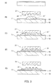
本発明のインプリント方法は、所望の形状の転写形状部を有するモールドと転写基材との間に被加工物を介在させ、被加工物に転写形状部の形状を転写するものである。
図3は、本発明のインプリント方法の一実施形態を説明するための工程図である。
本発明では、まず、密着層形成工程にて、基材12に密着層13を形成して転写基材11を作製する(図3(A))。この基材12は、上述の本発明の転写基材1を構成する基材2として挙げたものと同様のものを使用することができる。また、密着層13は、1個の加水分解性基と2個の不活性基とを有する4価の原子と該原子に結合した反応性官能基とを1分子中に有する化合物を含有する密着剤を、基材12に接触させ、その後、洗浄することにより形成することができる。
[Imprint method]
Next, the imprint method of the present invention will be described.
In the imprint method of the present invention, a workpiece is interposed between a mold having a transfer shape portion having a desired shape and a transfer substrate, and the shape of the transfer shape portion is transferred to the workpiece.
FIG. 3 is a process diagram for explaining an embodiment of the imprint method of the present invention.
In the present invention, first, in the adhesion layer forming step, the
基材12への密着剤の接触は、例えば、化学蒸着法、ウェットプロセス等により行うことができる。ウェットプロセスとしては、スピンコート法、浸漬コート法、ディッピング法等を挙げることができ、このようなウェットプロセスは、簡便にできる方法として好ましい。
基材12に接触された密着剤は、4価の原子に結合している1個の加水分解性基が加水分解を受け、基材12の表面の水酸基が存在する反応点との結合(水素結合を経て、酸素原子を介した共有結合を形成)がなされる。また、4価の原子は2個の不活性基を有しているので、基材12の表面に結合した4価の原子が、他の分子の4価の原子と縮合反応を生じることが抑制される。したがって、基材と未反応の密着剤は、例えば、二量体を形成することはあっても、基材12の表面に結合した4価の原子とは結合していないため、洗浄によって除去される。これにより、例えば、図4に示すように、基材12の段差部分12Aにおいても不要な密着剤による密着層の厚みの増大(図4に鎖線で示した盛り上がり部位)を抑制することができ、表面に反応性官能基が位置する均一な厚みの密着層13を形成することができる。基材12と未反応の密着剤を除去するための洗浄は、例えば、メチルアルコール、エチルアルコール、イソプロピルアルコール、ベンゼン、トルエン、キシレン、アセトン、酢酸エチル、テトラヒドロフラン、メチルエチルケトン、メチルイソブチルケトン、メチルセロソルブ等の極性溶媒を使用して行うことができる。また、洗浄方法としては、スピンコート法、浸漬コート法、ディッピング法等を挙げることができる。尚、密着剤の接触前、あるいは、接触後に基材12を加熱することにより、密着剤と基材12との反応を促進してもよい。
このような密着層形成工程において使用する密着剤は、上記の本発明の密着剤であってよい。
The contact of the adhesive with the
The adhesive that is in contact with the
The adhesive used in such an adhesive layer forming step may be the adhesive of the present invention described above.
次いで、充填工程において、転写基材11の密着層13上に被加工物31′を供給し(図3(B))、転写形状部22を有するモールド21と密着層13との間に被加工物31′が介在するようしてモールド21と転写基材11とを近接させ、被加工物31′をモールド21の転写形状部22に充填する(図3(C))。尚、上記のモールド21の転写形状部22への被加工物31′の充填は、モールド21上に被加工物31′を供給し、この被加工物31′に転写基材11の密着層13を押し当てて行ってもよい。
モールド21は、被加工物31′が光硬化性樹脂である場合に、被加工物31′を硬化させるための照射光を透過可能な透明基材を用いて形成することができ、例えば、石英ガラス、珪酸系ガラス、フッ化カルシウム、フッ化マグネシウム、アクリルガラス等、あるいは、これらの任意の積層材を用いることができる。モールド21が有する転写形状部22は、図示例では凹部が形成された凹凸構造を有しているが、これに限定されるものではなく、形状、寸法は任意に設定することができる。また、使用するモールド21は、転写形状部22が位置する部位が周囲に対して凸構造となった、いわゆるメサ構造であってもよい。
Next, in the filling step, a
The
次に、硬化工程において、転写基材11とモールド21との間に介在する被加工物31′を硬化させて被加工物31とする(図3(D))。この被加工物31は、密着層13の表面に位置する反応性官能基と反応し結合して、密着層13に確実に保持される。このような硬化工程では、被加工物31′が光硬化性の樹脂である場合、モールド21側から光照射を行って硬化処理を施すことができる。また、転写基材11が照射光を透過可能である場合には、転写基材11側から光照射を行って被加工物31′を硬化させてもよい。
次いで、離型工程において、被加工物31からモールド21を引き離す(図3(E))。これにより、被加工物31にパターン形成(モールド21の転写形状部22の転写)が行われる。本発明では、被加工物31が密着層13を介して転写基材11の基材12に確実に保持されているので、モールド21への被加工物31の付着による転写欠陥が防止され、高精度のパターン形成を行うことが可能である。
Next, in the curing step, the
Next, in the mold release step, the
また、図示していないが、上記の離型工程の後、被加工物31の残膜部分を、その下部に位置する密着層13とともに除去して基材12の表面を露出させ、この状態で残存する被加工物31をレジストパターンとして基材12の表面にエッチングを施し、基材12に凹凸構造のパターンを形成してもよい。この場合、密着層13の厚みが不均一であると、密着層13を含めた被加工物31の残膜部分の厚みが不均一になり、レジストパターンの精度が低下し、その結果、レジストパターンを介してエッチングにより基材12に形成されるパターンの精度低下を招くことになる。本発明のインプリント方法によれば、密着層の厚みが均一であるため、高精度のパターン形成を行うことができる。
Although not shown in the figure, after the mold release step, the remaining film portion of the
また、このような本発明のインプリント方法は、密着層形成工程において使用する密着剤が加水分解を受け難く、ケイ素が複数の加水分解性基を有するシランカップリング剤に比べて、保存安定性に優れるため、製造工程管理が容易で、パターン形成におけるコスト低減が可能である。
上述の本発明のインプリント方法の実施形態は例示であり、本発明はこれに限定されるものではない。
In addition, the imprint method of the present invention is such that the adhesion agent used in the adhesion layer forming step is less susceptible to hydrolysis, and the storage stability is higher than that of a silane coupling agent in which silicon has a plurality of hydrolyzable groups. Therefore, manufacturing process management is easy, and the cost for pattern formation can be reduced.
The above-described embodiment of the imprint method of the present invention is an exemplification, and the present invention is not limited to this.
次に、より具体的な実施例を示して本発明を更に詳細に説明する。
[実施例1]
<密着層形成工程>
基材として、シリコンウエハ(直径150mm)を準備した。この基材は、一方の面の中央部に26mm×32mmの凸状平坦面を有し、この凸状平坦面における基材厚みは0.625mmであり、その周囲の基材厚み0.595mmとの間に0.03mmの段差を有するものであった。
Next, the present invention will be described in more detail by showing more specific examples.
[Example 1]
<Adhesion layer forming step>
A silicon wafer (diameter 150 mm) was prepared as a substrate. This base material has a convex flat surface of 26 mm × 32 mm at the center of one surface, and the base material thickness in this convex flat surface is 0.625 mm, and the base material thickness of the surroundings is 0.595 mm. There was a step of 0.03 mm in between.
また、密着剤Aとして、(3−アクリロキシプロピル)ジメチルメトキシシラン(Gelest社製)を準備した。この密着剤Aについて、下記の条件でNMR分光法により1H−NMRおよび29Si−NMRの経時変化を測定することにより、密着剤に経時的に生じる加水分解、脱水縮合の程度を判断し、保存安定性を評価して、結果を下記の表1に示した。
(NMR分光法の測定条件)
日本電子(株)製 JNM−LA400WBを用いて1H−NMRおよび29Si
−NMRを測定し、シランカップリング剤重縮合の反応過程を解析した。共鳴
周波数は、400MHzおよび79.3MHzとし、外部基準としてテトラメ
チルシランを用いた。
(保存安定性の評価基準)
○:密着剤の容器を開封し、1ヶ月でメタノールが生成されておらず、保
存安定性は良好
×:密着剤の容器を開封し、1ヶ月でメタノールが生成されており、保存
安定性は不良
Further, (3-acryloxypropyl) dimethylmethoxysilane (manufactured by Gelest) was prepared as the adhesive A. About this adhesion agent A, the degree of hydrolysis and dehydration condensation occurring over time in the adhesion agent is determined by measuring the time course of 1 H-NMR and 29 Si-NMR by NMR spectroscopy under the following conditions: The storage stability was evaluated and the results are shown in Table 1 below.
(Measurement conditions for NMR spectroscopy)
1 J-NMR and 29 Si using JNM-LA400WB manufactured by JEOL Ltd.
-NMR was measured and the reaction process of silane coupling agent polycondensation was analyzed. The resonance frequencies were 400 MHz and 79.3 MHz, and tetramethylsilane was used as an external reference.
(Evaluation criteria for storage stability)
○: The container for the adhesive was opened and no methanol was produced in one month.
Good stability
X: The container of the adhesive was opened, and methanol was produced in one month, and stored
Stability is poor
上記の密着剤Aを基材の凸状平坦面側にスピンコート法により塗布して接触させ、その後、洗浄液としてイソプロピルアルコールを用いてスピンコート法で基材の密着剤塗布面を洗浄した。その後、基材を80℃に加熱して10分間保持した。これにより、凸状平坦面に密着層を備えた転写基材を作製した。
また、下記の条件で接触角の経時変化を測定することにより、形成後の密着層に経時的に生じる表面の劣化の程度を判断し、保存安定性を評価して、結果を下記の表1に示した。
(接触角の測定条件)
密着層上にマイクロシリンジから水滴を滴下し、10秒後に協和界面科学(株)
製 DM−700型を用いて水に対する接触角を測定した。
(保存安定性の評価基準)
○:密着層形成後、1週間の接触角変化が2°以下であり、保存安定性は
良好
×:密着層形成後、1週間の接触角変化が2°を超えるものであり、保存
安定性は不良
The adhesive agent A was applied to and contacted with the convex flat surface side of the substrate by a spin coating method, and then the adhesive agent-coated surface of the substrate was cleaned by a spin coating method using isopropyl alcohol as a cleaning liquid. Thereafter, the substrate was heated to 80 ° C. and held for 10 minutes. This produced the transfer base material provided with the contact | adherence layer on the convex-shaped flat surface.
Further, by measuring the change in contact angle with time under the following conditions, the degree of surface deterioration that occurs over time in the formed adhesion layer was judged, storage stability was evaluated, and the results are shown in Table 1 below. It was shown to.
(Contact angle measurement conditions)
A drop of water is dropped from the microsyringe onto the adhesive layer, and 10 seconds later, Kyowa Interface Science Co., Ltd.
The contact angle with respect to water was measured using DM-700 type.
(Evaluation criteria for storage stability)
○: After the formation of the adhesion layer, the contact angle change for one week is 2 ° or less, and the storage stability is
Good
×: After the formation of the adhesion layer, the change in contact angle for 1 week exceeds 2 °, and storage
Stability is poor
作製した転写基材の密着層の表面における凸部(密着剤の凝集により生成したものと考えられる)の存在の有無を、下記の条件で原子間力顕微鏡(AFM)により観察、評価して、結果を下記の表1に示した。
(原子間力顕微鏡による評価条件)
原子間力顕微鏡(SIIナノテクノロジー(株)製 L−trace)を用い、
密着層の0.03mm×0.03mmの領域を測定し、高さ5nm以上の凸部の
存在有無を評価した。高さ5nm以上の凸部は、転写欠陥の原因となりうるため
である。
(密着層表面の評価基準)
○:高さ5nm以上の凸部が存在しない
×:高さ5nm以上の凸部が存在する
The presence or absence of a convex portion (which is considered to have been generated by aggregation of the adhesive) on the surface of the adhesion layer of the produced transfer substrate was observed and evaluated with an atomic force microscope (AFM) under the following conditions. The results are shown in Table 1 below.
(Evaluation conditions by atomic force microscope)
Using an atomic force microscope (L-trace made by SII Nanotechnology),
An area of 0.03 mm × 0.03 mm of the adhesion layer was measured, and the presence / absence of a projection having a height of 5 nm or more was evaluated. This is because convex portions having a height of 5 nm or more can cause transfer defects.
(Evaluation criteria for adhesion layer surface)
○: There is no convex part with a height of 5 nm or more
X: Convex part with a height of 5 nm or more exists
<充填工程>
厚み6.35mmの石英ガラス(40mm×40mm)の凹凸構造パターンの無い平坦なモールドを準備した。
また、被加工物として下記組成の光硬化性樹脂を準備し、この被加工物の液滴を、上記の転写基材の密着層上の5×5箇所(計25箇所)に0.5mmピッチで供給し、その後、インプリント装置の基板ステージに載置した。次に、被加工物に上記のモールドを押し込み、転写形状部の凹凸構造に被加工物を充填した。
(光硬化性樹脂の組成)
・イソボルニルアクリレート … 38重量%
・エチレングリコールジアクリレート … 20重量%
・ブチルアクリレート … 38重量%
・2−ヒドロキシ−2−メチル−1−フェニル−プロパン−1−オン
… 2重量%
・2−ペルフルオロデシルエチルアクリレート … 1重量%
・メチルペルフルオロオクタノレート … 1重量%
<Filling process>
A flat mold without a concavo-convex structure pattern of quartz glass (40 mm × 40 mm) having a thickness of 6.35 mm was prepared.
In addition, a photocurable resin having the following composition was prepared as a workpiece, and droplets of this workpiece were placed at a pitch of 0.5 mm at 5 × 5 locations (a total of 25 locations) on the adhesion layer of the transfer substrate. And then placed on the substrate stage of the imprint apparatus. Next, the mold was pushed into the workpiece, and the uneven structure of the transfer shape portion was filled with the workpiece.
(Composition of photocurable resin)
・ Isobornyl acrylate: 38% by weight
・ Ethylene glycol diacrylate: 20% by weight
・ Butyl acrylate: 38% by weight
2-Hydroxy-2-methyl-1-phenyl-propan-1-one
... 2% by weight
・ 2-Perfluorodecylethyl acrylate: 1% by weight
・ Methyl perfluorooctanolate: 1% by weight
<硬化工程>
モールドと転写基材との間に被加工物である光硬化性樹脂が存在する状態で、インプリント装置の照明光学系により紫外線をモールド側から100mJ/cm2照射した。これにより、光硬化性樹脂を硬化させた。
<離型工程>
次に、硬化した被加工物からモールドを引き離し、転写面を形成した。
<Curing process>
In the state where the photocurable resin as the workpiece exists between the mold and the transfer substrate, ultraviolet rays were irradiated from the mold side by 100 mJ / cm 2 by the illumination optical system of the imprint apparatus. Thereby, the photocurable resin was cured.
<Release process>
Next, the mold was pulled away from the cured workpiece to form a transfer surface.
[実施例2]
密着剤Bとして、1,3−ビス(3−アクリロキシメチル)テトラメチルジシラザン(信越化学工業(株)製)を準備し、この密着剤Bを密着剤Aに代えて使用した他は、実施例1と同様にして、被加工物にモールドの平坦面を転写形成した。
使用した密着剤Bの保管安定性を、実施例1と同様に評価して、結果を下記の表1に示した。
また、作製した転写基材の密着層の表面における凸部の存在の有無を、実施例1と同様に観察して、結果を下記の表1に示した。
[Example 2]
As the adhesive B, 1,3-bis (3-acryloxymethyl) tetramethyldisilazane (manufactured by Shin-Etsu Chemical Co., Ltd.) was prepared, and this adhesive B was used instead of the adhesive A. In the same manner as in Example 1, the flat surface of the mold was transferred and formed on the workpiece.
The storage stability of the used adhesive B was evaluated in the same manner as in Example 1, and the results are shown in Table 1 below.
Moreover, the presence or absence of the convex part in the surface of the adhesion layer of the produced transfer substrate was observed in the same manner as in Example 1, and the results are shown in Table 1 below.
[比較例1]
密着剤Cとして、(3−アクリロキシメチル)トリメトキシシラン(Gelest社製)を準備し、この密着剤Cを密着剤Aに代えて使用した他は、実施例1と同様にして、被加工物にモールドの平坦面を転写形成した。
使用した密着剤Cの保管安定性を、実施例1と同様に評価して、結果を下記の表1に示した。
また、作製した転写基材の密着層の表面における凸部の存在の有無を、実施例1と同様に観察して、結果を下記の表1に示した。
[Comparative Example 1]
As (3), (3-acryloxymethyl) trimethoxysilane (manufactured by Gelest) was prepared, and this adhesive C was used in place of the adhesive A. The flat surface of the mold was transferred to the object.
The storage stability of the used adhesive C was evaluated in the same manner as in Example 1, and the results are shown in Table 1 below.
Moreover, the presence or absence of the convex part in the surface of the adhesion layer of the produced transfer substrate was observed in the same manner as in Example 1, and the results are shown in Table 1 below.
[比較例2]
密着層形成工程において、洗浄液を用いた洗浄を実施しない他は、実施例1と同様にして、被加工物にモールドの平坦面を転写形成した。
作製した転写基材の密着層の表面における凸部の存在の有無を、実施例1と同様に観察して、結果を下記の表1に示した。
[Comparative Example 2]
In the adhesion layer forming step, the flat surface of the mold was transferred and formed on the workpiece in the same manner as in Example 1 except that the cleaning using the cleaning liquid was not performed.
The presence or absence of protrusions on the surface of the adhesion layer of the produced transfer substrate was observed in the same manner as in Example 1, and the results are shown in Table 1 below.
表1に示されるように、本発明の密着剤である密着剤A、Bは、保管安定性に優れることが確認された。また、実施例1、2において、密着剤A、Bを用いて密着層を形成して作製した本発明の転写基材では、密着層の表面に凸部の存在が確認されず、また、基材の段差部位での密着層の盛り上がりがないことが確認された。このことから、基材表面に結合したケイ素原子と他の分子のケイ素原子との間で、縮合反応による結合を生じることが抑制されていることが確認され、また、洗浄によって、基材と未反応の密着剤が確実に除去されていることが確認された。さらに、実施例1、2において形成された転写面は、いずれも転写欠陥が発生せず、本発明のインプリント方法による良好なパターン形成(モールドの平坦面の転写)が行われたことが確認された。
これに対して、密着剤Cは、保管安定性が劣るものであった。また、比較例1において、密着剤Cを用いて密着層を形成して作製した転写基材、および、比較例2において洗浄を行わずに密着層を形成して作製した転写基材では、密着層の表面に凸部の存在が確認された。
As shown in Table 1, it was confirmed that the adhesives A and B, which are the adhesives of the present invention, are excellent in storage stability. Further, in Examples 1 and 2, in the transfer base material of the present invention produced by forming the adhesion layer using the adhesion agents A and B, the presence of convex portions on the surface of the adhesion layer was not confirmed. It was confirmed that there was no swell of the adhesion layer at the level difference part of the material. This confirms that the formation of a bond due to the condensation reaction between the silicon atom bonded to the surface of the substrate and the silicon atom of other molecules is suppressed. It was confirmed that the reaction adhesive was removed reliably. Furthermore, it was confirmed that the transfer surfaces formed in Examples 1 and 2 did not cause any transfer defects, and good pattern formation (transfer of the flat surface of the mold) was performed by the imprint method of the present invention. It was done.
In contrast, the adhesive C was inferior in storage stability. In Comparative Example 1, the transfer substrate produced by forming an adhesion layer using the adhesion agent C, and the transfer substrate produced by forming an adhesion layer without cleaning in Comparative Example 2, Presence of protrusions was confirmed on the surface of the layer.
インプリント技術を用いたパターン形成、微細加工に利用可能である。 It can be used for pattern formation and fine processing using imprint technology.
1,11…転写基材
2,12…基材
3,13…密着層
4…濡れ性変化層
21…モールド
22…転写形状部
31′…被加工物
31…硬化した被加工物
DESCRIPTION OF
Claims (9)
基材に密着層を形成して転写基材を作製する密着層形成工程と、
前記モールドと前記密着層との間に前記被加工物が介在するようして前記モールドと前記転写基材とを近接させ前記被加工物を前記転写形状部に充填する充填工程と、
前記被加工物を硬化させる硬化工程と、
前記被加工物から前記モールドを引き離す離型工程と、を有し、
前記密着層形成工程は、1個の加水分解性基と2個の不活性基とを有する4価の原子と該原子に結合した反応性官能基とを1分子中に有する化合物を含有する密着剤を、前記基材に接触させ、その後、洗浄する工程を有し、高さ5nm以上の凸部が存在しない密着層を形成するものであることを特徴とするインプリント方法。 In an imprint method in which a workpiece is interposed between a mold having a transfer shape portion of a desired shape and a transfer substrate, and the shape of the transfer shape portion is transferred to the workpiece.
An adhesion layer forming step of forming an adhesion layer on the substrate to produce a transfer substrate;
A filling step of filling the transfer shape portion with the workpiece by bringing the mold and the transfer base material close to each other so that the workpiece is interposed between the mold and the adhesion layer;
A curing step for curing the workpiece;
A mold release step of separating the mold from the workpiece,
The adhesion layer forming step comprises adhesion comprising a compound having a tetravalent atom having one hydrolyzable group and two inactive groups and a reactive functional group bonded to the atom in one molecule. agents, into contact with the substrate, then, imprinting wherein the have a step of washing, and forms an adhesive layer projecting portion of the above height of 5nm is not present.
密着層は、酸素原子を介して前記基材に結合するとともに2個の不活性基とを有する4価の原子と、該原子に結合した反応性官能基と、を有し、高さ5nm以上の凸部が存在しないことを特徴とする転写基材。 In a transfer substrate for imprint comprising a substrate and an adhesion layer located on the substrate,
Adhesion layer, and the tetravalent atom having a two inert radicals as well as coupled to the substrate via an oxygen atom, possess a reactive functional group attached to the atom, the, 5 nm or more height A transfer substrate characterized in that there is no convex part .
Priority Applications (4)
| Application Number | Priority Date | Filing Date | Title |
|---|---|---|---|
| JP2010236181A JP5218521B2 (en) | 2010-10-21 | 2010-10-21 | Imprint method and transfer substrate and adhesive used therefor |
| US13/880,507 US9375871B2 (en) | 2010-10-21 | 2011-10-07 | Imprint process, and transfer substrate and adhesive used therewith |
| PCT/JP2011/073751 WO2012053458A1 (en) | 2010-10-21 | 2011-10-07 | Imprinting method, and bonding agent and transfer substrate used in same |
| KR1020137008150A KR101797233B1 (en) | 2010-10-21 | 2011-10-07 | Imprinting method, and bonding agent and transfer substrate used in same |
Applications Claiming Priority (1)
| Application Number | Priority Date | Filing Date | Title |
|---|---|---|---|
| JP2010236181A JP5218521B2 (en) | 2010-10-21 | 2010-10-21 | Imprint method and transfer substrate and adhesive used therefor |
Publications (3)
| Publication Number | Publication Date |
|---|---|
| JP2012086484A JP2012086484A (en) | 2012-05-10 |
| JP2012086484A5 JP2012086484A5 (en) | 2013-02-28 |
| JP5218521B2 true JP5218521B2 (en) | 2013-06-26 |
Family
ID=45975171
Family Applications (1)
| Application Number | Title | Priority Date | Filing Date |
|---|---|---|---|
| JP2010236181A Active JP5218521B2 (en) | 2010-10-21 | 2010-10-21 | Imprint method and transfer substrate and adhesive used therefor |
Country Status (4)
| Country | Link |
|---|---|
| US (1) | US9375871B2 (en) |
| JP (1) | JP5218521B2 (en) |
| KR (1) | KR101797233B1 (en) |
| WO (1) | WO2012053458A1 (en) |
Families Citing this family (7)
| Publication number | Priority date | Publication date | Assignee | Title |
|---|---|---|---|---|
| JP2014093385A (en) * | 2012-11-02 | 2014-05-19 | Fujifilm Corp | Method of manufacturing adhesion film for imprint and method of forming pattern |
| JP2015028978A (en) * | 2013-07-30 | 2015-02-12 | 大日本印刷株式会社 | Foreign matter detection method, imprint method, and imprint system |
| JP6244742B2 (en) * | 2013-08-26 | 2017-12-13 | 大日本印刷株式会社 | Film inspection method, imprint method, pattern structure manufacturing method, imprint mold, imprint transfer substrate, and imprint apparatus |
| CN106537557B (en) | 2014-07-08 | 2019-06-18 | 佳能株式会社 | Adhesion layer composition passes through the method that nano impression forms film, the manufacturing method of optical module, circuit board and electronic equipment |
| JP6712673B2 (en) * | 2017-02-28 | 2020-06-24 | 富士フイルム株式会社 | Adhesive film forming composition for imprint, adhesive film, laminate, method for producing cured product pattern and method for producing circuit board |
| TW201900704A (en) | 2017-04-11 | 2019-01-01 | 日商富士軟片股份有限公司 | Composition, adhesion film, laminate, method for producing cured pattern, and method for manufacturing circuit board |
| EP3929658A1 (en) * | 2020-06-23 | 2021-12-29 | Koninklijke Philips N.V. | Imprinting method and patterned layer |
Family Cites Families (22)
| Publication number | Priority date | Publication date | Assignee | Title |
|---|---|---|---|---|
| JP2938722B2 (en) * | 1993-07-12 | 1999-08-25 | 信越化学工業株式会社 | Acrylic-functional silane compound polymerization inhibitor |
| US5908530A (en) * | 1995-05-18 | 1999-06-01 | Obsidian, Inc. | Apparatus for chemical mechanical polishing |
| KR100396469B1 (en) * | 2001-06-29 | 2003-09-02 | 삼성전자주식회사 | Method of forming the gate electrode in semiconductor device and Method of manufacturing the non-volatile memory device comprising the same |
| US6899596B2 (en) * | 2002-02-22 | 2005-05-31 | Agere Systems, Inc. | Chemical mechanical polishing of dual orientation polycrystalline materials |
| JP4154595B2 (en) | 2003-05-28 | 2008-09-24 | ダイキン工業株式会社 | Imprint mold and method for manufacturing the same |
| US7635263B2 (en) * | 2005-01-31 | 2009-12-22 | Molecular Imprints, Inc. | Chucking system comprising an array of fluid chambers |
| JP2006255811A (en) * | 2005-03-15 | 2006-09-28 | National Institute For Materials Science | Monomolecular film forming method |
| US8808808B2 (en) * | 2005-07-22 | 2014-08-19 | Molecular Imprints, Inc. | Method for imprint lithography utilizing an adhesion primer layer |
| US8846195B2 (en) | 2005-07-22 | 2014-09-30 | Canon Nanotechnologies, Inc. | Ultra-thin polymeric adhesion layer |
| US7759407B2 (en) | 2005-07-22 | 2010-07-20 | Molecular Imprints, Inc. | Composition for adhering materials together |
| US8557351B2 (en) | 2005-07-22 | 2013-10-15 | Molecular Imprints, Inc. | Method for adhering materials together |
| US7766640B2 (en) * | 2005-08-12 | 2010-08-03 | Hewlett-Packard Development Company, L.P. | Contact lithography apparatus, system and method |
| JP4287421B2 (en) * | 2005-10-13 | 2009-07-01 | 株式会社ルネサステクノロジ | Manufacturing method of semiconductor device |
| JP2007144995A (en) | 2005-10-25 | 2007-06-14 | Dainippon Printing Co Ltd | Mold for photo-curable nano-imprinting and its manufacturing method |
| US20090325323A1 (en) * | 2006-07-18 | 2009-12-31 | Jsr Corporation | Aqueous dispersion for chemical mechanical polishing, production method thereof, and chemical mechanical polishing method |
| US7768628B2 (en) * | 2006-10-12 | 2010-08-03 | Hewlett-Packard Development Company, L.P. | Contact lithography apparatus and method |
| JP4940884B2 (en) * | 2006-10-17 | 2012-05-30 | 大日本印刷株式会社 | Method for producing pattern forming body |
| JP5037243B2 (en) | 2007-07-06 | 2012-09-26 | 富士フイルム株式会社 | Interfacial binder, resist composition containing the interfacial binder, laminate for forming a magnetic recording medium having a layer comprising the interfacial binder, a method for producing a magnetic recording medium using the interfacial binder, and Magnetic recording medium manufactured by the manufacturing method |
| JP5374949B2 (en) | 2007-08-21 | 2013-12-25 | 信越化学工業株式会社 | Process for producing radiation-polymerizable functional group-containing organosilylamine and radiation-polymerizable functional group-containing organosilylamine |
| US20100052216A1 (en) * | 2008-08-29 | 2010-03-04 | Yong Hyup Kim | Nano imprint lithography using an elastic roller |
| US20100252103A1 (en) * | 2009-04-03 | 2010-10-07 | Chiu-Lin Yao | Photoelectronic element having a transparent adhesion structure and the manufacturing method thereof |
| KR101708256B1 (en) * | 2009-07-29 | 2017-02-20 | 닛산 가가쿠 고교 가부시키 가이샤 | Composition for forming resist underlayer film for nanoimprint lithography |
-
2010
- 2010-10-21 JP JP2010236181A patent/JP5218521B2/en active Active
-
2011
- 2011-10-07 US US13/880,507 patent/US9375871B2/en active Active
- 2011-10-07 WO PCT/JP2011/073751 patent/WO2012053458A1/en active Application Filing
- 2011-10-07 KR KR1020137008150A patent/KR101797233B1/en active IP Right Grant
Also Published As
| Publication number | Publication date |
|---|---|
| US20130270741A1 (en) | 2013-10-17 |
| WO2012053458A1 (en) | 2012-04-26 |
| JP2012086484A (en) | 2012-05-10 |
| KR101797233B1 (en) | 2017-11-13 |
| KR20130123376A (en) | 2013-11-12 |
| US9375871B2 (en) | 2016-06-28 |
Similar Documents
| Publication | Publication Date | Title |
|---|---|---|
| JP5218521B2 (en) | Imprint method and transfer substrate and adhesive used therefor | |
| JP5399374B2 (en) | Method for imprint lithography utilizing an adhesive primer layer | |
| JP6139646B2 (en) | Photomask substrate with adhesion auxiliary layer and method of manufacturing photomask substrate with adhesion auxiliary layer | |
| TWI515513B (en) | Resist underlayer film forming composition for nanoimprinting | |
| JP5879086B2 (en) | Replica mold for nanoimprint | |
| US8415010B2 (en) | Nano-imprint lithography stack with enhanced adhesion between silicon-containing and non-silicon containing layers | |
| JP5678728B2 (en) | Mold and manufacturing method thereof | |
| JP5891814B2 (en) | Pattern structure manufacturing method and pattern forming substrate used therefor | |
| TWI676865B (en) | Curable composition, photoresist material, photoresist film, laminate, pattern forming method, and molded body | |
| US8344039B2 (en) | Three-dimensional pattern forming material | |
| US8641941B2 (en) | Photocatalytic reactions in nano-imprint lithography processes | |
| JP5871203B1 (en) | Oxygen plasma etching resist material, resist film, and laminate using the same | |
| JP5362186B2 (en) | Resin composition for nanoimprint | |
| TW201410442A (en) | Method for manufacturing article having fine pattern on surface thereof | |
| KR20150090073A (en) | Method for producing microstructure and photocurable composition for nanoimprinting | |
| JP6008628B2 (en) | Pattern production method using photocurable nanoimprinting composition | |
| US20110165412A1 (en) | Adhesion layers in nanoimprint lithograhy | |
| WO2020203472A1 (en) | Photocurable resin composition for imprinting, production method for photocurable resin composition for imprinting, and production method for pattern-formed body | |
| JP2012183753A (en) | Nanoimprinting method | |
| JP2006106449A (en) | Inorganic micropattern organizer and manufacturing method thereof | |
| TW202216801A (en) | Primer layer forming composition for imprint | |
| TWI391418B (en) | Nano-imprint resist and nanoimprinting lithography method using the same | |
| Pina | Novel organosilicone materials and patterning techniques for nanoimprint lithography | |
| Ell | A fundamental study of the modification of elastomeric poly (dimethylsiloxane) and silicon surfaces using polymers and their applications in patterning |
Legal Events
| Date | Code | Title | Description |
|---|---|---|---|
| A521 | Request for written amendment filed |
Free format text: JAPANESE INTERMEDIATE CODE: A523 Effective date: 20120531 |
|
| A521 | Request for written amendment filed |
Free format text: JAPANESE INTERMEDIATE CODE: A523 Effective date: 20130110 |
|
| A621 | Written request for application examination |
Free format text: JAPANESE INTERMEDIATE CODE: A621 Effective date: 20130110 |
|
| A871 | Explanation of circumstances concerning accelerated examination |
Free format text: JAPANESE INTERMEDIATE CODE: A871 Effective date: 20130110 |
|
| TRDD | Decision of grant or rejection written | ||
| A975 | Report on accelerated examination |
Free format text: JAPANESE INTERMEDIATE CODE: A971005 Effective date: 20130129 |
|
| A01 | Written decision to grant a patent or to grant a registration (utility model) |
Free format text: JAPANESE INTERMEDIATE CODE: A01 Effective date: 20130205 |
|
| A61 | First payment of annual fees (during grant procedure) |
Free format text: JAPANESE INTERMEDIATE CODE: A61 Effective date: 20130218 |
|
| FPAY | Renewal fee payment (event date is renewal date of database) |
Free format text: PAYMENT UNTIL: 20160315 Year of fee payment: 3 |
|
| R150 | Certificate of patent or registration of utility model |
Ref document number: 5218521 Country of ref document: JP Free format text: JAPANESE INTERMEDIATE CODE: R150 Free format text: JAPANESE INTERMEDIATE CODE: R150 |