JP5215244B2 - Semiconductor device - Google Patents
Semiconductor device Download PDFInfo
- Publication number
- JP5215244B2 JP5215244B2 JP2009145430A JP2009145430A JP5215244B2 JP 5215244 B2 JP5215244 B2 JP 5215244B2 JP 2009145430 A JP2009145430 A JP 2009145430A JP 2009145430 A JP2009145430 A JP 2009145430A JP 5215244 B2 JP5215244 B2 JP 5215244B2
- Authority
- JP
- Japan
- Prior art keywords
- semiconductor chip
- semiconductor chips
- semiconductor
- conductive
- stacked body
- Prior art date
- Legal status (The legal status is an assumption and is not a legal conclusion. Google has not performed a legal analysis and makes no representation as to the accuracy of the status listed.)
- Expired - Fee Related
Links
Images


Classifications
-
- H—ELECTRICITY
- H01—ELECTRIC ELEMENTS
- H01L—SEMICONDUCTOR DEVICES NOT COVERED BY CLASS H10
- H01L23/00—Details of semiconductor or other solid state devices
- H01L23/48—Arrangements for conducting electric current to or from the solid state body in operation, e.g. leads, terminal arrangements ; Selection of materials therefor
- H01L23/488—Arrangements for conducting electric current to or from the solid state body in operation, e.g. leads, terminal arrangements ; Selection of materials therefor consisting of soldered or bonded constructions
- H01L23/498—Leads, i.e. metallisations or lead-frames on insulating substrates, e.g. chip carriers
- H01L23/49811—Additional leads joined to the metallisation on the insulating substrate, e.g. pins, bumps, wires, flat leads
-
- H—ELECTRICITY
- H01—ELECTRIC ELEMENTS
- H01L—SEMICONDUCTOR DEVICES NOT COVERED BY CLASS H10
- H01L23/00—Details of semiconductor or other solid state devices
- H01L23/28—Encapsulations, e.g. encapsulating layers, coatings, e.g. for protection
- H01L23/31—Encapsulations, e.g. encapsulating layers, coatings, e.g. for protection characterised by the arrangement or shape
- H01L23/3107—Encapsulations, e.g. encapsulating layers, coatings, e.g. for protection characterised by the arrangement or shape the device being completely enclosed
- H01L23/3121—Encapsulations, e.g. encapsulating layers, coatings, e.g. for protection characterised by the arrangement or shape the device being completely enclosed a substrate forming part of the encapsulation
-
- H—ELECTRICITY
- H01—ELECTRIC ELEMENTS
- H01L—SEMICONDUCTOR DEVICES NOT COVERED BY CLASS H10
- H01L24/00—Arrangements for connecting or disconnecting semiconductor or solid-state bodies; Methods or apparatus related thereto
- H01L24/01—Means for bonding being attached to, or being formed on, the surface to be connected, e.g. chip-to-package, die-attach, "first-level" interconnects; Manufacturing methods related thereto
- H01L24/18—High density interconnect [HDI] connectors; Manufacturing methods related thereto
- H01L24/23—Structure, shape, material or disposition of the high density interconnect connectors after the connecting process
- H01L24/24—Structure, shape, material or disposition of the high density interconnect connectors after the connecting process of an individual high density interconnect connector
-
- H—ELECTRICITY
- H01—ELECTRIC ELEMENTS
- H01L—SEMICONDUCTOR DEVICES NOT COVERED BY CLASS H10
- H01L24/00—Arrangements for connecting or disconnecting semiconductor or solid-state bodies; Methods or apparatus related thereto
- H01L24/80—Methods for connecting semiconductor or other solid state bodies using means for bonding being attached to, or being formed on, the surface to be connected
- H01L24/82—Methods for connecting semiconductor or other solid state bodies using means for bonding being attached to, or being formed on, the surface to be connected by forming build-up interconnects at chip-level, e.g. for high density interconnects [HDI]
-
- H—ELECTRICITY
- H01—ELECTRIC ELEMENTS
- H01L—SEMICONDUCTOR DEVICES NOT COVERED BY CLASS H10
- H01L24/00—Arrangements for connecting or disconnecting semiconductor or solid-state bodies; Methods or apparatus related thereto
- H01L24/91—Methods for connecting semiconductor or solid state bodies including different methods provided for in two or more of groups H01L24/80 - H01L24/90
-
- H—ELECTRICITY
- H01—ELECTRIC ELEMENTS
- H01L—SEMICONDUCTOR DEVICES NOT COVERED BY CLASS H10
- H01L25/00—Assemblies consisting of a plurality of individual semiconductor or other solid state devices ; Multistep manufacturing processes thereof
- H01L25/03—Assemblies consisting of a plurality of individual semiconductor or other solid state devices ; Multistep manufacturing processes thereof all the devices being of a type provided for in the same subgroup of groups H01L27/00 - H01L33/00, or in a single subclass of H10K, H10N, e.g. assemblies of rectifier diodes
- H01L25/04—Assemblies consisting of a plurality of individual semiconductor or other solid state devices ; Multistep manufacturing processes thereof all the devices being of a type provided for in the same subgroup of groups H01L27/00 - H01L33/00, or in a single subclass of H10K, H10N, e.g. assemblies of rectifier diodes the devices not having separate containers
- H01L25/065—Assemblies consisting of a plurality of individual semiconductor or other solid state devices ; Multistep manufacturing processes thereof all the devices being of a type provided for in the same subgroup of groups H01L27/00 - H01L33/00, or in a single subclass of H10K, H10N, e.g. assemblies of rectifier diodes the devices not having separate containers the devices being of a type provided for in group H01L27/00
- H01L25/0657—Stacked arrangements of devices
-
- H—ELECTRICITY
- H01—ELECTRIC ELEMENTS
- H01L—SEMICONDUCTOR DEVICES NOT COVERED BY CLASS H10
- H01L2224/00—Indexing scheme for arrangements for connecting or disconnecting semiconductor or solid-state bodies and methods related thereto as covered by H01L24/00
- H01L2224/01—Means for bonding being attached to, or being formed on, the surface to be connected, e.g. chip-to-package, die-attach, "first-level" interconnects; Manufacturing methods related thereto
- H01L2224/18—High density interconnect [HDI] connectors; Manufacturing methods related thereto
- H01L2224/23—Structure, shape, material or disposition of the high density interconnect connectors after the connecting process
- H01L2224/24—Structure, shape, material or disposition of the high density interconnect connectors after the connecting process of an individual high density interconnect connector
- H01L2224/241—Disposition
- H01L2224/24135—Connecting between different semiconductor or solid-state bodies, i.e. chip-to-chip
- H01L2224/24145—Connecting between different semiconductor or solid-state bodies, i.e. chip-to-chip the bodies being stacked
-
- H—ELECTRICITY
- H01—ELECTRIC ELEMENTS
- H01L—SEMICONDUCTOR DEVICES NOT COVERED BY CLASS H10
- H01L2224/00—Indexing scheme for arrangements for connecting or disconnecting semiconductor or solid-state bodies and methods related thereto as covered by H01L24/00
- H01L2224/01—Means for bonding being attached to, or being formed on, the surface to be connected, e.g. chip-to-package, die-attach, "first-level" interconnects; Manufacturing methods related thereto
- H01L2224/26—Layer connectors, e.g. plate connectors, solder or adhesive layers; Manufacturing methods related thereto
- H01L2224/31—Structure, shape, material or disposition of the layer connectors after the connecting process
- H01L2224/32—Structure, shape, material or disposition of the layer connectors after the connecting process of an individual layer connector
- H01L2224/321—Disposition
- H01L2224/32135—Disposition the layer connector connecting between different semiconductor or solid-state bodies, i.e. chip-to-chip
- H01L2224/32145—Disposition the layer connector connecting between different semiconductor or solid-state bodies, i.e. chip-to-chip the bodies being stacked
-
- H—ELECTRICITY
- H01—ELECTRIC ELEMENTS
- H01L—SEMICONDUCTOR DEVICES NOT COVERED BY CLASS H10
- H01L2224/00—Indexing scheme for arrangements for connecting or disconnecting semiconductor or solid-state bodies and methods related thereto as covered by H01L24/00
- H01L2224/01—Means for bonding being attached to, or being formed on, the surface to be connected, e.g. chip-to-package, die-attach, "first-level" interconnects; Manufacturing methods related thereto
- H01L2224/42—Wire connectors; Manufacturing methods related thereto
- H01L2224/44—Structure, shape, material or disposition of the wire connectors prior to the connecting process
- H01L2224/45—Structure, shape, material or disposition of the wire connectors prior to the connecting process of an individual wire connector
- H01L2224/45001—Core members of the connector
- H01L2224/4501—Shape
- H01L2224/45012—Cross-sectional shape
- H01L2224/45015—Cross-sectional shape being circular
-
- H—ELECTRICITY
- H01—ELECTRIC ELEMENTS
- H01L—SEMICONDUCTOR DEVICES NOT COVERED BY CLASS H10
- H01L2224/00—Indexing scheme for arrangements for connecting or disconnecting semiconductor or solid-state bodies and methods related thereto as covered by H01L24/00
- H01L2224/01—Means for bonding being attached to, or being formed on, the surface to be connected, e.g. chip-to-package, die-attach, "first-level" interconnects; Manufacturing methods related thereto
- H01L2224/42—Wire connectors; Manufacturing methods related thereto
- H01L2224/44—Structure, shape, material or disposition of the wire connectors prior to the connecting process
- H01L2224/45—Structure, shape, material or disposition of the wire connectors prior to the connecting process of an individual wire connector
- H01L2224/45001—Core members of the connector
- H01L2224/45099—Material
- H01L2224/451—Material with a principal constituent of the material being a metal or a metalloid, e.g. boron (B), silicon (Si), germanium (Ge), arsenic (As), antimony (Sb), tellurium (Te) and polonium (Po), and alloys thereof
- H01L2224/45117—Material with a principal constituent of the material being a metal or a metalloid, e.g. boron (B), silicon (Si), germanium (Ge), arsenic (As), antimony (Sb), tellurium (Te) and polonium (Po), and alloys thereof the principal constituent melting at a temperature of greater than or equal to 400°C and less than 950°C
- H01L2224/45124—Aluminium (Al) as principal constituent
-
- H—ELECTRICITY
- H01—ELECTRIC ELEMENTS
- H01L—SEMICONDUCTOR DEVICES NOT COVERED BY CLASS H10
- H01L2224/00—Indexing scheme for arrangements for connecting or disconnecting semiconductor or solid-state bodies and methods related thereto as covered by H01L24/00
- H01L2224/01—Means for bonding being attached to, or being formed on, the surface to be connected, e.g. chip-to-package, die-attach, "first-level" interconnects; Manufacturing methods related thereto
- H01L2224/42—Wire connectors; Manufacturing methods related thereto
- H01L2224/44—Structure, shape, material or disposition of the wire connectors prior to the connecting process
- H01L2224/45—Structure, shape, material or disposition of the wire connectors prior to the connecting process of an individual wire connector
- H01L2224/45001—Core members of the connector
- H01L2224/45099—Material
- H01L2224/451—Material with a principal constituent of the material being a metal or a metalloid, e.g. boron (B), silicon (Si), germanium (Ge), arsenic (As), antimony (Sb), tellurium (Te) and polonium (Po), and alloys thereof
- H01L2224/45138—Material with a principal constituent of the material being a metal or a metalloid, e.g. boron (B), silicon (Si), germanium (Ge), arsenic (As), antimony (Sb), tellurium (Te) and polonium (Po), and alloys thereof the principal constituent melting at a temperature of greater than or equal to 950°C and less than 1550°C
- H01L2224/45144—Gold (Au) as principal constituent
-
- H—ELECTRICITY
- H01—ELECTRIC ELEMENTS
- H01L—SEMICONDUCTOR DEVICES NOT COVERED BY CLASS H10
- H01L2224/00—Indexing scheme for arrangements for connecting or disconnecting semiconductor or solid-state bodies and methods related thereto as covered by H01L24/00
- H01L2224/01—Means for bonding being attached to, or being formed on, the surface to be connected, e.g. chip-to-package, die-attach, "first-level" interconnects; Manufacturing methods related thereto
- H01L2224/42—Wire connectors; Manufacturing methods related thereto
- H01L2224/44—Structure, shape, material or disposition of the wire connectors prior to the connecting process
- H01L2224/45—Structure, shape, material or disposition of the wire connectors prior to the connecting process of an individual wire connector
- H01L2224/45001—Core members of the connector
- H01L2224/45099—Material
- H01L2224/451—Material with a principal constituent of the material being a metal or a metalloid, e.g. boron (B), silicon (Si), germanium (Ge), arsenic (As), antimony (Sb), tellurium (Te) and polonium (Po), and alloys thereof
- H01L2224/45138—Material with a principal constituent of the material being a metal or a metalloid, e.g. boron (B), silicon (Si), germanium (Ge), arsenic (As), antimony (Sb), tellurium (Te) and polonium (Po), and alloys thereof the principal constituent melting at a temperature of greater than or equal to 950°C and less than 1550°C
- H01L2224/45147—Copper (Cu) as principal constituent
-
- H—ELECTRICITY
- H01—ELECTRIC ELEMENTS
- H01L—SEMICONDUCTOR DEVICES NOT COVERED BY CLASS H10
- H01L2224/00—Indexing scheme for arrangements for connecting or disconnecting semiconductor or solid-state bodies and methods related thereto as covered by H01L24/00
- H01L2224/01—Means for bonding being attached to, or being formed on, the surface to be connected, e.g. chip-to-package, die-attach, "first-level" interconnects; Manufacturing methods related thereto
- H01L2224/42—Wire connectors; Manufacturing methods related thereto
- H01L2224/44—Structure, shape, material or disposition of the wire connectors prior to the connecting process
- H01L2224/45—Structure, shape, material or disposition of the wire connectors prior to the connecting process of an individual wire connector
- H01L2224/45001—Core members of the connector
- H01L2224/45099—Material
- H01L2224/451—Material with a principal constituent of the material being a metal or a metalloid, e.g. boron (B), silicon (Si), germanium (Ge), arsenic (As), antimony (Sb), tellurium (Te) and polonium (Po), and alloys thereof
- H01L2224/45163—Material with a principal constituent of the material being a metal or a metalloid, e.g. boron (B), silicon (Si), germanium (Ge), arsenic (As), antimony (Sb), tellurium (Te) and polonium (Po), and alloys thereof the principal constituent melting at a temperature of greater than 1550°C
- H01L2224/45184—Tungsten (W) as principal constituent
-
- H—ELECTRICITY
- H01—ELECTRIC ELEMENTS
- H01L—SEMICONDUCTOR DEVICES NOT COVERED BY CLASS H10
- H01L2224/00—Indexing scheme for arrangements for connecting or disconnecting semiconductor or solid-state bodies and methods related thereto as covered by H01L24/00
- H01L2224/01—Means for bonding being attached to, or being formed on, the surface to be connected, e.g. chip-to-package, die-attach, "first-level" interconnects; Manufacturing methods related thereto
- H01L2224/42—Wire connectors; Manufacturing methods related thereto
- H01L2224/44—Structure, shape, material or disposition of the wire connectors prior to the connecting process
- H01L2224/45—Structure, shape, material or disposition of the wire connectors prior to the connecting process of an individual wire connector
- H01L2224/4554—Coating
- H01L2224/45599—Material
- H01L2224/456—Material with a principal constituent of the material being a metal or a metalloid, e.g. boron (B), silicon (Si), germanium (Ge), arsenic (As), antimony (Sb), tellurium (Te) and polonium (Po), and alloys thereof
- H01L2224/45663—Material with a principal constituent of the material being a metal or a metalloid, e.g. boron (B), silicon (Si), germanium (Ge), arsenic (As), antimony (Sb), tellurium (Te) and polonium (Po), and alloys thereof the principal constituent melting at a temperature of greater than 1550°C
- H01L2224/45684—Tungsten (W) as principal constituent
-
- H—ELECTRICITY
- H01—ELECTRIC ELEMENTS
- H01L—SEMICONDUCTOR DEVICES NOT COVERED BY CLASS H10
- H01L2224/00—Indexing scheme for arrangements for connecting or disconnecting semiconductor or solid-state bodies and methods related thereto as covered by H01L24/00
- H01L2224/01—Means for bonding being attached to, or being formed on, the surface to be connected, e.g. chip-to-package, die-attach, "first-level" interconnects; Manufacturing methods related thereto
- H01L2224/42—Wire connectors; Manufacturing methods related thereto
- H01L2224/47—Structure, shape, material or disposition of the wire connectors after the connecting process
- H01L2224/48—Structure, shape, material or disposition of the wire connectors after the connecting process of an individual wire connector
- H01L2224/481—Disposition
- H01L2224/48135—Connecting between different semiconductor or solid-state bodies, i.e. chip-to-chip
- H01L2224/48137—Connecting between different semiconductor or solid-state bodies, i.e. chip-to-chip the bodies being arranged next to each other, e.g. on a common substrate
-
- H—ELECTRICITY
- H01—ELECTRIC ELEMENTS
- H01L—SEMICONDUCTOR DEVICES NOT COVERED BY CLASS H10
- H01L2225/00—Details relating to assemblies covered by the group H01L25/00 but not provided for in its subgroups
- H01L2225/03—All the devices being of a type provided for in the same subgroup of groups H01L27/00 - H01L33/648 and H10K99/00
- H01L2225/04—All the devices being of a type provided for in the same subgroup of groups H01L27/00 - H01L33/648 and H10K99/00 the devices not having separate containers
- H01L2225/065—All the devices being of a type provided for in the same subgroup of groups H01L27/00 - H01L33/648 and H10K99/00 the devices not having separate containers the devices being of a type provided for in group H01L27/00
- H01L2225/06503—Stacked arrangements of devices
- H01L2225/06517—Bump or bump-like direct electrical connections from device to substrate
-
- H—ELECTRICITY
- H01—ELECTRIC ELEMENTS
- H01L—SEMICONDUCTOR DEVICES NOT COVERED BY CLASS H10
- H01L2225/00—Details relating to assemblies covered by the group H01L25/00 but not provided for in its subgroups
- H01L2225/03—All the devices being of a type provided for in the same subgroup of groups H01L27/00 - H01L33/648 and H10K99/00
- H01L2225/04—All the devices being of a type provided for in the same subgroup of groups H01L27/00 - H01L33/648 and H10K99/00 the devices not having separate containers
- H01L2225/065—All the devices being of a type provided for in the same subgroup of groups H01L27/00 - H01L33/648 and H10K99/00 the devices not having separate containers the devices being of a type provided for in group H01L27/00
- H01L2225/06503—Stacked arrangements of devices
- H01L2225/06551—Conductive connections on the side of the device
-
- H—ELECTRICITY
- H01—ELECTRIC ELEMENTS
- H01L—SEMICONDUCTOR DEVICES NOT COVERED BY CLASS H10
- H01L24/00—Arrangements for connecting or disconnecting semiconductor or solid-state bodies; Methods or apparatus related thereto
- H01L24/01—Means for bonding being attached to, or being formed on, the surface to be connected, e.g. chip-to-package, die-attach, "first-level" interconnects; Manufacturing methods related thereto
- H01L24/42—Wire connectors; Manufacturing methods related thereto
- H01L24/44—Structure, shape, material or disposition of the wire connectors prior to the connecting process
- H01L24/45—Structure, shape, material or disposition of the wire connectors prior to the connecting process of an individual wire connector
-
- H—ELECTRICITY
- H01—ELECTRIC ELEMENTS
- H01L—SEMICONDUCTOR DEVICES NOT COVERED BY CLASS H10
- H01L25/00—Assemblies consisting of a plurality of individual semiconductor or other solid state devices ; Multistep manufacturing processes thereof
- H01L25/50—Multistep manufacturing processes of assemblies consisting of devices, each device being of a type provided for in group H01L27/00 or H01L29/00
-
- H—ELECTRICITY
- H01—ELECTRIC ELEMENTS
- H01L—SEMICONDUCTOR DEVICES NOT COVERED BY CLASS H10
- H01L2924/00—Indexing scheme for arrangements or methods for connecting or disconnecting semiconductor or solid-state bodies as covered by H01L24/00
- H01L2924/0001—Technical content checked by a classifier
- H01L2924/00014—Technical content checked by a classifier the subject-matter covered by the group, the symbol of which is combined with the symbol of this group, being disclosed without further technical details
-
- H—ELECTRICITY
- H01—ELECTRIC ELEMENTS
- H01L—SEMICONDUCTOR DEVICES NOT COVERED BY CLASS H10
- H01L2924/00—Indexing scheme for arrangements or methods for connecting or disconnecting semiconductor or solid-state bodies as covered by H01L24/00
- H01L2924/01—Chemical elements
- H01L2924/01005—Boron [B]
-
- H—ELECTRICITY
- H01—ELECTRIC ELEMENTS
- H01L—SEMICONDUCTOR DEVICES NOT COVERED BY CLASS H10
- H01L2924/00—Indexing scheme for arrangements or methods for connecting or disconnecting semiconductor or solid-state bodies as covered by H01L24/00
- H01L2924/01—Chemical elements
- H01L2924/01006—Carbon [C]
-
- H—ELECTRICITY
- H01—ELECTRIC ELEMENTS
- H01L—SEMICONDUCTOR DEVICES NOT COVERED BY CLASS H10
- H01L2924/00—Indexing scheme for arrangements or methods for connecting or disconnecting semiconductor or solid-state bodies as covered by H01L24/00
- H01L2924/01—Chemical elements
- H01L2924/01013—Aluminum [Al]
-
- H—ELECTRICITY
- H01—ELECTRIC ELEMENTS
- H01L—SEMICONDUCTOR DEVICES NOT COVERED BY CLASS H10
- H01L2924/00—Indexing scheme for arrangements or methods for connecting or disconnecting semiconductor or solid-state bodies as covered by H01L24/00
- H01L2924/01—Chemical elements
- H01L2924/01014—Silicon [Si]
-
- H—ELECTRICITY
- H01—ELECTRIC ELEMENTS
- H01L—SEMICONDUCTOR DEVICES NOT COVERED BY CLASS H10
- H01L2924/00—Indexing scheme for arrangements or methods for connecting or disconnecting semiconductor or solid-state bodies as covered by H01L24/00
- H01L2924/01—Chemical elements
- H01L2924/01029—Copper [Cu]
-
- H—ELECTRICITY
- H01—ELECTRIC ELEMENTS
- H01L—SEMICONDUCTOR DEVICES NOT COVERED BY CLASS H10
- H01L2924/00—Indexing scheme for arrangements or methods for connecting or disconnecting semiconductor or solid-state bodies as covered by H01L24/00
- H01L2924/01—Chemical elements
- H01L2924/01033—Arsenic [As]
-
- H—ELECTRICITY
- H01—ELECTRIC ELEMENTS
- H01L—SEMICONDUCTOR DEVICES NOT COVERED BY CLASS H10
- H01L2924/00—Indexing scheme for arrangements or methods for connecting or disconnecting semiconductor or solid-state bodies as covered by H01L24/00
- H01L2924/01—Chemical elements
- H01L2924/01047—Silver [Ag]
-
- H—ELECTRICITY
- H01—ELECTRIC ELEMENTS
- H01L—SEMICONDUCTOR DEVICES NOT COVERED BY CLASS H10
- H01L2924/00—Indexing scheme for arrangements or methods for connecting or disconnecting semiconductor or solid-state bodies as covered by H01L24/00
- H01L2924/01—Chemical elements
- H01L2924/0105—Tin [Sn]
-
- H—ELECTRICITY
- H01—ELECTRIC ELEMENTS
- H01L—SEMICONDUCTOR DEVICES NOT COVERED BY CLASS H10
- H01L2924/00—Indexing scheme for arrangements or methods for connecting or disconnecting semiconductor or solid-state bodies as covered by H01L24/00
- H01L2924/01—Chemical elements
- H01L2924/01074—Tungsten [W]
-
- H—ELECTRICITY
- H01—ELECTRIC ELEMENTS
- H01L—SEMICONDUCTOR DEVICES NOT COVERED BY CLASS H10
- H01L2924/00—Indexing scheme for arrangements or methods for connecting or disconnecting semiconductor or solid-state bodies as covered by H01L24/00
- H01L2924/01—Chemical elements
- H01L2924/01079—Gold [Au]
-
- H—ELECTRICITY
- H01—ELECTRIC ELEMENTS
- H01L—SEMICONDUCTOR DEVICES NOT COVERED BY CLASS H10
- H01L2924/00—Indexing scheme for arrangements or methods for connecting or disconnecting semiconductor or solid-state bodies as covered by H01L24/00
- H01L2924/01—Chemical elements
- H01L2924/01082—Lead [Pb]
-
- H—ELECTRICITY
- H01—ELECTRIC ELEMENTS
- H01L—SEMICONDUCTOR DEVICES NOT COVERED BY CLASS H10
- H01L2924/00—Indexing scheme for arrangements or methods for connecting or disconnecting semiconductor or solid-state bodies as covered by H01L24/00
- H01L2924/013—Alloys
- H01L2924/014—Solder alloys
-
- H—ELECTRICITY
- H01—ELECTRIC ELEMENTS
- H01L—SEMICONDUCTOR DEVICES NOT COVERED BY CLASS H10
- H01L2924/00—Indexing scheme for arrangements or methods for connecting or disconnecting semiconductor or solid-state bodies as covered by H01L24/00
- H01L2924/10—Details of semiconductor or other solid state devices to be connected
- H01L2924/11—Device type
- H01L2924/14—Integrated circuits
-
- H—ELECTRICITY
- H01—ELECTRIC ELEMENTS
- H01L—SEMICONDUCTOR DEVICES NOT COVERED BY CLASS H10
- H01L2924/00—Indexing scheme for arrangements or methods for connecting or disconnecting semiconductor or solid-state bodies as covered by H01L24/00
- H01L2924/15—Details of package parts other than the semiconductor or other solid state devices to be connected
- H01L2924/181—Encapsulation
- H01L2924/1815—Shape
-
- H—ELECTRICITY
- H01—ELECTRIC ELEMENTS
- H01L—SEMICONDUCTOR DEVICES NOT COVERED BY CLASS H10
- H01L2924/00—Indexing scheme for arrangements or methods for connecting or disconnecting semiconductor or solid-state bodies as covered by H01L24/00
- H01L2924/20—Parameters
- H01L2924/207—Diameter ranges
- H01L2924/20751—Diameter ranges larger or equal to 10 microns less than 20 microns
-
- H—ELECTRICITY
- H01—ELECTRIC ELEMENTS
- H01L—SEMICONDUCTOR DEVICES NOT COVERED BY CLASS H10
- H01L2924/00—Indexing scheme for arrangements or methods for connecting or disconnecting semiconductor or solid-state bodies as covered by H01L24/00
- H01L2924/20—Parameters
- H01L2924/207—Diameter ranges
- H01L2924/20752—Diameter ranges larger or equal to 20 microns less than 30 microns
-
- H—ELECTRICITY
- H01—ELECTRIC ELEMENTS
- H01L—SEMICONDUCTOR DEVICES NOT COVERED BY CLASS H10
- H01L2924/00—Indexing scheme for arrangements or methods for connecting or disconnecting semiconductor or solid-state bodies as covered by H01L24/00
- H01L2924/30—Technical effects
- H01L2924/301—Electrical effects
- H01L2924/30105—Capacitance
-
- H—ELECTRICITY
- H01—ELECTRIC ELEMENTS
- H01L—SEMICONDUCTOR DEVICES NOT COVERED BY CLASS H10
- H01L2924/00—Indexing scheme for arrangements or methods for connecting or disconnecting semiconductor or solid-state bodies as covered by H01L24/00
- H01L2924/30—Technical effects
- H01L2924/301—Electrical effects
- H01L2924/30107—Inductance
Abstract
Description
本発明は、半導体チップを積層した半導体チップ積層体に関する。 The present invention relates to a semiconductor chip stacked body in which semiconductor chips are stacked.
携帯情報機器または小型電子機器の高性能化小型化等のニーズに応えるべく、半導体装置の高密度実装技術の研究開発が進められている。その中でも、半導体ウエハのサイズを維持した状態でパッケージが製造されるウエハレベルパッケージ(WLP)の技術の役割が重要になっている。そして、個々の半導体チップパッケージに個片化されチップサイズパッケージ(CSP)として、単体で、または、更に結合されて、新たなパッケージが形成され、応用機器に組み込まれている。最近のコンテンツ技術の進展及びメモリの大容量化の要求に応じて、CSPの一分野のチップの積層の技術が広く使用されるようになった。チップの積層の技術は、既知の信頼性を有する半導体チップを積層して新たなパッケージに組上げる技術である。 Research and development of high-density mounting technology for semiconductor devices is underway in order to meet the needs of higher performance and downsizing of portable information devices or small electronic devices. Among them, the role of a wafer level package (WLP) technique in which a package is manufactured while maintaining the size of the semiconductor wafer is important. Each semiconductor chip package is separated into individual chip chip packages (CSPs), or further combined to form a new package, which is incorporated into an application device. In response to the recent progress in content technology and the demand for larger memory capacity, chip stacking technology in one field of CSP has come to be widely used. The chip stacking technique is a technique in which semiconductor chips having known reliability are stacked and assembled into a new package.
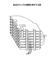
チップ積層に関する(特許文献1)には、半導体チップの積層の一形態が示されているが、ウエハのダイシング後の半導体チップの側面の外部接続に、複雑な製造工程を要していた。例えば、半導体チップを多段積層後、異方性導電膜又はフレキシブル回路基板を使用し又は絶縁膜と導電膜を成膜するなどの複雑な製造工程である。また、図1に示す他の半導体チップの積層の形態(特許文献2)においては、例えば、半導体チップのダイシング後、半導体チップ11の側面12の絶縁のための窒化物をスパッタリングする等の複雑な工程を要していた。このように、チップ積層の製造工程は、複雑であり、製品品質にも影響を与えていた。
The chip stacking (Patent Document 1) shows one form of stacking of semiconductor chips, but a complicated manufacturing process is required for external connection of the side surfaces of the semiconductor chips after wafer dicing. For example, it is a complicated manufacturing process such as using an anisotropic conductive film or a flexible circuit board or forming an insulating film and a conductive film after stacking semiconductor chips in multiple stages. Further, in the stacked form of other semiconductor chips shown in FIG. 1 (Patent Document 2), for example, after dicing the semiconductor chip, a complicated process such as sputtering nitride for insulating the
本発明は、このような問題点を解決するためになされたものであって、工程の簡略化と製品品質の向上を目的とする。 The present invention has been made to solve such problems, and aims to simplify the process and improve the product quality.
上記目的を達成するため、本発明に係る半導体チップ積層体は、接続端子を有する配線基板と、前記配線基板上に積層された、パッドを有する複数の半導体チップと、一方の端部が前記複数の半導体チップの前記パッドと接続され、他方の端部が前記複数の半導体チップの側面から突出する導電性連結材と、前記複数の半導体チップにおける前記導電性連結材の前記他方の端部と前記配線基板の前記接続端子とを接続する導電性部材と、を有し、前記複数の半導体チップの側面には前記複数の半導体チップの各々を構成する導電性材料が露出しており、前記複数の半導体チップの側面と前記導電性部材との間には間隙が設けられ、前記導電性部材は、導電性ペースト、又は、はんだの何れか一の材料であり、前記複数の半導体チップ、前記導電性連結材、前記導電性部材、及び前記間隙は、同一の封止樹脂により覆われていることを要件とする。
In order to achieve the above object, a semiconductor chip laminated body according to the present invention includes a wiring board having connection terminals, a plurality of semiconductor chips having pads stacked on the wiring board, and one end portion of the plurality of semiconductor chips. A conductive connecting member connected to the pad of the semiconductor chip and having the other end protruding from a side surface of the plurality of semiconductor chips; the other end of the conductive connecting member in the plurality of semiconductor chips; A conductive member that connects the connection terminals of the wiring board, and a conductive material constituting each of the plurality of semiconductor chips is exposed on a side surface of the plurality of semiconductor chips , gap provided we are between the side surface of the semiconductor chip and the conductive member, the conductive member is conductive paste, or a any one of the material of the solder, the plurality of semiconductor chips, the electrically Sex connecting member, the conductive member, and the gap, it is a requirement that is covered by the same sealing resin.
本発明により、工程の簡略化と製品品質の向上の目的を実現することができる。 According to the present invention, the object of simplification of the process and improvement of product quality can be realized.
以下、図面を参照して、本発明を実施するための最良の実施の形態を説明する。 The best mode for carrying out the present invention will be described below with reference to the drawings.
〈第1の実施の形態〉
図2は、本発明の第1の実施の形態に係る半導体チップ積層体を例示する断面図である。図2を参照するに、半導体チップ積層体20Aは、配線基板51と、配線基板51上に載置されたチップ積層体52Cとを有する。チップ積層体52Cは、パッド33を含む複数の半導体チップ32と、それぞれのパッド33に接続されたボンディングワイヤ34aと、導電性部材47と、封止樹脂48とを有する。
<First Embodiment>
FIG. 2 is a cross-sectional view illustrating a semiconductor chip stacked body according to the first embodiment of the invention. Referring to FIG. 2, the semiconductor chip stacked body 20 </ b> A includes a
チップ積層体52Cにおいて、複数の半導体チップ32は絶縁樹脂42を介して積層され、積層された複数の半導体チップ32は絶縁樹脂46を介して配線基板51上に載置されている。又、チップ積層体52Cにおいて、複数の半導体チップ32の側面から突出する各ボンディングワイヤ34aの端部は導電性部材47により配線基板51の接続端子61と導電接続され、その全体または一部が封止樹脂48により封止されている。
In the chip stacked body 52 </ b> C, the plurality of
半導体チップ32は、例えばシリコン等であるが、その側面は二酸化珪素等の絶縁膜により保護・絶縁されてなく、導電性材料(シリコン等)が露出している。一方、導電性部材47は、例えば、銀ペースト等の導電性ペーストや、はんだ等の導電性材料からなる。このように、近接して配置される各々の半導体チップ32の側面と導電性部材47とは共に導電性を有しているため、各々の半導体チップ32の側面と導電性部材47との接触を防止する必要がある。そのため、各々の半導体チップ32の側面と導電性部材47との間には間隙W1が設けられている。各々の半導体チップ32の側面と導電性部材47との接触を防止するためには、間隙W1は50μm以上とすることが好ましい。
The
このように、半導体チップ積層体において、各々の半導体チップの側面と導電性部材との間に所定の間隔を設けるようにする。その結果、後述する半導体チップ積層体の製造方法において、各々の半導体チップの側面に絶縁膜を形成する工程が不要となり、半導体チップ積層体の形成工程を簡素化して、生産性の向上を図ることができる。 As described above, in the semiconductor chip stacked body, a predetermined interval is provided between the side surface of each semiconductor chip and the conductive member. As a result, in the method of manufacturing a semiconductor chip laminate described later, a process of forming an insulating film on the side surface of each semiconductor chip is not required, and the process of forming the semiconductor chip laminate is simplified to improve productivity. Can do.
図3は、本発明の第1の実施の形態に係る半導体チップ積層体の製造方法のステップを例示する図である。製造方法のステップは、(S100.準備)、(S101.連結材接続)、(S102.チップ積層)、(S103.積層体・基板接続)及び(S104.樹脂封止)の各ステップを有している。以下各ステップについて、対応する図を参照しながら、説明する。 FIG. 3 is a diagram illustrating steps in the method for manufacturing a semiconductor chip stacked body according to the first embodiment of the invention. The steps of the manufacturing method include the steps of (S100. Preparation), (S101. Connection material connection), (S102. Chip stacking), (S103. Stacked body / substrate connection) and (S104. Resin sealing). ing. Hereinafter, each step will be described with reference to the corresponding drawings.
(S100.準備工程)
例えば、外径が6インチ、8インチまたは12インチの半導体ウエハを準備し、バックグラインド等による薄型化を施し、さらに個々の半導体チップにダイシング(個片化)する。ダイシングを終えた半導体チップは、ダイシングテープ上に置かれている。
(S100. Preparation step)
For example, a semiconductor wafer having an outer diameter of 6 inches, 8 inches, or 12 inches is prepared, thinned by back grinding or the like, and further diced into individual semiconductor chips. The semiconductor chip that has been diced is placed on a dicing tape.
(S101.連結材接続)
工程a.において、S100で準備した個々の半導体チップを、ダイシングテープからピックアップして、仮接着フィルム上に載置する。仮接着フィルムの材質としては、例えば、ポリエステルフィルムを使用することができる。
(S101. Connection material connection)
Step a. The individual semiconductor chips prepared in S100 are picked up from the dicing tape and placed on the temporary adhesive film. As a material of the temporary adhesive film, for example, a polyester film can be used.
工程b.において、半導体チップ上のパッドに、導電性連結材を接続する。導電性連結材としては、例えば、ボンディングワイヤを使用する。以下、導電性連結材としてボンディングワイヤを用いる場合を例に説明する。 Step b. The conductive coupling material is connected to the pads on the semiconductor chip. For example, a bonding wire is used as the conductive connecting material. Hereinafter, a case where a bonding wire is used as the conductive connecting material will be described as an example.
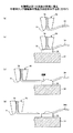
図4は、連結材接続工程において使用するワイヤボンダ装置のボンディングツール70の先端部を例示する図である。図4の(a)は、ボンディングツール70の斜視図であり、(b)は矢視Zの向きから見た底面図であり、(c)は矢視X−Xの側面図であり、(d)は矢視Y−Yの側面図である。(b)における中央の孔部74は、ボンディングワイヤを通過させるための貫通孔であり、ボンディングツール70がキャピラリの機能を有している。また、ボンディングツール70は、底面部71と、溝72,73とを有している。溝72,73の深さh1,h2及び開口部の開口角度θ1,θ2は異なっており、用途により溝72及び溝73を適宜使い分けることができる。
FIG. 4 is a diagram illustrating the tip of the
図5は、ボンディングワイヤ34aを、仮接着フィルム31上に載置された半導体チップ32のパッド33に接続した状態を示す図である。図5において、41aは半導体チップ32の集積回路面を、41bは半導体チップ32の背面を示している。
FIG. 5 is a view showing a state in which the
なお、各ボンディングワイヤ34aの長さの設定については、配線基板上における熱圧着時等に変形するボンディングワイヤの変形量も、予め考慮する。ボンディングワイヤ34aの材質としては、金、銅、アルミニウム、タングステン、又はそれらの合金等を使用することができ、その直径としては、通常、15μm〜30μmである。また、半導体チップ32の厚さは、例えば、40〜50μmであるが、半導体の機能、製品の用途等に応じて様々な値を有する。
In addition, regarding the setting of the length of each
ここで、各々の半導体チップ32の角部に斜面等の切欠きを設けて、エッジ部付近の空間を広く保つことにより、ボンディングワイヤ34aの各々の半導体チップ32のエッジ部等への接触を避けることも可能である。斜面等の切欠きの方法としては、例えば、半導体チップを個片化する際に、ダイサ装置を用いたベベルカットを行う等の方法を使用することができる。
Here, a notch such as a slope is provided at the corner of each
図6は、図4に示したボンディングツール70を用いて、図5に示した半導体チップ32のパッド33にボンディングワイヤ34aを接続する方法を例示する図である。始めに、図6の(a)に示すように、ボンディングツール70の孔部74から、予めボンディングワイヤ34を所定の長さだけ送り出し、所定の形状に整形しておく。なお、ボンディングワイヤ34は、最終的に切断されてボンディングワイヤ34aとなる。
FIG. 6 is a diagram illustrating a method of connecting the
次いで、図6の(b)に示すように、ボンディングツール70の底面部71を半導体チップ32のパッド33に当接し、ボンディングワイヤ34に超音波振動を付与するとともに加熱及び加圧して、ボンディングワイヤ34をパッド33に接続する。
Next, as shown in FIG. 6B, the
次いで、図6の(c)に示すように、ボンディングワイヤ34を所定の長さだけ送り出しながらボンディングツール70を移動させる。このとき、図6の(c)の矢印部のボンディングワイヤ34は細くなっているため、図6の(d)に示すように、図6の(c)の矢印部で容易に切断することができる。このようにして、図5に示した半導体チップ32のパッド33にボンディングワイヤ34aを接続することができる。
Next, as shown in FIG. 6C, the
なお、図7に示すように、半導体チップ32の間隙35を跨ぐ形状をもって、パッド33同士を導電性連結材36で連結する。そして、導電性連結材36を切断箇所37において切断することにより、図5に示した半導体チップ32のパッド33にボンディングワイヤ34aを接続しても構わない(導電性連結材36を切断したものをボンディングワイヤ34aとする)。
As shown in FIG. 7, the
(S102.チップ積層 a.絶縁樹脂塗布)
個々の半導体チップ32を前出の図5又は図7で示した仮接着フィルム31上から剥離し、ボンディングワイヤ34aを有する半導体チップ32の背面41bに絶縁樹脂42を塗布する。絶縁樹脂42の塗布は、周知のスクリーン印刷法、スピンコート法またはフィルム状シートの貼り付け等により行うことができる。
(S102. Chip lamination a. Application of insulating resin)
Each
絶縁樹脂42の材質としては、例えば、エポキシ系樹脂等を使用する。また、熱可塑性の機能を有するものを使用することができる。次の工程(b.チップ積層)に備えて、絶縁樹脂を仮硬化させる。仮硬化の温度としては、例えば、スクリーン印刷法の場合125℃、スピンコート法の場合125℃、フィルム状シート使用の場合80℃である。
As a material of the insulating
(S102.チップ積層 b.チップ積層)
図8は、ボンディングワイヤ34a及び絶縁樹脂42を有する半導体チップ32が、配線基板51上に載置され、全体としてチップ積層体52Aが形成された状態を示している。個々の半導体チップをピックアップして、チップ積層を行うが、チップ積層体52Aの形成のためには、ダイマウント装置またはフリップチップマウンタ装置を使用し、半導体チップのアライメントと固定を行う。チップ積層体の配線基板への搭載における絶縁樹脂による固定は、例えば、150℃の温度で30分の温度条件により行う。
(S102. Chip lamination b. Chip lamination)
FIG. 8 shows a state in which the
ただし、最上層の半導体チップ32の集積回路面41a上の絶縁樹脂は不要である。一方、最下層の半導体チップ32の背面41bの配線基板への載置部分には、接着用の絶縁樹脂46を設ける。絶縁樹脂46の材質としては、ダイボンディングペーストを使用することができる。ダイボンディングペーストの材料としては、例えばアルミナをフィラーに含むエポキシ系のペーストを使用することができる。
However, the insulating resin on the
最下層の半導体チップ32の配線基板51との対向面における絶縁樹脂46の箇所においては、半導体チップが上向きのため、連結材(ボンディングワイヤ)が存在しない。従って、絶縁樹脂46のスペーサとしての機能が不要であり、絶縁樹脂46の厚さを薄くすることができる。半導体チップが下向きの場合と比較すると、チップ積層体52Aの全体の厚さを減少させることができる。なお、半導体チップ32の側面は、二酸化珪素等の絶縁膜により保護・絶縁されてなく、導電性材料(シリコン等)が露出している。
At the location of the insulating
(S103.積層体・基板接続)
図9は、半導体チップ32の有するボンディングワイヤ34aの端部が、導電性部材47により配線基板51上の接続端子61と導電接続され、全体としてチップ積層体52Bが形成された状態を示している。前出の図8において積層された半導体チップ32の側面から突出する各ボンディングワイヤ34aの端部は、導電性部材47により配線基板51の接続端子61と導電接続されている。導電性部材47としては、例えば、高粘度でチクソ性を有する銀ペーストやはんだ等を使用することができる。
(S103. Laminate / Board connection)
FIG. 9 shows a state in which the end portion of the
半導体チップ32の側面から突出する各ボンディングワイヤ34aの端部の、導電性部材47による配線基板51の接続端子61との導電接続は、例えば以下のようにする。すなわち、始めに、導電性部材47を供給するシリンジ49を準備し、シリンジ49を配線基板51の接続端子61近傍に移動する。次いで、シリンジ49から接続端子61に導電性部材47を供給しながら、シリンジ49の位置を図9の矢印方向に移動させる。
Conductive connection of the end of each
この際、半導体チップ32の側面は、二酸化珪素等の絶縁膜により保護・絶縁されてなく、導電性材料(シリコン等)が露出しているため、導電性部材47が半導体チップ32の側面と接触する虞がある。そこで、半導体チップ32の側面と導電性部材47とは、間隙W1を空けなければならない。半導体チップ32の側面と導電性部材47との接触を防止するためには、間隙W1は50μm以上とすることが好ましい。
At this time, the side surface of the
導電性部材47として高粘度でチクソ性を有する材料を使用することにより、導電性部材47が半導体チップ32と接触しない状態で(間隙W1を空けた状態で)、半導体チップ32の側面から突出する各ボンディングワイヤ34aの端部を、導電性部材47により配線基板51の接続端子61と導電接続することができる。なお、導電性部材47の粘度は10000CP以上であることが好ましく、チクソ性は4.0以上であることが好ましい。導電性部材47の粘度及びチクソ性をこのような範囲とすることにより、導電性部材47を垂直(Z方向)に形成する際の液だれを防止することができる。
By using a material having high viscosity and thixotropy as the
(S104.樹脂封止)
図9に示す積層体・基板接続工程の後に、チップ積層体、接続端子と接続された導電性連結材及び配線基板について、その全体または一部を封止樹脂48により封止することにより、図2に示す半導体チップ積層体20Aが完成する。
(S104. Resin sealing)
After the laminated body / substrate connecting step shown in FIG. 9, the chip laminated body, the conductive connecting material connected to the connection terminals, and the wiring board are sealed in whole or part with a sealing
樹脂封止の方法は、トンラスファーモールド法またはポッティング法等を使用する。図2の例では、半導体チップからの放熱等のために、最上層のチップの集積回路面を封止樹脂48から露出させているが、半導体製品の使用条件に応じて、全面を封止することも可能であり、種々の封止の形態をとることができる。
As a resin sealing method, a ton-laser mold method or a potting method is used. In the example of FIG. 2, the integrated circuit surface of the uppermost chip is exposed from the sealing
また、半導体チップと配線基板との熱膨張差に起因する内部応力がパッドの箇所等に発生しうるような場合であっても、ボンディングワイヤの弾性によって熱膨張差を吸収することができる。そのため、封止樹脂によってボンディングワイヤの自由な動きが妨げられることがないように、封止箇所を限定して、樹脂封止を行うことができる。 Further, even when an internal stress due to a difference in thermal expansion between the semiconductor chip and the wiring substrate can be generated at a pad portion or the like, the difference in thermal expansion can be absorbed by the elasticity of the bonding wire. Therefore, resin sealing can be performed by limiting the sealing locations so that the free movement of the bonding wire is not hindered by the sealing resin.
〈第1の実施の形態の効果〉
各々の半導体チップに接続されたボンディングワイヤを、導電性部材により配線基板の接続端子と導電接続する際に、各々の半導体チップの側面と導電性部材との間に所定の間隔を空けるようにする。その結果、各々の半導体チップの側面に絶縁膜を形成する工程が不要となり、半導体チップ積層体の形成工程を簡素化して、生産性の向上を図ることができる。
<Effect of the first embodiment>
When a bonding wire connected to each semiconductor chip is conductively connected to the connection terminal of the wiring board by the conductive member, a predetermined gap is provided between the side surface of each semiconductor chip and the conductive member. . As a result, a process for forming an insulating film on the side surface of each semiconductor chip is not required, and the process for forming a semiconductor chip stacked body can be simplified to improve productivity.
又、配線基板上の接続端子に向けて、各々の半導体チップに接続されたボンディングワイヤを個別に引き回すことが不要であり、半導体チップに接続されたボンディングワイヤの長さを短縮することができる。従って、従来の積層型半導体装置と比較して、本発明の半導体チップ積層体の、パッケージのインダクタンス(L)についての電気的特性が大幅に向上する。 Further, it is not necessary to individually route the bonding wires connected to each semiconductor chip toward the connection terminals on the wiring board, and the length of the bonding wires connected to the semiconductor chip can be shortened. Therefore, as compared with the conventional stacked semiconductor device, the electrical characteristics of the package of the semiconductor chip of the present invention with respect to the package inductance (L) are greatly improved.
更に、各々の半導体チップの集積回路面が上向き(Z+側向き)になるように積層しているため、チップ積層体の最下層の半導体チップと配線基板との間隙を狭めることができる。従って、チップ積層体の全体の厚さをさらに薄くして、コンパクトな半導体チップ積層体を提供することができる。 Further, since the integrated circuit surfaces of the respective semiconductor chips are stacked so as to face upward (Z + side direction), the gap between the lowermost semiconductor chip of the chip stack and the wiring board can be narrowed. Therefore, the entire thickness of the chip stack can be further reduced to provide a compact semiconductor chip stack.
〈第2の実施の形態〉
図10は、本発明の第2の実施の形態に係る半導体チップ積層体を例示する断面図である。同図中、図2と同一の構成部分については同一符号を付し、その説明を省略する場合がある。
<Second Embodiment>
FIG. 10 is a cross-sectional view illustrating a semiconductor chip stacked body according to the second embodiment of the invention. In the figure, the same components as those in FIG. 2 are denoted by the same reference numerals, and the description thereof may be omitted.
図10を参照するに、半導体チップ積層体20Bは、搭載する半導体チップ32が半導体チップ32Aに置換された点を除いて図2に示す半導体チップ積層体20Aと同一の構造である。以下、半導体チップ積層体20Bについて、半導体チップ積層体20Aと同一の部分についてはその説明を省略し、半導体チップ積層体20Aと異なる部分を中心に説明する。
Referring to FIG. 10, the semiconductor chip stacked body 20B has the same structure as the semiconductor chip stacked
チップ積層体52Dにおいて、ボンディングワイヤ34aは、左右対称ではなく、任意の方向にのみ突出している。突出する方向は任意で構わないが、図10の例では、ある半導体チップ32Aにおいてボンディングワイヤ34aの一端がX+方向に突出していれば、隣接する半導体チップ32Aにおいてボンディングワイヤ34aの一端がX−方向に突出している。
In the chip stacked
このように、半導体チップ積層体において、ボンディングワイヤは左右対称ではなく、任意の方向にのみ突出していても構わない。 As described above, in the semiconductor chip stacked body, the bonding wires are not symmetrical and may protrude only in an arbitrary direction.
半導体チップ積層体20Bは、図2「本発明の第1の実施の形態に係る半導体チップ積層体の製造方法のステップを例示する図」と同様の工程で製造できるため、その製造方法の説明は省く。 The semiconductor chip stacked body 20B can be manufactured in the same process as FIG. 2 “the figure illustrating the steps of the method of manufacturing the semiconductor chip stacked body according to the first embodiment of the present invention”. Omit.
〈第2の実施の形態の効果〉
第1の実施の形態と同様の効果を奏するが、更に以下の効果を奏する。すなわち、半導体チップ積層体に搭載できる半導体チップの種類を増やすことができる。
<Effects of Second Embodiment>
Although the same effect as the first embodiment is obtained, the following effect is further obtained. That is, the types of semiconductor chips that can be mounted on the semiconductor chip stack can be increased.
〈第3の実施の形態〉
図11は、本発明の第3の実施の形態に係る半導体チップ積層体を例示する断面図である。同図中、図2と同一の構成部分については同一符号を付し、その説明を省略する場合がある。
<Third Embodiment>
FIG. 11 is a cross-sectional view illustrating a semiconductor chip stacked body according to the third embodiment of the invention. In the figure, the same components as those in FIG. 2 are denoted by the same reference numerals, and the description thereof may be omitted.
図11を参照するに、半導体チップ積層体20Cは、チップ積層体52Eにおいて、搭載する半導体チップ32が半導体チップ32、32B、及び32Cに置換された点を除いて図2に示す半導体チップ積層体20Aと同一の構造である。以下、半導体チップ積層体20Cについて、半導体チップ積層体20Aと同一の部分についてはその説明を省略し、半導体チップ積層体20Aと異なる部分を中心に説明する。
Referring to FIG. 11, the semiconductor chip stacked body 20C is the same as the semiconductor chip stacked body shown in FIG. 2 except that the
半導体チップ32と、半導体チップ32Bと、半導体チップ32Cとは、それぞれチップサイズが異なる。又、半導体チップ32B及び32Cのパッド33に接続されているボンディングワイヤ34b及び34cは、半導体チップ32のパッド33に接続されているボンディングワイヤ34aよりも長くなっている。それぞれのボンディングワイヤの一端を導電性部材47で導電接続するためである。
The
このように、半導体チップ積層体において、チップサイズが異なる半導体チップを積層しても構わない。又、半導体チップ積層体において、必要に応じて、ボンディングワイヤの長さを変えても構わない。 As described above, semiconductor chips having different chip sizes may be stacked in the semiconductor chip stacked body. Further, in the semiconductor chip laminated body, the length of the bonding wire may be changed as necessary.
半導体チップ積層体20Cは、図2「本発明の第1の実施の形態に係る半導体チップ積層体の製造方法のステップを例示する図」と同様の工程で製造できるため、その製造方法の説明は省く。 The semiconductor chip stacked body 20C can be manufactured in the same process as FIG. 2 “the figure illustrating the steps of the method for manufacturing the semiconductor chip stacked body according to the first embodiment of the present invention”. Omit.
〈第3の実施の形態の効果〉
第1の実施の形態と同様の効果を奏するが、更に以下の効果を奏する。すなわち、半導体チップ積層体において、ボンディングワイヤの長さを調整することにより、チップサイズが異なる半導体チップを積層することができる。
<Effect of the third embodiment>
Although the same effect as the first embodiment is obtained, the following effect is further obtained. That is, semiconductor chips having different chip sizes can be stacked by adjusting the length of the bonding wire in the semiconductor chip stacked body.
〈第4の実施の形態〉
図12は、本発明の第4の実施の形態に係る半導体チップ積層体を例示する断面図である。同図中、図2と同一の構成部分については同一符号を付し、その説明を省略する場合がある。
<Fourth embodiment>
FIG. 12 is a cross-sectional view illustrating a semiconductor chip stacked body according to the fourth embodiment of the invention. In the figure, the same components as those in FIG. 2 are denoted by the same reference numerals, and the description thereof may be omitted.
図12を参照するに、半導体チップ積層体20Dは、チップ積層体52Fにおいて、半導体チップ32が集積回路面を配線基板51側(Z−側)に向けて積層されている点を除いて図2に示す半導体チップ積層体20Aと同一の構造である。
Referring to FIG. 12, the semiconductor chip stacked
このように、半導体チップ積層体において、各々の半導体チップの集積回路面が下向き(Z−側向き)になるように積層しても構わない。 In this manner, in the semiconductor chip stacked body, stacking may be performed so that the integrated circuit surface of each semiconductor chip faces downward (toward the Z-side).
半導体チップ積層体20Dは、図2「本発明の第1の実施の形態に係る半導体チップ積層体の製造方法のステップを例示する図」と同様の工程で製造できるため、その製造方法の説明は省く。
The semiconductor chip stacked
〈第4の実施の形態の効果〉
第1の実施の形態と同様の効果を奏するが、更に以下の効果を奏する。すなわち、図4又は図6に示す工程と同一工程において、各々の半導体チップの集積回路面側に絶縁樹脂を塗布することができるため、半導体チップ積層体の形成工程を簡素化して、生産性の向上を図ることができる。
<Effect of the fourth embodiment>
Although the same effect as the first embodiment is obtained, the following effect is further obtained. That is, since the insulating resin can be applied to the integrated circuit surface side of each semiconductor chip in the same process as the process shown in FIG. 4 or FIG. 6, the process of forming the semiconductor chip stack is simplified, and the productivity is improved. Improvements can be made.
〈第5の実施の形態〉
図13は、本発明の第5の実施の形態に係る半導体チップ積層体を例示する断面図である。同図中、図2と同一の構成部分については同一符号を付し、その説明を省略する場合がある。
<Fifth embodiment>
FIG. 13 is a cross-sectional view illustrating a semiconductor chip stacked body according to the fifth embodiment of the invention. In the figure, the same components as those in FIG. 2 are denoted by the same reference numerals, and the description thereof may be omitted.
図13を参照するに、半導体チップ積層体20Eは、チップ積層体52Gにおいて、最下層の半導体チップ32Dが配線基板51にフリップチップ接続されている点を除いて図2に示す半導体チップ積層体20Aと同一の構造である。以下、半導体チップ積層体20Eについて、半導体チップ積層体20Aと同一の部分についてはその説明を省略し、半導体チップ積層体20Aと異なる部分を中心に説明する。
Referring to FIG. 13, the semiconductor chip stacked
図13において、バンプ82は、最下層の半導体チップ32Dの集積回路面のパッド81上に形成され、バンプ82の端面は、集積回路面上に塗布された絶縁樹脂84の表面に露出している。
In FIG. 13, bumps 82 are formed on the
バンプ82の形成の方法としては、ボンディングワイヤを用いたボールボンディング、または単独に形成したボールを載置固定するボールバンプ方法等を用いる。フリップチップ接続により、半導体チップ32Dのバンプ82を、配線基板51上の接続端子83と接続する。接続端子83上には、スズ、銀等の成分のはんだを塗布してフリップチップ接続を行うことができる。
As a method for forming the
このように、半導体チップ積層体において、最下層の半導体チップを配線基板にフリップチップ接続しても構わない。 Thus, in the semiconductor chip stack, the lowermost semiconductor chip may be flip-chip connected to the wiring board.
半導体チップ積層体20Eは、フリップチップ接続以外の工程は図2「本発明の第1の実施の形態に係る半導体チップ積層体の製造方法のステップを例示する図」と同様の工程で製造できるため、その製造方法の説明は省く。
The semiconductor chip stacked
〈第5の実施の形態の効果〉
第1の実施の形態と同様の効果を奏するが、更に以下の効果を奏する。すなわち、例えば、KGD(Known Good Die)としてのメモリとロジックの複合した半導体チップの積層体等を構成することができるので、半導体パッケージの設計において、半導体チップ積層体の形態を利用できる半導体チップの範囲を拡大することができる。そして、半導体チップの積層体をコンパクトな形態にすることができるので、さらに性能の向上を図ることができる。
<Effect of Fifth Embodiment>
Although the same effect as the first embodiment is obtained, the following effect is further obtained. That is, for example, a stacked body of a semiconductor chip in which a memory and logic as KGD (Known Good Die) are combined can be configured. Therefore, in the design of a semiconductor package, a semiconductor chip that can use the form of the semiconductor chip stacked body The range can be expanded. And since the laminated body of a semiconductor chip can be made into a compact form, a performance improvement can be aimed at further.
〈本発明に係る他の実施の形態〉
以上、本発明の好ましい実施の形態について詳説したが、本発明は、上述した実施の形態に制限されることはなく、本発明の範囲を逸脱することなく、上述した実施の形態に種々の変形及び置換を加えることができる。
<Other Embodiments According to the Present Invention>
The preferred embodiment of the present invention has been described in detail above. However, the present invention is not limited to the above-described embodiment, and various modifications can be made to the above-described embodiment without departing from the scope of the present invention. And substitutions can be added.
20A、20B、20D、20E 半導体チップ積層体
31 仮接着フィルム
32、32A、32B、32C、32D 半導体チップ
33 パッド
34、34a、34b、34c ボンディングワイヤ
35 間隙
36 導電性連結材
37 切断箇所
41a 集積回路面
41b 背面
42、46 絶縁樹脂
47 導電性部材
48 封止樹脂
49 シリンジ
51 配線基板
52A、52B、52C、52D、52E、52F、52G チップ積層体
61 接続端子
70 ボンディングツール
71 底面部
72、73 溝
74 孔部
81 パッド
82 バンプ
83 接続端子
84 絶縁樹脂
h1、h2 深さ
θ1,θ2 開口角度
W1 間隔
20A, 20B, 20D, 20E Semiconductor chip laminated
Claims (5)
前記配線基板上に積層された、パッドを有する複数の半導体チップと、
一方の端部が前記複数の半導体チップの前記パッドと接続され、他方の端部が前記複数の半導体チップの側面から突出する導電性連結材と、
前記複数の半導体チップにおける前記導電性連結材の前記他方の端部と前記配線基板の前記接続端子とを接続する導電性部材と、を有し、
前記複数の半導体チップの側面には前記複数の半導体チップの各々を構成する導電性材料が露出しており、前記複数の半導体チップの側面と前記導電性部材との間には間隙が設けられ、
前記導電性部材は、導電性ペースト、又は、はんだの何れか一の材料であり、
前記複数の半導体チップ、前記導電性連結材、前記導電性部材、及び前記間隙は、同一の封止樹脂により覆われている半導体チップ積層体。 A wiring board having connection terminals;
A plurality of semiconductor chips having pads, stacked on the wiring substrate;
One end portion is connected to the pads of the plurality of semiconductor chips, and the other end portion protrudes from a side surface of the plurality of semiconductor chips;
A conductive member that connects the other end of the conductive connecting member in the plurality of semiconductor chips and the connection terminal of the wiring board;
Wherein the side surface of the plurality of semiconductor chips are exposed conductive material constituting each of the plurality of semiconductor chips, gaps provided et Re between the side surface and the conductive member of the plurality of semiconductor chips ,
The conductive member is a conductive paste or any one material of solder,
The semiconductor chip stack in which the plurality of semiconductor chips, the conductive connecting material, the conductive member, and the gap are covered with the same sealing resin .
Priority Applications (2)
| Application Number | Priority Date | Filing Date | Title |
|---|---|---|---|
| JP2009145430A JP5215244B2 (en) | 2009-06-18 | 2009-06-18 | Semiconductor device |
| US12/768,938 US8058717B2 (en) | 2009-06-18 | 2010-04-28 | Laminated body of semiconductor chips including pads mutually connected to conductive member |
Applications Claiming Priority (1)
| Application Number | Priority Date | Filing Date | Title |
|---|---|---|---|
| JP2009145430A JP5215244B2 (en) | 2009-06-18 | 2009-06-18 | Semiconductor device |
Publications (3)
| Publication Number | Publication Date |
|---|---|
| JP2011003715A JP2011003715A (en) | 2011-01-06 |
| JP2011003715A5 JP2011003715A5 (en) | 2012-06-07 |
| JP5215244B2 true JP5215244B2 (en) | 2013-06-19 |
Family
ID=43353539
Family Applications (1)
| Application Number | Title | Priority Date | Filing Date |
|---|---|---|---|
| JP2009145430A Expired - Fee Related JP5215244B2 (en) | 2009-06-18 | 2009-06-18 | Semiconductor device |
Country Status (2)
| Country | Link |
|---|---|
| US (1) | US8058717B2 (en) |
| JP (1) | JP5215244B2 (en) |
Families Citing this family (15)
| Publication number | Priority date | Publication date | Assignee | Title |
|---|---|---|---|---|
| US8680686B2 (en) * | 2010-06-29 | 2014-03-25 | Spansion Llc | Method and system for thin multi chip stack package with film on wire and copper wire |
| US9530753B2 (en) * | 2011-09-23 | 2016-12-27 | STATS ChipPAC Pte. Ltd. | Integrated circuit packaging system with chip stacking and method of manufacture thereof |
| US9093457B2 (en) | 2012-08-22 | 2015-07-28 | Freescale Semiconductor Inc. | Stacked microelectronic packages having patterned sidewall conductors and methods for the fabrication thereof |
| US9064977B2 (en) | 2012-08-22 | 2015-06-23 | Freescale Semiconductor Inc. | Stacked microelectronic packages having sidewall conductors and methods for the fabrication thereof |
| US9190390B2 (en) | 2012-08-22 | 2015-11-17 | Freescale Semiconductor Inc. | Stacked microelectronic packages having sidewall conductors and methods for the fabrication thereof |
| US8860202B2 (en) * | 2012-08-29 | 2014-10-14 | Macronix International Co., Ltd. | Chip stack structure and manufacturing method thereof |
| US9299670B2 (en) | 2013-03-14 | 2016-03-29 | Freescale Semiconductor, Inc. | Stacked microelectronic packages having sidewall conductors and methods for the fabrication thereof |
| US9524950B2 (en) | 2013-05-31 | 2016-12-20 | Freescale Semiconductor, Inc. | Stacked microelectronic packages having sidewall conductors and methods for the fabrication thereof |
| KR102099878B1 (en) * | 2013-07-11 | 2020-04-10 | 삼성전자 주식회사 | Semiconductor Package |
| US9025340B2 (en) | 2013-09-30 | 2015-05-05 | Freescale Semiconductor, Inc. | Devices and stacked microelectronic packages with in-trench package surface conductors and methods of their fabrication |
| US9036363B2 (en) | 2013-09-30 | 2015-05-19 | Freescale Semiconductor, Inc. | Devices and stacked microelectronic packages with parallel conductors and intra-conductor isolator structures and methods of their fabrication |
| US9263420B2 (en) | 2013-12-05 | 2016-02-16 | Freescale Semiconductor, Inc. | Devices and stacked microelectronic packages with package surface conductors and methods of their fabrication |
| US9305911B2 (en) | 2013-12-05 | 2016-04-05 | Freescale Semiconductor, Inc. | Devices and stacked microelectronic packages with package surface conductors and adjacent trenches and methods of their fabrication |
| US10388607B2 (en) | 2014-12-17 | 2019-08-20 | Nxp Usa, Inc. | Microelectronic devices with multi-layer package surface conductors and methods of their fabrication |
| US11031341B2 (en) * | 2017-03-29 | 2021-06-08 | Intel Corporation | Side mounted interconnect bridges |
Family Cites Families (23)
| Publication number | Priority date | Publication date | Assignee | Title |
|---|---|---|---|---|
| US5675180A (en) | 1994-06-23 | 1997-10-07 | Cubic Memory, Inc. | Vertical interconnect process for silicon segments |
| JP3476383B2 (en) * | 1999-05-27 | 2003-12-10 | シャープ株式会社 | Semiconductor laminated package |
| JP3681155B2 (en) * | 1999-12-22 | 2005-08-10 | 新光電気工業株式会社 | Electronic component mounting structure, electronic component device, electronic component mounting method, and electronic component device manufacturing method |
| JP3708399B2 (en) * | 2000-03-13 | 2005-10-19 | 株式会社東芝 | Semiconductor device and manufacturing method thereof |
| JP4361670B2 (en) * | 2000-08-02 | 2009-11-11 | 富士通マイクロエレクトロニクス株式会社 | Semiconductor element stack, semiconductor element stack manufacturing method, and semiconductor device |
| JP2002184937A (en) * | 2000-12-18 | 2002-06-28 | Shinko Electric Ind Co Ltd | Mounting structure of semiconductor device |
| US7215018B2 (en) * | 2004-04-13 | 2007-05-08 | Vertical Circuits, Inc. | Stacked die BGA or LGA component assembly |
| CN100539135C (en) * | 2004-09-08 | 2009-09-09 | 松下电器产业株式会社 | Three-dimensional circuit device, the e-machine that uses it and manufacture method thereof |
| JP4551321B2 (en) * | 2005-07-21 | 2010-09-29 | 新光電気工業株式会社 | Electronic component mounting structure and manufacturing method thereof |
| JP4566866B2 (en) * | 2005-09-07 | 2010-10-20 | 新光電気工業株式会社 | Semiconductor package, semiconductor package mounting structure, and semiconductor package manufacturing method |
| KR100794658B1 (en) * | 2006-07-07 | 2008-01-14 | 삼성전자주식회사 | Method of forming semiconductor chip, the semiconductor chip so formed and chip stack package having the same |
| KR100813625B1 (en) * | 2006-11-15 | 2008-03-14 | 삼성전자주식회사 | Semiconductor device package |
| SG146460A1 (en) * | 2007-03-12 | 2008-10-30 | Micron Technology Inc | Apparatus for packaging semiconductor devices, packaged semiconductor components, methods of manufacturing apparatus for packaging semiconductor devices, and methods of manufacturing semiconductor components |
| KR100914977B1 (en) * | 2007-06-18 | 2009-09-02 | 주식회사 하이닉스반도체 | Method for fabricating stack package |
| JP5110995B2 (en) * | 2007-07-20 | 2012-12-26 | 新光電気工業株式会社 | Multilayer semiconductor device and manufacturing method thereof |
| JP5049684B2 (en) * | 2007-07-20 | 2012-10-17 | 新光電気工業株式会社 | Multilayer semiconductor device and manufacturing method thereof |
| JP5110996B2 (en) * | 2007-07-20 | 2012-12-26 | 新光電気工業株式会社 | Manufacturing method of stacked semiconductor device |
| US7781877B2 (en) * | 2007-08-07 | 2010-08-24 | Micron Technology, Inc. | Packaged integrated circuit devices with through-body conductive vias, and methods of making same |
| JP2009071095A (en) * | 2007-09-14 | 2009-04-02 | Spansion Llc | Method of manufacturing semiconductor device |
| TWI355061B (en) * | 2007-12-06 | 2011-12-21 | Nanya Technology Corp | Stacked-type chip package structure and fabricatio |
| KR101472900B1 (en) * | 2007-12-06 | 2014-12-15 | 페어차일드코리아반도체 주식회사 | Molded leadless package and methods of fabricating the same |
| TW200931634A (en) * | 2008-01-10 | 2009-07-16 | Abounion Technology Corp | Multi-channel stacked semiconductor device and method for fabricating the same, and stacking substrate applied to the semiconductor device |
| JP5136449B2 (en) * | 2009-02-06 | 2013-02-06 | 富士通株式会社 | Manufacturing method of semiconductor device |
-
2009
- 2009-06-18 JP JP2009145430A patent/JP5215244B2/en not_active Expired - Fee Related
-
2010
- 2010-04-28 US US12/768,938 patent/US8058717B2/en not_active Expired - Fee Related
Also Published As
| Publication number | Publication date |
|---|---|
| JP2011003715A (en) | 2011-01-06 |
| US20100320584A1 (en) | 2010-12-23 |
| US8058717B2 (en) | 2011-11-15 |
Similar Documents
| Publication | Publication Date | Title |
|---|---|---|
| JP5215244B2 (en) | Semiconductor device | |
| US7485490B2 (en) | Method of forming a stacked semiconductor package | |
| JP5529371B2 (en) | Semiconductor device and manufacturing method thereof | |
| US8786102B2 (en) | Semiconductor device and method of manufacturing the same | |
| TWI277187B (en) | Semiconductor device and manufacturing method for the same | |
| US7332820B2 (en) | Stacked die in die BGA package | |
| US20040245652A1 (en) | Semiconductor device, electronic device, electronic appliance, and method of manufacturing a semiconductor device | |
| TWI330872B (en) | Semiconductor device | |
| US20080316696A1 (en) | Semiconductor memory device and semiconductor memory card using the same | |
| JP2005183923A (en) | Semiconductor device and its manufacturing method | |
| US20090261476A1 (en) | Semiconductor device and manufacturing method thereof | |
| US8860215B2 (en) | Semiconductor device and method of manufacturing the same | |
| CN112530880B (en) | Semiconductor device and method for manufacturing semiconductor device | |
| JP2003273317A (en) | Semiconductor device and its manufacturing method | |
| WO2007026392A1 (en) | Semiconductor device and method for manufacturing same | |
| JP2008166439A (en) | Semiconductor device and manufacturing method thereof | |
| JP2001223326A (en) | Semiconductor device | |
| WO2007052476A1 (en) | Electronic circuit device and method for manufacturing same | |
| US20230099787A1 (en) | Semiconductor package and method of fabricating the same | |
| JP4175138B2 (en) | Semiconductor device | |
| US8810047B2 (en) | Semiconductor device and method of manufacturing the same | |
| JP3476383B2 (en) | Semiconductor laminated package | |
| JP2007214238A (en) | Semiconductor device and its manufacturing method | |
| JP2011023709A (en) | Semiconductor device and method of manufacturing the same | |
| JP4620366B2 (en) | Semiconductor device, semiconductor element manufacturing method, and semiconductor device manufacturing method |
Legal Events
| Date | Code | Title | Description |
|---|---|---|---|
| A521 | Request for written amendment filed |
Free format text: JAPANESE INTERMEDIATE CODE: A523 Effective date: 20120411 |
|
| A621 | Written request for application examination |
Free format text: JAPANESE INTERMEDIATE CODE: A621 Effective date: 20120411 |
|
| TRDD | Decision of grant or rejection written | ||
| A01 | Written decision to grant a patent or to grant a registration (utility model) |
Free format text: JAPANESE INTERMEDIATE CODE: A01 Effective date: 20130219 |
|
| A977 | Report on retrieval |
Free format text: JAPANESE INTERMEDIATE CODE: A971007 Effective date: 20130221 |
|
| A61 | First payment of annual fees (during grant procedure) |
Free format text: JAPANESE INTERMEDIATE CODE: A61 Effective date: 20130228 |
|
| R150 | Certificate of patent or registration of utility model |
Ref document number: 5215244 Country of ref document: JP Free format text: JAPANESE INTERMEDIATE CODE: R150 Free format text: JAPANESE INTERMEDIATE CODE: R150 |
|
| FPAY | Renewal fee payment (event date is renewal date of database) |
Free format text: PAYMENT UNTIL: 20160308 Year of fee payment: 3 |
|
| LAPS | Cancellation because of no payment of annual fees |