JP5215087B2 - Electronic circuit - Google Patents
Electronic circuit Download PDFInfo
- Publication number
- JP5215087B2 JP5215087B2 JP2008221221A JP2008221221A JP5215087B2 JP 5215087 B2 JP5215087 B2 JP 5215087B2 JP 2008221221 A JP2008221221 A JP 2008221221A JP 2008221221 A JP2008221221 A JP 2008221221A JP 5215087 B2 JP5215087 B2 JP 5215087B2
- Authority
- JP
- Japan
- Prior art keywords
- circuit
- signal
- input
- averaging
- holding
- Prior art date
- Legal status (The legal status is an assumption and is not a legal conclusion. Google has not performed a legal analysis and makes no representation as to the accuracy of the status listed.)
- Active
Links
- 238000004891 communication Methods 0.000 claims description 98
- 238000012935 Averaging Methods 0.000 claims description 87
- 230000003287 optical effect Effects 0.000 description 26
- 238000010586 diagram Methods 0.000 description 22
- 230000007274 generation of a signal involved in cell-cell signaling Effects 0.000 description 16
- 239000003990 capacitor Substances 0.000 description 9
- 230000000052 comparative effect Effects 0.000 description 9
- 230000005540 biological transmission Effects 0.000 description 4
- 238000006243 chemical reaction Methods 0.000 description 1
- 230000000295 complement effect Effects 0.000 description 1
- 230000007423 decrease Effects 0.000 description 1
- 239000000835 fiber Substances 0.000 description 1
- 238000000034 method Methods 0.000 description 1
- 238000012986 modification Methods 0.000 description 1
- 230000004048 modification Effects 0.000 description 1
- 239000013307 optical fiber Substances 0.000 description 1
- 230000000087 stabilizing effect Effects 0.000 description 1
Images


Landscapes
- Amplifiers (AREA)
Description
本発明は、電子回路及に関し、特に、入力端子と参照信号端子とを有する差動増幅回路を備え、入力信号を平均化した信号を参照信号として生成する電子回路に関する。 The present invention relates to an electronic circuit and, more particularly, to an electronic circuit that includes a differential amplifier circuit having an input terminal and a reference signal terminal and generates an averaged signal as a reference signal.
近年、PON(Passive Optical Network)方式のFTTH(Fiber to the home)が普及している。このシステムでは、各家庭から送信されてくる様々な振幅の光信号を受信し電気信号として増幅することが求められる。 In recent years, FTTH (Fiber to the home) of the PON (Passive Optical Network) method has become widespread. This system is required to receive optical signals of various amplitudes transmitted from each home and amplify them as electrical signals.
例えば、特許文献1には、PON方式の光通信に用いられる受信回路が開示されている。このような受信回路においては、フォトダイオード(PD)等の受光素子が光信号を受信し電流を出力する。トランスインピーダンスアンプ(TIA)がPDの出力した電流信号を電圧信号に変換する。差動増幅回路がTIAの出力信号と、TIAの出力信号の平均値に関係した参照信号と、を差動増幅し、TIAの出力信号が参照信号より高ければハイレベル、低ければローレベルを出力する。ここで、例えばPON方式の光通信に用いられる受信回路では、通信相手との距離の違いにより、光信号の振幅が異なる。このため、通信相手ごとに入力信号の平均値に関係した信号を参照信号として生成し、これと入力信号とを比較しハイレベル、ローレベルを出力する。
従来の受信回路においては、参照信号が入力信号の平均値に到達するまでの安定期間を要するため、入力信号が入力されてから一定時間を通信準備期間(プリアンブル期間ともいう)とし、ダミーの信号を受信する。しかしながら、このように生成された参照信号は、その後の通信期間において、入力光信号のレベル変動があると、その影響を受けて、本来の値とは異なってしまう。 In the conventional receiving circuit, since a stable period is required until the reference signal reaches the average value of the input signal, a predetermined time after the input signal is input is defined as a communication preparation period (also referred to as a preamble period), and a dummy signal Receive. However, the reference signal generated in this way is different from the original value under the influence of the fluctuation of the level of the input optical signal in the subsequent communication period.
本発明は、上記課題に鑑みなされたものであり、入力信号の影響で参照信号が変動することを抑制することを目的とする。 The present invention has been made in view of the above problems, and an object thereof is to suppress a reference signal from fluctuating due to an influence of an input signal.
本発明は、入力信号が入力される入力端子と参照信号端子とを有する差動増幅回路と、前記入力信号を平均化し平均化信号を生成する平均化回路と、前記参照信号端子と前記平均化回路の出力との間に設けられ、前記平均化信号を保持し前記参照信号端子に出力する第1保持回路と、前記第1保持回路と前記平均化回路との間に設けられた第1スイッチと、前記記第1保持回路の出力、および前記平均化回路の出力と前記第1スイッチとの間の出力ノードのいずれかを選択的に前記参照信号端子に接続する第2スイッチと、前記出力ノードと前記第2スイッチとの間に接続され、前記平均化信号を保持し前記第2スイッチに出力する第2保持回路と、を備えることを特徴とする電子回路である。本発明によれば、第1スイッチが第1保持回路と平均化回路とを遮断することにより、入力信号の影響で参照信号が変動することを抑制することができる。 The present invention provides a differential amplifier circuit having an input terminal to which an input signal is input and a reference signal terminal, an averaging circuit that averages the input signal to generate an averaged signal, the reference signal terminal, and the averaged signal A first holding circuit provided between the first holding circuit and the averaging circuit; and a first switch provided between the first holding circuit and the averaging circuit. And a second switch for selectively connecting one of an output of the first holding circuit and an output node between the output of the averaging circuit and the first switch to the reference signal terminal, and the output An electronic circuit comprising: a second holding circuit connected between a node and the second switch, holding the averaged signal and outputting the averaged signal to the second switch . According to the present invention, since the first switch cuts off the first holding circuit and the averaging circuit, it is possible to suppress the reference signal from fluctuating due to the influence of the input signal.
上記構成において、前記第1スイッチは、前記入力信号を平均化するための通信準備期間において、前記第1保持回路と前記平均化回路とを接続し、前記通信準備期間の後は前記第1保持回路と前記平均化回路とを遮断する構成とすることができる。この構成によれば、通信準備期間においては、入力信号の平均化信号を参照信号とすることができ、通信準備期間後は、入力信号の影響で参照信号が変動することを抑制することができる。 In the above configuration, the first switch connects the first holding circuit and the averaging circuit in a communication preparation period for averaging the input signals, and after the communication preparation period, the first holding circuit The circuit and the averaging circuit can be cut off. According to this configuration, the average signal of the input signal can be used as the reference signal in the communication preparation period, and the reference signal can be prevented from changing due to the influence of the input signal after the communication preparation period. .
上記構成において、前記第1スイッチは、前記入力信号を平均化するための通信準備期間において、前記第1保持回路と前記平均化回路とを接続し、前記通信準備期間の後は前記第1保持回路と前記平均化回路とを遮断し、前記第2スイッチは、前記通信準備期間において前記出力ノードを選択し前記参照信号端子に接続し、前記通信準備期間の後は前記第1保持回路の出力を選択し前記参照信号端子に接続する構成とすることができる。この構成によれば、通信準備期間においては、入力信号の平均化信号を参照信号とすることができ、通信準備期間後は、入力信号の影響で参照信号が変動することを抑制することができる。 In the above configuration, the first switch connects the first holding circuit and the averaging circuit in a communication preparation period for averaging the input signals, and after the communication preparation period, the first holding circuit The circuit is disconnected from the averaging circuit, and the second switch selects the output node and connects to the reference signal terminal in the communication preparation period, and outputs the first holding circuit after the communication preparation period. Can be selected and connected to the reference signal terminal. According to this configuration, the average signal of the input signal can be used as the reference signal in the communication preparation period, and the reference signal can be prevented from changing due to the influence of the input signal after the communication preparation period. .
本発明は、入力信号が入力される入力端子と参照信号端子とを有する差動増幅回路と、前記入力信号を平均化し平均化信号を生成する平均化回路と、前記参照信号端子と前記平均化回路の出力との間に設けられ、前記平均化信号を保持し前記参照信号端子に出力する第1保持回路と、前記第1保持回路と前記平均化回路との間に設けられた第1スイッチと、を具備し、前記第1保持回路の出力は前記平均化回路に入力され、前記平均化回路を介した前記第1保持回路の出力が前記参照信号端子に出力されることを特徴とする電子回路である。 The present invention provides a differential amplifier circuit having an input terminal to which an input signal is input and a reference signal terminal, an averaging circuit that averages the input signal to generate an averaged signal, the reference signal terminal, and the averaged signal A first holding circuit provided between the first holding circuit and the averaging circuit; and a first switch provided between the first holding circuit and the averaging circuit. If, comprising a, the output of the first holding circuit is input to the averaging circuit, the output of the first holding circuit through the averaging circuit is characterized in that it is output to the reference signal terminal It is an electronic circuit .
上記構成において、前記平均化回路は、前記入力信号および前記第1保持回路の出力のいずれかを選択して平均化することにより前記平均化信号を生成する構成とすることができる。この構成によれば、平均化回路が第1保持回路の出力を選択することにより、入力信号の影響で参照信号が変動することを抑制することができる。 In the above configuration, the averaging circuit may generate the average signal by selecting and averaging either the input signal or the output of the first holding circuit. According to this configuration, when the averaging circuit selects the output of the first holding circuit, the reference signal can be prevented from fluctuating due to the influence of the input signal.
上記構成において、前記第1スイッチは、前記入力信号を平均化するための通信準備期間において、前記第1保持回路と前記平均化回路とを接続し、前記通信準備期間の後は前記第1保持回路と前記平均化回路とを遮断し、前記平均化回路は、前記通信準備期間において前記入力信号を選択し平均化することにより前記平均化信号を生成し、前記通信準備期間の後は前記第1保持回路の出力を選択することにより前記平均化信号を生成する構成とすることができる。この構成によれば、通信準備期間においては、平均化信号を参照信号とすることができ、通信準備期間後は、入力信号の影響で参照信号が変動することを抑制することができる。 In the above configuration, the first switch connects the first holding circuit and the averaging circuit in a communication preparation period for averaging the input signals, and after the communication preparation period, the first holding circuit And the averaging circuit generates the average signal by selecting and averaging the input signal in the communication preparation period, and after the communication preparation period, the averaging signal is generated. The average signal can be generated by selecting the output of one holding circuit. According to this configuration, the averaged signal can be used as the reference signal during the communication preparation period, and the reference signal can be prevented from fluctuating due to the influence of the input signal after the communication preparation period.
上記構成において、前記平均化回路の出力と前記第1スイッチとの間に前記平均化信号を保持し、前記通信準備期間の後はその出力が前記参照信号端子に接続され、前記通信準備期間においてはその出力が前記第1スイッチに接続される第2保持回路が設けられ、前記第1保持回路は前記第2保持回路で保持された前記平均化信号を保持する構成とすることができる。この構成によれば、第2保持回路により、参照信号を早期に安定化させることができる。 In the above configuration, the averaged signal is held between the output of the averaging circuit and the first switch, and the output is connected to the reference signal terminal after the communication preparation period, and in the communication preparation period A second holding circuit whose output is connected to the first switch is provided, and the first holding circuit holds the averaged signal held by the second holding circuit. According to this configuration, the reference signal can be stabilized early by the second holding circuit.
上記構成において、前記第1保持回路は、前記入力信号のピークを保持するピークホールド回路またはローパスフィルタである構成とすることができる。 In the above configuration, the first holding circuit may be a peak hold circuit or a low-pass filter that holds the peak of the input signal.
上記構成において、前記第1保持回路は、出力を一定値に設定可能である構成とすることができる。 In the above configuration, the first holding circuit may be configured such that the output can be set to a constant value.
本発明によれば、第1スイッチが第1保持回路と平均化回路とを遮断することにより、入力信号の影響で参照信号が変動することを抑制することができる。 According to the present invention, since the first switch cuts off the first holding circuit and the averaging circuit, it is possible to suppress the reference signal from fluctuating due to the influence of the input signal.
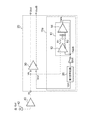
まず、PON方式の通信システムについて説明する。図1(a)は、PON方式のブロック図である。局舎80内の局側通信装置82は、複数の家庭70aから70c内の各家庭側通信装置72と光ファイバである通信経路L1およびL2を介し接続されている。局側通信装置82とオプティカルスプリッタ74とは1本の通信経路L1で接続されている。オプティカルスプリッタ74と各家庭側通信装置72との間は各通信経路L2を介し接続されている。オプティカルスプリッタ74は、各家庭側通信装置72から各通信経路L2を介し入出力された信号を通信経路L1に結合する。通信経路L1の信号は局側通信装置82に入出力される。局側通信装置82は制御回路84、送信部86および受信部88を有している。送信部86は、各家庭側通信装置72に光信号を送信する送信回路である。受信部88は、各家庭側通信装置72からの光信号を受信する受信回路である。制御回路84は送信部86および受信部88を制御する回路であり、例えば、受信部88にリセット信号を出力する。
First, a PON communication system will be described. FIG. 1A is a block diagram of the PON system. The station
図1(b)は、受信部88の受光素子(図2のフォトダイオード42参照)に入力される光信号を時間に対し示す模式図である。期間Ton1の間は家庭70aの家庭側通信装置72からの光信号が入力される。期間Toff1の間は光信号は入力されず、期間Ton2において家庭70bの家庭側通信装置(不図示)からの光信号が入力される。さらに、期間Toff2の間は光信号は入力されず、期間Ton3において家庭70cの家庭側通信装置(不図示)からの光信号が入力される。各家庭側通信装置72の出力信号の振幅および各通信経路L2での光信号の損失はそれぞれ異なる。このため、期間Ton1、Ton2およびTon3の光信号の振幅はそれぞれ振幅A1、A2およびA3と異なる。このように、PON用のPD12には、異なる家庭から光信号が異なる振幅で不定期に入力される。なお、期間Toff1およびToff2は通信経路L2を切り換える期間である。
FIG. 1B is a schematic diagram showing an optical signal input to the light receiving element (see the
次に比較例について説明する。図2は、比較例に係る電子回路のブロック図である。図2を参照に、フォトダイオード(PD)42の出力電流を増幅したTIA40の出力電圧信号がデジタル入力信号VAとして電子回路90に入力される。電子回路90は差動増幅回路30および参照信号生成回路11を有している。差動増幅回路30は、入力信号VAが入力する入力端子と参照信号Vrefが入力する参照信号端子を有している。差動増幅回路30は入力信号VAと参照信号Vrefとを差動増幅し、差動出力信号VoutおよびVoutBを出力する。このように、差動増幅回路30は、デジタル情報を含んだ高周波信号であるデジタル入力信号VAを参照信号Vrefと比較することで、パルス信号に変換するパルス変換回路である。
Next, a comparative example will be described. FIG. 2 is a block diagram of an electronic circuit according to a comparative example. Referring to FIG. 2, the output voltage signal of
参照信号生成回路11は、平均化回路10と第1保持回路20とを有している。平均化回路10は、入力信号VAを平均化し平均化信号Vsmを出力する。平均化回路10は、差動増幅回路12、14、抵抗R1、R2およびキャパシタC1を有する。差動増幅回路12には入力信号VAと差動増幅回路14の出力ノードNsmの平均化信号Vsmとが入力する。差動増幅回路12は入力信号VAと平均化信号Vsmとを差動増幅し、差動信号を抵抗R1およびR2を介し差動増幅回路14に出力する。差動増幅回路14の2つの入力はキャパシタC1により互いに接続されている。平均化回路10は、入力信号VAを、抵抗R1、R2およびキャパシタC1で規定される時定数により平均化し、平均化信号Vsmを出力ノードNsmに出力する。
The reference
第1保持回路20は、差動増幅回路30の参照信号端子と平均化回路10との間に接続されている。第1保持回路20は、例えばピークホールド回路であり、平均化信号Vsmを保持し、保持信号Vphを差動増幅回路30の参照信号端子に出力する。例えば、第1保持回路20は、平均化信号Vsmのピーク付近の信号を保持し保持信号Vphとして出力する。保持信号Vphは参照信号Vrefとして差動増幅回路30に入力される。
The
平均化回路10および第1保持回路20の機能について説明する。図3(a)及び図3(b)は、時間に対する入力信号VAと参照信号Vrefとを示した図である。図3(a)及び図3(b)を参照に、期間Toffにおいて、PD42に光信号は入力されない。よって、入力信号VAは初期値である。期間Tonにおいて、PD42に光信号が入力され、入力信号VAが変動する。ある一定期間(通信準備期間Tpre)においては、オン、オフ信号(0、1信号)が交互に入力される。通信準備期間Tpreは、平均化回路10が入力信号VAを平均化するための準備期間である。通信準備期間Tpre以降は実際にデータが送信される通信期間Tcomである。通信期間Tcomにおいて、入力信号VAは、オン、オフ信号が交互に入力されるとは限らないが、以降の図では、オン、オフ信号が交互に入力される場合を記載する。
The functions of the averaging
差動増幅回路30は、参照信号Vrefに対し入力信号VAが大きいか小さいかでハイレベルまたはローレベルを出力信号Vout及びVoutBとして出力する。このため、参照信号Vrefは早期に、入力信号VAの平均値Vmとなることが好ましい。しかしながら、図3(a)のように、平均化回路10の時定数が長いと、参照信号Vrefは早期には平均値Vmとはならない。このように、通信準備期間Tpre内に参照信号Vrefが安定化しない。一方、図3(b)のように、平均化回路10の時定数が短いと、参照信号Vrefは通信準備期間Tpre内に早期に平均値Vmとなるが、その後、入力信号VAの変動に同期し参照信号Vrefも変動してしまう。
The
図4は比較例の入力信号VAと参照信号Vrefとを示した図である。図4を参照に、平均化回路10の時定数を図3(b)のように短くする。また、第1保持回路20の保持の時定数を平均化回路10の時定数より十分長くする。これにより、参照信号Vrefは入力信号VAに追従し早期に立ち上がる。入力信号VAがローレベルの場合も、第1保持回路20が平均化信号Vsmのピーク付近の保持信号Vphを出力するため、図3(b)のような参照信号Vrefの時間に対する変動は小さく、通信準備期間Tpre内に参照信号Vrefは早期に入力信号VAの平均値Vmに達し安定する。
FIG. 4 is a diagram showing the input signal VA and the reference signal Vref of the comparative example. Referring to FIG. 4, the time constant of the averaging
しかしながら、比較例の参照信号生成回路11においては、参照信号Vrefが安定した後の通信期間Tcomにおいて、入力光信号のレベル変動があると、その影響を受けることにより、第1保持回路20に入力する平均化信号Vsmが変動すると、第1保持回路20は平均化信号Vsmのピークを保持してしまう。また、第1保持回路20から平均化回路10側への放電等によっても保持信号Vphが変動し参照信号Vrefが変動してしまう。例えば、通信期間Tcomにおいて、入力信号VAの出力レベルが大きくなった場合には、それらにつられて平均化信号Vsmも大きくなり、保持信号Vphも大きくなってしまう。
However, in the reference
表1は本発明の原理を示す表である。本発明によれば、参照信号生成回路11は、入力信号VAを平均化した平均化信号Vsmを参照信号Vrefとし、その後、入力信号VAによらず平均化信号Vsmを保持した保持信号Vphを参照信号Vrefとする。例えば、通信準備期間Tpreにおいて、平均化信号Vsmを参照信号Vrefとする。これにより、参照信号Vrefを入力信号VAの平均値とすることができる。一方、通信期間Tcom(通信準備期間の後)は入力信号VAによらず平均化信号Vsmを保持した保持信号Vphを参照信号Vrefとする。つまり、通信期間においては、保持信号Vphは入力信号VAに依存しない。これにより、参照信号Vrefを入力信号VAの平均値に保持したままとすることができ、入力信号VAの影響で参照信号Vrefが変動することを抑制することができる。

通信準備期間Tpreにおいて、参照信号生成回路11が入力信号VAを平均化し平均化信号Vsmとする。よって、参照信号生成回路11は、入力信号VAを平均化し平均化信号とした際の平均化信号Vsmのピークを保持し参照信号Vrefとすることが好ましい。
In the communication preparation period Tpre, the reference
なお、表1では通信準備期間Tpreと通信期間Tcomとで参照信号Vrefを切り換えている。参照信号Vrefの切り換えのタイミングは、参照信号Vrefが入力信号VAの平均値に安定した後または入力信号VAの平均値に近づけばよく、通信期間Tcomの前であることで通信期間中のVrefは安定する。以下、表1に示した参照信号生成回路11を実現する実施例について説明する。
In Table 1, the reference signal Vref is switched between the communication preparation period Tpre and the communication period Tcom. The reference signal Vref may be switched after the reference signal Vref is stabilized to the average value of the input signal VA or close to the average value of the input signal VA, and before the communication period Tcom, Vref during the communication period is Stabilize. Hereinafter, an embodiment for realizing the reference
図5は実施例1に係る電子回路のブロック図である。図5を参照に、実施例1の参照信号生成回路11aは、平均化回路10の出力ノードNsmと第1保持回路20との間に第1スイッチSW1が設けられている。つまり、第1スイッチSW1は、平均化信号Vsmを第1保持回路20aに接続または遮断する。その他の構成は比較例の図2と同じであり説明を省略する。
FIG. 5 is a block diagram of an electronic circuit according to the first embodiment. Referring to FIG. 5, in the reference
図6(a)は、第1保持回路20としてローパスフィルタを用いる例を示す図である。図6(a)を参照に、第1保持回路20aは、入力と出力との間の抵抗Rと、出力とグランドとの間のキャパシタCと、を有している。このように、第1保持回路20aとして時定数が平均化回路10の時定数より十分大きなローパスフィルタを用いることができる。
FIG. 6A is a diagram illustrating an example in which a low-pass filter is used as the
図6(b)は、第1保持回路20としてピークホールド回路を用いる例を示す図である。図6(b)を参照に、第1保持回路20は差動増幅回路22、24、ダイオードD1、キャパシタC2及びリセット回路25を有している。差動増幅回路22は、平均化信号Vsmと保持信号Vphとを差動増幅する。差動増幅回路22の出力はダイオードD1のアノードに接続する。ダイオードD1のカソードは差動増幅回路24の入力に接続される。差動増幅回路24は、信号Vpと保持信号Vphとを差動増幅し保持信号Vphを出力する。ダイオードD1のカソードとグランドとの間には、キャパシタC2とリセット回路25とが並列に接続される。リセット回路25はNPNバイポーラトランジスタ26である。トランジスタ26のコレクタがダイオードD1のカソードに、エミッタがグランドに接続され、ベースにリセット信号Resetが入力される。リセット信号Resetがハイレベルになると、第1保持回路20は、保持信号Vphを一定値(例えばグランド)に設定する。これにより、第1保持回路20がリセットされる。
FIG. 6B is a diagram illustrating an example in which a peak hold circuit is used as the
平均化信号Vsmが保持信号Vphより大きいと、差動増幅回路22は正の信号を出力し、ダイオードD1を介しキャパシタC2を充電し、信号Vpの電位が定まる。差動増幅回路24は信号Vsmと保持信号Vphとを差動増幅する。よって、保持信号Vphは信号Vpとなる。信号Vsmが保持信号Vphより小さいと、差動増幅回路22は負の信号を出力するが、ダイオードD1は逆方向のため、信号Vpは変化しない。以上により、ピークホールド回路である第1保持回路20は、平均化信号Vsmの極大値(ピーク)に保持信号Vphを保持する。
When the average signal Vsm is larger than the hold signal Vph, the
図7は、実施例1に係る電子回路の動作を示すタイムチャートである。時間に対する入力信号VAおよび参照信号Vref並びに第1スイッチSW1の動作を示している。図7を参照に、入力信号VAが入力する時点t0では第1スイッチSW1はオン状態である。よって、通信準備期間Tpreの当初は、比較例の図4で説明した動作と同様に、参照信号Vrefは早期に入力信号VAの平均値となり安定する。参照信号Vrefが安定した時点の時間t1の後、時間t2に第1スイッチSW1がオフする。これにより、通信準備期間Tpreが終了した以降は、第1スイッチSW1がオフする前に第1保持回路20が保持した保持信号Vphが参照信号Vrefとなるため、平均化信号Vsmが参照信号Vrefに影響することを抑制することができる。たとえ、時間t1の前にスイッチSW1がオフしたとしても、参照信号Vrefが安定レベルに近づいていれば平均化信号Vsmが参照信号Vrefに影響することを抑制することができる。
FIG. 7 is a time chart illustrating the operation of the electronic circuit according to the first embodiment. The operation of the input signal VA and the reference signal Vref with respect to time and the first switch SW1 is shown. Referring to FIG. 7, at time t0 when the input signal VA is input, the first switch SW1 is in the on state. Therefore, at the beginning of the communication preparation period Tpre, the reference signal Vref becomes an average value of the input signal VA at an early stage and becomes stable, similarly to the operation described in the comparative example of FIG. After time t1 when the reference signal Vref is stabilized, the first switch SW1 is turned off at time t2. Thus, after the communication preparation period Tpre ends, the holding signal Vph held by the
実施例1によれば、図7のように、第1スイッチSW1は、時間t2までの期間において(つまり、通信準備期間Tpreの少なくても一部の期間において)平均化信号Tsmを第1保持回路20に接続する。これにより、表1のように、参照信号生成回路11aは、入力信号VAを平均化した平均化信号Vsmを保持し参照信号Vrefとする。また、第1保持回路20が平均化信号Vsmを保持した保持信号Vphを参照信号Vrefとするため、図4で説明したように、参照信号Vrefを早期に入力信号VAの平均値近くに安定化させることができる。一方、図7のように、第1スイッチSW1は、時間t2以降の期間(つまり、通信準備期間Tpre以降の通信期間Tcom)は、平均化信号Vsmと第1保持回路20とを遮断する。これにより、表1のように、入力信号VAによらず平均化信号Vsmを保持した保持信号Vphを参照信号Vrefとする。よって、入力信号VAの影響で参照信号Vrefが変動することを抑制することができる。
According to the first embodiment, as illustrated in FIG. 7, the first switch SW1 holds the average signal Tsm for the first time in the period up to the time t2 (that is, in at least a part of the communication preparation period Tpre). Connect to
さらに、第1保持回路20がリセット可能であることにより、図1(b)の期間Toff1およびToff2に第1保持回路20をリセットし、参照信号Vrefを最小値にセットすることができる。
Further, since the
実施例2は第2スイッチSW2を有する例である。図8は実施例2のブロック図である。図8を参照に、実施例2の参照信号生成回路11bは、平均化信号Vsmと保持信号Vphとのいずれかを選択し参照信号Vrefとする第2スイッチSW2を有している。つまり、第2スイッチSW2は、第1保持回路20の出力、および平均化回路10の出力と第1スイッチSW1との間の出力ノードNsmのいずれかを選択的に差動増幅回路30の参照信号端子に接続する。その他の構成は、実施例1の図5と同じであり、説明を省略する。
The second embodiment is an example having the second switch SW2. FIG. 8 is a block diagram of the second embodiment. Referring to FIG. 8, the reference
図9は、実施例2に係る電子回路の動作を示すタイムチャートである。時間に対する入力信号VAおよび参照信号Vref並びに第1スイッチSW1および第2スイッチSW2の動作を示している。図9を参照に、時間t2以前では、第2スイッチSW2は平均化信号Vsmを選択し参照信号Vrefとする。時間t2以降では、スイッチSW2は保持信号Vphを選択し参照信号Vrefとする。 FIG. 9 is a time chart illustrating the operation of the electronic circuit according to the second embodiment. The operations of the input signal VA and the reference signal Vref with respect to time, and the first switch SW1 and the second switch SW2 are shown. Referring to FIG. 9, before time t2, second switch SW2 selects averaged signal Vsm as reference signal Vref. After time t2, the switch SW2 selects the holding signal Vph and sets it as the reference signal Vref.
実施例2によれば、図9のように、第2スイッチSW2は、時間t2以前(通信準備期間Tpreの初期)において、平均化信号Vsmを選択する。つまり、出力ノードNsmを選択し差動増幅回路30の参照信号端子に接続する。これにより、表1のように、参照信号生成回路11bは、入力信号VAを平均化した平均化信号Vsmを参照信号Vrefとすることができる。このとき、第1スイッチSW1は、オン状態になっており、第1保持回路20には、平均化信号Vsmが入力されている。一方、第2スイッチSW2は、時間t2以降(通信準備期間Tpreの後)は、保持信号Vphを選択する。つまり、第1保持回路20の出力を選択し差動増幅回路30の参照信号端子に接続する。時間t2以降は、第1スイッチSW1がオフとなっており、第1保持回路20には、時間t2までの平均化信号Vsmの例えばピーク値が保持されている。これにより、表1のように、入力信号VAによらず平均化信号Vsmを保持した保持信号Vphを参照信号Vrefとすることができる。よって、入力信号VAの影響で参照信号Vrefが変動することを抑制することができる。
According to the second embodiment, as illustrated in FIG. 9, the second switch SW2 selects the averaged signal Vsm before time t2 (initial stage of the communication preparation period Tpre). That is, the output node Nsm is selected and connected to the reference signal terminal of the
実施例3は、参照信号生成回路が第2保持回路を有する例である。図10は、実施例3のブロック図である。図10を参照に、実施例3の参照信号生成回路11cは、平均化信号Vsmを保持する第2保持回路32を有している。つまり、第2保持回路32は、出力ノードNsmと第2スイッチSW2の間に接続されている。第2スイッチSW2は、第2保持回路32が保持した平均化信号Vsm2と保持信号Vphとのいずれかを選択し、選択した信号を参照信号Vrefとする。その他の構成は、実施例2の図8と同じであり、説明を省略する。
The third embodiment is an example in which the reference signal generation circuit includes a second holding circuit. FIG. 10 is a block diagram of the third embodiment. Referring to FIG. 10, the reference
実施例3の第1スイッチSW1および第2スイッチSW2の動作は、実施例2の図9と同じである。実施例3によれば、通信準備期間Tpreにおいて、第2スイッチSW2は、第2保持回路32が保持した平均化信号Vsm2を参照信号Vrefとする。これにより、通信準備期間Tpreにおいて、参照信号Vrefをより早く安定化させることができる。なお、第2保持回路32の時定数は、通信準備期間Tpreにおけるオフの間には、平均化信号Vsmを保持すればよいため、第1保持回路20の時定数より小さいことが好ましい。このように、通信準備期間Tpreと通信期間Tcomとの保持時間を独立に設定することができる。また、第2保持回路32としては、図6(a)のようなローパスフィルタまたは図6(b)のようなピークホールド回路を用いることができる。
The operations of the first switch SW1 and the second switch SW2 of the third embodiment are the same as those in FIG. 9 of the second embodiment. According to the third embodiment, in the communication preparation period Tpre, the second switch SW2 uses the average signal Vsm2 held by the
図11は実施例4に係る電子回路のブロック図である。図11を参照に、参照信号生成回路11dは、平均化回路10a、第1保持回路36、第1スイッチSW1および第2保持回路34を有している。平均化回路10aは、差動増幅回路12aおよび14、抵抗R1、R2およびキャパシタC1を有している。差動増幅回路23aの正側の入力が+1と+2との2つあり、第2スイッチ信号Vsw2により、入力+1または+2を選択することができる。その他の差動増幅回路12aおよび14、抵抗R1、R2およびキャパシタC1の構成は実施例1〜3の平均化回路10と同じであり説明を省略する。平均化回路10aの出力Vsm(平均化信号)は、第2保持回路34に入力する。第2保持回路34は平均化信号Vsmを保持し(例えば、平均化信号Vsmのピークを保持し)保持信号Vphを第1スイッチSW1を介し第1保持回路36に出力する。また第2保持回路34はVphを差動増幅回路30の参照信号端子に出力する。平均化回路10aの入力+1には、入力信号VAが入力し、入力+2には、第1保持回路36の出力Vph2が入力する。よって、平均化回路10aは、入力信号VAおよび第1保持回路36の出力Vph2のいずれかを選択して平均化することにより平均化信号Vsmを生成することができる。
FIG. 11 is a block diagram of an electronic circuit according to the fourth embodiment. Referring to FIG. 11, the reference
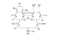
図12は、差動増幅回路12aの回路図である。図12を参照に、差動増幅回路12aは、NPNトランジスタT1〜T6、抵抗R8、R9および電流源110を有している。第2スイッチ信号Vsw2とVsw2Bとは補信号である。第2スイッチ信号Vsw2がハイの場合、トランジスタT1、T2、抵抗R8およびR9からなる差動回路が活性化し、参照信号Vrefと入力+1の差動信号OutおよびOutBが出力される。第2スイッチ信号Vsw2がローの場合、トランジスタT3、T4、抵抗R8およびR9からなる差動回路が活性化し、参照信号Vrefと入力+2の差動信号OutおよびOutBが出力される。このように、トランジスタT5およびT6は入力+1と+2との選択する第2スイッチSW2として機能する。
FIG. 12 is a circuit diagram of the
図13は、実施例4に係る電子回路の動作を示すタイムチャートである。時間に対する入力信号VAおよび参照信号Vref並びに第1スイッチSW1および第2スイッチSW2の動作を示している。図13を参照に、時間t0では、第2スイッチSW2は入力信号VAを選択し、第1スイッチSW1はオンしている。参照信号Vrefは第2保持回路34により、早期に安定することができる。また、第1スイッチSW1がオンしているため、第1保持回路36に保持信号Vphが保持される。時間t1において、参照信号Vrefが安定した後の時間t2に第1スイッチSW1がオフする。第2スイッチSW2が入力信号VAから第1保持回路36の出力Vph2に切り換わる。言い換えれば、差動増幅回路12aは入力を+1から+2に切り換える。これにより、平均化回路10aは出力Vph2を平均化する。
FIG. 13 is a time chart illustrating the operation of the electronic circuit according to the fourth embodiment. The operations of the input signal VA and the reference signal Vref with respect to time, and the first switch SW1 and the second switch SW2 are shown. Referring to FIG. 13, at time t0, the second switch SW2 selects the input signal VA, and the first switch SW1 is on. The reference signal Vref can be stabilized early by the
実施例4によれば、第2スイッチSW2が入力信号VAを選択すると、平均化回路10aは、入力信号VAの平均化により平均化信号Vsmを生成する。このとき第1スイッチSW1がオンしているため、第1保持回路36は、平均化信号Vsmを保持しVph2を出力する。第1保持回路36の出力Vph2は平均化回路10aに入力する。第2スイッチSW2が第1保持回路36の出力Vph2を選択すると、平均化回路10aを介した第1保持回路36の出力Vph2が差動増幅回路30の参照信号端子に出力される。
According to the fourth embodiment, when the second switch SW2 selects the input signal VA, the averaging
実施例4によれば、通信準備期間Tpreにおいて、第1スイッチSW1はオンし第1保持回路36と平均化回路10aとを接続する。平均化回路10aは入力信号VAを選択し平均化することとにより平均化信号Vsmを生成する。これにより、表1のように、参照信号生成回路11dの出力である参照信号Vrefは、入力信号VAを平均化した信号となる。一方、通信準備期間Tpreの後、第1スイッチSW1はオフし第1保持回路36と平均化回路10aとを遮断する。平均化回路10aは第1保持回路36の出力Vph2を選択し平均化することとにより平均化信号Vsmを生成する。これにより、参照信号Vrefは、第1保持回路36の出力Vph2を平均化した信号となる。つまり、参照信号Vrefは、表1のように、入力信号VAによらず、第1保持回路36が平均化信号Vsmを保持した保持信号(出力Vph2)となる。よって、入力信号VAの影響で参照信号Vrefが変動することを抑制することができる。
According to the fourth embodiment, in the communication preparation period Tpre, the first switch SW1 is turned on to connect the
さらに、平均化回路10aの出力と第1スイッチSW1との間に第2保持回路34が接続されている。第2保持回路34は、平均化信号Vsmを保持し参照信号端子および第1スイッチSW1に出力する。つまり、第2保持回路34と第1スイッチSW1との間のノード(保持ノード)が差動増幅回路30の参照信号端子に接続されている。第1保持回路36は第2保持回路34に保持された平均化信号を保持する。これにより、通信準備期間Tpreにおいても第2保持回路34が入力信号VAの平均化信号を保持し参照信号とするため、参照信号Vrefを早期に安定化させることができる。通信準備期間Tpreにおける時定数は入力信号VAのオンオフの期間に対し長い時間であればよく、通信期間Tcomにおける時定数は期間Tonに対し長い時間であることが好ましい。よって、第1保持回路36の時定数は第2保持回路34の時定数より長いことが好ましい。また、比較例と同様に、平均化回路10aの平均化の時定数は第2保持回路34の時定数より短いことが好ましい。このように、通信準備期間Tpreにおいて参照信号Vrefを安定化させる時定数と通信期間Tcomにおいて参照信号を安定に保つ時定数を独立に設定することができる。
Further, a
第1保持回路36および第2保持回路34は、例えば図6(a)のローパスフィルタとすることができる。また、例えば、図6(b)のピークホールド回路とすることができる。
The
図14は実施例5のブロック図である。図14を参照に、実施例4の図11に比較し、差動増幅回路30の後段に差動増幅回路92および94が設けられている。これにより、実施例4より大きな出力を行うことができる。また、差動増幅回路92または94をリミットアンプとすることにより、差動出力信号VoutおよびVoutBを矩形波とすることができる。第1保持回路36および第2保持回路34は、図6(b)のピークホールド回路を用いている。
FIG. 14 is a block diagram of the fifth embodiment. Referring to FIG. 14, as compared with FIG. 11 of the fourth embodiment,
制御回路102は、抵抗R5、R6、ピークホールド回路56、ヒステリシス比較器54、AND回路58、62、タイマー60および増幅回路64を有している。差動増幅回路30の出力信号A3+、A3−の間に抵抗R5、R6が接続されている。ピークホールド回路56は、信号A3+のピークを保持し、ヒステリシス比較器54に出力する。抵抗R5とR6とで抵抗分割された信号がヒステリシス比較器54の他方の入力に入力する。ヒステリシス比較器54は、信号A3+が信号A3+の極大値の一定割合以下となると信号SDとしてローレベルを出力する。増幅回路64は信号SDを増幅する。
The control circuit 102 includes resistors R5 and R6, a
AND回路58にはリセット信号Resetの反転と信号SDが入力する。よって、AND回路58は、リセット信号Resetがローレベル(リセットをしていない)でかつ信号SDがハイレベルのとき信号SELとしてハイレベルを出力する。AND回路62には、信号SELと信号SELをタイマー60で遅延させた信号とが入力する。AND回路62は、信号SELがローレベルとなって、一定時間後にローレベルを出力する。これにより、第1スイッチ信号Vsw1および第2スイッチ信号Vsw2としてローレベルが出力される。増幅回路64は第1スイッチ信号Vsw1を増幅する。第2スイッチSW2は第2スイッチ信号Vsw2がハイレベルのときVAを選択し、ローレベルのときVph2を選択する。第1スイッチSW1は、第1スイッチ信号Vsw1がハイレベルのときオンし、ローレベルのときオフする。
The AND
増幅回路52はリセット信号Resetを増幅する。リセット信号Resetはハイレベルとなると対応する回路をリセットする信号である。増幅回路52の出力は、ピークホールド回路56、第1保持回路36および第2保持回路34に入力する。リセット信号Resetがハイレベルになると、ピークホールド回路56、第1保持回路36および第2保持回路34はリセットされ、ピークホールド回路56、第1保持回路36および第2保持回路34がそれぞれ保持していた保持信号はリセットされる。
The
図15は実施例5に係る電子回路の動作を示すタイムチャートである。時間に対する入力信号VA、Reset信号、スイッチ信号Vsw1、Vsw2、第1スイッチSW1の動作、第2スイッチSW2の動作および参照信号Vrefを示している。前の入力信号VAが入力される期間Ton2では、Reset信号はロー、スイッチ信号Vsw1およびVsw2はローである。第2スイッチSW2はVph2を選択しており、参照信号VrefはVph2の平均値のピークとなっている。第1スイッチSW1はオフである。入力信号VAが入力されない期間Toff2において、リセット信号Resetがハイレベルとなる。第1保持回路36、第2保持回路34およびピークホールド回路56がリセットされる。これにより、A3+はA3+の極大値の一定割合以上となるため、信号SDはハイレベルとなる。よって、信号SELもハイレベルとなり、スイッチ信号Vsw1およびVsw2はハイレベルとなる。これにより、第1スイッチSW1はオン、第2スイッチSW2はVAを選択し、参照信号Vrefは入力信号VAの平均値のピークとなる。
FIG. 15 is a time chart illustrating the operation of the electronic circuit according to the fifth embodiment. An input signal VA, a Reset signal, switch signals Vsw1, Vsw2, operation of the first switch SW1, operation of the second switch SW2, and reference signal Vref with respect to time are shown. In the period Ton2 in which the previous input signal VA is input, the Reset signal is low and the switch signals Vsw1 and Vsw2 are low. The second switch SW2 selects Vph2, and the reference signal Vref has a peak of the average value of Vph2. The first switch SW1 is off. In a period Toff2 in which the input signal VA is not input, the reset signal Reset is at a high level. The
時間t0において、期間Ton3となり入力信号VAが入力しはじめる。時間t0において、参照信号Vrefは0(最小値)のため、A3+は極大値となる。参照信号Vrefが大きくなるにつれ、A3+は極大値に対するA3+の割合は小さくなる。時間t4において、A3+の極大値に対するA3+の割合が一定値以下になると、信号SDはロ−レベルになる。ここで、ヒステリシス比較器54の時定数を入力信号VAの周期より長くすることにより、信号SAは入力信号VAの周期の影響を受けない。時間t4において、信号SELがローレベルとなる。タイマー60による遅延時間Tdel後の時間t2において、スイッチ信号Vsw1およびVsw2がローレベルとなる。これにより、第1スイッチSW1はオフ、第2スイッチSW2はVph2を選択し、参照信号VrefはVph2の平均値のピークとなる。
At time t0, the period Ton3 is reached and the input signal VA starts to be input. Since the reference signal Vref is 0 (minimum value) at time t0, A3 + becomes a maximum value. As the reference signal Vref increases, the ratio of A3 + to the maximum value of A3 + decreases. At time t4, when the ratio of A3 + to the maximum value of A3 + becomes equal to or less than a certain value, the signal SD becomes low level. Here, by making the time constant of the
以上のように、実例例5の回路により実施例4の図13で説明した動作が可能となる。抵抗R5およびR6は、参照信号Vrefが平均値Vmとなる直前に信号SDがハイレベルとなるように設定することが好ましい。タイマー60の遅延時間は、参照信号Vrefが安定してから、通信準備期間Tpreが終了するまでの間にスイッチ信号Vsw2およびVsw1がオフするように設定することが好ましい。
As described above, the operation described with reference to FIG. The resistors R5 and R6 are preferably set so that the signal SD becomes high level immediately before the reference signal Vref becomes the average value Vm. The delay time of the
以上、本発明の実施例について詳述したが、本発明は係る特定の実施例に限定されるものではなく、特許請求の範囲に記載された本発明の要旨の範囲内において、種々の変形・変更が可能である。 Although the embodiments of the present invention have been described in detail above, the present invention is not limited to such specific embodiments, and various modifications and changes can be made within the scope of the gist of the present invention described in the claims. It can be changed.
10 平均化回路
11 参照信号生成回路
20、34 第1保持回路
30 差動増幅回路
32、36 第2保持回路
40 トランスインピーダンスアンプ
42 フォトダイオード
SW1 第1スイッチ
SW2 第2スイッチ
DESCRIPTION OF
Claims (9)
前記入力信号を平均化し平均化信号を生成する平均化回路と、
前記参照信号端子と前記平均化回路の出力との間に設けられ、前記平均化信号を保持し前記参照信号端子に出力する第1保持回路と、
前記第1保持回路と前記平均化回路との間に設けられた第1スイッチと、
前記記第1保持回路の出力、および前記平均化回路の出力と前記第1スイッチとの間の出力ノードのいずれかを選択的に前記参照信号端子に接続する第2スイッチと、
前記出力ノードと前記第2スイッチとの間に接続され、前記平均化信号を保持し前記第2スイッチに出力する第2保持回路と、
を備えることを特徴とする電子回路。 A differential amplifier circuit having an input terminal to which an input signal is input and a reference signal terminal;
An averaging circuit that averages the input signal to generate an averaged signal;
A first holding circuit which is provided between the reference signal terminal and the output of the averaging circuit, holds the averaged signal and outputs the averaged signal to the reference signal terminal;
A first switch provided between the first holding circuit and the averaging circuit;
A second switch for selectively connecting one of the output of the first holding circuit and the output node between the output of the averaging circuit and the first switch to the reference signal terminal;
A second holding circuit connected between the output node and the second switch, holding the averaged signal and outputting it to the second switch;
An electronic circuit comprising:
前記第2スイッチは、前記通信準備期間において前記出力ノードを選択し前記参照信号端子に接続し、前記通信準備期間の後は前記第1保持回路の出力を選択し前記参照信号端子に接続することを特徴とする請求項1記載の電子回路。 The first switch connects the first holding circuit and the averaging circuit in a communication preparation period for averaging the input signals, and after the communication preparation period, the first holding circuit and the average Shut off the circuit
The second switch selects the output node in the communication preparation period and connects it to the reference signal terminal, and after the communication preparation period, selects the output of the first holding circuit and connects it to the reference signal terminal. The electronic circuit according to claim 1 .
前記入力信号を平均化し平均化信号を生成する平均化回路と、
前記参照信号端子と前記平均化回路の出力との間に設けられ、前記平均化信号を保持し前記参照信号端子に出力する第1保持回路と、
前記第1保持回路と前記平均化回路との間に設けられた第1スイッチと、
を具備し、
前記第1保持回路の出力は前記平均化回路に入力され、前記平均化回路を介した前記第1保持回路の出力が前記参照信号端子に出力されることを特徴とする電子回路。 A differential amplifier circuit having an input terminal to which an input signal is input and a reference signal terminal;
An averaging circuit that averages the input signal to generate an averaged signal;
A first holding circuit which is provided between the reference signal terminal and the output of the averaging circuit, holds the averaged signal and outputs the averaged signal to the reference signal terminal;
A first switch provided between the first holding circuit and the averaging circuit;
Comprising
The output of the first holding circuit is input to the averaging circuit, an electronic circuit which the output of the first holding circuit through the averaging circuit is characterized in that it is output to the reference signal terminal.
前記平均化回路は、前記通信準備期間において前記入力信号を選択し平均化することにより前記平均化信号を生成し、前記通信準備期間の後は前記第1保持回路の出力を選択することにより前記平均化信号を生成することを特徴とする請求項5記載の電子回路。 The first switch connects the first holding circuit and the averaging circuit in a communication preparation period for averaging the input signals, and after the communication preparation period, the first holding circuit and the average Shut off the circuit
The averaging circuit generates the averaged signal by selecting and averaging the input signal in the communication preparation period, and selecting the output of the first holding circuit after the communication preparation period 6. The electronic circuit according to claim 5 , wherein an averaged signal is generated.
前記第1保持回路は前記第2保持回路で保持された前記平均化信号を保持することを特徴とする請求項6記載の電子回路。 The average signal is held between the output of the averaging circuit and the first switch, and the output is connected to the reference signal terminal after the communication preparation period, and the output is connected during the communication preparation period. A second holding circuit connected to the first switch is provided;
The electronic circuit according to claim 6, wherein the first holding circuit holds the average signal held by the second holding circuit.
Priority Applications (1)
| Application Number | Priority Date | Filing Date | Title |
|---|---|---|---|
| JP2008221221A JP5215087B2 (en) | 2008-08-29 | 2008-08-29 | Electronic circuit |
Applications Claiming Priority (1)
| Application Number | Priority Date | Filing Date | Title |
|---|---|---|---|
| JP2008221221A JP5215087B2 (en) | 2008-08-29 | 2008-08-29 | Electronic circuit |
Publications (3)
| Publication Number | Publication Date |
|---|---|
| JP2010057014A JP2010057014A (en) | 2010-03-11 |
| JP2010057014A5 JP2010057014A5 (en) | 2011-09-29 |
| JP5215087B2 true JP5215087B2 (en) | 2013-06-19 |
Family
ID=42072433
Family Applications (1)
| Application Number | Title | Priority Date | Filing Date |
|---|---|---|---|
| JP2008221221A Active JP5215087B2 (en) | 2008-08-29 | 2008-08-29 | Electronic circuit |
Country Status (1)
| Country | Link |
|---|---|
| JP (1) | JP5215087B2 (en) |
Families Citing this family (3)
| Publication number | Priority date | Publication date | Assignee | Title |
|---|---|---|---|---|
| US8390383B2 (en) | 2010-06-24 | 2013-03-05 | Sumitomo Electric Industries, Ltd. | Amplifier for receiving intermittent optical signal |
| JP5494285B2 (en) | 2010-06-24 | 2014-05-14 | 住友電気工業株式会社 | Electronic circuit |
| JP5696940B2 (en) * | 2011-08-05 | 2015-04-08 | 日本電信電話株式会社 | Light intensity control device |
Family Cites Families (3)
| Publication number | Priority date | Publication date | Assignee | Title |
|---|---|---|---|---|
| JPS54118148A (en) * | 1978-03-07 | 1979-09-13 | Nec Corp | Comparator circuit |
| JP3655770B2 (en) * | 1999-03-29 | 2005-06-02 | 日本電気株式会社 | Optical receiver circuit |
| JP5101131B2 (en) * | 2007-02-23 | 2012-12-19 | 住友電工デバイス・イノベーション株式会社 | Electronic circuit |
-
2008
- 2008-08-29 JP JP2008221221A patent/JP5215087B2/en active Active
Also Published As
| Publication number | Publication date |
|---|---|
| JP2010057014A (en) | 2010-03-11 |
Similar Documents
| Publication | Publication Date | Title |
|---|---|---|
| JP5280256B2 (en) | Electronic circuit | |
| JP5494285B2 (en) | Electronic circuit | |
| JP4927664B2 (en) | Preamplifier circuit | |
| JP5725168B2 (en) | Detection device, optical receiver, detection method, and optical reception method | |
| US20080309407A1 (en) | Transimpedance Amplifier | |
| US7755434B2 (en) | Electronic circuit | |
| JP5305932B2 (en) | Preamplifier | |
| JP2008211702A (en) | Pre-amplifier and optical receiving device using the same | |
| JP2015186013A (en) | transimpedance amplifier | |
| CN103229435B (en) | Optical receiver | |
| JP2008236455A (en) | Transimpedance amplifier and control method of transimpedance amplifier | |
| JP5215087B2 (en) | Electronic circuit | |
| JP5488357B2 (en) | Amplifier circuit | |
| WO2006013841A1 (en) | Receiving method and receiving circuit | |
| JP5101131B2 (en) | Electronic circuit | |
| CN110785949B (en) | Optical receiver | |
| US8390383B2 (en) | Amplifier for receiving intermittent optical signal | |
| JP3816895B2 (en) | Burst mode optical receiver with signal level detector | |
| JP2009177577A (en) | Burst signal reception method, burst signal receiver, station side terminal, and pon system | |
| KR100601048B1 (en) | Receiver for burst mode packet and Method for receiving the packet | |
| JP5512040B2 (en) | Bandwidth variable amplifier | |
| JP2001211040A (en) | Digital signal amplifying circuit and optical receiving circuit | |
| JP4590708B2 (en) | Optical receiver circuit | |
| JP2008211375A (en) | Electronic circuit | |
| WO2020225893A1 (en) | Transimpedance amplifier |
Legal Events
| Date | Code | Title | Description |
|---|---|---|---|
| A521 | Request for written amendment filed |
Free format text: JAPANESE INTERMEDIATE CODE: A523 Effective date: 20110817 |
|
| A621 | Written request for application examination |
Free format text: JAPANESE INTERMEDIATE CODE: A621 Effective date: 20110817 |
|
| A977 | Report on retrieval |
Free format text: JAPANESE INTERMEDIATE CODE: A971007 Effective date: 20120718 |
|
| A131 | Notification of reasons for refusal |
Free format text: JAPANESE INTERMEDIATE CODE: A131 Effective date: 20120731 |
|
| A521 | Request for written amendment filed |
Free format text: JAPANESE INTERMEDIATE CODE: A523 Effective date: 20120913 |
|
| TRDD | Decision of grant or rejection written | ||
| A01 | Written decision to grant a patent or to grant a registration (utility model) |
Free format text: JAPANESE INTERMEDIATE CODE: A01 Effective date: 20130226 |
|
| A61 | First payment of annual fees (during grant procedure) |
Free format text: JAPANESE INTERMEDIATE CODE: A61 Effective date: 20130228 |
|
| R150 | Certificate of patent or registration of utility model |
Ref document number: 5215087 Country of ref document: JP Free format text: JAPANESE INTERMEDIATE CODE: R150 Free format text: JAPANESE INTERMEDIATE CODE: R150 |
|
| FPAY | Renewal fee payment (event date is renewal date of database) |
Free format text: PAYMENT UNTIL: 20160308 Year of fee payment: 3 |
|
| R250 | Receipt of annual fees |
Free format text: JAPANESE INTERMEDIATE CODE: R250 |
|
| R250 | Receipt of annual fees |
Free format text: JAPANESE INTERMEDIATE CODE: R250 |