JP5211468B2 - Manufacturing method of semiconductor device - Google Patents
Manufacturing method of semiconductor device Download PDFInfo
- Publication number
- JP5211468B2 JP5211468B2 JP2006316807A JP2006316807A JP5211468B2 JP 5211468 B2 JP5211468 B2 JP 5211468B2 JP 2006316807 A JP2006316807 A JP 2006316807A JP 2006316807 A JP2006316807 A JP 2006316807A JP 5211468 B2 JP5211468 B2 JP 5211468B2
- Authority
- JP
- Japan
- Prior art keywords
- region
- semiconductor device
- mask material
- semiconductor
- manufacturing
- Prior art date
- Legal status (The legal status is an assumption and is not a legal conclusion. Google has not performed a legal analysis and makes no representation as to the accuracy of the status listed.)
- Active
Links
- 239000004065 semiconductor Substances 0.000 title claims description 409
- 238000004519 manufacturing process Methods 0.000 title claims description 110
- 239000000463 material Substances 0.000 claims description 158
- 125000005842 heteroatom Chemical group 0.000 claims description 129
- 230000005684 electric field Effects 0.000 claims description 101
- 238000000034 method Methods 0.000 claims description 85
- 239000012535 impurity Substances 0.000 claims description 62
- 239000000758 substrate Substances 0.000 claims description 57
- 229910021420 polycrystalline silicon Inorganic materials 0.000 claims description 27
- HBMJWWWQQXIZIP-UHFFFAOYSA-N silicon carbide Chemical compound [Si+]#[C-] HBMJWWWQQXIZIP-UHFFFAOYSA-N 0.000 claims description 25
- 229910010271 silicon carbide Inorganic materials 0.000 claims description 25
- 230000003647 oxidation Effects 0.000 claims description 24
- 238000007254 oxidation reaction Methods 0.000 claims description 24
- 238000005468 ion implantation Methods 0.000 claims description 16
- 238000010438 heat treatment Methods 0.000 claims description 7
- 229910021421 monocrystalline silicon Inorganic materials 0.000 claims description 4
- 230000003213 activating effect Effects 0.000 claims description 3
- 229910002601 GaN Inorganic materials 0.000 claims description 2
- JMASRVWKEDWRBT-UHFFFAOYSA-N Gallium nitride Chemical compound [Ga]#N JMASRVWKEDWRBT-UHFFFAOYSA-N 0.000 claims description 2
- 229910021417 amorphous silicon Inorganic materials 0.000 claims description 2
- 229910003460 diamond Inorganic materials 0.000 claims description 2
- 239000010432 diamond Substances 0.000 claims description 2
- KRHYYFGTRYWZRS-UHFFFAOYSA-N Fluorane Chemical compound F KRHYYFGTRYWZRS-UHFFFAOYSA-N 0.000 description 30
- 239000010410 layer Substances 0.000 description 21
- 239000011259 mixed solution Substances 0.000 description 21
- 238000005530 etching Methods 0.000 description 18
- 238000001039 wet etching Methods 0.000 description 16
- DDFHBQSCUXNBSA-UHFFFAOYSA-N 5-(5-carboxythiophen-2-yl)thiophene-2-carboxylic acid Chemical compound S1C(C(=O)O)=CC=C1C1=CC=C(C(O)=O)S1 DDFHBQSCUXNBSA-UHFFFAOYSA-N 0.000 description 15
- MHAJPDPJQMAIIY-UHFFFAOYSA-N Hydrogen peroxide Chemical compound OO MHAJPDPJQMAIIY-UHFFFAOYSA-N 0.000 description 12
- QAOWNCQODCNURD-UHFFFAOYSA-N Sulfuric acid Chemical compound OS(O)(=O)=O QAOWNCQODCNURD-UHFFFAOYSA-N 0.000 description 12
- 229910052782 aluminium Inorganic materials 0.000 description 12
- XAGFODPZIPBFFR-UHFFFAOYSA-N aluminium Chemical compound [Al] XAGFODPZIPBFFR-UHFFFAOYSA-N 0.000 description 12
- 238000001312 dry etching Methods 0.000 description 12
- 239000010936 titanium Substances 0.000 description 12
- 230000000694 effects Effects 0.000 description 11
- 239000011229 interlayer Substances 0.000 description 10
- ZOXJGFHDIHLPTG-UHFFFAOYSA-N Boron Chemical compound [B] ZOXJGFHDIHLPTG-UHFFFAOYSA-N 0.000 description 9
- PXHVJJICTQNCMI-UHFFFAOYSA-N Nickel Chemical compound [Ni] PXHVJJICTQNCMI-UHFFFAOYSA-N 0.000 description 9
- 230000004888 barrier function Effects 0.000 description 9
- 229910052796 boron Inorganic materials 0.000 description 9
- 230000008569 process Effects 0.000 description 8
- 239000002772 conduction electron Substances 0.000 description 7
- VYPSYNLAJGMNEJ-UHFFFAOYSA-N Silicium dioxide Chemical compound O=[Si]=O VYPSYNLAJGMNEJ-UHFFFAOYSA-N 0.000 description 6
- RTAQQCXQSZGOHL-UHFFFAOYSA-N Titanium Chemical compound [Ti] RTAQQCXQSZGOHL-UHFFFAOYSA-N 0.000 description 6
- 229910052785 arsenic Inorganic materials 0.000 description 6
- RQNWIZPPADIBDY-UHFFFAOYSA-N arsenic atom Chemical compound [As] RQNWIZPPADIBDY-UHFFFAOYSA-N 0.000 description 6
- 238000005229 chemical vapour deposition Methods 0.000 description 6
- 229910052814 silicon oxide Inorganic materials 0.000 description 6
- 229910052719 titanium Inorganic materials 0.000 description 6
- OAICVXFJPJFONN-UHFFFAOYSA-N Phosphorus Chemical compound [P] OAICVXFJPJFONN-UHFFFAOYSA-N 0.000 description 5
- 230000004913 activation Effects 0.000 description 5
- 229910052698 phosphorus Inorganic materials 0.000 description 5
- 239000011574 phosphorus Substances 0.000 description 5
- 239000002344 surface layer Substances 0.000 description 5
- 238000009826 distribution Methods 0.000 description 4
- 150000002500 ions Chemical class 0.000 description 4
- 238000001020 plasma etching Methods 0.000 description 4
- 238000009792 diffusion process Methods 0.000 description 3
- 230000005669 field effect Effects 0.000 description 3
- 229910052759 nickel Inorganic materials 0.000 description 3
- 230000001603 reducing effect Effects 0.000 description 3
- 238000000137 annealing Methods 0.000 description 2
- 238000000151 deposition Methods 0.000 description 2
- 238000005566 electron beam evaporation Methods 0.000 description 2
- 238000001017 electron-beam sputter deposition Methods 0.000 description 2
- 238000005224 laser annealing Methods 0.000 description 2
- 238000001451 molecular beam epitaxy Methods 0.000 description 2
- 229910052757 nitrogen Inorganic materials 0.000 description 2
- 238000000059 patterning Methods 0.000 description 2
- 238000000206 photolithography Methods 0.000 description 2
- 230000009467 reduction Effects 0.000 description 2
- 239000007790 solid phase Substances 0.000 description 2
- 229910052720 vanadium Inorganic materials 0.000 description 2
- LEONUFNNVUYDNQ-UHFFFAOYSA-N vanadium atom Chemical compound [V] LEONUFNNVUYDNQ-UHFFFAOYSA-N 0.000 description 2
- 229910000577 Silicon-germanium Inorganic materials 0.000 description 1
- LEVVHYCKPQWKOP-UHFFFAOYSA-N [Si].[Ge] Chemical compound [Si].[Ge] LEVVHYCKPQWKOP-UHFFFAOYSA-N 0.000 description 1
- 238000009825 accumulation Methods 0.000 description 1
- 230000008901 benefit Effects 0.000 description 1
- 230000015572 biosynthetic process Effects 0.000 description 1
- 230000007423 decrease Effects 0.000 description 1
- 230000008021 deposition Effects 0.000 description 1
- 239000003574 free electron Substances 0.000 description 1
- 229910052732 germanium Inorganic materials 0.000 description 1
- GNPVGFCGXDBREM-UHFFFAOYSA-N germanium atom Chemical compound [Ge] GNPVGFCGXDBREM-UHFFFAOYSA-N 0.000 description 1
- BHEPBYXIRTUNPN-UHFFFAOYSA-N hydridophosphorus(.) (triplet) Chemical compound [PH] BHEPBYXIRTUNPN-UHFFFAOYSA-N 0.000 description 1
- 238000002347 injection Methods 0.000 description 1
- 239000007924 injection Substances 0.000 description 1
- 239000011810 insulating material Substances 0.000 description 1
- 229920002120 photoresistant polymer Polymers 0.000 description 1
- 238000011084 recovery Methods 0.000 description 1
- 238000001953 recrystallisation Methods 0.000 description 1
- 238000010992 reflux Methods 0.000 description 1
- 239000002210 silicon-based material Substances 0.000 description 1
- 238000003892 spreading Methods 0.000 description 1
- 230000007480 spreading Effects 0.000 description 1
- 230000026683 transduction Effects 0.000 description 1
- 238000010361 transduction Methods 0.000 description 1
- 230000005641 tunneling Effects 0.000 description 1
- 239000012808 vapor phase Substances 0.000 description 1
- 238000009279 wet oxidation reaction Methods 0.000 description 1
Images


Classifications
-
- H—ELECTRICITY
- H01—ELECTRIC ELEMENTS
- H01L—SEMICONDUCTOR DEVICES NOT COVERED BY CLASS H10
- H01L29/00—Semiconductor devices specially adapted for rectifying, amplifying, oscillating or switching and having potential barriers; Capacitors or resistors having potential barriers, e.g. a PN-junction depletion layer or carrier concentration layer; Details of semiconductor bodies or of electrodes thereof ; Multistep manufacturing processes therefor
- H01L29/66—Types of semiconductor device ; Multistep manufacturing processes therefor
- H01L29/66007—Multistep manufacturing processes
- H01L29/66053—Multistep manufacturing processes of devices having a semiconductor body comprising crystalline silicon carbide
- H01L29/66068—Multistep manufacturing processes of devices having a semiconductor body comprising crystalline silicon carbide the devices being controllable only by the electric current supplied or the electric potential applied, to an electrode which does not carry the current to be rectified, amplified or switched, e.g. three-terminal devices
-
- H—ELECTRICITY
- H01—ELECTRIC ELEMENTS
- H01L—SEMICONDUCTOR DEVICES NOT COVERED BY CLASS H10
- H01L29/00—Semiconductor devices specially adapted for rectifying, amplifying, oscillating or switching and having potential barriers; Capacitors or resistors having potential barriers, e.g. a PN-junction depletion layer or carrier concentration layer; Details of semiconductor bodies or of electrodes thereof ; Multistep manufacturing processes therefor
- H01L29/02—Semiconductor bodies ; Multistep manufacturing processes therefor
- H01L29/06—Semiconductor bodies ; Multistep manufacturing processes therefor characterised by their shape; characterised by the shapes, relative sizes, or dispositions of the semiconductor regions ; characterised by the concentration or distribution of impurities within semiconductor regions
- H01L29/0603—Semiconductor bodies ; Multistep manufacturing processes therefor characterised by their shape; characterised by the shapes, relative sizes, or dispositions of the semiconductor regions ; characterised by the concentration or distribution of impurities within semiconductor regions characterised by particular constructional design considerations, e.g. for preventing surface leakage, for controlling electric field concentration or for internal isolations regions
- H01L29/0607—Semiconductor bodies ; Multistep manufacturing processes therefor characterised by their shape; characterised by the shapes, relative sizes, or dispositions of the semiconductor regions ; characterised by the concentration or distribution of impurities within semiconductor regions characterised by particular constructional design considerations, e.g. for preventing surface leakage, for controlling electric field concentration or for internal isolations regions for preventing surface leakage or controlling electric field concentration
- H01L29/0611—Semiconductor bodies ; Multistep manufacturing processes therefor characterised by their shape; characterised by the shapes, relative sizes, or dispositions of the semiconductor regions ; characterised by the concentration or distribution of impurities within semiconductor regions characterised by particular constructional design considerations, e.g. for preventing surface leakage, for controlling electric field concentration or for internal isolations regions for preventing surface leakage or controlling electric field concentration for increasing or controlling the breakdown voltage of reverse biased devices
- H01L29/0615—Semiconductor bodies ; Multistep manufacturing processes therefor characterised by their shape; characterised by the shapes, relative sizes, or dispositions of the semiconductor regions ; characterised by the concentration or distribution of impurities within semiconductor regions characterised by particular constructional design considerations, e.g. for preventing surface leakage, for controlling electric field concentration or for internal isolations regions for preventing surface leakage or controlling electric field concentration for increasing or controlling the breakdown voltage of reverse biased devices by the doping profile or the shape or the arrangement of the PN junction, or with supplementary regions, e.g. junction termination extension [JTE]
- H01L29/0619—Semiconductor bodies ; Multistep manufacturing processes therefor characterised by their shape; characterised by the shapes, relative sizes, or dispositions of the semiconductor regions ; characterised by the concentration or distribution of impurities within semiconductor regions characterised by particular constructional design considerations, e.g. for preventing surface leakage, for controlling electric field concentration or for internal isolations regions for preventing surface leakage or controlling electric field concentration for increasing or controlling the breakdown voltage of reverse biased devices by the doping profile or the shape or the arrangement of the PN junction, or with supplementary regions, e.g. junction termination extension [JTE] with a supplementary region doped oppositely to or in rectifying contact with the semiconductor containing or contacting region, e.g. guard rings with PN or Schottky junction
- H01L29/0623—Buried supplementary region, e.g. buried guard ring
-
- H—ELECTRICITY
- H01—ELECTRIC ELEMENTS
- H01L—SEMICONDUCTOR DEVICES NOT COVERED BY CLASS H10
- H01L29/00—Semiconductor devices specially adapted for rectifying, amplifying, oscillating or switching and having potential barriers; Capacitors or resistors having potential barriers, e.g. a PN-junction depletion layer or carrier concentration layer; Details of semiconductor bodies or of electrodes thereof ; Multistep manufacturing processes therefor
- H01L29/02—Semiconductor bodies ; Multistep manufacturing processes therefor
- H01L29/06—Semiconductor bodies ; Multistep manufacturing processes therefor characterised by their shape; characterised by the shapes, relative sizes, or dispositions of the semiconductor regions ; characterised by the concentration or distribution of impurities within semiconductor regions
- H01L29/08—Semiconductor bodies ; Multistep manufacturing processes therefor characterised by their shape; characterised by the shapes, relative sizes, or dispositions of the semiconductor regions ; characterised by the concentration or distribution of impurities within semiconductor regions with semiconductor regions connected to an electrode carrying current to be rectified, amplified or switched and such electrode being part of a semiconductor device which comprises three or more electrodes
- H01L29/0843—Source or drain regions of field-effect devices
- H01L29/0847—Source or drain regions of field-effect devices of field-effect transistors with insulated gate
-
- H—ELECTRICITY
- H01—ELECTRIC ELEMENTS
- H01L—SEMICONDUCTOR DEVICES NOT COVERED BY CLASS H10
- H01L29/00—Semiconductor devices specially adapted for rectifying, amplifying, oscillating or switching and having potential barriers; Capacitors or resistors having potential barriers, e.g. a PN-junction depletion layer or carrier concentration layer; Details of semiconductor bodies or of electrodes thereof ; Multistep manufacturing processes therefor
- H01L29/02—Semiconductor bodies ; Multistep manufacturing processes therefor
- H01L29/12—Semiconductor bodies ; Multistep manufacturing processes therefor characterised by the materials of which they are formed
- H01L29/16—Semiconductor bodies ; Multistep manufacturing processes therefor characterised by the materials of which they are formed including, apart from doping materials or other impurities, only elements of Group IV of the Periodic Table
- H01L29/1608—Silicon carbide
-
- H—ELECTRICITY
- H01—ELECTRIC ELEMENTS
- H01L—SEMICONDUCTOR DEVICES NOT COVERED BY CLASS H10
- H01L29/00—Semiconductor devices specially adapted for rectifying, amplifying, oscillating or switching and having potential barriers; Capacitors or resistors having potential barriers, e.g. a PN-junction depletion layer or carrier concentration layer; Details of semiconductor bodies or of electrodes thereof ; Multistep manufacturing processes therefor
- H01L29/02—Semiconductor bodies ; Multistep manufacturing processes therefor
- H01L29/12—Semiconductor bodies ; Multistep manufacturing processes therefor characterised by the materials of which they are formed
- H01L29/26—Semiconductor bodies ; Multistep manufacturing processes therefor characterised by the materials of which they are formed including, apart from doping materials or other impurities, elements provided for in two or more of the groups H01L29/16, H01L29/18, H01L29/20, H01L29/22, H01L29/24, e.g. alloys
- H01L29/267—Semiconductor bodies ; Multistep manufacturing processes therefor characterised by the materials of which they are formed including, apart from doping materials or other impurities, elements provided for in two or more of the groups H01L29/16, H01L29/18, H01L29/20, H01L29/22, H01L29/24, e.g. alloys in different semiconductor regions, e.g. heterojunctions
-
- H—ELECTRICITY
- H01—ELECTRIC ELEMENTS
- H01L—SEMICONDUCTOR DEVICES NOT COVERED BY CLASS H10
- H01L29/00—Semiconductor devices specially adapted for rectifying, amplifying, oscillating or switching and having potential barriers; Capacitors or resistors having potential barriers, e.g. a PN-junction depletion layer or carrier concentration layer; Details of semiconductor bodies or of electrodes thereof ; Multistep manufacturing processes therefor
- H01L29/66—Types of semiconductor device ; Multistep manufacturing processes therefor
- H01L29/68—Types of semiconductor device ; Multistep manufacturing processes therefor controllable by only the electric current supplied, or only the electric potential applied, to an electrode which does not carry the current to be rectified, amplified or switched
- H01L29/76—Unipolar devices, e.g. field effect transistors
- H01L29/772—Field effect transistors
- H01L29/78—Field effect transistors with field effect produced by an insulated gate
- H01L29/7827—Vertical transistors
- H01L29/7828—Vertical transistors without inversion channel, e.g. vertical ACCUFETs, normally-on vertical MISFETs
Landscapes
- Engineering & Computer Science (AREA)
- Microelectronics & Electronic Packaging (AREA)
- Power Engineering (AREA)
- Condensed Matter Physics & Semiconductors (AREA)
- General Physics & Mathematics (AREA)
- Physics & Mathematics (AREA)
- Ceramic Engineering (AREA)
- Computer Hardware Design (AREA)
- Chemical & Material Sciences (AREA)
- Crystallography & Structural Chemistry (AREA)
- Manufacturing & Machinery (AREA)
- Electrodes Of Semiconductors (AREA)
- Insulated Gate Type Field-Effect Transistor (AREA)
- Thin Film Transistor (AREA)
Description
本発明は、半導体基体とヘテロ接合するヘテロ半導体領域を有する半導体装置の製造方法に関する。 The present invention relates to a method for manufacturing a semiconductor device having a hetero semiconductor region heterojunction with a semiconductor substrate.
従来技術として、N+型炭化珪素基板上にN−型炭化珪素エピタキシャル領域が形成された半導体基体の一主面に、N−型多結晶シリコン領域が接するように形成された半導体装置がある(特許文献1参照)。当該半導体装置において、N−型炭化珪素エピタキシャル領域とN−型多結晶シリコン領域とはヘテロ接合している。また、N−型炭化珪素エピタキシャル領域とN−型多結晶シリコン領域とのヘテロ接合部に隣接して、ゲート絶縁膜を介してゲート電極が形成されている。N−型多結晶シリコン領域は、層間絶縁膜に形成したソースコンタクトホールを介してソース電極に接続され、N+型炭化珪素基板の裏面にはドレイン電極が形成されている。 As a prior art, there is a semiconductor device in which an N− type polycrystalline silicon region is in contact with one main surface of a semiconductor substrate in which an N− type silicon carbide epitaxial region is formed on an N + type silicon carbide substrate (patent) Reference 1). In the semiconductor device, the N − type silicon carbide epitaxial region and the N − type polycrystalline silicon region are heterojunction. A gate electrode is formed via a gate insulating film adjacent to the heterojunction between the N − type silicon carbide epitaxial region and the N − type polycrystalline silicon region. The N− type polycrystalline silicon region is connected to the source electrode through a source contact hole formed in the interlayer insulating film, and a drain electrode is formed on the back surface of the N + type silicon carbide substrate.
上記のような構成の半導体装置は、ソース電極を接地し、ドレイン電極に所定の正の電位を印加した状態で、ゲート電極の電位を制御することで、スイッチとして機能する。つまり、ゲート電極を接地した状態では、N−型多結晶シリコン領域とN−型炭化珪素エピタキシャル領域とのヘテロ接合には逆バイアスが印加され、ドレイン電極とソース電極との間に電流は流れない。しかし、ゲート電極に所定の正電圧が印加された状態では、N−型多結晶シリコン領域とN−型炭化珪素エピタキシャル領域とのヘテロ接合界面にゲート電界が作用する。これから、ゲート酸化膜界面のヘテロ接合面がなすエネルギー障壁ΔEcの厚さが薄くなるため、ドレイン電極とソース電極との間に電流が流れる。上記の半導体装置においては、電流の遮断・導通の制御チャネルとしてヘテロ接合部を用いるため、チャネル長がヘテロ障壁の厚み程度で機能することから、低抵抗の導通特性が得られる。このとき、ゲート絶縁膜を介してゲート電極が接するN−型多結晶シリコン領域とN−型炭化珪素エピタキシャル領域とのヘテロ接合界面に印加するゲート電界およびドレイン電界が高いほど、より低抵抗の導通が得られる。
しかしながら、上記の半導体装置では、N−型多結晶シリコン領域とN−型炭化珪素エピタキシャル領域とのヘテロ接合部では、遮断状態において、ヘテロ障壁の高さに応じた漏れ電流が発生する。そのため、上記の半導体装置の構成では、遮断時における漏れ電流を低減するのに限界があった。 However, in the semiconductor device described above, a leakage current corresponding to the height of the hetero barrier is generated in the cutoff state at the heterojunction between the N − type polycrystalline silicon region and the N − type silicon carbide epitaxial region. For this reason, the configuration of the semiconductor device described above has a limit in reducing the leakage current at the time of interruption.
本発明は、こうした問題に鑑みてなされたものであり、漏れ電流を低減できる半導体装置の製造方法を提供することを目的とする。 The present invention has been made in view of these problems, and an object of the present invention is to provide a method for manufacturing a semiconductor device that can reduce leakage current.
上記目的達成のため、本発明に係る半導体装置の製造方法では、半導体基体と異なるバンドギャップを有する半導体材料から成り、半導体基体とヘテロ接合すし、且つ半導体基体の表面の一部に設けられたヘテロ半導体領域と、少なくともヘテロ半導体領域の側面及びヘテロ半導体領域が形成されていない半導体基体の表面にまたがって形成されたゲート絶縁膜と、ゲート絶縁膜に接して形成されたゲート電極と、半導体基体及びヘテロ半導体領域がゲート絶縁膜に同時に接するヘテロ接合駆動端部から所定距離離れて、半導体基体およびゲート絶縁膜に接する第1の電界緩和領域とを備えた半導体装置の製造方法において、半導体基体上にヘテロ半導体領域を形成する工程と、所定形状にパターニングされた第1のマスク材をヘテロ半導体領域上に形成する工程と、第1のマスク材で覆われていない部分の半導体基体に第1の電界緩和領域を形成する工程と、第1の電界緩和領域を形成後に第1のマスク材で覆われていない部分よりも広くヘテロ半導体領域を選択的に除去する工程と、ゲート絶縁膜を形成する工程とを含むことを特徴としている。 For the purposes achieved, in the method of manufacturing the semiconductor device according to the present invention comprises a semiconductor material having a band gap different from that of the semiconductor substrate, and to a semiconductor substrate and hetero-junction, a and provided on a part of the surface of the semiconductor substrate A hetero semiconductor region; at least a side surface of the hetero semiconductor region; a gate insulating film formed over the surface of the semiconductor substrate on which the hetero semiconductor region is not formed; a gate electrode formed in contact with the gate insulating film; and a semiconductor substrate And a first electric field relaxation region in contact with the gate insulating film at a predetermined distance from the heterojunction driving end where the hetero semiconductor region is in contact with the gate insulating film at the same time. Forming a hetero semiconductor region on the substrate and forming a first mask material patterned into a predetermined shape into the hetero semiconductor A step of forming on the region, a step of forming a first electric field relaxation region on a portion of the semiconductor substrate not covered with the first mask material, and a first mask material after forming the first electric field relaxation region The method includes a step of selectively removing a hetero semiconductor region wider than an uncovered portion and a step of forming a gate insulating film.
本発明により、ゲート電界が及ぶヘテロ接合駆動端部から所定距離に離れた所定部分に、漏れ電流を低減する第1の電界緩和領域をセルフアライメントで形成することにより、オン抵抗に優れ、かつ漏れ電流を低減できる。また、本発明の半導体装置の単位セルを複数有する構造とした場合、導通時の電流経路や遮断時の電界分布など、セルフアライメント形成により均一になるため、高い信頼性を得ることもできる。 According to the present invention, the first electric field relaxation region for reducing the leakage current is formed by self-alignment in a predetermined portion at a predetermined distance from the heterojunction driving end portion to which the gate electric field extends, thereby providing excellent on-resistance and leakage. Current can be reduced. Further, when the semiconductor device of the present invention has a structure having a plurality of unit cells, high reliability can be obtained because the current path during conduction and the electric field distribution during interruption become uniform by self-alignment formation.
以下に、本発明の第1乃至第8の実施形態に係る半導体装置の製造方法について、図1乃至図16を参照して説明する。 Hereinafter, a method of manufacturing a semiconductor device according to the first to eighth embodiments of the present invention will be described with reference to FIGS.
(第1の実施形態)
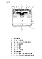
第1の実施形態に係る半導体装置の製造方法により製造された半導体装置について図1を参照して説明する。図1は、本発明の第1の実施形態に係る半導体装置の製造方法により製造された半導体装置の構成を示す断面図である。図1に示す第1の実施形態に係る半導体装置では、電界効果トランジスタの単位セルを2つ対向して並べた構造を備えている。なお、実際には、上記電界効果トランジスタの単位セルが複数並列に配置接続されて1つのトランジスタを形成している。
(First embodiment)
A semiconductor device manufactured by the method of manufacturing a semiconductor device according to the first embodiment will be described with reference to FIG. FIG. 1 is a cross-sectional view showing a configuration of a semiconductor device manufactured by the method for manufacturing a semiconductor device according to the first embodiment of the present invention. The semiconductor device according to the first embodiment shown in FIG. 1 has a structure in which two unit cells of a field effect transistor are arranged to face each other. In practice, a plurality of unit cells of the field effect transistor are arranged and connected in parallel to form one transistor.
図1に示す半導体装置は、半導体基体である基板領域1およびドリフト領域2を備えている。基板領域1は、炭化珪素のポリタイプが4HタイプのN+型(高濃度)の炭化珪素から形成されている。基板領域1の表面上に、N−型(低濃度)の炭化珪素からなるドリフト領域2が形成されている。
The semiconductor device shown in FIG. 1 includes a substrate region 1 and a
図1に示す半導体装置は、更に、電界効果トランジスタの各セルに対応して、ドリフト領域2と基板領域1との接合面の対向面、すなわち、ドリフト領域2の表面の所定領域に形成されたヘテロ半導体領域である第1のヘテロ半導体領域3と、ドリフト領域2と第1のヘテロ半導体領域3とのヘテロ接合部に接するように、ドリフト領域2の表面、第1のヘテロ半導体領域3の表面および側面に形成されたゲート絶縁膜4と、ゲート絶縁膜4に接して形成されたゲート電極5と、第1のヘテロ半導体領域3とドリフト領域2との接合面に対向する第1のヘテロ半導体領域3の表面と直接オーミック接続されたソース電極6と、基板領域1の裏面でオーミック接続されたドレイン電極7と、ソース電極5とゲート電極6を絶縁する層間絶縁膜8とを備えている。更に、第1のヘテロ半導体領域3とドリフト領域2とのヘテロ接合部の内、ゲート絶縁膜4と接する部分であるヘテロ接合駆動端部から所定距離離れ、かつ、ゲート絶縁膜4に接するドリフト領域2中に、第1の電界緩和領域であるP型のゲート電極下電界緩和領域9を備えている。ここで、第1の実施形態の第1のヘテロ半導体領域3は、ドリフト領域2と異なるバンドキャップ幅を有する半導体材料であるN型の多結晶シリコンを材料とし、ドリフト領域2とヘテロ接合している。そのため、ドリフト領域2と第1のヘテロ半導体領域3とのヘテロ接合界面にはエネルギー障壁ΔEcが存在している。また、ゲート絶縁膜4は、シリコン酸化膜から形成される。
The semiconductor device shown in FIG. 1 is further formed on a surface opposite to the junction surface between the
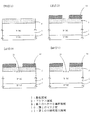
次に、第1の実施形態に係る半導体装置の製造方法について図2乃至図3を参照して説明する。図2乃至図3は、図1に示す半導体装置の第1の製造方法を示す断面図である。まず、図2(1)に示すように、N+型の基板領域1上にN−型のドリフト領域2をエピタキシャル成長させて、N型の炭化珪素半導体基体を形成する。次に、N型の炭化珪素半導体基体上に、例えばLP−CVD法で多結晶シリコン層を形成する。次に、多結晶シリコン層に、例えばイオン注入法でリンもしくはヒ素を不純物導入することで、N型の第1のヘテロ半導体領域3が形成される。次に、図2(2)に示すように、第1のヘテロ半導体領域3上に、例えばCVD酸化膜をフォトリソグラフィによって、所定形状に開口した第1のマスク材10を形成する。次に、図2(3)に示すように、第1のマスク材10で覆われていない部分において、第1のヘテロ半導体領域3を介してドリフト領域2中に、例えばイオン注入法を用いて、例えばボロンもしくはアルミなどを不純物導入し、第1の不純物導入領域11を形成する。
Next, a method for manufacturing the semiconductor device according to the first embodiment will be described with reference to FIGS. 2 to 3 are cross-sectional views showing a first method for manufacturing the semiconductor device shown in FIG. First, as shown in FIG. 2A, an N−
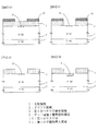
次に、図2(4)に示すように、さらに引き続き、第1のマスク材10で覆われていない部分において、第1のヘテロ半導体領域3を、例えば反応性イオンエッチング(ドライエッチング)によりエッチングする。次に、図3(5)に示すように、例えばフッ化アンモニウムとフッ酸との混合溶液で第1のマスク材10をウエットエッチングして除去する。次に、図3(6)に示すように、例えばドライO2酸化によって、第1のヘテロ半導体領域3の一部を所定の厚さ酸化すると同時に、第1の不純物導入領域11を活性化してゲート電極下電界緩和領域9を形成する。次に、例えばフッ化アンモニウムとフッ酸との混合溶液で、第1のヘテロ半導体領域3の酸化された部分をウエットエッチングして等方的に除去する。このように、共に第1のマスク材10を用いて、第1のヘテロ半導体領域3並びにゲート電極下電界緩和領域9を形成することで、全ての単位セルにおいて、それぞれ均一に所定距離離れるように形成する。
Next, as shown in FIG. 2 (4), the first
最後に、図3(7)に示すように、第1のヘテロ半導体領域3並びに露出したドリフト領域2上に、例えばLP−CVD法によってシリコン酸化膜からなるゲート絶縁膜4および、例えばLP−CVD法によって形成された多結晶シリコン層を堆積する。そして、多結晶シリコン層に、例えばイオン注入法でリンもしくはヒ素を不純物導入することで、N型のゲート電極5が形成される。そして、所定のマスク材で、ゲート電極5をパターニングし、ゲート絶縁膜4およびゲート電極5上に、例えばCVD法によって層間絶縁膜8を形成する。そして、ドリフト領域2と基板領域1との接合面の対向面、すなわち、基板領域1の裏面側に、例えば、チタン(Ti)、ニッケル(Ni)からなるドレイン電極7を形成する。順不同で、層間絶縁膜8、ゲート絶縁膜4および第1のヘテロ半導体領域3に接するように、例えばチタン(Ti)、アルミニウム(Al)からなるソース電極6を形成し、図1に示した本発明の第1の実施形態による半導体装置を完成させる。
Finally, as shown in FIG. 3B, on the first
以上のように、第1の実施形態に係る半導体装置では、ゲート電界が及ぶヘテロ接合駆動端部から所定距離に離れた所定部分に、漏れ電流を低減するゲート電極下電界緩和領域9をセルフアライメントで形成しているので、オン抵抗に優れ、かつ漏れ電流を低減できる。また、第1の製造方法では、ヘテロ接合駆動端部とゲート電極下電界緩和領域9とが、共に第1のマスク材10を用いて、かつ、厚み制御が容易な熱酸化法を用いて形成されるため、セルフアライメントで最適の距離に離して形成することができる。また、第1の実施形態に係る半導体装置の単位セルを複数有するデバイス構造とした場合も、ヘテロ接合駆動端部とゲート電極下電界緩和領域9との距離が全てのセルにおいて均一になるように形成することができ、高い信頼性を得ることができる。
As described above, in the semiconductor device according to the first embodiment, the electric
次に、第1の実施形態に係る半導体装置の動作について説明する。第1の実施形態に係る半導体装置では、ソース電極6を接地し、ドレイン電極7に正電位を印加して使用する。まず、ゲート電極5を例えば接地電位もしくは負電位とした場合、遮断状態を保持する。すなわち、第1のヘテロ半導体領域3とドリフト領域2とのヘテロ接合界面には、伝導電子に対するエネルギー障壁ΔEcが形成されているためである。上記遮断状態時、ヘテロ接合界面ではエネルギー障壁ΔEcの高さ並びにドレイン電界の大きさに応じて漏れ電流が生じる。第1の実施形態においては、ゲート電極下電界緩和領域9がヘテロ接合駆動端部よりも深い位置に形成されており、ゲート電極下電界緩和領域9とドリフト領域2の接合部にも逆バイアスが印加されるため、上記ゲート電極下電界緩和領域9とドリフト領域2の接合部から主にドリフト領域2側に空乏層が広がる。上記ゲート電極下電界緩和領域9から伸びた空乏層によって、ヘテロ接合駆動端部周辺のドレイン電界を緩和することができるため、上記漏れ電流を低減することができる。また、ゲート電極下電界緩和領域9の深さが深いほど、より高い漏れ電流低減効果を取得することができる。
Next, the operation of the semiconductor device according to the first embodiment will be described. In the semiconductor device according to the first embodiment, the
次に、遮断状態から導通状態へと転じるべく、ゲート電極5に正電位を印加した場合、ゲート絶縁膜4を介して、第1のヘテロ半導体領域3のヘテロ接合駆動端部並びにドリフト領域2の表層部にゲート電界が及び、上記ヘテロ接合駆動端部並びに上記表層部に、電子の蓄積層が形成される。すると、第1のヘテロ半導体領域3並びにドリフト領域2の表層部においては自由電子が存在可能なポテンシャルとなり、ドリフト領域2側に伸びていたエネルギー障壁ΔEcが急峻になり、エネルギー障壁ΔEcの厚みが小さくなる。その結果、電子電流が導通する。また、第1の実施形態では、遮断状態時に漏れ電流をより低減するために、ゲート電極下電界緩和領域9を形成しているが、導通状態においては、電流の導通特性を妨げないようにする必要がある。すなわち、ゲート電界が及ぶヘテロ接合駆動端部とゲート電極下電界緩和領域9が近すぎると導通時に所望の導通特性が得られず、遠すぎると遮断時の漏れ電流低減効果が低下するためである。そこで、第1の実施形態に係る半導体装置の製造方法を用いることで、遮断時の漏れ電流を大きく低減し、かつ、導通時の高い導通特性が得られる所定の位置に、ゲート電極下電界緩和領域9をセルフアライメントで、かつ、位置制御が容易に形成することができる。また、第1の実施形態に係る半導体装置の単位セルを複数有するデバイス構造とした場合も、ヘテロ接合駆動端部とゲート電極下電界緩和領域9との距離が全てのセルにおいて均一になるため、導通時の電流経路や遮断時の電界分布などが均一となることから、導通時、遮断時の面内バラつきが生じにくくなり、信頼性を含め、単位セルを複数有するデバイス素子自体の基本性能が向上する。
Next, when a positive potential is applied to the
次に、導通状態から遮断状態に移行すべく、再びゲート電極5を接地電位とすると、第1のヘテロ半導体領域3並びにドリフト領域2のヘテロ接合界面に形成されていた伝導電子の蓄積状態が解除され、エネルギー障壁ΔEc中のトンネリングが止まる。そして、第1のヘテロ半導体領域3からドリフト領域2への伝導電子の流れが止まり、さらにドリフト領域2中にあった伝導電子は基板領域1に流れ枯渇すると、ドリフト領域2側にはヘテロ接合部から空乏層が広がり遮断状態となる。また、ゲート電極下電界緩和領域9から伸びた空乏層によって、ヘテロ接合駆動端部周辺に広がっていたドレイン電界を緩和し、低い漏れ電流で遮断状態を維持する。
Next, when the
また、第1の実施形態においては、従来構造と同様に、例えばソース電極6を接地し、ドレイン電極7に負電位が印加された逆方向導通(還流動作)も可能である。上記の場合、ソース電極6並びにゲート電極5を接地電位とし、ドレイン電極7に所定の負電位が印加されると、伝導電子に対するエネルギー障壁ΔEcは消滅し、ドリフト領域2側から第1のヘテロ半導体領域3側に伝導電子が流れ、逆導通状態となる。上記逆導通状態時、正孔の注入はなく伝導電子のみで導通するため、逆導通状態から遮断状態に移行する際の逆回復電流による損失も小さい。なお、上述したゲート電極5を接地にせずに制御電極として使用する場合も可能である。
In the first embodiment, similarly to the conventional structure, for example, reverse conduction (reflux operation) in which the
(第2の実施形態)
次に、第2の実施形態に係る半導体装置の製造方法について、第1の実施形態に係る半導体装置の製造方法と異なる点を中心に図4を参照して説明する。また、第2の実施形態に係る半導体装置の製造方法により製造された半導体装置は、第1の実施形態に係る半導体装置と全く同じ構造を有している。図4は、本発明の第2の実施形態に係る半導体装置の製造方法を示す断面図である。第2の実施形態に係る半導体装置の製造方法では、第1の実施形態と異なり、第1のマスク材10で覆われていない第1のヘテロ半導体領域3の一部分をエッチングする工程を第1の不純物導入領域11を形成する工程より先に実施する場合を示している。具体的には、図2(2)に示した工程の後、図4(1)に示すように、第1のマスク材10で覆われていない部分において、第1のヘテロ半導体領域3を、例えば反応性イオンエッチング(ドライエッチング)によりエッチングする。次に、図4(2)では、第1のマスク材10で覆われていない部分において、ドリフト領域2中に、例えばイオン注入法を用いて、例えばボロンもしくはアルミなどを不純物導入し、第1の不純物導入領域11を形成する。最後に、第1の実施形態と同様に、図3(5)〜図3(7)の工程を実施し、図1に示した半導体装置と同じ構造の半導体装置を完成させる。これにより、第1のヘテロ半導体領域3と第1の不純物導入領域11の製造順序を逆にしても容易に製造することができる。また、第1の実施形態と同様の効果も取得できる。
(Second Embodiment)
Next, a method for manufacturing a semiconductor device according to the second embodiment will be described with reference to FIG. 4 focusing on differences from the method for manufacturing a semiconductor device according to the first embodiment. The semiconductor device manufactured by the method for manufacturing a semiconductor device according to the second embodiment has the same structure as the semiconductor device according to the first embodiment. FIG. 4 is a cross-sectional view showing a method of manufacturing a semiconductor device according to the second embodiment of the present invention. In the method for manufacturing a semiconductor device according to the second embodiment, unlike the first embodiment, the first step of etching a portion of the first
(第3の実施形態)
次に、第3の実施形態に係る半導体装置の製造方法について、第1の実施形態に係る半導体装置の製造方法と異なる点を中心に図5を参照して説明する。また、第3の実施形態に係る半導体装置の製造方法により製造された半導体装置は、第1の実施形態に係る半導体装置と全く同じ構造を有している。図5は、本発明の第3の実施形態に係る半導体装置の製造方法を示す断面図である。第3の実施形態に係る半導体装置の製造方法では、第1および第2の実施形態と異なり、第1のマスク材10で覆われていない第1のヘテロ半導体領域3の一部分をエッチングする工程で、第1のヘテロ半導体領域3を所定厚み残す場合を示している。具体的には、図2(3)に示した工程の後、図5(1)に示すように、第1のマスク材10で覆われていない部分において、第1のヘテロ半導体領域3を所定厚み残すように、例えば反応性イオンエッチング(ドライエッチング)によりエッチングする。次に、図5(2)では、例えばフッ化アンモニウムとフッ酸との混合溶液で第1のマスク材10をウエットエッチングして除去した後に、例えばドライO2酸化によって、第1のヘテロ半導体領域3の表面を酸化する。特に、図5(1)の工程で残したエッチング残し部分(底部)とエッチングサイド部が所定厚み酸化されるようにする。同時に、第1の不純物導入領域11を活性化し、ゲート電極下電界緩和領域9も形成する。次に、フッ化アンモニウムとフッ酸との混合溶液で、第1のヘテロ半導体領域3の酸化された部分をウエットエッチングして等方的に除去する。最後に、第1の実施形態と同様に、図3(7)の工程を実施し、図1に示した半導体装置と同じ構造の半導体装置を完成させる。これにより、第1のヘテロ半導体領域3の端部とゲート電極下電界緩和領域9が所定距離離れるように形成することができる。また、第1の実施形態と同様の効果も取得できる。更に、エッチング選択比の高いドライエッチとダメージ除去が可能な熱酸化とを組み合わせて、第1のヘテロ半導体領域3を所定厚み残してドライエッチングした後、上記の厚みを酸化することで、ドライエッチング時に生じるプラズマダメージがヘテロ接合駆動端部やドリフト領域2表面に生じなくなり、微細加工が可能となる。これにより、導通動作時において、ダメージによるゲート電界の終端が起こらず、高い導通特性を得ることができる。
(Third embodiment)
Next, a manufacturing method of the semiconductor device according to the third embodiment will be described with reference to FIG. 5 focusing on differences from the manufacturing method of the semiconductor device according to the first embodiment. A semiconductor device manufactured by the method for manufacturing a semiconductor device according to the third embodiment has the same structure as the semiconductor device according to the first embodiment. FIG. 5 is a sectional view showing a method for manufacturing a semiconductor device according to the third embodiment of the present invention. In the method of manufacturing a semiconductor device according to the third embodiment, unlike the first and second embodiments, a step of etching a part of the first
(第4の実施形態)
次に、第4の実施形態に係る半導体装置の製造方法について、第1の実施形態に係る半導体装置の製造方法と異なる点を中心に図6を参照して説明する。また、第4の実施形態に係る半導体装置の製造方法により製造された半導体装置は、第1の実施形態に係る半導体装置と全く同じ構造を有している。図6は、本発明の第4の実施形態に係る半導体装置の製造方法を示す断面図である。第4の実施形態では、第1乃至第3の実施形態と異なり、第1のマスク材10の開口部を広げた後、ヘテロ接合駆動端部を形成する場合を示している。具体的には、図2(3)に示した工程の後、図6(1)に示すように、例えばフッ化アンモニウムとフッ酸との混合溶液で第1のマスク材10を所定厚みだけ等方的にウエットエッチングして開口部を広げる。次に、図6(2)では、第1のマスク材10で覆われていない第1のヘテロ半導体領域3の一部分を、例えば反応性イオンエッチング(ドライエッチング)によりエッチングする。次に、図6(3)では、例えばフッ化アンモニウムとフッ酸との混合溶液で第1のマスク材10をウエットエッチングして除去する。次に、図6(4)では、所定の熱処理によって、第1の不純物導入領域11を活性化し、ゲート電極下電界緩和領域9を形成する。最後に、第1の実施形態と同様に、図3(7)の工程を実施し、図1に示した半導体装置と同じ構造の半導体装置を完成させる。これにより、第1乃至第3の実施形態で示した第1のヘテロ半導体領域3の犠牲酸化を用いずとも、容易にヘテロ接合駆動端部とゲート電極下電界緩和領域9が所定距離離れるように形成することができる。また、第1の実施形態と同様の効果も取得できる。
(Fourth embodiment)
Next, a manufacturing method of the semiconductor device according to the fourth embodiment will be described with reference to FIG. 6 focusing on differences from the manufacturing method of the semiconductor device according to the first embodiment. A semiconductor device manufactured by the method for manufacturing a semiconductor device according to the fourth embodiment has the same structure as the semiconductor device according to the first embodiment. FIG. 6 is a sectional view showing a method for manufacturing a semiconductor device according to the fourth embodiment of the present invention. In the fourth embodiment, unlike the first to third embodiments, the case where the heterojunction driving end is formed after the opening of the
(第5の実施形態)
次に、第5の実施形態に係る半導体装置の製造方法について、第1の実施形態と異なる点を中心に図7乃至図9を参照して説明する。また、第5の実施形態に係る半導体装置の製造方法により製造された半導体装置について、第1の実施形態に係る半導体装置と同様の構造には同じ番号を付し、説明を省略する。
(Fifth embodiment)
Next, a method for manufacturing a semiconductor device according to the fifth embodiment will be described with reference to FIGS. 7 to 9 focusing on differences from the first embodiment. Also, in the semiconductor device manufactured by the method for manufacturing a semiconductor device according to the fifth embodiment, the same structure as that of the semiconductor device according to the first embodiment is denoted by the same reference numeral, and description thereof is omitted.
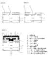
まず、第5の実施形態に係る半導体装置の製造方法により製造された半導体装置について図7を参照して説明する。図7は、本発明の第5の実施形態に係る半導体装置の製造方法により製造された半導体装置の構成を示す断面図である。図7に示すように、第5の実施形態に係る半導体装置の構造は、第1の実施形態の半導体装置の構造と基本的には同じである。第5の実施形態の半導体装置が、第1の実施形態と異なる点は、ヘテロ接合駆動端部から所定距離はなれ、かつ第1のヘテロ半導体領域3に接するように、ドリフト領域2中に第2の電界緩和領域であるソース領域下電界緩和領域12が形成されている点だけである。これにより、第1の実施形態と同様に、ゲート電界が及ぶヘテロ接合駆動端部から所定距離に離れた所定部分に、漏れ電流を低減するゲート電極下電界緩和領域9をセルフアライメントで形成しているので、オン抵抗に優れ、かつ漏れ電流を低減できる。また、ソース領域下電界緩和領域12の形成によって、第1のヘテロ半導体領域3とドリフト領域2とが接するヘテロ接合面の面積が小さくなるため、遮断状態時に上記ヘテロ接合面で生じる漏れ電流を、第1の実施形態に係る半導体装置よりも低減することができる。
First, a semiconductor device manufactured by the method for manufacturing a semiconductor device according to the fifth embodiment will be described with reference to FIG. FIG. 7 is a cross-sectional view showing a configuration of a semiconductor device manufactured by the method for manufacturing a semiconductor device according to the fifth embodiment of the present invention. As shown in FIG. 7, the structure of the semiconductor device according to the fifth embodiment is basically the same as the structure of the semiconductor device of the first embodiment. The semiconductor device of the fifth embodiment is different from the first embodiment in that a second distance is included in the
次に、第5の実施形態に係る半導体装置の製造方法について、図8および図9を参照して説明する。図8乃至図9は、図7に示す半導体装置の製造方法を示す断面図である。まず、図8(1)においては、第1の実施形態の図2(1)に示した工程の後、第1のヘテロ半導体領域3上に、例えばCVD酸化膜をフォトリソグラフィによって所定形状に開口した第1のマスク材10を形成する。次に、図8(2)に示すように、第1のマスク材10で覆われていない部分において、第1のヘテロ半導体領域3を介してドリフト領域2中に、例えばイオン注入法を用いて、例えばボロンもしくはアルミなどを不純物導入し、第1の不純物導入領域11並びに第2の不純物導入領域13を形成する。次に、図8(3)に示すように、第1のマスク材10で覆われていない部分の内、所定部分、すなわち、第2の不純物導入領域13(ソース領域下電界緩和領域12)と接する第1のヘテロ半導体領域3の部分を覆うように、例えばレジストマスクからなる第2のマスク材14を形成する。第5の実施形態では、第2のマスク材14を第1のマスク材10と異なる材料を用いて形成しているので、容易にパターニングすることができる。しかしながら、第2のマスク材14と第1のマスク材10を同一の材料を用いて形成する場合にも、厚みや熱処理などの履歴を変えることで、図8(3)の構造を形成することも可能である。
Next, a method for manufacturing a semiconductor device according to the fifth embodiment will be described with reference to FIGS. 8 to 9 are cross-sectional views showing a method for manufacturing the semiconductor device shown in FIG. First, in FIG. 8A, after the step shown in FIG. 2A of the first embodiment, for example, a CVD oxide film is opened in a predetermined shape on the first
次に、図8(4)に示すように、第1のマスク材10および第2のマスク材14のどちらにも覆われていない第1のヘテロ半導体領域3の剥き出し部分を、例えば反応性イオンエッチング(ドライエッチング)によりエッチングする。次に、図9(5)に示すように、例えば硫酸と過酸化水素水の混合溶液で第2のマスク材14を除去した後、例えばフッ化アンモニウムとフッ酸との混合溶液で第1のマスク材10をウエットエッチングして除去する。次に、図9(6)に示すように、例えばドライO2酸化によって、第1のヘテロ半導体領域3の一部を所定の厚さ酸化すると同時に、第1の不純物導入領域11並びに第2の不純物導入領域13を活性化し、ゲート電極下電界緩和領域9並びにソース領域下電界緩和領域12を形成する。第5の実施形態では、ゲート電極下電界緩和領域9の深さとソース領域下電界緩和領域12の深さは同じにしている。次に、フッ化アンモニウムとフッ酸との混合溶液で、第1のヘテロ半導体領域3の酸化された部分をウエットエッチングして等方的に除去する。最後に、図9(7)に示すように、第1のヘテロ半導体領域3並びに露出したドリフト領域2上に、例えばLP−CVD法によってシリコン酸化膜からなるゲート絶縁膜4および、例えばLP−CVD法によって形成された多結晶シリコン層を堆積する。そして、多結晶シリコン層に、例えばイオン注入法でリンもしくはヒ素を不純物導入することで、N型のゲート電極5が形成される。そして、所定のマスク材で、ゲート電極5をパターニングし、ゲート絶縁膜4およびゲート電極5上に例えばCVD法によって層間絶縁膜8を形成する。そして、基板領域1の裏面側に、例えば、チタン(Ti)、ニッケル(Ni)からなるドレイン電極7を形成する。順不同で、層間絶縁膜8、ゲート絶縁膜4および第1のヘテロ半導体領域3に接するように、例えばチタン(Ti)、アルミニウム(Al)からなるソース電極6を形成し、図7に示した本発明の第5の実施形態による半導体装置を完成させる。
Next, as shown in FIG. 8 (4), the exposed portion of the first
以上のように、第5の実施形態に係る半導体装置の製造方法では、ヘテロ接合駆動端部、ゲート電極下電界緩和領域9並びにソース領域下電界緩和領域12が、共に第1のマスク材10を用いて、かつ、厚み制御が容易な熱酸化法を用いて形成されるため、セルフアライメントで最適の距離に離して形成することができる。そのため、第5の実施形態に係る半導体装置の単位セルを複数有するデバイス構造とした場合も、ヘテロ接合駆動端部とゲート電極下電界緩和領域9並びにソース領域下電界緩和領域12との距離が全てのセルにおいて均一になるように形成することができる。よって、導通時の電流経路や遮断時の電界分布などが均一となることから、導通時、遮断時の面内バラつきが生じにくくなり、信頼性を含め、上記単位セルを複数有するデバイス素子自体の基本性能が向上する。
As described above, in the method of manufacturing a semiconductor device according to the fifth embodiment, the heterojunction driving end, the electric
(第6の実施形態)
次に、第6の実施形態に係る半導体装置の製造方法について、第5の実施形態に係る半導体装置の製造方法と異なる点を中心に図10乃至図11を参照して説明する。また、第6の実施形態に係る半導体装置の製造方法により製造された半導体装置について、第5の実施形態に係る半導体装置と同様の構造には同じ番号を付し、説明を省略する。
(Sixth embodiment)
Next, a semiconductor device manufacturing method according to the sixth embodiment will be described with reference to FIGS. 10 to 11 focusing on differences from the semiconductor device manufacturing method according to the fifth embodiment. Also, in the semiconductor device manufactured by the method for manufacturing a semiconductor device according to the sixth embodiment, the same structure as that of the semiconductor device according to the fifth embodiment is denoted by the same reference numeral, and description thereof is omitted.
まず、第6の実施形態に係る半導体装置の製造方法により製造された半導体装置について図10を参照して説明する。図10は、本発明の第6の実施形態に係る半導体装置の製造方法により製造された半導体装置の構成を示す断面図である。図10に示すように、第6の実施形態に係る半導体装置の構造は、第5の実施形態の半導体装置の構造と基本的には同じである。第6の実施形態の半導体装置が、第5の実施形態と異なる点は、ゲート電極下電界緩和領域9の深さを、ソース領域下電界緩和領域12の深さより深くしている点だけである。これにより、第5の実施形態と同様の効果を取得できる。更に、ゲート電極下電界緩和領域9とソース領域下電界緩和領域12の深さを違えることで、導通時の駆動性能と遮断時の漏れ電流低減との両立を容易に設計することが可能になる。
First, a semiconductor device manufactured by the method for manufacturing a semiconductor device according to the sixth embodiment will be described with reference to FIG. FIG. 10 is a cross-sectional view showing a configuration of a semiconductor device manufactured by the method for manufacturing a semiconductor device according to the sixth embodiment of the present invention. As shown in FIG. 10, the structure of the semiconductor device according to the sixth embodiment is basically the same as the structure of the semiconductor device according to the fifth embodiment. The semiconductor device of the sixth embodiment is different from the fifth embodiment only in that the depth of the electric
次に、第6の実施形態に係る半導体装置の製造方法について、図11を参照して説明する。図11は、図10に示す半導体装置の製造方法を示す断面図である。まず、図11(1)において、第5の実施形態の図8(3)に示した工程の後、第1のマスク材10並びに第2のマスク材14で覆われていない部分において、第1のヘテロ半導体領域3を介して第1の不純物導入領域11より深い領域で、かつドリフト領域2中に、例えばイオン注入法を用いて、例えばボロンもしくはアルミなどを不純物導入し、第3の不純物導入領域15を追加して形成する。次に、図11(2)に示すように、第1のマスク材10および第2のマスク材14のどちらにも覆われていない第1のヘテロ半導体領域3の剥き出し部分を、例えば反応性イオンエッチング(ドライエッチング)によりエッチングする。次に、例えば硫酸と過酸化水素水の混合溶液で第2のマスク材14を除去した後、例えばフッ化アンモニウムとフッ酸との混合溶液で第1のマスク材10をウエットエッチングして除去する。
Next, a method for manufacturing a semiconductor device according to the sixth embodiment will be described with reference to FIG. FIG. 11 is a cross-sectional view showing a method of manufacturing the semiconductor device shown in FIG. First, in FIG. 11 (1), after the step shown in FIG. 8 (3) of the fifth embodiment, the
次に、図11(3)に示すように、例えばドライO2酸化によって、第1のヘテロ半導体領域3の一部を所定の厚さ酸化すると同時に、第1の不純物導入領域11、第3の不純物導入領域15並びに第2の不純物導入領域13を活性化し、ゲート電極下電界緩和領域9並びにソース領域下電界緩和領域12を形成する。第6の実施形態では、第3の不純物導入領域15を形成しているので、ゲート電極下電界緩和領域9の深さは、ソース領域下電界緩和領域12の深さより深くなる。次に、フッ化アンモニウムとフッ酸との混合溶液で、第1のヘテロ半導体領域3の酸化された部分をウエットエッチングして等方的に除去する。最後に、第5の実施形態と同様に、図9(7)の工程を実施し、図10に示した本発明の第6の実施形態による半導体装置を完成させる。上記のようにすることで、第1のヘテロ半導体領域3の端部とゲート電極下電界緩和領域9並びにソース領域下電界緩和領域12が所定距離離れ、かつゲート電極下電界緩和領域9がソース領域下電界緩和領域12より深くなるように形成することができる。
Next, as shown in FIG. 11 (3), a part of the first
(第7の実施形態)
次に、第7の実施形態に係る半導体装置の製造方法について、第5の実施形態と異なる点を中心に図12乃至図14を参照して説明する。また、第7の実施形態に係る半導体装置の製造方法により製造された半導体装置について、第5の実施形態に係る半導体装置と同様の構造には同じ番号を付し、説明を省略する。
(Seventh embodiment)
Next, a method for manufacturing a semiconductor device according to the seventh embodiment will be described with reference to FIGS. 12 to 14 focusing on differences from the fifth embodiment. Also, in the semiconductor device manufactured by the semiconductor device manufacturing method according to the seventh embodiment, the same reference numerals are given to the same structures as those of the semiconductor device according to the fifth embodiment, and description thereof is omitted.
まず、第7の実施形態に係る半導体装置の製造方法により製造された半導体装置について図12を参照して説明する。図12は、本発明の第7の実施形態に係る半導体装置の製造方法により製造された半導体装置の構成を示す断面図である。図12に示すように、第7の実施形態に係る半導体装置の構造は、第5の実施形態の半導体装置の構造と基本的には同じである。第7の実施形態の半導体装置が、第5の実施形態と異なる点は、ゲート電極下電界緩和領域9が形成されていない点だけである。これにより、ゲート電極5下にゲート電極下電界緩和領域9が形成されていないため、ゲート電極5の幅をより小さく形成することができる。よって、半導体装置の集積化が可能となる。
First, a semiconductor device manufactured by the method for manufacturing a semiconductor device according to the seventh embodiment will be described with reference to FIG. FIG. 12 is a cross-sectional view showing a configuration of a semiconductor device manufactured by the method for manufacturing a semiconductor device according to the seventh embodiment of the present invention. As shown in FIG. 12, the structure of the semiconductor device according to the seventh embodiment is basically the same as the structure of the semiconductor device according to the fifth embodiment. The semiconductor device of the seventh embodiment is different from the fifth embodiment only in that the electric
次に、第7の実施形態に係る半導体装置の製造方法について、図13および図14を参照して説明する。図13乃至図14は、図12に示す半導体装置の製造方法を示す断面図である。まず、図13(1)においては、第5の実施形態の図8(1)に示した工程の後、第1のヘテロ半導体領域3上に、第1のマスク材10で覆われていない部分の内、所定部分、すなわち、ソース領域下電界緩和領域12と接しない第1のへテロ半導体領域3の部分を、第1のマスク材10とともに覆うように、例えばレジストマスクからなる第3のマスク材16を形成する。第7の実施形態では、第3のマスク材16は第1のマスク材10と異なる材料を用いて形成しているので、容易にパターニングすることができる。しかしながら、第3のマスク材16と第1のマスク材10を同一の材料を用いて形成する場合にも、厚みや熱処理などの履歴を変えることによって、図13(1)の構造を形成することも可能である。次に、図13(2)に示すように、第1のマスク材10および第3のマスク材16のどちらにも覆われていない第1のヘテロ半導体領域3の剥き出し部分を通してドリフト領域2中に、例えばイオン注入法を用いて、例えばボロンもしくはアルミなどを不純物導入し、第2の不純物導入領域13を形成する。次に、図13(3)に示すように、第3のマスク材16を例えば硫酸と過酸化水素水の混合溶液で除去する。次に、第1のマスク材10で覆われていない部分の内、所定部分、すなわち、第2の不純物導入領域13(ソース領域下電界緩和領域12)と接する第1のヘテロ半導体領域3の部分を覆うように、例えばレジストマスクから成る第2のマスク材14を形成する。第2のマスク材14は第1のマスク材10と異なる材料を用いることで、容易にパターニングすることができる。しかしながら、第2のマスク材14と第1のマスク材10を同一の材料を用いて形成する場合にも、厚みや熱処理などの履歴を変えることによって、図13(3)の構造を形成することも可能である。
Next, a method for manufacturing a semiconductor device according to the seventh embodiment will be described with reference to FIGS. 13 to 14 are sectional views showing a method for manufacturing the semiconductor device shown in FIG. First, in FIG. 13A, after the step shown in FIG. 8A of the fifth embodiment, a portion not covered with the
次に、図13(4)に示すように、第1のマスク材10および第2のマスク材14のどちらにも覆われていない第1のヘテロ半導体領域3の剥き出し部分を、例えば反応性イオンエッチング(ドライエッチング)によりエッチングする。次に、図14(5)に示すように、例えば硫酸と過酸化水素水の混合溶液で第2のマスク材14を除去した後、例えばフッ化アンモニウムとフッ酸との混合溶液で第1のマスク材10をウエットエッチングして除去する。次に、図14(6)に示すように、例えばドライO2酸化によって、第1のヘテロ半導体領域3の一部を所定の厚さ酸化すると同時に、第2の不純物導入領域13を活性化し、ソース領域下電界緩和領域12を形成する。次に、フッ化アンモニウムとフッ酸との混合溶液で、第1のヘテロ半導体領域3の酸化された部分をウエットエッチングして等方的に除去する。
Next, as shown in FIG. 13 (4), the exposed portion of the first
最後に、図14(7)に示すように、第1のヘテロ半導体領域3並びに剥き出しになったドリフト領域2上に、例えばLP−CVD法によってシリコン酸化膜からなるゲート絶縁膜4および、例えばLP−CVD法によって形成された多結晶シリコン層を堆積する。そして、例えばイオン注入法でリンもしくはヒ素を不純物導入することで、N型のゲート電極5が形成される。そして、所定のマスク材で、ゲート電極5をパターニングし、ゲート絶縁膜4およびゲート電極5上に例えばCVD法によって層間絶縁膜8を形成する。そして、基板領域1の裏面側に、例えば、チタン(Ti)、ニッケル(Ni)からなるドレイン電極7を形成する。順不同で、層間絶縁膜8、ゲート絶縁膜4および第1のヘテロ半導体領域3に接するように、例えばチタン(Ti)、アルミニウム(Al)からなるソース電極6を形成し、図12に示した本発明の第7の実施形態による半導体装置を完成させる。
Finally, as shown in FIG. 14 (7), on the first
以上のように、第7の実施形態に係る半導体装置の製造方法では、第5および第6の実施形態と同様に、ヘテロ接合駆動端部とソース領域下電界緩和領域12とが、共に第1のマスク材10を用いて、かつ、厚み制御が容易な熱酸化法を用いて形成されるため、セルフアライメントで最適の距離に離して形成することができる。そのため、第7の実施形態に係る半導体装置の単位セルを複数有するデバイス構造とした場合も、ヘテロ接合駆動端部とソース領域下電界緩和領域12との距離が全てのセルにおいて均一になるように形成することができる。よって、導通時の電流経路や遮断時の電界分布などが均一となることから、導通時、遮断時の面内バラつきが生じにくくなり、信頼性を含め、上記単位セルを複数有するデバイス素子自体の基本性能が向上する。
As described above, in the method of manufacturing the semiconductor device according to the seventh embodiment, the heterojunction drive end and the source region lower electric
(第8の実施形態)
次に、第8の実施形態に係る半導体装置の製造方法について、第5の実施形態と異なる点を中心に図15乃至図16を参照して説明する。また、第8の実施形態に係る半導体装置の製造方法により製造された半導体装置について、第5の実施形態に係る半導体装置と同様の構造には同じ番号を付し、説明を省略する。
(Eighth embodiment)
Next, a method for manufacturing a semiconductor device according to the eighth embodiment will be described with reference to FIGS. 15 to 16 focusing on differences from the fifth embodiment. Also, in the semiconductor device manufactured by the method for manufacturing a semiconductor device according to the eighth embodiment, the same structure as that of the semiconductor device according to the fifth embodiment is denoted by the same reference numeral, and description thereof is omitted.
まず、第8の実施形態に係る半導体装置の製造方法により製造された半導体装置について図15を参照して説明する。図15は、本発明の第8の実施形態に係る半導体装置の製造方法により製造された半導体装置の構成を示す断面図である。図15に示すように、第8の実施形態に係る半導体装置の構造は、第5の実施形態の半導体装置の構造と基本的には同じである。第8の実施形態の半導体装置が、第5の実施形態と異なる点は、ゲート電極下電界緩和領域9の深さをソース領域下電界緩和領域12の深さよりも浅くしている点だけである。これにより、第5の実施形態と同様の効果を取得することができる。
First, a semiconductor device manufactured by the semiconductor device manufacturing method according to the eighth embodiment will be described with reference to FIG. FIG. 15 is a cross-sectional view showing a configuration of a semiconductor device manufactured by the method for manufacturing a semiconductor device according to the eighth embodiment of the present invention. As shown in FIG. 15, the structure of the semiconductor device according to the eighth embodiment is basically the same as the structure of the semiconductor device of the fifth embodiment. The semiconductor device of the eighth embodiment is different from the fifth embodiment only in that the depth of the electric
次に、第8の実施形態に係る半導体装置の製造方法について、図16を参照して説明する。図16は、図15に示す半導体装置の製造方法を示す断面図である。まず、図16(1)においては、第5の実施形態の図8(1)に示した工程の後、第1のヘテロ半導体領域3上に、第1のマスク材10で覆われていない部分の内、所定部分、すなわち、ソース領域下電界緩和領域12と接しない第1のへテロ半導体領域3の部分を、第1のマスク材10とともに覆うように、例えばレジストマスクからなる第3のマスク材16を形成する。第8の実施形態では、第3のマスク材16は第1のマスク材10と異なる材料を用いて形成しているので、容易にパターニングすることができる。しかしながら、第3のマスク材16と第1のマスク材10を同一の材料を用いて形成する場合にも、厚みや熱処理などの履歴を変えることによって、図16(1)の構造を形成することも可能である。次に、第1のマスク材10および第3のマスク材16のどちらにも覆われていない第1のヘテロ半導体領域3の剥き出し部分を通してドリフト領域2中に、例えばイオン注入法を用いて、例えばボロンもしくはアルミなどを不純物導入し、第2の不純物導入領域13を形成する。次に、図16(2)に示すように、第3のマスク材16を例えば硫酸と過酸化水素水の混合溶液で除去する。次に、第1のマスク材10で覆われていない部分の内、所定部分、すなわち、第2の不純物導入領域13(ソース領域下電界緩和領域12)と接する第1のヘテロ半導体領域3の部分を覆うように、例えばレジストマスクから成る第2のマスク材14を形成する。第2のマスク材14は第1のマスク材10と異なる材料を用いることで、容易にパターニングすることができる。しかしながら、第2のマスク材14と第1のマスク材10を同一の材料を用いて形成する場合にも、厚みや熱処理などの履歴を変えることによって、図16(2)の構造を形成することも可能である。
Next, a method for manufacturing a semiconductor device according to the eighth embodiment will be described with reference to FIG. 16 is a cross-sectional view showing a method of manufacturing the semiconductor device shown in FIG. First, in FIG. 16A, after the step shown in FIG. 8A of the fifth embodiment, a portion not covered with the
次に、第1のマスク材10および第2のマスク材14のどちらにも覆われていない第1のヘテロ半導体領域3の剥き出し部分を通して、例えばイオン注入法を用いてドリフト領域2中に、例えばボロンもしくはアルミなどを不純物導入し、第1の不純物導入領域11を形成する。なお、第8の実施形態では、第1の不純物導入領域11よりも深い領域に第3の不純物導入領域13を形成している。次に、図16(3)に示すように、第1のマスク材10および第2のマスク材14のどちらにも覆われていない第1のヘテロ半導体領域3の剥き出し部分を、例えば反応性イオンエッチング(ドライエッチング)によりエッチングする。次に、例えば硫酸と過酸化水素水の混合溶液で第2のマスク材14を除去した後、例えばフッ化アンモニウムとフッ酸との混合溶液で第1のマスク材10をウエットエッチングして除去する。次に、例えばドライO2酸化によって、第1のヘテロ半導体領域3の一部を所定の厚さ酸化すると同時に、第1の不純物導入領域11と第2の不純物導入領域13を活性化し、ゲート電極下電界緩和領域9とソース領域下電界緩和領域12を形成する。次に、フッ化アンモニウムとフッ酸との混合溶液で、第1のヘテロ半導体領域3の酸化された部分をウエットエッチングして等方的に除去する。
Next, through the exposed portion of the first
最後に、第5の実施形態と同様に、図9(7)の工程を実施し、図15に示した本発明の第8の実施形態による半導体装置を完成させる。これにより、第8の実施形態に係る半導体装置の製造方法では、ソース領域下電界緩和領域12よりも浅いゲート電極下電界緩和領域9をセルフアライメントで形成することもできる。また、第5の実施形態と同様の効果も取得できる。
Finally, similarly to the fifth embodiment, the process of FIG. 9B is performed to complete the semiconductor device according to the eighth embodiment of the present invention shown in FIG. As a result, in the method for manufacturing a semiconductor device according to the eighth embodiment, the electric
なお、以上に述べた実施形態は、本発明の実施の一例であり、本発明の範囲はこれらに限定されるものでなく、特許請求の範囲に記載した範囲内で、他の様々な実施形態に適用可能である。例えば、第1乃至第8の実施形態に係る半導体装置においては、本発明の特徴をわかりやすく説明するために、基本的な構造を具備したトランジスタ構造で説明したが、特にこれに限定されるものでなく、少なくとも、ヘテロ接合駆動端部と、ソース領域下電界緩和領域12もしくはゲート電極下電界緩和領域9のいずれか一方もしくは両方とが、所定距離離れるように、第1のマスク材10を用いてセルフアライメントで形成する本発明と同様の製造方法により製造される半導体装置であれば、当該半導体装置にどのような構造が付加されていても良い。また、どのように変形されていても良い。
The embodiment described above is an example of the implementation of the present invention, and the scope of the present invention is not limited thereto, and other various embodiments are within the scope described in the claims. It is applicable to. For example, in the semiconductor devices according to the first to eighth embodiments, the transistor structure having the basic structure has been described for easy understanding of the features of the present invention, but the present invention is particularly limited to this. Instead, the
具体的には、図17乃至図19に示す第1の実施形態に係る半導体装置、第5の実施形態に係る半導体装置および第7の実施形態に係る半導体装置を利用した半導体装置でも良い。ここで、図17乃至図19は、各実施形態に係る半導体装置のドリフト領域2に形成された溝に接するように、ゲート絶縁膜4を介してゲート電極5が形成された半導体装置を示している。これから、図17乃至図19に示す半導体装置は、各実施形態に係る半導体装置と同様の効果を取得できる。また、図17乃至図19に示す半導体装置は、第4の実施形態で説明したように、第1のマスク材10を等方性のエッチングによって開口部を広げた後に、第1のヘテロ半導体領域3とドリフト領域2の表層部をドライエッチングすることによって、容易に製造することもできる。
Specifically, the semiconductor device according to the first embodiment shown in FIGS. 17 to 19, the semiconductor device according to the fifth embodiment, and the semiconductor device using the semiconductor device according to the seventh embodiment may be used. Here, FIG. 17 to FIG. 19 show the semiconductor device in which the
更に、図20乃至図22に示す第1の実施形態に係る半導体装置、第5の実施形態に係る半導体装置および第7の実施形態に係る半導体装置を利用した半導体装置でも良い。ここで、図20乃至図22は、各実施形態に係る半導体装置のドリフト領域2に形成された溝とヘテロ接合駆動端部が所定距離離れており、溝ならびにヘテロ接合駆動端部に接するように、ゲート絶縁膜4を介してゲート電極5が形成された半導体装置を示している。これから、図20乃至図22に示す半導体装置は、各実施形態に係る半導体装置と同様の効果を取得できる。また、図20乃至図22に示す半導体装置は、例えば図3(5)の工程において、第1のヘテロ半導体領域3だけでなくドリフト領域2の表層部をドライエッチングして、ドライエッチング後、犠牲酸化によって第1のヘテロ半導体領域3の端部が後退することで、容易に製造することができる。
Furthermore, the semiconductor device according to the first embodiment shown in FIGS. 20 to 22, the semiconductor device according to the fifth embodiment, and the semiconductor device using the semiconductor device according to the seventh embodiment may be used. Here, in FIG. 20 to FIG. 22, the groove formed in the
更に、図23乃至図25に示す第1の実施形態に係る半導体装置、第5の実施形態に係る半導体装置および第7の実施形態に係る半導体装置を利用した半導体装置でも良い。ここで、図23乃至図25は、各実施形態に係る半導体装置の第1のヘテロ半導体領域3中に不純物の導電型および不純物濃度のいずれか一方もしくは両方が異なる領域から形成され、ソース電極6とオーミックコンタクする、例えばN+型の第2のヘテロ半導体領域17を有する半導体装置を示している。これから、図23乃至図25に示す半導体装置は、各実施形態に係る半導体装置と同様の効果を取得できる。なお、図23乃至図25に示す半導体装置においては、第2のヘテロ半導体領域17を、第1のヘテロ半導体領域3が形成された時点で、所定の不純物を導入して形成しても良い。また、ゲート電極5をパターニングした後に不純物を導入して形成しても良い。これから、第2のヘテロ半導体領域17を容易に形成することができる。更に、図23乃至図25に示す半導体装置では、所定深さで所定位置に第2のヘテロ半導体領域17を形成しているが、第2のヘテロ半導体領域17を層状に形成しても良い。また、ライン状などローカルに形成しても良い。
Furthermore, the semiconductor device according to the first embodiment shown in FIGS. 23 to 25, the semiconductor device according to the fifth embodiment, and the semiconductor device using the semiconductor device according to the seventh embodiment may be used. Here, FIG. 23 to FIG. 25 are formed in the first
更に、図26乃至図28に示す第1の実施形態に係る半導体装置、第5の実施形態に係る半導体装置および第7の実施形態に係る半導体装置を利用した半導体装置でも良い。ここで、図26乃至図28は、各実施形態に係る半導体装置のヘテロ接合駆動端部に接するように、ドリフト領域2中に例えばN+型の導通領域18が形成された半導体装置を示している。これより、導通時、より低い抵抗で電流を流すことができる。また、導通領域18は第1のヘテロ半導体領域3の端部を犠牲酸化によって後退させた後に形成することができる。これから、容易に製造することができる。
Furthermore, the semiconductor device according to the first embodiment shown in FIGS. 26 to 28, the semiconductor device according to the fifth embodiment, and the semiconductor device using the semiconductor device according to the seventh embodiment may be used. Here, FIG. 26 to FIG. 28 show a semiconductor device in which, for example, an N +
また、全ての実施形態の半導体装置、すなわち、第1乃至第8の実施形態に係る半導体装置および図17乃至図28に示した各実施形態を利用した半導体装置では、第1のヘテロ半導体領域3の側壁は全て垂直形状としているが、特にこれに限定されるものでなく、傾斜を持っていても良い。更に、全ての実施形態の半導体装置において、炭化珪素からなる半導体基体を有する半導体装置について説明したが、特にこれに限定されるものでなく、半導体基体の基板材料は窒化ガリウム、ダイヤモンドなどその他の半導体材料でもかまわない。また、全ての実施形態の半導体装置において、炭化珪素のポリタイプが4Hタイプの炭化珪素から形成された基板領域1について説明したが、特にこれに限定されるものでなく、6H、3C等その他のポリタイプで形成された基板領域を用いることもできる。また、全ての実施形態の半導体装置を、ドレイン電極7とソース電極6とをドリフト領域2を挟んで対向するように配置し、電流を縦方向に流す所謂縦型構造のトランジスタで説明してきたが、特にこれに限定されるものでなく、例えばドレイン電極7とソース電極6とを同一主面上に配置し、電流を横方向に流す所謂横型構造のトランジスタであってもかまわない。
In the semiconductor devices of all the embodiments, that is, the semiconductor devices according to the first to eighth embodiments and the semiconductor devices using the embodiments shown in FIGS. 17 to 28, the first
また、全ての実施形態の半導体装置において、第1のヘテロ半導体領域3の材料として多結晶シリコンを用いているが、特にこれに限定されるものでなく、炭化珪素とヘテロ接合を形成する材料であれば、例えば単結晶シリコン、アモルファスシリコン等その他のシリコン材料、ゲルマニウムやシリコンゲルマン等その他の半導体材料または6H、3C等炭化珪素の他のポリタイプなど、どの材料でもかまわない。また、全ての実施形態の半導体装置では、N型の炭化珪素からなるドリフト領域2とN型の多結晶シリコンを材料とする第1のヘテロ半導体領域3とからなるヘテロ接合部を有する半導体装置について説明しているが、特にこれに限定されるものでなく、それぞれN型の炭化珪素とP型の多結晶シリコン、P型の炭化珪素とP型の多結晶シリコン、P型の炭化珪素とN型の多結晶シリコンの如何なる組み合わせでも良い。更に、全ての実施形態の半導体装置では、基板領域1とゲート電極5の導電型もN型としているが、特にこれに限定されるものでなく、P型としても良い。
Moreover, in the semiconductor devices of all the embodiments, polycrystalline silicon is used as the material of the first
また、全ての実施形態の半導体装置では、第1のマスク材10の材料としてCVD酸化膜を用いているが、特にこれに限定されるものでなく、フォトレジスト膜やSiN膜など別の材料を用いていても良い。
Further, in all the semiconductor devices of the embodiments, the CVD oxide film is used as the material of the
また、全ての実施形態の半導体装置の層間絶縁膜8の材料として、例えばシリコン酸化膜やSiN膜など少なくとも絶縁性を有する材料ならばどの材料でも使用可能である。
In addition, as the material of the
また、全ての実施形態の半導体装置のゲート電極5の材料として、多結晶シリコンを用いているが、特にこれに限定されるものでなく、ゲート電極5として機能する導電性の高い材料であればどの材料でもかまわない。
Further, although polycrystalline silicon is used as the material of the
また、全ての実施形態の半導体装置のゲート絶縁膜4をシリコン酸化膜から形成しているが、特にこれに限定されるものでなく、SiNなど絶縁性を有していればどのような材料を用いてもかまわない。
Further, the
また、第1乃至第8の実施形態に係る半導体装置の製造方法では、N型の炭化珪素半導体基体上に、例えばLP−CVD法で多結晶シリコン層を形成した後、例えばイオン注入法でリンもしくはヒ素を不純物導入することで、N型の第1のヘテロ半導体領域3を形成しているが、特にこれに限定されるものでなく、電子ビーム蒸着法やスパッタ法などで多結晶シリコン層を堆積した後、レーザーアニールなどで再結晶化させて形成しても良い。また、例えば分子線エピタキシーなどでヘテロエピタキシャル成長させた単結晶シリコンで形成しても構わない。
In the method for manufacturing a semiconductor device according to the first to eighth embodiments, after a polycrystalline silicon layer is formed on an N-type silicon carbide semiconductor substrate by, for example, LP-CVD, phosphorous is to be performed by, for example, ion implantation. Alternatively, the N-type first
また、第1乃至第8の実施形態に係る半導体装置の製造方法おいて、第1の不純物導入領域11、第2の不純物導入領域13または第3の不純物導入領域15に用いられる不純物導入法として、イオン注入法を用いているが、特にこれに限定されるものでなく、少なくともドリフト領域2中に不純物導入できれば、イオン注入法以外にも固相拡散法など別の方法を用いても良い。同様に、第1乃至第8の実施形態に係る半導体装置の製造方法では、不純物ドーピングにイオン注入法を用いているが、特にこれに限定されるものでなく、固相拡散法や気相拡散法を用いても構わない。
In the semiconductor device manufacturing method according to the first to eighth embodiments, as an impurity introduction method used for the first
また、第1乃至第8の実施形態に係る半導体装置の製造方法では、第1のヘテロ半導体領域3をエッチングする際、ドライエッチングを用いているが、特にこれに限定されるものでなく、例えばウエットエッチング法や、熱酸化法によって酸化した後、例えばフッ化アンモニウムとフッ酸との混合溶液でウエットエッチングによる酸化膜除去を行う方法などを用いても良いし、それらを組み合わせた方法を用いても良い。
Further, in the method for manufacturing a semiconductor device according to the first to eighth embodiments, dry etching is used when etching the first
また、第1乃至第8の実施形態に係る半導体装置の製造方法では、第1のヘテロ半導体領域3の酸化法として、ドライO2酸化を用いているが、特にこれに限定されるものでなく、ウエット酸化やH2O酸化、プラズマ酸化などの酸化を用いても良い。
In the semiconductor device manufacturing methods according to the first to eighth embodiments,
また、第1乃至第8の実施形態に係る半導体装置の製造方法では、例えばLP−CVD法によって形成された多結晶シリコン層に、例えばイオン注入法でリンもしくはヒ素を不純物導入することで、N型のゲート電極5を形成しているが、特にこれに限定されるものでなく、電子ビーム蒸着法やスパッタ法などで多結晶シリコン層を堆積した後にレーザーアニールなどで再結晶化させて形成しても良い。同様に、例えば分子線エピタキシーなどでヘテロエピタキシャル成長させた単結晶シリコンで形成しても構わない。 In addition, in the method for manufacturing a semiconductor device according to the first to eighth embodiments, N or N is introduced by introducing phosphorus or arsenic as an impurity into a polycrystalline silicon layer formed by, for example, LP-CVD. However, the present invention is not limited to this, and it is formed by depositing a polycrystalline silicon layer by electron beam evaporation or sputtering and then recrystallizing it by laser annealing or the like. May be. Similarly, for example, it may be formed of single crystal silicon heteroepitaxially grown by molecular beam epitaxy or the like.
また、第1乃至第8の実施形態に係る半導体装置の製造方法では、ゲート絶縁膜4をLP-CVD法で形成しているが、特にこれに限定されるものでなく、熱酸化法やプラズマCVD法などどのような方法を用いてもかまわない。
In the semiconductor device manufacturing methods according to the first to eighth embodiments, the
また、第1乃至第3の実施形態に係る半導体装置の製造方法では、第1のヘテロ半導体領域3の所定部の酸化と、第1の不純物導入領域11の活性化を同時に行う製造方法を示したが、特にこれに限定されるものでなく、それぞれ別々の工程としても良い。同様に、第5、第6および第8の実施形態に係る半導体装置の製造方法では、第1のヘテロ半導体領域3の所定部の酸化と、第1の不純物導入領域11並びに第2の不純物導入領域13の活性化を同時に行う製造方法を示したが、特にこれに限定されるものでなく、それぞれ別々の工程としても良い。同様に、第7の実施形態に係る半導体装置の製造方法では、第1のヘテロ半導体領域3の所定部の酸化と、第2の不純物導入領域13の活性化を同時に行う製造方法を示したが、特にこれに限定されるものでなく、それぞれ別々の工程としても良い。
In addition, the semiconductor device manufacturing method according to the first to third embodiments shows a manufacturing method in which the oxidation of a predetermined portion of the first
また、第1乃至第6および第8の実施形態に係る半導体装置の製造方法では、ゲート電極下電界緩和領域9をP型として説明しているが、特にこれに限定されるものでなく、例えば不純物が活性化せずに抵抗が高くなる所謂高抵抗層としても良い。その場合、導入する不純物はボロンやアルミに限らず、バナジウムなど不活性層を形成する不純物なら何でも良いし、活性化のアニールも特に必要としない。同様に、第5乃至第8の実施形態に係る半導体装置では、ソース領域下電界緩和領域12を、例えば不純物が活性化せずに抵抗が高くなる所謂高抵抗層としても良い。その場合、導入する不純物はボロンやアルミに限らず、バナジウムなど不活層を形成する不純物なら何でも良いし、活性化のアニールも特に必要としない。
Moreover, in the manufacturing method of the semiconductor device according to the first to sixth and eighth embodiments, the electric
また、第1乃至第3および第5乃至第8の実施形態に係る半導体装置の製造方法では、第1のマスク材10を除去してから第1のヘテロ半導体領域3を熱酸化しているが、特にこれに限定されるものでなく、第1のマスク材10を有した状態で酸化してもよい。上記の場合、第1のマスク材10で覆われた第1のヘテロ半導体領域3の表面が酸化されにくくなるため、第1のヘテロ半導体領域3の膜厚を保持できるというメリットがある。
In the semiconductor device manufacturing methods according to the first to third and fifth to eighth embodiments, the first
また、本発明では、第3の実施形態と第4の実施形態を別個としているが、例えば、図6で用いた第1のマスク材10の開口部分を広げる工程の後、図5で用いた、第1のヘテロ半導体領域3の一部を残すエッチング方法を用いることも可能であり、それぞれを組み合わせて製造することもできる。
In the present invention, the third embodiment and the fourth embodiment are separated from each other. For example, after the step of widening the opening portion of the
また、第5、第6および第8の実施形態に係る半導体装置の製造方法では、第5、第6および第8の実施形態に係る半導体装置を第1の実施形態に係る半導体装置の製造方法と同様の方法で製造する方法について説示したが、特にこれに限定されるものでなく、第3または第4の実施形態に係る半導体装置の製造方法を用いて製造することも可能である。上記の場合、第3または第4の実施形態に係る半導体装置の製造方法により得られる効果と同様の効果を得ることができる。 In the semiconductor device manufacturing method according to the fifth, sixth, and eighth embodiments, the semiconductor device according to the fifth, sixth, and eighth embodiments is replaced with the semiconductor device manufacturing method according to the first embodiment. However, the present invention is not particularly limited to this, and it is also possible to manufacture using the semiconductor device manufacturing method according to the third or fourth embodiment. In the above case, the same effect as that obtained by the method for manufacturing a semiconductor device according to the third or fourth embodiment can be obtained.
1 基板領域、2 ドリフト領域、3 第1のヘテロ半導体領域、
4 ゲート絶縁膜、5 ゲート電極、6 ソース電極、7 ドレイン電極、
8 層間絶縁膜、9 ゲート電極下電界緩和領域、10 第1のマスク材、
11 第1の不純物導入領域、12 ソース領域下電界緩和領域、
13 第2の不純物導入領域、14 第2のマスク材、
15 第3の不純物導入領域、16 第3のマスク材、
17 第2のヘテロ半導体領域、18 導通領域
1 substrate region, 2 drift region, 1st hetero semiconductor region,
4 gate insulating film, 5 gate electrode, 6 source electrode, 7 drain electrode,
8 Interlayer insulating film, 9 Electric field relaxation region under gate electrode, 10 First mask material,
11 first impurity introduction region, 12 electric field relaxation region under source region,
13 second impurity introduction region, 14 second mask material,
15 third impurity introduction region, 16 third mask material,
17 Second hetero semiconductor region, 18 conduction region
Claims (15)
前記半導体基体と異なるバンドギャップを有する半導体材料から成り、前記半導体基体とヘテロ接合し、且つ前記半導体基体の表面の一部に設けられたヘテロ半導体領域と、
少なくとも前記ヘテロ半導体領域の側面及び前記ヘテロ半導体領域が形成されていない前記半導体基体の表面にまたがって形成されたゲート絶縁膜と、
前記ゲート絶縁膜に接して形成されたゲート電極と、
前記半導体基体及び前記ヘテロ半導体領域が前記ゲート絶縁膜に同時に接するヘテロ接合駆動端部から所定距離離れて、前記半導体基体および前記ゲート絶縁膜に接する第1の電界緩和領域と、
前記ヘテロ半導体領域とオーミック接続されたソース電極と、
前記半導体基体とオーミック接続されたドレイン電極とを有する半導体装置の製造方法において、
前記半導体基体上に前記ヘテロ半導体領域を形成する工程と、
所定形状にパターニングされた第1のマスク材を前記へテロ半導体領域上に形成する工程と、
前記第1のマスク材で覆われていない部分の前記半導体基体に前記第1の電界緩和領域を形成する工程と、
前記第1の電界緩和領域を形成後に前記第1のマスク材で覆われていない部分よりも広く前記ヘテロ半導体領域を選択的に除去する工程と、
前記ゲート絶縁膜を形成する工程と
を含むことを特徴とする半導体装置の製造方法。 A semiconductor substrate;
A hetero semiconductor region made of a semiconductor material having a band gap different from that of the semiconductor substrate, heterojunction with the semiconductor substrate, and provided on a part of the surface of the semiconductor substrate ;
A gate insulating film formed over at least a side surface of the hetero semiconductor region and a surface of the semiconductor substrate in which the hetero semiconductor region is not formed;
A gate electrode formed in contact with the gate insulating film;
A first electric field relaxation region in contact with the semiconductor substrate and the gate insulating film at a predetermined distance from a heterojunction driving end where the semiconductor substrate and the hetero semiconductor region are in contact with the gate insulating film simultaneously ;
A source electrode ohmically connected to the hetero semiconductor region;
In a method for manufacturing a semiconductor device having a drain electrode ohmically connected to the semiconductor substrate,
Forming the hetero semiconductor region on the semiconductor substrate;
Forming a first mask material patterned into a predetermined shape on the hetero semiconductor region;
Forming the first electric field relaxation region in the portion of the semiconductor substrate that is not covered with the first mask material;
Selectively removing the hetero semiconductor region wider than a portion not covered with the first mask material after forming the first electric field relaxation region;
Forming the gate insulating film. A method for manufacturing a semiconductor device, comprising:
前記半導体基体と異なるバンドギャップを有する半導体材料から成り、前記半導体基体とヘテロ接合し、且つ前記半導体基体の表面の一部に設けられたヘテロ半導体領域と、
少なくとも前記ヘテロ半導体領域の側面及び前記ヘテロ半導体領域が形成されていない前記半導体基体の表面にまたがって形成されたゲート絶縁膜と、
前記ゲート絶縁膜に接して形成されたゲート電極と、
前記半導体基体及び前記ヘテロ半導体領域が前記ゲート絶縁膜に同時に接するヘテロ接合駆動端部から所定距離離れて、前記半導体基体および前記ゲート絶縁膜に接する第1の電界緩和領域と、
前記ヘテロ半導体領域とオーミック接続されたソース電極と、
前記半導体基体とオーミック接続されたドレイン電極と、
前記半導体基体および前記ヘテロ半導体領域に接し、前記ヘテロ接合駆動端部から所定距離離れて形成された第2の電界緩和領域とを有する半導体装置の製造方法において、
前記半導体基体上に前記ヘテロ半導体領域を形成する工程と、
所定形状にパターニングされた第1のマスク材を前記へテロ半導体領域上に形成する工程と、
前記第1のマスク材で覆われていない部分の前記半導体基体に前記第1の電界緩和領域及び前記第2の電界緩和領域を形成する工程と、
所定形状にパターニングされた第2のマスク材を前記第1のマスク材及び前記ヘテロ半導体領域の上に形成する工程と、
前記第1のマスク材及び前記第2のマスク材で覆われていない部分よりも広く前記ヘテロ半導体領域を選択的に除去する工程と、
前記ゲート絶縁膜を形成する工程と
を含むことを特徴とする半導体装置の製造方法。 A semiconductor substrate;
A hetero semiconductor region made of a semiconductor material having a band gap different from that of the semiconductor substrate, heterojunction with the semiconductor substrate, and provided on a part of the surface of the semiconductor substrate ;
A gate insulating film formed over at least a side surface of the hetero semiconductor region and a surface of the semiconductor substrate in which the hetero semiconductor region is not formed;
A gate electrode formed in contact with the gate insulating film;
A first electric field relaxation region in contact with the semiconductor substrate and the gate insulating film at a predetermined distance from a heterojunction driving end where the semiconductor substrate and the hetero semiconductor region are in contact with the gate insulating film simultaneously ;
A source electrode ohmically connected to the hetero semiconductor region;
A drain electrode ohmically connected to the semiconductor substrate;
In a method of manufacturing a semiconductor device having a second electric field relaxation region that is in contact with the semiconductor substrate and the hetero semiconductor region and is formed a predetermined distance away from the heterojunction drive end.
Forming the hetero semiconductor region on the semiconductor substrate;
Forming a first mask material patterned into a predetermined shape on the hetero semiconductor region;
Forming the first electric field relaxation region and the second electric field relaxation region in a portion of the semiconductor substrate that is not covered with the first mask material;
Forming a second mask material patterned into a predetermined shape on the first mask material and the hetero semiconductor region;
Selectively removing the hetero semiconductor region wider than a portion not covered with the first mask material and the second mask material;
Forming the gate insulating film. A method for manufacturing a semiconductor device, comprising:
前記第1のマスク材と前記第2のマスク材を共用して、前記ヘテロ接合駆動端部を形成することを特徴とする請求項4に記載の半導体装置の製造方法。 Forming a second mask material overlying the hetero semiconductor region in contact with the second electric field relaxation region on the hetero semiconductor region;
5. The method of manufacturing a semiconductor device according to claim 4, wherein the heterojunction driving end is formed by sharing the first mask material and the second mask material. 6.
前記第2の電界緩和領域と接する前記ヘテロ半導体領域を覆い隠す第2のマスク材を前記へテロ半導体領域上に形成する工程と含み、
前記第1のマスク材および前記第3のマスク材を共用して、前記第2の電界緩和領域を形成し、
前記第1のマスク材および前記第2のマスク材を共用して、前記ヘテロ接合駆動端部を形成することを特徴とする請求項4に記載の半導体装置の製造方法。 Forming a third mask material on the hetero semiconductor region that covers the hetero semiconductor region not in contact with the second electric field relaxation region together with the first mask material;
Forming a second mask material overlying the hetero semiconductor region in contact with the second electric field relaxation region on the hetero semiconductor region;
Sharing the first mask material and the third mask material to form the second electric field relaxation region;
5. The method of manufacturing a semiconductor device according to claim 4, wherein the heterojunction driving end portion is formed by sharing the first mask material and the second mask material. 6.
Priority Applications (5)
| Application Number | Priority Date | Filing Date | Title |
|---|---|---|---|
| JP2006316807A JP5211468B2 (en) | 2006-11-24 | 2006-11-24 | Manufacturing method of semiconductor device |
| US11/870,561 US7605017B2 (en) | 2006-11-24 | 2007-10-11 | Method of manufacturing a semiconductor device and products made thereby |
| CN2007101937011A CN101188201B (en) | 2006-11-24 | 2007-11-22 | Method of manufacturing a semiconductor device |
| KR1020070120083A KR100944056B1 (en) | 2006-11-24 | 2007-11-23 | Method of Manufacturing a Semiconductor Device and Products Manufactured Thereby |
| EP07121480.3A EP1926147B1 (en) | 2006-11-24 | 2007-11-26 | Method of manufacturing a semiconductor device and products made thereby |
Applications Claiming Priority (1)
| Application Number | Priority Date | Filing Date | Title |
|---|---|---|---|
| JP2006316807A JP5211468B2 (en) | 2006-11-24 | 2006-11-24 | Manufacturing method of semiconductor device |
Publications (2)
| Publication Number | Publication Date |
|---|---|
| JP2008130959A JP2008130959A (en) | 2008-06-05 |
| JP5211468B2 true JP5211468B2 (en) | 2013-06-12 |
Family
ID=39092901
Family Applications (1)
| Application Number | Title | Priority Date | Filing Date |
|---|---|---|---|
| JP2006316807A Active JP5211468B2 (en) | 2006-11-24 | 2006-11-24 | Manufacturing method of semiconductor device |
Country Status (5)
| Country | Link |
|---|---|
| US (1) | US7605017B2 (en) |
| EP (1) | EP1926147B1 (en) |
| JP (1) | JP5211468B2 (en) |
| KR (1) | KR100944056B1 (en) |
| CN (1) | CN101188201B (en) |
Families Citing this family (22)
| Publication number | Priority date | Publication date | Assignee | Title |
|---|---|---|---|---|
| US8067776B2 (en) * | 2007-06-08 | 2011-11-29 | Nissan Motor Co., Ltd. | Method of manufacturing semiconductor device and semiconductor device manufactured thereof |
| CN102396070A (en) * | 2009-04-13 | 2012-03-28 | 罗姆股份有限公司 | Semiconductor device and method for manufacturing semiconductor device |
| JP2012099601A (en) * | 2010-11-01 | 2012-05-24 | Sumitomo Electric Ind Ltd | Semiconductor device and method of manufacturing the same |
| US8742460B2 (en) | 2010-12-15 | 2014-06-03 | Transphorm Inc. | Transistors with isolation regions |
| US8643062B2 (en) | 2011-02-02 | 2014-02-04 | Transphorm Inc. | III-N device structures and methods |
| US8598937B2 (en) | 2011-10-07 | 2013-12-03 | Transphorm Inc. | High power semiconductor electronic components with increased reliability |
| US9093366B2 (en) | 2012-04-09 | 2015-07-28 | Transphorm Inc. | N-polar III-nitride transistors |
| US9184275B2 (en) | 2012-06-27 | 2015-11-10 | Transphorm Inc. | Semiconductor devices with integrated hole collectors |
| US9087718B2 (en) | 2013-03-13 | 2015-07-21 | Transphorm Inc. | Enhancement-mode III-nitride devices |
| US9245992B2 (en) | 2013-03-15 | 2016-01-26 | Transphorm Inc. | Carbon doping semiconductor devices |
| JP5939448B2 (en) * | 2013-04-30 | 2016-06-22 | 日産自動車株式会社 | Semiconductor device and manufacturing method thereof |
| WO2015009514A1 (en) | 2013-07-19 | 2015-01-22 | Transphorm Inc. | Iii-nitride transistor including a p-type depleting layer |
| US9318593B2 (en) | 2014-07-21 | 2016-04-19 | Transphorm Inc. | Forming enhancement mode III-nitride devices |
| US9536966B2 (en) | 2014-12-16 | 2017-01-03 | Transphorm Inc. | Gate structures for III-N devices |
| US9536967B2 (en) | 2014-12-16 | 2017-01-03 | Transphorm Inc. | Recessed ohmic contacts in a III-N device |
| CN105023939A (en) * | 2015-04-08 | 2015-11-04 | 四川大学 | Novel 4H-SiC MOSFET device with under-gate well structure |
| ITUB20155536A1 (en) | 2015-11-12 | 2017-05-12 | St Microelectronics Srl | NORMALLY OFF TYPE HEMT TRANSISTOR INCLUDING A TRINCE CONTAINING A REGION OF GATE AND FORMER AT LEAST ONE STEP, AND ITS PROCESS OF MANUFACTURE |
| JP6888013B2 (en) | 2016-01-15 | 2021-06-16 | トランスフォーム テクノロジー,インコーポレーテッド | Enhancement Mode Group III Nitride Devices with AL (1-x) Si (x) O-Gate Insulators |
| TWI813243B (en) | 2016-05-31 | 2023-08-21 | 美商創世舫科技有限公司 | Iii-nitride devices including a graded depleting layer |
| JP6237845B1 (en) * | 2016-08-24 | 2017-11-29 | 富士電機株式会社 | Vertical MOSFET and manufacturing method of vertical MOSFET |
| CN111668101B (en) * | 2020-06-03 | 2022-07-01 | 西安电子科技大学 | Enhanced gallium nitride high electron mobility transistor and preparation method thereof |
| CN114709255A (en) * | 2022-04-02 | 2022-07-05 | 东南大学 | Heterojunction-based high-power-density tunneling semiconductor device and manufacturing process thereof |
Family Cites Families (12)
| Publication number | Priority date | Publication date | Assignee | Title |
|---|---|---|---|---|
| US7282739B2 (en) * | 2002-04-26 | 2007-10-16 | Nissan Motor Co., Ltd. | Silicon carbide semiconductor device |
| JP3620513B2 (en) | 2002-04-26 | 2005-02-16 | 日産自動車株式会社 | Silicon carbide semiconductor device |
| JP4033150B2 (en) * | 2004-03-09 | 2008-01-16 | 日産自動車株式会社 | Semiconductor device and manufacturing method thereof |
| EP2560210B1 (en) | 2003-09-24 | 2018-11-28 | Nissan Motor Co., Ltd. | Semiconductor device and manufacturing method thereof |
| EP1638149B1 (en) * | 2004-09-15 | 2011-11-23 | STMicroelectronics (Crolles 2) SAS | Method of manufacture of an heterostructure channel insulated gate field effect transistor |
| US20060060917A1 (en) * | 2004-09-17 | 2006-03-23 | Nissan Motor Co., Ltd. | Semiconductor device and method of manufacturing semiconductor device |
| JP2006100365A (en) * | 2004-09-28 | 2006-04-13 | Nissan Motor Co Ltd | Semiconductor device |
| EP1641030B1 (en) | 2004-09-28 | 2012-01-11 | Nissan Motor Co., Ltd. | Method of manufacturing a semiconductor device |
| JP5044885B2 (en) * | 2004-09-28 | 2012-10-10 | 日産自動車株式会社 | Semiconductor device and manufacturing method thereof |
| US7588961B2 (en) * | 2005-03-30 | 2009-09-15 | Nissan Motor Co., Ltd. | Semiconductor device and manufacturing method thereof |
| US8441036B2 (en) * | 2006-03-22 | 2013-05-14 | Nissan Motor Co., Ltd. | Semiconductor device and method of manufacturing the same |
| JP5098214B2 (en) * | 2006-04-28 | 2012-12-12 | 日産自動車株式会社 | Semiconductor device and manufacturing method thereof |
-
2006
- 2006-11-24 JP JP2006316807A patent/JP5211468B2/en active Active
-
2007
- 2007-10-11 US US11/870,561 patent/US7605017B2/en active Active
- 2007-11-22 CN CN2007101937011A patent/CN101188201B/en active Active
- 2007-11-23 KR KR1020070120083A patent/KR100944056B1/en active IP Right Grant
- 2007-11-26 EP EP07121480.3A patent/EP1926147B1/en active Active
Also Published As
| Publication number | Publication date |
|---|---|
| CN101188201B (en) | 2010-11-10 |
| US20080121933A1 (en) | 2008-05-29 |
| CN101188201A (en) | 2008-05-28 |
| JP2008130959A (en) | 2008-06-05 |
| KR20080047294A (en) | 2008-05-28 |
| EP1926147A3 (en) | 2009-03-04 |
| US7605017B2 (en) | 2009-10-20 |
| EP1926147B1 (en) | 2018-01-17 |
| KR100944056B1 (en) | 2010-02-24 |
| EP1926147A2 (en) | 2008-05-28 |
Similar Documents
| Publication | Publication Date | Title |
|---|---|---|
| JP5211468B2 (en) | Manufacturing method of semiconductor device | |
| JP5228291B2 (en) | Manufacturing method of semiconductor device | |
| JP5034278B2 (en) | Manufacturing method of semiconductor device | |
| JP5194380B2 (en) | Semiconductor device | |
| EP1837915B1 (en) | Semiconductors | |
| JP4033150B2 (en) | Semiconductor device and manufacturing method thereof | |
| JP3975992B2 (en) | Semiconductor device and manufacturing method thereof | |
| JP4862254B2 (en) | Manufacturing method of semiconductor device | |
| US7531396B2 (en) | Method of manufacturing semiconductor device | |
| JP4736386B2 (en) | Manufacturing method of semiconductor device | |
| JP5044885B2 (en) | Semiconductor device and manufacturing method thereof | |
| JP2006100329A (en) | Method of manufacturing semiconductor device and semiconductor device | |
| JP5194575B2 (en) | Manufacturing method of semiconductor device | |
| JP2006100365A (en) | Semiconductor device | |
| EP1835543B1 (en) | Method for manufacturing a semiconductor device | |
| JP2006086397A (en) | Semiconductor device and its manufacturing method | |
| KR100691598B1 (en) | Method for manufacturing semiconductor device | |
| JP5211472B2 (en) | Semiconductor device and manufacturing method thereof | |
| JP5729356B2 (en) | Semiconductor device | |
| JP5211479B2 (en) | Semiconductor device and manufacturing method of semiconductor device |
Legal Events
| Date | Code | Title | Description |
|---|---|---|---|
| A621 | Written request for application examination |
Free format text: JAPANESE INTERMEDIATE CODE: A621 Effective date: 20091027 |
|
| A521 | Written amendment |
Free format text: JAPANESE INTERMEDIATE CODE: A523 Effective date: 20100209 |
|
| RD02 | Notification of acceptance of power of attorney |
Free format text: JAPANESE INTERMEDIATE CODE: A7422 Effective date: 20101018 |
|
| RD04 | Notification of resignation of power of attorney |
Free format text: JAPANESE INTERMEDIATE CODE: A7424 Effective date: 20101028 |
|
| A977 | Report on retrieval |
Free format text: JAPANESE INTERMEDIATE CODE: A971007 Effective date: 20120816 |
|
| A131 | Notification of reasons for refusal |
Free format text: JAPANESE INTERMEDIATE CODE: A131 Effective date: 20120821 |
|
| A521 | Written amendment |
Free format text: JAPANESE INTERMEDIATE CODE: A523 Effective date: 20121022 |
|
| A131 | Notification of reasons for refusal |
Free format text: JAPANESE INTERMEDIATE CODE: A131 Effective date: 20121113 |
|
| A521 | Written amendment |
Free format text: JAPANESE INTERMEDIATE CODE: A523 Effective date: 20130109 |
|
| TRDD | Decision of grant or rejection written | ||
| A01 | Written decision to grant a patent or to grant a registration (utility model) |
Free format text: JAPANESE INTERMEDIATE CODE: A01 Effective date: 20130129 |
|
| A61 | First payment of annual fees (during grant procedure) |
Free format text: JAPANESE INTERMEDIATE CODE: A61 Effective date: 20130211 |
|
| R150 | Certificate of patent or registration of utility model |
Ref document number: 5211468 Country of ref document: JP Free format text: JAPANESE INTERMEDIATE CODE: R150 Free format text: JAPANESE INTERMEDIATE CODE: R150 |
|
| FPAY | Renewal fee payment (event date is renewal date of database) |
Free format text: PAYMENT UNTIL: 20160308 Year of fee payment: 3 |