JP5200949B2 - Cryptographic processing device - Google Patents
Cryptographic processing device Download PDFInfo
- Publication number
- JP5200949B2 JP5200949B2 JP2009007249A JP2009007249A JP5200949B2 JP 5200949 B2 JP5200949 B2 JP 5200949B2 JP 2009007249 A JP2009007249 A JP 2009007249A JP 2009007249 A JP2009007249 A JP 2009007249A JP 5200949 B2 JP5200949 B2 JP 5200949B2
- Authority
- JP
- Japan
- Prior art keywords
- gate
- function
- output
- input
- xor
- Prior art date
- Legal status (The legal status is an assumption and is not a legal conclusion. Google has not performed a legal analysis and makes no representation as to the accuracy of the status listed.)
- Expired - Fee Related
Links
Images


Classifications
-
- H—ELECTRICITY
- H04—ELECTRIC COMMUNICATION TECHNIQUE
- H04L—TRANSMISSION OF DIGITAL INFORMATION, e.g. TELEGRAPHIC COMMUNICATION
- H04L9/00—Cryptographic mechanisms or cryptographic arrangements for secret or secure communications; Network security protocols
- H04L9/06—Cryptographic mechanisms or cryptographic arrangements for secret or secure communications; Network security protocols the encryption apparatus using shift registers or memories for block-wise or stream coding, e.g. DES systems or RC4; Hash functions; Pseudorandom sequence generators
- H04L9/0618—Block ciphers, i.e. encrypting groups of characters of a plain text message using fixed encryption transformation
- H04L9/0625—Block ciphers, i.e. encrypting groups of characters of a plain text message using fixed encryption transformation with splitting of the data block into left and right halves, e.g. Feistel based algorithms, DES, FEAL, IDEA or KASUMI
-
- H—ELECTRICITY
- H04—ELECTRIC COMMUNICATION TECHNIQUE
- H04L—TRANSMISSION OF DIGITAL INFORMATION, e.g. TELEGRAPHIC COMMUNICATION
- H04L2209/00—Additional information or applications relating to cryptographic mechanisms or cryptographic arrangements for secret or secure communication H04L9/00
- H04L2209/12—Details relating to cryptographic hardware or logic circuitry
- H04L2209/122—Hardware reduction or efficient architectures
Description
本発明は、ブロック暗号を処理するためのFL関数及びFL-1関数の少なくともいずれかの演算を行うことができる暗号処理装置に関するものである。 The present invention relates to a cryptographic processing apparatus capable of performing at least one of an FL function and a FL −1 function for processing a block cipher.
セキュリティシステムの基盤技術として、様々な暗号方式が利用されている。暗号方式は、公開鍵暗号方式と共通鍵暗号方式に大別される。公開鍵暗号方式とは、暗号化と復号で異なる鍵を用いる方式であり、暗号化を行うための鍵(公開鍵)を一般に公開する代わりに、暗号文を復号するための鍵(秘密鍵)を受信者のみの秘密情報とすることで安全性を保つ方式である。これに対し、共通鍵暗号方式と呼ばれるものは、暗号化と復号で同一の鍵(秘密鍵)を用いる方式であり、この秘密鍵を送信者と受信者以外の第三者にわからない情報とすることで安全性を保つ方式である。 Various encryption methods are used as the basic technology of the security system. Encryption methods are roughly classified into public key encryption methods and common key encryption methods. Public key cryptography is a scheme that uses different keys for encryption and decryption, and instead of publicly disclosing the key for encryption (public key), the key for decrypting the ciphertext (secret key) Is a method of maintaining security by making secret information only for the receiver. On the other hand, what is called a common key cryptosystem is a scheme that uses the same key (secret key) for encryption and decryption, and makes this secret key information unknown to a third party other than the sender and receiver. This is a method to keep safety.
共通鍵方式の暗号(以下、共通鍵暗号と呼ぶ)は、公開鍵方式の暗号(以下、公開鍵暗号と呼ぶ)と比較した場合、処理速度が速くコンパクトに実装できるという利点がある。このため、携帯電話やICカードなどの小型機器に暗号化機能を付加する場合には、共通鍵暗号が利用される。また、処理速度が高速であり、情報をリアルタイムで暗号化/復号化できるので、放送や通信分野における情報通信にも利用されている。 Common key cryptography (hereinafter referred to as common key cryptography) has an advantage that the processing speed is high and can be implemented compactly when compared with public key cryptography (hereinafter referred to as public key cryptography). For this reason, when an encryption function is added to a small device such as a mobile phone or an IC card, common key encryption is used. Further, since the processing speed is high and information can be encrypted / decrypted in real time, it is also used for information communication in the broadcasting and communication fields.
共通鍵暗号には、ストリーム暗号とブロック暗号がある。現時点では、安全性の観点から、共通鍵暗号にはブロック暗号が使用されている。ブロック暗号は、平文(暗号化の対象となる文)を一定のビット長のまとまり(これを、ブロックと呼ぶ)に分割し、ブロック単位で暗号化を行う。尚、暗号化の処理単位であるブロックのビット長は“ブロック長”と呼ばれる。 Common key ciphers include stream ciphers and block ciphers. At present, block ciphers are used as common key ciphers from the viewpoint of security. In block cipher, plain text (text to be encrypted) is divided into a set of fixed bit lengths (called blocks), and encryption is performed in units of blocks. The bit length of a block, which is an encryption processing unit, is called “block length”.
共通鍵暗号方式のブロック暗号は、ブロック長に応じて様々なアルゴリズムが知られている。代表的なものとしては、DES、AES、SC2000、MISTY(MISTY1、MISTY2)、KASUMI、CAMELLIAなどがある。これらの共通鍵暗号のアルゴリズムは、ソフトウェアもしくはハードウェアにより実装される。 Various algorithms are known for the block cipher of the common key cryptosystem according to the block length. Typical examples include DES, AES, SC2000, MISTY (MISTY1, MISTY2), KASUMI, CAMELLIA, and the like. These common key encryption algorithms are implemented by software or hardware.
共通鍵暗号のアルゴリズムの1つであるMISTY1(例えば、非特許文献1)について説明する。MISTY1は、秘密鍵を128bitとし、64bitを暗号化単位とするアルゴリズムである。すなわち64bitの平文から128bitの秘密鍵を用いて64bitの暗号文を生成する。以下では、MISTY1のラウンド処理部について述べる。 MISTY1 (for example, Non-Patent Document 1), which is one of common key encryption algorithms, will be described. MISTY1 is an algorithm that uses a secret key of 128 bits and 64 bits as an encryption unit. That is, a 64-bit ciphertext is generated from a 64-bit plaintext using a 128-bit secret key. Hereinafter, the round processing unit of MISTY1 will be described.
図10は、MISTY1ラウンド処理部の構成の一例を示す回路図である。この図において、左側は、暗号化処理のラウンド処理部を示し、右側は、復号処理のラウンド処理部を示す。
FIG. 10 is a circuit diagram showing an example of the configuration of the
この図のMISTY1のラウンド処理部は、段数nが8の場合(非特許文献1において推奨値とされている)の処理を表している。MISTY1のラウンド処理部は、FO関数(FO1,FO2,FO3,FO4,FO5,FO6,FO7,FO8)とFL関数(FL1,FL2,FL3,FL4,FL5,FL6,FL7,FL8,FL9,FL10)またはFL-1関数(FL1-1,FL2-1,FL3-1,FL4-1,FL5-1,FL6-1,FL7-1,FL8-1,FL9-1,FL10-1)から構成されるフェイステル(Feistel)構造を有している。MISTY1の暗号化処理では、64bitの平文Pが入力され、フェイステル構造を経由することで暗号化が行われ、最終的に64bitの暗号文Cが出力される。復号処理では、64bitの暗号文Cが入力され、最終的に64bitの平文Pが出力される。
The round processing unit of
以下では、FL関数とFL-1関数について説明する。 Hereinafter, the FL function and the FL -1 function will be described.
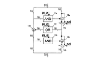
図11は、FL関数とFL-1関数の構成の一例を示す回路図である。FL関数は、1段目がANDゲート1aで2段目がORゲート2aである。FL-1関数はその逆に、1段目がORゲート2bで2段目がANDゲート1bである。
FIG. 11 is a circuit diagram showing an example of the configuration of the FL function and the FL −1 function. In the FL function, the first stage is an
FL関数および、FL-1関数の入力32bitは、16bit毎の2つのデータに分割され、排他的論理和(XOR:Exclusive OR)、論理積(AND)、論理和(OR)によって変換が行われる。KLij(1≦i≦8,1≦j≦2)は、KLiの左からj番目の16bitデータである。ここで、KLiは拡大鍵のことであり、MISTY1では、拡大鍵処理を実行することで、128bitの秘密鍵Kから256bitの拡大鍵KLiを生成する。拡大鍵の生成法の詳細は非特許文献1に記されている。
The 32-bit input of the FL function and the FL- 1 function is divided into two 16-bit data, and conversion is performed by exclusive OR (XOR), logical product (AND), and logical sum (OR). . KL ij (1 ≦ i ≦ 8, 1 ≦ j ≦ 2) is j-th 16-bit data from the left of KL i . Here, KL i is an extended key, and in
FL関数において、入力32bitの上位16bitのビット列と拡大鍵の上位16bitKLi1とは、ANDゲート1aへ入力される。入力32bitの下位16bitのビット列とANDゲート1aの出力とは、XORゲート3aへ入力される。XORゲート3aの出力と拡大鍵の下位16bitKLi2とは、ORゲート2aへ入力される。入力32bitの上位16bitのビット列とORゲート2aの出力とは、XORゲート3bへ入力される。XORゲート3bの出力は、FL関数の出力32bitの上位16ビットとなり、XORゲート3aの出力は、FL関数の出力32bitの下位16ビットとなる。
In the FL function, the high-order 16-bit bit string of the
FL-1関数において、入力32bitの下位16bitのビット列と拡大鍵の下位16bitKLi2とは、ORゲート2bへ入力される。入力32bitの上位16bitのビット列とORゲート2bの出力とは、XORゲート3cへ入力される。XORゲート3cの出力と拡大鍵の上位16bitKLi1とは、ANDゲート1bへ入力される。入力32bitの下位16bitのビット列とANDゲート1bの出力とは、XORゲート3dへ入力される。XORゲート3cの出力は、FL-1関数の出力32bitの上位16ビットとなり、XORゲート3dの出力は、FL-1関数の出力32bitの下位16ビットとなる。
In the FL- 1 function, the lower 16-bit bit string of the
FL関数とFL-1関数の実装法の従来例1について以下に説明する。 Conventional example 1 of the mounting method of the FL function and the FL- 1 function will be described below.
暗号化処理と復号処理の両方に対応したハードウェアを実装する場合、FL関数とFL-1関数の2つを実装する必要がある。図12は、従来例1の実装法を示す回路図である。これは、暗号化処理と復号処理に応じて、FL関数6とFL-1関数7をセレクタ5で切り替えることができるハードウェアである。
When implementing hardware that supports both encryption processing and decryption processing, it is necessary to implement two functions, the FL function and the FL- 1 function. FIG. 12 is a circuit diagram showing a mounting method of the first conventional example. This is hardware capable of switching between the FL function 6 and the FL- 1
FL関数とFL-1関数の実装法の従来例2について以下に説明する。 Conventional example 2 of the implementation method of the FL function and the FL- 1 function will be described below.
FL関数とFL-1関数の実装に関して、小型化を狙った実装法がある(例えば、特許文献1)。図13は、従来例2の実装法を示す回路図である。従来例2は、ANDゲート1cとORゲート2cをそれぞれ1個ずつのみ用いて実装する。つまり、2つの関数の共通部分であるANDゲートとORゲートの両方を共用化し、1つの関数にマージしている。
Regarding the implementation of the FL function and the FL- 1 function, there is an implementation method aimed at miniaturization (for example, Patent Document 1). FIG. 13 is a circuit diagram showing a mounting method of Conventional Example 2. Conventional example 2 is implemented using only one AND gate 1c and one
従来例2の関数において、入力32bitの下位16bitのビット列とANDゲート1cの出力とは、XORゲート3eへ入力される。入力32bitの上位16bitのビット列とORゲート2cの出力とは、XORゲート3fへ入力される。入力32bitの上位16bitのビット列とXORゲート3fの出力とは、セレクタ5aへ入力される。入力32bitの下位16bitのビット列とXORゲート3eの出力とは、セレクタ5bへ入力される。セレクタ5aの出力と拡大鍵の上位16bitKLi1とは、ANDゲート1cへ入力される。セレクタ5bの出力と拡大鍵の下位16bitKLi2とは、ORゲート2cへ入力される。XORゲート3fの出力は、従来例2の関数の出力32bitの上位16ビットとなり、XORゲート3eの出力は、従来例2の関数の出力32bitの下位16ビットとなる。
In the function of Conventional Example 2, the lower 16-bit bit string of the
セレクタ5a,5bにおいて、2入力のうち、上部信号が選択された場合は、この関数はFL関数として機能し、下段信号が選択された場合は、FL-1関数として機能する。この技術を用いると、回路規模を大きく削減することが可能である。
In the
しかしながら、従来例2は、組み合わせ回路のフィードバックループを形成するという重大な問題点を抱えている。従来例2に示される通り、どちらの関数として機能する場合においても、経路中にレジスタが含まれない、且つ組み合わせ回路のみのループ構造を形成している。この構造が存在すると、ハードウェア記述言語から回路構造への変換作業である論理合成を行うことが非常に困難になる。仮に論理合成が可能となったとしても、変換後に生成された回路が発信回路になる危険性がある。そのため、信頼性という面において、上述のフィードバックループ構造をもつ回路は製品化不可能な実装法である。 However, Conventional Example 2 has a serious problem of forming a feedback loop of a combinational circuit. As shown in Conventional Example 2, in either case of functioning as a function, a register is not included in the path and a loop structure including only a combinational circuit is formed. If this structure exists, it is very difficult to perform logic synthesis, which is a conversion work from a hardware description language to a circuit structure. Even if logic synthesis is possible, there is a risk that a circuit generated after conversion becomes a transmission circuit. Therefore, in terms of reliability, a circuit having the above feedback loop structure is a packaging method that cannot be commercialized.
このように、FL関数とFL-1関数の機能を1つの関数としてマージしようとする場合、回路構成としてフィードバックループを形成せずに、回路規模の削減を実現することは容易ではない。そのため、従来のMISTY1、KASUMIに関する多くの特許出願や学術論文では、従来例1のように、FL関数とFL-1関数が独立に実装されている。 Thus, when trying to merge the functions of the FL function and the FL −1 function as one function, it is not easy to reduce the circuit scale without forming a feedback loop as the circuit configuration. Therefore, in many patent applications and academic papers related to the conventional MISTY1 and KASUMI, the FL function and the FL- 1 function are implemented independently as in Conventional Example 1.
本発明は上述した問題点を解決するためになされたものであり、フィードバックループの無い回路によって、FL関数とFL-1関数をマージした関数を実現する暗号処理装置を提供することを目的とする。 The present invention has been made to solve the above-described problems, and an object thereof is to provide a cryptographic processing device that realizes a function obtained by merging an FL function and an FL- 1 function by a circuit without a feedback loop. .
上述した課題を解決するため、本発明の一態様は、暗号処理におけるFL関数及びFL-1関数の少なくともいずれかの演算を行うことができる暗号処理装置であって、ANDゲート及びORゲートのうちいずれか一方であって、暗号処理装置の入力の2Nビットのうち上位Nビットである第1入力ビット列と拡大鍵の上位Nビット及び下位Nビットのいずれか一方に基づく第1拡大鍵ビット列とが入力される第1演算ゲートと、第1演算ゲートの出力と暗号処理装置の入力の2Nビットのうち下位Nビットである第2入力ビット列とが入力される第1XORゲートと、ANDゲート及びORゲートのうち第1演算ゲートと異種のゲートであって、第1XORゲートの出力と前記拡大鍵の上位Nビット及び下位Nビットのいずれか他方に基づく第2拡大鍵ビット列とが入力される第2演算ゲートと、第2演算ゲートの出力と第1入力ビット列とが入力される第2XORゲートと、ANDゲート及びORゲートのうち第1演算ゲートと同種のゲートであって、第2XORゲートの出力と前記第1拡大鍵ビット列とが入力される第3演算ゲートと、第3演算ゲートの出力と第1XORゲートの出力とが入力される第3XORゲートとを有する。 In order to solve the above-described problem, one embodiment of the present invention is a cryptographic processing apparatus capable of performing at least one of an FL function and an FL- 1 function in cryptographic processing, and includes an AND gate and an OR gate. Any one of the first input bit string that is the upper N bits of the 2N bits of the input of the cryptographic processor and the first expanded key bit string based on either the upper N bits or the lower N bits of the expanded key A first XOR gate, a first XOR gate to which an output of the first arithmetic gate and a second input bit string which is a lower N bit out of 2N bits of the input of the cryptographic processor are input, an AND gate, and an OR gate Are different from the first operation gate based on the output of the first XOR gate and the higher N bits or the lower N bits of the expanded key. A second operation gate to which two expanded key bit sequences are input; a second XOR gate to which the output of the second operation gate and the first input bit sequence are input; and the same type as the first operation gate of the AND gate and the OR gate A third operation gate to which the output of the second XOR gate and the first extended key bit string are input, and a third XOR gate to which the output of the third operation gate and the output of the first XOR gate are input Have.
開示の暗号処理装置によれば、フィードバックループの無い回路によって、FL関数とFL-1関数をマージした関数を実現することができる。 According to the disclosed cryptographic processing apparatus, a function obtained by merging the FL function and the FL- 1 function can be realized by a circuit without a feedback loop.
以下、本発明の実施の形態について図面を参照しつつ説明する。 Embodiments of the present invention will be described below with reference to the drawings.
本発明は、MISTY1、MISTY2、KASUMI、CAMELLIAなど、FL関数とFL-1関数を採用する共通鍵暗号方式において、FL関数とFL-1関数を1つの関数として効率よくマージする新たな関数を用いることで、小型ハードウェアを実現する。本発明は、小型な共通鍵暗号ハードウェアを作る時に適用可能である。 The present invention uses a new function that efficiently merges the FL function and the FL -1 function as one function in a common key cryptosystem employing the FL function and the FL -1 function, such as MISTY1, MISTY2, KASUMI, and CAMELLIA. In this way, small hardware is realized. The present invention is applicable when making a small common key encryption hardware.
以下、MISTY1において、FL関数とFL-1関数を1つにマージしたマージ関数の例を示す。MISTY2やKASUMI、CAMELLIAなどに適用する場合も、基本的な考え方はMISTY1の場合と同様である。 An example of a merge function obtained by merging the FL function and the FL- 1 function into one in MISTY1 will be described below. When applied to MISTY2, KASUMI, CAMELLIA, etc., the basic concept is the same as in MISTY1.
(実施例1)
図1は、実施例1のマージ関数の構成の一例を示す回路図である。上述したように、FL関数は、1段目がANDゲートで2段目がORゲートである、2段構造を持つ関数である。FL-1関数はその逆に、1段目がORゲートで2段目がANDゲートである、2段構造を持つ関数である。これに対して、本実施例のマージ関数は、3段構造を持つ関数である。本実施例のマージ関数は、1段目をANDゲート11a(第1演算ゲート)、2段目をORゲート12(第2演算ゲート)、3段目をANDゲート11b(第3演算ゲート)とし、2つの関数の共通部分をORゲート12のみとする。
Example 1
FIG. 1 is a circuit diagram illustrating an example of a configuration of a merge function according to the first embodiment. As described above, the FL function is a function having a two-stage structure in which the first stage is an AND gate and the second stage is an OR gate. Conversely, the FL -1 function is a function having a two-stage structure in which the first stage is an OR gate and the second stage is an AND gate. On the other hand, the merge function of the present embodiment is a function having a three-stage structure. In the merge function of this embodiment, the first stage is an AND
このマージ関数の入力32bitは、上位16bitの入力上位ビット列(第1入力ビット列)と下位16bitの入力下位ビット列(第2入力ビット列)に分割される。ここで、N=16とする。
The
入力上位ビット列と拡大鍵の上位16bitであるKLi1とがANDゲート11aへ入力される。入力下位ビット列とANDゲート11aの出力がXORゲート13a(第1XORゲート)へ入力される。XORゲート13aの出力と入力下位ビット列とがセレクタ14a(第1セレクタ)へ入力される。
The input upper bit string and KL i1 which is the upper 16 bits of the extended key are input to the AND
セレクタ14aの出力と拡大鍵の下位16bitであるKLi2(第2拡大鍵ビット列)とがORゲート12へ入力される。入力上位ビット列とORゲート12の出力とがXORゲート13b(第2XORゲート)へ入力される。
The output of the
XORゲート13bの出力とKLi1とがANDゲート11bへ入力される。セレクタ14aの出力とANDゲート11bの出力とがXORゲート13c(第3XORゲート)へ入力される。XORゲート13cの出力とセレクタ14aの出力とがセレクタ14b(第2セレクタ)へ入力される。
The output of the
XORゲート13bの出力は、マージ関数の出力32bitの上位16bitとなる。セレクタ14bの出力は、マージ関数の出力32bitの下位16bitとなる。
The output of the
セレクタ14a,14bは、選択信号selにより2入力の一方を選択して出力する。マージ関数がFL関数の指示を受けた場合、セレクタ14aがXORゲート13aの出力を選択し、且つセレクタ14bがセレクタ14aの出力を選択することにより、このマージ関数は、FL関数として機能する。マージ関数がFL-1関数の指示を受けた場合、セレクタ14aが入力下位ビット列を選択し、且つセレクタ14bがXORゲート13cの出力を選択することにより、このマージ関数は、FL-1関数として機能する。
The
このように、ANDゲートとORゲートの2つを共通部分とするのではなく、ORゲート12のみを共通部分とすることによって、フィードバックループの形成を回避することができる。
Thus, the formation of a feedback loop can be avoided by using only the
1つの関数にマージしたことにより、16bitANDゲートと16bitXORゲート分の回路規模(56gate)が削減される。そのため、従来の従来例1の回路規模が0.18umプロセスで約336gateなのに対し、実施例1の回路規模は約280gateとなる。 By merging into one function, the circuit scale (56 gate) for the 16-bit AND gate and the 16-bit XOR gate is reduced. Therefore, the circuit scale of the conventional example 1 is about 336 gates in the 0.18 um process, whereas the circuit scale of the example 1 is about 280 gates.
実施例1の回路規模を更に削減するために、実施例1におけるセレクタをANDゲートへと等価変換する。 In order to further reduce the circuit scale of the first embodiment, the selector in the first embodiment is equivalently converted to an AND gate.
(実施例2)
図2は、実施例2のマージ関数の構成の一例を示す回路図である。この図において、図1と同一符号は図1に示された対象と同一又は相当物を示しており、ここでの説明を省略する。本実施例は、実施例1のセレクタ14a,14bをそれぞれXORゲート13a,13cの入力側へと移動させてセレクタ15a(第3セレクタ),15b(第4セレクタ)とする。これによって、セレクタ15a,15bはそれぞれANDゲート11a,11bの出力信号、もしくは16bitの0信号のどちらかを選択するように変更できる。
(Example 2)
FIG. 2 is a circuit diagram illustrating an example of the configuration of the merge function according to the second embodiment. In this figure, the same reference numerals as those in FIG. 1 denote the same or corresponding parts as those in FIG. 1, and the description thereof is omitted here. In the present embodiment, the
マージ関数がFL関数の指示を受けた場合、セレクタ15aがANDゲート11aの出力を選択し、且つセレクタ15bが0信号を選択することにより、このマージ関数は、FL関数として機能する。マージ関数がFL-1関数の指示を受けた場合、セレクタ15aが0信号を選択し、且つセレクタ15bがANDゲート11bの出力を選択することにより、このマージ関数は、FL-1関数として機能する。
When the merge function receives an instruction of the FL function, the
(実施例3)
図3は、実施例3のマージ関数の構成の一例を示す回路図である。この図において、図2と同一符号は図2に示された対象と同一又は相当物を示しており、ここでの説明を省略する。本実施例は、実施例2におけるセレクタ15a,15bをそれぞれANDゲート16a(第1ANDゲート),16b(第2ANDゲート)に等価変換する。実施例2では、セレクタにおける選択信号selは1bitであるが、実施例3では16bitに拡張した信号である。
(Example 3)
FIG. 3 is a circuit diagram illustrating an example of the configuration of the merge function according to the third embodiment. In this figure, the same reference numerals as those in FIG. 2 denote the same or corresponding parts as those in FIG. 2, and the description thereof will be omitted here. In this embodiment, the
ANDゲート16aは、ANDゲート11aの出力と選択信号selとのAND演算を行う。ANDゲート16bは、ANDゲート11bの出力と選択信号selの否定信号とのAND演算を行う。
The AND
このようにセレクタをANDゲートに変換することにより、実施例1における回路規模をさらに削減することができる。 Thus, by converting the selector into an AND gate, the circuit scale in the first embodiment can be further reduced.
(実施例4)
FL関数とFL-1関数を1つの関数としてマージを行うことにより、クリティカルパスが延長され、処理速度の低下を引き起こす場合がある。
Example 4
When the merge is performed using the FL function and the FL- 1 function as one function, the critical path may be extended and the processing speed may be reduced.
ここで、2−1NANDゲートの遅延をdとする。ANDゲート、ORゲート、XORゲート、セレクタをNANDゲートのみで構成する場合、各ゲートの遅延は、2d、2d、3d、3dとなる。 Here, the delay of the 2-1 NAND gate is d. When the AND gate, OR gate, XOR gate, and selector are composed of only NAND gates, the delay of each gate is 2d, 2d, 3d, 3d.
従来例1のクリティカルパスは、FLもしくはFL-1の遅延が10d(FLにおける(1段目:AND−XOR)+(2段目:OR−XOR)、もしくはFL-1における(1段目:OR−XOR)+(2段目:AND−XOR)より(2d+3d)+(2d+3d)=10d)、FLとFL-1をセレクトするセレクタが3dのため、計13dとなる。 Critical path of the conventional example 1, a delay 10d (in FL (1-stage FL or FL -1: AND-XOR) + (2 stage: OR-XOR), or in the FL -1 (1 stage: (2d + 3d) + (2d + 3d) = 10d) from (OR-XOR) + (second stage: AND-XOR), and the selector for selecting FL and FL −1 is 3d, so the total is 13d.
一方、実施例2におけるクリティカルパスは、(1段目:AND−sel−XOR)+(2段目:OR−XOR)+(3段目:AND−sel−XOR)=(2d+3d+3d)+(2d+3d)+(2d+3d+3d)=21dとなる。
る。この理由は、従来例1では並列だったFL関数とFL-1関数に対して、実施例3では縦列の構造となっているためである。これを解決するために、実施例3で等価変換したANDゲートをクリティカルパス上から移動する。
On the other hand, the critical path in the second embodiment is (first stage: AND-sel-XOR) + (second stage: OR-XOR) + (third stage: AND-sel-XOR) = (2d + 3d + 3d) + (2d + 3d). ) + (2d + 3d + 3d) = 21d.
The The reason for this is that the FL function and FL -1 function that were parallel in the conventional example 1 have a column structure in the third embodiment. In order to solve this, the AND gate equivalently converted in the third embodiment is moved from the critical path.
図4は、実施例4のマージ関数の構成の一例を示す回路図である。この図において、図3と同一符号は図3に示された対象と同一又は相当物を示しており、ここでの説明を省略する。本実施例は、実施例3におけるANDゲート16a,16bをクリティカルパス上から移動してそれぞれANDゲート17a(第3ANDゲート),17b(第4ANDゲート)とする。
FIG. 4 is a circuit diagram illustrating an example of the configuration of the merge function according to the fourth embodiment. In this figure, the same reference numerals as those in FIG. 3 denote the same or corresponding parts as those in FIG. 3, and the description thereof is omitted here. In this embodiment, the AND
ANDゲート17aは、選択信号selとKLi1とのAND演算を行う。ANDゲート17bは、選択信号selの否定信号とKLi1とのAND演算を行う。
The AND
MISTY1では、拡大鍵であるKLijを生成するパスはクリティカルパスにならない。なぜなら、FL関数の処理サイクルより事前のサイクルでKLijを生成できる実装が多数知られており、これらの方法を用いることで、KLijの生成遅延時間の影響をFL関数の遅延時間に及ぼさない処理が可能であるからである。このMISTY1の性質を考慮することにより、実施例3のANDゲート16a,16bを本実施例のANDゲート17a,17bへ移動することができる。これにより、クリティカルパスの遅延がANDゲート2個分短縮される。つまり、(1段目:AND−XOR)+(2段目:OR−XOR)+(3段目:AND−XOR)=(2d+3d)+(2d+3d)+(2d+3d)=15dとなる。
In MISTY1, the path for generating the expanded key KL ij is not a critical path. This is because there are many known implementations that can generate KL ij in a cycle prior to the processing cycle of the FL function. By using these methods, the influence of the generation delay time of KL ij does not affect the delay time of the FL function. This is because processing is possible. By considering the property of MISTY1, the AND
(実施例5)
図5は、実施例5のマージ関数の構成の一例を示す回路図である。この図において、図1と同一符号は図1に示された対象と同一又は相当物を示しており、ここでの説明を省略する。本実施例は、基本的な構成と効果が実施例1と同様であるが、ORゲート及びANDゲートの配置が実施例1と異なる。実施例1では、FL関数とFL-1関数の共通部分をORゲートとしたが、本実施例ではANDゲートを共通部分としている。つまり、本実施例のマージ関数は、1段目をORゲート21a(第1演算ゲート)、2段目をANDゲート22(第2演算ゲート)、3段目をORゲート21b(第3演算ゲート)とし、2つの関数の共通部分をANDゲート22のみとする。
(Example 5)
FIG. 5 is a circuit diagram illustrating an example of the configuration of the merge function according to the fifth embodiment. In this figure, the same reference numerals as those in FIG. 1 denote the same or corresponding parts as those in FIG. 1, and the description thereof is omitted here. This embodiment has the same basic configuration and effect as the first embodiment, but the arrangement of OR gates and AND gates is different from the first embodiment. In the first embodiment, the common part of the FL function and the FL −1 function is an OR gate, but in this embodiment, the AND gate is a common part. That is, the merge function of the present embodiment has the first stage of the
ORゲート21aの出力にXORゲート13aの入力が接続される。ANDゲート22の出力にXORゲート13bの入力が接続される。ORゲート21bの出力にXORゲート13cの入力が接続される。
The input of the
(実施例6)
図6は、実施例6のマージ関数の構成の一例を示す回路図である。この図において、図5と同一符号は図5に示された対象と同一又は相当物を示しており、ここでの説明を省略する。本実施例は、実施例5のセレクタ14a,14bをそれぞれXORゲート13a,13cの入力側へと移動させてセレクタ15a,15bとする。本実施例は、基本的な構成と効果が実施例2と同様であるが、ORゲート及びANDゲートの配置が実施例2と異なる。
(Example 6)
FIG. 6 is a circuit diagram illustrating an example of the configuration of the merge function according to the sixth embodiment. In this figure, the same reference numerals as those in FIG. 5 denote the same or corresponding parts as those in FIG. 5, and a description thereof will be omitted here. In the present embodiment, the
(実施例7)
図7は、実施例7のマージ関数の構成の一例を示す回路図である。この図において、図6と同一符号は図6に示された対象と同一又は相当物を示しており、ここでの説明を省略する。本実施例は、実施例6におけるセレクタ15a,15bをそれぞれANDゲート16a,16bに等価変換する。本実施例は、基本的な構成と効果が実施例3と同様であるが、ORゲート及びANDゲートの配置が実施例3と異なる。
(Example 7)
FIG. 7 is a circuit diagram illustrating an example of the configuration of the merge function according to the seventh embodiment. In this figure, the same reference numerals as those in FIG. 6 denote the same or corresponding parts as those in FIG. 6, and the description thereof is omitted here. In this embodiment, the
上述の各実施例の効果について以下に説明する。 The effects of the above embodiments will be described below.
図8は、各実施例の回路規模の一例を示す表である。この表は、実施例1〜7と従来例1,2のそれぞれにおける回路規模の一例を示す。この表において、#1−bit MUXは、1−bit幅のセレクタの個数を示し、#1−bit AND/ORは、1−bit幅のANDゲート及びORゲートの個数を示し、#1−bit XORは、1−bit幅のXORゲートの個数を示し、Gate Countは、FL関数とFL-1関数に関する回路規模を示す。従来例1は、FL関数とFL-1関数をそれぞれ独立に持っており、これらを切り替えるセレクタも必要とするため、回路規模が336gateと大きくなっている。従来例2は、回路規模は小さくなっているものの、フィードバックループ構造を持つために製品化不可能な実装である。実施例1、2では従来例1と比較して、回路規模は削減されるものの、その効果は小さい。この理由は、セレクタの回路規模が同一だからである。実施例3、4では、この実施例1におけるセレクタをANDゲートへと等価変換することによって、200gateまで回路規模を削減している。 FIG. 8 is a table showing an example of the circuit scale of each embodiment. This table shows an example of the circuit scale in each of Examples 1 to 7 and Conventional Examples 1 and 2. In this table, # 1-bit MUX indicates the number of 1-bit width selectors, # 1-bit AND / OR indicates the number of 1-bit width AND gates and OR gates, and # 1-bit XOR indicates the number of 1-bit width XOR gates, and Gate Count indicates the circuit scale related to the FL function and the FL −1 function. Conventional example 1 has an FL function and an FL −1 function independently, and also requires a selector for switching between them, so that the circuit scale is as large as 336 gates. Conventional Example 2 is a packaging that cannot be commercialized because it has a feedback loop structure although the circuit scale is small. In the first and second embodiments, the circuit scale is reduced as compared with the conventional example 1, but the effect is small. This is because the circuit scale of the selector is the same. In the third and fourth embodiments, the circuit scale is reduced to 200 gates by equivalently converting the selector in the first embodiment into an AND gate.
以上より、従来例1と実施例4を比較すると、本発明により、FL関数とFL-1関数に関する回路規模が336gateから200gateへと約40%削減されることが見積もれた。 From the above, comparing Conventional Example 1 and Example 4, it was estimated that the circuit scale of the FL function and the FL −1 function is reduced by about 40% from 336 gate to 200 gate according to the present invention.
従来の小型化されたMISTY1ハードウェア(0.18umプロセスで約4000gate、例えば、非特許文献2を参照)に実施例4を適用すると、約3.5%の回路規模の削減効果が期待できる。
When Example 4 is applied to conventional miniaturized MISTY1 hardware (about 4000 gate with 0.18 um process, see
従来の小型化されたKASUMIハードウェア(0.13umプロセスで約3400gate:例えば、非特許文献3を参照)に実施例4を適用すると、最大で4%の回路規模の削減効果が期待できる。 When Example 4 is applied to conventional miniaturized KASUMI hardware (about 3400 gate with 0.13 um process: see, for example, Non-Patent Document 3), a circuit size reduction effect of up to 4% can be expected.
図9は、各実施例の遅延時間の一例を示す表である。この表は、実施例1〜7と従来例1,2のそれぞれにおける遅延時間の一例を示す。この表において、AND/ORは、マージ関数におけるANDゲート及びORゲートの数を示し、XORは、マージ関数におけるXORゲートの数を示し、2−1MUXは、マージ関数におけるセレクタの数を示し、遅延は、マージ関数の遅延時間を示す。従来例1では、遅延時間が13dであるが、実施例1では21dと大きく増加している。これは前述の通り、マージ関数が3段構造をとっており、さらに新たなセレクタがマージ関数の内部に生成されたためである。実施例3では、セレクタをANDゲートへと等価変換したことにより、2dだけ遅延時間が短縮されたものの、従来例1と比較すると大きい。実施例4において、クリティカルパス上からANDゲートを2つ分移動することにより、遅延時間が15dとなり、従来例1の13dとほぼ同等の遅延時間となる。 FIG. 9 is a table showing an example of the delay time of each embodiment. This table shows an example of the delay time in each of Examples 1 to 7 and Conventional Examples 1 and 2. In this table, AND / OR indicates the number of AND gates and OR gates in the merge function, XOR indicates the number of XOR gates in the merge function, 2-1MUX indicates the number of selectors in the merge function, and delay Indicates the delay time of the merge function. In the first conventional example, the delay time is 13d, but in the first example, the delay time is greatly increased to 21d. As described above, this is because the merge function has a three-stage structure, and a new selector is generated inside the merge function. In the third embodiment, although the delay time is reduced by 2d due to equivalent conversion of the selector to the AND gate, it is larger than the first conventional example. In the fourth embodiment, by moving two AND gates on the critical path, the delay time becomes 15d, which is substantially the same as 13d in the first conventional example.
実施例1、5によれば、ANDゲートとORゲートの2つを共通モジュールしてマージを行うのではなく、ANDゲート、もしくはORゲートのどちらか一方のみを共通モジュールとして、マージを行うことにより、フィードバックループの形成を回避することができる。 According to the first and fifth embodiments, the merge is performed by using only one of the AND gate and the OR gate as a common module instead of performing the merge by using the AND gate and the OR gate as a common module. The formation of a feedback loop can be avoided.
実施例2、3、4、6、7によれば、回路規模の増加とクリティカルパス延長の原因となっているセレクタをANDゲートへと等価変換することによって、回路規模の削減を行い、さらにこのANDゲートをクリティカルパス以外の部分へと移動させることによって、クリティカルパスの短縮を図ることができる。 According to the second, third, fourth, sixth, and seventh embodiments, the circuit scale is reduced by equivalently converting the selector causing the increase in the circuit scale and the extension of the critical path into an AND gate. The critical path can be shortened by moving the AND gate to a portion other than the critical path.
上述の各実施例によれば、フィードバックループを形成せずに、大幅な回路規模の削減、ならびにクリティカルパスの延長を最大限に抑制する回路構造を実現する。 According to each of the above-described embodiments, a circuit structure that significantly reduces the circuit scale and suppresses the extension of the critical path without realizing a feedback loop is realized.
実施例1〜4において、第1拡大鍵ビット列は、KLi1に基づくANDゲートの入力に対応し、第2拡大鍵ビット列は、KLi2に基づくORゲートの入力に対応する。実施例5〜7において、第1拡大鍵ビット列は、KLi2に基づくORゲートの入力に対応し、第2拡大鍵ビット列は、KLi1に基づくANDゲートの入力に対応する。 In the first to fourth embodiments, the first extended key bit string corresponds to the input of the AND gate based on KL i1 , and the second extended key bit string corresponds to the input of the OR gate based on KL i2 . In the fifth to seventh embodiments, the first extended key bit string corresponds to the input of the OR gate based on KL i2 , and the second extended key bit string corresponds to the input of the AND gate based on KL i1 .
本発明は、その精神または主要な特徴から逸脱することなく、他の様々な形で実施することができる。そのため、前述の実施の形態は、あらゆる点で単なる例示に過ぎず、限定的に解釈してはならない。本発明の範囲は、特許請求の範囲によって示すものであって、明細書本文には、何ら拘束されない。更に、特許請求の範囲の均等範囲に属する全ての変形、様々な改良、代替および改質は、全て本発明の範囲内のものである。 The present invention can be implemented in various other forms without departing from the spirit or main features thereof. Therefore, the above-described embodiment is merely an example in all respects and should not be interpreted in a limited manner. The scope of the present invention is shown by the scope of claims, and is not restricted by the text of the specification. Moreover, all modifications, various improvements, substitutions and modifications belonging to the equivalent scope of the claims are all within the scope of the present invention.
以上の実施例1〜7を含む実施形態に関し、更に以下の付記を開示する。
(付記1)
暗号処理におけるFL関数及びFL-1関数の演算を行うことができる暗号処理装置であって、
ANDゲート及びORゲートのうちいずれか一方であって、前記暗号処理装置の入力の2Nビットのうち上位Nビットである第1入力ビット列と拡大鍵の上位Nビット及び下位Nビットのいずれか一方に基づく第1拡大鍵ビット列とが入力される第1演算ゲートと、
前記第1演算ゲートの出力と前記暗号処理装置の入力の2Nビットのうち下位Nビットである第2入力ビット列とが入力される第1XORゲートと、
ANDゲート及びORゲートのうち前記第1演算ゲートと異種のゲートであって、前記第1XORゲートの出力と前記拡大鍵の上位Nビット及び下位Nビットのいずれか他方に基づく第2拡大鍵ビット列とが入力される第2演算ゲートと、
前記第2演算ゲートの出力と前記第1入力ビット列とが入力される第2XORゲートと、
ANDゲート及びORゲートのうち前記第1演算ゲートと同種のゲートであって、前記第2XORゲートの出力と前記第1拡大鍵ビット列とが入力される第3演算ゲートと、
前記第3演算ゲートの出力と前記第1XORゲートの出力とが入力される第3XORゲートと、
を備える暗号処理装置。
(付記2)
更に、
選択信号に基づいて、前記第1XORゲートの出力と前記第2入力ビット列とのいずれかを選択して前記第2演算ゲート及び前記第3XORゲートへ出力する第1セレクタと、
前記選択信号に基づいて、前記第3XORゲートの出力と前記第1セレクタの出力とのいずれかを選択して出力する第2セレクタと、
を備える、
付記1に記載の暗号処理装置。
(付記3)
FL関数の指示を受けた前記第1セレクタは、前記第1XORゲートの出力を選択し、
FL関数の指示を受けた前記第2セレクタは、前記第1セレクタの出力を選択し、
FL-1関数の指示を受けた前記第1セレクタは、前記第2入力ビット列を選択し、
FL-1関数の指示を受けた前記第2セレクタは、前記第3XORゲートの出力を選択する、
付記2に記載の暗号処理装置。
(付記4)
更に、
選択信号に基づいて、前記第1演算ゲートの出力と前記Nビットの0信号とのいずれかを選択して前記第1XORゲートへ出力する第3セレクタと、
前記選択信号に基づいて、前記第3演算ゲートの出力と前記Nビットの0信号とのいずれかを選択して前記第3XORゲートへ出力する第4セレクタと、
を備える、
付記1に記載の暗号処理装置。
(付記5)
FL関数の指示を受けた前記第3セレクタは、前記第1演算ゲートの出力を選択し、
FL関数の指示を受けた前記第4セレクタは、前記Nビットの0信号を選択し、
FL-1関数の指示を受けた前記第3セレクタは、前記Nビットの0信号を選択し、
FL-1関数の指示を受けた前記第4セレクタは、前記第3演算ゲートの出力を選択する、
付記4に記載の暗号処理装置。
(付記6)
更に、
前記第1演算ゲートの出力と選択信号とのAND演算を行って前記第1XORゲートへ出力する第1ANDゲートと、
前記第3演算ゲートの出力と前記選択信号の否定信号とのAND演算を行って前記第3XORゲートへ出力する第3ANDゲートと、
を備える、
付記1に記載の暗号処理装置。
(付記7)
更に、
前記拡大鍵の上位Nビットと選択信号とのAND演算を行って前記第1演算ゲートへ出力する第3ANDゲートと、
前記拡大鍵の上位Nビットと前記選択信号の否定信号とのAND演算を行って前記第3演算ゲートへ出力する第4ANDゲートと、
を備え、
前記第1演算ゲート及び前記第3演算ゲートは、ANDゲートであり、
前記第2演算ゲートは、ORゲートである、
付記1に記載の暗号処理装置。
(付記8)
前記第1演算ゲート及び前記第3演算ゲートは、ANDゲートであり、
前記第2演算ゲートは、ORゲートである、
付記1に記載の暗号処理装置。
(付記9)
前記第1演算ゲート及び前記第3演算ゲートは、ORゲートであり、
前記第2演算ゲートは、ANDゲートである、
付記1に記載の暗号処理装置。
(付記10)
前記第1演算ゲート、前記第1XORゲート、前記第2ゲート、前記第2XORゲート、前記演算第3ゲート、前記第3XORゲートは、共通鍵暗号のアルゴリズムのMISTY1におけるFL関数及びFL-1関数に設けられる、
付記1に記載の暗号処理装置。
(付記11)
前記第1演算ゲート、前記第1XORゲート、前記第2ゲート、前記第2XORゲート、前記演算第3ゲート、前記第3XORゲートは、共通鍵暗号のアルゴリズムのMISTY2におけるFL関数及びFL-1関数に設けられる、
付記1に記載の暗号処理装置。
(付記12)
前記第1演算ゲート、前記第1XORゲート、前記第2ゲート、前記第2XORゲート、前記演算第3ゲート、前記第3XORゲートは、共通鍵暗号のアルゴリズムのKASUMIにおけるFL関数及びFL-1関数に設けられる、
付記1に記載の暗号処理装置。
(付記13)
前記第1演算ゲート、前記第1XORゲート、前記第2ゲート、前記第2XORゲート、前記演算第3ゲート、前記第3XORゲートは、共通鍵暗号のアルゴリズムのCAMELLIAにおけるFL関数及びFL-1関数に設けられる、
付記1に記載の暗号処理装置。
Regarding the embodiment including the above Examples 1 to 7, the following additional notes are further disclosed.
(Appendix 1)
A cryptographic processing apparatus capable of performing calculations of FL function and FL -1 function in cryptographic processing,
Any one of an AND gate and an OR gate, and the first input bit string which is the upper N bits of the 2N bits of the input of the cryptographic processing device and either the upper N bits or the lower N bits of the extended key A first operation gate to which a first expanded key bit string based on the first operation gate is input;
A first XOR gate to which an output of the first arithmetic gate and a second input bit string that is a lower N bit among 2N bits of an input of the cryptographic processor are input;
Of the AND gate and the OR gate, the gate is different from the first operation gate, and a second extended key bit string based on the output of the first XOR gate and either the upper N bits or the lower N bits of the extended key; A second arithmetic gate to which is input;
A second XOR gate to which an output of the second operation gate and the first input bit string are input;
A third arithmetic gate that is the same type of gate as the first arithmetic gate among the AND gate and the OR gate, and that receives the output of the second XOR gate and the first extended key bit string;
A third XOR gate to which an output of the third arithmetic gate and an output of the first XOR gate are input;
A cryptographic processing apparatus comprising:
(Appendix 2)
Furthermore,
A first selector that selects one of the output of the first XOR gate and the second input bit string based on a selection signal and outputs the selected one to the second arithmetic gate and the third XOR gate;
A second selector that selects and outputs either the output of the third XOR gate or the output of the first selector based on the selection signal;
Comprising
The cryptographic processing apparatus according to
(Appendix 3)
The first selector that receives the instruction of the FL function selects the output of the first XOR gate,
The second selector receiving the instruction of the FL function selects the output of the first selector,
The first selector receiving the instruction of the FL -1 function selects the second input bit string,
The second selector receiving the instruction of the FL -1 function selects the output of the third XOR gate.
The cryptographic processing apparatus according to
(Appendix 4)
Furthermore,
A third selector that selects either the output of the first operation gate or the N-
A fourth selector that selects either the output of the third operation gate or the N-
Comprising
The cryptographic processing apparatus according to
(Appendix 5)
The third selector receiving the instruction of the FL function selects the output of the first arithmetic gate,
The fourth selector receiving the instruction of the FL function selects the N-
The third selector receiving the instruction of the FL −1 function selects the N-
The fourth selector receiving the instruction of the FL -1 function selects the output of the third arithmetic gate.
The cryptographic processing apparatus according to
(Appendix 6)
Furthermore,
A first AND gate that performs an AND operation on an output of the first operation gate and a selection signal and outputs the result to the first XOR gate;
A third AND gate that performs an AND operation on an output of the third operation gate and a negative signal of the selection signal and outputs the result to the third XOR gate;
Comprising
The cryptographic processing apparatus according to
(Appendix 7)
Furthermore,
A third AND gate that performs an AND operation on the upper N bits of the expanded key and a selection signal and outputs the result to the first operation gate;
A fourth AND gate that performs an AND operation on the upper N bits of the expanded key and a negative signal of the selection signal and outputs the result to the third operation gate;
With
The first operation gate and the third operation gate are AND gates;
The second operation gate is an OR gate;
The cryptographic processing apparatus according to
(Appendix 8)
The first operation gate and the third operation gate are AND gates;
The second operation gate is an OR gate;
The cryptographic processing apparatus according to
(Appendix 9)
The first operation gate and the third operation gate are OR gates,
The second operation gate is an AND gate;
The cryptographic processing apparatus according to
(Appendix 10)
The first operation gate, the first XOR gate, the second gate, the second XOR gate, the third operation gate, and the third XOR gate are provided in the FL function and the FL −1 function in the MISTY1 of the common key encryption algorithm. Be
The cryptographic processing apparatus according to
(Appendix 11)
The first arithmetic gate, the first XOR gate, the second gate, the second XOR gate, the third arithmetic gate, and the third XOR gate are provided in the FL function and the FL −1 function in the MISTY2 of the common key encryption algorithm. Be
The cryptographic processing apparatus according to
(Appendix 12)
The first operation gate, the first XOR gate, the second gate, the second XOR gate, the operation third gate, and the third XOR gate are provided in the FL function and the FL −1 function in the KASUMI of the common key encryption algorithm. Be
The cryptographic processing apparatus according to
(Appendix 13)
The first operation gate, the first XOR gate, the second gate, the second XOR gate, the operation third gate, and the third XOR gate are provided in the FL function and the FL −1 function in the CAMELLIA of the common key encryption algorithm. Be
The cryptographic processing apparatus according to
11a,11b,22,16a,16b,17a,17b ANDゲート
12,21a,21b ORゲート
13a,13b,13c XORゲート
14a,14b,15a,15b セレクタ
11a, 11b, 22, 16a, 16b, 17a, 17b AND
Claims (5)
ANDゲート及びORゲートのうちいずれか一方であって、前記暗号処理装置の入力の2Nビットのうち上位Nビットである第1入力ビット列と拡大鍵の上位Nビット及び下位Nビットのいずれか一方に基づく第1拡大鍵ビット列とが入力される第1演算ゲートと、
前記第1演算ゲートの出力と前記暗号処理装置の入力の2Nビットのうち下位Nビットである第2入力ビット列とが入力される第1XORゲートと、
ANDゲート及びORゲートのうち前記第1演算ゲートと異種のゲートであって、前記第1XORゲートの出力と前記拡大鍵の上位Nビット及び下位Nビットのいずれか他方に基づく第2拡大鍵ビット列とが入力される第2演算ゲートと、
前記第2演算ゲートの出力と前記第1入力ビット列とが入力される第2XORゲートと、
ANDゲート及びORゲートのうち前記第1演算ゲートと同種のゲートであって、前記第2XORゲートの出力と前記第1拡大鍵ビット列とが入力される第3演算ゲートと、
前記第3演算ゲートの出力と前記第1XORゲートの出力とが入力される第3XORゲートと、
を備える暗号処理装置。 A cryptographic processing apparatus capable of performing calculations of FL function and FL -1 function in cryptographic processing,
Any one of an AND gate and an OR gate, and the first input bit string which is the upper N bits of the 2N bits of the input of the cryptographic processing device and either the upper N bits or the lower N bits of the extended key A first operation gate to which a first expanded key bit string based on the first operation gate is input;
A first XOR gate to which an output of the first arithmetic gate and a second input bit string that is a lower N bit among 2N bits of an input of the cryptographic processor are input;
Of the AND gate and the OR gate, the gate is different from the first operation gate, and a second extended key bit string based on the output of the first XOR gate and either the upper N bits or the lower N bits of the extended key; A second arithmetic gate to which is input;
A second XOR gate to which an output of the second operation gate and the first input bit string are input;
A third arithmetic gate that is the same type of gate as the first arithmetic gate among the AND gate and the OR gate, and that receives the output of the second XOR gate and the first extended key bit string;
A third XOR gate to which an output of the third arithmetic gate and an output of the first XOR gate are input;
A cryptographic processing apparatus comprising:
選択信号に基づいて、前記第1XORゲートの出力と前記第2入力ビット列とのいずれかを選択して前記第2演算ゲート及び前記第3XORゲートへ出力する第1セレクタと、
前記選択信号に基づいて、前記第3XORゲートの出力と前記第1セレクタの出力とのいずれかを選択して出力する第2セレクタと、
を備える、
請求項1に記載の暗号処理装置。 Furthermore,
A first selector that selects one of the output of the first XOR gate and the second input bit string based on a selection signal and outputs the selected one to the second arithmetic gate and the third XOR gate;
A second selector that selects and outputs either the output of the third XOR gate or the output of the first selector based on the selection signal;
Comprising
The cryptographic processing apparatus according to claim 1.
選択信号に基づいて、前記第1演算ゲートの出力と前記Nビットの0信号とのいずれかを選択して前記第1XORゲートへ出力する第3セレクタと、
前記選択信号に基づいて、前記第3演算ゲートの出力と前記Nビットの0信号とのいずれかを選択して前記第3XORゲートへ出力する第4セレクタと、
を備える、
請求項1に記載の暗号処理装置。 Furthermore,
A third selector that selects either the output of the first operation gate or the N-bit 0 signal based on a selection signal and outputs the selected signal to the first XOR gate;
A fourth selector that selects either the output of the third operation gate or the N-bit 0 signal based on the selection signal and outputs the selected signal to the third XOR gate;
Comprising
The cryptographic processing apparatus according to claim 1.
前記第1演算ゲートの出力と選択信号とのAND演算を行って前記第1XORゲートへ出力する第1ANDゲートと、
前記第3演算ゲートの出力と前記選択信号の否定信号とのAND演算を行って前記第3XORゲートへ出力する第3ANDゲートと、
を備える、
請求項1に記載の暗号処理装置。 Furthermore,
A first AND gate that performs an AND operation on an output of the first operation gate and a selection signal and outputs the result to the first XOR gate;
A third AND gate that performs an AND operation on an output of the third operation gate and a negative signal of the selection signal and outputs the result to the third XOR gate;
Comprising
The cryptographic processing apparatus according to claim 1.
前記拡大鍵の上位Nビットと選択信号とのAND演算を行って前記第1演算ゲートへ出力する第3ANDゲートと、
前記拡大鍵の上位Nビットと前記選択信号の否定信号とのAND演算を行って前記第3演算ゲートへ出力する第4ANDゲートと、
を備え、
前記第1演算ゲート及び前記第3演算ゲートは、ANDゲートであり、
前記第2演算ゲートは、ORゲートである、
請求項1に記載の暗号処理装置。 Furthermore,
A third AND gate that performs an AND operation on the upper N bits of the expanded key and a selection signal and outputs the result to the first operation gate;
A fourth AND gate that performs an AND operation on the upper N bits of the expanded key and a negative signal of the selection signal and outputs the result to the third operation gate;
With
The first operation gate and the third operation gate are AND gates;
The second operation gate is an OR gate;
The cryptographic processing apparatus according to claim 1.
Priority Applications (3)
| Application Number | Priority Date | Filing Date | Title |
|---|---|---|---|
| JP2009007249A JP5200949B2 (en) | 2009-01-16 | 2009-01-16 | Cryptographic processing device |
| US12/612,290 US8111827B2 (en) | 2009-01-16 | 2009-11-04 | Cryptographic processing apparatus and cryptographic processing method |
| EP09176232.8A EP2209251B1 (en) | 2009-01-16 | 2009-11-17 | Cryptographic processing apparatus and cryptographic processing method |
Applications Claiming Priority (1)
| Application Number | Priority Date | Filing Date | Title |
|---|---|---|---|
| JP2009007249A JP5200949B2 (en) | 2009-01-16 | 2009-01-16 | Cryptographic processing device |
Publications (2)
| Publication Number | Publication Date |
|---|---|
| JP2010164792A JP2010164792A (en) | 2010-07-29 |
| JP5200949B2 true JP5200949B2 (en) | 2013-06-05 |
Family
ID=42135941
Family Applications (1)
| Application Number | Title | Priority Date | Filing Date |
|---|---|---|---|
| JP2009007249A Expired - Fee Related JP5200949B2 (en) | 2009-01-16 | 2009-01-16 | Cryptographic processing device |
Country Status (3)
| Country | Link |
|---|---|
| US (1) | US8111827B2 (en) |
| EP (1) | EP2209251B1 (en) |
| JP (1) | JP5200949B2 (en) |
Families Citing this family (7)
| Publication number | Priority date | Publication date | Assignee | Title |
|---|---|---|---|---|
| US8832464B2 (en) * | 2009-03-31 | 2014-09-09 | Oracle America, Inc. | Processor and method for implementing instruction support for hash algorithms |
| US20100250965A1 (en) * | 2009-03-31 | 2010-09-30 | Olson Christopher H | Apparatus and method for implementing instruction support for the advanced encryption standard (aes) algorithm |
| US8654970B2 (en) * | 2009-03-31 | 2014-02-18 | Oracle America, Inc. | Apparatus and method for implementing instruction support for the data encryption standard (DES) algorithm |
| US9317286B2 (en) * | 2009-03-31 | 2016-04-19 | Oracle America, Inc. | Apparatus and method for implementing instruction support for the camellia cipher algorithm |
| US20100246815A1 (en) * | 2009-03-31 | 2010-09-30 | Olson Christopher H | Apparatus and method for implementing instruction support for the kasumi cipher algorithm |
| JP5387295B2 (en) * | 2009-09-29 | 2014-01-15 | 富士通株式会社 | Cryptographic apparatus and method |
| GB201719355D0 (en) * | 2017-11-22 | 2018-01-03 | Univ Leuven Kath | Reconfigerable logic circuit |
Family Cites Families (7)
| Publication number | Priority date | Publication date | Assignee | Title |
|---|---|---|---|---|
| JPH04128395A (en) | 1990-09-18 | 1992-04-28 | Nikkiso Co Ltd | Method for injecting gas to inhibit corrosion of boiler pipeline |
| US6201869B1 (en) | 1995-09-05 | 2001-03-13 | Mitsubishi Denki Kabushiki Kaisha | Data transformation apparatus and data transformation method |
| US6185679B1 (en) * | 1998-02-23 | 2001-02-06 | International Business Machines Corporation | Method and apparatus for a symmetric block cipher using multiple stages with type-1 and type-3 feistel networks |
| DK1193665T3 (en) * | 2000-03-09 | 2012-04-02 | Mitsubishi Electric Corp | Block encryption device which uses auxiliary conversion |
| JP4128395B2 (en) * | 2002-05-23 | 2008-07-30 | 三菱電機株式会社 | Data converter |
| JP2007177156A (en) * | 2005-12-28 | 2007-07-12 | Ulvac Japan Ltd | Phosphor and its manufacturing method, and light-emitting element |
| JP2007199156A (en) | 2006-01-24 | 2007-08-09 | Sony Corp | Encryption processing device, equipment and method for manufacturing encryption processing device, and computer program |
-
2009
- 2009-01-16 JP JP2009007249A patent/JP5200949B2/en not_active Expired - Fee Related
- 2009-11-04 US US12/612,290 patent/US8111827B2/en not_active Expired - Fee Related
- 2009-11-17 EP EP09176232.8A patent/EP2209251B1/en not_active Not-in-force
Also Published As
| Publication number | Publication date |
|---|---|
| US20100183143A1 (en) | 2010-07-22 |
| EP2209251A3 (en) | 2012-02-22 |
| JP2010164792A (en) | 2010-07-29 |
| US8111827B2 (en) | 2012-02-07 |
| EP2209251B1 (en) | 2014-11-26 |
| EP2209251A2 (en) | 2010-07-21 |
Similar Documents
| Publication | Publication Date | Title |
|---|---|---|
| JP5402632B2 (en) | Common key block encryption apparatus, common key block encryption method, and program | |
| JP5200949B2 (en) | Cryptographic processing device | |
| US11546135B2 (en) | Key sequence generation for cryptographic operations | |
| JP6406350B2 (en) | Cryptographic processing apparatus, cryptographic processing method, and program | |
| US20070116272A1 (en) | Method and apparatus for data encryption | |
| EP3123656B1 (en) | Encryption processing device, encryption processing method, and program | |
| JP3824121B2 (en) | Method and apparatus for decrypting encrypted data | |
| WO2015146430A1 (en) | Encryption processing device, and encryption processing method and program | |
| JP5056860B2 (en) | Data conversion function processor | |
| JP5680016B2 (en) | Decoding processing apparatus, information processing apparatus, decoding processing method, and computer program | |
| JP5182295B2 (en) | Encryption apparatus and encryption processing method | |
| KR20080072345A (en) | Apparatus for encryption and method using the same | |
| Mancillas-López et al. | An Ultra-Fast Authenticated Encryption Scheme with Associated Data Using AES-OTR | |
| Sasongko et al. | Architecture for the secret-key BC3 cryptography algorithm | |
| JPH1124558A (en) | Ciphering device | |
| JP5338327B2 (en) | Cryptographic processing device | |
| JP5772934B2 (en) | Data conversion apparatus, data conversion method, and computer program | |
| Li et al. | An efficient area-delay product design for mixcolumns/InvMixColumns in AES | |
| JP5500277B2 (en) | Encryption device and built-in device equipped with a common key encryption function | |
| WO2015146432A1 (en) | Cryptographic processing device, method for cryptographic processing, and program | |
| Hasan et al. | Variable Rounds Block Cipher Algorithm Design | |
| Wee et al. | An FPGA network architecture for accelerating 3DES-CBC | |
| Stefan | Hardware framework for the rabbit stream cipher | |
| JP6292107B2 (en) | Cryptographic processing apparatus, cryptographic processing method, and program | |
| Özkaynak et al. | Fast software implementation of des for lightweight platforms |
Legal Events
| Date | Code | Title | Description |
|---|---|---|---|
| A621 | Written request for application examination |
Free format text: JAPANESE INTERMEDIATE CODE: A621 Effective date: 20111006 |
|
| A977 | Report on retrieval |
Free format text: JAPANESE INTERMEDIATE CODE: A971007 Effective date: 20121225 |
|
| TRDD | Decision of grant or rejection written | ||
| A01 | Written decision to grant a patent or to grant a registration (utility model) |
Free format text: JAPANESE INTERMEDIATE CODE: A01 Effective date: 20130115 |
|
| A61 | First payment of annual fees (during grant procedure) |
Free format text: JAPANESE INTERMEDIATE CODE: A61 Effective date: 20130128 |
|
| R150 | Certificate of patent or registration of utility model |
Free format text: JAPANESE INTERMEDIATE CODE: R150 |
|
| FPAY | Renewal fee payment (event date is renewal date of database) |
Free format text: PAYMENT UNTIL: 20160222 Year of fee payment: 3 |
|
| LAPS | Cancellation because of no payment of annual fees |