JP5183838B2 - Light emitting device - Google Patents
Light emitting device Download PDFInfo
- Publication number
- JP5183838B2 JP5183838B2 JP2001142693A JP2001142693A JP5183838B2 JP 5183838 B2 JP5183838 B2 JP 5183838B2 JP 2001142693 A JP2001142693 A JP 2001142693A JP 2001142693 A JP2001142693 A JP 2001142693A JP 5183838 B2 JP5183838 B2 JP 5183838B2
- Authority
- JP
- Japan
- Prior art keywords
- film
- tft
- gate
- circuit
- light emitting
- Prior art date
- Legal status (The legal status is an assumption and is not a legal conclusion. Google has not performed a legal analysis and makes no representation as to the accuracy of the status listed.)
- Expired - Fee Related
Links
- 239000004065 semiconductor Substances 0.000 claims description 45
- 239000012212 insulator Substances 0.000 claims description 19
- 239000010408 film Substances 0.000 description 225
- 238000005401 electroluminescence Methods 0.000 description 111
- 239000010410 layer Substances 0.000 description 35
- 239000000463 material Substances 0.000 description 26
- OKTJSMMVPCPJKN-UHFFFAOYSA-N Carbon Chemical compound [C] OKTJSMMVPCPJKN-UHFFFAOYSA-N 0.000 description 24
- 229910052799 carbon Inorganic materials 0.000 description 24
- 238000004519 manufacturing process Methods 0.000 description 24
- 239000000872 buffer Substances 0.000 description 23
- 239000012535 impurity Substances 0.000 description 23
- 239000000758 substrate Substances 0.000 description 23
- 238000000034 method Methods 0.000 description 21
- 239000004973 liquid crystal related substance Substances 0.000 description 20
- 239000003566 sealing material Substances 0.000 description 20
- 230000006870 function Effects 0.000 description 18
- 230000015572 biosynthetic process Effects 0.000 description 17
- 238000005530 etching Methods 0.000 description 17
- 239000007789 gas Substances 0.000 description 16
- 239000004033 plastic Substances 0.000 description 15
- 229920003023 plastic Polymers 0.000 description 15
- 238000010586 diagram Methods 0.000 description 13
- 230000008569 process Effects 0.000 description 13
- 238000004544 sputter deposition Methods 0.000 description 12
- ZOXJGFHDIHLPTG-UHFFFAOYSA-N Boron Chemical compound [B] ZOXJGFHDIHLPTG-UHFFFAOYSA-N 0.000 description 11
- 125000004429 atom Chemical group 0.000 description 11
- 229910052796 boron Inorganic materials 0.000 description 11
- 239000011159 matrix material Substances 0.000 description 11
- 239000010409 thin film Substances 0.000 description 11
- 229910052581 Si3N4 Inorganic materials 0.000 description 10
- HQVNEWCFYHHQES-UHFFFAOYSA-N silicon nitride Chemical compound N12[Si]34N5[Si]62N3[Si]51N64 HQVNEWCFYHHQES-UHFFFAOYSA-N 0.000 description 10
- 239000011347 resin Substances 0.000 description 9
- 229920005989 resin Polymers 0.000 description 9
- QVGXLLKOCUKJST-UHFFFAOYSA-N atomic oxygen Chemical compound [O] QVGXLLKOCUKJST-UHFFFAOYSA-N 0.000 description 8
- 239000001301 oxygen Substances 0.000 description 8
- 229910052760 oxygen Inorganic materials 0.000 description 8
- 238000002161 passivation Methods 0.000 description 8
- 230000000737 periodic effect Effects 0.000 description 8
- 229910052751 metal Inorganic materials 0.000 description 7
- 239000002184 metal Substances 0.000 description 7
- 230000001681 protective effect Effects 0.000 description 7
- WFKWXMTUELFFGS-UHFFFAOYSA-N tungsten Chemical compound [W] WFKWXMTUELFFGS-UHFFFAOYSA-N 0.000 description 7
- 229910052721 tungsten Inorganic materials 0.000 description 7
- 239000010937 tungsten Substances 0.000 description 7
- 229910052782 aluminium Inorganic materials 0.000 description 6
- XAGFODPZIPBFFR-UHFFFAOYSA-N aluminium Chemical compound [Al] XAGFODPZIPBFFR-UHFFFAOYSA-N 0.000 description 6
- 230000000694 effects Effects 0.000 description 6
- 239000002923 metal particle Substances 0.000 description 6
- 239000002245 particle Substances 0.000 description 6
- OAICVXFJPJFONN-UHFFFAOYSA-N Phosphorus Chemical compound [P] OAICVXFJPJFONN-UHFFFAOYSA-N 0.000 description 5
- 229910052698 phosphorus Inorganic materials 0.000 description 5
- 239000011574 phosphorus Substances 0.000 description 5
- 239000002985 plastic film Substances 0.000 description 5
- 229920006255 plastic film Polymers 0.000 description 5
- 239000000126 substance Substances 0.000 description 5
- IJGRMHOSHXDMSA-UHFFFAOYSA-N Atomic nitrogen Chemical compound N#N IJGRMHOSHXDMSA-UHFFFAOYSA-N 0.000 description 4
- WHXSMMKQMYFTQS-UHFFFAOYSA-N Lithium Chemical compound [Li] WHXSMMKQMYFTQS-UHFFFAOYSA-N 0.000 description 4
- XLOMVQKBTHCTTD-UHFFFAOYSA-N Zinc monoxide Chemical compound [Zn]=O XLOMVQKBTHCTTD-UHFFFAOYSA-N 0.000 description 4
- UMIVXZPTRXBADB-UHFFFAOYSA-N benzocyclobutene Chemical compound C1=CC=C2CCC2=C1 UMIVXZPTRXBADB-UHFFFAOYSA-N 0.000 description 4
- 239000003990 capacitor Substances 0.000 description 4
- 238000004140 cleaning Methods 0.000 description 4
- 230000006866 deterioration Effects 0.000 description 4
- 230000005284 excitation Effects 0.000 description 4
- 238000000605 extraction Methods 0.000 description 4
- 238000002347 injection Methods 0.000 description 4
- 239000007924 injection Substances 0.000 description 4
- 229910052744 lithium Inorganic materials 0.000 description 4
- TXEYQDLBPFQVAA-UHFFFAOYSA-N tetrafluoromethane Chemical compound FC(F)(F)F TXEYQDLBPFQVAA-UHFFFAOYSA-N 0.000 description 4
- 238000012546 transfer Methods 0.000 description 4
- 229920000178 Acrylic resin Polymers 0.000 description 3
- 239000004925 Acrylic resin Substances 0.000 description 3
- KZBUYRJDOAKODT-UHFFFAOYSA-N Chlorine Chemical compound ClCl KZBUYRJDOAKODT-UHFFFAOYSA-N 0.000 description 3
- 239000004952 Polyamide Substances 0.000 description 3
- VYPSYNLAJGMNEJ-UHFFFAOYSA-N Silicium dioxide Chemical compound O=[Si]=O VYPSYNLAJGMNEJ-UHFFFAOYSA-N 0.000 description 3
- XUIMIQQOPSSXEZ-UHFFFAOYSA-N Silicon Chemical compound [Si] XUIMIQQOPSSXEZ-UHFFFAOYSA-N 0.000 description 3
- RTAQQCXQSZGOHL-UHFFFAOYSA-N Titanium Chemical compound [Ti] RTAQQCXQSZGOHL-UHFFFAOYSA-N 0.000 description 3
- 229910021417 amorphous silicon Inorganic materials 0.000 description 3
- 229910052797 bismuth Inorganic materials 0.000 description 3
- JCXGWMGPZLAOME-UHFFFAOYSA-N bismuth atom Chemical compound [Bi] JCXGWMGPZLAOME-UHFFFAOYSA-N 0.000 description 3
- 230000000903 blocking effect Effects 0.000 description 3
- 238000001704 evaporation Methods 0.000 description 3
- 239000011368 organic material Substances 0.000 description 3
- 230000003647 oxidation Effects 0.000 description 3
- 238000007254 oxidation reaction Methods 0.000 description 3
- 229920002647 polyamide Polymers 0.000 description 3
- 229920001721 polyimide Polymers 0.000 description 3
- 238000007789 sealing Methods 0.000 description 3
- 229910052710 silicon Inorganic materials 0.000 description 3
- 239000010703 silicon Substances 0.000 description 3
- 229910052814 silicon oxide Inorganic materials 0.000 description 3
- 230000003068 static effect Effects 0.000 description 3
- MZLGASXMSKOWSE-UHFFFAOYSA-N tantalum nitride Chemical compound [Ta]#N MZLGASXMSKOWSE-UHFFFAOYSA-N 0.000 description 3
- 239000010936 titanium Substances 0.000 description 3
- 229910052719 titanium Inorganic materials 0.000 description 3
- QGZKDVFQNNGYKY-UHFFFAOYSA-N Ammonia Chemical compound N QGZKDVFQNNGYKY-UHFFFAOYSA-N 0.000 description 2
- OYPRJOBELJOOCE-UHFFFAOYSA-N Calcium Chemical compound [Ca] OYPRJOBELJOOCE-UHFFFAOYSA-N 0.000 description 2
- RYGMFSIKBFXOCR-UHFFFAOYSA-N Copper Chemical compound [Cu] RYGMFSIKBFXOCR-UHFFFAOYSA-N 0.000 description 2
- KRHYYFGTRYWZRS-UHFFFAOYSA-N Fluorane Chemical compound F KRHYYFGTRYWZRS-UHFFFAOYSA-N 0.000 description 2
- FYYHWMGAXLPEAU-UHFFFAOYSA-N Magnesium Chemical compound [Mg] FYYHWMGAXLPEAU-UHFFFAOYSA-N 0.000 description 2
- CBENFWSGALASAD-UHFFFAOYSA-N Ozone Chemical compound [O-][O+]=O CBENFWSGALASAD-UHFFFAOYSA-N 0.000 description 2
- ZLMJMSJWJFRBEC-UHFFFAOYSA-N Potassium Chemical compound [K] ZLMJMSJWJFRBEC-UHFFFAOYSA-N 0.000 description 2
- BQCADISMDOOEFD-UHFFFAOYSA-N Silver Chemical compound [Ag] BQCADISMDOOEFD-UHFFFAOYSA-N 0.000 description 2
- 238000000137 annealing Methods 0.000 description 2
- 230000003078 antioxidant effect Effects 0.000 description 2
- 229910052788 barium Inorganic materials 0.000 description 2
- DSAJWYNOEDNPEQ-UHFFFAOYSA-N barium atom Chemical compound [Ba] DSAJWYNOEDNPEQ-UHFFFAOYSA-N 0.000 description 2
- 230000008901 benefit Effects 0.000 description 2
- 229910052790 beryllium Inorganic materials 0.000 description 2
- ATBAMAFKBVZNFJ-UHFFFAOYSA-N beryllium atom Chemical compound [Be] ATBAMAFKBVZNFJ-UHFFFAOYSA-N 0.000 description 2
- 229910052792 caesium Inorganic materials 0.000 description 2
- TVFDJXOCXUVLDH-UHFFFAOYSA-N caesium atom Chemical compound [Cs] TVFDJXOCXUVLDH-UHFFFAOYSA-N 0.000 description 2
- 229910052791 calcium Inorganic materials 0.000 description 2
- 239000011575 calcium Substances 0.000 description 2
- 230000015556 catabolic process Effects 0.000 description 2
- 230000001413 cellular effect Effects 0.000 description 2
- 230000008859 change Effects 0.000 description 2
- 239000000460 chlorine Substances 0.000 description 2
- 239000000356 contaminant Substances 0.000 description 2
- 229910052802 copper Inorganic materials 0.000 description 2
- 239000010949 copper Substances 0.000 description 2
- 239000002019 doping agent Substances 0.000 description 2
- 230000005611 electricity Effects 0.000 description 2
- 239000011152 fibreglass Substances 0.000 description 2
- 239000011521 glass Substances 0.000 description 2
- 238000005984 hydrogenation reaction Methods 0.000 description 2
- 238000009616 inductively coupled plasma Methods 0.000 description 2
- 239000011229 interlayer Substances 0.000 description 2
- 238000005224 laser annealing Methods 0.000 description 2
- 229910052749 magnesium Inorganic materials 0.000 description 2
- 239000011777 magnesium Substances 0.000 description 2
- 229910052757 nitrogen Inorganic materials 0.000 description 2
- 238000000206 photolithography Methods 0.000 description 2
- 229920002620 polyvinyl fluoride Polymers 0.000 description 2
- 239000011591 potassium Substances 0.000 description 2
- 229910052700 potassium Inorganic materials 0.000 description 2
- 238000000926 separation method Methods 0.000 description 2
- 229910052709 silver Inorganic materials 0.000 description 2
- 239000004332 silver Substances 0.000 description 2
- 239000002356 single layer Substances 0.000 description 2
- XLYOFNOQVPJJNP-UHFFFAOYSA-N water Substances O XLYOFNOQVPJJNP-UHFFFAOYSA-N 0.000 description 2
- 239000011787 zinc oxide Substances 0.000 description 2
- 229910000838 Al alloy Inorganic materials 0.000 description 1
- 229920002799 BoPET Polymers 0.000 description 1
- ZAMOUSCENKQFHK-UHFFFAOYSA-N Chlorine atom Chemical compound [Cl] ZAMOUSCENKQFHK-UHFFFAOYSA-N 0.000 description 1
- MYMOFIZGZYHOMD-UHFFFAOYSA-N Dioxygen Chemical compound O=O MYMOFIZGZYHOMD-UHFFFAOYSA-N 0.000 description 1
- 239000004593 Epoxy Substances 0.000 description 1
- XPDWGBQVDMORPB-UHFFFAOYSA-N Fluoroform Chemical compound FC(F)F XPDWGBQVDMORPB-UHFFFAOYSA-N 0.000 description 1
- GYHNNYVSQQEPJS-UHFFFAOYSA-N Gallium Chemical compound [Ga] GYHNNYVSQQEPJS-UHFFFAOYSA-N 0.000 description 1
- 239000005041 Mylar™ Substances 0.000 description 1
- 229910020286 SiOxNy Inorganic materials 0.000 description 1
- LEVVHYCKPQWKOP-UHFFFAOYSA-N [Si].[Ge] Chemical compound [Si].[Ge] LEVVHYCKPQWKOP-UHFFFAOYSA-N 0.000 description 1
- 238000010521 absorption reaction Methods 0.000 description 1
- 230000001133 acceleration Effects 0.000 description 1
- NIXOWILDQLNWCW-UHFFFAOYSA-N acrylic acid group Chemical group C(C=C)(=O)O NIXOWILDQLNWCW-UHFFFAOYSA-N 0.000 description 1
- 230000004913 activation Effects 0.000 description 1
- 239000000853 adhesive Substances 0.000 description 1
- 230000001070 adhesive effect Effects 0.000 description 1
- 229910021529 ammonia Inorganic materials 0.000 description 1
- 239000007864 aqueous solution Substances 0.000 description 1
- 229910052785 arsenic Inorganic materials 0.000 description 1
- RQNWIZPPADIBDY-UHFFFAOYSA-N arsenic atom Chemical compound [As] RQNWIZPPADIBDY-UHFFFAOYSA-N 0.000 description 1
- 229910052801 chlorine Inorganic materials 0.000 description 1
- 238000010549 co-Evaporation Methods 0.000 description 1
- 238000004891 communication Methods 0.000 description 1
- 238000012937 correction Methods 0.000 description 1
- 229910021419 crystalline silicon Inorganic materials 0.000 description 1
- 238000002425 crystallisation Methods 0.000 description 1
- 230000003247 decreasing effect Effects 0.000 description 1
- 230000007547 defect Effects 0.000 description 1
- 238000000151 deposition Methods 0.000 description 1
- 230000008021 deposition Effects 0.000 description 1
- 238000013461 design Methods 0.000 description 1
- AJNVQOSZGJRYEI-UHFFFAOYSA-N digallium;oxygen(2-) Chemical compound [O-2].[O-2].[O-2].[Ga+3].[Ga+3] AJNVQOSZGJRYEI-UHFFFAOYSA-N 0.000 description 1
- 229910001882 dioxygen Inorganic materials 0.000 description 1
- 238000001312 dry etching Methods 0.000 description 1
- 238000005516 engineering process Methods 0.000 description 1
- 239000007850 fluorescent dye Substances 0.000 description 1
- 229910052733 gallium Inorganic materials 0.000 description 1
- 229910001195 gallium oxide Inorganic materials 0.000 description 1
- 230000005525 hole transport Effects 0.000 description 1
- 239000001257 hydrogen Substances 0.000 description 1
- 229910052739 hydrogen Inorganic materials 0.000 description 1
- 125000004435 hydrogen atom Chemical class [H]* 0.000 description 1
- 229910003437 indium oxide Inorganic materials 0.000 description 1
- PJXISJQVUVHSOJ-UHFFFAOYSA-N indium(iii) oxide Chemical compound [O-2].[O-2].[O-2].[In+3].[In+3] PJXISJQVUVHSOJ-UHFFFAOYSA-N 0.000 description 1
- 239000011261 inert gas Substances 0.000 description 1
- 229910010272 inorganic material Inorganic materials 0.000 description 1
- 239000011147 inorganic material Substances 0.000 description 1
- 238000009413 insulation Methods 0.000 description 1
- 238000005499 laser crystallization Methods 0.000 description 1
- PQXKHYXIUOZZFA-UHFFFAOYSA-M lithium fluoride Chemical compound [Li+].[F-] PQXKHYXIUOZZFA-UHFFFAOYSA-M 0.000 description 1
- 230000007257 malfunction Effects 0.000 description 1
- 230000006386 memory function Effects 0.000 description 1
- 239000000203 mixture Substances 0.000 description 1
- TWNQGVIAIRXVLR-UHFFFAOYSA-N oxo(oxoalumanyloxy)alumane Chemical compound O=[Al]O[Al]=O TWNQGVIAIRXVLR-UHFFFAOYSA-N 0.000 description 1
- BPUBBGLMJRNUCC-UHFFFAOYSA-N oxygen(2-);tantalum(5+) Chemical compound [O-2].[O-2].[O-2].[O-2].[O-2].[Ta+5].[Ta+5] BPUBBGLMJRNUCC-UHFFFAOYSA-N 0.000 description 1
- 238000000059 patterning Methods 0.000 description 1
- 238000009832 plasma treatment Methods 0.000 description 1
- 229920000728 polyester Polymers 0.000 description 1
- 229920000642 polymer Polymers 0.000 description 1
- 238000012545 processing Methods 0.000 description 1
- 230000004044 response Effects 0.000 description 1
- 238000005096 rolling process Methods 0.000 description 1
- 238000005070 sampling Methods 0.000 description 1
- 238000009751 slip forming Methods 0.000 description 1
- 239000007787 solid Substances 0.000 description 1
- 125000006850 spacer group Chemical group 0.000 description 1
- 229910001936 tantalum oxide Inorganic materials 0.000 description 1
- XOLBLPGZBRYERU-UHFFFAOYSA-N tin dioxide Chemical compound O=[Sn]=O XOLBLPGZBRYERU-UHFFFAOYSA-N 0.000 description 1
- 229910001887 tin oxide Inorganic materials 0.000 description 1
Images


Landscapes
- Electroluminescent Light Sources (AREA)
- Devices For Indicating Variable Information By Combining Individual Elements (AREA)
Description
【0001】
【発明の属する技術分野】
本発明は、同一の絶縁体上に画素部および画素部に信号を伝送するための駆動回路を含む発光装置に関する。具体的には、一対の電極間に発光性材料からなる薄膜を挟んだ素子(以下、発光素子という)を有する装置(以下、発光装置という)に有効な技術である。なお、有機ELディスプレイや有機発光ダイオード(OLED:Organic Light Emitting Diode)は本発明の発光装置に含まれる。
【0002】
特に本発明は、陽極および陰極の間にEL(Electro Luminescence)が得られる発光性材料からなる薄膜(以下、EL膜という)を挟んだ素子(以下、EL素子という)を有する装置(以下、EL発光装置という)に有効な技術である。
【0003】
なお、本発明に用いることのできる発光性材料は、一重項励起もしくは三重項励起または両者の励起を経由して発光(燐光および/または蛍光)するすべての発光性材料を含む。
【0004】
また、本発明は電極間に液晶材料を挟んだ素子(以下、液晶素子という)を有する装置(以下、液晶表示装置という)に実施することも可能である。
【0005】
【従来の技術】
近年、アクティブマトリクス型EL発光装置の開発が進んでいる。アクティブマトリクス型EL発光装置は、画素部に設けられた各画素の各々に薄膜トランジスタ(以下、TFTという)を設け、TFTによりEL素子に流れる電流量を制御して各画素の発光輝度を制御する。そのため、画素数が増えても各画素に均一に電圧を供給できるので高精細な画像を得る場合に適している。
【0006】
また、アクティブマトリクス型EL発光装置の利点は、画素部に信号を伝送する駆動回路として、シフトレジスタ、ラッチもしくはバッファといった回路を同一の絶縁体上にTFTで形成することが可能な点である。これにより非常に小さく軽量なEL発光装置を作製することが可能となった。
【0007】
しかしながら、アクティブマトリクス型EL発光装置はTFTの製造工程が複雑であると、製造コストが高くなるという問題を抱えていた。また、複数のTFTを同時に形成するため、製造工程が複雑になると歩留まりを確保することが難しい。特に駆動回路に動作不良があると画素一列が動作しないといった線状欠陥を引き起こすこともある。
【0008】
ここでアクティブマトリクス型EL発光装置の基本的な構造を図18(A)、(B)に示す。図18(A)において、基板1801上にはEL素子に流れる電流を制御するためのTFT(以下、電流制御TFTという)1802が形成され、電流制御TFT1802には陽極1803が接続されている。また、陽極1803の上には有機EL膜(ELが得られる発光性有機材料からなる薄膜)1804、陰極1805が形成され、陽極1803、有機EL膜1804および陰極1805からなるEL素子1806が形成されている。
【0009】
このとき、有機EL膜1804で生成された発光は陽極1803を透過して図中の矢印の方向に向かって放射される。従って、電流制御TFT1802は観測者から見て発光を遮る遮蔽物となってしまい、有効発光領域(観測者が発光を観測しうる領域)を狭める要因となっていた。また、有効発光領域が狭い場合、明るい画像を得るには発光輝度を上げる必要があったが、発光輝度を上げることは有機EL膜の駆動電圧を上げることになり劣化を早めることが懸念されていた。
【0010】
そこで、図18(B)に示すような構造のアクティブマトリクス型EL発光装置が提案されている。図18(B)において、基板1801上には電流制御TFT1807が形成され、電流制御TFT1807には陰極1808が接続されている。また、陰極1808の上には有機EL膜1809、陽極1810が形成され、陰極1808、有機EL膜1809および陽極1810からなるEL素子1811が形成されている。即ち、図18(A)に示したEL素子1806とはちょうど逆向きの構造のEL素子1811となる。
【0011】
このとき、有機EL膜1809で生成された光のうち陰極1808側へ進行したものは殆ど陰極1808で反射され陽極1810を透過して図中の矢印の方向に向かって放射される。従って、陰極1808が設けられた領域すべてを有効発光領域とすることが可能となり、光取り出し効率の高いアクティブマトリクス型EL発光装置が得られる。さらに、駆動電圧が低くても高い発光輝度が得られ、明るい画像が得られるといった利点がある。
【0012】
【発明が解決しようとする課題】
本発明は、光取り出し効率の高い発光装置の製造コストを抑えることを課題とし、画質が明るく安価な発光装置を提供することを課題とする。また、本発明の発光装置を表示部に用いた画質が明るい表示部を有する安価な電気器具を提供することを課題とする。
【0013】
【課題を解決するための手段】
本発明者らは図18(B)に示すような光取り出し効率の高いEL発光装置を作製する場合、電流制御TFTとしてはnチャネル型TFTを用いることが望ましいと考えた。その理由について図19を用いて説明する。
【0014】
図19(A)は図18(B)の構造に対して電流制御TFTにpチャネル型TFTを用いた例である。このとき、電流制御TFT1901のソースは電流供給線1902に接続され、ドレインはEL素子1903の陰極に接続される。なお、この構造では電流供給線1902の電位をVL(ローレベルの電位。ここでは接地電位に等しい。)とし、EL素子1903の陽極の電位をVH(ハイレベルの電位。ここでは5〜10V。)とする必要がある。
【0015】
また、電流制御TFT1901のゲートの電位をVGとし、ソースの電位をVSとし、ドレインの電位をVDとする。このとき、電流制御TFT1901にかかるゲート電圧はVG−VS、ソースとドレインとの間にかかる電圧はVD−VS、ソース電圧はVS−VL、ドレイン電圧はVD−VLで表される。また、VSはEL素子1903の陰極の電位でもあり、電流制御TFT1901のゲートが開くと電流供給線1902の電位VLに近づく。また、ドレインの電位VDは電流供給線1902の電位VLに等しい。
【0016】
ところが、図19(A)の構造の場合、電流制御TFT1901が開くと電位VSが変化する(VLに近づく)ため、ゲート電圧(VG−VS)およびソースとドレインとの間にかかる電圧(VD−VS)そのものが変化してしまう。その結果、電流制御TFT1901を流れる電流量がVSの変化とともに変化し、EL素子1903に安定した電流を供給することができないという問題を生じる。
【0017】
一方、図18(B)の構造において電流制御TFTをnチャネル型TFTとした例を図19(B)に示す。この場合、電流制御TFT1904のソースの電位VSは常に電流供給線1902の電位VLに等しいため、ゲート電圧(VG−VS)およびソースとドレインとの間にかかる電圧(VD−VS)が変化することはない。従って、EL素子1903に安定した電流を供給することができる。
【0018】
以上のように、電流制御TFTのドレインにEL素子の陰極が接続される構造の画素とする場合、電流制御TFTとしてnチャネル型TFTを用いることが望ましいという認識を得た。
【0019】
そこで本発明では、アクティブマトリクス型の発光装置の製造コストを低減するために全ての半導体素子(代表的には薄膜トランジスタ)をnチャネル型の半導体素子とすることを特徴とする。これによりpチャネル型の半導体素子の製造工程が削減されるため発光装置の製造工程が簡略化され製造コストを低減することができる。
【0020】
また、nチャネル型の半導体素子だけで駆動回路を形成する点も特徴の一つである。即ち、一般的な駆動回路はnチャネル型の半導体素子とpチャネル型の半導体素子とを相補的に組み合わせたCMOS回路を基本に設計されるが、本発明ではnチャネル型の半導体素子のみを組み合わせて駆動回路を形成する点にも特徴がある。
【0021】
【発明の実施の形態】
本発明の実施の形態では、画素部と、その画素部に信号を伝送するための駆動回路とを同一の絶縁体上に形成したアクティブマトリクス型EL発光装置を図1に示す。
【0022】
図1において、基板11上には下地となる絶縁膜12が設けられ、その上にはスイッチング素子となるTFT(以下、スイッチングTFTという)201、電流制御素子となるTFT(以下、電流制御TFTという)202、nチャネル型TFT203およびnチャネル型TFT204が設けられている。ここでは画素部に設けられるTFTの例としてスイッチングTFT201および電流制御TFT202を示し、駆動回路に設けられるインバータ回路の例としてnチャネル型TFT203およびnチャネル型TFT204を示す。
【0023】
なお、本発明は基板11としてプラスチック基板(プラスチックフィルムを含む)を用いる場合に特に有効な技術である。プラスチック基板上にTFTを形成するにあたって、現状においてpチャネル型TFTは良好な電気特性が得られていない。従って、全てのTFTをnチャネル型TFTで形成するという本発明はプラスチック基板を用いてアクティブマトリクス型EL発光装置を作製する上で特に有効な技術である。
【0024】
まず、画素部について説明する。スイッチングTFT201はnチャネル型TFTであり、ソース領域13、分離領域(チャネル形成領域間に存在する不純物領域)14、分離領域15、ドレイン領域16およびチャネル形成領域17〜19を含む活性層、ゲート絶縁膜20、ゲート電極21a〜21c、無機絶縁膜22、有機絶縁膜23、ソース配線24並びにドレイン配線25を含む。このスイッチングTFT201は電流制御TFTのゲート電圧を制御するためのスイッチング素子である。
【0025】
なお、無機絶縁膜22は窒化珪素膜もしくは窒化酸化珪素膜(SiOxNyで表される)であり、有機絶縁膜23は樹脂膜(ポリイミド膜、アクリル樹脂膜、ポリアミド膜もしくはベンゾシクロブテン膜)である。有機絶縁膜23には金属粒子もしくはカーボン粒子を分散させても良い。その場合、比抵抗が1×10⁸〜1×10¹⁰Ωmとなるように金属粒子もしくはカーボン粒子の含有量を調節することで静電気の発生を抑制することができる。
【0026】
また、ソース配線24およびドレイン配線25は、周期表の1族もしくは2族に属する元素(好ましくはセシウム、マグネシウム、リチウム、カルシウム、カリウム、バリウムもしくはベリリウム)を含む金属膜を用いることが好ましい。また金属膜としてはアルミニウム膜、銅薄膜もしくは銀薄膜が好ましい。その他にもビスマス膜を用いることもできる。
【0027】
次に、電流制御TFT202はnチャネル型TFTであり、ソース領域26、ドレイン領域27およびチャネル形成領域28を含む活性層、ゲート絶縁膜20、ゲート電極29、無機絶縁膜22、有機絶縁膜23、ソース配線30並びに画素電極31を含む。このとき、スイッチングTFT201のドレイン配線25は電流制御TFT202のゲート電極29に接続されている。また、電流制御TFT202のドレイン領域27に接続された画素電極31はEL素子40の陰極として機能する。
【0028】
なお、画素電極31は、周期表の1族もしくは2族に属する元素(好ましくはセシウム、マグネシウム、リチウム、カルシウム、カリウム、バリウムもしくはベリリウム)を含む金属膜を用いることが好ましい。また金属膜としてはアルミニウム膜、銅薄膜もしくは銀薄膜が好ましい。その他にもビスマス膜を用いることもできる。
【0029】
勿論、スイッチングTFT201のソース配線24、ドレイン配線25および電流制御TFT202のソース配線30は、画素電極31と同時に形成されるため画素電極31と同一の材料で形成される。
【0030】
また、32は金属粒子もしくはカーボン粒子を分散させた樹脂膜(ポリイミド膜、アクリル樹脂膜、ポリアミド膜もしくはベンゾシクロブテン膜)からなるバンクであり、比抵抗が1×10⁸〜1×10¹⁰Ωmとなるように金属粒子もしくはカーボン粒子を含有している。このような比抵抗であれば成膜時にTFTの静電破壊を抑制することができる。また、33は有機EL膜を含む薄膜、34はEL素子40の陽極(代表的には酸化物導電膜からなる電極)である。
【0031】
さらに、画素電極(陰極)31、有機EL膜を含む薄膜33および陽極34からなるEL素子40を覆うようにパッシベーション膜36が設けられている。パッシベーション膜36としては、窒化珪素膜、窒化酸化珪素膜、炭素膜(好ましくはダイヤモンドライクカーボン膜)、酸化アルミニウム膜もしくは酸化タンタル膜を用いることができる。これらは積層しても良い。
【0032】
ここで画素部における一画素の回路構成を図2に示す。図2(A)において、205はスイッチングTFT201のゲート電極21a〜21cにゲート電圧を加えるためのゲート配線であり、206はEL素子40に流れる電流を供給する電流供給線である。また、207はコンデンサであり、電流制御TFT202のゲート電極29に加わるゲート電圧を保持するために設けられる。この場合、電流制御TFT202のソース配線30をローレベルの電位(VL)とし、EL素子の陽極34をハイレベルの電位(VH)とする。
【0033】
また、一画素の別の回路構成を図2(B)に示す。図2(B)に示した回路構成の場合、電流供給線206と電流制御TFT202との間にEL素子208が形成される。この場合、電流制御TFT202のソース配線30をハイレベルの電位(VH)とし、EL素子の陽極34をローレベルの電位(VL)とする。また、このとき電流供給線206がEL素子の陽極34として機能する。
【0034】
なお、ここでは一画素に2個のTFT(スイッチングTFTおよび電流制御TFT)を設けた例を示しているが、TFTの個数は3個、4個、5個、6個もしくはそれ以上であっても良い。即ち、ソース配線24から入力されるビデオ信号を切り替えるスイッチングTFTおよびEL素子40に流れる電流量を制御する電流制御TFTに加え、その他の信号を制御するTFTを設けることは可能である。
【0035】
次に、駆動回路について図1を用いて説明する。nチャネル型TFT203は、ソース領域41、ドレイン領域42およびチャネル形成領域43を含む活性層、ゲート絶縁膜20、ゲート電極44、無機絶縁膜22、有機絶縁膜23、ソース配線45並びにドレイン配線46を含む。
【0036】
また、nチャネル型TFT204は、ソース領域47、ドレイン領域48およびチャネル形成領域49を含む活性層、ゲート絶縁膜20、ゲート電極50、無機絶縁膜22、有機絶縁膜23、ソース配線51並びにnチャネル型TFT203と共通のドレイン配線46を含む。
【0037】
なお、nチャネル型TFT203のソース配線45、ドレイン配線(nチャネル型TFT204と共通の配線)46およびnチャネル型TFT204のソース配線51は画素電極31と同一材料で形成されている。
【0038】
なお、本実施例に示すTFTはすべてエンハンスメント型のnチャネル型TFT(以下、E型NTFTという)で形成されているが、nチャネル型TFT203もしくはnチャネル型TFT204のいずれか一方をデプレーション型とすることもできる。その場合、チャネル形成領域となる半導体に周期表の15族に属する元素(好ましくはリン)もしくは周期表の13族に属する元素(好ましくはボロン)を添加することによりエンハンスメント型とデプレーション型とを作り分けることができる。
【0039】
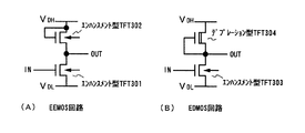
また、nチャネル型TFT203およびnチャネル型TFT204を組み合わせてNMOS回路を形成する場合、エンハンスメント型TFT同士で形成する場合(以下、EEMOS回路という)と、エンハンスメント型とデプレーション型とを組み合わせて形成する場合(以下、EDMOS回路という)がある。
【0040】
ここでEEMOS回路の例を図3(A)に、EDMOS回路の例を図3(B)に示す。図3(A)において、301、302はどちらもE型NTFTである。また、図3(B)において、303はE型NTFT、304はデプレーション型のnチャネル型TFT(以下、D型NTFTという)である。
【0041】
なお、図3(A)、(B)において、VDHは正の電圧が印加される電源線(正電源線)であり、VDLは負の電圧が印加される電源線(負電源線)である。負電源線は接地電位の電源線(接地電源線)としても良い。
【0042】
さらに、図3(A)に示したEEMOS回路もしくは図3(B)に示したEDMOS回路を用いてシフトレジスタを作製した例を図4に示す。図4において、400、401はフリップフロップ回路である。また、402、403はE型NTFTであり、E型NTFT402のゲートにはクロック信号(CL)が入力され、E型NTFT403のゲートには極性の反転したクロック信号(CLバー)が入力される。また、404で示される記号はインバータ回路であり、図4(B)に示すように、図3(A)に示したEEMOS回路もしくは図3(B)に示したEDMOS回路が用いられる。
【0043】
本発明の実施の形態では全てのTFTをnチャネル型TFTとすることによりpチャネル型TFTを形成する工程が削減されるため、EL発光装置の製造工程を簡略化することができる。また、それに伴って製造工程の歩留まりが向上し、EL発光装置の製造コストを下げることができる。
【0044】
【実施例】
〔実施例1〕
本実施例では、画素部とその周辺に設けられる駆動回路を同一の絶縁体上に製造する方法について説明する。但し、説明を簡単にするために、駆動回路に関してはnチャネル型TFTを組み合わせたNMOS回路を図示することとする。
【0045】
まず、図5(A)に示すように、プラスチックからなる絶縁体501を用意する。本実施例ではプラスチックからなる絶縁体501として、プラスチック基板501aの両面(表面および裏面)に保護膜(炭素膜、具体的にはダイヤモンドライクカーボン膜)501b、501cをコーティングした絶縁体を用意する。勿論、片面(表面もしくは裏面)に保護膜を設けた構成としても良い。
【0046】
次に絶縁体501上に下地膜502を300nmの厚さに形成する。本実施例では下地膜502として窒化酸化珪素膜をスパッタ法で積層して用いる。この時、絶縁体501に接する層の窒素濃度を10〜25wt%としておき、他の層よりも高めに窒素を含有させると良い。
【0047】
次に下地膜502の上に50nmの厚さの非晶質半導体膜(図示せず)をスパッタ法で形成する。絶縁体501がプラスチックであるため、成膜温度が200℃(好ましくは150℃)を超えないことが好ましい。
【0048】
なお、非晶質半導体膜に限定する必要はなく、非晶質構造を含む半導体膜(微結晶半導体膜を含む)であれば良い。非晶質半導体膜としては非晶質珪素もしくは非晶質シリコンゲルマニウム膜を用いることができる。また、膜厚は20〜100nmの厚さであれば良い。
【0049】
そして、公知のレーザー結晶化法を用いて非晶質珪素膜の結晶化を行い、結晶質半導体膜503を形成する。なお、本実施例では固体レーザー(具体的にはNd:YAGレーザーの第2高調波)を用いるが、エキシマレーザーを用いても良い。また、結晶化方法はプラスチックからなる絶縁体501の耐熱性が許す範囲であれば如何なる手段を用いても良い。
【0050】
次に、図5(B)に示すように、結晶質半導体膜503を1回目のフォトリソグラフィ工程によりエッチングして島状の半導体膜504〜507を形成する。これらは後にTFTの活性層となる半導体膜である。
【0051】
なお、本実施例ではTFTの活性層として結晶質半導体膜を用いているが、非晶質半導体膜を活性層として用いることも可能である。
【0052】
ここで本実施例では、半導体膜504〜507上に酸化珪素膜からなる保護膜(図示せず)を130nmの厚さにスパッタ法で形成し、半導体をp型半導体とする不純物元素(以下、p型不純物元素という)を半導体膜504〜507に添加する。p型不純物元素としては周期表の13族に属する元素(典型的にはボロンもしくはガリウム)を用いることができる。なお、この保護膜は不純物を添加する際に結晶質珪素膜が直接プラズマに曝されないようにするためと、微妙な濃度制御を可能にするために設ける。
【0053】
また、このとき添加されるp型不純物元素の濃度は、1×10¹⁵〜5×10¹⁷atoms/cm3(代表的には1×1016〜1×1017atoms/cm3)とすれば良い。この濃度で添加されたp型不純物元素はnチャネル型TFTのしきい値電圧の調節に用いられる。
【0054】
次に、半導体膜504〜507の表面を洗浄する。まず、オゾンを含む純水を用いて表面を洗浄する。その際、表面に薄い酸化膜が形成されるため、さらに1%に希釈したフッ酸水溶液を用いて薄い酸化膜を除去する。この処理により半導体膜504〜507の表面に付着した汚染物を除去できる。このときオゾンの濃度は6mg/L以上とすることが好ましい。これら一連の処理は大気開放することなく行われる。
【0055】
そして、半導体膜504〜507を覆ってゲート絶縁膜508をスパッタ法で形成する。ゲート絶縁膜508としては、10〜200nm、好ましくは50〜150nmの厚さの珪素を含む絶縁膜を用いれば良い。これは単層構造でも積層構造でも良い。本実施例では115nm厚の窒化酸化珪素膜を用いる。
【0056】
本実施例では、半導体膜504〜507の表面洗浄からゲート絶縁膜508の形成までを大気開放することなく行い、半導体膜504〜507とゲート絶縁膜508の界面における汚染物および界面準位の低減を図っている。この場合、洗浄室とスパッタ室とを少なくとも有したマルチチャンバー方式(もしくはインライン方式)の装置を用いれば良い。
【0057】
次に、第1の導電膜509として30nm厚の窒化タンタル膜を形成し、さらに第2の導電膜510として370nmのタングステン膜を形成する。他にも第1の導電膜としてタングステン膜、第2の導電膜としてアルミニウム合金膜を用いる組み合わせ、または第1の導電膜としてチタン膜、第2の導電膜としてタングステン膜を用いる組み合わせを用いても良い。
【0058】
これらの金属膜はスパッタ法で形成すれば良い。また、スパッタガスとしてXe、Ne等の不活性ガスを添加すると応力による膜はがれを防止することができる。また、タングステンターゲットの純度を99.9999%とすることで、抵抗率が20μΩcm以下の低抵抗なタングステン膜を形成することができる。
【0059】
また、前述の半導体膜504〜507の表面洗浄から第2の導電膜510の形成までを大気開放することなく行うことも可能である。この場合、洗浄室、絶縁膜を形成するスパッタ室および導電膜を形成するスパッタ室を少なくとも有したマルチチャンバー方式(もしくはインライン方式)の装置を用いれば良い。
【0060】
次に、レジストマスク511a〜511gを形成し、第1の導電膜509及び第2の導電膜510をエッチングする。なお、本明細書中ではここで行うエッチング処理を第1のエッチング処理と呼ぶ。(図5(C))
【0061】
本実施例では、ICP(Inductively Coupled Plasma:誘導結合型プラズマ)を用いたエッチング方法を採用する。
【0062】
まず、エッチングガスとして四フッ化炭素(CF4)ガス、塩素(Cl2)ガスおよび酸素(O2)ガスの混合ガスを用い、1Paの圧力とする。このとき各ガスの流量は、四フッ化炭素ガスが2.5×10⁻⁵m3/min、塩素ガスが2.5×10-5m3/min、酸素ガスが1.0×10-5m3/minである。
【0063】
そして、この状態でコイル型の電極に500WのRF電力(13.56MHz)を印加してプラズマを生成する。また、基板を乗せたステージには自己バイアス電圧として150WのRF電力(13.56MHz)を印加して、負の自己バイアスが基板に加わるようにする。このエッチング条件を第1のエッチング条件と呼ぶ。
【0064】
これにより第2の導電膜(タングステン膜)510が選択的にエッチングされる。これはエッチングガスに酸素が加わることで第1の導電膜(窒化タンタル膜)のエッチングの進行が極端に遅くなるためである。また、レジストマスク511a〜511eの後退を利用して15〜45°のテーパー角を有するテーパーを有する形状とすることができる。第1のエッチング条件では約25°のテーパー角を得ることができる。
【0065】
なお、テーパーとは、電極の端部における端面が斜めになった部分であり、下地との角度はテーパー角と呼ばれる。また、テーパーを有する形状とは電極端部があるテーパー角を持って斜めになった形状であり、台形はテーパーを有する形状に含まれる。
【0066】
次に、エッチングガスを四フッ化炭素ガスおよび塩素ガスの混合ガスにしてエッチングを行う。このとき圧力を1Pa、各ガスの流量は、四フッ化炭素ガスおよび塩素ガスともに3.0×10⁻⁵m3/minである。また、コイル型の電極には500WのRF電力を印加し、基板を乗せたステージには自己バイアス電圧として20WのRF電力を印加する。この条件を第2のエッチング条件と呼ぶ。
【0067】
こうして、第1の導電膜と第2の導電膜との積層膜からなるゲート電極512〜516並びにスイッチングTFTのソース配線517およびドレイン配線518が形成される。
【0068】
次に、ゲート電極512〜516、ソース配線517およびドレイン配線518をマスクとして自己整合的にn型不純物元素(本実施例ではリン)を添加する。こうして形成される不純物領域519〜527にはn型不純物元素が1×10²⁰〜1×10²¹atoms/cm3(代表的には2×1020〜5×1021atoms/cm3)の濃度で含まれる。これらの不純物領域519〜527はnチャネル型TFTのソース領域およびドレイン領域を形成する。
【0069】
次に、レジストマスク511a〜511gをそのまま用いてゲート電極のエッチングを行う。このエッチング条件は第1のエッチング条件において、自己バイアス電圧を20Wとしたエッチング条件とすれば良い。この条件では第2の導電膜(タングステン膜)のみが選択的にエッチングされ、第2の導電膜からなるゲート電極(以下、第2ゲート電極という)528〜532、第2の導電膜からなるソース配線(以下、第2ソース配線という)533および第2の導電膜からなるドレイン配線(以下、第2ドレイン配線という)534が形成される。(図5(D))
【0070】
次に、図5(E)に示すように、レジストマスク511a〜511gをそのまま用いて、n型不純物元素(本実施例ではリン)を添加する。この工程では第2ゲート電極528〜532がマスクとして機能し、n型不純物元素が2×10¹⁶〜5×10¹⁹atoms/cm3(代表的には5×1017〜5×1018atoms/cm3)の濃度で含まれたn型不純物領域535〜544が形成される。なお、本明細書ではこの濃度でn型不純物元素が添加された不純物領域をn型不純物領域(b)と呼ぶことにする。
【0071】
また、ここでの添加条件は、リンが第1の導電膜およびゲート絶縁膜を貫通して半導体膜に到達するよう加速電圧を70〜120kV(本実施例では90kV)と高めに設定する。
【0072】
次に、図6(A)に示すように、ゲート絶縁膜508をドライエッチング法によりエッチングし、互いに孤立したゲート絶縁膜545〜549を形成する。なお、本実施例ではn型不純物領域(a)519〜527が露呈するようにゲート絶縁膜をエッチングした例を示しているが、n型不純物領域(a)519〜527の表面にゲート絶縁膜が残っていても良い。
【0073】
このエッチング条件は、エッチングガスとしてCHF3(三フッ化炭素)ガスを3.5×10⁻⁵m3/minの流量で流し、エッチング圧力を7.3×103Paとする。また、印加電力は800Wとする。
【0074】
このとき、第1の導電膜(窒化タンタル膜)が同時にエッチングされ、第1の導電膜からなるゲート電極(以下、第1ゲート電極という)550〜554が形成される。従って、本実施例に示すEL発光装置は、第1ゲート電極と第2ゲート電極とを積層した構造のゲート電極を有する。
【0075】
また、図6(A)に示すように、第1ゲート電極550はn型不純物領域(b)535、536に一部が重なる(ゲート絶縁膜545を介して重なる)ことになる。即ち、n型不純物領域(b)535、536は第1ゲート電極550にゲート絶縁膜545を介して重なる領域535a、535bおよび第1ゲート電極550にゲート絶縁膜545を介して重ならない領域536a、536bを含むと言っても良い。
【0076】
なお、第1ゲート電極550はゲート電極の一部として機能するが、第1ゲート電極550にゲート絶縁膜545を介して重なった領域535a、536aはホットキャリア効果の低減に有効である。これによりホットキャリア効果に起因する劣化を抑制することができる。以上の特徴は全てのTFTに共通である。
【0077】
次に、図6(B)に示すように、添加されたn型不純物元素を活性化する。活性化手段としては、レーザーアニールが好ましい。勿論、プラスチック基板501aの耐熱性が許せば、ランプアニール、ファーネスアニールもしくはそれらとレーザーアニールを併用した手段を用いても良い。なお、このとき処理雰囲気中の酸素濃度を極力低くしておくことが望ましい。これはゲート電極の酸化を防ぐためであり、望ましくは酸素濃度を1ppm以下とする。
【0078】
次に、図6(C)に示すように、窒化珪素膜もしくは窒化酸化珪素膜からなる無機絶縁膜555を50〜200nmの厚さに形成する。この無機絶縁膜555はスパッタ法で形成すれば良い。
【0079】
その後、水素(H2)ガスもしくはアンモニア(NH3)ガスを用いたプラズマ処理により水素化処理を行う。水素化処理が終了したら、有機絶縁膜556として可視光を透過する樹脂膜を1〜2μmの厚さに形成する。樹脂膜としては、ポリイミド膜、ポリアミド膜、アクリル樹脂膜もしくはBCB(ベンゾシクロブテン)膜を用いれば良い。また、感光性樹脂膜を用いることも可能である。
【0080】
なお、本実施例では無機絶縁膜555および有機絶縁膜556の積層膜を層間絶縁膜と呼ぶ。
【0081】
次に、図6(D)に示すように、層間絶縁膜に対してコンタクトホールを形成し、配線557〜562および画素電極563を形成する。なお、本実施例ではこの配線を、下層側から50nmのチタン膜、200nmのチタンを含むアルミニウム膜、200nmのリチウムを含むアルミニウム膜をスパッタ法で連続形成した三層構造の積層膜とする。また、リチウムを含むアルミニウム膜のみ蒸着法で形成することもできる。但し、その場合においても大気開放しないで連続形成することが望ましい。
【0082】
ここで画素電極563の最表面が仕事関数の小さい金属面となるようにすることは重要である。これは画素電極563がそのままEL素子の陰極として機能することになるからである。そのため、少なくとも画素電極563の最表面は周期表の1族もしくは2族に属する元素を含む金属膜またはビスマス(Bi)膜とすることが好ましい。また、配線557〜562は画素電極563と同時に形成されるため、同一の導電膜で形成されることになる。
【0083】
このとき、配線557、559はNMOS回路のソース配線、558はドレイン配線として機能する。また、配線560はソース配線517とスイッチングTFTのソース領域とを電気的に接続する配線として機能し、配線561はドレイン配線518とスイッチングTFTのドレイン領域とを電気的に接続する配線として機能する。また、562は電流制御TFTのソース配線(電流供給線に相当する)であり、563は電流制御TFTの画素電極である。
【0084】
次に、図7に示すように画素電極563の端部を覆う絶縁膜(以下、バンクという)564を形成する。バンク564は100〜400nmの珪素を含む絶縁膜もしくは有機樹脂膜をパターニングして形成すれば良い。このバンク564は画素と画素との間(画素電極と画素電極との間)を埋めるように形成される。また、次に形成する発光層等の有機EL膜が画素電極563の端部に直接触れないようにする目的もある。
【0085】
なお、バンク564は絶縁膜であるため、成膜時における素子の静電破壊には注意が必要である。本実施例ではバンク564の材料となる絶縁膜中にカーボン粒子や金属粒子を添加して抵抗率を下げ、静電気の発生を抑制する。この際、抵抗率は1×10⁶〜1×10¹²Ωm(好ましくは1×10⁸〜1×10¹⁰Ωm)となるようにカーボン粒子や金属粒子の添加量を調節すれば良い。
【0086】
次に、EL層565を蒸着法により形成する。なお、本実施例では、正孔注入層および発光層の積層体をEL層と呼んでいる。即ち、発光層に対して正孔注入層、正孔輸送層、正孔阻止層、電子輸送層、電子注入層もしくは電子阻止層を組み合わせた積層体をEL層と定義する。なお、これらは有機材料であっても無機材料であっても良いし、高分子であっても低分子であっても良い。
【0087】
本実施例では、まず電子注入層としてフッ化リチウム(LiF)膜を20nmの厚さに成膜し、さらに発光層としてアルミキノリラト錯体(Alq3)を80nmの厚さに形成する。また、発光層に対して発光中心となるドーパント(代表的には蛍光色素)を共蒸着により添加しても良い。このドーパントとして、三重項励起を経由して発光する有機材料を用いても良い。
【0088】
次に、EL層565を形成したら、仕事関数が大きく、可視光に対して透明な酸化物導電膜からなる陽極566を300nmの厚さに形成する。本実施例では、酸化亜鉛に酸化ガリウムを添加した酸化物導電膜を蒸着法を用いて形成する。また、他の酸化物導電膜として、酸化インジウム、酸化亜鉛、酸化スズ、もしくはそれらを組み合わせた化合物からなる酸化物導電膜を用いることも可能である。こうして画素電極(陰極)563、EL層565および陽極566を含むEL素子567が形成される。
【0089】
なお、陽極566を形成した後、EL素子567を完全に覆うようにしてパッシベーション膜568を設けることは有効である。パッシベーション膜568としては、炭素膜、窒化珪素膜もしくは窒化酸化珪素膜を含む絶縁膜からなり、該絶縁膜を単層もしくは組み合わせた積層で用いる。
【0090】
この際、カバレッジの良い膜をパッシベーション膜として用いることが好ましく、炭素膜、特にDLC(ダイヤモンドライクカーボン)膜を用いることは有効である。DLC膜は室温から100℃以下の温度範囲で成膜可能であるため、耐熱性の低いEL層565の上方にも容易に成膜することができる。また、DLC膜は酸素に対するブロッキング効果が高く、EL層565の酸化を抑制することが可能である。そのため、この後に続く封止工程を行う間にEL層565が酸化するといった問題を防止できる。
【0091】
さらに、パッシベーション膜568上に封止材569を設け、カバー材570を貼り合わせる。封止材569としては紫外線硬化樹脂を用いれば良く、内部に吸湿効果を有する物質もしくは酸化防止効果を有する物質を設けることは有効である。また、本実施例においてカバー材570はプラスチック基板(プラスチックフィルムも含む)570aの両面に炭素膜(好ましくはダイヤモンドライクカーボン膜)570b、570cを用いる。
【0092】
こうして図7に示すような構造のEL発光装置が完成する。なお、バンク564を形成した後、パッシベーション膜568を形成するまでの工程をマルチチャンバー方式(またはインライン方式)の成膜装置を用いて、大気解放せずに連続的に処理することは有効である。また、さらに発展させてカバー材570を貼り合わせる工程までを大気解放せずに連続的に処理することも可能である。
【0093】
こうして、プラスチック基板を母体とする絶縁体501上にnチャネル型TFT601、602、スイッチングTFT(nチャネル型TFT)603および電流制御TFT(nチャネル型TFT)604が形成される。ここまの製造工程で必要としたフォトリソグラフィ工程は5回であり、一般的なアクティブマトリクス型EL発光装置よりも少ない。
【0094】
即ち、TFTの製造工程が大幅に簡略化されており、歩留まりの向上および製造コストの低減が実現できる。また、TFTおよびEL素子がプラスチック基板を母体とする絶縁体(カバー材も含む)で挟まれた構造となったおり、非常にフレキシブルで軽量なEL発光装置をも実現できる。
【0095】
さらに、図6(A)を用いて説明したように、第1ゲート電極にゲート絶縁膜を介して重なる不純物領域を設けることによりホットキャリア効果に起因する劣化に強いnチャネル型TFTを形成することができる。そのため、信頼性の高いEL発光装置を実現できる。
【0096】
また、本実施例のEL発光装置の回路構成例を図8に示す。なお、本実施例ではデジタル駆動を行うための回路構成を示す。本実施例では、ソース側駆動回路801、画素部806及びゲート側駆動回路807を有している。なお、本明細書中において、駆動回路とはソース側駆動回路およびゲート側駆動回路を含めた総称である。
【0097】
ソース側駆動回路801は、シフトレジスタ802、ラッチ(A)803、ラッチ(B)804、バッファ805を設けている。なお、アナログ駆動の場合はラッチ(A)、(B)の代わりにサンプリング回路(トランスファゲートもしくはアナログスイッチともいう)を設ければ良い。また、ゲート側駆動回路807は、シフトレジスタ808、バッファ809を設けている。なお、シフトレジスタ802、808としては図4に示したシフトレジスタを用いれば良い。
【0098】
また、本実施例において、画素部806は複数の画素を含み、その複数の画素にEL素子が設けられている。このとき、EL素子の陰極は電流制御TFTのドレインに電気的に接続されていることが好ましい。
【0099】
これらソース側駆動回路801およびゲート側駆動回路807は全てnチャネル型TFTで形成され、全ての回路は図3(A)に示したEEMOS回路を基本単位として形成されている。従来のCMOS回路に比べると消費電力は若干上がってしまうが、もともとCMOS回路を駆動回路に用いたEL発光装置は95%近くの電力が画素部で消費されているので、多少NMOS回路を用いることで駆動回路の消費電力が上がったとしてもさほど問題とはならない。
【0100】
なお、図示していないが、画素部806を挟んでゲート側駆動回路807の反対側にさらにゲート側駆動回路を設けても良い。この場合、双方は同じ構造でゲート配線を共有しており、片方が壊れても残った方からゲート信号を送って画素部を正常に動作させるような構成とする。
【0101】
なお、上記構成は、図5〜図7に示した製造工程に従ってTFTを作製することによって実現することができる。また、本実施例では画素部と駆動回路の構成のみ示しているが、本実施例の製造工程に従えば、その他にも信号分割回路、D/Aコンバータ、オペアンプ、γ補正回路などの論理回路を同一の絶縁体上に形成可能であり、さらにはメモリやマイクロプロセッサをも形成しうる。
【0102】
さらに、EL素子を保護するための封止(または封入)工程まで行った後の本実施例のEL発光装置について図9(A)、(B)を用いて説明する。なお、必要に応じて図5〜図8で用いた符号を引用する。
【0103】
図9(A)は、EL素子の封止までを行った状態を示す上面図、図9(B)は図9(A)をA−A’で切断した断面図である。点線で示された801はソース側駆動回路、806は画素部、807はゲート側駆動回路である。また、901はカバー材、902は第1シール材、903は第2シール材であり、第1シール材902で囲まれた内側には封止材907が設けられる。
【0104】
なお、904はソース側駆動回路801及びゲート側駆動回路807に入力される信号を伝送するための配線であり、外部入力端子となるFPC(フレキシブルプリントサーキット)905からビデオ信号やクロック信号を受け取る。なお、ここではFPCしか図示されていないが、このFPCにはプリント配線基盤(PWB)が取り付けられていても良いし、TCP(Tape Carrier Package)の形態となっていても良い。また、COG(Chip On Glass)によりICを基板上に実装しても良い。
【0105】
本明細書におけるEL発光装置には、EL発光装置本体だけでなく、それにFPC、TCPもしくはPWBが取り付けられた状態をも含むものとする。
【0106】
次に、断面構造について図9(B)を用いて説明する。絶縁体501の上方には画素部806、ゲート側駆動回路807が形成されており、画素部806は電流制御用TFT604とそのドレインに電気的に接続された画素電極563を含む複数の画素により形成される。また、ゲート側駆動回路807はnチャネル型TFT601とnチャネル型TFT602とを組み合わせたNMOS回路(図3参照)を用いて形成される。
【0107】
画素電極563はEL素子の陰極として機能する。また、画素電極563の両端にはバンク564が形成され、画素電極563上にはEL層565およびEL素子の陽極566が形成される。陽極566は全画素に共通の配線としても機能し、接続配線904を経由してFPC905に電気的に接続されている。さらに、画素部806及びゲート側駆動回路807に含まれる素子は全て陽極566およびパッシベーション膜567で覆われている。
【0108】
また、第1シール材902によりカバー材901が貼り合わされている。なお、カバー材901とEL素子との間隔を確保するために樹脂膜からなるスペーサを設けても良い。そして、第1シール材902の内側には封止材907が充填されている。なお、第1シール材902、封止材907としてはエポキシ系樹脂を用いるのが好ましい。また、第1シール材902はできるだけ水分や酸素を透過しない材料であることが望ましい。さらに、封止材907の内部に吸湿効果をもつ物質や酸化防止効果をもつ物質を含有させても良い。
【0109】
EL素子を覆うようにして設けられた封止材907はカバー材901を接着するための接着剤としても機能する。また、本実施例ではカバー材901を構成するプラスチック基板901aの材料としてFRP(Fiberglass-Reinforced Plastics)、PVF(ポリビニルフロライド)、マイラー、ポリエステルまたはアクリルを用いることができる。
【0110】
さらに本実施例ではプラスチック基板901aの両面に保護膜として炭素膜(具体的にはダイヤモンドライクカーボン膜)901b、901cを2〜30nmの厚さに設けている。このような炭素膜は、酸素および水の侵入を防ぐとともにプラスチック基板901aの表面を機械的に保護する役割をもつ。また、外側の炭素膜901bに偏光板(代表的には円偏光板)を貼り付けることも可能である。
【0111】
また、封止材907を用いてカバー材901を接着した後、封止材907の側面(露呈面)を覆うように第2シール材903を設ける。第2シール材903は第1シール材902と同じ材料を用いることができる。
【0112】
以上のような構造でEL素子を封止材907に封入することにより、EL素子を外部から完全に遮断することができ、外部から水分や酸素等のEL層の酸化による劣化を促す物質が侵入することを防ぐことができる。従って、信頼性の高いEL発光装置が得られる。
【0113】
〔実施例2〕
本実施例では、実施例1に示したEL発光装置とは異なる構造でEL素子を封止した例について図10(A)、(B)を用いて説明する。なお、図9と同一の部分については同一の符号を用いる。また、図10(B)は図10(A)をA−A’で切断した断面図である。
【0114】
まず、本実施例ではTFTおよびEL素子を形成する絶縁体1001としてプラスチックフィルム1001aの両面を保護膜として炭素膜(具体的にはダイヤモンドライクカーボン膜)1001b、1001cでコーティング(被覆)したものを用いる。なお、プラスチックフィルム1001aの両面に炭素膜1001b、1001cを成膜する歳はロールトゥロール方式を用いれば良い。
【0115】
また、実施例1に従ってEL素子まで作製した基板に、封止材907を用いてカバー材1002を貼り合わせる。カバー材1002としてもプラスチックフィルム1002aの両面を保護膜として炭素膜(具体的にはダイヤモンドライクカーボン膜)1002b、1002cでコーティングしたものを用いる。さらに、カバー材1002の端面(端部)は第2シール材1003により封止する。
【0116】
〔実施例3〕
本実施例では、実施例1においてnチャネル型TFT601をデプレーション型とし、nチャネル型TFT602、スイッチングTFT603および電流制御TFT604をエンハンスメント型とする場合について説明する。
【0117】
まず、実施例1に従って図5(A)の状態を得る。次に、スパッタ法で100〜150nmの酸化珪素膜1101を成膜し、その上にnチャネル型TFT601となる領域にレジストマスク1102を形成する。(図11(A))
【0118】
次に、レジストマスク1102を用いて結晶質半導体膜503に周期表の13族に属する元素(本実施例ではボロン)を添加する。こうして1×10¹⁵〜5×10¹⁷atoms/cm3(代表的には1×1016〜1×1017atoms/cm3)の濃度でボロンが添加された領域1103およびボロンが添加されなかった領域1104が形成される。(図11(B))
【0119】
次に、結晶質半導体膜をパターニングして、島状の半導体膜1105〜1108を形成する。このとき、半導体膜1105はボロンが添加されなかった領域1104で形成され、半導体膜1106〜1108はボロンが添加された領域で形成される。即ち、半導体膜1105を活性層とするTFTはチャネル形成領域にボロンは含まれない、もしくは含まれていても5×10¹⁴atoms/cm3以下であり、半導体膜1106〜1108を活性層とするTFTはチャネル形成領域にボロンが1×1015〜5×1017atoms/cm3(代表的には1×1016〜1×1017atoms/cm3)の濃度で含まれている。(図11(C))
【0120】
この後の工程は、実施例1に従えば良い。本実施例の場合、半導体膜1105を用いて形成されたnチャネル型TFTはデプレーション型TFT(即ちノーマリオンのnチャネル型TFT)となり、半導体膜1106〜1108を用いて形成されたnチャネル型TFTはエンハンスメント型TFT(即ちノーマリオフのnチャネル型TFT)となる。
【0121】
本実施例を実施した場合、上記方法で形成されたデプレーション型TFTおよびエンハンスメント型TFTを組み合わせて、図3(B)に示したEDMOS回路を形成することができる。
【0122】
なお、本実施例ではボロンを半導体膜に添加することによってしきい値電圧を正の方向にシフトさせ、ボロンの添加されたチャネル形成領域を含むTFTをエンハンスメント型とする例を示したが、周期表の15族に属する元素(代表的にはリンもしくは砒素)を半導体膜に添加することによってしきい値電圧を負の方向にシフトさせ、周期表の15族に属する元素の添加されたチャネル形成領域を含むTFTをデプレーション型とすることも可能である。
【0123】
なお、本実施例は実施例1もしくは実施例2と組み合わせて実施することが可能である。
【0124】
〔実施例4〕
本実施例では、ソース側駆動回路およびゲート側駆動回路を全てE型NTFTで形成した場合について図12〜図14を用いて説明する。本発明ではシフトレジスタの代わりにnチャネル型TFTのみを用いたデコーダを用いる。
【0125】
図12はゲート側駆動回路の例である。図12において、100がゲート側駆動回路のデコーダ、101がゲート側駆動回路のバッファ部である。なお、バッファ部とは複数のバッファ(緩衝増幅器)が集積化された部分を指す。また、バッファとは後段の影響を前段に与えずに駆動を行う回路を指す。
【0126】
まずゲート側デコーダ100を説明する。まず102はデコーダ100の入力信号線(以下、選択線という)であり、ここではA1、A1バー(A1の極性が反転した信号)、A2、A2バー(A2の極性が反転した信号)、…An、Anバー(Anの極性が反転した信号)を示している。即ち、2n本の選択線が並んでいると考えれば良い。
【0127】
選択線の本数はゲート側駆動回路から出力されるゲート配線が何列あるかによってその数が決まる。例えばVGA表示の画素部をもつ場合はゲート配線が480本となるため、9bit分(n=9に相当する)で合計18本の選択線が必要となる。選択線102は図13のタイミングチャートに示す信号を伝送する。図13に示すように、A1の周波数を1とすると、A2の周波数は2-1倍、A3の周波数は2-2倍、Anの周波数は2-(n-1)倍となる。
【0128】
また、103aは第1段のNAND回路(NANDセルともいう)、103bは第2段のNAND回路、103cは第n段のNAND回路である。NAND回路はゲート配線の本数分が必要であり、ここではn個が必要となる。即ち、本発明ではデコーダ100が複数のNAND回路からなる。
【0129】
また、NAND回路103a〜103cは、nチャネル型TFT104〜109が組み合わされてNAND回路を形成している。なお、実際には2n個のTFTがNAND回路103に用いられている。また、nチャネル型TFT104〜109の各々のゲートは選択線102(A1、A1バー、A2、A2バー…An、Anバー)のいずれかに接続されている。
【0130】
このとき、NAND回路103aにおいて、A1、A2…An(これらを正の選択線と呼ぶ)のいずれかに接続されたゲートを有するnチャネル型TFT104〜106は、互いに並列に接続されており、共通のソースとして負電源線(VDL)110に接続され、共通のドレインとして出力線71に接続されている。また、A1バー、A2バー…Anバー(これらを負の選択線と呼ぶ)のいずれかに接続されたゲートを有するnチャネル型TFT107〜109は、互いに直列に接続されており、回路端に位置するnチャネル型TFT109のソースが正電源線(VDH)112に接続され、もう一方の回路端に位置するnチャネル型TFT107のドレインが出力線111に接続されている。
【0131】
以上のように、本発明においてNAND回路は直列に接続されたn個のnチャネル型TFTおよび並列に接続されたn個のnチャネル型TFTを含む。但し、n個のNAND回路103a〜103cにおいて、nチャネル型TFTと選択線との組み合わせはすべて異なる。即ち、出力線111は必ず1本しか選択されないようになっており、選択線102には出力線111が端から順番に選択されていくような信号が入力される。
【0132】
次に、バッファ部101はNAND回路103a〜103cの各々に対応して複数のバッファ113a〜113cにより形成されている。但しバッファ113a〜113cはいずれも同一構造で良い。
【0133】
また、バッファ113a〜113cはnチャネル型TFT114〜116を用いて形成される。デコーダからの出力線111はnチャネル型TFT114(第1のnチャネル型TFT)のゲートとして入力される。nチャネル型TFT114は正電源線(VDH)117をソースとし、画素部に続くゲート配線118をドレインとする。また、nチャネル型TFT115(第2のnチャネル型TFT)は正電源線(VDH)117をゲートとし、負電源線(VDL)119をソースとし、ゲート配線118をドレインとして常時オン状態となっている。
【0134】
即ち、本発明において、バッファ113a〜113cは第1のnチャネル型TFT(nチャネル型TFT114)および第1のnチャネル型TFTに直列に接続され、且つ、第1のnチャネル型TFTのドレインをゲートとする第2のnチャネル型TFT(nチャネル型TFT115)を含む。
【0135】
また、nチャネル型TFT116(第3のnチャネル型TFT)はリセット信号線(Reset)をゲートとし、負電源線(VDL)119をソースとし、ゲート配線118をドレインとする。なお、負電源線(VDL)119は接地電源線(GND)としても構わない。
【0136】
このとき、nチャネル型TFT115のチャネル幅(W1とする)とnチャネル型TFT114のチャネル幅(W2とする)との間にはW1<W2の関係がある。なお、チャネル幅とはチャネル長に垂直な方向におけるチャネル形成領域の長さである。
【0137】
バッファ113aの動作は次の通りである。まず出力線111に負電圧が加えられているとき、nチャネル型TFT114はオフ状態(チャネルが形成されていない状態)となる。一方でnチャネル型TFT115は常にオン状態(チャネルが形成されている状態)であるため、ゲート配線118には負電源線119の電圧が加えられる。
【0138】
ところが、出力線111に正電圧が加えられた場合、nチャネル型TFT114がオン状態となる。このとき、nチャネル型TFT114のチャネル幅がnチャネル型TFT115のチャネル幅よりも大きいため、ゲート配線118の電位はnチャネル型TFT114側の出力に引っ張られ、結果的に正電源線117の電圧がゲート配線118に加えられる。
【0139】
従って、ゲート配線118は、出力線111に正電圧が加えられるときは正電圧(画素のスイッチング素子として用いるnチャネル型TFTがオン状態になるような電圧)を出力し、出力線111に負電圧が加えられているときは常に負電圧(画素のスイッチング素子として用いるnチャネル型TFTがオフ状態になるような電圧)を出力する。
【0140】
なお、nチャネル型TFT116は正電圧が加えられたゲート配線118を強制的に負電圧に引き下げるリセットスイッチとして用いられる。即ち、ゲート配線118の選択期間が終了したら。リセット信号を入力してゲート配線118に負電圧を加える。但しnチャネル型TFT116は省略することもできる。
【0141】
以上のような動作のゲート側駆動回路によりゲート配線が順番に選択されることになる。次に、ソース側駆動回路の構成を図14に示す。図14に示すソース側駆動回路はデコーダ121、ラッチ122およびバッファ部123を含む。なお、デコーダ121およびバッファ部123の構成はゲート側駆動回路と同様であるので、ここでの説明は省略する。
【0142】
図14に示すソース側駆動回路の場合、ラッチ122は第1段目のラッチ124および第2段目のラッチ125からなる。また、第1段目のラッチ124および第2段目のラッチ125は、各々m個のnチャネル型TFT126a〜126cで形成される複数の単位ユニット127a及び127bを有する。デコーダ121からの出力線128は単位ユニット127aを形成するm個のnチャネル型TFT126a〜126cのゲートに入力される。なお、mは任意の整数である。
【0143】
例えば、VGA表示の場合、ソース配線の本数は640本である。m=1の場合はNAND回路も640個必要となり、選択線は20本(10bit分に相当する)必要となる。しかし、m=8とすると必要なNAND回路は80個となり、必要な選択線は14本(7bit分に相当する)となる。即ち、ソース配線の本数をM本とすると、必要なNAND回路は(M/m)個となる。
【0144】
そして、nチャネル型TFT126a〜126cのソースは各々ビデオ信号線(V1、V2…Vk)129に接続される。即ち、出力線128に正電圧が加えられると一斉にnチャネル型TFT126a〜126cがオン状態となり、各々に対応するビデオ信号が取り込まれる。また、こうして取り込まれたビデオ信号は、nチャネル型TFT126a〜126cの各々に接続されたコンデンサ130a〜130cに保持される。
【0145】
また、第2段目のラッチ125も複数の単位ユニット127bを有し、単位ユニット127bはm個のnチャネル型TFT131a〜131cで形成される。nチャネル型TFT131a〜131cのゲートはすべてラッチ信号線132に接続され、ラッチ信号線132に負電圧が加えられると一斉にnチャネル型TFT131a〜131cがオン状態となる。
【0146】
その結果、コンデンサ130a〜130cに保持されていた信号が、nチャネル型TFT131a〜131cの各々に接続されたコンデンサ133a〜133cに保持されると同時にバッファ123へと出力される。そして、図13で説明したようにバッファを介してソース配線134に出力される。以上のような動作のソース側駆動回路によりソース配線が順番に選択されることになる。
【0147】
以上のように、nチャネル型TFTのみでゲート側駆動回路およびソース側駆動回路を形成することにより画素部および駆動回路をすべてnチャネル型TFTで形成することが可能となる。なお、ソース側駆動回路もしくはゲート側駆動回路のいずれか片方を外付けのIC(典型的にはTCPもしくはCOG)とする場合にも本発明は実施できる。
【0148】
〔実施例5〕
本実施例では、ソース側駆動回路およびゲート側駆動回路をE型NTFT(E型NTFT)およびD型NTFT(D型NTFT)を組み合わせて形成した場合について図15、図16を用いて説明する。
【0149】
図15はゲート側駆動回路の例である。図15において、140がシフトレジスタ、141がNAND回路部、142がバッファ部である。
【0150】
ここでシフトレジスタ140は図4に示したシフトレジスタを具体的に図示したものである。まず143はクロック信号線、144は極性が反転したクロック信号線、145は正電源線(VDH)、146は接地電源線(GND)である。そして、本実施例ではシフトレジスタ140を形成する基本単位として三つのフリップフロップ回路147a〜147cが図示されている。なお、実際には複数のフリップフロップ回路が直列に接続されてシフトレジスタ140を形成している。
【0151】
また、本実施例においてフリップフロップ回路147aは図4に示したフリップフロップ回路400に対応し、フリップフロップ回路147bはフリップフロップ回路401に対応した回路構成となっている。また、フリップフロップ回路147a〜147cはE型NTFTおよびD型NTFTで形成される。
【0152】
フリップフロップ回路147aにおいて、148はE型NTFTでゲートはクロック信号線143に接続されている。また、図3(B)の構造のEDMOS回路148a〜148cが図4に示すような配置で形成される。なお、150は正電源線(VDH)であり、151は接地電源線(GND)である。
【0153】
また、フリップフロップ回路147bはE型NTFT152のゲートが、極性が反転したクロック信号線144に接続されている点を除けばフリップフロップ回路147aと同じ回路構成である。
【0154】
そして、フリップフロップ回路147aの出力線153およびフリップフロップ回路147bの出力線154はNAND回路155aに接続される。なお、NAND回路部141には三つのNAND回路155a〜155cが図示されているが、実際には複数のNAND回路からなる。NAND回路は二つのフリップフロップ回路に一つに割合で配置されている。また、NAND回路155a〜155cはE型NTFTおよびD型NTFTで形成される。
【0155】
NAND回路155aにおいて、E型NTFT156のゲートには出力線153が接続され、ソースには接地電源線151が接続され、ドレインにはE型NTFT157が接続される。また、E型NTFT157のゲートには出力線154が接続され、ソースにはE型NTFT156のドレインが接続され、ドレインには出力線158が接続される。また、D型NTFT159のソースは正電源線160に接続され、ゲートおよびドレインは出力線158に接続される。
【0156】
そして、NAND回路155aの出力線158はEDMOS回路(インバータ回路と呼んでも良い)161aに接続される。なお、バッファ部142には三つのEDMOS回路161a〜161cが図示されているが、実際には複数のEDMOS回路からなる。
【0157】
EDMOS回路161aにおいて、E型NTFT162のゲートは出力線158に接続され、ソースは負電源線(VDL)163に接続され、ドレインは出力線(画素部のゲート配線に相当する)164に接続される。また、D型NTFT165のゲートおよびドレインは出力線164に接続され、ソースは正電源線160に接続される。
【0158】
次に、ソース側駆動回路の構成を図16に示す。図16に示すソース側駆動回路は図15に示したゲート側駆動回路にトランスファゲート165a〜165cを付け加えた構成となっており、シフトレジスタ140、NAND回路部141およびバッファ部142は同じ回路を用いることができる。なお、この構成はアナログ駆動を行う場合の構成である。
【0159】
また、本実施例ではトランスファゲート165a〜165cとしてE型NTFTを並列に二つ設けているが、これは冗長設計であると同時に電流の供給能力を稼ぐための工夫である。また、166はビデオ信号線である。
【0160】
ところで、本実施例においてデジタル駆動を行う場合、図14にて説明したラッチ122およびバッファ部123をNAND回路部141の下に設ければ良い。また、逆に実施例4において、図14に示したソース側駆動回路をアナログ駆動に対応させるにはラッチ122を省略し、バッファ部123の後段に図16に示したトランスファゲートを設ければ良い。
【0161】
以上のように、nチャネル型TFTのみでゲート側駆動回路およびソース側駆動回路を形成することにより画素部および駆動回路をすべてnチャネル型TFTで形成することが可能となる。なお、ソース側駆動回路もしくはゲート側駆動回路のいずれか片方を外付けのICチップとする場合にも本発明は実施できる。
【0162】
〔実施例6〕
本実施例では、本発明のEL発光装置における画素構造の一例を図17に示す。図17(A)において、1701はゲート配線、1702はソース配線、1703は正電源線、1704は負電源線(接地電源線としても良い)である。また、1705〜1708はE型NTFT、1709、1710はD型NTFTである。また、1711はEL素子であり、E型NTFT1708に接続される。
【0163】
本実施例の画素構造は、一画素の中に6個のTFTを設け、SRAM(スタティックランダムアクセスメモリ)を形成している。具体的には複数のE型NTFTおよび複数のD型NTFTでSRAMを形成している。このように本発明を実施するにあたって一画素に含まれるTFTの個数に限定はない。
【0164】
なお、本実施例の画素構造の場合、E型NTFT1705がスイッチングTFTとして機能し、E型NTFT1708が電流制御TFTとして機能する。また、E型NTFT1706およびD型NTFT1709からなるインバータ回路とE型NTFT1707およびD型NTFT1710からなるインバータ回路とを組み合わせてメモリ機能を持たせている。
【0165】
さらに、図17(B)は図17(A)に示した隣接する二つの画素を負電源線1704を共通化して対称に配置した例である。これにより画素部に設ける配線の本数を低減することができ、画素の高密度化が図れる。
【0166】
なお、本実施例の構成は、実施例1〜実施例5のいずれの構成とも組み合わせて実施することが可能である。
【0167】
〔実施例7〕
実施例4もしくは実施例5に示したソース側駆動回路およびゲート側駆動回路は、液晶表示装置に用いることも可能である。即ち、図3(A)に示したEEMOS回路、図3(B)に示したEDMOS回路、図4に示したシフトレジスタ、図13に示したゲート側駆動回路もしくは図14に示したソース側駆動回路はいずれも液晶表示装置の駆動回路として用いることが可能である。
【0168】
なお、液晶表示装置とは液晶パネルにFPC(フレキシブルプリントサーキット)が取り付けられた液晶モジュールを指す。なお、液晶モジュールにはFPCの先にPWB(プリント配線基盤)が設けられている場合も含むものとする。また、FPCにICを取り付けたTCP(Tape Carrier Package)の形態となっていても良い。また、COG(Chip On Glass)によりICを基板上に実装しても良い。
【0169】
〔実施例8〕
本発明を実施するにあたって、TFTとしてはトップゲート型TFT(代表的にはプレーナ型TFT)だけでなく、ボトムゲート型TFT(代表的には逆スタガ型TFT)を用いても良い。また、半導体基板(代表的にはシリコン基板)に形成したMOSFETを用いることも可能である。
【0170】
なお、本実施例の構成は実施例1〜実施例7のいずれに含まれた構成とも組み合わせて実施することが可能である。
【0171】
〔実施例9〕
本発明を実施して形成された発光装置もしくは液晶表示装置は様々な電気器具の表示部として用いることができる。本発明の電気器具としては、ビデオカメラ、デジタルカメラ、ゴーグル型ディスプレイ(ヘッドマウントディスプレイ)、カーナビゲーションシステム、カーオーディオ、ノート型パーソナルコンピュータ、ゲーム機器、携帯情報機器(モバイルコンピュータ、携帯電話、携帯型ゲーム機または電子書籍)、記録媒体を備えた画像再生装置などが挙げられる。それら電気器具の具体例を図20、図21に示す。
【0172】
図20(A)はELディスプレイであり、筐体2001、支持台2002、表示部2003を含む。本発明の発光装置もしくは液晶表示装置は表示部2003に用いることができる。表示部2003にEL発光装置を用いる場合、自発光型であるためバックライトが必要なく薄い表示部とすることができる。
【0173】
図20(B)はビデオカメラであり、本体2101、表示部2102、音声入力部2103、操作スイッチ2104、バッテリー2105、受像部2106を含む。本発明の発光装置もしくは液晶表示装置は表示部2102に用いることができる。
【0174】
図20(C)はデジタルカメラであり、本体2201、表示部2202、接眼部2203、操作スイッチ2204を含む。本発明の発光装置もしくは液晶表示装置は表示部2202に用いることができる。
【0175】
図20(D)は記録媒体を備えた画像再生装置(具体的にはDVD再生装置)であり、本体2301、記録媒体(CD、LDまたはDVD等)2302、操作スイッチ2303、表示部(a)2304、表示部(b)2305を含む。表示部(a)は主として画像情報を表示し、表示部(b)は主として文字情報を表示するが、本発明の発光装置もしくは液晶表示装置はこれら表示部(a)、(b)に用いることができる。なお、記録媒体を備えた画像再生装置には、CD再生装置、ゲーム機器なども含まれうる。
【0176】
図20(E)は携帯型(モバイル)コンピュータであり、本体2401、表示部2402、受像部2403、操作スイッチ2404、メモリスロット2405を含む。本発明の発光装置もしくは液晶表示装置は表示部2402に用いることができる。この携帯型コンピュータはフラッシュメモリや不揮発性メモリを集積化した記録媒体に情報を記録したり、それを再生したりすることができる。
【0177】
図20(F)はパーソナルコンピュータであり、本体2501、筐体2502、表示部2503、キーボード2504を含む。本発明の発光装置もしくは液晶表示装置は表示部2503に用いることができる。
【0178】
また、上記電気器具はインターネットやCATV(ケーブルテレビ)などの電子通信回線を通じて配信された情報を表示することが多くなり、特に動画情報を表示する機会が増してきている。表示部にEL発光装置を用いた場合、EL発光装置の応答速度が非常に高いため遅れのない動画表示が可能となる。
【0179】
また、EL発光装置は発光している部分が電力を消費するため、発光部分が極力少なくなるように情報を表示することが望ましい。従って、携帯情報端末、特に携帯電話やカーオーディオのような文字情報を主とする表示部にEL発光装置を用いる場合には、非発光部分を背景として文字情報を発光部分で形成するように駆動することが望ましい。
【0180】
ここで図21(A)は携帯電話であり、キー操作を行う部位(操作部)2601、情報表示を行う部位(情報表示部)2602であり、操作部2601および情報表示部2602は連結部2603で連結している。また、操作部2601には音声入力部2604、操作キー2605が設けられ、情報表示部2602には音声出力部2606、表示部2607が設けられている。
【0181】
本発明の発光装置もしくは液晶表示装置は表示部2607に用いることができる。なお、表示部2607にEL発光装置を用いる場合、黒色の背景に白色の文字を表示することで携帯電話の消費電力を抑えることができる。
【0182】
図21(A)に示した携帯電話の場合、表示部2604に用いたEL発光装置にNMOS回路でセンサ(NMOSセンサ)を内蔵させ、指紋もしくは手相を読みとることで使用者を認証する認証システム用端末として用いることもできる。また、外部の明るさ(照度)を読みとり、設定されたコントラストで情報表示が可能となるように発光させることもできる。
【0183】
さらに、操作スイッチ2605を使用している時に輝度を下げ、操作スイッチの使用が終わったら輝度を上げることで低消費電力化することができる。また、着信した時に表示部2604の輝度を上げ、通話中は輝度を下げることによっても低消費電力化することができる。また、継続的に使用している場合に、リセットしない限り時間制御で表示がオフになるような機能を持たせることで低消費電力化を図ることもできる。なお、これらはマニュアル制御であっても良い。
【0184】
また、図21(B)はオーディオであり、筐体2701、表示部2702、操作スイッチ2703、2704を含む。本発明の発光装置もしくは液晶表示装置は表示部2702に用いることができる。また、本実施例では車載用オーディオ(カーオーディオ)を示すが、据え置き型のオーディオ(オーディオコンポーネント)に用いても良い。なお、表示部2704にEL発光装置を用いる場合、黒色の背景に白色の文字を表示することで消費電力を抑えられる。
【0185】
さらに、以上に示した電気器具は、表示部に用いた発光装置もしくは液晶表示装置に光センサを内蔵させ、使用環境の明るさを検知する手段を設けることもできる。表示部にEL発光装置を用いる場合、使用環境の明るさに応じて発光輝度を変調させるような機能を持たせることもできる。
【0186】
具体的には表示部に用いたEL発光装置にNMOS回路で形成したイメージセンサ(面状、線状もしくは点状のセンサ)を設けたり、本体もしくは筐体にCCD(Charge Coupled Device)を設けることで実施できる。使用者は使用環境の明るさに比べてコントラスト比で100〜150の明るさを確保できれば問題なく画像もしくは文字情報を認識できる。即ち、使用環境が明るい場合は画像の輝度を上げて見やすくし、使用環境が暗い場合は画像の輝度を抑えて消費電力を抑えるといったことが可能である。
【0187】
以上の様に、本発明の適用範囲は極めて広く、あらゆる分野の電気器具に用いることが可能である。また、本実施例の電気器具は実施例1〜5のいずれの構成を含む発光装置もしくは液晶表示装置を用いても良い。
【0188】
【発明の効果】
本発明を実施することにより、高い歩留まりで且つ低いコストで光取り出し効率の高い発光装置を製造することができ、画質が明るく安価な発光装置を提供することができる。また、画質が明るく安価な発光装置を表示部に用いることで画質が明るい表示部を有する安価な電気器具を提供することが可能となる。
【図面の簡単な説明】
【図1】 発光装置の断面構造を示す図。
【図2】 発光装置の画素部の回路構成を示す図。
【図3】 NMOS回路の構成を示す図。
【図4】 シフトレジスタの構成を示す図。
【図5】 EL発光装置の製造工程を示す図。
【図6】 EL発光装置の製造工程を示す図。
【図7】 EL発光装置の製造工程を示す図。
【図8】 EL発光装置の回路ブロック構成を示す図。
【図9】 EL発光装置の断面構造を示す図。
【図10】 EL発光装置の断面構造を示す図。
【図11】 EL発光装置の製造工程を示す図。
【図12】 ゲート側駆動回路の構成を示す図。
【図13】 デコーダ入力信号のタイミングチャートを示す図。
【図14】 ソース側駆動回路の構成を示す図。
【図15】 ゲート側駆動回路の構成を示す図。
【図16】 ソース側駆動回路の構成を示す図。
【図17】 画素部の構成を示す図。
【図18】 従来のEL発光装置の断面構造を示す図。
【図19】 画素のTFTの配置例を示す図。
【図20】 電気器具の具体例を示す図。
【図21】 電気器具の具体例を示す図。[0001]
BACKGROUND OF THE INVENTION
The present invention relates to a light emitting device including a pixel portion and a driving circuit for transmitting a signal to the pixel portion on the same insulator. Specifically, this technique is effective for an apparatus (hereinafter referred to as a light emitting device) having an element (hereinafter referred to as a light emitting element) in which a thin film made of a light emitting material is sandwiched between a pair of electrodes. An organic EL display and an organic light emitting diode (OLED) are included in the light emitting device of the present invention.
[0002]
In particular, the present invention relates to an apparatus (hereinafter referred to as EL element) having an element (hereinafter referred to as EL element) having a thin film (hereinafter referred to as EL film) made of a luminescent material capable of obtaining EL (Electro Luminescence) between an anode and a cathode. This technology is effective for light-emitting devices.
[0003]
Note that the luminescent materials that can be used in the present invention include all luminescent materials that emit light (phosphorescence and / or fluorescence) via singlet excitation, triplet excitation, or both excitation.
[0004]
The present invention can also be implemented in an apparatus (hereinafter referred to as a liquid crystal display device) having an element (hereinafter referred to as a liquid crystal element) in which a liquid crystal material is sandwiched between electrodes.
[0005]
[Prior art]
In recent years, active matrix EL light emitting devices have been developed. In the active matrix EL light emitting device, a thin film transistor (hereinafter referred to as TFT) is provided in each pixel provided in the pixel portion, and the amount of current flowing through the EL element is controlled by the TFT to control the light emission luminance of each pixel. Therefore, even if the number of pixels increases, a voltage can be uniformly supplied to each pixel, which is suitable for obtaining a high-definition image.
[0006]
An advantage of the active matrix EL light-emitting device is that a circuit such as a shift register, a latch, or a buffer can be formed using a TFT over the same insulator as a driver circuit that transmits a signal to the pixel portion. This makes it possible to manufacture a very small and lightweight EL light emitting device.
[0007]
However, the active matrix EL light-emitting device has a problem that the manufacturing cost increases when the TFT manufacturing process is complicated. In addition, since a plurality of TFTs are formed at the same time, it is difficult to secure a yield if the manufacturing process becomes complicated. In particular, when there is a malfunction in the drive circuit, there may be a linear defect in which one column of pixels does not operate.
[0008]
Here, FIGS. 18A and 18B illustrate a basic structure of an active matrix EL light-emitting device. In FIG. 18A, a TFT (hereinafter referred to as a current control TFT) 1802 for controlling a current flowing through an EL element is formed over a substrate 1801, and an anode 1803 is connected to the current control TFT 1802. An organic EL film (a thin film made of a light-emitting organic material from which EL can be obtained) 1804 and a cathode 1805 are formed on the anode 1803, and an EL element 1806 made up of the anode 1803, the organic EL film 1804 and the cathode 1805 is formed. ing.
[0009]
At this time, the light generated by the organic EL film 1804 passes through the anode 1803 and is emitted in the direction of the arrow in the figure. Therefore, the current control TFT 1802 becomes a shielding object that blocks light emission when viewed from the observer, and is a factor for narrowing the effective light emission area (area where the observer can observe light emission). In addition, when the effective light emitting area is narrow, it is necessary to increase the light emission luminance in order to obtain a bright image. However, raising the light emission luminance increases the driving voltage of the organic EL film, and there is a concern that the deterioration may be accelerated. It was.
[0010]
Accordingly, an active matrix EL light emitting device having a structure as shown in FIG. 18B has been proposed. In FIG. 18B, a current control TFT 1807 is formed over a substrate 1801, and a cathode 1808 is connected to the current control TFT 1807. An organic EL film 1809 and an anode 1810 are formed on the cathode 1808, and an EL element 1811 including the cathode 1808, the organic EL film 1809 and the anode 1810 is formed. That is, an EL element 1811 having a structure opposite to that of the EL element 1806 shown in FIG.
[0011]
At this time, most of the light generated in the organic EL film 1809 that has traveled toward the cathode 1808 is reflected by the cathode 1808, passes through the anode 1810, and is emitted in the direction of the arrow in the figure. Accordingly, the entire region where the cathode 1808 is provided can be used as an effective light emitting region, and an active matrix EL light emitting device with high light extraction efficiency can be obtained. Further, there is an advantage that even if the driving voltage is low, a high emission luminance can be obtained and a bright image can be obtained.
[0012]
[Problems to be solved by the invention]
An object of the present invention is to suppress the manufacturing cost of a light-emitting device with high light extraction efficiency, and to provide a light-emitting device with high image quality and low cost. It is another object of the present invention to provide an inexpensive electric appliance having a display portion with high image quality using the light-emitting device of the present invention for the display portion.
[0013]
[Means for Solving the Problems]
The present inventors considered that it is desirable to use an n-channel TFT as the current control TFT when manufacturing an EL light-emitting device with high light extraction efficiency as shown in FIG. The reason will be described with reference to FIG.
[0014]
FIG. 19A shows an example in which a p-channel TFT is used as a current control TFT with respect to the structure of FIG. At this time, the source of the current control TFT 1901 is connected to the
[0015]
Further, the potential of the gate of the
[0016]
However, in the case of the structure of FIG. 19A, when the
[0017]
On the other hand, FIG. 19B shows an example in which the current control TFT is an n-channel TFT in the structure of FIG. In this case, the potential V of the source of the
[0018]
As described above, in the case of a pixel having a structure in which the cathode of the EL element is connected to the drain of the current control TFT, it has been recognized that it is desirable to use an n-channel TFT as the current control TFT.
[0019]
Therefore, the present invention is characterized in that all semiconductor elements (typically thin film transistors) are n-channel semiconductor elements in order to reduce the manufacturing cost of an active matrix light-emitting device. As a result, the manufacturing process of the p-channel type semiconductor element is reduced, so that the manufacturing process of the light emitting device can be simplified and the manufacturing cost can be reduced.
[0020]
Another feature is that a driver circuit is formed using only n-channel semiconductor elements. That is, a general driving circuit is designed based on a CMOS circuit in which an n-channel semiconductor element and a p-channel semiconductor element are complementarily combined. In the present invention, only an n-channel semiconductor element is combined. Another feature is that a drive circuit is formed.
[0021]
DETAILED DESCRIPTION OF THE INVENTION
In an embodiment of the present invention, FIG. 1 shows an active matrix EL light-emitting device in which a pixel portion and a driver circuit for transmitting a signal to the pixel portion are formed over the same insulator.
[0022]
In FIG. 1, an insulating
[0023]
The present invention is a particularly effective technique when a plastic substrate (including a plastic film) is used as the substrate 11. In forming TFTs on plastic substrates, p-channel TFTs have not been able to obtain good electrical characteristics at present. Therefore, the present invention in which all TFTs are formed of n-channel TFTs is a particularly effective technique for manufacturing an active matrix EL light-emitting device using a plastic substrate.
[0024]
First, the pixel portion will be described. The switching
[0025]
The inorganic insulating
[0026]
The
[0027]
Next, the
[0028]
Note that the
[0029]
Of course, since the
[0030]
[0031]
Further, a
[0032]
Here, FIG. 2 shows a circuit configuration of one pixel in the pixel portion. In FIG. 2A, 205 is a gate wiring for applying a gate voltage to the
[0033]
FIG. 2B illustrates another circuit configuration of one pixel. In the case of the circuit configuration shown in FIG. 2B, an
[0034]
Here, an example in which two TFTs (switching TFT and current control TFT) are provided in one pixel is shown, but the number of TFTs is 3, 4, 5, 6, or more. Also good. That is, in addition to the switching TFT that switches the video signal input from the
[0035]
Next, the drive circuit will be described with reference to FIG. The n-channel TFT 203 includes an active layer including a
[0036]
The n-channel TFT 204 includes an active layer including a
[0037]
Note that the
[0038]
Note that all of the TFTs shown in this embodiment are enhancement type n-channel TFTs (hereinafter referred to as E-type NTFTs), but either the n-channel TFT 203 or the n-channel TFT 204 is a depletion type. You can also In that case, an enhancement type and a depletion type can be obtained by adding an element belonging to Group 15 of the periodic table (preferably phosphorus) or an element belonging to Group 13 of the periodic table (preferably boron) to the semiconductor forming the channel formation region. Can be made separately.
[0039]
In addition, when an n-channel TFT 203 and an n-channel TFT 204 are combined to form an NMOS circuit, an enhancement type TFT is formed (hereinafter referred to as an EEMOS circuit), and an enhancement type and a depletion type are combined. There are cases (hereinafter referred to as EDMOS circuits).
[0040]
Here, an example of an EEMOS circuit is shown in FIG. 3A, and an example of an EDMOS circuit is shown in FIG. In FIG. 3A, 301 and 302 are both E-type NTFTs. In FIG. 3B, reference numeral 303 denotes an E-type NTFT, and 304 denotes a depletion-type n-channel TFT (hereinafter referred to as a D-type NTFT).
[0041]
In FIGS. 3A and 3B, V DH Is a power supply line to which a positive voltage is applied (positive power supply line), and V DL Is a power supply line (negative power supply line) to which a negative voltage is applied. The negative power source line may be a ground potential power source line (ground power source line).
[0042]
Further, FIG. 4 shows an example in which a shift register is manufactured using the EEMOS circuit shown in FIG. 3A or the EDMOS circuit shown in FIG. In FIG. 4,
[0043]
In the embodiment of the present invention, since all TFTs are n-channel TFTs, the process of forming p-channel TFTs is reduced, so that the manufacturing process of the EL light-emitting device can be simplified. Accordingly, the yield of the manufacturing process is improved, and the manufacturing cost of the EL light emitting device can be reduced.
[0044]
【Example】
[Example 1]
In this embodiment, a method for manufacturing a pixel portion and a driver circuit provided therearound on the same insulator will be described. However, for the sake of simplicity, an NMOS circuit in which an n-channel TFT is combined is shown in the drawing for the drive circuit.
[0045]
First, as shown in FIG. 5A, an
[0046]
Next, a
[0047]
Next, an amorphous semiconductor film (not shown) having a thickness of 50 nm is formed on the
[0048]
Note that the semiconductor film is not limited to an amorphous semiconductor film, and any semiconductor film including an amorphous structure (including a microcrystalline semiconductor film) may be used. As the amorphous semiconductor film, an amorphous silicon or amorphous silicon germanium film can be used. The film thickness may be 20 to 100 nm.
[0049]
Then, the amorphous silicon film is crystallized using a known laser crystallization method to form a
[0050]
Next, as illustrated in FIG. 5B, the
[0051]
In this embodiment, a crystalline semiconductor film is used as an active layer of a TFT, but an amorphous semiconductor film can also be used as an active layer.
[0052]
In this embodiment, a protective film (not shown) made of a silicon oxide film is formed on the
[0053]
The concentration of the p-type impurity element added at this time is 1 × 10 15 ~ 5x10 17 atoms / cm Three (Typically 1x10 16 ~ 1x10 17 atoms / cm Three ). The p-type impurity element added at this concentration is used to adjust the threshold voltage of the n-channel TFT.
[0054]
Next, the surfaces of the
[0055]
Then, a
[0056]
In this embodiment, the process from the surface cleaning of the
[0057]
Next, a tantalum nitride film with a thickness of 30 nm is formed as the first
[0058]
These metal films may be formed by sputtering. Further, when an inert gas such as Xe or Ne is added as a sputtering gas, peeling of the film due to stress can be prevented. Further, by setting the purity of the tungsten target to 99.9999%, a low-resistance tungsten film having a resistivity of 20 μΩcm or less can be formed.
[0059]
Further, it is possible to perform the process from the surface cleaning of the
[0060]
Next, resist
[0061]
In this embodiment, an etching method using ICP (Inductively Coupled Plasma) is employed.
[0062]
First, carbon tetrafluoride (CF Four ) Gas, chlorine (Cl 2 ) Gas and oxygen (O 2 ) Using a gas mixture, the pressure is 1 Pa. At this time, the flow rate of each gas is 2.5 × 10 5 for carbon tetrafluoride gas. -Five m Three / min, chlorine gas is 2.5 × 10 -Five m Three / min, oxygen gas is 1.0 × 10 -Five m Three / min.
[0063]
In this state, 500 W RF power (13.56 MHz) is applied to the coil-type electrode to generate plasma. Further, 150 W RF power (13.56 MHz) is applied as a self-bias voltage to the stage on which the substrate is placed, so that a negative self-bias is applied to the substrate. This etching condition is referred to as a first etching condition.
[0064]
As a result, the second conductive film (tungsten film) 510 is selectively etched. This is because the progress of etching of the first conductive film (tantalum nitride film) is extremely slowed by adding oxygen to the etching gas. Further, by using the receding of the resist
[0065]
The taper is a portion where the end surface of the end portion of the electrode is inclined, and the angle with the base is called a taper angle. Further, the shape having a taper is a shape which is inclined with a taper angle with an electrode end, and the trapezoid is included in the shape having a taper.
[0066]
Next, etching is performed using an etching gas as a mixed gas of carbon tetrafluoride gas and chlorine gas. At this time, the pressure is 1 Pa, and the flow rate of each gas is 3.0 × 10 6 for both carbon tetrafluoride gas and chlorine gas. -Five m Three / min. Further, RF power of 500 W is applied to the coil-type electrode, and RF power of 20 W is applied as a self-bias voltage to the stage on which the substrate is placed. This condition is referred to as a second etching condition.
[0067]
Thus, the
[0068]
Next, an n-type impurity element (phosphorus in this embodiment) is added in a self-aligning manner using the
[0069]
Next, the gate electrode is etched using the resist
[0070]
Next, as shown in FIG. 5E, an n-type impurity element (phosphorus in this embodiment) is added using the resist
[0071]
In addition, the addition condition here is set such that the acceleration voltage is as high as 70 to 120 kV (90 kV in this embodiment) so that phosphorus penetrates the first conductive film and the gate insulating film and reaches the semiconductor film.
[0072]
Next, as illustrated in FIG. 6A, the
[0073]
This etching condition is that CHF is used as an etching gas. Three (Carbon trifluoride) gas 3.5 × 10 -Five m Three flow at a flow rate of / min and an etching pressure of 7.3 × 10 Three Pa. The applied power is 800W.
[0074]
At this time, the first conductive film (tantalum nitride film) is simultaneously etched to form gate electrodes (hereinafter, referred to as first gate electrodes) 550 to 554 made of the first conductive film. Therefore, the EL light emitting device shown in this embodiment includes a gate electrode having a structure in which a first gate electrode and a second gate electrode are stacked.
[0075]
As shown in FIG. 6A, the
[0076]
Note that although the
[0077]
Next, as shown in FIG. 6B, the added n-type impurity element is activated. As an activation means, laser annealing is preferable. Of course, if the heat resistance of the
[0078]
Next, as shown in FIG. 6C, an inorganic
[0079]
Then hydrogen (H 2 ) Gas or ammonia (NH Three ) Hydrogenation is performed by plasma treatment using gas. After the hydrogenation treatment is completed, a resin film that transmits visible light is formed as the organic insulating
[0080]
Note that in this embodiment, a stacked film of the inorganic
[0081]
Next, as illustrated in FIG. 6D, contact holes are formed in the interlayer insulating film, and wirings 557 to 562 and a
[0082]
Here, it is important that the outermost surface of the
[0083]
At this time, the
[0084]
Next, as illustrated in FIG. 7, an insulating film (hereinafter referred to as a bank) 564 covering the end portion of the
[0085]
Note that since the
[0086]
Next, an
[0087]
In this example, a lithium fluoride (LiF) film is first formed to a thickness of 20 nm as an electron injection layer, and an aluminum quinolinato complex (Alq) is further formed as a light emitting layer. Three ) To a thickness of 80 nm. In addition, a dopant (typically a fluorescent dye) that serves as an emission center may be added to the light emitting layer by co-evaporation. As this dopant, an organic material that emits light through triplet excitation may be used.
[0088]
Next, when the
[0089]
Note that it is effective to provide the
[0090]
At this time, it is preferable to use a film with good coverage as the passivation film, and it is effective to use a carbon film, particularly a DLC (diamond-like carbon) film. Since the DLC film can be formed in a temperature range from room temperature to 100 ° C., it can be easily formed over the
[0091]
Further, a sealing
[0092]
Thus, an EL light emitting device having a structure as shown in FIG. 7 is completed. Note that it is effective to continuously process the steps from the formation of the
[0093]
Thus, the n-
[0094]
That is, the TFT manufacturing process is greatly simplified, and the yield can be improved and the manufacturing cost can be reduced. Further, since the TFT and the EL element are sandwiched between insulators (including a cover material) having a plastic substrate as a base, a very flexible and lightweight EL light emitting device can be realized.
[0095]
Further, as described with reference to FIG. 6A, an n-channel TFT which is resistant to deterioration due to the hot carrier effect is formed by providing an impurity region overlapping with the first gate electrode through a gate insulating film. Can do. Therefore, a highly reliable EL light emitting device can be realized.
[0096]
FIG. 8 shows a circuit configuration example of the EL light emitting device of this embodiment. In this embodiment, a circuit configuration for performing digital driving is shown. In this embodiment, a source
[0097]
The source
[0098]
In this embodiment, the
[0099]
These source
[0100]
Although not illustrated, a gate side driver circuit may be further provided on the opposite side of the gate
[0101]
In addition, the said structure is realizable by producing TFT according to the manufacturing process shown in FIGS. Further, in this embodiment, only the configuration of the pixel portion and the drive circuit is shown. However, according to the manufacturing process of this embodiment, other logic circuits such as a signal dividing circuit, a D / A converter, an operational amplifier, and a γ correction circuit are provided. Can be formed on the same insulator, and a memory and a microprocessor can also be formed.
[0102]
Furthermore, the EL light-emitting device of this example after performing the sealing (or sealing) process for protecting the EL element will be described with reference to FIGS. In addition, the code | symbol used in FIGS. 5-8 is quoted as needed.
[0103]
FIG. 9A is a top view showing a state after the EL element is sealed, and FIG. 9B is a cross-sectional view taken along line AA ′ of FIG. 9A.
[0104]
[0105]
The EL light emitting device in this specification includes not only the EL light emitting device main body but also a state in which FPC, TCP, or PWB is attached thereto.
[0106]
Next, a cross-sectional structure is described with reference to FIG. A
[0107]
The
[0108]
Further, a
[0109]
The sealing
[0110]
Furthermore, in this embodiment, carbon films (specifically, diamond-like carbon films) 901b and 901c are provided as protective films on both surfaces of the
[0111]
In addition, after the
[0112]
By encapsulating the EL element in the sealing
[0113]
[Example 2]
In this example, an example in which an EL element is sealed with a structure different from that of the EL light-emitting device described in Example 1 will be described with reference to FIGS. In addition, the same code | symbol is used about the same part as FIG. FIG. 10B is a cross-sectional view taken along line AA ′ of FIG.
[0114]
First, in this embodiment, as an
[0115]
Further, the
[0116]
Example 3
In this embodiment, the case where the n-
[0117]
First, according to the first embodiment, the state of FIG. Next, a
[0118]
Next, an element belonging to Group 13 of the periodic table (boron in this embodiment) is added to the
[0119]
Next, the crystalline semiconductor film is patterned to form island-shaped
[0120]
The subsequent steps may be performed according to the first embodiment. In this embodiment, the n-channel TFT formed using the
[0121]
When this embodiment is implemented, the EDMOS circuit shown in FIG. 3B can be formed by combining the depletion type TFT and the enhancement type TFT formed by the above method.
[0122]
In this embodiment, the threshold voltage is shifted in the positive direction by adding boron to the semiconductor film, and the TFT including the channel formation region to which boron is added is an enhancement type. By adding an element belonging to Group 15 of the table (typically phosphorus or arsenic) to the semiconductor film, the threshold voltage is shifted in the negative direction to form a channel to which an element belonging to Group 15 of the periodic table is added. A TFT including a region can be a depletion type.
[0123]
Note that this embodiment can be implemented in combination with
[0124]
Example 4
In this embodiment, the case where the source side driver circuit and the gate side driver circuit are all formed of E-type NTFT will be described with reference to FIGS. In the present invention, a decoder using only an n-channel TFT is used instead of the shift register.
[0125]
FIG. 12 shows an example of a gate side driving circuit. In FIG. 12, 100 is a decoder of the gate side drive circuit, and 101 is a buffer unit of the gate side drive circuit. The buffer unit refers to a part where a plurality of buffers (buffer amplifiers) are integrated. In addition, the buffer refers to a circuit that performs driving without affecting the preceding stage.
[0126]
First, the
[0127]
The number of selection lines is determined by the number of gate lines output from the gate side driving circuit. For example, in the case of having a pixel portion for VGA display, there are 480 gate wirings, so a total of 18 selection lines are required for 9 bits (corresponding to n = 9). The
[0128]
[0129]
The
[0130]
At this time, in the
[0131]
As described above, in the present invention, the NAND circuit includes n n-channel TFTs connected in series and n n-channel TFTs connected in parallel. However, in the
[0132]
Next, the
[0133]
The
[0134]
That is, in the present invention, the
[0135]
The n-channel TFT 116 (third n-channel TFT) has a reset signal line (Reset) as a gate and a negative power supply line (V DL ) 119 is a source, and the
[0136]
At this time, there is a relationship of W1 <W2 between the channel width (W1) of the n-
[0137]
The operation of the
[0138]
However, when a positive voltage is applied to the
[0139]
Therefore, when a positive voltage is applied to the
[0140]
Note that the n-
[0141]
The gate lines are sequentially selected by the gate side driving circuit operating as described above. Next, FIG. 14 shows a configuration of the source side driver circuit. The source side driver circuit illustrated in FIG. 14 includes a
[0142]
In the case of the source side driver circuit shown in FIG. 14, the
[0143]
For example, in the case of VGA display, the number of source lines is 640. When m = 1, 640 NAND circuits are required, and 20 selection lines (corresponding to 10 bits) are required. However, if m = 8, the number of necessary NAND circuits is 80, and the number of necessary selection lines is 14 (corresponding to 7 bits). That is, if the number of source wirings is M, the necessary NAND circuits are (M / m).
[0144]
The sources of the n-
[0145]
The second-
[0146]
As a result, the signals held in the
[0147]
As described above, by forming the gate side driver circuit and the source side driver circuit with only the n-channel TFT, the pixel portion and the driver circuit can all be formed with the n-channel TFT. Note that the present invention can also be implemented when one of the source side driver circuit and the gate side driver circuit is an external IC (typically TCP or COG).
[0148]
Example 5
In this embodiment, a case where a source side driver circuit and a gate side driver circuit are formed by combining an E type NTFT (E type NTFT) and a D type NTFT (D type NTFT) will be described with reference to FIGS.
[0149]
FIG. 15 shows an example of a gate side driving circuit. In FIG. 15, 140 is a shift register, 141 is a NAND circuit section, and 142 is a buffer section.
[0150]
Here, the
[0151]
In this embodiment, the flip-
[0152]
In the flip-
[0153]
The flip-
[0154]
The
[0155]
In the
[0156]
An
[0157]
In the
[0158]
Next, FIG. 16 shows the configuration of the source side driver circuit. The source side driver circuit shown in FIG. 16 has a configuration in which
[0159]
Further, in this embodiment, two E-type NTFTs are provided in parallel as the
[0160]
When digital driving is performed in this embodiment, the
[0161]
As described above, by forming the gate side driver circuit and the source side driver circuit with only the n-channel TFT, the pixel portion and the driver circuit can all be formed with the n-channel TFT. Note that the present invention can also be implemented when either the source side driver circuit or the gate side driver circuit is an external IC chip.
[0162]
Example 6
In this embodiment, an example of a pixel structure in the EL light emitting device of the present invention is shown in FIG. In FIG. 17A, 1701 is a gate wiring, 1702 is a source wiring, 1703 is a positive power supply line, and 1704 is a negative power supply line (may be a ground power supply line).
[0163]
In the pixel structure of this embodiment, six TFTs are provided in one pixel to form an SRAM (Static Random Access Memory). Specifically, an SRAM is formed by a plurality of E-type NTFTs and a plurality of D-type NTFTs. As described above, there is no limitation on the number of TFTs included in one pixel in carrying out the present invention.
[0164]
In the pixel structure of this embodiment, the
[0165]
Further, FIG. 17B shows an example in which two adjacent pixels shown in FIG. 17A are arranged symmetrically with a common negative
[0166]
In addition, the structure of a present Example can be implemented in combination with any structure of Example 1- Example 5. FIG.
[0167]
Example 7
The source side driver circuit and the gate side driver circuit described in Embodiment 4 or Embodiment 5 can also be used for a liquid crystal display device. That is, the EEMOS circuit shown in FIG. 3A, the EDMOS circuit shown in FIG. 3B, the shift register shown in FIG. 4, the gate side driving circuit shown in FIG. 13, or the source side driving shown in FIG. Any of the circuits can be used as a driving circuit for a liquid crystal display device.
[0168]
Note that the liquid crystal display device refers to a liquid crystal module in which an FPC (flexible printed circuit) is attached to a liquid crystal panel. The liquid crystal module includes a case where a PWB (printed wiring board) is provided at the tip of the FPC. Further, it may be a TCP (Tape Carrier Package) in which an IC is attached to the FPC. Further, the IC may be mounted on the substrate by COG (Chip On Glass).
[0169]
Example 8
In practicing the present invention, not only a top gate TFT (typically a planar TFT) but also a bottom gate TFT (typically an inverted staggered TFT) may be used as the TFT. It is also possible to use a MOSFET formed on a semiconductor substrate (typically a silicon substrate).
[0170]
The configuration of the present embodiment can be implemented in combination with the configuration included in any of
[0171]
Example 9
A light emitting device or a liquid crystal display device formed by implementing the present invention can be used as a display portion of various electric appliances. As an electric appliance of the present invention, a video camera, a digital camera, a goggle type display (head mounted display), a car navigation system, a car audio system, a notebook type personal computer, a game device, a portable information device (a mobile computer, a cellular phone, a portable type) A game machine or an electronic book), and an image reproducing device provided with a recording medium. Specific examples of these electric appliances are shown in FIGS.
[0172]
FIG. 20A illustrates an EL display including a
[0173]
FIG. 20B illustrates a video camera, which includes a main body 2101, a display portion 2102, an
[0174]
FIG. 20C illustrates a digital camera, which includes a
[0175]
FIG. 20D shows an image reproducing apparatus (specifically, a DVD reproducing apparatus) provided with a recording medium, which includes a main body 2301, a recording medium (CD, LD, DVD, etc.) 2302, an
[0176]
FIG. 20E illustrates a portable (mobile) computer, which includes a
[0177]
FIG. 20F illustrates a personal computer, which includes a main body 2501, a housing 2502, a display portion 2503, and a
[0178]
In addition, the electric appliances often display information distributed through electronic communication lines such as the Internet or CATV (cable television), and in particular, opportunities to display moving image information are increasing. In the case where an EL light emitting device is used for the display unit, the response speed of the EL light emitting device is very high, so that moving image display without delay is possible.
[0179]
In addition, since the light emitting portion of the EL light emitting device consumes power, it is desirable to display information so that the light emitting portion is minimized. Therefore, when an EL light emitting device is used for a display unit mainly including character information such as a portable information terminal, especially a mobile phone or a car audio, it is driven so that the character information is formed by the light emitting part with the non-light emitting part as the background. It is desirable to do.
[0180]
Here, FIG. 21A shows a cellular phone, which is a part (operation unit) 2601 for performing key operation and a part (information display unit) 2602 for displaying information, and the operation unit 2601 and the information display unit 2602 are connected portions 2603. It is connected with. The operation unit 2601 is provided with a
[0181]
The light emitting device or the liquid crystal display device of the present invention can be used for the display portion 2607. Note that in the case where an EL light-emitting device is used for the display portion 2607, power consumption of the mobile phone can be suppressed by displaying white characters on a black background.
[0182]
In the case of the mobile phone shown in FIG. 21A, the EL light emitting device used in the
[0183]
Further, power consumption can be reduced by reducing the luminance when the operation switch 2605 is used and increasing the luminance when the operation switch is used. In addition, power consumption can be reduced by increasing the brightness of the
[0184]
FIG. 21B illustrates audio, which includes a housing 2701, a display portion 2702, and operation switches 2703 and 2704. The light emitting device or the liquid crystal display device of the present invention can be used for the display portion 2702. In this embodiment, in-vehicle audio (car audio) is shown, but it may be used for stationary audio (audio component). Note that in the case where an EL light-emitting device is used for the display portion 2704, power consumption can be suppressed by displaying white characters on a black background.
[0185]
Furthermore, the electric appliances described above can be provided with means for detecting the brightness of the usage environment by incorporating a light sensor in the light emitting device or the liquid crystal display device used for the display portion. In the case where an EL light emitting device is used for the display portion, a function of modulating the light emission luminance in accordance with the brightness of the use environment can be provided.
[0186]
Specifically, an image sensor (planar, linear, or dot sensor) formed with an NMOS circuit is provided in the EL light emitting device used for the display unit, or a CCD (Charge Coupled Device) is provided in the main body or the housing. Can be implemented. The user can recognize the image or the character information without any problem if the brightness of 100 to 150 can be secured in the contrast ratio as compared with the brightness of the usage environment. That is, when the usage environment is bright, it is possible to increase the brightness of the image for easy viewing, and when the usage environment is dark, the brightness of the image can be suppressed to reduce power consumption.
[0187]
As described above, the application range of the present invention is extremely wide and can be used for electric appliances in various fields. Moreover, you may use the light-emitting device or liquid crystal display device containing any structure of Examples 1-5 for the electric appliance of a present Example.
[0188]
【Effect of the invention】
By implementing the present invention, a light-emitting device with high yield and low cost and high light extraction efficiency can be manufactured, and a light-emitting device with high image quality and low cost can be provided. In addition, by using a light emitting device with high image quality and low price for the display portion, an inexpensive electric appliance having a display portion with high image quality can be provided.
[Brief description of the drawings]
FIG. 1 illustrates a cross-sectional structure of a light-emitting device.
FIG. 2 is a diagram illustrating a circuit configuration of a pixel portion of a light emitting device.
FIG. 3 is a diagram showing a configuration of an NMOS circuit.
FIG. 4 illustrates a structure of a shift register.
FIG. 5 is a diagram showing a manufacturing process of an EL light emitting device.
FIG. 6 is a diagram showing a manufacturing process of an EL light emitting device.
FIG. 7 is a diagram showing a manufacturing process of the EL light emitting device.
FIG. 8 is a diagram showing a circuit block configuration of an EL light emitting device.
FIG 9 illustrates a cross-sectional structure of an EL light-emitting device.
FIG. 10 illustrates a cross-sectional structure of an EL light-emitting device.
FIG. 11 shows a manufacturing process of an EL light emitting device.
FIG. 12 is a diagram showing a configuration of a gate side driving circuit.
FIG. 13 is a timing chart of decoder input signals.
FIG. 14 is a diagram showing a configuration of a source side driver circuit.
FIG. 15 is a diagram showing a configuration of a gate side driving circuit.
FIG. 16 is a diagram showing a configuration of a source side driver circuit.
FIG. 17 illustrates a structure of a pixel portion.
FIG. 18 shows a cross-sectional structure of a conventional EL light emitting device.
FIG. 19 is a diagram illustrating an arrangement example of TFTs of a pixel.
FIG. 20 is a diagram showing a specific example of an electric appliance.
FIG. 21 is a diagram showing a specific example of an electric appliance.
Claims (3)
前記画素部は、発光素子、スイッチング素子および電流制御素子を有し、
前記駆動回路は、インバータ回路を有し、
前記スイッチング素子、前記電流制御素子および前記インバータ回路のTFTが有する半導体膜は全てn型であり、且つ、前記スイッチング素子および前記電流制御素子はいずれもエンハンスメント型であることを特徴とする発光装置。In a light emitting device having a pixel portion and a driving circuit on the same insulator,
The pixel portion includes a light emitting element, a switching element, and a current control element .
The driving circuits includes an inverter circuit,
The switching element, the semiconductor film TFT having the current control element and the inverter circuit Ri all n-type Der, and none of the switching element and the current control element is luminous, wherein the enhancement type Der Rukoto apparatus.
前記画素部は、発光素子、スイッチング素子および電流制御素子を有し、
前記駆動回路は、エンハンスメント型のnチャネル型TFTおよびデプレーション型のnチャネル型TFTを有する複数のフリップフロップ回路を有するシフトレジスタを有し、
前記スイッチング素子、前記電流制御素子および前記駆動回路のTFTが有する半導体膜は全てn型であり、且つ、前記スイッチング素子及び前記電流制御素子はいずれもエンハンスメント型であることを特徴とする発光装置。In a light emitting device having a pixel portion and a driving circuit on the same insulator,
The pixel portion includes the light emitting element, a switching element and a current control element,
The driving circuit includes a shift register having a plurality of flip-flop circuit having an enhancement-type n-channel type TFT and depletion n-channel type TFT of,
The switching element, the semiconductor film TFT having the current control element and the driving circuit is Ri all n-type Der, and none of the switching element and the current control element is luminous, wherein the enhancement type Der Rukoto apparatus.
前記画素部は、発光素子、スイッチング素子および電流制御素子を有し、
前記駆動回路は、エンハンスメント型のnチャネル型TFTおよびデプレーション型のnチャネル型TFTを有する複数のフリップフロップ回路を有するシフトレジスタ、並びにエンハンスメント型のnチャネル型TFTおよびデプレーション型のnチャネル型TFTを有する複数のNAND回路を有し、
前記スイッチング素子、前記電流制御素子および前記駆動回路のTFTが有する半導体膜は全てn型であり、且つ、前記スイッチング素子及び前記電流制御素子はいずれもエンハンスメント型であることを特徴とする発光装置。In a light emitting device having a pixel portion and a driving circuit on the same insulator,
The pixel portion includes the light emitting element, a switching element and a current control element,
The driving circuit includes a shift register, as well as enhancement type n-channel type TFT and depletion of n-channel type TFT having a plurality of flip-flop circuit having an enhancement-type n-channel type TFT and depletion n-channel type TFT of the A plurality of NAND circuits having
The switching element, the semiconductor film TFT having the current control element and the driving circuit is Ri all n-type Der, and none of the switching element and the current control element is luminous, wherein the enhancement type Der Rukoto apparatus.
Priority Applications (1)
| Application Number | Priority Date | Filing Date | Title |
|---|---|---|---|
| JP2001142693A JP5183838B2 (en) | 2000-05-12 | 2001-05-14 | Light emitting device |
Applications Claiming Priority (4)
| Application Number | Priority Date | Filing Date | Title |
|---|---|---|---|
| JP2000-140043 | 2000-05-12 | ||
| JP2000140043 | 2000-05-12 | ||
| JP2000140043 | 2000-05-12 | ||
| JP2001142693A JP5183838B2 (en) | 2000-05-12 | 2001-05-14 | Light emitting device |
Related Child Applications (1)
| Application Number | Title | Priority Date | Filing Date |
|---|---|---|---|
| JP2011212278A Division JP5542260B2 (en) | 2000-05-12 | 2011-09-28 | Semiconductor device and module |
Publications (3)
| Publication Number | Publication Date |
|---|---|
| JP2002049333A JP2002049333A (en) | 2002-02-15 |
| JP2002049333A5 JP2002049333A5 (en) | 2008-05-22 |
| JP5183838B2 true JP5183838B2 (en) | 2013-04-17 |
Family
ID=26591769
Family Applications (1)
| Application Number | Title | Priority Date | Filing Date |
|---|---|---|---|
| JP2001142693A Expired - Fee Related JP5183838B2 (en) | 2000-05-12 | 2001-05-14 | Light emitting device |
Country Status (1)
| Country | Link |
|---|---|
| JP (1) | JP5183838B2 (en) |
Cited By (1)
| Publication number | Priority date | Publication date | Assignee | Title |
|---|---|---|---|---|
| JP2015096955A (en) * | 2000-05-12 | 2015-05-21 | 株式会社半導体エネルギー研究所 | Semiconductor device |
Families Citing this family (26)
| Publication number | Priority date | Publication date | Assignee | Title |
|---|---|---|---|---|
| JPS6444420A (en) * | 1987-08-11 | 1989-02-16 | Fujitsu Ltd | Opposed matrix type tft panel |
| JP3729262B2 (en) | 2002-08-29 | 2005-12-21 | セイコーエプソン株式会社 | ELECTROLUMINESCENT DEVICE AND ELECTRONIC DEVICE |
| JP2004103337A (en) * | 2002-09-06 | 2004-04-02 | Semiconductor Energy Lab Co Ltd | Light-emitting device and its manufacturing method |
| JP3997888B2 (en) | 2002-10-25 | 2007-10-24 | セイコーエプソン株式会社 | Electro-optical device, method of manufacturing electro-optical device, and electronic apparatus |
| CN1729719B (en) * | 2002-12-19 | 2010-09-15 | 株式会社半导体能源研究所 | Display unit and method of fabricating display unit |
| JP4373085B2 (en) | 2002-12-27 | 2009-11-25 | 株式会社半導体エネルギー研究所 | Semiconductor device manufacturing method, peeling method, and transfer method |
| WO2005041310A1 (en) * | 2003-10-28 | 2005-05-06 | Semiconductor Energy Laboratory Co., Ltd. | Display device and method for manufacturing the same, and television receiver |
| CN100464429C (en) | 2003-10-28 | 2009-02-25 | 株式会社半导体能源研究所 | Liquid crystal display device, its manufacturing method, and liquid crystal television receiver |
| KR101030056B1 (en) | 2003-11-14 | 2011-04-21 | 가부시키가이샤 한도오따이 에네루기 켄큐쇼 | Method for manufacturing liquid crystal display device |
| US8247965B2 (en) | 2003-11-14 | 2012-08-21 | Semiconductor Energy Laboratory Co., Ltd. | Light emitting display device and method for manufacturing the same |
| JP4613700B2 (en) * | 2005-06-01 | 2011-01-19 | セイコーエプソン株式会社 | Electro-optical device and electronic apparatus |
| JP4736544B2 (en) * | 2005-06-01 | 2011-07-27 | セイコーエプソン株式会社 | Electro-optical device and electronic apparatus |
| EP1760776B1 (en) * | 2005-08-31 | 2019-12-25 | Semiconductor Energy Laboratory Co., Ltd. | Manufacturing method for semiconductor device with flexible substrate |
| JP5117001B2 (en) * | 2006-07-07 | 2013-01-09 | 株式会社ジャパンディスプレイイースト | Organic EL display device |
| US8284142B2 (en) | 2008-09-30 | 2012-10-09 | Semiconductor Energy Laboratory Co., Ltd. | Display device |
| KR102359831B1 (en) | 2008-11-21 | 2022-02-09 | 가부시키가이샤 한도오따이 에네루기 켄큐쇼 | Display device |
| JP5099452B2 (en) * | 2008-12-15 | 2012-12-19 | カシオ計算機株式会社 | Luminescent panel and manufacturing method thereof |
| JP2011233502A (en) * | 2010-04-26 | 2011-11-17 | Samsung Mobile Display Co Ltd | Organic light emitting display device |
| JP2010238678A (en) * | 2010-07-28 | 2010-10-21 | Semiconductor Energy Lab Co Ltd | Method of manufacturing light emitting device, and light emitting device |
| US9466618B2 (en) | 2011-05-13 | 2016-10-11 | Semiconductor Energy Laboratory Co., Ltd. | Semiconductor device including two thin film transistors and method of manufacturing the same |
| US9324449B2 (en) * | 2012-03-28 | 2016-04-26 | Semiconductor Energy Laboratory Co., Ltd. | Driver circuit, signal processing unit having the driver circuit, method for manufacturing the signal processing unit, and display device |
| KR102161078B1 (en) * | 2012-08-28 | 2020-09-29 | 가부시키가이샤 한도오따이 에네루기 켄큐쇼 | Display device and manufacturing method thereof |
| TWI666623B (en) | 2013-07-10 | 2019-07-21 | 日商半導體能源研究所股份有限公司 | Semiconductor device, driver circuit, and display device |
| JP6154442B2 (en) * | 2015-08-19 | 2017-06-28 | 株式会社半導体エネルギー研究所 | Light emitting device |
| JP6297654B2 (en) * | 2016-09-29 | 2018-03-20 | 株式会社半導体エネルギー研究所 | Light emitting device |
| JP2020024425A (en) * | 2019-09-26 | 2020-02-13 | 株式会社半導体エネルギー研究所 | Light-emitting device |
Family Cites Families (12)
| Publication number | Priority date | Publication date | Assignee | Title |
|---|---|---|---|---|
| JPH06102530A (en) * | 1992-09-18 | 1994-04-15 | Sharp Corp | Liquid crystal display device |
| JP3402400B2 (en) * | 1994-04-22 | 2003-05-06 | 株式会社半導体エネルギー研究所 | Manufacturing method of semiconductor integrated circuit |
| US5686360A (en) * | 1995-11-30 | 1997-11-11 | Motorola | Passivation of organic devices |
| JPH09300621A (en) * | 1996-05-14 | 1997-11-25 | Fuji Xerox Co Ltd | Ink jet recording head |
| JPH09311342A (en) * | 1996-05-16 | 1997-12-02 | Semiconductor Energy Lab Co Ltd | Display device |
| JP3640224B2 (en) * | 1996-06-25 | 2005-04-20 | 株式会社半導体エネルギー研究所 | LCD panel |
| JPH10319872A (en) * | 1997-01-17 | 1998-12-04 | Xerox Corp | Active matrix organic light emitting diode display device |
| JP3108991B2 (en) * | 1997-02-07 | 2000-11-13 | セイコーエプソン株式会社 | Active matrix panel, drive circuit for active matrix panel, viewfinder, and projection display device |
| JP3524711B2 (en) * | 1997-03-18 | 2004-05-10 | 三洋電機株式会社 | Organic electroluminescence device and method of manufacturing the same |
| JP3942701B2 (en) * | 1997-09-03 | 2007-07-11 | 株式会社半導体エネルギー研究所 | Method for manufacturing display device |
| JP3252897B2 (en) * | 1998-03-31 | 2002-02-04 | 日本電気株式会社 | Element driving device and method, image display device |
| JP3238684B2 (en) * | 1999-08-05 | 2001-12-17 | 株式会社半導体エネルギー研究所 | Manufacturing method of semiconductor circuit |
-
2001
- 2001-05-14 JP JP2001142693A patent/JP5183838B2/en not_active Expired - Fee Related
Cited By (1)
| Publication number | Priority date | Publication date | Assignee | Title |
|---|---|---|---|---|
| JP2015096955A (en) * | 2000-05-12 | 2015-05-21 | 株式会社半導体エネルギー研究所 | Semiconductor device |
Also Published As
| Publication number | Publication date |
|---|---|
| JP2002049333A (en) | 2002-02-15 |
Similar Documents
| Publication | Publication Date | Title |
|---|---|---|
| JP5542260B2 (en) | Semiconductor device and module | |
| JP5183838B2 (en) | Light emitting device | |
| US9263476B2 (en) | Display device and method for fabricating the same | |
| US6876007B2 (en) | Light emitting device driving by alternating current in which light emission is always obtained |
Legal Events
| Date | Code | Title | Description |
|---|---|---|---|
| A521 | Request for written amendment filed |
Free format text: JAPANESE INTERMEDIATE CODE: A523 Effective date: 20080403 |
|
| A621 | Written request for application examination |
Free format text: JAPANESE INTERMEDIATE CODE: A621 Effective date: 20080403 |
|
| A977 | Report on retrieval |
Free format text: JAPANESE INTERMEDIATE CODE: A971007 Effective date: 20110719 |
|
| A131 | Notification of reasons for refusal |
Free format text: JAPANESE INTERMEDIATE CODE: A131 Effective date: 20110802 |
|
| A521 | Request for written amendment filed |
Free format text: JAPANESE INTERMEDIATE CODE: A523 Effective date: 20110928 |
|
| A131 | Notification of reasons for refusal |
Free format text: JAPANESE INTERMEDIATE CODE: A131 Effective date: 20120508 |
|
| A521 | Request for written amendment filed |
Free format text: JAPANESE INTERMEDIATE CODE: A523 Effective date: 20120628 |
|
| TRDD | Decision of grant or rejection written | ||
| A01 | Written decision to grant a patent or to grant a registration (utility model) |
Free format text: JAPANESE INTERMEDIATE CODE: A01 Effective date: 20130115 |
|
| A61 | First payment of annual fees (during grant procedure) |
Free format text: JAPANESE INTERMEDIATE CODE: A61 Effective date: 20130116 |
|
| R150 | Certificate of patent or registration of utility model |
Free format text: JAPANESE INTERMEDIATE CODE: R150 Ref document number: 5183838 Country of ref document: JP Free format text: JAPANESE INTERMEDIATE CODE: R150 |
|
| FPAY | Renewal fee payment (event date is renewal date of database) |
Free format text: PAYMENT UNTIL: 20160125 Year of fee payment: 3 |
|
| FPAY | Renewal fee payment (event date is renewal date of database) |
Free format text: PAYMENT UNTIL: 20160125 Year of fee payment: 3 |
|
| R250 | Receipt of annual fees |
Free format text: JAPANESE INTERMEDIATE CODE: R250 |
|
| R250 | Receipt of annual fees |
Free format text: JAPANESE INTERMEDIATE CODE: R250 |
|
| R250 | Receipt of annual fees |
Free format text: JAPANESE INTERMEDIATE CODE: R250 |
|
| R250 | Receipt of annual fees |
Free format text: JAPANESE INTERMEDIATE CODE: R250 |
|
| R250 | Receipt of annual fees |
Free format text: JAPANESE INTERMEDIATE CODE: R250 |
|
| LAPS | Cancellation because of no payment of annual fees |