JP5144863B2 - Multiple exposure drawing method and multiple exposure drawing apparatus - Google Patents
Multiple exposure drawing method and multiple exposure drawing apparatus Download PDFInfo
- Publication number
- JP5144863B2 JP5144863B2 JP2001198375A JP2001198375A JP5144863B2 JP 5144863 B2 JP5144863 B2 JP 5144863B2 JP 2001198375 A JP2001198375 A JP 2001198375A JP 2001198375 A JP2001198375 A JP 2001198375A JP 5144863 B2 JP5144863 B2 JP 5144863B2
- Authority
- JP
- Japan
- Prior art keywords
- exposure
- modulation
- pixel
- unit
- dmd
- Prior art date
- Legal status (The legal status is an assumption and is not a legal conclusion. Google has not performed a legal analysis and makes no representation as to the accuracy of the status listed.)
- Expired - Lifetime
Links
Images


Classifications
-
- G—PHYSICS
- G03—PHOTOGRAPHY; CINEMATOGRAPHY; ANALOGOUS TECHNIQUES USING WAVES OTHER THAN OPTICAL WAVES; ELECTROGRAPHY; HOLOGRAPHY
- G03F—PHOTOMECHANICAL PRODUCTION OF TEXTURED OR PATTERNED SURFACES, e.g. FOR PRINTING, FOR PROCESSING OF SEMICONDUCTOR DEVICES; MATERIALS THEREFOR; ORIGINALS THEREFOR; APPARATUS SPECIALLY ADAPTED THEREFOR
- G03F7/00—Photomechanical, e.g. photolithographic, production of textured or patterned surfaces, e.g. printing surfaces; Materials therefor, e.g. comprising photoresists; Apparatus specially adapted therefor
- G03F7/70—Microphotolithographic exposure; Apparatus therefor
- G03F7/70216—Mask projection systems
- G03F7/70283—Mask effects on the imaging process
- G03F7/70291—Addressable masks, e.g. spatial light modulators [SLMs], digital micro-mirror devices [DMDs] or liquid crystal display [LCD] patterning devices
-
- H—ELECTRICITY
- H05—ELECTRIC TECHNIQUES NOT OTHERWISE PROVIDED FOR
- H05K—PRINTED CIRCUITS; CASINGS OR CONSTRUCTIONAL DETAILS OF ELECTRIC APPARATUS; MANUFACTURE OF ASSEMBLAGES OF ELECTRICAL COMPONENTS
- H05K3/00—Apparatus or processes for manufacturing printed circuits
- H05K3/0073—Masks not provided for in groups H05K3/02 - H05K3/46, e.g. for photomechanical production of patterned surfaces
- H05K3/0082—Masks not provided for in groups H05K3/02 - H05K3/46, e.g. for photomechanical production of patterned surfaces characterised by the exposure method of radiation-sensitive masks
Landscapes
- Physics & Mathematics (AREA)
- General Physics & Mathematics (AREA)
- Exposure And Positioning Against Photoresist Photosensitive Materials (AREA)
- Exposure Of Semiconductors, Excluding Electron Or Ion Beam Exposure (AREA)
Description
【0001】
【発明の属する技術分野】
本発明はマトリックス状に配列された多数の変調素子を持つ露光ユニットを用いて描画面上に所定のパターンを描画する描画方法及び描画装置に関する。
【0002】
【従来の技術】
上述したような描画装置は一般的には適当な被描画体の表面に微細なパターンや文字等の記号を光学的に描画するために使用される。代表的な使用例としては、フォトリゾグラフィ(photolithography)の手法によりプリント回路基板を製造する際の回路パターンの描画が挙げられ、この場合には被描画体はフォトマスク用感光フィルム或いは基板上のフォトレジスト層となる。
【0003】
近年、回路パターンの設計プロセスから描画プロセスに至るまでの一連のプロセスは統合されてシステム化され、描画装置はそのような統合システムの一翼を担っている。統合システムには、描画装置の他に、回路パターンの設計を行うためのCAD(Computer Aided Design)ステーション、このCADステーションで得られた回路パターンデータ(ベクタデータ)に編集処理を施すCAM(Computer Aided Manufacturing)ステーション等が設けられる。CADステーションで作成されたベクタデータ或いはCAMステーションで編集処理されたベクタデータは描画装置に転送され、そこでラスタデータに変換された後にビット・マップ・メモリに格納される。
【0004】
露光ユニットは、例えば、デジタル・マイクロミラー・デバイス(DMD)或いはLCD(liquid crystal display)アレイ等から構成され得る。周知のように、DMDの反射面には、マイクロミラーがマトリックス状に配列され、個々のマイクロミラーの反射方向が独立して制御されるようになっており、このためDMDの反射面の全体に導入された光束は個々のマイクロミラーによる反射光束として分割されるようになっており、このため各マイクロミラーは変調素子として機能する。また、LCDアレイにおいては、一対の透明基板間に液晶が封入され、その双方の透明基板には互いに整合させられた多数対の微細な透明電極がマトリックス状に配列され、個々の一対の透明電極に電圧を印加するか否かにより光束の透過及び非透過が制御されるようになっており、このため各一対の透明電極が変調素子として機能する。
【0005】
描画装置には被描画体の感光特性に応じた適当な光源装置(例えば、LED(light emitting diode)、超高圧水銀灯、キセノンランプ、フラッシュランプ等)が設けられ、また露光ユニットには結像光学系が組み込まれる。光源から射出した光束は適当な照明光学系を通して露光ユニットに導入させられ、露光ユニットの個々の変調素子はそこに入射した光束を回路パターンデータ(ラスタデータ)に従って変調し、これにより回路パターンが被描画体(フォトマスク用感光フィルム或いは基板上のフォトレジスト層)上に露光されて光学的に描画される。この場合、描画回路パターンの画素のサイズは変調素子のサイズに対応したものとなり、例えば、上述した結像光学系の倍率が等倍であるとき、描画回路パターンの画素のサイズと変調素子のサイズとは実質的に等しくなる。
【0006】
通常、被描画体に描画されるべき回路パターンの描画面積は露光ユニットによる露光面積よりも遥かに大きく、このため被描画体上に回路パターンの全体を描画するためには、被描画体を露光ユニットで走査することが必要となる。即ち、被描画体に対して露光ユニットを相対的に移動させつつ回路パターンを部分的に描画してその全体の回路パターンを得ることが必要となる。そこで、従来では、描画装置には、例えば、所定の走査方向に沿って移動可能な描画テーブルが設けられ、この描画テーブルの移動経路の上方に露光ユニットが固定位置に配置される。描画テーブル上には被描画体が所定位置に位置決めされ、描画テーブルを走査方向に沿って間欠的に移動させつつ回路パターンを部分的に順次描画して継ぎ足すことにより、全体の回路パターンが得られることになる。なお、このような露光方式についてはステップ・アンド・リピート(Step & Repeat)方式と呼ばれる。
【0007】
【発明が解決しようとする課題】
以上に説明したように、従来の場合にあっては、全体の回路パターンを描画するためには、描画テーブルを間欠的に移動させることが必要である。従って、全体の回路パターンの描画に要する全描画時間は描画テーブルを間欠的に移動させる際の移動時間の総計と描画テーブルを停止させる度毎に行われる露光作動の時間の総計とを合算したものとなり、このため全体の回路パターンの描画には多大な時間が掛かるという点が問題となる。
【0008】
また、描画テーブルを間欠的に移動させるということは該描画テーブルを頻繁に加速及び減速しなければならいということを意味し、このような描画テーブルの加速及び減速時には描画テーブルの駆動系に大きな負担が掛かり、このため該駆動系が故障を受け受け易いという点も問題点となる。
【0009】
更に、従来の露光方式(即ち、ステップ・アンド・リピート方式)に伴う固有な問題点の1つとして、露光ユニット内の変調素子が1つでも正常に機能しなくなったとき、描画回路パターン中にその変調素子に対応した箇所が画素欠陥として現れることが挙げられる。勿論、露光ユニット内の多数の変調素子のうちの1つでも正常に機能しなくなったとき、画素欠陥のない回路パターンの描画を保証するためには、その露光ユニットの全体を新たなものと交換することが必要となる。
【0010】
従って、本発明の目的は、マトリックス状に配列された多数の変調素子を持つ露光ユニットを用いて描画面上に所定のパターンを描画する描画方法及び描画装置であって、上述した種々の問題点を解消し得るように構成された描画方向及び描画装置を提供することである。
【0011】
【課題を解決するための手段】
本発明による描画方法はマトリックス状に配列された多数の変調素子を持つ露光ユニットを用いて所定パターンを描画面上に多重露光により描画する多重露光描画方法とされる。この多重露光描画方法には、露光ユニットを描画面に対して該露光ユニットの変調素子の一方の配列方向に沿って所定の一定速度で相対的に連続的に移動させる移動段階と、該配列方向に配列された変調素子のうちの等間隔に配置された一連の変調素子が描画面に対して相対的に所定距離だけ移動する度毎にその変調素子を同一のビットデータで順次動作させてそこに入射する光を変調させる変調段階とが含まれる。変調段階での変調時間については該変調素子によって描画面上に得られるべき一画素露光領域のサイズ以下の距離を露光ユニットが該描画面に対して移動する間の時間とされる。
【0012】
このような多重露光描画方法においては、上述の所定距離については一画素露光領域のサイズの配列方向に沿う長さの整数倍とされる。また、所定パターンを多重露光により描画する際の露光回数については露光ユニットの配列方向に配列された変調素子の配列長さを上述の所定距離で除した数値に一致させられる。
【0013】
本発明による描画装置はマトリックス状に配列された多数の変調素子を持つ露光ユニットを用いて描画面上に所定パターンを多重露光により描画する多重露光描画装置とされる。この多重露光描画装置には、露光ユニットを描画面に対して該露光ユニットの変調素子の一方の配列方向に沿って所定の一定速度で相対的に連続的に移動させる移動手段と、該配列方向に配列された変調素子のうちの等間隔に配置された一連の変調素子が描画面に対して相対的に所定距離だけ移動する度毎にその変調素子を同一のビットデータで順次動作させてそこに入射する光を変調させる変調手段と、この変調手段による変調時間については該変調素子によって描画面上に得られるべき一画素露光領域のサイズ以下の距離を露光ユニットが該描画面に対して移動する間の時間となるように変調手段を制御する制御手段とが包含される。
【0014】
【発明の実施の形態】
次に、添付図面を参照して、本発明による描画装置の一実施形態について説明する。
【0015】
先ず、図1を参照すると、本発明による描画装置が斜視図として概略的に示され、この描画装置はプリント回路基板を製造するための基板上のフォトレジスト層に回路パターンを直接描画するように構成されているものである。
【0016】
図1に示すように、描画装置は床面上に据え付けられる基台10を具備し、この基台10上には一対のガイドレール12が平行に敷設される。一対のガイドレール12上には描画テーブル14が搭載され、この描画テーブル14は図1には図示されない適当な駆動機構例えばボール螺子等をステッピングモータ等の駆動モータで駆動することにより一対のガイドレール12に沿って移動し得るようになっている。描画テーブル14上にはフォトレジスト層を持つ基板即ち被描画体が設置され、このとき該被描画体は図示されない適当なクランプ手段によって描画テーブル14上で適宜固定され得るようになっている。
【0017】
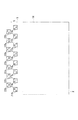
図1に示すように、基台10上には一対のガイドレールを跨ぐようにゲート状構造体16が設けられ、このゲート状構造体16の上面には複数の露光ユニットが描画テーブル14の移動方向に対して直角方向に二列に配列される。第1列目には8つの露光ユニットが含まれ、これら露光ユニットは参照符号181、182、183、184、185、186、187及び188で示される。また、第2列目には7つの露光ユニットが含まれ、これら露光ユニットは201、202、203、204、205、206及び207で示される。第1列目の露光ユニット(181、…188)と第2列目の露光ユニット(201、…207)とは所謂千鳥状に配置される。即ち、第1列目及び第2列目の露光ユニット(181、…188;201、…207)の配列ピッチは共に等しく露光ユニットのほぼ2つ分の幅とされるが、第2列目の露光ユニット(201、…207)の配列ピッチは第1列目の露光ユニット(181、…188)の配列ピッチに対して半ピッチだけずらされている。
【0018】
本実施形態では、各露光ユニット(181、…188;201、…207)はDMDユニットとして構成され、このDMDユニットの反射面は例えば1024×1280のマトリックス状に配列されたマイクロミラーから形成される。各DMDユニットの設置については、描画テーブル14の移動方向に沿って1024個のマイクロミラーが配列されるように行われる。換言すれば、描画テーブル14の移動方向に対して直角方向に1280個のマイクロミラーが配列されることになる。
【0019】
図1に示すように、ゲート状構造体16の上面の適当な箇所には光源22が設けられ、この光源22には複数のLED(light emitting diode)が設けられ、これらLEDから得られる光は集光されて平行光束として光源22の射出口から射出されるようになっている。光源22の射出口には15本の光ファイバケーブル束が接続され、個々の光ファイバケーブルは15個のDMDユニット(181、…188;201、…207)のそれぞれに対して延設され、これにより光源22から各DEDユニットに対して光が導入されるようになっている。なお、図1では、図示の複雑化を避けるために光ファイバケーブルは図示されていない。
【0020】
図2を参照すると、DMDユニット(181、…188;201、…207)の機能が概念図として図示されている。同図において、参照符号24は各DMDユニットの反射面を示し、この反射面24は既に述べたように1024×1280のマトリックス状に配列されたマイクロミラーから形成される。また、図2に示すように、各DMDユニットには、参照符号26で全体的に示す照明光学系と、参照符号28で全体的に示す結像光学系とが組み込まれる。
【0021】
照明光学系26は凸レンズ26A及びコリメートレンズ26Bを含み、凸レンズ26Aは光源22から延設された光ファイバケーブル30と光学的に結合される。このような照明光学系26により、光ファイバケーブル30から射出した光束はDMDユニット(181、…188;201、…207)の反射面24の全体を照明するような平行光束LBに成形される。結像光学系28には第1の凸レンズ28Aと、リフレクタ28Bと、第2の凸レンズ28Cが含まれ、この結像光学系28の倍率は例えば等倍(倍率1)とされる。
【0022】
各DMDユニット(181、…188;201、…207)に含まれる個々のマイクロミラーはそこに入射した光束を結像光学系28に向けて反射させる第1の反射位置と該光束を結像光学系28から逸らすように反射させる第2の反射位置との間で回動変位するように動作させられる。図2では、任意のマイクロミラーが第1の反射位置に置かれたとき、そこから反射されて結像光学系28に入射された光束の光軸が参照符号LB1で示され、同マイクロミラーが第2の反射位置に置かれたとき、そこから反射されて結像光学系28から逸らされた光束の光軸が参照符号LB2で示されている。
【0023】
図2において、描画テーブル14上に設置された被描画体の描画面が参照符号32で示され、この描画面32上には、結像光学系28に入射された光束(LB1)によってマイクロミラーの反射面が結像される。例えば、各DMDユニット(181、…188;201、…207)に含まれる個々のマイクロミラーのサイズが20μm×20μmであるとすると、結像光学系28の倍率は等倍であるから、マイクロミラーの反射面は描画面32上の20μm×20μmの露光領域として結像され、この露光領域が被描画体上に回路パターンを描画する際の一画素となる。要するに、本実施形態では、回路パターンの描画は20μm×20μmの画素サイズで行われる。
【0024】
各描画ユニット(181、…188;201、…207)では、個々のマイクロミラーは通常は第2の反射位置即ち非露光位置に置かれているが、露光作動を行うとき、マイクロミラーは第2の反射位置(非露光位置)から第1の反射位置即ち露光位置に回動変位させられる。マイクロミラーの非露光位置から露光位置への回動変位の制御については、後述するように回路パターンデータ(ラスタデータ)に従って行われる。なお、図2においては、図示の都合上、結像光学系28から逸らされた光束(LB2)も描画面32に向けられているが、しかし実際にはそのような光束(LB2)については描画面32に到達しないように処理されることは言うまでもない。
【0025】
各DMDユニット(181、…188;201、…207)に含まれる全てのマイクロミラーが第1の反射位置即ち露光位置に置かれたときは、全てのマイクロミラーから反射された全光束(LB1)が結像光学系28に入射させられ、このため描画面32上にはDMDユニットの反射面による全露光領域が得られ、その全露光領域のサイズについては(1024×20)μm×(1280×20)μmとなり、そこに含まれる総画素数は勿論1024×1280個となる。
【0026】
ここで以下の説明の便宜上、図3に示すように、被描画体の描画面32を含む平面上にX−Y直交座標系を定義する。なお、同図において、参照符号Z181ないしZ188で示される斜線領域は第1列目の8つの露光ユニット(181、…188)のそれぞれによってX−Y平面上で得られる全露光領域であり、参照符号Z201ないしZ207で示される斜線領域は第2列目の7つの露光ユニット(201、…207)のそれぞれによってX−Y平面上で得られる全露光領域であり、またX−Y直交座標系に対する描画テーブル14の相対位置を明らかにするために該描画テーブル14は想像線(二点鎖線)で図示されている。図3から明らかなように、X−Y直交座標系のX軸は描画テーブル14の移動方向に平行であり、そのY軸は露光ユニット(181、…188;201、…207)の配列方向に平行とされ、しかも第1列目の露光ユニット(181、…188)による全露光領域(Z181、…Z188)の境界に接している。
【0027】
描画装置による描画作動時、描画テーブル14はX軸の負側に一定速度で移動させられ、これにより描画テーブル14上の被描画体は露光ユニット(181、…188;201、…207)の個々のマイクロミラーからの反射光束でもって走査され得る。従って、描画テーブル14の移動中、先ず、第1列目のDMDユニット(181、…188)を露光作動させて8つの全面露光領域(Z181、…Z188)を描画面32上に形成した後に所定のタイミングだけ遅れて第2列目の露光ユニット(201、…207)を露光動作させて7つの全面露光領域(Z201、…Z207)を描画面32上に形成することにより、8つの全面露光領域(Z181、…Z188)と7つの全面露光領域(Z201、…Z207)とを描画面32上でY軸方向に沿って整列させることが可能であり、このときY軸方向に沿うそれぞれの一ラインに含まれる総画素数は1280×15個となる。
【0028】
本発明による描画装置にあっては、描画テーブル14を所定の一定速度で連続的に移動させつつ、回路パターンデータ(ラスタデータ)に従って回路パターンを多重露光により描画する描画法が採られ、このような描画法の原理について以下に説明する。
【0029】
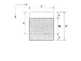
先ず、図4及び図5を参照して、本発明による描画法での一画素の定義について説明する。図4には、DMDユニット(181、…188;201、…207)の任意のマイクロミラーが第2の反射位置即ち非露光位置から第1の反射位置即ち露光位置に回動変位させられた際に、該マイクロミラーの反射面から反射された光束によって被描画体上に投影(結像)された一画素露光領域が斜線領域として示され、この一画素露光領域のサイズはC×Cとされる。なお、本実施形態では、上述したように、C=20μmである。本発明による描画法にあっては、描画テーブル14は一定速度で連続的に移動させられ、描画テーブル14がX軸の負側に向かってC(20μm)以下の距離dだけ移動した後、上述のマイクロミラーは露光位置(第1の反射位置)から非露光位置(第2の反射位置)に戻される。要するに、マイクロミラーが露光位置に留められる時間が露光時間となり、この露光時間は描画テーブル14がX軸の負側に向かって距離d(d<C)だけ移動する時間に一致する。
【0030】
換言すれば、そのような露光時間中に、一画素露光領域は図5に示すようにその初期露光位置(破線で示す)から距離dだけX軸の正側に描画面32上を移動することになり、このとき一画素露光領域のX軸方向に沿う全露光区間TEの露光量の分布は図6のグラフに示すようなものとなる。即ち、一画素露光領域がX軸の正側に向かって移動するものとすると、その後続縁の移動距離区間(d)にわたって露光量は零から最大露光量pに向かって次第に増大し、次いで最大露光量区間MEにわたって最大露光量pが維持され、続いて該一画素露光領域の先導縁の移動距離区間(d)にわたって露光量は最大露光量pから零に向かって次第に減少する。
【0031】
このような露光量分布について露光量p/2以上の露光量区間C′とすると、この露光量区間C′は一画素露光領域のX軸方向に沿うサイズCに一致する。かくして、図7に示すように、露光量p/2以上の露光量領域(斜線領域)は当初の一画素露光領域に等しいサイズ(C′×C)を持つこととなり、本発明による描画法では、そのような露光量領域が一画素露光領域として定義される。なお、露光量p/2の具体的な数値については被描画体(フォトレジスト層等)の感度に基づいて設定されるものであって、そのような設定数値の露光量が得られるように光源装置の光強度、露光時間(距離d)等のパラメータが決定される。
【0032】
次に、以上のように定義される一画素露光領域によって回路パターンを実際に描画する際の描画法について具体的に説明する。
【0033】
先ず、図8を参照すると、ビット・マップ・メモリ上に展開された回路パターンデータ(ラスタデータ)の一部が模式的に示されている。同図に示すライン番号Nは描画面32上にY軸に沿って順次描画されるべき描画ラインの番号に対応し、各ラインは1280×15個のビットデータから構成される。図8に示すように、各ラインに含まれる1280×15個のビットデータは1280ビット毎に第1番目ないし第15番目のグループに分けられ、第1列目の8つのDMDユニット(181、…188)の露光作動はそれぞれ奇数番目のグループのビットデータに従って行われ、第2列目の7つのDMDユニット(201、…207)の露光作動はそれぞれ偶数番目のグループのビットデータに従って行われる。
【0034】
図8に示すように、本発明による描画法に従ってDMD181を露光作動させる際の以下の例示的な説明のために、第1番目のグループのライン番号1ないし9のそれぞれの上位4ビットには“1”が与えられ、残りの1276ビットには“0”が与えられる。なお、図8では、その他のビットデータについてはすべてDで示され、このDには“1”か“0”のうちのいずれかの値が与えられる。
【0035】
図9を参照すると、第1番目のグループのビットデータに従ってDMDユニット181によって描画を行う際の手順が模式的に示されている。なお、描画作動中、描画テーブル14が実際にはX軸に沿ってその負側に向かって移動させられることになるが、ここでは、説明の便宜上、DMDユニット181がX軸に沿ってその正側に向かって移動するものとされる。
【0036】
DMDユニット181が被描画体の描画面32上の描画開始位置に到達したとき(即ち、描画面32上の描画開始位置がY軸に到達したとき)、DMDユニット181のY軸に沿う第1ライン目の1280個のマイクロミラーのそれぞれが第1番目のグループのライン番号1に含まれる1280個のビットデータ[11110…00000]に従って動作させられ、これによりDMDユニット181の第1回目露光作動が行われる。即ち、第1番目のグループのライン番号1の1280個のビットデータ[11110…00000]のうちの上位4ビットデータ“1”にそれぞれ対応した4つのマイクロミラーだけが非露光位置(第2の露光位置)から露光位置(第1の反射位置)に回動変位させられる。各マイクロミラーが露光位置に留められる時間即ち露光時間については、図4ないし図7を参照して説明したように、DMDユニット181がX軸の正側に向かって距離d(d<C)だけ移動する時間とされる。かくして、図9に示すように、第1回目露光作動時に、被描画体の描画面32上には上述の4つのマイクロミラーにより4画素分の一画素露光領域(斜線領域)が得られる。第1回目露光作動によって4画素分の一画素露光領域(斜線領域)が形成された後、DMDユニット181が描画開始位置からX軸の正側に向かって画素サイズ(C)の整数倍の距離例えば画素サイズの4倍の距離Aだけ移動させられると、第2回目露光作動が開始される。
【0037】
第2回目露光作動時、図9に示すように、DMDユニット181のY軸に沿う第1ラインの1280個のマイクロミラーのそれぞれは第1番目のグループのライン番号5の1280個のビットデータ[11110…00000]に従って動作させられ、DMDユニット181のY軸に沿う第2ラインの1280個のマイクロミラーのそれぞれは第1番目のグループのライン番号4の1280個のビットデータ[11110…00000]に従って動作させられ、DMDユニット181のY軸に沿う第3ラインの1280個のマイクロミラーのそれぞれは第1番目のグループのライン番号3の1280個のビットデータ[11110…00000]に従って動作させられる。同様に、DMDユニット181のY軸に沿う第4ラインの1280個のマイクロミラーのそれぞれは第1番目のグループのライン番号2の1280個のビットデータ[11110…00000]に従って動作させられ、DMDユニット181のY軸に沿う第5ラインの1280個のマイクロミラーのそれぞれは第1番目のグループのライン番号1の1280個のビットデータ[11110…00000]に従って動作させられる。
【0038】
勿論、第2回目露光作動時の露光時間も第1回目露光作動時の露光時間と同じとされ、このとき第1番目のグループのライン番号1ないし5の各ライン番号に含まれる上位4ビットデータ“1”にそれぞれ対応した4つのマイクロミラーにより被描画体の描画面32上には4画素分の一画素露光領域(斜線領域)が得られる。ここで注目すべきことは、第1回目露光作動時に得られた4画素分の一画素露光領域(斜線領域)が第2回目露光作動時に第1番目のグループのライン番号1の上位4ビットデータ “1”に従って二重露光されるということである。第2回目露光作動の開始後、DMDユニット181がX軸の正側に向かって再び距離A(=4C)だけ移動させられると、第3回目露光作動が開始される。
【0039】
第3回目露光作動時、図9に示すように、DMDユニット181のY軸に沿う第1ラインの1280個のマイクロミラーのそれぞれは第1番目のグループのライン番号9の1280個のビットデータ[11110…00000]に従って動作させられ、DMDユニット181のY軸に沿う第2ラインの1280個のマイクロミラーのそれぞれは第1番目のグループのライン番号8の1280個のビットデータ[11110…00000]に従って動作させられ、DMDユニット181のY軸に沿う第3ラインの1280個のマイクロミラーのそれぞれは第1番目のグループのライン番号7の1280個のビットデータ[11110…00000]に従って動作せられる。同様に、DMDユニット181のY軸に沿う第4ラインの1280個のマイクロミラーのそれぞれは第1番目のグループのライン番号6の1280個のビットデータ[11110…00000]に従って動作させられ、DMDユニット181のY軸に沿う第5ラインの1280個のマイクロミラーのそれぞれは第1番目のグループのライン番号5の1280個のビットデータ[11110…00000]に従って動作させられ、DMDユニット181のY軸に沿う第6ラインの1280個のマイクロミラーのそれぞれは第1番目のグループのライン番号4の1280個のビットデータ[11110…00000]に従って動作させられる。更に、DMDユニット181のY軸に沿う第7ラインの1280個のマイクロミラーのそれぞれは第1番目のグループのライン番号3の1280個のビットデータ[11110…00000]に従って動作させられ、DMDユニット181のY軸に沿う第8ラインの1280個のマイクロミラーのそれぞれは第1番目のグループのライン番号2の1280個のビットデータ[11110…00000]に従って動作させられ、DMDユニット181のY軸に沿う第9ラインの1280個のマイクロミラーのそれぞれは第1番目のグループのライン番号1の1280個のビットデータ[11110…00000]に従って動作させられる。
【0040】
第3回目露光作動時の露光時間も第1回目露光作動時の露光時間と同じであり、このとき第1番目のグループのライン番号1ないし9の各ライン番号に含まれる上位4ビットデータ“1”にそれぞれ対応した4つのマイクロミラーにより被描画体の描画面32上には4画素分の一画素露光領域(斜線領域)が得られることになる。上述の場合と同様に、第1回目露光作動時に得られた4画素分の一画素露光領域(斜線領域)は第2回目露光作動時と第3回目露光作動時とで第1番目のグループのライン番号1の上位4ビットデータ “1”に従って三重露光され、また第2回目露光作動時にライン番号2ないし5のそれぞれの上位4ビットデータ“1”によって得られた4画素分の一画素露光領域(斜線領域)は第3回目露光作動時にライン番号2ないし5のそれぞれの上位4ビットデータ“1”によって二重露光される。
【0041】
以上述べようたように、DMDユニット181が描画開始位置からX軸の正側に向かって距離A(=4C)だけ移動させられる度毎に露光作動が繰り返される。DMDユニット181のY軸に沿うラインの本数は1024本であるから、上述の例では、露光作動の繰返し数は1024/4=256となる。従って、例えば、第1番目のグループのライン番号1に含まれる上位4ビットデータ“1”によって得られる4画素分の一画素露光領域の各々は256回にわたって多重露光されることになる。図10を参照すると、上述の一画素露光領域のうちの1つが6回の多重露光作動によって得られた際の多重露光量がグラフ化して図示され、その多重露光量の総計は勿論6pとなる。もし256回の多重露光作動が行われれば、その多重露光量の総計は256pとなる。
【0042】
第1列目に含まれるその他のDMDユニット182ないし188の露光作動のそれぞれについても、上述の場合と同様な態様で、第3番目、第5番目、第7番目、第9番目、第11番目、第13番目及び第15番目のグループのビットデータに従って行われ、そのいずれかのビットデータDに“1”が与えられるているとき、そのビットデータに対応した一画素露光領域についても256回にわたって多重露光が行われる。また、第2列目に含まれるDMDユニット201ないし207の露光作動のそれぞれについても、上述の場合と同様な態様で、第2番目、第4番目、第6番目、第8番目、第10番目、第12番目及び第14番目のグループのビットデータに従って行われるが、しかし第2列目のDMDユニット201ないし207の作動タイミングについては第1列目のDMDユニット181ないし188に対する2列目のDMDユニット201ないし207のX軸方向のシフト距離sだけ遅らされる(図3)。即ち、第2列目のDMDユニット201ないし207が被描画体の描画面32上に描画開始位置に到達したとき、第2列目のDMDユニット201ないし207による露光作動が開始される。
【0043】
上述の例では、距離Aを画素サイズ(C)の4倍とすることで多重露光回数については256回とされているが、このような露光回数(即ち、距離A)は被描画体(本実施形態では、フォトレジスト層)の感度、光源22の光強度及び描画テーブル14の速度等に基づいて決められ、これにより各一画素露光領域について所望の露光量が得られるようにされる。
【0044】
図11を参照すると、本発明による描画装置の制御ブロック図が示される。同図に示すように、本発明による描画装置にはシステムコントロール回路34が設けられ、このシステムコントロール回路34は例えばマイクロコンピュータから構成される。即ち、システムコントロール回路34は中央演算処理ユニット(CPU)、種々のルーチンを実行するためのプログラム、定数等を格納する読出し専用メモリ(ROM)、データ等を一時的に格納する書込み/読出し自在なメモリ(RAM)及び入出力インターフェース(I/O)から成り、描画装置の作動全般を制御する。
【0045】
システムコントロール回路34はLAN(local area network)を介してCADステーション或いはCAMステーションに接続され、CADステーション或いはCAMステーションからはそこで作成処理された回路パターンデータ(ベクタデータ)がシステムコントロール回路34に転送される。システムコントロール回路34にはデータ格納手段としてハードディスク装置36が接続され、CADステーション或いはCAMステーションから回路パターンデータ(ベクタデータ)がシステムコントロール回路34に転送されると、システムコントロール回路34は回路パターンデータ(ベクタデータ)を一旦ハードディスク装置36に書き込んで格納する。また、システムコントロール回路34には外部入力装置としてキーボード38が接続され、このキーボード38を介して種々の指令信号や種々のデータ等がシステムコントロール回路34に入力される。
【0046】
図11において、参照符号40はラスタ変換回路を示し、参照符号42はビット・マップ・メモリを示す。描画作動に先立って、ハードディスク装置36から回路パターンデータ(ベクタデータ)が読み出されてラスタ変換回路40に出力され、この回路パターンデータ(ベクタデータ)はラスタ変換回路40によってラスタデータに変換される。このように変換された回路パターンデータ(ラスタデータ)はビット・マップ・メモリ42に書き込まれる。ラスタ変換回路40でのデータ変換処理及びビット・マップ・メモリ42でのデータ書込みについてはキーボード38を介して入力される指令信号により行われる。
【0047】
勿論、ビット・マップ・メモリ42に展開された回路パターンデータ(ラスタデータ)は図8に模式的に示すようなものとなる。即ち、図8を参照して説明したように、各ライン番号Nによって示される一ラインには、1280×15個のビットデータが含まれ、これら1280×15個のビットデータは1280ビット毎に第1番目ないし第15番目のグループに分けられる。先に説明したように、第1列目の8つのDMDユニット(181、…188)の露光作動はそれぞれ奇数番目のグループのビットデータに従って行われ、また第2列目の7つのDMDユニット(201、…207)の露光作動はそれぞれ偶数番目のグループのビットデータに従って露光作動が行われる。
【0048】
図11において、参照符号44はDMD駆動回路を示し、このDMD駆動回路44により、第1列目の8つのDMDユニット(181、…188)と第2列目の7つのDMDユニット(201、…207)との露光作動が制御される。このような露光動作は勿論ビット・マップ・メモリ42から各ライン番号毎に読み出されるビットデータに従って行われ、このときビットデータの読み出されるライン番号は描画テーブル14の移動量に応じて規則的に変化させられる。なお、図11では、第1列目の8つのDMDユニット(181、…188)と第2列目の7つのDMDユニット(201、…207)との露光作動が破線矢印で模式的に図示されている。
【0049】
第1列目の8つのDMDユニット(181、…188)の露光作動をDMD駆動回路44によって制御する際にビット・マップ・メモリ42の奇数番目の各グループからビットデータを読み出すべきライン番号について説明すると、DMDユニット(181、…188)が被描画体の描画面32上の描画開始位置に到達したとき、第1回目露光作動が開始され、このときビット・マップ・メモリ42の奇数番目の各グループからライン番号1のビットデータが読み出され(図9)、このライン番号1のビットデータに従って第1列目の8つのDMDユニット(181、…188)のY軸に沿う第1ラインの1280個のマイクロミラーが動作させられる。
【0050】
DMDユニット(181、…188)が描画開始位置からX軸の正側に距離Aだけ移動したとき、第2回目露光作動が開始され、このときビット・マップ・メモリ42の奇数番目の各グループからはライン番号1からライン番号(A/C+1)までのビットデータが読み出される。上述した例では、A=4Cであるので、第2回目露光作動時にはビット・マップ・メモリ42の奇数番目の各グループからはライン番号1からライン番号5(=4C/C+1)までのビットデータが読み出され(図9)、これらビットデータに従って第1列目の8つのDMDユニット(181、…188)のY軸に沿う第5ラインないし第1ラインの各ラインの1280個のマイクロミラーが動作させられる。
【0051】
上述したように、DMDユニット(181、…188)の露光作動は描画開始位置からX軸の正側に距離Aずつ移動する度毎に繰り返されるので、DMDユニット(181、…188)が描画開始位置からX軸の正側に距離Sだけ移動した際の露光回数iは以下の式で表せる。
i=INT[S/A]+1
ここで、演算子INT[S/A]は除算S/Aの商を表し、S<Aであるとき、INT[S/A]=0として定義される。
【0052】
従って、第i回目露光作動時、ビット・マップ・メモリ42の奇数番目の各グループから読み出されるべきビットデータの最終ライン番号Nは以下の式で表せる。
N=((i-1)*A/C+1)
【0053】
また、本実施形態においては、各DMDユニット(181、…188)のY軸に沿う総ライン数は1024であるから、最終ライン番号((i-1)*A/C+1)が1024を越えたとき、ビット・マップ・メモリ42の奇数番目の各グループから読み出されるべきビットデータの最大ライン数は1024本となる。例えば、上述の例(A=4C)において、露光回数が257回目になったとき、ビット・マップ・メモリ42の奇数番目の各グループから読み出されるべきビットデータの最終ライン番号N(=256*4C/C+1)は1025となり、この場合にはライン番号2からライン番号1025までの1024本のラインのビットデータが読み出されることになる。
【0054】
一般的に言うと、以下の演算結果に基づいて、ビット・マップ・メモリ42の奇数番目の各グループから読み出されるべきビットデータのライン数を確定することができる。
((i-1)*A/C+1)−1024=I
【0055】
即ち、I≦0のときは、ライン番号1からライン番号((i-1)*A/C+1)までのビットデータがビット・マップ・メモリ42の奇数番目の各グループから読み出される。また、I>0であるときには、ライン番号(I+1)からライン番号((i-1)*A/C+1)までのビットデータがビット・マップ・メモリ42の奇数番目の各グループから読み出される。なお、ライン番号(I+1)からライン番号((i-1)*A/C+1)までのラインの総本数は1024本となる。
【0056】
なお、第2列目の7つのDMDユニット(201、…207)の露光作動をDMD駆動回路44によって制御する際にビット・マップ・メモリ42の偶数番目の各グループからビットデータを読み出すべきライン番号の説明についても上述した場合と同様なことが言える。即ち、第2列目の7つのDMDユニット(201、…207)による露光作動時、ビット・マップ・メモリ42の偶数番目の各グループのそれぞれの該当ラインからビットデータを読み出す際のタイミングが第1列目のDMDユニット181ないし188に対する第2列目のDMDユニット201ないし207のX軸方向のシフト距離sだけ遅らされるだけである(図3)。
【0057】
図11において、参照符号46は描画テーブル14をX軸方向に沿って駆動させるための駆動モータを示す。勿論、描画テーブル14と駆動モータ46との間には先に述べたようにボール螺子等を含む駆動機構が介在させられるが、そのような駆動機構については図11では破線矢印で象徴的に示されている。駆動モータ46は例えばステッピングモータとして構成され、その駆動制御は駆動回路48から出力される駆動パルスに従って行われる。
【0058】
駆動回路48はX軸制御回路50の制御下で動作させられ、このX軸制御回路50は描画テーブル14に設けられたX位置検出センサ52に接続される。X位置検出センサ52は描画テーブル14の移動経路に沿って設置されたX軸リニアスケール54からの光信号を検出して描画テーブル14のX軸方向に沿うその位置を検出するものである。なお、図11では、X軸リニアスケール54からの光信号の検出が破線矢印で象徴的に示されている。
【0059】
描画テーブル14の移動中、X位置検出センサ52はX軸リニアスケール54から一連の光信号を順次検出して一連の検出信号(パルス)としてX軸制御回路50に対して出力する。X軸制御回路50では、そこに入力された一連の検出信号が適宜処理され、その検出信号に基づいて一連の制御クロックパルスが作成される。X軸制御回路50からは一連の制御クロックパルスが駆動回路48に対して出力され、駆動回路48ではその一連の制御クロックパルスに従って駆動モータ46に対する駆動パルスが作成される。要するに、X軸リニアスケール54の精度に応じた正確さで描画テーブル14をX軸方向に沿って移動させることができる。なお、このような描画テーブル14の移動制御自体は周知のものである。
【0060】
図11に示すように、X軸制御回路50はシステムコントロール回路34に接続され、これによりX軸制御回路50はシステムコントロール回路34の制御下で行われる。一方、X位置検出センサ52から出力される一連の検出信号(パルス)はX軸制御回路50を介してシステムコントロール回路34にも入力され、これによりシステムコントロール回路34では描画テーブル14のX軸に沿う移動位置を常に監視することができる。
【0061】
図12ないし図14を参照すると、システムコントロール回路34で実行される描画ルーチンのフローチャートが示され、この描画ルーチンの実行は描画装置の電源スイッチ(図示されない)をオンすることにより開始される。
【0062】
ステップ1201では、キーボード38上に割り当てられた描画開始キーが操作されたか否かが判断される。なお、描画開始キーの操作前には、回路パターンデータ(ベクタデータ)からラスタデータへの変換処理が行われていてビット・マップ・メモリ42には回路パターンデータ(ラスタデータ)が既に展開されているものとされ、また描画ルーチンの実行に必要な種々のデータ、例えば距離A、描画時間、描画テーブル14の移動速度等のデータはキーボード38を介して入力されてシステムコントロール回路34のRAMに既に格納されているものとする。
【0063】
ステップ1201で描画開始キーの操作が確認されると、ステップ1202に進み、そこでフラグF1及びF2は“0”に初期化され、またカウンタi及びjは“1”に初期化される。
【0064】
フラグF1は第1列目のDMDユニット(181、…188)の描画作動が完了したか否かを指示するためのフラグである。第1列目のDMDユニット(181、…188)による描画作動が完了すると、フラグF1は“0”から“1”に書き換えられる。
【0065】
フラグF2は第2列目のDMDユニット(201、…207)が画体の描画面32上の描画開始位置に到達したか否かを指示するためのフラグである。第2列目のDMDユニット(201、…207)が描画開始位置に到達したとが確認されると、フラグF2は“0”から“1”に書き換えられる。
【0066】
カウンタiは第1列目のDMDユニット(181、…188)によって行われる露光作動の回数をカウントするものであり、またカウンタjは第2列目のDMDユニット(201、…207)によって行われる露光作動の回数をカウントするもである。従って、カウンタi及びjのそれぞれには初期値として“1”が設定される。
【0067】
ステップ1203では、駆動モータ46が始動されて描画テーブル14がその原点位置からX軸の負側に向かって所定の一定速度で移動させられる。換言すれば、第1列目のDMDユニット(181、…188)及び第2列目のDMDユニット(201、…207)が描画テーブル14に対してX軸の正側に移動することとなる。なお、ここでは、描画テーブル14上には被描画体が所定位置に設置されていて、その被描画体の描画面上の描画開始位置は描画テーブル14の原点位置でX−Y座標系に対して特定されているものとされる。
【0068】
ステップ1204では、第1列目のDMDユニット(181、…188)が描画開始位置に到達したか否かが監視される。描画開始位置への第1列目のDMDユニット(181、…188)の到達が確認されると、ステップ1205に進み、そこでフラグF1が“0”であるか“1”であるかが判断される。初期段階では、F1=0であるので、ステップ1206に進み、そこで以下の演算が行われる。
I←((i-1)*A/C+1)−1024
【0069】
ステップ1207では、Iが“0”以下であるか否かが判断される。上記演算式の意味は既に述べた通りであり、第1列目のDMDユニット(181、…188)による第1回目露光作動時には、I<0であるので、ステップ1208に進み、そこでビット・マップ・メモリ42の奇数番目の各グループのライン番号1からライン番号((i-1)*A/C+1)までのビットデータが読み出されるが、しかしi=1のとき、((i-1)*A/C+1)=1となるので、この場合には該奇数番目の各グループのライン番号1からビットデータが読み出される。
【0070】
ステップ1210では、第1列目のDMDユニット(181、…188)による露光作動が開始され、この露光作動は第1回目露光作動となる(i=1)。要するに、ビット・マップ・メモリ42の奇数番目の各グループのライン番号1から読み出されたビットデータに従って第1列目のDMDユニット(181、…188)のY軸に沿う第1ラインの1280個のマイクロミラーが動作させられ、これにより第1回目露光作動が開始される。第1回目露光作動の開始後、ステップ1211に進み、そこでカウンタiのカウント数が“1”だけインクレメントされ、第1列目のDMDユニット(181、…188)による第2回目露光作動に備える。
【0071】
ステップ1212では、フラグF2が“0”であるか“1”であるかが判断される。初期段階では、F2=0であるので、ステップ1213に進み、そこで第2列目のDMDユニット(201、…207)が描画開始位置に到達したか否かが判断される。この初期段階では、第2列目のDMDユニット(201、…207)は描画開始位置に到達していなので、ステップ1221にスキップし、第1列目のDMDユニット(181、…188)による描画作動が完了したか否かが判断される。
【0072】
この初期段階では、第1列目のDMDユニット(181、…188)による描画作動は完了していないので、ステップ1221からステップ1222に進み、そこで第1列目のDMDユニット(181、…188)が露光作動開始時から距離dだけ移動したか否かが監視される。勿論、先に述べたように、距離dは一画素露光領域のサイズC(20μm)以下の距離となる。ステップ1222で第1列目のDMDユニット(181、…188)による距離dの移動が確認されると、ステップ1223に進み、そこで第1列目のDMDユニット(181、…188)による露光作動が停止される。
【0073】
ステップ1224では、第1列目のDMDユニット(181、…188)が描画開始位置から距離Aの倍数だけ移動したか否かが監視される。第1列目のDMDユニット(181、…188)の描画開始位置から距離Aの倍数までの移動が確認されると、ステップ1205に戻る。即ち、第1列目のDMDユニット(181、…188)による露光作動が繰り返されて(ステップ1210)、カウンタiのカウント数が“1”ずつインクレメントとされる(ステップ1211)。
【0074】
先に述べたように、A=4Cの例では、一画素露光領域については256回にわたって多重露光が行われる。このような例においては、カウンタiのカウント数が256に到達するまでは、I<0であるので、256回目までの露光作動では、ビット・マップ・メモリ42の奇数番目の各グループのライン番号1からライン番号((i-1)*A/C+1)までのビットデータが読み出されることになる(ステップ1208)。しかしながら、カウンタiのカウント数が257以上になると、I>0となり、このときステップ1207からステップ1209に進み、そこでビット・マップ・メモリ42の奇数番目の各グループからビットデータが読み出されるべきライン番号は(I+1)から((i-1)*A/C+1)までとなる。勿論、この場合には、ビット・マップ・メモリ42の奇数番目の各グループからビットデータが読み出されるラインの総数は1024本となる。
【0075】
第1列目のDMDユニット(181、…188)による露光作動中に、ステップ1213で描画開始位置への第2列目のDMDユニット(201、…207)の到達が確認されると、ステップ1213からステップ1214に進み、そこでフラグF2が“0”から“1”に書き換えられる。次いで、ステップ1215に進み、そこで以下の演算が行われる。
J←((j-1)*A/C+1)−1024
【0076】
ステップ1216では、Jが“0”以下であるか否かが判断される。上記演算式の意味は既に述べた通りであり、第2列目のDMDユニット(201、…207)による第1回目露光作動時には、J<0であるので、ステップ1217に進み、そこでビット・マップ・メモリ42の偶数番目の各グループのライン番号1からライン番号((j-1)*A/C+1)までのビットデータが読み出されるが、しかしj=1のとき、((j-1)*A/C+1)=1となるので、この場合には該偶数番目の各グループのライン番号1からビットデータが読み出される。
【0077】
ステップ1219では、第2列目のDMDユニット(201、…207)による露光作動が開始され、この露光作動は第1回目露光作動となる(j=1)。要するに、ビット・マップ・メモリ42の偶数番目の各グループのライン番号1から読み出されたビットデータに従って第2列目のDMDユニット(201、…207)のY軸に沿う第1ラインの1280個のマイクロミラーが動作させられ、これにより第1回目露光作動が開始される。第1回目露光作動の開始後、ステップ1220に進み、そこでカウンタjのカウント数が“1”だけインクレメントされ、第2列目のDMDユニット(201、…207)による第2回目露光作動に備える。
【0078】
ステップ1220でカウンタjのカウント数が“1”だけインクレメントされた後に、ステップ1221に進み、そこで第1列目のDMDユニット(181、…188)による描画作動が完了したか否かが判断される。第1列目のDMDユニット(181、…188)による描画作動が完了していないとき、ステップ1222に進み、そこで第1列目のDMDユニット(181、…188)と第2列目のDMDユニット(201、…207)とが露光作動開始時から距離dだけ移動したか否かが監視される。ステップ1222で第1列目のDMDユニット(181、…188)と第2列目のDMDユニット(201、…207)とによる距離dの移動が確認されると、ステップ1223に進み、そこで第1列目のDMDユニット(181、…188)と第2列目のDMDユニット(201、…207)とによる露光作動が停止される。
【0079】
ステップ1224では、第1列目のDMDユニット(181、…188)と第2列目のDMDユニット(201、…207)とが描画開始位置から距離Aの倍数だけ移動したか否かが監視される。ステップ1224で第1列目のDMDユニット(181、…188)と第2列目のDMDユニット(201、…207)との描画開始位置から距離Aの倍数までの移動が確認されると、ステップ1205に戻る。即ち、第1列目のDMDユニット(181、…188)による露光作動と第2列目の第2列目のDMDユニット(201、…207)による露光作動とが繰り返されて(ステップ1210及びステップ1219)、カウンタi及びjのカウント数が“1”ずつインクレメントされる(ステップ1211及びステップ1220)。なお、この時点では、F2=1となっているために、ステップ1212からステップ1213及び1214を迂回してステップ1215に進むことになる。
【0080】
第1列目のDMDユニット(181、…188)による露光作動の場合と同様に、第2列目のDMDユニット(201、…207)による露光作動の場合においても、A=4Cの例では、一画素露光領域については256回にわたって多重露光が行われる。従って、カウンタjのカウント数が256に到達するまでは、J<0であるので、256回目までの露光作動では、ビット・マップ・メモリ42の偶数番目の各グループのライン番号1からライン番号((j-1)*A/C+1)までのビットデータが読み出されることになる(ステップ1217)。しかしながら、カウンタjのカウント数が257以上になると、J>0となり、このときステップ1216からステップ1218に進み、そこでビット・マップ・メモリ42の偶数番目の各グループからビットデータが読み出されるべきライン番号は(J+1)から((j-1)*A/C+1)までとなる。勿論、この場合には、ビット・マップ・メモリ42の偶数番目の各グループからビットデータが読み出されるラインの総数は1024本となる。
【0081】
ステップ1221で第1列目のDMDユニット(181、…188)による描画作動が完了したことが確認されると、ステップ1221からステップ1225に進み、そこでフラグF1が“0”から“1”に書き換えられる。次いで、ステップ1226では、第2列目のDMDユニット(201、…207)による描画作動が完了したか否かが判断される。第2列目のDMDユニット(201、…207)による描画作動が完了していないとき、ステップ1226からステップ1222に進み、そこで第2列目のDMDユニット(201、…207)が露光作動開始時から距離dだけ移動したか否かが監視される。第2列目のDMDユニット(201、…207)による距離dの移動が確認されると、ステップ1223に進み、そこで第2列目のDMDユニット(201、…207)による露光作動が停止される。
【0082】
ステップ1224では、第2列目のDMDユニット(201、…207)が描画開始位置から距離Aの倍数だけ移動したか否かが監視される。第2列目のDMDユニット(201、…207)の描画開始位置から距離Aの倍数までの移動が確認されると、ステップ1205に戻るけれども、このときF1=1となっているので、ステップ1205からステップ1212までスキップし、このため第2列目のDMDユニット(201、…207)による露光作動だけが繰り返されて(ステップ1219)、カウンタjのカウント数が“1”ずつインクレメントされる(ステップ1220)。
【0083】
ステップ1226で第2列目のDMDユニット(201、…207)による描画作動が完了したことが確認されると、ステップ1226からステップ1227に進み、そこで駆動モータ46が逆駆動させられて描画テーブル14はその原点位置に向かって戻される。次いで、ステップ1228では、描画テーブル14が原点位置に到達したか否かが監視され、描画テーブル14の原点位置への到達が確認されると、駆動モータ46の駆動が停止されて、本ルーチンの実行が終了する。
【0084】
【発明の効果】
以上の記載から明らかなように、本発明にあっては、マトリックス状に配列された多数の変調素子を持つ露光ユニットを用いて行う従来の露光方式、即ちステップ・アンド・リピート方式とは異なって、該露光ユニットを描画テーブルに対して相対的に一定速度で連続的に移動させつつ描画を行うことができるので、回路パターンの全体の描画に必要とされる時間を短縮し得るという作用効果が得られる。なお、双方の全体の描画時間についての具体的な比較はないが、しかしステップ・アンド・リピート方式では、露光時間と描画テーブルの移動時間とは別々のものであるのに対して、本発明による多重露光描画方法では、露光時間が描画テーブルの移動時間中に含まれるということから、本発明による全体の描画時間の短縮化については明らかである。
【0085】
また、本発明にあっては、従来のステップ・アンド・リピート方式のように、描画テーブルが間欠的に繰り返し移動させられることはないので、描画テーブルを頻繁に加速及び減速させる必要はなく、このため描画テーブルの駆動系が故障し難いという作用効果も得られる。
【0086】
本発明により得られる特徴的な作用効果の1つとして、露光ユニット内の変調素子の幾つかが正常に機能しなくなったとしても、画素欠陥を生じさせることなく回路パターンの描画を適正に行い得るという点も挙げられる。というのは、描画回路パターンの個々の一画素露光領域は数百回以上の露光作動にわたる多重露光によって得られるので、そのうちの数回程度の露光作動が正常に行われなかったとしても、その一画素露光領域の総露光量は十分に得られるからである。
【0087】
また、本発明により得られる特徴的な別の作用効果として、個々の露光ユニットに組み込まれる結像光学系に起因する露光むらがあったとしても、その露光むらの影響は数百回以上の多重露光のために小さくされるという点も挙げられる。
【0088】
本発明により得られる特徴的な更に別の作用効果として、光源装置の出力が低くても、数百回以上の多重露光のために十分な露光量が確保し得る点も挙げられる。換言すれば、本発明による多重露光描画方法及び多重露光描画装置に用いれる光源装置については安価に構成し得ることになる。
【図面の簡単な説明】
【図1】本発明による多重露光描画装置の概略斜視図である。
【図2】本発明による多重露光描画装置で用いるDMDユニットの機能を説明するための概略概念図である。
【図3】図1に示す多重露光描画装置の描画テーブル上の被描画体の描画面を含む平面上に定義されたX−Y直交座標系を説明するための平面図である。
【図4】本発明による多重露光描画装置のDMDユニットの個々のマイクロミラーによって得られる一画素露光領域を示す平面図である。
【図5】図4と同様な平面図であって、図4に示す一画素露光領域がそのサイズ以下の距離だけ移動した状態を示す図である。
【図6】図4に示す一画素露光領域が図5に示す位置まで連続的に移動した際の露光量分布を示すグラフである。
【図7】図4及び図5と同様な平面図であって、図6に示す露光量分布に基づいて本発明に従って定義される一画素露光領域を示す図である。
【図8】本発明による多重露光描画装置で描画するべき回路パターンの描画データ(ラスタデータ)の一部をビット・マップ・メモリ上に展開された状態で示す模式図である。
【図9】本発明による多重露光描画装置により図8の描画データに基づいて回路パターンを多重露光方式で描画する際の原理を説明するための図である。
【図10】図9に示した多重露光方式で描画された際の一画素露光領域の多重露光量を示すグラフである。
【図11】本発明による多重露光描画装置のブロック図である。
【図12】本発明による多重露光描画装置で実行される描画ルーチンのフローチャートの一部分である。
【図13】本発明による多重露光描画装置で実行される描画ルーチンのフローチャートのその他の部分である。
【図14】本発明による多重露光描画装置で実行される描画ルーチンのフローチャートの残りの部分である。
【符号の説明】
10 基台
12 ガイドレール
14 描画テーブル
16 ゲート状構造体
181…188 第1列目の露光ユニット
201…207 第2列目の露光ユニット
24 各DMDユニットの反射面
26 各DMDユニットの照明光学系
28 各DMDユニットの結像光学系
30 光ファイバケーブル
32 描画面
34 システムコントロール回路
36 ハードディスク装置
38 キーボード
40 ラスタ変換回路
42 ビット・マップ・メモリ
44 DMD駆動回路
46 駆動モータ
48 駆動回路
50 X軸制御回路
52 X位置検出センサ
54 X軸リニアスケール[0001]
BACKGROUND OF THE INVENTION
The present invention relates to a drawing method and a drawing apparatus for drawing a predetermined pattern on a drawing surface using an exposure unit having a large number of modulation elements arranged in a matrix.
[0002]
[Prior art]
A drawing apparatus as described above is generally used for optically drawing a fine pattern or a symbol such as a character on the surface of an appropriate drawing object. A typical example of use is drawing a circuit pattern when a printed circuit board is manufactured by a photolithography technique. In this case, the object to be drawn is on a photosensitive film for a photomask or on the board. It becomes a photoresist layer.
[0003]
In recent years, a series of processes from a circuit pattern design process to a drawing process are integrated into a system, and the drawing apparatus plays a part in such an integrated system. In the integrated system, in addition to a drawing device, a CAD (Computer Aided Design) station for designing a circuit pattern, and a CAM (Computer Aided) for editing circuit pattern data (vector data) obtained by the CAD station Manufacturing) station etc. are provided. The vector data created by the CAD station or the vector data edited by the CAM station is transferred to the drawing apparatus, where it is converted into raster data and then stored in the bit map memory.
[0004]
The exposure unit can be composed of, for example, a digital micromirror device (DMD) or an LCD (liquid crystal display) array. As is well known, micromirrors are arranged in a matrix on the reflective surface of the DMD, and the reflection direction of each micromirror is controlled independently, so that the entire reflective surface of the DMD can be controlled. The introduced light beam is split as a reflected light beam by the individual micromirrors. For this reason, each micromirror functions as a modulation element. In an LCD array, liquid crystal is sealed between a pair of transparent substrates, and a plurality of fine transparent electrodes aligned with each other are arranged in a matrix on both transparent substrates. The transmission and non-transmission of the light flux are controlled depending on whether or not a voltage is applied to the first and second electrodes. For this reason, each pair of transparent electrodes functions as a modulation element.
[0005]
The drawing device is provided with an appropriate light source device (for example, an LED (light emitting diode), an ultra-high pressure mercury lamp, a xenon lamp, a flash lamp, etc.) according to the photosensitive characteristics of the drawing object, and the exposure unit has imaging optics The system is incorporated. The light beam emitted from the light source is introduced into the exposure unit through an appropriate illumination optical system, and each modulation element of the exposure unit modulates the light beam incident thereon according to the circuit pattern data (raster data), whereby the circuit pattern is covered. It is exposed and optically drawn on the drawing body (photomask photosensitive film or photoresist layer on the substrate). In this case, the pixel size of the drawing circuit pattern corresponds to the size of the modulation element. For example, when the magnification of the imaging optical system described above is equal, the pixel size of the drawing circuit pattern and the size of the modulation element Is substantially equal.
[0006]
Usually, the drawing area of the circuit pattern to be drawn on the drawing object is much larger than the exposure area by the exposure unit. Therefore, in order to draw the entire circuit pattern on the drawing object, the drawing object is exposed. It is necessary to scan with the unit. That is, it is necessary to partially draw a circuit pattern while moving the exposure unit relative to the drawing object to obtain the entire circuit pattern. Therefore, conventionally, the drawing apparatus is provided with, for example, a drawing table movable along a predetermined scanning direction, and the exposure unit is disposed at a fixed position above the movement path of the drawing table. An object to be drawn is positioned at a predetermined position on the drawing table, and the entire circuit pattern is obtained by drawing a part of the circuit pattern sequentially while adding the drawing table intermittently along the scanning direction. Will be. Note that such an exposure method is called a step & repeat method.
[0007]
[Problems to be solved by the invention]
As described above, in the conventional case, in order to draw the entire circuit pattern, it is necessary to move the drawing table intermittently. Therefore, the total drawing time required for drawing the entire circuit pattern is the sum of the total movement time when the drawing table is moved intermittently and the total exposure operation time each time the drawing table is stopped. For this reason, it takes a long time to draw the entire circuit pattern.
[0008]
Further, intermittently moving the drawing table means that the drawing table must be frequently accelerated and decelerated, and a large burden is placed on the drawing table drive system during such acceleration and deceleration of the drawing table. Therefore, the problem is that the drive system is susceptible to failure.
[0009]
Further, as one of the inherent problems associated with the conventional exposure method (that is, the step-and-repeat method), when even one modulation element in the exposure unit fails to function normally, A portion corresponding to the modulation element may appear as a pixel defect. Of course, when one of the many modulation elements in the exposure unit fails to function normally, the entire exposure unit is replaced with a new one in order to guarantee the drawing of a circuit pattern without pixel defects. It is necessary to do.
[0010]
Accordingly, an object of the present invention is a drawing method and drawing apparatus for drawing a predetermined pattern on a drawing surface using an exposure unit having a large number of modulation elements arranged in a matrix, and the various problems described above. The present invention is to provide a drawing direction and a drawing apparatus configured to eliminate the above-described problem.
[0011]
[Means for Solving the Problems]
The drawing method according to the present invention is a multiple exposure drawing method in which a predetermined pattern is drawn on a drawing surface by multiple exposure using an exposure unit having a large number of modulation elements arranged in a matrix. The multiple exposure drawing method includes a moving step of moving the exposure unit relatively continuously at a predetermined constant speed along one arrangement direction of the modulation elements of the exposure unit with respect to the drawing surface, and the arrangement direction. Each time a series of modulation elements arranged at equal intervals among the modulation elements arranged in the same direction moves by a predetermined distance relative to the drawing surface, the modulation elements are sequentially operated with the same bit data. A modulation stage for modulating the light incident on the. The modulation time at the modulation stage is a time during which the exposure unit moves with respect to the drawing surface by a distance equal to or smaller than the size of the one-pixel exposure region to be obtained on the drawing surface by the modulation element.
[0012]
In such a multiple exposure drawing method, the predetermined distance is an integral multiple of the length along the arrangement direction of the size of the one-pixel exposure region. Further, the number of exposures when the predetermined pattern is drawn by multiple exposure is made to coincide with the numerical value obtained by dividing the arrangement length of the modulation elements arranged in the arrangement direction of the exposure units by the predetermined distance.
[0013]
The drawing apparatus according to the present invention is a multiple exposure drawing apparatus that draws a predetermined pattern on a drawing surface by multiple exposure using an exposure unit having a large number of modulation elements arranged in a matrix. The multiple exposure drawing apparatus includes a moving means for moving the exposure unit relatively continuously at a predetermined constant speed along one arrangement direction of the modulation elements of the exposure unit with respect to the drawing surface, and the arrangement direction. Each time a series of modulation elements arranged at equal intervals among the modulation elements arranged in the same direction moves by a predetermined distance relative to the drawing surface, the modulation elements are sequentially operated with the same bit data. The exposure unit moves a distance less than the size of the one-pixel exposure area to be obtained on the drawing surface by the modulation element with respect to the modulation means for modulating the light incident on And control means for controlling the modulation means so as to be the time between.
[0014]
DETAILED DESCRIPTION OF THE INVENTION
Next, an embodiment of a drawing apparatus according to the present invention will be described with reference to the accompanying drawings.
[0015]
Referring first to FIG. 1, a drawing apparatus according to the present invention is schematically shown as a perspective view, which draws a circuit pattern directly on a photoresist layer on a substrate for manufacturing a printed circuit board. It is configured.
[0016]
As shown in FIG. 1, the drawing apparatus includes a base 10 installed on a floor surface, and a pair of
[0017]
As shown in FIG. 1, a gate-
[0018]
In this embodiment, each exposure unit (18 1 ... 18 8 20 1 ... 20 7 ) Is configured as a DMD unit, and the reflective surface of the DMD unit is formed of micromirrors arranged in a matrix of 1024 × 1280, for example. Each DMD unit is installed such that 1024 micromirrors are arranged along the moving direction of the drawing table 14. In other words, 1280 micromirrors are arranged in a direction perpendicular to the moving direction of the drawing table 14.
[0019]
As shown in FIG. 1, a
[0020]
Referring to FIG. 2, the DMD unit (18 1 ... 18 8 20 1 ... 20 7 ) Is shown as a conceptual diagram. In the figure,
[0021]
The illumination
[0022]
Each DMD unit (18 1 ... 18 8 20 1 ... 20 7 The first micro-mirror includes a first reflection position for reflecting the light beam incident thereon toward the imaging
[0023]
In FIG. 2, the drawing surface of the drawing object placed on the drawing table 14 is indicated by
[0024]
Each drawing unit (18 1 ... 18 8 20 1 ... 20 7 ), The individual micromirrors are normally placed at the second reflection position, that is, the non-exposure position. However, when performing the exposure operation, the micromirrors are moved from the second reflection position (non-exposure position) to the first reflection position. It is rotationally displaced to a position, that is, an exposure position. Control of the rotational displacement of the micromirror from the non-exposure position to the exposure position is performed according to circuit pattern data (raster data) as will be described later. In FIG. 2, for convenience of illustration, the light beam (LB) diverted from the imaging
[0025]
Each DMD unit (18 1 ... 18 8 20 1 ... 20 7 ) Are placed at the first reflection position, that is, the exposure position, the total luminous flux (LB) reflected from all the micromirrors. 1 ) Is made incident on the imaging
[0026]
Here, for convenience of the following description, as shown in FIG. 3, an XY orthogonal coordinate system is defined on a plane including the
[0027]
During drawing operation by the drawing apparatus, the drawing table 14 is moved to the negative side of the X axis at a constant speed, whereby the object to be drawn on the drawing table 14 is exposed to the exposure unit (18 1 ... 18 8 20 1 ... 20 7 ) Can be scanned with reflected light from individual micromirrors. Therefore, during the movement of the drawing table 14, first, the DMD unit (18 in the first column) 1 ... 18 8 ) Is exposed to light so that eight whole exposure areas (Z18 1 ... Z18 8 ) On the
[0028]
The drawing apparatus according to the present invention adopts a drawing method in which a circuit pattern is drawn by multiple exposure according to circuit pattern data (raster data) while continuously moving the drawing table 14 at a predetermined constant speed. The principle of a simple drawing method will be described below.
[0029]
First, the definition of one pixel in the drawing method according to the present invention will be described with reference to FIGS. FIG. 4 shows a DMD unit (18 1 ... 18 8 20 1 ... 20 7 When an arbitrary micromirror is rotated and displaced from the second reflection position, that is, the non-exposure position, to the first reflection position, that is, the exposure position, the object to be drawn is reflected by the light beam reflected from the reflection surface of the micromirror. The one-pixel exposure area projected (imaged) is shown as a hatched area, and the size of this one-pixel exposure area is C × C. In the present embodiment, as described above, C = 20 μm. In the drawing method according to the present invention, the drawing table 14 is continuously moved at a constant speed, and after the drawing table 14 moves toward the negative side of the X axis by a distance d equal to or less than C (20 μm), the above-described drawing table 14 is moved. The micromirror is returned from the exposure position (first reflection position) to the non-exposure position (second reflection position). In short, the time during which the micromirror is held at the exposure position is the exposure time, and this exposure time coincides with the time during which the drawing table 14 moves by the distance d (d <C) toward the negative side of the X axis.
[0030]
In other words, during such an exposure time, the one-pixel exposure area moves on the
[0031]
Assuming that such an exposure amount distribution has an exposure amount interval C ′ of an exposure amount p / 2 or more, this exposure amount interval C ′ coincides with the size C along the X-axis direction of the one-pixel exposure region. Thus, as shown in FIG. 7, the exposure amount region (hatched region) having an exposure amount of p / 2 or more has a size (C ′ × C) equal to the initial one-pixel exposure region. Such an exposure amount region is defined as a one-pixel exposure region. The specific numerical value of the exposure amount p / 2 is set based on the sensitivity of the drawing object (photoresist layer or the like), and a light source is used so that the exposure amount of such a set numerical value can be obtained. Parameters such as the light intensity of the apparatus and the exposure time (distance d) are determined.
[0032]
Next, a drawing method for actually drawing a circuit pattern using the one-pixel exposure region defined as described above will be specifically described.
[0033]
First, referring to FIG. 8, a part of circuit pattern data (raster data) developed on a bit map memory is schematically shown. The line number N shown in the figure corresponds to the number of drawing lines to be sequentially drawn on the
[0034]
As shown in FIG. 8, DMD 18 according to the drawing method of the present invention. 1 For the following exemplary description when the exposure operation is performed, “1” is given to the upper 4 bits of each of the
[0035]
Referring to FIG. 9, the DMD unit 18 according to the bit data of the first group. 1 The procedure for drawing is schematically shown. During the drawing operation, the drawing table 14 is actually moved toward the negative side along the X axis, but here, for convenience of explanation, the DMD unit 18 is moved. 1 Moves along the X axis toward its positive side.
[0036]
DMD unit 18 1 Reaches the drawing start position on the
[0037]
At the time of the second exposure operation, as shown in FIG. 1 Each of the 1280 micromirrors of the first line along the Y-axis is operated according to 1280 bit data [11110... 00000] of the
[0038]
Of course, the exposure time at the time of the second exposure operation is also the same as the exposure time at the time of the first exposure operation, and at this time, the upper 4-bit data included in the
[0039]
During the third exposure operation, as shown in FIG. 1 Each of the 1280 micromirrors of the first line along the Y-axis is operated according to 1280 bit data [11110... 00000] of the
[0040]
The exposure time at the time of the third exposure operation is also the same as the exposure time at the time of the first exposure operation. At this time, the upper 4-bit data “1” included in the
[0041]
As described above, the DMD unit 18 1 The exposure operation is repeated each time when is moved by a distance A (= 4C) from the drawing start position toward the positive side of the X axis. DMD unit 18 1 Since the number of lines along the Y axis is 1024, the number of repetitions of the exposure operation is 1024/4 = 256 in the above example. Therefore, for example, each of the one-pixel exposure areas for four pixels obtained by the upper 4-bit data “1” included in the
[0042]
Other DMD units 18 included in the first row 2 18 8 For each of the exposure operations, the third, fifth, seventh, ninth, eleventh, thirteenth and fifteenth groups of bit data are used in the same manner as described above. When “1” is given to any of the bit data D, multiple exposure is performed 256 times for the one-pixel exposure region corresponding to the bit data. Also, the DMD unit 20 included in the second column 1 20 7 For each of the exposure operations, the second, fourth, sixth, eighth, tenth, twelfth and fourteenth groups of bit data are used in the same manner as described above. Is performed, but the second row of DMD units 20 1 20 7 As for the operation timing of the DMD unit 18 in the first row, 1 18 8 The second row of DMD units 20 1 20 7 Is delayed by the shift distance s in the X-axis direction (FIG. 3). That is, the DMD unit 20 in the second row 1 20 7 Reaches the drawing start position on the
[0043]
In the above example, the distance A is set to four times the pixel size (C), so that the number of times of multiple exposure is 256 times. In the embodiment, it is determined based on the sensitivity of the photoresist layer), the light intensity of the
[0044]
Referring to FIG. 11, there is shown a control block diagram of the drawing apparatus according to the present invention. As shown in the figure, the drawing apparatus according to the present invention is provided with a
[0045]
The
[0046]
In FIG. 11, reference numeral 40 indicates a raster conversion circuit, and reference numeral 42 indicates a bit map memory. Prior to the drawing operation, circuit pattern data (vector data) is read from the
[0047]
Of course, the circuit pattern data (raster data) developed in the bit map memory 42 is as schematically shown in FIG. That is, as described with reference to FIG. 8, one line indicated by each line number N includes 1280 × 15 bit data, and these 1280 × 15 bit data are changed every 1280 bits. Divided into 1st to 15th groups. As explained above, the eight DMD units (18 in the first column) 1 ... 18 8 ) Exposure operations are performed according to the odd-numbered groups of bit data, respectively, and the seven DMD units (20 in the second column) 1 ... 20 7 The exposure operation is performed in accordance with the even-numbered group bit data.
[0048]
In FIG. 11, reference numeral 44 denotes a DMD driving circuit. By this DMD driving circuit 44, eight DMD units (18 in the first column) 1 ... 18 8 ) And seven DMD units (20 1 ... 20 7 ) And the exposure operation are controlled. Of course, such an exposure operation is performed according to the bit data read out for each line number from the bit map memory 42. At this time, the line number from which the bit data is read changes regularly according to the movement amount of the drawing table 14. Be made. In FIG. 11, eight DMD units (18 in the first column) 1 ... 18 8 ) And seven DMD units (20 1 ... 20 7 ) Is schematically illustrated by a broken line arrow.
[0049]
Eight DMD units in the first row (18 1 ... 18 8 The line number from which the bit data is read out from each odd-numbered group of the bit map memory 42 when the exposure operation of) is controlled by the DMD driving circuit 44 will be described. 1 ... 18 8 ) Reaches the drawing start position on the
[0050]
DMD unit (18 1 ... 18 8 ) Is moved from the drawing start position to the positive side of the X axis by a distance A, the second exposure operation is started. At this time, each of the odd-numbered groups in the bit map memory 42 starts from
[0051]
As described above, the DMD unit (18 1 ... 18 8 ) Exposure operation is repeated every time the distance A moves from the drawing start position to the positive side of the X axis by a distance A, so the DMD unit (18 1 ... 18 8 ) Is moved by a distance S from the drawing start position to the positive side of the X axis, and the number of exposures i can be expressed by the following equation.
i = INT [S / A] +1
Here, the operator INT [S / A] represents the quotient of the division S / A and is defined as INT [S / A] = 0 when S <A.
[0052]
Therefore, at the time of the i-th exposure operation, the final line number N of bit data to be read from each odd-numbered group of the bit map memory 42 can be expressed by the following equation.
N = ((i−1) * A / C + 1)
[0053]
In this embodiment, each DMD unit (18 1 ... 18 8 ) Of the total number of lines along the Y-axis is 1024, so when the final line number ((i-1) * A / C + 1) exceeds 1024, data is read from each odd-numbered group in the bit map memory 42. The maximum number of lines of bit data to be processed is 1024. For example, in the above example (A = 4C), when the number of exposures is 257, the last line number N (= 256 * 4C) of bit data to be read from each odd-numbered group of the bit map memory / C + 1) is 1025. In this case, bit data of 1024 lines from
[0054]
Generally speaking, the number of lines of bit data to be read from each odd-numbered group of the bit map memory 42 can be determined based on the following calculation result.
((I-1) * A / C + 1) -1024 = I
[0055]
That is, when I ≦ 0, bit data from
[0056]
The seven DMD units (20 in the second row) 1 ... 20 7 When the exposure operation is controlled by the DMD drive circuit 44, the description of the line numbers from which bit data is read out from the even-numbered groups of the bit map memory 42 can be said to be the same as described above. That is, seven DMD units (20 1 ... 20 7 The timing when reading bit data from each corresponding line of each even-numbered group of the bit map memory 42 at the time of exposure operation according to (1) is the DMD unit 18 in the first column. 1 18 8 Second row DMD unit 20 for 1 20 7 Is only delayed by a shift distance s in the X-axis direction (FIG. 3).
[0057]
In FIG. 11,
[0058]
The
[0059]
While the drawing table 14 is moving, the X position detection sensor 52 sequentially detects a series of optical signals from the X axis
[0060]
As shown in FIG. 11, the
[0061]
Referring to FIGS. 12 to 14, there is shown a flowchart of a drawing routine executed by the
[0062]
In
[0063]
When the operation of the drawing start key is confirmed in
[0064]
The flag F1 is the DMD unit (18 in the first column). 1 ... 18 8 ) Is a flag for instructing whether or not the drawing operation has been completed. DMD unit in the first row (18 1 ... 18 8 ) Is completed, the flag F1 is rewritten from “0” to “1”.
[0065]
The flag F2 indicates the DMD unit (20 1 ... 20 7 ) Is a flag for instructing whether or not the drawing start position on the
[0066]
The counter i is the DMD unit (18 in the first column). 1 ... 18 8 ) Is counted, and the counter j is the DMD unit (20 in the second column). 1 ... 20 7 ) Counts the number of exposure operations performed. Accordingly, “1” is set as an initial value for each of the counters i and j.
[0067]
In step 1203, the
[0068]
In
I ← ((i-1) * A / C + 1) -1024
[0069]
In
[0070]
In step 1210, the DMD unit (18 in the first column) 1 ... 18 8 ) Is started, and this exposure operation is the first exposure operation (i = 1). In short, according to the bit data read from the
[0071]
In
[0072]
In this initial stage, the DMD unit (18 in the first row) 1 ... 18 8 ) Is not completed, the process proceeds from
[0073]
In
[0074]
As described above, in the example of A = 4C, multiple exposure is performed 256 times for one pixel exposure region. In such an example, since I <0 until the count number of the counter i reaches 256, the line numbers of the odd-numbered groups in the bit map memory 42 are used in the exposure operation up to the 256th time. Bit data from 1 to the line number ((i-1) * A / C + 1) is read (step 1208). However, when the count number of the counter i becomes 257 or more, I> 0, and at this time, the process proceeds from
[0075]
DMD unit in the first row (18 1 ... 18 8 ) During the exposure operation in
J ← ((j-1) * A / C + 1) -1024
[0076]
In
[0077]
In
[0078]
After the count number of the counter j is incremented by “1” in step 1220, the process proceeds to step 1221 where the DMD unit (18 in the first column) 1 ... 18 8 It is determined whether or not the drawing operation is completed. DMD unit in the first row (18 1 ... 18 8 ) Is not completed, the process proceeds to step 1222, where the DMD unit (18 in the first row) 1 ... 18 8 ) And the second row of DMD units (20 1 ... 20 7 ) Is moved by a distance d from the start of the exposure operation. In
[0079]
In
[0080]
DMD unit in the first row (18 1 ... 18 8 The DMD unit (20 in the second column) 1 ... 20 7 Also in the case of the exposure operation according to), in the example of A = 4C, multiple exposure is performed 256 times for one pixel exposure region. Therefore, until the count number of the counter j reaches 256, J <0. Therefore, in the exposure operation up to the 256th time, the line number (from the
[0081]
In
[0082]
In
[0083]
In
[0084]
【Effect of the invention】
As is apparent from the above description, the present invention is different from the conventional exposure method using an exposure unit having a large number of modulation elements arranged in a matrix, that is, the step-and-repeat method. Since the exposure unit can be drawn while being continuously moved at a constant speed relative to the drawing table, there is an effect that the time required for drawing the entire circuit pattern can be shortened. can get. There is no specific comparison of the overall drawing time of both, but in the step-and-repeat method, the exposure time and the moving time of the drawing table are different, but according to the present invention. In the multiple exposure drawing method, since the exposure time is included in the movement time of the drawing table, it is clear about shortening the entire drawing time according to the present invention.
[0085]
Further, in the present invention, unlike the conventional step-and-repeat method, the drawing table is not intermittently moved repeatedly, so it is not necessary to frequently accelerate and decelerate the drawing table. For this reason, it is possible to obtain an effect that the drawing table drive system is less likely to fail.
[0086]
As one of the characteristic operational effects obtained by the present invention, even if some of the modulation elements in the exposure unit do not function normally, the circuit pattern can be properly drawn without causing pixel defects. The point is also mentioned. This is because an individual pixel exposure area of a drawing circuit pattern is obtained by multiple exposure over several hundred exposure operations, and even if several exposure operations are not performed normally, one of the exposure operations is not possible. This is because the total exposure amount of the pixel exposure region can be obtained sufficiently.
[0087]
Further, as another characteristic effect obtained by the present invention, even if there is exposure unevenness caused by the imaging optical system incorporated in each exposure unit, the influence of the exposure unevenness is several hundred times or more of multiplexing. There is also a point that it is reduced for exposure.
[0088]
Another characteristic effect obtained by the present invention is that even when the output of the light source device is low, a sufficient exposure amount can be secured for multiple exposures several hundred times or more. In other words, the light source device used in the multiple exposure drawing method and the multiple exposure drawing apparatus according to the present invention can be configured at low cost.
[Brief description of the drawings]
FIG. 1 is a schematic perspective view of a multiple exposure drawing apparatus according to the present invention.
FIG. 2 is a schematic conceptual diagram for explaining functions of a DMD unit used in a multiple exposure drawing apparatus according to the present invention.
3 is a plan view for explaining an XY orthogonal coordinate system defined on a plane including a drawing surface of a drawing object on a drawing table of the multiple exposure drawing apparatus shown in FIG. 1; FIG.
FIG. 4 is a plan view showing a one-pixel exposure region obtained by each micromirror of the DMD unit of the multiple exposure drawing apparatus according to the present invention.
5 is a plan view similar to FIG. 4, showing a state in which the one-pixel exposure region shown in FIG. 4 has moved by a distance equal to or smaller than that size.
6 is a graph showing an exposure amount distribution when the one-pixel exposure region shown in FIG. 4 is continuously moved to the position shown in FIG.
7 is a plan view similar to FIGS. 4 and 5, showing a one-pixel exposure region defined according to the present invention based on the exposure dose distribution shown in FIG. 6. FIG.
FIG. 8 is a schematic diagram showing a part of drawing data (raster data) of a circuit pattern to be drawn by the multiple exposure drawing apparatus according to the present invention developed on a bit map memory;
9 is a diagram for explaining the principle when a circuit pattern is drawn by a multiple exposure method based on the drawing data of FIG. 8 by the multiple exposure drawing apparatus according to the present invention.
10 is a graph showing the multiple exposure amount in one pixel exposure region when drawn by the multiple exposure method shown in FIG. 9; FIG.
FIG. 11 is a block diagram of a multiple exposure drawing apparatus according to the present invention.
FIG. 12 is a part of a flowchart of a drawing routine executed by the multiple exposure drawing apparatus according to the present invention.
FIG. 13 is another part of a flowchart of a drawing routine executed by the multiple exposure drawing apparatus according to the present invention.
FIG. 14 is a remaining part of a flowchart of a drawing routine executed by the multiple exposure drawing apparatus according to the present invention.
[Explanation of symbols]
10 base
12 Guide rail
14 Drawing table
16 Gate-like structure
18 1 ... 18 8 First row exposure unit
20 1 ... 20 7 Second row exposure unit
24 Reflective surface of each DMD unit
26 Illumination optical system for each DMD unit
28 Imaging optical system of each DMD unit
30 Optical fiber cable
32 Drawing surface
34 System control circuit
36 Hard disk devices
38 keyboard
40 Raster conversion circuit
42 bit mapped memory
44 DMD drive circuit
46 Drive motor
48 Drive circuit
50 X-axis control circuit
52 X position detection sensor
54 X-axis linear scale
Claims (4)
前記露光ユニットを前記描画面に対して該露光ユニットの変調素子の一方の配列方向に沿って所定の一定速度で相対的に連続的に移動させる移動段階と、
前記配列方向に配列された前記変調素子のうちの等間隔に配置された一連の変調素子を、前記露光ユニットが前記描画面に対して相対的に所定距離だけ移動する度に、前記描画面の同一箇所を同一ビットデータで多重露光するように動作させてそこに入射する光を変調させる変調段階とより成り、
前記変調段階での変調時間については、1つの変調素子を前記描画面上に投影させたときの一画素露光領域のサイズ以下の距離を前記露光ユニットが前記描画面に対して相対的に移動する間の時間とされ、
前記所定距離が、前記一画素露光領域のサイズの前記配列方向に沿う長さの整数倍であり、
前記一連の変調素子が前記所定距離だけ相対移動するときの各変調素子の露光動作における全露光区間の露光分布の中で最大露光量をpとしたとき、露光量p/2以上の露光領域が前記一画素露光領域のサイズと一致し、
前記全露光区間が、一画素露光領域の変調時間だけ移動したときの距離区間と、一画素露光領域の変調素子配列方向長さとを合わせた区間であり、
前記一連の光変調素子が行なう多重露光によって、所望する露光量が前記露光量p/2以上の露光領域で得られるように、露光量p/2の値が前記被描画体の感度に基づいて定められ、
前記変調段階においては、定められた露光量p/2の値に応じて変調時間を定めることを特徴とする多重露光描画方法。A multiple exposure drawing method for drawing a predetermined pattern by multiple exposure on a drawing surface of a pattern forming object using an exposure unit having a large number of modulation elements arranged in a matrix,
Moving the exposure unit relatively continuously at a predetermined constant speed along one arrangement direction of the modulation elements of the exposure unit with respect to the drawing surface;
Each time the exposure unit moves a predetermined distance relative to the drawing surface, a series of modulation elements arranged at equal intervals among the modulation elements arranged in the arrangement direction. It consists of a modulation stage in which the same portion is operated to be subjected to multiple exposure with the same bit data and the light incident thereon is modulated,
Regarding the modulation time in the modulation stage, the exposure unit moves relative to the drawing surface by a distance equal to or smaller than the size of one pixel exposure region when one modulation element is projected onto the drawing surface. Between the time and
The predetermined distance is an integral multiple of a length along the arrangement direction of the size of the one-pixel exposure region;
When the maximum exposure amount is p in the exposure distribution of all exposure sections in the exposure operation of each modulation element when the series of modulation elements move relative to each other by the predetermined distance, an exposure region having an exposure amount p / 2 or more is present. Matches the size of the one-pixel exposure area,
The total exposure section is a section obtained by combining the distance section when moved by the modulation time of the one-pixel exposure area and the modulation element array direction length of the one-pixel exposure area,
The value of the exposure amount p / 2 is based on the sensitivity of the object to be drawn so that a desired exposure amount can be obtained in an exposure region of the exposure amount p / 2 or more by the multiple exposure performed by the series of light modulation elements. Defined,
In the modulation step, a modulation time is determined according to a value of a predetermined exposure amount p / 2.
前記露光ユニットを前記描画面に対して該露光ユニットの変調素子の一方の配列方向に沿って所定の一定速度で相対的に連続的に移動させる移動手段と、
前記配列方向に配列された前記変調素子のうちの等間隔に配置された一連の変調素子を、前記露光ユニットが前記描画面に対して相対的に所定距離だけ移動する度に、前記描画面の同一箇所を同一ビットデータで多重露光するように動作させてそこに入射する光を変調させる変調手段と、
前記変調手段による変調時間については、該変調素子を前記描画面上に投影させたときの一画素露光領域のサイズ以下の距離を前記露光ユニットが前記描画面に対して相対的に移動する間の時間となるように前記変調手段を制御するための制御手段とを具備して成る多重露光描画装置であって、
前記所定距離が、前記一画素露光領域のサイズの前記配列方向に沿う長さの整数倍であり、
前記一連の変調素子が前記所定距離だけ相対移動するときの各変調素子の露光動作における全露光区間の露光分布の中で最大露光量をpとしたとき、露光量p/2以上の露光領域が前記一画素露光領域のサイズと一致し、
前記全露光区間が、一画素露光領域の変調時間だけ移動したときの距離区間と、一画素露光領域の変調素子配列方向長さとを合わせた区間であり、
前記一連の光変調素子が行なう多重露光によって、所望する露光量が前記露光量p/2以上の露光領域で得られるように、露光量p/2の値が前記被描画体の感度に基づいて定められ、
定められた露光量p/2の値に応じて変調時間が定められていることを特徴とする多重露光描画装置。A multiple exposure drawing apparatus for drawing a predetermined pattern by multiple exposure on a drawing surface of a pattern forming object using an exposure unit having a large number of modulation elements arranged in a matrix,
Moving means for relatively continuously moving the exposure unit at a predetermined constant speed along one arrangement direction of the modulation elements of the exposure unit with respect to the drawing surface;
Each time the exposure unit moves a predetermined distance relative to the drawing surface, a series of modulation elements arranged at equal intervals among the modulation elements arranged in the arrangement direction. A modulation means for operating the same portion to be subjected to multiple exposure with the same bit data and modulating the light incident thereon;
Regarding the modulation time by the modulation means, a distance that is not more than the size of one pixel exposure area when the modulation element is projected onto the drawing surface while the exposure unit moves relative to the drawing surface. A multiple exposure drawing apparatus comprising a control means for controlling the modulation means so as to be time,
The predetermined distance is an integral multiple of a length along the arrangement direction of the size of the one-pixel exposure region;
When the maximum exposure amount is p in the exposure distribution of all exposure sections in the exposure operation of each modulation element when the series of modulation elements move relative to each other by the predetermined distance, an exposure region having an exposure amount p / 2 or more is present. Matches the size of the one-pixel exposure area,
The total exposure section is a section obtained by combining the distance section when moved by the modulation time of the one-pixel exposure area and the modulation element array direction length of the one-pixel exposure area,
The value of the exposure amount p / 2 is based on the sensitivity of the object to be drawn so that a desired exposure amount can be obtained in an exposure region of the exposure amount p / 2 or more by the multiple exposure performed by the series of light modulation elements. Defined,
A multi-exposure drawing apparatus characterized in that a modulation time is determined in accordance with a value of a predetermined exposure amount p / 2.
Priority Applications (3)
| Application Number | Priority Date | Filing Date | Title |
|---|---|---|---|
| JP2001198375A JP5144863B2 (en) | 2001-06-29 | 2001-06-29 | Multiple exposure drawing method and multiple exposure drawing apparatus |
| US10/180,121 US7336391B2 (en) | 2001-06-29 | 2002-06-27 | Multi-exposure drawing method and apparatus therefor |
| DE10228994A DE10228994A1 (en) | 2001-06-29 | 2002-06-28 | Multiple exposure drawing method and device therefor |
Applications Claiming Priority (1)
| Application Number | Priority Date | Filing Date | Title |
|---|---|---|---|
| JP2001198375A JP5144863B2 (en) | 2001-06-29 | 2001-06-29 | Multiple exposure drawing method and multiple exposure drawing apparatus |
Publications (2)
| Publication Number | Publication Date |
|---|---|
| JP2003015309A JP2003015309A (en) | 2003-01-17 |
| JP5144863B2 true JP5144863B2 (en) | 2013-02-13 |
Family
ID=19035838
Family Applications (1)
| Application Number | Title | Priority Date | Filing Date |
|---|---|---|---|
| JP2001198375A Expired - Lifetime JP5144863B2 (en) | 2001-06-29 | 2001-06-29 | Multiple exposure drawing method and multiple exposure drawing apparatus |
Country Status (3)
| Country | Link |
|---|---|
| US (1) | US7336391B2 (en) |
| JP (1) | JP5144863B2 (en) |
| DE (1) | DE10228994A1 (en) |
Families Citing this family (28)
| Publication number | Priority date | Publication date | Assignee | Title |
|---|---|---|---|---|
| JP4273291B2 (en) * | 2001-08-17 | 2009-06-03 | 株式会社オーク製作所 | Multiple exposure drawing apparatus and multiple exposure drawing method |
| KR101087930B1 (en) * | 2002-08-24 | 2011-11-28 | 매스크리스 리소그래피 인코퍼레이티드 | Continuous direct-write optical lithography |
| JP4109944B2 (en) * | 2002-09-20 | 2008-07-02 | キヤノン株式会社 | Method for manufacturing solid-state imaging device |
| JP2004303951A (en) * | 2003-03-31 | 2004-10-28 | Nikon Corp | Aligner and exposure method |
| JP4502596B2 (en) * | 2003-05-26 | 2010-07-14 | 財団法人国際科学振興財団 | Pattern drawing method and pattern drawing apparatus |
| US7663734B2 (en) | 2003-04-11 | 2010-02-16 | Tadahiro Ohmi | Pattern writing system and pattern writing method |
| JP2004337701A (en) * | 2003-05-14 | 2004-12-02 | Seiko Epson Corp | Method and apparatus for discharging liquid drop |
| US7061591B2 (en) | 2003-05-30 | 2006-06-13 | Asml Holding N.V. | Maskless lithography systems and methods utilizing spatial light modulator arrays |
| EP1482373A1 (en) * | 2003-05-30 | 2004-12-01 | ASML Netherlands B.V. | Lithographic apparatus and device manufacturing method |
| JP2005055881A (en) * | 2003-07-22 | 2005-03-03 | Fuji Photo Film Co Ltd | Drawing method and drawing apparatus |
| JP4085204B2 (en) * | 2003-09-05 | 2008-05-14 | 株式会社オーク製作所 | Method for processing drawing vector data and drawing apparatus |
| JP4203649B2 (en) * | 2003-09-05 | 2009-01-07 | 株式会社オーク製作所 | Multiple exposure drawing method and multiple exposure drawing apparatus |
| US7601920B2 (en) | 2003-11-18 | 2009-10-13 | Koa Corporation | Surface mount composite electronic component and method for manufacturing same |
| JP2005243870A (en) * | 2004-02-26 | 2005-09-08 | Pentax Corp | Pattern drawing apparatus |
| JP2005300807A (en) * | 2004-04-09 | 2005-10-27 | Pentax Corp | Drawing apparatus |
| JP2005300812A (en) * | 2004-04-09 | 2005-10-27 | Pentax Corp | Drawing apparatus |
| JP2006235238A (en) * | 2005-02-24 | 2006-09-07 | Fuji Photo Film Co Ltd | Sheet object positioning and holding method and mechanism, and drawing system using the same |
| JP5134767B2 (en) * | 2005-04-19 | 2013-01-30 | 株式会社オーク製作所 | Drawing apparatus having drawing data correction function |
| TWI373957B (en) | 2005-04-28 | 2012-10-01 | Fujifilm Corp | Image recording processing circuit, image recording apparatus and image recording method using image recording processing circuit |
| JP2006313284A (en) * | 2005-05-09 | 2006-11-16 | Sumitomo Chemical Co Ltd | Method for producing color filter |
| JP2006313288A (en) * | 2005-05-09 | 2006-11-16 | Sumitomo Chemical Co Ltd | Manufacturing method of color filter |
| JP2006330184A (en) * | 2005-05-24 | 2006-12-07 | Fujifilm Holdings Corp | Image processing apparatus |
| JP4753625B2 (en) * | 2005-05-31 | 2011-08-24 | 大日本スクリーン製造株式会社 | Pattern drawing apparatus and block number determination method |
| JP2006337614A (en) * | 2005-05-31 | 2006-12-14 | Fujifilm Holdings Corp | Drawing method and system |
| TWI432908B (en) * | 2006-03-10 | 2014-04-01 | Mapper Lithography Ip Bv | Lithography system and projection method |
| JP5001638B2 (en) * | 2006-12-22 | 2012-08-15 | 株式会社オーク製作所 | Exposure data creation device |
| JP5258226B2 (en) | 2007-08-10 | 2013-08-07 | 株式会社オーク製作所 | Drawing apparatus and drawing method |
| WO2017114658A1 (en) * | 2015-12-30 | 2017-07-06 | Asml Netherlands B.V. | Method and apparatus for direct write maskless lithography |
Family Cites Families (18)
| Publication number | Priority date | Publication date | Assignee | Title |
|---|---|---|---|---|
| US4901066A (en) * | 1986-12-16 | 1990-02-13 | Matsushita Electric Industrial Co., Ltd. | Method of driving an optical modulation device |
| US5049901A (en) | 1990-07-02 | 1991-09-17 | Creo Products Inc. | Light modulator using large area light sources |
| US5754217A (en) * | 1995-04-19 | 1998-05-19 | Texas Instruments Incorporated | Printing system and method using a staggered array spatial light modulator having masked mirror elements |
| JPH0917718A (en) | 1995-07-03 | 1997-01-17 | Canon Inc | Aligner and device, and manufacturing method using it |
| US6133986A (en) * | 1996-02-28 | 2000-10-17 | Johnson; Kenneth C. | Microlens scanner for microlithography and wide-field confocal microscopy |
| CN1094428C (en) * | 1996-04-04 | 2002-11-20 | 索尼公司 | Ink jet printer and head unit of the same |
| JPH09314910A (en) * | 1996-05-30 | 1997-12-09 | Fuji Photo Film Co Ltd | Color printer |
| JPH1071740A (en) * | 1996-06-27 | 1998-03-17 | Fuji Photo Film Co Ltd | Image formation |
| JPH10147007A (en) | 1996-11-19 | 1998-06-02 | Asahi Optical Co Ltd | Multibeam recording device |
| JPH11129541A (en) * | 1997-08-28 | 1999-05-18 | Konica Corp | Image-forming apparatus |
| US6235438B1 (en) * | 1997-10-07 | 2001-05-22 | Nikon Corporation | Projection exposure method and apparatus |
| SE9800665D0 (en) * | 1998-03-02 | 1998-03-02 | Micronic Laser Systems Ab | Improved method for projection printing using a micromirror SLM |
| JPH11320968A (en) * | 1998-05-13 | 1999-11-24 | Ricoh Microelectronics Co Ltd | Optical image forming method and apparatus, imaging system and exposing unit for lithography |
| US6251550B1 (en) | 1998-07-10 | 2001-06-26 | Ball Semiconductor, Inc. | Maskless photolithography system that digitally shifts mask data responsive to alignment data |
| JP3550037B2 (en) * | 1999-01-21 | 2004-08-04 | シャープ株式会社 | Exposure apparatus and liquid crystal display manufacturing method |
| JP2001166467A (en) * | 1999-12-03 | 2001-06-22 | Fuji Photo Film Co Ltd | Plate making method and plate making apparatus |
| JP2001168003A (en) * | 1999-12-06 | 2001-06-22 | Olympus Optical Co Ltd | Aligner |
| US6537738B1 (en) | 2000-08-08 | 2003-03-25 | Ball Semiconductor, Inc. | System and method for making smooth diagonal components with a digital photolithography system |
-
2001
- 2001-06-29 JP JP2001198375A patent/JP5144863B2/en not_active Expired - Lifetime
-
2002
- 2002-06-27 US US10/180,121 patent/US7336391B2/en active Active
- 2002-06-28 DE DE10228994A patent/DE10228994A1/en not_active Withdrawn
Also Published As
| Publication number | Publication date |
|---|---|
| US7336391B2 (en) | 2008-02-26 |
| JP2003015309A (en) | 2003-01-17 |
| US20030001798A1 (en) | 2003-01-02 |
| DE10228994A1 (en) | 2003-01-16 |
Similar Documents
| Publication | Publication Date | Title |
|---|---|---|
| JP5144863B2 (en) | Multiple exposure drawing method and multiple exposure drawing apparatus | |
| JP4320694B2 (en) | Multiple exposure drawing apparatus and multiple exposure drawing method | |
| JP4728536B2 (en) | Multiple exposure drawing method and multiple exposure drawing apparatus | |
| US6903798B2 (en) | Pattern writing apparatus and pattern writing method | |
| JP4114184B2 (en) | Multiple exposure drawing apparatus and multiple exposure drawing method | |
| US20060269217A1 (en) | Pattern writing apparatus and block number determining method | |
| JP4324645B2 (en) | Multiple exposure drawing apparatus and multiple exposure drawing method | |
| JP4203649B2 (en) | Multiple exposure drawing method and multiple exposure drawing apparatus | |
| JP4553313B2 (en) | Image recording device | |
| JP6652618B2 (en) | Illuminance ratio changing method and exposure method | |
| JP4258013B2 (en) | Multiple exposure drawing apparatus and multiple exposure drawing method | |
| JP4390189B2 (en) | Pattern drawing device | |
| JP4273291B2 (en) | Multiple exposure drawing apparatus and multiple exposure drawing method | |
| EP1443364B1 (en) | Projection exposure apparatus | |
| US7262832B2 (en) | Exposure apparatus and exposure method for performing high-speed and efficient direct exposure | |
| JP4273290B2 (en) | Multiple exposure drawing apparatus and multiple exposure drawing method | |
| JP2005353927A (en) | Pattern drawing apparatus | |
| CN112334837B (en) | Micro light emitting diode array lithography | |
| JP2005243870A (en) | Pattern drawing apparatus | |
| JP2003057832A (en) | Multiple exposure lithography system and modulating element protection mechanism for multiple exposure lithography system | |
| KR101002156B1 (en) | Pattern drawing apparatus and pattern drawing method |
Legal Events
| Date | Code | Title | Description |
|---|---|---|---|
| A711 | Notification of change in applicant |
Free format text: JAPANESE INTERMEDIATE CODE: A711 Effective date: 20060830 |
|
| A621 | Written request for application examination |
Free format text: JAPANESE INTERMEDIATE CODE: A621 Effective date: 20080310 |
|
| A977 | Report on retrieval |
Free format text: JAPANESE INTERMEDIATE CODE: A971007 Effective date: 20100709 |
|
| A131 | Notification of reasons for refusal |
Free format text: JAPANESE INTERMEDIATE CODE: A131 Effective date: 20100713 |
|
| A521 | Written amendment |
Free format text: JAPANESE INTERMEDIATE CODE: A523 Effective date: 20100913 |
|
| A131 | Notification of reasons for refusal |
Free format text: JAPANESE INTERMEDIATE CODE: A131 Effective date: 20110816 |
|
| A521 | Written amendment |
Free format text: JAPANESE INTERMEDIATE CODE: A523 Effective date: 20111017 |
|
| A131 | Notification of reasons for refusal |
Free format text: JAPANESE INTERMEDIATE CODE: A131 Effective date: 20120821 |
|
| A521 | Written amendment |
Free format text: JAPANESE INTERMEDIATE CODE: A523 Effective date: 20121019 |
|
| TRDD | Decision of grant or rejection written | ||
| A01 | Written decision to grant a patent or to grant a registration (utility model) |
Free format text: JAPANESE INTERMEDIATE CODE: A01 Effective date: 20121120 |
|
| A01 | Written decision to grant a patent or to grant a registration (utility model) |
Free format text: JAPANESE INTERMEDIATE CODE: A01 |
|
| A61 | First payment of annual fees (during grant procedure) |
Free format text: JAPANESE INTERMEDIATE CODE: A61 Effective date: 20121126 |
|
| FPAY | Renewal fee payment (event date is renewal date of database) |
Free format text: PAYMENT UNTIL: 20151130 Year of fee payment: 3 |
|
| R150 | Certificate of patent or registration of utility model |
Ref document number: 5144863 Country of ref document: JP Free format text: JAPANESE INTERMEDIATE CODE: R150 Free format text: JAPANESE INTERMEDIATE CODE: R150 |
|
| R250 | Receipt of annual fees |
Free format text: JAPANESE INTERMEDIATE CODE: R250 |
|
| R250 | Receipt of annual fees |
Free format text: JAPANESE INTERMEDIATE CODE: R250 |
|
| R250 | Receipt of annual fees |
Free format text: JAPANESE INTERMEDIATE CODE: R250 |
|
| R250 | Receipt of annual fees |
Free format text: JAPANESE INTERMEDIATE CODE: R250 |
|
| R250 | Receipt of annual fees |
Free format text: JAPANESE INTERMEDIATE CODE: R250 |
|
| R250 | Receipt of annual fees |
Free format text: JAPANESE INTERMEDIATE CODE: R250 |
|
| EXPY | Cancellation because of completion of term |