JP5132524B2 - Method of transferring gallium nitride compound semiconductor layer and substrate bonded with gallium nitride compound semiconductor layer - Google Patents
Method of transferring gallium nitride compound semiconductor layer and substrate bonded with gallium nitride compound semiconductor layer Download PDFInfo
- Publication number
- JP5132524B2 JP5132524B2 JP2008282794A JP2008282794A JP5132524B2 JP 5132524 B2 JP5132524 B2 JP 5132524B2 JP 2008282794 A JP2008282794 A JP 2008282794A JP 2008282794 A JP2008282794 A JP 2008282794A JP 5132524 B2 JP5132524 B2 JP 5132524B2
- Authority
- JP
- Japan
- Prior art keywords
- substrate
- layer
- compound semiconductor
- gallium nitride
- epitaxial layer
- Prior art date
- Legal status (The legal status is an assumption and is not a legal conclusion. Google has not performed a legal analysis and makes no representation as to the accuracy of the status listed.)
- Expired - Fee Related
Links
Images


Classifications
-
- H—ELECTRICITY
- H01—ELECTRIC ELEMENTS
- H01L—SEMICONDUCTOR DEVICES NOT COVERED BY CLASS H10
- H01L21/00—Processes or apparatus adapted for the manufacture or treatment of semiconductor or solid state devices or of parts thereof
- H01L21/02—Manufacture or treatment of semiconductor devices or of parts thereof
- H01L21/04—Manufacture or treatment of semiconductor devices or of parts thereof the devices having at least one potential-jump barrier or surface barrier, e.g. PN junction, depletion layer or carrier concentration layer
- H01L21/18—Manufacture or treatment of semiconductor devices or of parts thereof the devices having at least one potential-jump barrier or surface barrier, e.g. PN junction, depletion layer or carrier concentration layer the devices having semiconductor bodies comprising elements of Group IV of the Periodic System or AIIIBV compounds with or without impurities, e.g. doping materials
- H01L21/20—Deposition of semiconductor materials on a substrate, e.g. epitaxial growth solid phase epitaxy
-
- H—ELECTRICITY
- H01—ELECTRIC ELEMENTS
- H01L—SEMICONDUCTOR DEVICES NOT COVERED BY CLASS H10
- H01L21/00—Processes or apparatus adapted for the manufacture or treatment of semiconductor or solid state devices or of parts thereof
- H01L21/02—Manufacture or treatment of semiconductor devices or of parts thereof
- H01L21/02104—Forming layers
- H01L21/02365—Forming inorganic semiconducting materials on a substrate
- H01L21/02518—Deposited layers
- H01L21/02521—Materials
- H01L21/02538—Group 13/15 materials
- H01L21/0254—Nitrides
-
- H—ELECTRICITY
- H01—ELECTRIC ELEMENTS
- H01L—SEMICONDUCTOR DEVICES NOT COVERED BY CLASS H10
- H01L21/00—Processes or apparatus adapted for the manufacture or treatment of semiconductor or solid state devices or of parts thereof
- H01L21/02—Manufacture or treatment of semiconductor devices or of parts thereof
- H01L21/02104—Forming layers
- H01L21/02365—Forming inorganic semiconducting materials on a substrate
- H01L21/02367—Substrates
- H01L21/0237—Materials
- H01L21/02373—Group 14 semiconducting materials
- H01L21/02378—Silicon carbide
-
- H—ELECTRICITY
- H01—ELECTRIC ELEMENTS
- H01L—SEMICONDUCTOR DEVICES NOT COVERED BY CLASS H10
- H01L21/00—Processes or apparatus adapted for the manufacture or treatment of semiconductor or solid state devices or of parts thereof
- H01L21/02—Manufacture or treatment of semiconductor devices or of parts thereof
- H01L21/02104—Forming layers
- H01L21/02365—Forming inorganic semiconducting materials on a substrate
- H01L21/02367—Substrates
- H01L21/0237—Materials
- H01L21/0242—Crystalline insulating materials
-
- H—ELECTRICITY
- H01—ELECTRIC ELEMENTS
- H01L—SEMICONDUCTOR DEVICES NOT COVERED BY CLASS H10
- H01L21/00—Processes or apparatus adapted for the manufacture or treatment of semiconductor or solid state devices or of parts thereof
- H01L21/02—Manufacture or treatment of semiconductor devices or of parts thereof
- H01L21/02104—Forming layers
- H01L21/02365—Forming inorganic semiconducting materials on a substrate
- H01L21/02612—Formation types
- H01L21/02617—Deposition types
- H01L21/02636—Selective deposition, e.g. simultaneous growth of mono- and non-monocrystalline semiconductor materials
- H01L21/02639—Preparation of substrate for selective deposition
-
- H—ELECTRICITY
- H01—ELECTRIC ELEMENTS
- H01L—SEMICONDUCTOR DEVICES NOT COVERED BY CLASS H10
- H01L21/00—Processes or apparatus adapted for the manufacture or treatment of semiconductor or solid state devices or of parts thereof
- H01L21/02—Manufacture or treatment of semiconductor devices or of parts thereof
- H01L21/02104—Forming layers
- H01L21/02365—Forming inorganic semiconducting materials on a substrate
- H01L21/02612—Formation types
- H01L21/02617—Deposition types
- H01L21/02636—Selective deposition, e.g. simultaneous growth of mono- and non-monocrystalline semiconductor materials
- H01L21/02647—Lateral overgrowth
-
- H—ELECTRICITY
- H01—ELECTRIC ELEMENTS
- H01L—SEMICONDUCTOR DEVICES NOT COVERED BY CLASS H10
- H01L33/00—Semiconductor devices with at least one potential-jump barrier or surface barrier specially adapted for light emission; Processes or apparatus specially adapted for the manufacture or treatment thereof or of parts thereof; Details thereof
- H01L33/005—Processes
- H01L33/0093—Wafer bonding; Removal of the growth substrate
Description
本発明は、半導体部材、半導体物品、半導体素子などを製造するためのGaNなどの窒化ガリウム系化合物半導体層を形成する方法、窒化ガリウム系化合物半導体層を移設する方法、窒化ガリウム系化合物半導体層が接合されたシリコン基板、金属基板または透光性基板に関する。また、本発明は、前記方法ないしシリコン基板、金属基板または透光性基板を用いて作製された発光素子、電子デバイス、LEDアレイ、LEDプリンタヘッド、LEDプリンタなどに関する。 The present invention relates to a method of forming a gallium nitride compound semiconductor layer such as GaN for manufacturing a semiconductor member, a semiconductor article, a semiconductor element, a method of transferring a gallium nitride compound semiconductor layer, and a gallium nitride compound semiconductor layer. The present invention relates to a bonded silicon substrate, metal substrate, or translucent substrate. The present invention also relates to a light emitting device, an electronic device, an LED array, an LED printer head, an LED printer, and the like manufactured using the above method or a silicon substrate, a metal substrate, or a translucent substrate.
従来、青色発光ダイオードやレーザの主材料であるGaNエピタキシャル層は、サファイアやシリコンカーバイド(SiC)の単結晶基板上にMOCVD法によって形成され、それを用いたデバイスが市販されている。しかし、デバイスのコストの半分以上は、基板とエピタキシャル層のコストで占められている。この様に、白熱球や蛍光灯に代わって、この技術の固体照明への応用を実現するには、大きなコスト的障害が存在する。例えば、市販品は、90Wの白熱球の十分の一の消費電力で照明することが可能で、その寿命は5万時間を越え、白熱球を大きく超える性能に達したが、その価格は白熱球の数十倍から百倍に近いことが報じられている。 Conventionally, a GaN epitaxial layer, which is a main material of blue light emitting diodes and lasers, is formed on a single crystal substrate of sapphire or silicon carbide (SiC) by MOCVD, and devices using the same are commercially available. However, more than half of the cost of the device is occupied by the cost of the substrate and the epitaxial layer. In this way, there is a significant cost obstacle to realizing the application of this technology to solid-state lighting in place of incandescent bulbs and fluorescent lamps. For example, a commercially available product can illuminate with one-tenth the power consumption of a 90 W incandescent bulb, and its lifetime has exceeded 50,000 hours, and has reached a performance far exceeding that of an incandescent bulb. It is reported that it is close to several tens to one hundred times.
サファイア基板は、最も一般に使用されているGaNエピタキシャル層成長用下地単結晶ウェーハである(特許文献1参照)。本来、この基板は、1960年代から、SOS(シリコン・オン・サファイア)というSOI構造用のシリコン・ヘテロエピタキシャル成長用の下地基板として8インチの大口径ウェーハまで開発が進んでいる。そして、これに関する技術は、最も成熟したヘテロエピタキシャル成長用のウェーハ技術の一つである。しかしながら、最も安価で高品質、大口径化が進んでいるシリコンウェーハに比較すると、GaAsウェーハと同様に十倍以上の価格差が存在し、その応用範囲を限定的なものとしてきた。また、8インチ径のサファイア基板はGaN系のエピタキシャル成長に最適な結晶面が6インチサファイアウェーハのように実現されていない。そのため、8インチサファイア基板は良質な結晶品質の半導体層の成長には、最適とは言えず、他の小口径基板上の活性層およびそのデバイス特性は劣化する。 The sapphire substrate is the most commonly used base single crystal wafer for GaN epitaxial layer growth (see Patent Document 1). Originally, since the 1960s, this substrate has been developed to a large-diameter wafer of 8 inches as a base substrate for silicon heteroepitaxial growth for SOI structure called SOS (Silicon on Sapphire). This technology is one of the most mature heteroepitaxial growth wafer technologies. However, compared with silicon wafers that are the cheapest, high-quality, and large-diameter, the price difference is more than ten times that of GaAs wafers, and the application range has been limited. In addition, an 8-inch diameter sapphire substrate is not realized as a 6-inch sapphire wafer has an optimum crystal plane for GaN-based epitaxial growth. Therefore, the 8-inch sapphire substrate is not optimal for the growth of a semiconductor layer having a good crystal quality, and the active layer on other small-diameter substrates and the device characteristics thereof deteriorate.
また、シリコン基板上へのGaN単結晶エピタキシャル成長も試みられている(特許文献2参照)。しかし、この技術は、格子定数の差異から導入される結晶欠陥のために、電子デバイス(トランジスタ)への応用開発例は見られるが、より結晶欠陥に影響を受け易いLEDやレーザなどの発光素子への応用は困難である。 In addition, GaN single crystal epitaxial growth on a silicon substrate has been attempted (see Patent Document 2). However, due to crystal defects introduced due to differences in lattice constants, this technology can be applied to electronic devices (transistors), but light emitting elements such as LEDs and lasers that are more susceptible to crystal defects Application to is difficult.
一方、次の様な技術も報告されている(特許文献3参照)。すなわち、サファイア基板上に成長させたGaNエピタキシャル層をサファイア基板裏面から短波長レーザで加熱し、GaNの基板界面近傍のみ溶融させ、金属Gaと気体窒素に分解し、素子或いは素子領域を異種基板上へリフトオフする技術が報告されている。しかし、素子領域を逐次移設する技術の通例にもれず、その生産性は大面積基板化する上で大きなハードルとなり、実用化が遅れている。
上述した様に、GaNエピタキシャル層をサファイア基板上に形成する技術にはコストに係る課題があり、GaNエピタキシャル層をシリコン基板等の格子定数の大きく異なる基板上に形成する技術には結晶欠陥に係る課題がある。また、サファイア基板上に成長させたGaNエピタキシャル層を異種基板に移設する技術には、生産性に係る課題がある。 As described above, the technology for forming a GaN epitaxial layer on a sapphire substrate has a cost-related problem, and the technology for forming a GaN epitaxial layer on a substrate having a greatly different lattice constant such as a silicon substrate involves crystal defects. There are challenges. Further, the technology for transferring a GaN epitaxial layer grown on a sapphire substrate to a different substrate has a problem relating to productivity.
上記課題に鑑み、サファイア基板又はSiC基板である第1の基板上に窒化ガリウム系化合物半導体をエピタキシャル成長させて層を形成する本発明の窒化ガリウム系化合物半導体層の形成方法は、次の工程を含むことを特徴とする。
第1の基板上に、主として酸化ケイ素から成る第1の層を形成する工程。
第1の層を部分的に除去して第1の基板の露出部を形成する工程。
露出部を持つ第1の基板上に、非晶質窒化ガリウム系化合物半導体を堆積する工程。
第1の層上の非晶質窒化ガリウム系化合物半導体を蒸発させ、第1の基板の露出部上に非晶質窒化ガリウム系化合物半導体の核を形成する工程。
非晶質窒化ガリウム系化合物半導体の核のサイズ増大、合体、結晶成長、ファセット形成、転移線の屈曲、第1の層上への横方向結晶成長、隣接する結晶粒同士の衝突、合体、転移網の形成、平坦表面形成を経て、第1の基板上に窒化ガリウム系化合物半導体のエピタキシャル層を形成する工程。
第1の基板の露出部上の窒化ガリウム系化合物半導体のエピタキシャル層を除去して分離溝を形成する工程。
In view of the above problems, the method for forming a gallium nitride compound semiconductor layer according to the present invention for forming a layer by epitaxially growing a gallium nitride compound semiconductor on a first substrate that is a sapphire substrate or a SiC substrate includes the following steps: It is characterized by that.
Forming a first layer mainly made of silicon oxide on the first substrate;
A step of partially removing the first layer to form an exposed portion of the first substrate;
Depositing an amorphous gallium nitride compound semiconductor on a first substrate having an exposed portion;
Evaporating the amorphous gallium nitride compound semiconductor on the first layer to form nuclei of the amorphous gallium nitride compound semiconductor on the exposed portion of the first substrate;
Nucleus size increase, coalescence, crystal growth, facet formation, bending of transition lines, lateral crystal growth on the first layer, collision of adjacent crystal grains, coalescence, transition A step of forming an epitaxial layer of a gallium nitride-based compound semiconductor on the first substrate through formation of a net and formation of a flat surface.
Removing the epitaxial layer of the gallium nitride compound semiconductor on the exposed portion of the first substrate to form a separation groove;
ここにおいて、前記窒化ガリウム系化合物半導体は、典型的には、GaNとAlGaNとGaInNのうちの少なくとも1つを含むものである。 Here, the gallium nitride compound semiconductor typically includes at least one of GaN, AlGaN, and GaInN.
また、上記課題に鑑み、前記窒化ガリウム系化合物半導体層の形成方法で得られた第1の基板上の窒化ガリウム系化合物半導体層を他の基板へ移設する本発明の移設方法は、次の工程を含むことを特徴とする。
前記第1の基板上の第1の層の端部を表出させる工程。
処理により分離可能状態となる分離層を表面に有し貫通溝が存在する第2の基板を用意する工程。
分離層を介して第1の基板と第2の基板を貼り合わせる工程。
前記貼り合わせた第1の基板と第2の基板をHF溶液などのエッチング液に浸潤してエッチング液を貫通溝と分離溝を通して第1の層と接触させることにより、第1の層を選択的にエッチングして第1の基板上のエピタキシャル層を第2の基板に移設する工程。
第2の基板に移設されたエピタキシャル層の少なくとも一部を第3の基板に接合し、第2の基板とエピタキシャル層を分離層で分離してエピタキシャル層を第2の基板から第3の基板に移設する工程。
In view of the above problems, the transfer method of the present invention for transferring the gallium nitride compound semiconductor layer on the first substrate obtained by the method for forming the gallium nitride compound semiconductor layer to another substrate includes the following steps: It is characterized by including.
Exposing the edge of the first layer on the first substrate;
A step of preparing a second substrate having a separation layer on a surface that can be separated by treatment and having a through groove.
A step of bonding the first substrate and the second substrate through the separation layer.
The first substrate and the second substrate bonded together are infiltrated into an etching solution such as HF solution, and the etching solution is brought into contact with the first layer through the through groove and the separation groove, thereby selectively selecting the first layer. Etching to transfer the epitaxial layer on the first substrate to the second substrate.
At least a part of the epitaxial layer transferred to the second substrate is bonded to the third substrate, the second substrate and the epitaxial layer are separated by the separation layer, and the epitaxial layer is changed from the second substrate to the third substrate. Relocation process.
ここにおいて、前記第3の基板は、シリコン基板、金属基板、サファイア基板、ガラス基板などの透明基板等である。前記エピタキシャル層は第2の基板から第3の基板にウェーハスケールで移設されたり、一部のみが移設されたりする。 Here, the third substrate is a transparent substrate such as a silicon substrate, a metal substrate, a sapphire substrate, or a glass substrate. The epitaxial layer is transferred from the second substrate to the third substrate on a wafer scale, or only a part thereof is transferred.
また、上記課題に鑑み、本発明の基板は、前記窒化ガリウム系化合物半導体層の形成方法で得られた窒化ガリウム系化合物半導体層が接合されたシリコン基板、金属基板、サファイア基板、ガラス基板などの透明基板から成ることを特徴とする。 In view of the above problems, the substrate of the present invention is a silicon substrate, a metal substrate, a sapphire substrate, a glass substrate, or the like to which the gallium nitride compound semiconductor layer obtained by the method for forming a gallium nitride compound semiconductor layer is bonded. It is characterized by comprising a transparent substrate.
本発明の窒化ガリウム系化合物半導体層の形成方法では、サファイア基板又はSiC基板である第1の基板上の主として酸化ケイ素から成る層への横方向結晶成長を利用し、第1の基板の露出部上の窒化ガリウム系化合物半導体のエピタキシャル層を除去する。よって、比較的結晶欠陥の少ない窒化ガリウム系化合物半導体のエピタキシャル層を得ることができる。 In the method for forming a gallium nitride compound semiconductor layer according to the present invention, an exposed portion of the first substrate is obtained by utilizing lateral crystal growth on a layer mainly made of silicon oxide on a first substrate which is a sapphire substrate or a SiC substrate. The upper epitaxial layer of the gallium nitride compound semiconductor is removed. Therefore, an epitaxial layer of a gallium nitride compound semiconductor with relatively few crystal defects can be obtained.
また、本発明の移設方法では、前記形成方法で形成したサファイア基板又はSiC基板上の窒化ガリウム系化合物半導体のエピタキシャル層を、主として酸化ケイ素から成る層をエッチング犠牲層としてエッチングして前記エピタキシャル層を他の基板に移設する。そして、前記他の基板とエピタキシャル層との間に設けた分離層での分離を用いて、前記エピタキシャル層の全て或いは一部をシリコン基板、金属基板などの更なる他の基板に移設する。よって、エピタキシャル成長させたGaN層などの窒化ガリウム系化合物半導体層を、生産性良く、高い収率で移設することができる。また、サファイア基板又はSiC基板や、前記他の基板は、脆弱なGaAs基板と比較して、その融点(二千℃以上)が物語るように、非常に堅牢な性質を有するため、再利用することができるので、ウェーハコストを著しく軽減することができる。 Further, in the transfer method of the present invention, the epitaxial layer of the gallium nitride compound semiconductor on the sapphire substrate or SiC substrate formed by the forming method is etched using a layer mainly made of silicon oxide as an etching sacrificial layer. Move to another board. Then, all or part of the epitaxial layer is transferred to another substrate such as a silicon substrate or a metal substrate by using separation in a separation layer provided between the other substrate and the epitaxial layer. Therefore, a gallium nitride compound semiconductor layer such as an epitaxially grown GaN layer can be transferred with high productivity and high yield. In addition, the sapphire substrate or SiC substrate and the other substrate have a very robust property so that their melting point (2,000 ° C. or higher) can be expressed as compared to the fragile GaAs substrate, and should be reused. Therefore, the wafer cost can be remarkably reduced.
また、前記形成方法で得られた窒化ガリウム系化合物半導体層が接合された本発明のシリコン基板、金属基板、サファイア基板、ガラス基板等の透光性基板を用いて、比較的低価格で、このシリコン基板上、金属基板上、サファイア基板、ガラス基板等の透光性基板上のGaNなどの窒化ガリウム系化合物半導体をベースに発光素子や電子デバイスなどを作製することができる。高輝度、大面積、低価格の固体照明用のLED素子、高性能なLEDアレイ、電子写真用の高解像・固体スキャナー、LEDプリンタヘッド、LEDプリンタ等を提供することもできる。 In addition, using a translucent substrate such as a silicon substrate, a metal substrate, a sapphire substrate, or a glass substrate of the present invention to which the gallium nitride compound semiconductor layer obtained by the formation method is bonded, this is relatively inexpensive. A light-emitting element, an electronic device, or the like can be manufactured based on a gallium nitride compound semiconductor such as GaN on a light-transmitting substrate such as a silicon substrate, a metal substrate, a sapphire substrate, or a glass substrate. It is also possible to provide high-luminance, large-area, low-cost LED elements for solid-state lighting, high-performance LED arrays, high-resolution / solid-state scanners for electrophotography, LED printer heads, LED printers, and the like.
以下、本発明の実施の形態について図面を用いて説明する。
本発明の窒化ガリウム系化合物半導体層の形成方法において重要なことは、次の点である。前記第1の基板上の前記第1の層以外の露出部上に形成した非晶質窒化ガリウム系化合物半導体の核を出発点として、第1の層への横方向結晶成長を利用し、第1の基板上に窒化ガリウム系化合物半導体のエピタキシャル層を形成すること。
前記第1の基板の露出部上の窒化ガリウム系化合物半導体のエピタキシャル層を除去すること。
Hereinafter, embodiments of the present invention will be described with reference to the drawings.
What is important in the method for forming a gallium nitride compound semiconductor layer of the present invention is as follows. Starting from a nucleus of an amorphous gallium nitride compound semiconductor formed on an exposed portion other than the first layer on the first substrate, using lateral crystal growth on the first layer, Forming an epitaxial layer of a gallium nitride compound semiconductor on one substrate;
Removing the epitaxial layer of the gallium nitride compound semiconductor on the exposed portion of the first substrate;
また、本発明の窒化ガリウム系化合物半導体層の移設方法において重要なことは、次の点である。
前記形成方法で形成した第1の基板上の窒化ガリウム系化合物半導体のエピタキシャル層を、前記第1の層をエッチング犠牲層として、高い選択性エッチング特性を元に、選択的にエッチングして前記エピタキシャル層を他の基板に移設すること。
前記他の基板とエピタキシャル層との間に設けた分離層での分離を用いて、前記エピタキシャル層の全て或いは一部をシリコン基板、金属基板、サファイア基板、ガラス基板などの透光性基板等の更なる他の基板に移設すること。
Moreover, the following points are important in the method for transferring a gallium nitride compound semiconductor layer of the present invention.
The epitaxial layer of the gallium nitride compound semiconductor formed on the first substrate formed by the formation method is selectively etched based on high selective etching characteristics using the first layer as an etching sacrificial layer, and the epitaxial layer is formed. Transfer the layer to another substrate.
Using separation in a separation layer provided between the other substrate and the epitaxial layer, all or part of the epitaxial layer is made of a light-transmitting substrate such as a silicon substrate, a metal substrate, a sapphire substrate, a glass substrate, or the like. Move to another substrate.
上記の考え方に基づき、サファイア基板又はSiC基板である第1の基板上に窒化ガリウム系化合物半導体をエピタキシャル成長させて層を形成する本発明の窒化ガリウム系化合物半導体層の形成方法の基本的な実施形態は、次の工程を少なくとも含む。
前記第1の基板上に、主として酸化ケイ素から成る第1の層を形成する第1の工程。
前記第1の層を部分的に除去して前記第1の基板のストライプ状などの露出部を形成する第2の工程。
前記露出部を持つ第1の基板上に、非晶質窒化ガリウム系化合物半導体を堆積する第3の工程。
前記第1の層上の非晶質窒化ガリウム系化合物半導体を蒸発させ、前記第1の基板の露出部上に非晶質窒化ガリウム系化合物半導体の核を形成する第4の工程。
前記非晶質窒化ガリウム系化合物半導体の核のサイズ増大、前記第1の層上への横方向結晶成長、平坦表面形成などを経て、前記第1の基板上に窒化ガリウム系化合物半導体のエピタキシャル層を形成する第5の工程。
前記第1の基板の露出部上の前記窒化ガリウム系化合物半導体のエピタキシャル層を除去して分離溝を形成する第6の工程。
Based on the above concept, a basic embodiment of the method for forming a gallium nitride compound semiconductor layer according to the present invention, in which a layer is formed by epitaxially growing a gallium nitride compound semiconductor on a first substrate that is a sapphire substrate or a SiC substrate. Includes at least the following steps.
A first step of forming a first layer mainly composed of silicon oxide on the first substrate;
A second step of partially removing the first layer to form an exposed portion such as a stripe shape of the first substrate;
A third step of depositing an amorphous gallium nitride compound semiconductor on the first substrate having the exposed portion;
A fourth step of evaporating the amorphous gallium nitride compound semiconductor on the first layer to form nuclei of the amorphous gallium nitride compound semiconductor on the exposed portion of the first substrate;
An epitaxial layer of a gallium nitride compound semiconductor on the first substrate after increasing the size of the nucleus of the amorphous gallium nitride compound semiconductor, lateral crystal growth on the first layer, forming a flat surface, etc. 5th process of forming.
A sixth step of forming an isolation groove by removing the epitaxial layer of the gallium nitride compound semiconductor on the exposed portion of the first substrate;
前記第1乃至第6の工程について、詳しく説明する。前記窒化ガリウム系化合物半導体は、GaN、AlGaN、GaInNなどであるが、以下ではGaNとして説明し、前記第1の基板はサファイア基板として説明する。また、主として酸化ケイ素から成る前記第1の層は、微量の窒化ケイ素などを含むこともあるが、SiO2層として説明する。 The first to sixth steps will be described in detail. The gallium nitride-based compound semiconductor is GaN, AlGaN, GaInN, or the like. Hereinafter, the gallium nitride compound semiconductor will be described as GaN, and the first substrate will be described as a sapphire substrate. The first layer mainly made of silicon oxide may contain a small amount of silicon nitride, but will be described as an SiO 2 layer.
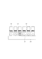
まず、前記第1及び第2の工程において、図1に示す様に、2乃至8インチのサファイア基板10を準備し、ストライプ状などのSiO2層13を形成する。図1(a)は断面図であり、図1(b)は上面図である。SiO2層13は、スパッタやCVD(SiH4を用いる)などで形成することができ、ここでは、これをストライプ状にエッチングする。例えば、SiO2層13のストライプの幅は数十μm、厚みは1μm以下、ストライプの間隔は数μmとする。これにより、サファイア基板10のストライプ状の露出部が形成される。同幅、同厚のストライプ状のSiO2層13を等間隔で形成することは、後述する窒化ガリウム系化合物半導体の平坦表面を形成するために重要である。
First, in the first and second steps, as shown in FIG. 1, a 2 to 8
次に、前記第3及び第4の工程において、断面図である図2(a)に示す様に、露出部を持つサファイア基板10上に、例えば、470℃の低温で厚み25nmの非晶質GaN15をMOCVD成長で堆積する。これは、例えば、サファイア基板10を支持するサセプター、ヒータ、反応ガス噴射管などを備える周知の反応容器内で行われる。Gaソースガスとしてトリメチルガリウム(TMG)を用い、水素ガスをキャリアとしてN源のアンモニアを反応ガス噴射管から基板表面に噴射する。続いて、断面図である図2(b)に示す様に、例えば、1100℃に昇温して非晶質GaN15を分断し、SiO2層13上の非晶質GaN15を蒸発させて、サファイア基板10の露出部上に非晶質GaNの核16を形成する。
Next, in the third and fourth steps, as shown in FIG. 2A which is a cross-sectional view, on the
次に、前記第5の工程において、TMGとアンモニアのソースガスを前記反応容器内に再導入する。そして、サファイア基板10上の核16のサイズ増大、合体、結晶成長、ファセット形成、転移線の屈曲(図3(a)参照)、SiO2層13上への横方向結晶成長、隣接する結晶粒同士の衝突、合体、転移網の形成、平坦表面形成(図3(b)参照)を行う。こうして、これらの過程を経て、サファイア基板10上に窒化ガリウム系化合物半導体のMOCVDエピタキシャル層20が形成される。エピタキシャル層20の膜厚は、SiO2層13のストライプの幅に一致し、ここでは、ほぼ数十μmである。窒化ガリウム系化合物半導体のエピタキシャル層は、MOCVDなどの気相成長法の他に、MBE法を利用して成長させることもできる。
Next, in the fifth step, TMG and ammonia source gas are reintroduced into the reaction vessel. Then, increase in size of the
次に、前記第6の工程において、図4の断面図に示す様に、サファイア基板10の露出部上の窒化ガリウム系化合物半導体のエピタキシャル層20を除去してトレンチすなわち分離溝25を形成する。分離溝25は、例えば、パターニングされたレジスト107のマスクを用いて、RIE(塩素系ガス)或いはレーザ・スクライバーによるトレンチ形成により形成することができる。この際、SiO2層13の端が露出される。このトレンチは、後述する選択エッチングのときのエッチング液の流路となる。通常の機械的なダイシング装置を用いてもこのトレンチは形成できるが、ウェーハ状態での移設は不可能である。しかし、このセグメントに分割された第2の基板からなるキャリアを多数個用意すれば、サファイア基板よりも大口径のシリコン基板、例えば、12インチ径基板への移設も、フリップチップボンダーを利用すれば可能となり、有用となる。
Next, in the sixth step, as shown in the cross-sectional view of FIG. 4, the gallium nitride compound
分離溝25を形成する目的を説明する。1つは上述のエッチング液流路の形成のためであるが、他の1つは、比較的欠陥密度の大きい部分を除くためである。GaNエピタキシャル層20における欠陥密度分布とLED効率の比較を示す図5を用いて説明する。図5(a)は本実施形態のGaNエピタキシャル層20を示し、図5(b)はサファイア基板上に全面的に成長させた従来のGaNエピタキシャル層を示す。また、図5(c)は、図5(a)、(b)において図示する各ゾーンA、B、C、Dの面積、欠陥密度、LED内部量子効率、LED外部効率、LED全体効率を比較して示す。図5(c)の表から分かる様に、図5(a)に示すゾーンCは結晶品質的に比較的劣るので、本発明ではこれを除いてゾーンA、Bをデバイス作製に使用するのである。これに伴い、前記分離溝25ができるので、これを利用してSiO2層13をエッチング犠牲層として用いてGaNエピタキシャル層を他の基板に移設する。このことで、高価なサファイア基板が再利用できる様になって、コストが抑制される。これと比較して、図5(b)に示す従来のものでは、本実施形態のゾーンBとほぼ等しい結晶品質のGaNエピタキシャル層が得られるが、サファイア基板を再利用できないので、コスト的には高価にならざるを得ない。
The purpose of forming the
次に、前記窒化ガリウム系化合物半導体層の形成方法で得られた第1の基板(サファイア基板など)上の窒化ガリウム系化合物半導体層を他の基板へ移設する本発明の移設方法の基本的な実施形態について説明する。この基本的な実施形態は、次の工程を少なくとも含む。
前記第1の基板上の第1の層の端部を表出させる第7の工程処理により分離可能状態となる分離層を表面に有し貫通溝が存在する第2の基板を用意する第8の工程。
分離層を介して第1の基板と第2の基板を貼り合わせる第9の工程。
貼り合わせた第1及び第2の基板をエッチング液(HF溶液)に浸潤してエッチング液を前記貫通溝と前記分離溝を通して第1の層と接触させることにより、第1の層を選択的にエッチングして第1の基板上のエピタキシャル層を第2の基板に移設する第10の工程。
第2の基板に移設されたエピタキシャル層の少なくとも一部を第3の基板に接合し、第2の基板とエピタキシャル層を前記分離層で分離してエピタキシャル層を第2の基板から第3の基板に移設する第11の工程。
Next, the basic method of the transfer method of the present invention is to transfer the gallium nitride compound semiconductor layer on the first substrate (such as a sapphire substrate) obtained by the method of forming the gallium nitride compound semiconductor layer to another substrate. Embodiments will be described. This basic embodiment includes at least the following steps.
Preparing a second substrate having a separation layer on its surface and having a through groove on its surface, which is made separable by a seventh step treatment for exposing an end portion of the first layer on the first substrate; Process.
A ninth step of bonding the first substrate and the second substrate through the separation layer;
The first and second substrates bonded together are infiltrated with an etching solution (HF solution), and the etching solution is brought into contact with the first layer through the through groove and the separation groove, thereby selectively selecting the first layer. A tenth step of transferring the epitaxial layer on the first substrate to the second substrate by etching;
At least part of the epitaxial layer transferred to the second substrate is joined to the third substrate, the second substrate and the epitaxial layer are separated by the separation layer, and the epitaxial layer is separated from the second substrate to the third substrate. An eleventh step of relocating.
前記第3の基板は、典型的には、シリコン基板であり、前記エピタキシャル層は第2の基板から第3の基板にウェーハスケールで、或いは部分的に移設される。また、本発明においては、上記シリコン基板以外の基板として金属基板を用いることもできる。以下に本発明において金属基板を用いる際の注意すべき点について説明する。電子デバイス、高周波トランジスタ、レーダ用、通信用の高出力アンプなどに使用するGaN系のHEMT(高電子移動度トランジスタ(High Electron Mobility Transistor))等は、大きな発熱がその素子特性を劣化させる。その為に、より高い熱伝導度が要求されるデバイスへの応用には、サファイアやシリコンよりも熱伝導度が高いSiCが使用される。そこで、本発明において上記基板に代替する安価な基板として、金属基板が考えられる。最も有効なのが、Cuであるが、GaNとの熱膨張係数を合わせこむ(熱膨張係数の差を一定の範囲内とする)ことが大切なので、W/Cuの合金が有効である。他の使用可能な金属材料としてはAl、W、Tiなどが挙げられる。しかし、熱伝導度については良好であっても、熱膨張係数の違いにより、デバイス製造時の熱処理工程やデバイスの発熱時にストレスが発生し、基板から剥離、離脱する場合がある。そのため、基板として用いるデバイスの製造時及び使用時を考慮して、熱膨張係数の整合と耐熱性との関係から最適な金属材料を選定することが重要となる。 The third substrate is typically a silicon substrate, and the epitaxial layer is transferred from the second substrate to the third substrate on a wafer scale or partially. In the present invention, a metal substrate can be used as a substrate other than the silicon substrate. Hereinafter, points to be noted when using a metal substrate in the present invention will be described. In a GaN-based HEMT (High Electron Mobility Transistor) used for an electronic device, a high-frequency transistor, a high-power amplifier for radar, communication, and the like, a large amount of heat deteriorates its element characteristics. For this reason, SiC having higher thermal conductivity than sapphire or silicon is used for application to devices that require higher thermal conductivity. Therefore, a metal substrate is conceivable as an inexpensive substrate that replaces the substrate in the present invention. The most effective is Cu, but it is important to match the thermal expansion coefficient with GaN (the difference in thermal expansion coefficient is within a certain range), so an alloy of W / Cu is effective. Other usable metal materials include Al, W, Ti, and the like. However, even if the thermal conductivity is good, due to the difference in thermal expansion coefficient, stress may be generated during the heat treatment process during device manufacture or during device heat generation, and may be detached from the substrate. For this reason, it is important to select an optimal metal material from the relationship between the thermal expansion coefficient matching and the heat resistance in consideration of the manufacturing and use of the device used as the substrate.
前記第8乃至第11の工程について、詳しく説明する。
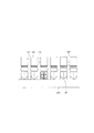
前記第7の工程は、図4を用いて説明した前記第6の工程と実質的に同じものである。次に、前記第8の工程において、第2の基板である例えば転写ウェーハ(Si)100を用意し、図6と図7に示す様に、これに貫通溝(エッチング流路)150を形成する。また、転写ウェーハ100の一面に、前記分離層である例えば両面接着シート115を設置し、図6(b)に示す様に、これにも孔を形成して貫通溝150と連結させる。貫通溝150は、サンドブラスト(ウェーハ100の厚さが50μm以上の場合に適する)、レーザ・スクライバー(同じく40μm以上の場合に適する)、RIE(ボッシュプロセス)(同じく40μm以下の場合に適する)などで形成できる。両面接着シート115の孔は、レーザ加工などで形成できる。両面接着シート115は、例えば熱剥離粘着層、光剥離粘着層などを含む。ここで、光剥離粘着層は、光の照射により分解又は結合強度が低下する材料を含む層であり、熱剥離粘着層は、加熱又は冷却により分解又は結合強度が低下する材料を含む層である。
The eighth to eleventh steps will be described in detail.
The seventh step is substantially the same as the sixth step described with reference to FIG. Next, in the eighth step, for example, a transfer wafer (Si) 100 as a second substrate is prepared, and a through groove (etching flow path) 150 is formed in this as shown in FIGS. . Further, for example, a double-
次に、前記第9の工程において、両面接着シート115を介して、レジスト107でカバーされたストライプ状のGaNエピタキシャル層20を持つ第1の基板(サファイア基板10)と第2の基板(転写ウェーハ100)を貼り合わせる。この状態における転写ウェーハ100の貫通溝150とストライプ状のGaNエピタキシャル層20の配置関係が図7に示されている。また、断面の様子が図8に示されている。
Next, in the ninth step, a first substrate (sapphire substrate 10) having a striped
前記第10の工程において、こうして貼り合わせた第1の基板(サファイア基板10)と第2の基板(転写ウェーハ100)をエッチング液(HF溶液)に浸潤し、エッチング液を貫通溝150と分離溝(トレンチ)25を通して第1の層13と接触させる。このことにより、図9に示す様に、第1の層(SiO2層)13が選択的にエッチングされ、サファイア基板10上のエピタキシャル層20が転写ウェーハ100に移設される。このとき、HF溶液に関して、GaNなどの窒化ガリウム系化合物半導体はSiO2に対して無限大のエッチング選択性を持つので、SiO2層13が完全に、選択的にエッチングされる。エッチング液の濡れ性向上のために、エッチング液に界面活性剤を混入するとエッチング速度を増加させるために、効果的である。分離されたサファイア基板10は、成長基板として再使用することができる。これにより、高価なサファイアウェーハが再利用できて、窒化ガリウム系化合物半導体層の製造コストが下げられることになる。サファイア基板は、Si基板やGaAs基板などよりも堅牢で耐熱性も高く、安定であるので、リサイクルに耐えることができる。サファイア(Al2O3)の融点が2050℃であるのに対して、Siの融点とGaAsの融点は夫々1420℃、1238℃である。また、アルミニウムと酸素原子の結合は強固で、GaAsのように、Asが選択的に抜けたりはせず、極めて熱的にも堅牢で、又、腕時計の窓ガラスに使用されることからも判るように、機械的にも堅牢である。
In the tenth step, the first substrate (sapphire substrate 10) and the second substrate (transfer wafer 100) bonded in this manner are infiltrated into an etching solution (HF solution), and the etching solution is passed through the through
次に、前記第11の工程を説明する。ここでは、第2の基板(転写ウェーハ100)に移設されたエピタキシャル層20を第3の基板(Siウェーハ200)に接合し、第2の基板とエピタキシャル層を分離層115で分離してエピタキシャル層を第2の基板から第3の基板に移設する。エピタキシャル層20は、ウェーハスケールで移設することもできるし、その一部を選択的に移設することもできる。まず、ウェーハスケールで移設する場合について説明する。
Next, the eleventh step will be described. Here, the
図10は、分子間力(ファンデル・ワールス力)接合でエピタキシャル層20をシリコンウェーハ(第3の基板)200に直接接合する例を示す。この場合、シリコンウェーハ200に対してアルゴン、酸素、窒素などのプラズマ活性種を用いて、表面プラズマ活性化処理を施すことが、接合力を高める上で有効である。エピタキシャル層20をLEDに応用する場合には、光取り出し効率向上のために、例えば、シリコン基板200とGaN−LED層の界面にSiO2(これは屈折力を変化させる)や反射層を挿入すると効果的である。この場合、タック性(粘着性・密着性)の制御が容易な有機絶縁層(スピンオンポリマー:Spin−on Polymer)が有効に働く上、500℃以下の低温で十分に強固な接合を実現できる。エピタキシャル層20をシリコンウェーハ200へ直接接合する場合に、500℃以上の熱処理により共有結合を形成して接合力をより高めることができる。
FIG. 10 shows an example in which the
分離層115が熱剥離粘着層を含む場合、第2の基板100とエピタキシャル層20を分離層で分離することは、図11に示す様に、分離層115を100℃以上に加熱して行う。これにより、熱剥離粘着層内の発泡で転写Siウェーハ100が分離される。アッシャー等でレジスト107を剥離して第2の基板100とエピタキシャル層20を分離することもできる。こうして分離された貫通溝150を持つSiウェーハ100は、サファイア基板10と同様に、残留した分離層(両面シート)115を剥離後に転写ウェーハとして再利用することができる。このことも、窒化ガリウム系化合物半導体層の製造コストを下げることに寄与する。
When the
以上の様にして、前記窒化ガリウム系化合物半導体層の形成方法で得られた窒化ガリウム系化合物半導体層が接合されたシリコン基板を得ることができる。得られた窒化ガリウム系化合物半導体のエピタキシャル層20は、青色(蛍光白色)縦型・固体照明LEDなどを作製するのに用いることができる。エピタキシャル層20を何の作製に用いるかに応じて、図3に示す結晶作成過程の適宜の時間において、ソースガスが適宜変更されたり適切な不純物が導入されたりする。これらについては後で詳しく述べる。
As described above, a silicon substrate to which the gallium nitride compound semiconductor layer obtained by the method for forming a gallium nitride compound semiconductor layer is bonded can be obtained. The obtained
前述した様に、前記第11の工程において、エピタキシャル層20の一部を選択的に移設することもできる。この場合は、前記エピタキシャル層20の一部と、第3の基板200上のエピタキシャル層が移設される領域との、少なくとも一方に所定の厚さの有機絶縁層などの接合層を設け、エピタキシャル層の一部と第3の基板とを接合層により接合する。そして、第3の基板200に接合層で接合されたエピタキシャル層20の一部のみを、第2の基板100から分離層115で分離する。
As described above, in the eleventh step, a part of the
これらの工程の例について説明する。選択的に移設される第1の機能性領域101(以下の説明では、前記エピタキシャル層20の一部をこの様にも呼ぶ)と、第3の基板200上の第1の機能性領域101が移設される領域との、少なくとも一方に所定の厚さの接合層205を設ける。本例では、図12に示す様に、駆動回路を備えるシリコン基板である第3の基板200上に接合層205を設ける。設け方としては、まず、図12(a)に示す様に第3の基板200上に、所定の厚さの接合層(有機絶縁層)205を形成し、その上の第1の機能性領域101の移設予定領域のみに対してレジスト206でマスキングを行う。化学的なウェットエッチング或いはRIEでドライエッチングを行い、図12(b)に示す様に所望の領域のみに接合層205を設け、レジスト206をアッシャーなどで剥離する。ここでは、接合層205の厚さは2.0μm程度とし(図12等では1.97μmと表示している)、その表面は充分に滑らかにする。この程度の厚さがあれば、第1の機能性領域101と接合層205を接合するときに、別の第2の機能性領域102が基板200の表面に強く押し付けられることは防止できる。この接合層の厚さとしては1.0μm〜10μm程度が好ましい。1.0μm以下の厚さになると前記効果が小さくなり、また10μm以上になると、機能性領域を移設した後に、当該機能性領域と基板に形成された回路等とを金属配線で、電気的に結合する際に段切れ等の問題が起こる可能性が高くなる。この際、図12(b)に示す様に、第1の機能性領域101以外の領域に対応する第3の基板200上の領域の表面に所定の凹凸208を形成してもよい。こうすれば、第2の機能性領域102と基板200の表面との接合がより確実に防止できる。凹凸208は、接合層(有機絶縁層)205を形成するときにオーバーエッチングなどを行うことで形成できる。凹凸208の面は、接合層205の表面より充分に粗いものである。例えば、接合層205の表面の滑らかさは、Rpv(凹凸のピークと谷の差の最大値)が2nm程度以下であり、Ra(凹凸のピークと谷の差の平均値)が0.2nm程度以下とする。一方、凹凸208の面の粗さは、Rpv(凹凸のピークと谷の差の最大値)が2nm程度以上であり、Ra(凹凸のピークと谷の差の平均値)が0.2nm程度以上とする。
Examples of these steps will be described. A first functional region 101 (a part of the
この様に、分離層115を有する第2の基板100の前記分離層の上には、島状ないしストライプ状に複数の前記エピタキシャル層20があり、これは、第1の機能性領域101以外に第2の機能性領域102を含んでいる。そして、本例では、少なくとも、第2の基板100上に残存することになる第1の機能性領域以外の第2の機能性領域102に対応する第3の基板200上の領域の表面に、所定の凹凸208を形成する。
As described above, the plurality of
本例において、接合層205は、例えば有機材料からなる膜である。有機材料からなる膜としては、ポリイミドなどの有機絶縁膜がある。ポリイミド以外にも、エポキシ系接着層などを使用することもできる。また、絶縁膜としては、上述の有機材料膜のみならず、酸化シリコン膜などの無機系の絶縁性の酸化膜を用いることもできる。例えば、第3の基板200としてのシリコン基板上及び/または内部を利用して回路領域を設ける場合には、次の様にしてもよい。スピンオングラス(SOG)を利用して、前記回路領域上の平坦性を上げるための酸化シリコン絶縁膜(これは粘着性を有する)を所定の厚さで第3の基板200上に形成し、これをパターニングしてもよい。有機絶縁層は可塑性が付与されるため、数ミクロンまで厚く塗布することができ、無機SOGよりもプロセス自由度が増加する。無機、有機SOGのタック性(粘着性)は、そのプリベーク温度を調節することにより、シラノール基やアルコキシ基などの加水分解性基の作用を制御することで、付与することが可能である。その後に硬化熱処理を施すと、比較的低温(五百℃以下)で強固な接合を実現できる。
In this example, the
上述した様に、第3の基板200は、例えば、半導体基板やシリコン基板、表面に酸化層が形成されているシリコンウェーハ、所望の電気回路(例えば、ドライバ回路)が設けられているシリコンウェーハなどである。ここでいうドライバ回路とは、例えば、発光ダイオード(LED)が前記化合物半導体多層膜を含み構成される場合に、当該LEDを1つまたは複数個のアレイ状に形成されたLEDアレイを駆動・制御するための回路のことである。シリコン基板は、いわゆるCZウェーハは勿論、表面にエピタキシャルシリコン層を有する基板であってもよく、またシリコン基板の代替としてSOI基板を用いることもできる。
As described above, the
次に、第1の機能性領域101と第3の基板200とを接合層205により接合する工程と、第2の基板100と第1の機能性領域101とを分離層115で分離する工程について説明する。図13(a)に示す様に、第2の基板100の分離層115上の第1の機能性領域101と接合層205をアライメントして接合し、図13(b)に示す様に、第2の基板100と第1の機能性領域101とを分離層115で分離する。ここでは、分離層115としては、シート基材115cの一面にUV剥離粘着層115aを持ち他面に熱剥離粘着層115bを持つ両面接着シートを用いるとする。また、後の工程のために、第2の機能性領域102が存在する領域に対応する第2の基板100の表面には、遮光層117が設けられる。遮光層117は蒸着などで形成することができるが、容易に剥がせるステンシルマスクを用いることもできる。
Next, a step of bonding the first
分離層115で分離するために、透明基板100の側からUV光を照射して分離層115のUV剥離粘着層の分解或いは結合強度の弱化をもたらす。このことで、第2の基板100と第1の機能性領域101とを分離する。遮光層117があるので、第2の機能性領域102の部分の分離層115にはUV光が照射されず、これはそのままで、図13(b)に示す様に、第2の機能性領域102は第2の基板100側に残って移設されない。この様に、本例では、第2の基板100は透光層117を有し、分離層115は光の照射により分解又は結合強度が低下する材料からなるUV剥離粘着層を含む。そして、少なくとも第1の機能性領域101と第2の基板100との間の分離層115に光の照射を行って、第2の基板100と第1の機能性領域101を分離層115で分離する。
In order to separate by the
全体的に光の照射を行って、第2の基板100と第1の機能性領域101を分離層115で分離することもできる。全体的に光の照射をすれば、分離層115のUV剥離粘着層は全体的に分解或いは結合強度が弱化して、接合層205と接合した第1の機能性領域101はその接合力で第2の基板100から分離される。このとき、第3の基板200と接合していない第2の機能性領域102の部分でも、分離層115のUV剥離粘着層の粘着力は低下している。しかし、第2の機能性領域102の部分には第3の基板200側から引き剥がし力が働かないので、第2の機能性領域102は第2の基板100側に残ることになる。この方法は、多少確実性が低下するが、遮光層を設けなくてもよく、光の照射も単純に行えばよいので、簡易に行うことができる。この場合も、分離層115の弱った粘着力のUV剥離粘着層により第2の基板100側に残った第2の機能性領域102の部分を、次に説明する様に更に他の基板に移設することができる。
It is also possible to separate the
分離層115は、前記構成のものに限られない。分離層115は、一層のUV又は熱の剥離粘着層などであってもよいし、UV剥離粘着層115aと熱剥離粘着層115bの配置が図示例とは逆転したシートであってもよい。また、図15に示す様に、第1及び第2の機能性領域101、102に夫々対応して異なる特性を持つ分離層120、121を第2の基板100上に設けることもできる。例えば、一方がUV剥離粘着層で、他方が熱剥離粘着層という組み合わせがある。また、一方が第1の光剥離粘着層で、他方が第2の光剥離粘着層(これは第1の光剥離粘着層とは異なる波長の光で分解或いは結合強度が弱化する粘着層)という組み合わせがある。更には、一方が第1の熱剥離粘着層で、他方が第2の熱剥離粘着層(これは第1の熱剥離粘着層とは異なる温度で分解或いは結合強度が弱化する粘着層)という組み合わせもある。分離層115は、シートではなく、第2の基板100上に塗布、蒸着などで形成することもできる。具体的な材料としては、リバアルファ(日東電工製の商品名)がある。また、UV剥離粘着材料としては、ダイシングテープに用いられているものがあり、熱剥離粘着材料としては、熱発泡カプセルを含有するものがある。
The
第2の機能性領域102を更に他の基板に移設する場合は、第1の機能性領域101の移設とほぼ同様のことを行えばよい。すなわち、図14(a)に示す様に、第4の基板300上に接合層(有機絶縁層)305を形成し、その上の第2の機能性領域102の移設予定領域のみにレジストでマスキングを行う。そして、化学的なエッチング或いはRIEでエッチングを行い、所望の領域のみに接合層305を設ける。次に、図14(a)に示す様に、第2の機能性領域102と接合層305をアライメントして接合し、図14(b)に示す様に、第2の基板100と第2の機能性領域102とを分離層115で分離する。ここでは、図14(b)に示す様に、170℃程度に加熱して分離層115の熱剥離粘着層115bの分解或いは結合強度の弱化をもたらすことで、第2の基板100と第2の機能性領域102とを分離している。
When the second
ここで、図14の工程が最後の移設工程である場合、この工程では、第1及び第2の機能性領域101、102を形成するときに用いたレジスト107をアッシャーなどで剥離して、第2の基板100と第2の機能性領域102とを分離することもできる。また、本例において、熱剥離粘着層のみを有する分離層115を用いた場合、遮光層117は不必要で、図13の工程では、第1の機能性領域101に対応する部分の分離層115を局所的に加熱することになる。分離温度の差が一定以上ある熱剥離粘着層を面内に図15で示す様にパターニングして設ければ、より精度良く選択的に分離できる。
Here, when the process of FIG. 14 is the last transfer process, in this process, the resist 107 used when forming the first and second
前述した様に、分離層115のUV剥離粘着層115aと熱剥離粘着層115bの配置を図13に示すものとは反対にすることもできる。こうしたとき、例えば、遮光層117は不必要で、図13の工程では、第1の機能性領域101に対応する部分の分離層115を局所的に加熱する。そして、図14の工程では、透明基板100の側からUVを照射して分離層115のUV剥離粘着層の分解或いは結合強度の弱化をもたらすことで、第2の基板100と第2の機能性領域102とを分離する。
As described above, the arrangement of the UV peeling
この様に、第2の機能性領域102を更に他の基板に移設したい場合は、第2の基板に残存する第2の機能性領域と、第4の基板上の第2の機能性領域が移設される領域との、少なくとも一方に所定の厚さの接合層を設ける。そして、第2の機能性領域102と第4の基板300とを接合層305により接合する工程と、第2の基板100と第2の機能性領域102とを分離層115で分離する工程を更に実行する。この場合も、図14に示す様に、第4の基板300上の、少なくとも、第2の基板100上の第2の機能性領域102に対応する領域以外の領域の表面に、所定の凹凸308を形成してもよい。
As described above, when the second
本例によれば、前述の如き所定の厚さの接合層を用いるので、1つの基板に設けられた複数の窒化ガリウム系化合物半導体層のうち、任意の領域を選択的に別の基板に確実に移設することができる。例えば、第2の基板に高密度に配置した窒化ガリウム系化合物半導体層の一部を、歩留まりを低下させること無く他の基板に移設することができる。 According to this example, since the bonding layer having a predetermined thickness as described above is used, an arbitrary region of a plurality of gallium nitride-based compound semiconductor layers provided on one substrate can be selectively attached to another substrate. Can be relocated. For example, part of the gallium nitride-based compound semiconductor layer arranged on the second substrate at a high density can be transferred to another substrate without reducing the yield.
以下、シリコン基板上の窒化ガリウム系化合物半導体層を加工して作製されるLEDなどのデバイスに係る実施例、LEDアレイに係る実施例、LEDプリンタヘッドに係る実施例、及びLEDプリンタに係る実施例を詳細に説明する。 Examples of devices such as LEDs manufactured by processing a gallium nitride compound semiconductor layer on a silicon substrate, examples of LED arrays, examples of LED printer heads, and examples of LED printers Will be described in detail.
(第1の実施例)
第1の実施例は、本発明の移設方法によりSi基板上に移設された窒化ガリウム系化合物半導体のエピタキシャル層20を用いたデバイスである青色(蛍光白色)縦型・固体照明LEDに関する。このLEDの素子構造は、図16の断面図に示す如く次の様になっている。デバイス表面より、ITO透明電極410、p型GaNコンタクト層412、InGaN多重量子井戸型活性層414、n型GaNコンタクト層416、n+−低抵抗Si基板200、裏面Al電極418が配されている。
(First embodiment)
The first embodiment relates to a blue (fluorescent white) vertical / solid state lighting LED which is a device using an
こうしたエピタキシャル層20の構造は、前述の図3の形成工程において適宜に反応容器内の温度、ソースガスなどを変化させて作製される。例えば、多重量子井戸型活性層414とp型GaNコンタクト層412は次の様な工程で第1の基板10上に作製される。まず、成長温度840℃でIn0.02Ga0.98N障壁層を形成し、続けて3nm厚のIn0.15Ga0.85N井戸層、9nm厚のIn0.02Ga0.98N障壁層を交互に5層ずつ形成する。次に、成長温度を1000℃として、200nm厚のMgドープのp型GaN層412を形成する。図16の構造は、こうして作製されたエピタキシャル層20がSi基板200に移設された状態を示す。ソースガスとしては、GaNを形成するときにはトリメチルガリウム(TMG)を用い、InGaNを形成するときにはトリメチルインジウム(TMIn)をも用いる。また、GaAlNを形成する必要があるときには、トリメチルアルミニウム(TMAl)をも用いればよい。
Such a structure of the
本実施例のLEDの素子構造は、従来のサファイア基板上のLEDと比較して、次の様な特徴を有する。
基板裏面電極418が形成可能となり、表面側電極410の数が半減するので、デバイスの発光領域を拡大することができる。
取り出し効率向上のために、貼り合わせ技術により、屈折率変化を目的にしたSiO2や、反射ミラー(Al、Ag等)を基板200界面に挿入することが可能である。
機械的、熱的に安定なサファイア基板(第1の基板10)を再利用できることから、大きな製造コスト減が期待される。
The element structure of the LED of this embodiment has the following characteristics as compared with a conventional LED on a sapphire substrate.
The substrate back
In order to improve the extraction efficiency, it is possible to insert SiO 2 for the purpose of changing the refractive index or a reflection mirror (Al, Ag, etc.) at the interface of the
Since a mechanically and thermally stable sapphire substrate (first substrate 10) can be reused, a great reduction in manufacturing cost is expected.
(第2の実施例)
第2の実施例は、本発明の移設方法によりSi基板上に移設された窒化ガリウム系化合物半導体のエピタキシャル層20を用いたデバイスである電子写真用などの青色LED固体スキャナーである。素子構造(LED/CMOSドライバ回路)は、図17に示す如く、次の様になっている。デバイス表面より、Au/Niのp側電極510、p型GaNコンタクト層512、InGaN量子井戸型活性層514、n型GaNコンタクト層516、Au/Niのn側電極518、CMOSドライバ回路内蔵のSi基板200が配されている。
(Second embodiment)
The second embodiment is a blue LED solid state scanner for electrophotography or the like, which is a device using the
ここでは、ドライバIC(駆動回路)とLED素子とが接続されている。図17の構成において、ドライバICを構成するMOSトランジスタ560を含むシリコン基板200上に、有機材料からなる絶縁膜520(図13等の接合層205参照)が設けられている。そして、絶縁膜520上に、窒化ガリウム系化合物半導体多層膜からなるLED発光領域570が設けられている。また、図17において、580は絶縁膜、550は、MOSトランジスタ560のソース又はドレイン領域となるワイヤボンディングパッドである。こうした構成は、例えば、図13の第3の基板200の構成から作製することができる
Here, the driver IC (drive circuit) and the LED element are connected. In the configuration of FIG. 17, an insulating film 520 (refer to the
本実施例のLEDの素子構造は、従来のGaAs基板上の赤外LED(波長760nm)と比較して、次の様な特徴を有する。
従来、赤外領域の波長(750nm)の電子写真用の光源として、レーザやLEDが使用されているが、波長が半減する青色領域の光源を用いると、スポットサイズが半減する。すなわち、波長450nm程度とすれば、True2400dpiに相当する10μmφのスポットサイズを実現することができる。
LEDアレイの駆動回路が下地シリコンに内蔵されているため、ボンディングワイヤ数が大幅に減少し、ヘッドユニット全体のコストは大きく削減される。
機械的、熱的に安定なサファイア基板を再利用できることから、大きな製造コスト減が期待される。また、移設後の基板上の窒化ガリウム系化合物半導体層の密度と高密度に第2の基板上に配置した窒化ガリウム系化合物半導体層の密度の比を1:nとする選択的な移設方法を用いれば、成長基板を有効に使用できて、更なるコスト減が期待できる。このコスト減は、基板の再利用と併せて、一枚の基板から複数の活性層を移設することができる相乗効果からも期待できる。
The element structure of the LED of this embodiment has the following characteristics as compared with a conventional infrared LED (wavelength 760 nm) on a GaAs substrate.
Conventionally, lasers and LEDs have been used as light sources for electrophotography having a wavelength in the infrared region (750 nm). However, if a light source in the blue region whose wavelength is halved is used, the spot size is halved. That is, if the wavelength is about 450 nm, a spot size of 10 μmφ corresponding to True 2400 dpi can be realized.
Since the drive circuit for the LED array is built in the underlying silicon, the number of bonding wires is greatly reduced, and the cost of the entire head unit is greatly reduced.
Since a mechanically and thermally stable sapphire substrate can be reused, a significant reduction in manufacturing cost is expected. And a selective transfer method in which the ratio of the density of the gallium nitride compound semiconductor layer on the transferred substrate and the density of the gallium nitride compound semiconductor layer disposed on the second substrate is 1: n. If used, the growth substrate can be used effectively, and further cost reduction can be expected. This cost reduction can be expected from a synergistic effect that allows a plurality of active layers to be transferred from one substrate together with the reuse of the substrate.
(第3の実施例)
第3の実施例は、本発明の移設方法によりSi基板上に移設された窒化ガリウム系化合物半導体のエピタキシャル層20を用いたデバイスであるGaNトランジスタ(HEMT、MIS)である。素子構造は、図18に示す如く、次の様になっている。表面より、Alゲート電極610、SiO2絶縁層612、無添加AlGaN活性層614、Ti/Alソース電極616、N+ソース領域618(Siイオン注入)618、i−GaN層620、n+低抵抗Si基板200、裏面Al電極622が配されている。
(Third embodiment)
The third embodiment is a GaN transistor (HEMT, MIS) which is a device using an
本実施例の素子構造は、従来のサファイア基板上のLEDと比較して、次の様な特徴を有する。
基板裏面電極622が形成可能となり、デバイス層の電位が浮遊せずに、確定、制御でき、素子動作の安定性、信頼性が向上する。
下地Si基板200に作製したシリコン回路(CMOS、バイポーラ、高耐圧FETなど)を内蔵、接続することができる。
機械的、熱的に安定なサファイア基板を再利用できることから、大きなコスト減が期待される。
Si上の直接成長GaN/Siよりも、欠陥密度を低減できて、デバイスの特性、信頼性、均一性、収率が向上できる。GaN−HEMTは従来のGaAs−HEMTに比較して、数ギガヘルツのC帯域において、高い出力の増幅器を実現でき、携帯電話基地局や衛星通信、レーダ送信機の小型化、省電力化に貢献できる。
The element structure of the present embodiment has the following characteristics as compared with a conventional LED on a sapphire substrate.
The substrate back
A silicon circuit (CMOS, bipolar, high voltage FET, etc.) fabricated on the
Because a mechanically and thermally stable sapphire substrate can be reused, a significant cost reduction is expected.
Defect density can be reduced and device characteristics, reliability, uniformity, and yield can be improved as compared with directly grown GaN / Si on Si. Compared with conventional GaAs-HEMT, GaN-HEMT can realize high output amplifier in C band of several gigahertz, and can contribute to miniaturization and power saving of mobile phone base station, satellite communication, radar transmitter. .
(第4の実施例)
前述の窒化ガリウム系化合物半導体層の形成方法及び移設方法を用いて製造されるLEDアレイの実施例を説明する。前記実施形態において説明した形成方法及び移設方法を用いることにより、図19に示す様なLEDアレイが提供される。図19は、プリント基板5000上に駆動回路とLEDアレイ4000とが接続・配置された一構成例を示す斜視図である。駆動回路とLEDアレイは、前述した窒化ガリウム系化合物半導体層の移設方法で図13等に示す様にシリコン基板上に複数のLED素子を形成し、シリコン基板をダイシングにより分割して得たものを複数並べることで得られる。各LED素子と駆動回路の断面構成は、図17のLED発光領域を含むLED素子と駆動回路と同じ様なものである。
(Fourth embodiment)
An embodiment of an LED array manufactured by using the above-described gallium nitride compound semiconductor layer formation method and transfer method will be described. By using the formation method and the transfer method described in the above embodiment, an LED array as shown in FIG. 19 is provided. FIG. 19 is a perspective view showing a configuration example in which the drive circuit and the
図19の構成では、複数のLEDアレイ/駆動回路4000をプリント基板5000上にライン状に並べている。LEDアレイ/駆動回路4000の各LED素子とドライバICの駆動素子は図17に示す様に電気的に接続されている。必要に応じて、ライン状に配されたLEDアレイ4000に、ロッドレンズアレイ(例えば、SLA:セルフォックレンズアレイ)3000を実装することにより、LEDプリンタヘッドとすることができる。ライン状に配されたLEDアレイ4000から放出された光はロッドレンズアレイ3000で集光され、LEDアレイ結像が得られる。本発明においては前記ロッドレンズアレイに替えてマイクロレンズアレイを用いることもできる。
In the configuration of FIG. 19, a plurality of LED arrays /
シリコン基板上に金属膜かDBRミラーを介してLED素子構成層が設けられている場合には、その指向性の向上により、更に微細なスポットサイズが実現される。従って、ロッドレンズアレイは省略して、LEDプリンタヘッドとすることもできる。 When the LED element constituent layer is provided on the silicon substrate via a metal film or a DBR mirror, the finer spot size is realized by improving the directivity. Therefore, the rod lens array can be omitted and an LED printer head can be obtained.
マトリックス駆動する際の一例を、図20に示す。図20は、電極数を減らすための時分割駆動可能な発光素子アレイ回路8500を示す図である。図20において、8011はn側電極、8017はp側電極、8021はn型GaN上の絶縁膜、8022はp型GaNコンタクト層上の絶縁膜、8023は発光領域である。
An example of matrix driving is shown in FIG. FIG. 20 shows a light-emitting
本発明の窒化ガリウム系化合物半導体層の形成方法及び移設方法を用いることで、低コストで高性能な上記の如きLEDアレイ、LEDプリンタヘッドを提供することができる。 By using the method for forming and transferring the gallium nitride compound semiconductor layer of the present invention, it is possible to provide the LED array and the LED printer head as described above, which are low-cost and high-performance.
(第5の実施例)
第4の実施例で説明したLEDプリンタヘッドを用いて、LEDプリンタを構成した例を図21(a)に示す。このLEDプリンタは、前記LEDプリンタヘッドと、感光ドラムと、帯電器とを備え、LEDプリンタヘッドを光源として、感光ドラムに静電潜像を書き込む作像ユニットを含む。
(Fifth embodiment)
FIG. 21A shows an example in which an LED printer is configured using the LED printer head described in the fourth embodiment. The LED printer includes the LED printer head, a photosensitive drum, and a charger, and includes an image forming unit that writes an electrostatic latent image on the photosensitive drum using the LED printer head as a light source.
LEDプリンタの構成例を示す概略断面図である図21(a)において、プリンタ本体8100の内部には、時計廻りに回転する感光ドラム8106が収納されている。感光ドラム8106の上方には、感光ドラムを露光するためのLEDプリンタヘッド8104が設けられている。LEDプリンタヘッド8104は、画像信号に応じて発光する複数の発光ダイオードが配列されたLEDアレイ8105と、各々の発光ダイオードの発光パターンを感光ドラム8106上に結像させるロッドレンズアレイ8101とから構成される。ここで、ロッドレンズアレイ8101は、先に説明した実施例に示す構成を有している。ロッドレンズアレイ8101により、発光ダイオードの結像面と感光ドラム8106の位置は一致する様になっている。つまり、発光ダイオードの発光面と感光ドラムの感光面とは、ロッドレンズアレイによって光学的に共役関係とされている。
In FIG. 21A, which is a schematic sectional view showing a configuration example of an LED printer, a
感光ドラム8106の周囲には、感光ドラム106の表面を一様に帯電させる帯電器8103、及びプリンタヘッド8104による露光パターンに応じて感光ドラム8106にトナーを付着させてトナー像を形成する現像器8102が設けられている。また、感光ドラム8106上に形成されたトナー像をコピー用紙等の不図示の被転写材上に転写する転写帯電器8107、及び転写後に感光ドラム8106上に残留しているトナーを回収するクリーニング手段8108も設けられている。
Around the
更に、プリンタ本体8100には、前記被転写材を積載する用紙カセット8109、用紙カセット8109内の被転写材を感光ドラム8106と転写帯電器8107との間に供給する給紙手段8110が設けられている。また、転写されたトナー像を被転写材に定着させるための定着器8112、被転写材を定着器8112に導く搬送手段8111、及び定着後に排出された被転写材を保持する排紙トレイ8113が設けられている。
Further, the printer
次に、前記LEDプリンタヘッドと、感光ドラムと、帯電器と、LEDプリンタヘッドを光源として感光ドラムに静電潜像を書き込む作像ユニットとを複数備えるカラーLEDプリンタを説明する。図21(b)に、カラーLEDプリンタの一構成例の機構部の概略構成図を示す。図21(b)において、9001、9002、9003、9004はそれぞれマゼンタ(M)、シアン(C)、イエロー(Y)、ブラック(K)の各感光体ドラム、9005、9006、9007、9008は各LEDプリンタヘッドである。9009は、転写紙を搬送すると共に各感光体ドラム9001、9002、9003、9004に接触するための搬送ベルトである。9010は給紙用のレジストローラ、9011は定着ローラである。また、9012は、搬送ベルト9009に転写紙を吸着保持するためのチャージャー、9013は除電チャージャー、9014は転写紙の先端検出用センサである。
Next, a color LED printer including a plurality of LED printer heads, a photosensitive drum, a charger, and an image forming unit that writes an electrostatic latent image on the photosensitive drum using the LED printer head as a light source will be described. FIG. 21B is a schematic configuration diagram of a mechanism unit of one configuration example of the color LED printer. In FIG. 21B, 9001, 9002, 9003, and 9004 are magenta (M), cyan (C), yellow (Y), and black (K) photosensitive drums, respectively, 9005, 9006, 9007, and 9008 are each. LED printer head.
本発明の窒化ガリウム系化合物半導体層の形成方法及び移設方法を用いることで、低コストで高性能な上記の如きLEDプリンタを提供することができる。 By using the method for forming a gallium nitride compound semiconductor layer and the transfer method of the present invention, it is possible to provide the above-described LED printer having high performance at a low cost.
本発明は、半導体基板上にアレイ状に窒化ガリウム系化合物の半導体素子を配置したアレイ素子に適用することができる。特に、半導体基板上に配置された窒化ガリウム系化合物半導体層を含むLED素子を用いたLEDプリンタやディスプレイなどの表示装置、或いは、光送受信用素子や受光素子などに適用することができる。受光素子に適用すれば、スキャナーを構成することもできる。 The present invention can be applied to an array element in which gallium nitride compound semiconductor elements are arranged in an array on a semiconductor substrate. In particular, the present invention can be applied to a display device such as an LED printer or a display using an LED element including a gallium nitride compound semiconductor layer disposed on a semiconductor substrate, an optical transmission / reception element, a light receiving element, or the like. If applied to a light receiving element, a scanner can also be configured.
10 第1の基板(サファイア基板、SiC基板)
13 第1の層(SiO2層、エッチング犠牲層)
15 非晶質窒化ガリウム系化合物半導体
16 非晶質窒化ガリウム系化合物半導体の核
20 窒化ガリウム系化合物半導体層(エピタキシャル層)
25 分離溝
100 第2の基板
101 第1の機能性領域
102 第2の機能性領域
115 分離層
150 貫通溝
200 第3の基板
205、305 接合層
3000 ロッドレンズアレイ
4000、8105 LEDアレイ
8104、9005、9006、9007、9008 LEDプリンタヘッド
10 First substrate (sapphire substrate, SiC substrate)
13 First layer (SiO 2 layer, etching sacrificial layer)
15 Amorphous gallium
25
Claims (10)
前記第1の基板上の第1の層の端部を表出させる工程と、
処理により分離可能状態となる分離層を表面に有し貫通溝が存在する第2の基板を用意する工程と、
前記分離層を介して前記第1の基板と前記第2の基板を貼り合わせる工程と、
前記貼り合わせた第1の基板と第2の基板をエッチング液に浸潤してエッチング液を前記貫通溝と前記分離溝を通して前記第1の層と接触させることにより、前記第1の層を選択的にエッチングして前記第1の基板上の前記エピタキシャル層を前記第2の基板に移設する工程と、
前記第2の基板に移設された前記エピタキシャル層の少なくとも一部を第3の基板に接合し、前記第2の基板と前記エピタキシャル層を前記分離層で分離して前記エピタキシャル層を前記第2の基板から前記第3の基板に移設する工程と、
を含むことを特徴とする移設方法。 A method of forming a gallium nitride-based compound semiconductor layer by epitaxially growing a gallium nitride-based compound semiconductor on a first substrate that is a sapphire substrate or a SiC substrate, wherein the gallium nitride-based compound semiconductor layer is mainly formed on the first substrate. Forming a first layer comprising: removing the first layer partially to form an exposed portion of the first substrate; and on the first substrate having the exposed portion, Depositing an amorphous gallium nitride compound semiconductor; evaporating the amorphous gallium nitride compound semiconductor on the first layer; and exposing the amorphous gallium nitride on the exposed portion of the first substrate. A step of forming a nucleus of the compound semiconductor, a step of forming an epitaxial layer of the gallium nitride compound semiconductor on the first substrate from the nucleus of the amorphous gallium nitride compound semiconductor, and the first The first gallium nitride substrate obtained by the method for forming a gallium nitride compound semiconductor layer comprising the step of removing the epitaxial layer of the gallium nitride-based compound semiconductor on the exposed portion of the substrate to form separation grooves, the A transfer method for transferring a compound semiconductor layer to another substrate,
Exposing the edge of the first layer on the first substrate;
Preparing a second substrate having a separation layer on its surface and having a through-groove that becomes separable by processing; and
Bonding the first substrate and the second substrate through the separation layer;
The first layer and the second substrate bonded together are infiltrated into an etching solution, and the etching solution is brought into contact with the first layer through the through groove and the separation groove, thereby selectively selecting the first layer. Etching to transfer the epitaxial layer on the first substrate to the second substrate;
At least a part of the epitaxial layer transferred to the second substrate is bonded to a third substrate, the second substrate and the epitaxial layer are separated by the separation layer, and the epitaxial layer is separated from the second substrate. Transferring from the substrate to the third substrate;
Relocation method characterized by including.
前記分離層は、光の照射により分解又は結合強度が低下する材料を含み、
前記移設されるエピタキシャル層と前記第2の基板との間の前記分離層に光の照射を行って前記移設されるエピタキシャル層と前記第2の基板を前記分離層で分離することを特徴とする請求項1から4のいずれか1項に記載の移設方法。 The second substrate has translucency;
The separation layer includes a material whose decomposition or bond strength is reduced by light irradiation,
The separation layer between the transferred epitaxial layer and the second substrate is irradiated with light to separate the transferred epitaxial layer and the second substrate with the separation layer. The relocation method according to any one of claims 1 to 4 .
前記移設されるエピタキシャル層と前記第2の基板との間の前記分離層を加熱又は冷却して前記移設されるエピタキシャル層と前記第2の基板を前記分離層で分離することを特徴とする請求項1から4のいずれか1項に記載の移設方法。 The separation layer includes a material whose decomposition or bond strength is reduced by heating or cooling,
The separation layer between the transferred epitaxial layer and the second substrate is heated or cooled to separate the transferred epitaxial layer and the second substrate with the separation layer. Item 5. The relocation method according to any one of Items 1 to 4 .
前記LEDプリンタヘッドを光源として、前記感光ドラムに静電潜像を書き込む作像ユニットを備えることを特徴とするLEDプリンタ。 An LED printer head including the LED array according to claim 8 or an LED printer head according to claim 9 , a photosensitive drum, and a charger.
An LED printer comprising: an image forming unit for writing an electrostatic latent image on the photosensitive drum using the LED printer head as a light source.
Priority Applications (5)
| Application Number | Priority Date | Filing Date | Title |
|---|---|---|---|
| JP2008282794A JP5132524B2 (en) | 2008-11-04 | 2008-11-04 | Method of transferring gallium nitride compound semiconductor layer and substrate bonded with gallium nitride compound semiconductor layer |
| EP09013630A EP2182547A2 (en) | 2008-11-04 | 2009-10-29 | Forming method of gallium nitride system compound semiconductor layer, transfer method of the same, and substrate structure with the same bonded thereto |
| KR1020090104802A KR101200804B1 (en) | 2008-11-04 | 2009-11-02 | Forming method of gallium nitride system compound semiconductor layer, transfer method of the same, and substrate structure with the same bonded thereto |
| US12/611,791 US8053335B2 (en) | 2008-11-04 | 2009-11-03 | Forming method of gallium nitride system compound semiconductor layer, transfer method of the same, and substrate structure with the same bonded thereto |
| CN200910211516XA CN101740697B (en) | 2008-11-04 | 2009-11-04 | Forming method of gallium nitride system compound semiconductor layer, transfer method of the same, and substrate structure |
Applications Claiming Priority (1)
| Application Number | Priority Date | Filing Date | Title |
|---|---|---|---|
| JP2008282794A JP5132524B2 (en) | 2008-11-04 | 2008-11-04 | Method of transferring gallium nitride compound semiconductor layer and substrate bonded with gallium nitride compound semiconductor layer |
Publications (3)
| Publication Number | Publication Date |
|---|---|
| JP2010114112A JP2010114112A (en) | 2010-05-20 |
| JP2010114112A5 JP2010114112A5 (en) | 2011-12-22 |
| JP5132524B2 true JP5132524B2 (en) | 2013-01-30 |
Family
ID=41479123
Family Applications (1)
| Application Number | Title | Priority Date | Filing Date |
|---|---|---|---|
| JP2008282794A Expired - Fee Related JP5132524B2 (en) | 2008-11-04 | 2008-11-04 | Method of transferring gallium nitride compound semiconductor layer and substrate bonded with gallium nitride compound semiconductor layer |
Country Status (5)
| Country | Link |
|---|---|
| US (1) | US8053335B2 (en) |
| EP (1) | EP2182547A2 (en) |
| JP (1) | JP5132524B2 (en) |
| KR (1) | KR101200804B1 (en) |
| CN (1) | CN101740697B (en) |
Families Citing this family (23)
| Publication number | Priority date | Publication date | Assignee | Title |
|---|---|---|---|---|
| US8860183B2 (en) | 2009-06-10 | 2014-10-14 | Seoul Viosys Co., Ltd. | Semiconductor substrate, semiconductor device, and manufacturing methods thereof |
| US8481411B2 (en) * | 2009-06-10 | 2013-07-09 | Seoul Opto Device Co., Ltd. | Method of manufacturing a semiconductor substrate having a cavity |
| RU2550771C2 (en) | 2010-05-31 | 2015-05-10 | Нития Корпорейшн | Light-emitting device and manufacturing method of light-emitting device |
| KR101702943B1 (en) * | 2010-10-29 | 2017-02-22 | 엘지이노텍 주식회사 | Fabrication method of light emitting device |
| CN102468318B (en) * | 2010-11-04 | 2014-12-24 | 上海蓝光科技有限公司 | Chip structure of high-voltage direct current light emitting diode and method for manufacturing chip structure |
| US8841207B2 (en) * | 2011-04-08 | 2014-09-23 | Lux Material Co., Ltd. | Reusable substrates for electronic device fabrication and methods thereof |
| US9306117B2 (en) | 2011-07-25 | 2016-04-05 | Industrial Technology Research Institute | Transfer-bonding method for light emitting devices |
| CN103378236B (en) * | 2012-04-25 | 2017-04-05 | 清华大学 | epitaxial structure with micro-structure |
| US9196606B2 (en) * | 2013-01-09 | 2015-11-24 | Nthdegree Technologies Worldwide Inc. | Bonding transistor wafer to LED wafer to form active LED modules |
| KR101766704B1 (en) * | 2013-06-26 | 2017-08-09 | 에피스타 코포레이션 | Light-emitting device and manufacturing method therefor |
| US10032911B2 (en) | 2013-12-23 | 2018-07-24 | Intel Corporation | Wide band gap transistor on non-native semiconductor substrate |
| KR102167518B1 (en) * | 2013-12-23 | 2020-10-19 | 인텔 코포레이션 | Wide band gap transistors on non-native semiconductor substrates and methods of manufacture thereof |
| KR101574267B1 (en) | 2013-12-23 | 2015-12-04 | 주식회사 글로벌식스 | Supporting substrate for light eimming device and method of manufacturing a light emitting device using the same |
| KR102139681B1 (en) | 2014-01-29 | 2020-07-30 | 휴렛-팩커드 디벨롭먼트 컴퍼니, 엘.피. | Light-emitting element array module and method for controlling Light-emitting element array chips |
| US9508545B2 (en) | 2015-02-09 | 2016-11-29 | Applied Materials, Inc. | Selectively lateral growth of silicon oxide thin film |
| JP6799007B2 (en) * | 2015-05-21 | 2020-12-09 | エーファウ・グループ・エー・タルナー・ゲーエムベーハー | How to apply a growth layer on the seed layer |
| KR101787435B1 (en) * | 2016-02-29 | 2017-10-19 | 피에스아이 주식회사 | Method for manufacturing nanorods |
| US10797027B2 (en) * | 2017-12-05 | 2020-10-06 | Seoul Semiconductor Co., Ltd. | Displaying apparatus having light emitting device, method of manufacturing the same and method of transferring light emitting device |
| US11749790B2 (en) * | 2017-12-20 | 2023-09-05 | Lumileds Llc | Segmented LED with embedded transistors |
| WO2020076452A1 (en) | 2018-10-10 | 2020-04-16 | Glo Ab | Vertical stacks of light emitting diodes and control transistors and method of making thereof |
| JP7276221B2 (en) * | 2020-03-25 | 2023-05-18 | 信越半導体株式会社 | Bonded wafer manufacturing method and bonded wafer |
| US11552710B2 (en) * | 2020-08-17 | 2023-01-10 | Acacia Communications, Inc. | Resistivity engineered substrate for RF common-mode suppression |
| WO2022210402A1 (en) * | 2021-03-31 | 2022-10-06 | 株式会社ジャパンディスプレイ | Display device |
Family Cites Families (19)
| Publication number | Priority date | Publication date | Assignee | Title |
|---|---|---|---|---|
| JP2628404B2 (en) | 1990-10-25 | 1997-07-09 | 日亜化学工業株式会社 | Semiconductor crystal film growth method |
| US5433169A (en) * | 1990-10-25 | 1995-07-18 | Nichia Chemical Industries, Ltd. | Method of depositing a gallium nitride-based III-V group compound semiconductor crystal layer |
| US5334277A (en) * | 1990-10-25 | 1994-08-02 | Nichia Kagaky Kogyo K.K. | Method of vapor-growing semiconductor crystal and apparatus for vapor-growing the same |
| US6071795A (en) | 1998-01-23 | 2000-06-06 | The Regents Of The University Of California | Separation of thin films from transparent substrates by selective optical processing |
| JP3510479B2 (en) * | 1998-04-27 | 2004-03-29 | シャープ株式会社 | Manufacturing method of optical input / output element array device |
| JP2002270516A (en) * | 2001-03-07 | 2002-09-20 | Nec Corp | Growing method of iii group nitride semiconductor, film thereof and semiconductor element using the same |
| JP2003077940A (en) * | 2001-09-06 | 2003-03-14 | Sony Corp | Method of transferring device, method of arranging device using same, and method of manufacturing image display device unit |
| WO2003038957A1 (en) * | 2001-10-29 | 2003-05-08 | Sharp Kabushiki Kaisha | Nitride semiconductor device, its manufacturing method, and semiconductor optical apparatus |
| CN1242091C (en) * | 2002-12-20 | 2006-02-15 | 上海北大蓝光科技有限公司 | Method for growing epitaxial chip of nitride LED structure by MOCVD |
| JP4056481B2 (en) * | 2003-02-07 | 2008-03-05 | 三洋電機株式会社 | Semiconductor device and manufacturing method thereof |
| TWI328837B (en) * | 2003-02-28 | 2010-08-11 | Semiconductor Energy Lab | Semiconductor device and method of manufacturing the same |
| US6986693B2 (en) * | 2003-03-26 | 2006-01-17 | Lucent Technologies Inc. | Group III-nitride layers with patterned surfaces |
| WO2005076358A1 (en) * | 2004-02-06 | 2005-08-18 | Semiconductor Energy Laboratory Co., Ltd. | Method for manufacturing thin film integrated circuit, and element substrate |
| JP2006156802A (en) * | 2004-11-30 | 2006-06-15 | Showa Denko Kk | Group iii nitride semiconductor device |
| JP4848638B2 (en) * | 2005-01-13 | 2011-12-28 | ソニー株式会社 | Method for forming semiconductor device and method for mounting semiconductor device |
| JP2006222402A (en) | 2005-02-14 | 2006-08-24 | Toshiba Ceramics Co Ltd | Gallium nitride system compound semiconductor and method for manufacturing the same |
| JP4462249B2 (en) * | 2005-09-22 | 2010-05-12 | ソニー株式会社 | Light emitting diode manufacturing method, integrated light emitting diode manufacturing method, and nitride III-V compound semiconductor growth method |
| JP4910608B2 (en) * | 2006-10-02 | 2012-04-04 | ソニー株式会社 | Light emitting diode manufacturing method and electronic device manufacturing method |
| JP5171016B2 (en) * | 2006-10-27 | 2013-03-27 | キヤノン株式会社 | Semiconductor member, manufacturing method of semiconductor article, and LED array using the manufacturing method |
-
2008
- 2008-11-04 JP JP2008282794A patent/JP5132524B2/en not_active Expired - Fee Related
-
2009
- 2009-10-29 EP EP09013630A patent/EP2182547A2/en not_active Withdrawn
- 2009-11-02 KR KR1020090104802A patent/KR101200804B1/en not_active IP Right Cessation
- 2009-11-03 US US12/611,791 patent/US8053335B2/en not_active Expired - Fee Related
- 2009-11-04 CN CN200910211516XA patent/CN101740697B/en not_active Expired - Fee Related
Also Published As
| Publication number | Publication date |
|---|---|
| KR20100050409A (en) | 2010-05-13 |
| US8053335B2 (en) | 2011-11-08 |
| CN101740697B (en) | 2013-05-01 |
| CN101740697A (en) | 2010-06-16 |
| KR101200804B1 (en) | 2012-11-13 |
| US20100109019A1 (en) | 2010-05-06 |
| EP2182547A2 (en) | 2010-05-05 |
| JP2010114112A (en) | 2010-05-20 |
Similar Documents
| Publication | Publication Date | Title |
|---|---|---|
| JP5132524B2 (en) | Method of transferring gallium nitride compound semiconductor layer and substrate bonded with gallium nitride compound semiconductor layer | |
| US7244628B2 (en) | Method for fabricating semiconductor devices | |
| JP5243256B2 (en) | Monolithically integrated semiconductor materials and devices | |
| KR101160137B1 (en) | Transfer method of functional region, led array, led printer head, and led printer | |
| KR101168881B1 (en) | Transfer method of functional region, led array, led printer head, and led printer | |
| US11923401B2 (en) | III-nitride multi-wavelength LED arrays | |
| KR101182181B1 (en) | Transfer method of functional region, led array, led printer head, and led printer | |
| CN101651179B (en) | Light-emitting diode device and manufacturing method thereof | |
| JP7448994B2 (en) | A method for fabricating resonant cavities and distributed Bragg reflector mirrors on wings of epitaxial lateral overgrowth regions for vertical cavity surface emitting lasers. | |
| JP2009283984A (en) | Flip chip light emitting diode, and manufacturing method thereof | |
| JP2004179641A (en) | Semiconductor device, optical print head and image forming apparatus | |
| JP4731949B2 (en) | Semiconductor device, LED head, and image forming apparatus using the same | |
| US11923398B2 (en) | III-nitride multi-wavelength LED arrays | |
| EP4082043A1 (en) | Iii-nitride multi-wavelength led array | |
| KR100675268B1 (en) | Flip chip Light-emitting device having arrayed cells and Method of manufacturing the same | |
| WO2009035218A2 (en) | Gan-based light emitting diode and method for fabricating the same | |
| KR100646635B1 (en) | Light-emitting device having arrayed cells and method of manufacturing the same | |
| KR20180091277A (en) | Semiconductor device and display device having thereof | |
| US20080224170A1 (en) | Semiconductor wafer, light emitting diode print head, image forming apparatus, and method of producing semiconductor device | |
| KR20090028235A (en) | Gan-based light emitting diode and method for fabricating the same | |
| US20110108881A1 (en) | Method for manufacturing light-emitting diode | |
| CN117678081A (en) | Light emitting device, display device, electronic apparatus, and method and apparatus for manufacturing light emitting device | |
| JP2006173534A (en) | Light emitting device | |
| KR20190119852A (en) | Semiconductor device | |
| JP2006128730A (en) | Display device |
Legal Events
| Date | Code | Title | Description |
|---|---|---|---|
| A521 | Written amendment |
Free format text: JAPANESE INTERMEDIATE CODE: A523 Effective date: 20111104 |
|
| A621 | Written request for application examination |
Free format text: JAPANESE INTERMEDIATE CODE: A621 Effective date: 20111104 |
|
| A977 | Report on retrieval |
Free format text: JAPANESE INTERMEDIATE CODE: A971007 Effective date: 20120727 |
|
| A131 | Notification of reasons for refusal |
Free format text: JAPANESE INTERMEDIATE CODE: A131 Effective date: 20120731 |
|
| A521 | Written amendment |
Free format text: JAPANESE INTERMEDIATE CODE: A523 Effective date: 20120912 |
|
| TRDD | Decision of grant or rejection written | ||
| A01 | Written decision to grant a patent or to grant a registration (utility model) |
Free format text: JAPANESE INTERMEDIATE CODE: A01 Effective date: 20121009 |
|
| A01 | Written decision to grant a patent or to grant a registration (utility model) |
Free format text: JAPANESE INTERMEDIATE CODE: A01 |
|
| A61 | First payment of annual fees (during grant procedure) |
Free format text: JAPANESE INTERMEDIATE CODE: A61 Effective date: 20121106 |
|
| FPAY | Renewal fee payment (event date is renewal date of database) |
Free format text: PAYMENT UNTIL: 20151116 Year of fee payment: 3 |
|
| FPAY | Renewal fee payment (event date is renewal date of database) |
Free format text: PAYMENT UNTIL: 20151116 Year of fee payment: 3 |
|
| LAPS | Cancellation because of no payment of annual fees |