JP5127946B2 - Electronic device, electronic component, and method for manufacturing substrate assembly - Google Patents
Electronic device, electronic component, and method for manufacturing substrate assembly Download PDFInfo
- Publication number
- JP5127946B2 JP5127946B2 JP2011080673A JP2011080673A JP5127946B2 JP 5127946 B2 JP5127946 B2 JP 5127946B2 JP 2011080673 A JP2011080673 A JP 2011080673A JP 2011080673 A JP2011080673 A JP 2011080673A JP 5127946 B2 JP5127946 B2 JP 5127946B2
- Authority
- JP
- Japan
- Prior art keywords
- electronic component
- circuit board
- conductor
- recess
- electronic
- Prior art date
- Legal status (The legal status is an assumption and is not a legal conclusion. Google has not performed a legal analysis and makes no representation as to the accuracy of the status listed.)
- Expired - Fee Related
Links
- 238000004519 manufacturing process Methods 0.000 title claims description 21
- 239000000758 substrate Substances 0.000 title description 34
- 238000000034 method Methods 0.000 title description 6
- 239000004020 conductor Substances 0.000 claims description 28
- 238000007789 sealing Methods 0.000 claims description 19
- 230000002093 peripheral effect Effects 0.000 claims description 10
- 239000003795 chemical substances by application Substances 0.000 claims description 9
- 239000003638 chemical reducing agent Substances 0.000 claims description 4
- 238000003825 pressing Methods 0.000 claims description 3
- 238000005304 joining Methods 0.000 claims description 2
- 230000000149 penetrating effect Effects 0.000 claims 2
- 239000000565 sealant Substances 0.000 description 29
- 229910000679 solder Inorganic materials 0.000 description 25
- 238000010438 heat treatment Methods 0.000 description 9
- 239000000463 material Substances 0.000 description 5
- 239000000654 additive Substances 0.000 description 4
- 150000001735 carboxylic acids Chemical class 0.000 description 4
- 238000001816 cooling Methods 0.000 description 4
- 230000006870 function Effects 0.000 description 4
- 125000006850 spacer group Chemical group 0.000 description 4
- 230000000996 additive effect Effects 0.000 description 3
- 230000000712 assembly Effects 0.000 description 3
- 238000000429 assembly Methods 0.000 description 3
- 230000003014 reinforcing effect Effects 0.000 description 3
- RYGMFSIKBFXOCR-UHFFFAOYSA-N Copper Chemical group [Cu] RYGMFSIKBFXOCR-UHFFFAOYSA-N 0.000 description 2
- 150000007942 carboxylates Chemical class 0.000 description 2
- 229910052802 copper Inorganic materials 0.000 description 2
- 239000010949 copper Substances 0.000 description 2
- 230000007423 decrease Effects 0.000 description 2
- 230000000694 effects Effects 0.000 description 2
- 239000008393 encapsulating agent Substances 0.000 description 2
- 230000005484 gravity Effects 0.000 description 2
- 229910052736 halogen Inorganic materials 0.000 description 2
- 150000002366 halogen compounds Chemical class 0.000 description 2
- -1 halogen hydride Chemical class 0.000 description 2
- 229910044991 metal oxide Inorganic materials 0.000 description 2
- 150000004706 metal oxides Chemical class 0.000 description 2
- 238000003860 storage Methods 0.000 description 2
- XLYOFNOQVPJJNP-UHFFFAOYSA-N water Substances O XLYOFNOQVPJJNP-UHFFFAOYSA-N 0.000 description 2
- RSWGJHLUYNHPMX-UHFFFAOYSA-N Abietic-Saeure Natural products C12CCC(C(C)C)=CC2=CCC2C1(C)CCCC2(C)C(O)=O RSWGJHLUYNHPMX-UHFFFAOYSA-N 0.000 description 1
- 229910000838 Al alloy Inorganic materials 0.000 description 1
- 229910000881 Cu alloy Inorganic materials 0.000 description 1
- KHPCPRHQVVSZAH-HUOMCSJISA-N Rosin Natural products O(C/C=C/c1ccccc1)[C@H]1[C@H](O)[C@@H](O)[C@@H](O)[C@@H](CO)O1 KHPCPRHQVVSZAH-HUOMCSJISA-N 0.000 description 1
- 125000000217 alkyl group Chemical group 0.000 description 1
- 150000001350 alkyl halides Chemical class 0.000 description 1
- 229910045601 alloy Inorganic materials 0.000 description 1
- 239000000956 alloy Substances 0.000 description 1
- 238000006243 chemical reaction Methods 0.000 description 1
- 238000006073 displacement reaction Methods 0.000 description 1
- 230000001747 exhibiting effect Effects 0.000 description 1
- 238000009413 insulation Methods 0.000 description 1
- 239000004973 liquid crystal related substance Substances 0.000 description 1
- 239000000155 melt Substances 0.000 description 1
- 238000002844 melting Methods 0.000 description 1
- 230000008018 melting Effects 0.000 description 1
- 229910052751 metal Inorganic materials 0.000 description 1
- 239000002184 metal Substances 0.000 description 1
- 229910001507 metal halide Inorganic materials 0.000 description 1
- 150000005309 metal halides Chemical class 0.000 description 1
- 239000007769 metal material Substances 0.000 description 1
- 238000012986 modification Methods 0.000 description 1
- 230000004048 modification Effects 0.000 description 1
- 230000035515 penetration Effects 0.000 description 1
- 238000007781 pre-processing Methods 0.000 description 1
- 239000003566 sealing material Substances 0.000 description 1
- 239000010935 stainless steel Substances 0.000 description 1
- 229910001220 stainless steel Inorganic materials 0.000 description 1
- 229920003002 synthetic resin Polymers 0.000 description 1
- 239000000057 synthetic resin Substances 0.000 description 1
- KHPCPRHQVVSZAH-UHFFFAOYSA-N trans-cinnamyl beta-D-glucopyranoside Natural products OC1C(O)C(O)C(CO)OC1OCC=CC1=CC=CC=C1 KHPCPRHQVVSZAH-UHFFFAOYSA-N 0.000 description 1
Images


Classifications
-
- H—ELECTRICITY
- H01—ELECTRIC ELEMENTS
- H01L—SEMICONDUCTOR DEVICES NOT COVERED BY CLASS H10
- H01L21/00—Processes or apparatus adapted for the manufacture or treatment of semiconductor or solid state devices or of parts thereof
- H01L21/02—Manufacture or treatment of semiconductor devices or of parts thereof
- H01L21/04—Manufacture or treatment of semiconductor devices or of parts thereof the devices having potential barriers, e.g. a PN junction, depletion layer or carrier concentration layer
- H01L21/50—Assembly of semiconductor devices using processes or apparatus not provided for in a single one of the subgroups H01L21/06 - H01L21/326, e.g. sealing of a cap to a base of a container
- H01L21/56—Encapsulations, e.g. encapsulation layers, coatings
- H01L21/563—Encapsulation of active face of flip-chip device, e.g. underfilling or underencapsulation of flip-chip, encapsulation preform on chip or mounting substrate
-
- H—ELECTRICITY
- H05—ELECTRIC TECHNIQUES NOT OTHERWISE PROVIDED FOR
- H05K—PRINTED CIRCUITS; CASINGS OR CONSTRUCTIONAL DETAILS OF ELECTRIC APPARATUS; MANUFACTURE OF ASSEMBLAGES OF ELECTRICAL COMPONENTS
- H05K5/00—Casings, cabinets or drawers for electric apparatus
- H05K5/06—Hermetically-sealed casings
- H05K5/062—Hermetically-sealed casings sealed by a material injected between a non-removable cover and a body, e.g. hardening in situ
-
- H—ELECTRICITY
- H01—ELECTRIC ELEMENTS
- H01L—SEMICONDUCTOR DEVICES NOT COVERED BY CLASS H10
- H01L23/00—Details of semiconductor or other solid state devices
- H01L23/12—Mountings, e.g. non-detachable insulating substrates
- H01L23/13—Mountings, e.g. non-detachable insulating substrates characterised by the shape
-
- H—ELECTRICITY
- H01—ELECTRIC ELEMENTS
- H01L—SEMICONDUCTOR DEVICES NOT COVERED BY CLASS H10
- H01L23/00—Details of semiconductor or other solid state devices
- H01L23/32—Holders for supporting the complete device in operation, i.e. detachable fixtures
-
- H—ELECTRICITY
- H01—ELECTRIC ELEMENTS
- H01L—SEMICONDUCTOR DEVICES NOT COVERED BY CLASS H10
- H01L24/00—Arrangements for connecting or disconnecting semiconductor or solid-state bodies; Methods or apparatus related thereto
- H01L24/01—Means for bonding being attached to, or being formed on, the surface to be connected, e.g. chip-to-package, die-attach, "first-level" interconnects; Manufacturing methods related thereto
- H01L24/26—Layer connectors, e.g. plate connectors, solder or adhesive layers; Manufacturing methods related thereto
- H01L24/31—Structure, shape, material or disposition of the layer connectors after the connecting process
- H01L24/32—Structure, shape, material or disposition of the layer connectors after the connecting process of an individual layer connector
-
- H—ELECTRICITY
- H01—ELECTRIC ELEMENTS
- H01L—SEMICONDUCTOR DEVICES NOT COVERED BY CLASS H10
- H01L24/00—Arrangements for connecting or disconnecting semiconductor or solid-state bodies; Methods or apparatus related thereto
- H01L24/80—Methods for connecting semiconductor or other solid state bodies using means for bonding being attached to, or being formed on, the surface to be connected
- H01L24/83—Methods for connecting semiconductor or other solid state bodies using means for bonding being attached to, or being formed on, the surface to be connected using a layer connector
-
- H—ELECTRICITY
- H05—ELECTRIC TECHNIQUES NOT OTHERWISE PROVIDED FOR
- H05K—PRINTED CIRCUITS; CASINGS OR CONSTRUCTIONAL DETAILS OF ELECTRIC APPARATUS; MANUFACTURE OF ASSEMBLAGES OF ELECTRICAL COMPONENTS
- H05K3/00—Apparatus or processes for manufacturing printed circuits
- H05K3/30—Assembling printed circuits with electric components, e.g. with resistor
- H05K3/32—Assembling printed circuits with electric components, e.g. with resistor electrically connecting electric components or wires to printed circuits
- H05K3/34—Assembling printed circuits with electric components, e.g. with resistor electrically connecting electric components or wires to printed circuits by soldering
- H05K3/341—Surface mounted components
- H05K3/3431—Leadless components
- H05K3/3436—Leadless components having an array of bottom contacts, e.g. pad grid array or ball grid array components
-
- H—ELECTRICITY
- H01—ELECTRIC ELEMENTS
- H01L—SEMICONDUCTOR DEVICES NOT COVERED BY CLASS H10
- H01L2224/00—Indexing scheme for arrangements for connecting or disconnecting semiconductor or solid-state bodies and methods related thereto as covered by H01L24/00
- H01L2224/01—Means for bonding being attached to, or being formed on, the surface to be connected, e.g. chip-to-package, die-attach, "first-level" interconnects; Manufacturing methods related thereto
- H01L2224/10—Bump connectors; Manufacturing methods related thereto
- H01L2224/12—Structure, shape, material or disposition of the bump connectors prior to the connecting process
- H01L2224/13—Structure, shape, material or disposition of the bump connectors prior to the connecting process of an individual bump connector
- H01L2224/13001—Core members of the bump connector
- H01L2224/13099—Material
- H01L2224/131—Material with a principal constituent of the material being a metal or a metalloid, e.g. boron [B], silicon [Si], germanium [Ge], arsenic [As], antimony [Sb], tellurium [Te] and polonium [Po], and alloys thereof
-
- H—ELECTRICITY
- H01—ELECTRIC ELEMENTS
- H01L—SEMICONDUCTOR DEVICES NOT COVERED BY CLASS H10
- H01L2224/00—Indexing scheme for arrangements for connecting or disconnecting semiconductor or solid-state bodies and methods related thereto as covered by H01L24/00
- H01L2224/01—Means for bonding being attached to, or being formed on, the surface to be connected, e.g. chip-to-package, die-attach, "first-level" interconnects; Manufacturing methods related thereto
- H01L2224/10—Bump connectors; Manufacturing methods related thereto
- H01L2224/15—Structure, shape, material or disposition of the bump connectors after the connecting process
- H01L2224/16—Structure, shape, material or disposition of the bump connectors after the connecting process of an individual bump connector
- H01L2224/161—Disposition
- H01L2224/16151—Disposition the bump connector connecting between a semiconductor or solid-state body and an item not being a semiconductor or solid-state body, e.g. chip-to-substrate, chip-to-passive
- H01L2224/16221—Disposition the bump connector connecting between a semiconductor or solid-state body and an item not being a semiconductor or solid-state body, e.g. chip-to-substrate, chip-to-passive the body and the item being stacked
- H01L2224/16225—Disposition the bump connector connecting between a semiconductor or solid-state body and an item not being a semiconductor or solid-state body, e.g. chip-to-substrate, chip-to-passive the body and the item being stacked the item being non-metallic, e.g. insulating substrate with or without metallisation
-
- H—ELECTRICITY
- H01—ELECTRIC ELEMENTS
- H01L—SEMICONDUCTOR DEVICES NOT COVERED BY CLASS H10
- H01L2224/00—Indexing scheme for arrangements for connecting or disconnecting semiconductor or solid-state bodies and methods related thereto as covered by H01L24/00
- H01L2224/01—Means for bonding being attached to, or being formed on, the surface to be connected, e.g. chip-to-package, die-attach, "first-level" interconnects; Manufacturing methods related thereto
- H01L2224/26—Layer connectors, e.g. plate connectors, solder or adhesive layers; Manufacturing methods related thereto
- H01L2224/2612—Auxiliary members for layer connectors, e.g. spacers
- H01L2224/26152—Auxiliary members for layer connectors, e.g. spacers being formed on an item to be connected not being a semiconductor or solid-state body
- H01L2224/26175—Flow barriers
-
- H—ELECTRICITY
- H01—ELECTRIC ELEMENTS
- H01L—SEMICONDUCTOR DEVICES NOT COVERED BY CLASS H10
- H01L2224/00—Indexing scheme for arrangements for connecting or disconnecting semiconductor or solid-state bodies and methods related thereto as covered by H01L24/00
- H01L2224/01—Means for bonding being attached to, or being formed on, the surface to be connected, e.g. chip-to-package, die-attach, "first-level" interconnects; Manufacturing methods related thereto
- H01L2224/26—Layer connectors, e.g. plate connectors, solder or adhesive layers; Manufacturing methods related thereto
- H01L2224/28—Structure, shape, material or disposition of the layer connectors prior to the connecting process
- H01L2224/29—Structure, shape, material or disposition of the layer connectors prior to the connecting process of an individual layer connector
- H01L2224/29001—Core members of the layer connector
- H01L2224/29099—Material
- H01L2224/2919—Material with a principal constituent of the material being a polymer, e.g. polyester, phenolic based polymer, epoxy
-
- H—ELECTRICITY
- H01—ELECTRIC ELEMENTS
- H01L—SEMICONDUCTOR DEVICES NOT COVERED BY CLASS H10
- H01L2224/00—Indexing scheme for arrangements for connecting or disconnecting semiconductor or solid-state bodies and methods related thereto as covered by H01L24/00
- H01L2224/01—Means for bonding being attached to, or being formed on, the surface to be connected, e.g. chip-to-package, die-attach, "first-level" interconnects; Manufacturing methods related thereto
- H01L2224/26—Layer connectors, e.g. plate connectors, solder or adhesive layers; Manufacturing methods related thereto
- H01L2224/31—Structure, shape, material or disposition of the layer connectors after the connecting process
- H01L2224/32—Structure, shape, material or disposition of the layer connectors after the connecting process of an individual layer connector
- H01L2224/321—Disposition
- H01L2224/32151—Disposition the layer connector connecting between a semiconductor or solid-state body and an item not being a semiconductor or solid-state body, e.g. chip-to-substrate, chip-to-passive
- H01L2224/32221—Disposition the layer connector connecting between a semiconductor or solid-state body and an item not being a semiconductor or solid-state body, e.g. chip-to-substrate, chip-to-passive the body and the item being stacked
- H01L2224/32225—Disposition the layer connector connecting between a semiconductor or solid-state body and an item not being a semiconductor or solid-state body, e.g. chip-to-substrate, chip-to-passive the body and the item being stacked the item being non-metallic, e.g. insulating substrate with or without metallisation
-
- H—ELECTRICITY
- H01—ELECTRIC ELEMENTS
- H01L—SEMICONDUCTOR DEVICES NOT COVERED BY CLASS H10
- H01L2224/00—Indexing scheme for arrangements for connecting or disconnecting semiconductor or solid-state bodies and methods related thereto as covered by H01L24/00
- H01L2224/73—Means for bonding being of different types provided for in two or more of groups H01L2224/10, H01L2224/18, H01L2224/26, H01L2224/34, H01L2224/42, H01L2224/50, H01L2224/63, H01L2224/71
- H01L2224/731—Location prior to the connecting process
- H01L2224/73101—Location prior to the connecting process on the same surface
- H01L2224/73103—Bump and layer connectors
- H01L2224/73104—Bump and layer connectors the bump connector being embedded into the layer connector
-
- H—ELECTRICITY
- H01—ELECTRIC ELEMENTS
- H01L—SEMICONDUCTOR DEVICES NOT COVERED BY CLASS H10
- H01L2224/00—Indexing scheme for arrangements for connecting or disconnecting semiconductor or solid-state bodies and methods related thereto as covered by H01L24/00
- H01L2224/73—Means for bonding being of different types provided for in two or more of groups H01L2224/10, H01L2224/18, H01L2224/26, H01L2224/34, H01L2224/42, H01L2224/50, H01L2224/63, H01L2224/71
- H01L2224/732—Location after the connecting process
- H01L2224/73201—Location after the connecting process on the same surface
- H01L2224/73203—Bump and layer connectors
- H01L2224/73204—Bump and layer connectors the bump connector being embedded into the layer connector
-
- H—ELECTRICITY
- H01—ELECTRIC ELEMENTS
- H01L—SEMICONDUCTOR DEVICES NOT COVERED BY CLASS H10
- H01L2224/00—Indexing scheme for arrangements for connecting or disconnecting semiconductor or solid-state bodies and methods related thereto as covered by H01L24/00
- H01L2224/80—Methods for connecting semiconductor or other solid state bodies using means for bonding being attached to, or being formed on, the surface to be connected
- H01L2224/81—Methods for connecting semiconductor or other solid state bodies using means for bonding being attached to, or being formed on, the surface to be connected using a bump connector
- H01L2224/81007—Methods for connecting semiconductor or other solid state bodies using means for bonding being attached to, or being formed on, the surface to be connected using a bump connector involving a permanent auxiliary member being left in the finished device, e.g. aids for holding or protecting the bump connector during or after the bonding process
-
- H—ELECTRICITY
- H01—ELECTRIC ELEMENTS
- H01L—SEMICONDUCTOR DEVICES NOT COVERED BY CLASS H10
- H01L2224/00—Indexing scheme for arrangements for connecting or disconnecting semiconductor or solid-state bodies and methods related thereto as covered by H01L24/00
- H01L2224/80—Methods for connecting semiconductor or other solid state bodies using means for bonding being attached to, or being formed on, the surface to be connected
- H01L2224/81—Methods for connecting semiconductor or other solid state bodies using means for bonding being attached to, or being formed on, the surface to be connected using a bump connector
- H01L2224/8112—Aligning
- H01L2224/81136—Aligning involving guiding structures, e.g. spacers or supporting members
- H01L2224/81138—Aligning involving guiding structures, e.g. spacers or supporting members the guiding structures being at least partially left in the finished device
- H01L2224/8114—Guiding structures outside the body
-
- H—ELECTRICITY
- H01—ELECTRIC ELEMENTS
- H01L—SEMICONDUCTOR DEVICES NOT COVERED BY CLASS H10
- H01L2224/00—Indexing scheme for arrangements for connecting or disconnecting semiconductor or solid-state bodies and methods related thereto as covered by H01L24/00
- H01L2224/80—Methods for connecting semiconductor or other solid state bodies using means for bonding being attached to, or being formed on, the surface to be connected
- H01L2224/81—Methods for connecting semiconductor or other solid state bodies using means for bonding being attached to, or being formed on, the surface to be connected using a bump connector
- H01L2224/8119—Arrangement of the bump connectors prior to mounting
- H01L2224/81191—Arrangement of the bump connectors prior to mounting wherein the bump connectors are disposed only on the semiconductor or solid-state body
-
- H—ELECTRICITY
- H01—ELECTRIC ELEMENTS
- H01L—SEMICONDUCTOR DEVICES NOT COVERED BY CLASS H10
- H01L2224/00—Indexing scheme for arrangements for connecting or disconnecting semiconductor or solid-state bodies and methods related thereto as covered by H01L24/00
- H01L2224/80—Methods for connecting semiconductor or other solid state bodies using means for bonding being attached to, or being formed on, the surface to be connected
- H01L2224/81—Methods for connecting semiconductor or other solid state bodies using means for bonding being attached to, or being formed on, the surface to be connected using a bump connector
- H01L2224/812—Applying energy for connecting
- H01L2224/8121—Applying energy for connecting using a reflow oven
-
- H—ELECTRICITY
- H01—ELECTRIC ELEMENTS
- H01L—SEMICONDUCTOR DEVICES NOT COVERED BY CLASS H10
- H01L2224/00—Indexing scheme for arrangements for connecting or disconnecting semiconductor or solid-state bodies and methods related thereto as covered by H01L24/00
- H01L2224/80—Methods for connecting semiconductor or other solid state bodies using means for bonding being attached to, or being formed on, the surface to be connected
- H01L2224/83—Methods for connecting semiconductor or other solid state bodies using means for bonding being attached to, or being formed on, the surface to be connected using a layer connector
- H01L2224/8319—Arrangement of the layer connectors prior to mounting
- H01L2224/83191—Arrangement of the layer connectors prior to mounting wherein the layer connectors are disposed only on the semiconductor or solid-state body
-
- H—ELECTRICITY
- H01—ELECTRIC ELEMENTS
- H01L—SEMICONDUCTOR DEVICES NOT COVERED BY CLASS H10
- H01L2224/00—Indexing scheme for arrangements for connecting or disconnecting semiconductor or solid-state bodies and methods related thereto as covered by H01L24/00
- H01L2224/80—Methods for connecting semiconductor or other solid state bodies using means for bonding being attached to, or being formed on, the surface to be connected
- H01L2224/83—Methods for connecting semiconductor or other solid state bodies using means for bonding being attached to, or being formed on, the surface to be connected using a layer connector
- H01L2224/832—Applying energy for connecting
- H01L2224/8321—Applying energy for connecting using a reflow oven
-
- H—ELECTRICITY
- H01—ELECTRIC ELEMENTS
- H01L—SEMICONDUCTOR DEVICES NOT COVERED BY CLASS H10
- H01L2224/00—Indexing scheme for arrangements for connecting or disconnecting semiconductor or solid-state bodies and methods related thereto as covered by H01L24/00
- H01L2224/80—Methods for connecting semiconductor or other solid state bodies using means for bonding being attached to, or being formed on, the surface to be connected
- H01L2224/83—Methods for connecting semiconductor or other solid state bodies using means for bonding being attached to, or being formed on, the surface to be connected using a layer connector
- H01L2224/8338—Bonding interfaces outside the semiconductor or solid-state body
- H01L2224/83385—Shape, e.g. interlocking features
-
- H—ELECTRICITY
- H01—ELECTRIC ELEMENTS
- H01L—SEMICONDUCTOR DEVICES NOT COVERED BY CLASS H10
- H01L2224/00—Indexing scheme for arrangements for connecting or disconnecting semiconductor or solid-state bodies and methods related thereto as covered by H01L24/00
- H01L2224/91—Methods for connecting semiconductor or solid state bodies including different methods provided for in two or more of groups H01L2224/80 - H01L2224/90
- H01L2224/92—Specific sequence of method steps
- H01L2224/921—Connecting a surface with connectors of different types
- H01L2224/9211—Parallel connecting processes
-
- H—ELECTRICITY
- H01—ELECTRIC ELEMENTS
- H01L—SEMICONDUCTOR DEVICES NOT COVERED BY CLASS H10
- H01L24/00—Arrangements for connecting or disconnecting semiconductor or solid-state bodies; Methods or apparatus related thereto
- H01L24/01—Means for bonding being attached to, or being formed on, the surface to be connected, e.g. chip-to-package, die-attach, "first-level" interconnects; Manufacturing methods related thereto
- H01L24/10—Bump connectors ; Manufacturing methods related thereto
- H01L24/15—Structure, shape, material or disposition of the bump connectors after the connecting process
- H01L24/16—Structure, shape, material or disposition of the bump connectors after the connecting process of an individual bump connector
-
- H—ELECTRICITY
- H01—ELECTRIC ELEMENTS
- H01L—SEMICONDUCTOR DEVICES NOT COVERED BY CLASS H10
- H01L24/00—Arrangements for connecting or disconnecting semiconductor or solid-state bodies; Methods or apparatus related thereto
- H01L24/73—Means for bonding being of different types provided for in two or more of groups H01L24/10, H01L24/18, H01L24/26, H01L24/34, H01L24/42, H01L24/50, H01L24/63, H01L24/71
-
- H—ELECTRICITY
- H01—ELECTRIC ELEMENTS
- H01L—SEMICONDUCTOR DEVICES NOT COVERED BY CLASS H10
- H01L24/00—Arrangements for connecting or disconnecting semiconductor or solid-state bodies; Methods or apparatus related thereto
- H01L24/80—Methods for connecting semiconductor or other solid state bodies using means for bonding being attached to, or being formed on, the surface to be connected
- H01L24/81—Methods for connecting semiconductor or other solid state bodies using means for bonding being attached to, or being formed on, the surface to be connected using a bump connector
-
- H—ELECTRICITY
- H01—ELECTRIC ELEMENTS
- H01L—SEMICONDUCTOR DEVICES NOT COVERED BY CLASS H10
- H01L2924/00—Indexing scheme for arrangements or methods for connecting or disconnecting semiconductor or solid-state bodies as covered by H01L24/00
- H01L2924/01—Chemical elements
- H01L2924/01029—Copper [Cu]
-
- H—ELECTRICITY
- H01—ELECTRIC ELEMENTS
- H01L—SEMICONDUCTOR DEVICES NOT COVERED BY CLASS H10
- H01L2924/00—Indexing scheme for arrangements or methods for connecting or disconnecting semiconductor or solid-state bodies as covered by H01L24/00
- H01L2924/15—Details of package parts other than the semiconductor or other solid state devices to be connected
- H01L2924/151—Die mounting substrate
- H01L2924/1515—Shape
- H01L2924/15153—Shape the die mounting substrate comprising a recess for hosting the device
-
- H—ELECTRICITY
- H05—ELECTRIC TECHNIQUES NOT OTHERWISE PROVIDED FOR
- H05K—PRINTED CIRCUITS; CASINGS OR CONSTRUCTIONAL DETAILS OF ELECTRIC APPARATUS; MANUFACTURE OF ASSEMBLAGES OF ELECTRICAL COMPONENTS
- H05K1/00—Printed circuits
- H05K1/18—Printed circuits structurally associated with non-printed electric components
- H05K1/182—Printed circuits structurally associated with non-printed electric components associated with components mounted in the printed circuit board, e.g. insert mounted components [IMC]
- H05K1/183—Components mounted in and supported by recessed areas of the printed circuit board
-
- H—ELECTRICITY
- H05—ELECTRIC TECHNIQUES NOT OTHERWISE PROVIDED FOR
- H05K—PRINTED CIRCUITS; CASINGS OR CONSTRUCTIONAL DETAILS OF ELECTRIC APPARATUS; MANUFACTURE OF ASSEMBLAGES OF ELECTRICAL COMPONENTS
- H05K2201/00—Indexing scheme relating to printed circuits covered by H05K1/00
- H05K2201/10—Details of components or other objects attached to or integrated in a printed circuit board
- H05K2201/10613—Details of electrical connections of non-printed components, e.g. special leads
- H05K2201/10954—Other details of electrical connections
- H05K2201/10977—Encapsulated connections
-
- H—ELECTRICITY
- H05—ELECTRIC TECHNIQUES NOT OTHERWISE PROVIDED FOR
- H05K—PRINTED CIRCUITS; CASINGS OR CONSTRUCTIONAL DETAILS OF ELECTRIC APPARATUS; MANUFACTURE OF ASSEMBLAGES OF ELECTRICAL COMPONENTS
- H05K3/00—Apparatus or processes for manufacturing printed circuits
- H05K3/30—Assembling printed circuits with electric components, e.g. with resistor
- H05K3/32—Assembling printed circuits with electric components, e.g. with resistor electrically connecting electric components or wires to printed circuits
- H05K3/34—Assembling printed circuits with electric components, e.g. with resistor electrically connecting electric components or wires to printed circuits by soldering
- H05K3/3489—Composition of fluxes; Methods of application thereof; Other methods of activating the contact surfaces
-
- Y—GENERAL TAGGING OF NEW TECHNOLOGICAL DEVELOPMENTS; GENERAL TAGGING OF CROSS-SECTIONAL TECHNOLOGIES SPANNING OVER SEVERAL SECTIONS OF THE IPC; TECHNICAL SUBJECTS COVERED BY FORMER USPC CROSS-REFERENCE ART COLLECTIONS [XRACs] AND DIGESTS
- Y02—TECHNOLOGIES OR APPLICATIONS FOR MITIGATION OR ADAPTATION AGAINST CLIMATE CHANGE
- Y02P—CLIMATE CHANGE MITIGATION TECHNOLOGIES IN THE PRODUCTION OR PROCESSING OF GOODS
- Y02P70/00—Climate change mitigation technologies in the production process for final industrial or consumer products
- Y02P70/50—Manufacturing or production processes characterised by the final manufactured product
-
- Y—GENERAL TAGGING OF NEW TECHNOLOGICAL DEVELOPMENTS; GENERAL TAGGING OF CROSS-SECTIONAL TECHNOLOGIES SPANNING OVER SEVERAL SECTIONS OF THE IPC; TECHNICAL SUBJECTS COVERED BY FORMER USPC CROSS-REFERENCE ART COLLECTIONS [XRACs] AND DIGESTS
- Y10—TECHNICAL SUBJECTS COVERED BY FORMER USPC
- Y10T—TECHNICAL SUBJECTS COVERED BY FORMER US CLASSIFICATION
- Y10T29/00—Metal working
- Y10T29/49—Method of mechanical manufacture
- Y10T29/49002—Electrical device making
- Y10T29/49117—Conductor or circuit manufacturing
- Y10T29/49124—On flat or curved insulated base, e.g., printed circuit, etc.
Landscapes
- Engineering & Computer Science (AREA)
- Microelectronics & Electronic Packaging (AREA)
- Computer Hardware Design (AREA)
- Power Engineering (AREA)
- Physics & Mathematics (AREA)
- Condensed Matter Physics & Semiconductors (AREA)
- General Physics & Mathematics (AREA)
- Manufacturing & Machinery (AREA)
- Structures For Mounting Electric Components On Printed Circuit Boards (AREA)
- Electric Connection Of Electric Components To Printed Circuits (AREA)
- Wire Bonding (AREA)
Description
本発明の実施形態は、電子機器、電子部品、および基板アセンブリの製造方法に関する。 Embodiments described herein relate generally to an electronic device, an electronic component, and a method for manufacturing a substrate assembly.
従来、BGA(ball grid array)、CSP(chip size package)、QFN(quad flat non-leaded package)、LGA(land grid array)、フリップチップ等の電子部品が回路基板の表面に実装された基板アセンブリが知られている。 Conventionally, a board assembly in which electronic components such as BGA (ball grid array), CSP (chip size package), QFN (quad flat non-leaded package), LGA (land grid array), and flip chip are mounted on the surface of a circuit board. It has been known.
この種の基板アセンブリでは、回路基板に電子部品をより精度良く実装することが望まれていた。 In this type of board assembly, it has been desired to mount electronic components on a circuit board with higher accuracy.
そこで、本発明の実施形態は、電子部品を回路基板により精度良く実装することが可能な電子機器、電子部品、および基板アセンブリの製造方法を得ることを目的の一つとする。 In view of this, an embodiment of the present invention has an object to obtain an electronic device, an electronic component, and a method for manufacturing a board assembly that can mount an electronic component on a circuit board with high accuracy.
本発明の実施形態にかかる電子機器は、筐体と、回路基板と、電子部品と、接合部と、封止部と、位置決め部と、を備える。回路基板は、筐体に設けられ、第一面と、この第一面に設けられた第一導体部と、を有する。電子部品は、回路基板の第一面上に位置され、第一面と対向した第二面と、この第二面に設けられた第二導体部と、を有する。接合部は、第一導体部と第二導体部との間に介在し、第一導体部と第二導体部とを電気的に接続する。封止部は、第二面に塗布され固化された状態で第一面に載せられた後に軟化されさらに固化されることで、第一面と第二面との間に介在され、接合部を封止し、酸化膜を還元する還元剤を含む。位置決め部は、第一面の電子部品が設けられる位置と隣接した位置で第一面から突出し、その突出側の端部が第一面と第二面との間に位置され、第二面に封止部が塗布された電子部品が第一面に載せられる際に当該第一面に沿って移動しようとした場合にあっても固化された状態の封止部と接触することにより電子部品が第一導体部と第二導体部とが対向した位置から外れるのを抑制する。 An electronic device according to an embodiment of the present invention includes a housing, a circuit board, an electronic component, a joint portion, a sealing portion, and a positioning portion. The circuit board is provided in the housing and includes a first surface and a first conductor portion provided on the first surface. The electronic component is located on the first surface of the circuit board and has a second surface facing the first surface and a second conductor portion provided on the second surface. The joining portion is interposed between the first conductor portion and the second conductor portion, and electrically connects the first conductor portion and the second conductor portion. The sealing part is interposed between the first surface and the second surface by being softened and then solidified after being placed on the first surface in a state of being applied and solidified on the second surface, It contains a reducing agent that seals and reduces the oxide film. The positioning portion protrudes from the first surface at a position adjacent to the position where the electronic component on the first surface is provided, and the end on the protruding side is positioned between the first surface and the second surface, When the electronic component to which the sealing portion is applied is placed on the first surface, the electronic component comes into contact with the solidified sealing portion even when trying to move along the first surface. It prevents that the 1st conductor part and the 2nd conductor part remove | deviate from the position which faced .
以下の複数の実施形態には同様の構成要素が含まれている。よって、以下では、それら同様の構成要素には共通の符号が付与され、重複する説明が省略される。なお、図2,4〜13には、一部断面では無い部分(電子部品、おもり等)が含まれている。 In the following embodiments, similar components are included. Therefore, below, the same code | symbol is provided to those similar components, and the overlapping description is abbreviate | omitted. 2 and 4 to 13 include portions (electronic parts, weights, etc.) that are not partially cross-sectional.
<第1実施形態>
図1に示されるように、本実施形態にかかる記憶装置(電子機器)の一例である磁気ディスク装置1は、磁気ディスク(図示されず)等の部品を収容する扁平な直方体状の筐体2と、この筐体2にねじ3等の結合具によって取り付けられた回路基板(基板、プリント基板、プリント配線板、配線基板、リジッド基板)4と、筐体2にねじ3A等の結合具によって取り付けられたプレート(補強板、補強部、補強部材)5と、を有している。なお、ねじ3Aは、回路基板4の筐体2への取り付けとプレート5の筐体2への取り付けに共用されており、回路基板4とプレート5との接続部として機能している。
<First Embodiment>
As shown in FIG. 1, a magnetic disk device 1 that is an example of a storage device (electronic device) according to the present embodiment includes a flat rectangular
回路基板4は、筐体2の上壁部(壁部)2a上に配置されている。本実施形態では、回路基板4の裏面である面4a(図4参照)側に、電子部品(部品、モジュール、素子、チップ、パッケージ、図2,4等参照)6が設けられている。基板アセンブリ10は、回路基板4と、この回路基板4に設けられた電子部品6とを有する。
The
プレート5は、熱伝導性の比較的良好な(少なくとも回路基板4より熱伝導性の高い)材料(例えば、ステンレススチールや、アルミ合金等、銅合金の金属材料など)によって構成されている。また、本実施形態では、プレート5は、厚さが一定の平板状に形成されるとともに、幅が一定の短冊状(帯状)に形成されている。また、プレート5は、回路基板4よりヤング率の高い材料で形成するのが好適である。
The
筐体2は、矩形板状の壁部としての上壁部2aと、上壁部2aの端縁に沿って配置された複数の側壁部(壁部)2cと、を有している。また、筐体2は、複数(本実施形態では二つ)の分割体(部品、部分)2A,2Bを組み合わせて構成されている。なお、上壁部2aは、完全に平坦な平板状ではなく、凹凸を有している。また、上壁部2aには、貫通孔等が設けられている。
The
また、筐体2は、上壁部2aの一部分(本実施形態では、図1の右下側の隅部)が上方に膨出した膨出部2dを有している。この膨出部2dの裏側となる筐体2内には、磁気ヘッド(図示されず)を動作させるためのボイスコイルモータ(図示されず)等が収容されている。また、円盤状の磁気ディスク等(図示されず)は、膨出部2dより低い一般部(図示されず)の裏側となる筐体2内に収容されている。磁気ディスクは、図1のX方向およびY方向に沿ったXY平面に沿う表面および裏面を有する円盤状に形成され、Z方向に沿う回転軸(図示されず)回りに回転する。また、上壁部2aには、Z方向からの平面視で長方形の長辺となる縁に沿って、一対の突壁部2bが設けられている。回路基板4およびプレート5は、突壁部2bで囲まれた凹部内に収容されている。
The
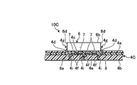
電子部品6としては、例えば、BGA(ball grid array)、CSP(chip size package)、QFN(quad flat non-leaded package)、LGA(land grid array)、フリップチップ等の表面実装型の部品が用いられる。このような電子部品6は、図2に示されるように、一例としては、面6aと、この面6aの反対側に位置されて面6aと並行した(平行な)面6bと、面6aと面6bとの間に亘って面6aおよび面6bと交叉する方向(本実施形態では一例として直交する方向)に延びた面6dと、を有し、扁平な略直方体状の外観を呈している。また、図示されないが、電子部品6は、一例として、平面視(面6aまたは面6bの法線方向、図2の上方また下方からの視線)では、矩形状(例えば、長方形状や正方形状)の外観を呈することができる。また、面6aには、一つ以上の電極(パッド)6cが設けられている。
As the
図2は、電子部品6に、回路基板4に実装される前の処理(前処理)が施された状態を表している。すなわち、本実施形態では、回路基板4に実装される前に、電子部品6の電極6cには、はんだボール(導電性バンプ)7が載せられるとともに、面6a上に、はんだボール7を取り囲むように封止剤(封止材)8が塗布される。本実施形態では、面6aが第二面の一例であり、面6dが外周面の一例であり、電極6cが第二導体部(導電部)の一例である。また、はんだボール7は接合部の一例であり、封止剤8は封止部の一例である。
FIG. 2 shows a state in which the
封止剤8の主成分は、一例としては、絶縁性かつ熱可塑性を有した合成樹脂材料である。本実施形態では、封止剤8は、好適には、加熱する前の温度(一例としては常温)では固化しており、外面(側面や底面等)を形成している。この場合、回路基板4の所定位置に載置しやすい等、取り扱いやすいという利点がある。
The main component of the
図3に示されるように、本実施形態では、図2に例示された前処理が施された電子部品6が回路基板4上にセットされ(ステップS10、電子部品6の載置ステップ、第一のステップ)、リフロー炉に搬入される等して加熱されてはんだボール7および封止剤8が溶融され(ステップS11、加熱ステップ、第二のステップ)、その後、冷却されてはんだボール7および封止剤8が固化される(ステップS13、冷却ステップ、第三のステップ)。また、ステップS11の実施中あるいはステップS11の実施直後等に、電子部品6と回路基板4とを相互に近付く方向に加重(押圧)してもよい(ステップS12、押圧ステップ、第四のステップ)。
As shown in FIG. 3, in the present embodiment, the
回路基板4は、図4に示されるように、面4aと、この面4aの反対側に位置されて面4aと並行した(平行な)面4bと、を有する。また、本実施形態では、回路基板4には、一例として、電子部品6を収容可能な凹部4cが設けられている。凹部4cは、面4a側に開口し、平面視(面4aの法線に沿った方向、図4の上方からの視線)では矩形状(例えば、長方形状や正方形状)に設けられている。凹部4cの底部である底面4eには、電極4fが設けられている。電極4fは、所定の位置に設けられた電子部品6の電極6cと対向する。また、凹部4cの内周面としての側面4dと、凹部4c内に収容された(位置された)電子部品6の外周面としての面6dとの間には、隙間4gが設けられる。すなわち、凹部4cの平面視での大きさは、電子部品6の平面視での大きさより、隙間4gの分だけ大きい。底面4eは、第一面の一例である。また、電極4fは、第一導体部(導電部)の一例である。なお、回路基板4は、一例として、多層基板として構成されるが、これには限定されない。
As shown in FIG. 4, the
また、封止剤8は、本実施形態では、はんだボール7や、電子部品6の電極6c(一例としては銅)、回路基板4の電極4f(一例としては銅、図4参照)等の金属材料の表面に形成された酸化膜(金属酸化物)を還元する機能を有した添加物を含有している。このような添加物の一例としては、カルボン酸や、ハロゲン化合物等がある。カルボン酸の場合、カルボン酸は酸化膜(金属酸化物)と反応してカルボン酸塩と水が生成され、この反応で酸化膜が除去される。なお、カルボン酸塩は、はんだ等の導体と反応して合金化する。なお、ロジンもカルボン酸と同等に機能する。また、ハロゲン化合物(ハロゲン化アルキル)の場合、加熱によりアルキル基とハロゲン水素化物に分解され、このハロゲン水素化物と酸化膜が反応してハロゲン化金属と水が生成され、この反応で酸化膜が除去される。このような添加物を含有することにより、電極6cとはんだボール7との導通、および電極4fとはんだボール7との導通をより向上しやすくなる。
Further, in the present embodiment, the
しかし、かかる添加物を含有した封止剤8は、加熱の過程(加熱された状態)では変形しやすいため、図2等に示されたようなはんだボール7および封止剤8付きの電子部品6を回路基板4上にただ単に載置しただけでは、電子部品6の所定位置からのずれや、所定姿勢からの傾き等が生じる虞があった。
However, since the
そこで、本実施形態では、回路基板4、電子部品6、および他の部品(後述)のうち少なくとも一つに、回路基板4と電子部品6とを位置決めする位置決め部(案内する案内部、ガイド部)が設けられている。本実施形態では、一例として、凹部4cが位置決め部を含んでいる。具体的には、図4に示されるステップS11で加熱される前のセット状態から、凹部4cの側面4dと電子部品6の面6dとが対向している。よって、電子部品6に慣性力等が作用するなどして、電子部品6が回路基板4の面4a,4b,4e等に沿う方向に移動しようとしても、凹部4cの側面4dと電子部品6の面6dとが相互に接触することにより、電子部品6の移動が抑制される。
Therefore, in the present embodiment, a positioning unit (guide unit for guiding, guide unit) for positioning the
また、図5に示されるように、ステップS11での加熱によるはんだボール7および封止剤8の溶融により、電子部品6は重力等によって回路基板4の凹部4c内に進入する(下降する)。これにより、はんだボール7は回路基板4の厚さ方向(図5の上下方向)に潰されて、回路基板4の電極4fおよび電子部品6の電極6cとの接触面積が増大する。この場合、凹部4c内で封止剤8が存在可能な領域(凹部4c内の電子部品6の面6aと回路基板4の底面4eとの間の領域)の容積が減少する。しかし、本実施形態では、この領域の容積の減少に伴い、溶融した状態の封止剤8は、隙間4gに進入し、この隙間4gを介して当該領域外へ排出されうる。なお、この場合、封止剤8は、ステップS13での冷却後も、この隙間4g内に残存する。よって、隙間4gに封止剤8が残存していることは、隙間4gが当該領域からの封止剤8の流出部分となったことの証拠の一つとなりうる。
Further, as shown in FIG. 5, the
また、封止剤8が溶融した状態で隙間4g内に進入することで、電子部品6は凹部4cの中央に位置決めされやすくなる。さらに、この隙間4gの大きさを、封止剤8の粘度等に応じて適宜に設定することで、この隙間4gにおける毛細管現象を利用して、封止剤8をより排出しやすくすることができる。
Further, the
以上説明したように、本実施形態では、封止剤8に酸化膜を還元する還元剤が含まれた。よって、一例としては、電極4f、はんだボール7、および電極6cの酸化膜を減らしてこれらの接触部分における通電抵抗を減らすことができる。また、本実施形態では、回路基板4に、位置決め部(ガイド部)の少なくとも一部を構成する凹部4cが設けられた。よって、一例としては、電子部品6の回路基板4に対するずれや傾きを抑制しやすくなる。
As described above, in this embodiment, the sealing
また、本実施形態では、電子部品6の外周面の一例である面6dと凹部4cの内周面の一例である側面4dとの間に、隙間4gが設けられた。よって、一例としては、封止剤8をより流動しやすくすることができ、一例としては、封止剤8が流出しにくいことによって不都合(一例としては、電子部品6の傾きや浮き、はんだボール7の潰れ不足等)が生じるのを抑制することができる。また、一例としては、電子部品6の周囲を取り囲む隙間4g、あるいは電子部品6の両側に配置された隙間4gにより、電子部品6を凹部4cの中央に位置させやすくなる。
In the present embodiment, the
<第2実施形態>
本実施形態にかかる基板アセンブリ10A(図7)は、第1実施形態にかかる基板アセンブリ10に替えて用いることができる。また、図3に示された製造方法で製造することができる。本実施形態では、図6に示されるように、凹部4cの深さが、上記第1実施形態の凹部4cに比べて浅い。すなわち、図6,7の状態で、面6aが凹部4cの外に位置されている。よって、図6に示されるように、はんだボール7および封止剤8付きの電子部品6を回路基板4A上に載置した場合、電子部品6と回路基板4Aの凹部4cとの間では位置決め部(ガイド部)は構成されない。しかし、本実施形態では、ステップS11で加熱される前に常温で固化されている封止剤8の側面8aと凹部4cの側面4dとが対向するため、本実施形態でも、凹部4cが位置決め部の少なくとも一部として機能することができる。よって、本実施形態でも、一例としては、電子部品6の回転基板4Aに対するずれや傾きを抑制しやすくなる。また、一例としては、凹部4cによって封止剤8は所定の領域に留まりやすくなるため、これにより、一例としては、電子部品6の位置ずれが抑制されやすくなる。
Second Embodiment
The
さらに、本実施形態では、図7に示されるように、電子部品6の外周部に、溶融して凹部4cから流出した封止剤8によりフィレット8bが形成される。よって、一例としては、電子部品6と回路基板4Aとの接続剛性および接続強度がより高くなりやすい。
Furthermore, in this embodiment, as shown in FIG. 7, a
<第3実施形態>
本実施形態にかかる基板アセンブリ10B(図8)は、第1実施形態にかかる基板アセンブリ10に替えて用いることができる。また、図3に示された製造方法で製造することができる。本実施形態では、回路基板4Bに設けられた凹部4cに、底面4eに開口した凹部4hが設けられている。凹部4hは、凹部4cの外周に沿って環状に形成されることができるし、複数の凹部4hが設けられることもできる。この凹部4hは、封止剤8の流出部分となりうる。よって、本実施形態でも、一例としては、封止剤8をより流動しやすくすることができ、一例としては、封止剤8が流出しにくいことによって不都合(一例としては、電子部品6の傾きや浮き、はんだボール7の潰れ不足等)が生じるのを抑制しやすくなる。凹部4hは、第二凹部の一例である。
<Third Embodiment>
The
<第4実施形態>
本実施形態にかかる基板アセンブリ10C(図9)は、第1実施形態にかかる基板アセンブリ10に替えて用いることができる。また、図3に示された製造方法で製造することができる。本実施形態では、回路基板4Cに設けられた凹部4cに、底面4eに開口して、底面4eと面4bとの間で回路基板4Cを貫通する貫通孔4iが設けられている。貫通孔4iは、封止剤8の流出部分となりうる。よって、本実施形態でも、一例としては、封止剤8をより流動しやすくすることができ、一例としては、封止剤8が流出しにくいことによって不都合(一例としては、電子部品6の傾きや浮き、はんだボール7の潰れ不足等)が生じるのを抑制することができる。貫通孔4iは、貫通部、または第二凹部の一例である。
<Fourth embodiment>
The
<第5実施形態>
本実施形態にかかる基板アセンブリ10D(図11)は、第1実施形態にかかる基板アセンブリ10に替えて用いることができる。また、図3に示された製造方法で製造することができる。本実施形態でも、図10に示されるように、ステップS11で加熱する前のはんだボール7および封止剤8付きの電子部品6は、回路基板4Dに設けられた凹部4c内に収容される。ただし、本実施形態では、図10,11に示されるように、電子部品6の上におもり9が載せられている。このおもり9は、ステップS11で加熱されて封止剤8およびはんだボール7が柔らかくなった際に、電子部品6を、その(おもり9の)重力によって、回路基板4D側に加重(押圧)する。ここで、おもり9の面9aは、回路基板4Dの面9aに当接する。よって、本実施形態によれば、一例としては、封止剤8をより流動しやすくすることができ、一例としては、封止剤8が流出しにくいことによって不都合(一例としては、電子部品6の傾きや浮き、はんだボール7の潰れ不足等)が生じるのを抑制することができる。また、おもり9により、一例としては、はんだボール7をより確実に潰すことができ、一例としては、電極4f、はんだボール7、および電極6cの接触部分における通電抵抗をより一層減らすことができる。おもり9は、押圧部材、加重部材、補助部材、部材の一例である。なお、おもり9は、撤去してもよいし、おもり9を電子部品6上にそのまま残して放熱部材として用いてもよい。
<Fifth Embodiment>
The
<第6実施形態>
本実施形態にかかる基板アセンブリ10E(図12)は、第1実施形態にかかる基板アセンブリ10に替えて用いることができる。また、図3に示された製造方法で製造することができる。本実施形態でも、図12に示されるように、ステップS11で加熱する前のはんだボール7および封止剤8付きの電子部品6は、回路基板4Eに設けられた凹部4c内に収容される。そして、上記第5実施形態と同様に、おもり9が用いられる。ただし、本実施形態では、回路基板4E上のおもり9に対向した位置に、スペーサ11が位置されている。すなわち、スペーサ11は、回路基板4Eとおもり9との間に介在する。本実施形態でも、上記第5実施形態と同様の効果を得ることができる。さらに、本実施形態では、スペーサ11により、一例としては、はんだボール7の形状をより適切に設定しやすくなる。スペーサ11は、治具、部品、部材の一例である。
<Sixth Embodiment>
The
<第7実施形態>
本実施形態にかかる基板アセンブリ10F(ただし、加熱および冷却前の状態、図13)は、第1実施形態にかかる基板アセンブリ10に替えて用いることができる。また、図3に示された製造方法で製造することができる。本実施形態では、回路基板4Fの面4a上に、位置決め部(ガイド部)として、突起(突出部)4jが設けられている。この突起4jが、電子部品6の面6dまたは封止剤8の側面をガイドする。よって、本実施形態によっても、一例としては、電子部品6の回路基板4に対するずれや傾きを抑制しやすくなる。
<Seventh embodiment>
The
<第8実施形態>
本実施形態にかかる基板センブリ10G(図14)は、第1実施形態にかかる基板アセンブリ10に替えて用いることができる。また、図3に示された製造方法で製造することができる。本実施形態では、回路基板4Gの面4a上に、位置決め部として、六角柱状のスタッド12が設けられている。さらに、本実施形態では、電子部品6Gの角部6eに、切欠(凹部)6fが設けられている。この切欠6fには、スタッド12の角部12aが嵌合される(挿入される、対応する)。すなわち、本実施形態では、電子部品6Gに、位置決め部としての凹部が設けられている。本実施形態によっても、一例としては、電子部品6の回路基板4に対するずれや傾きを抑制しやすくなる。スタッド12は、突出部の一例である。
<Eighth Embodiment>
The
<第9実施形態>
また、上述した基板アセンブリ10,10A〜10Gは、図15に示されるような電子機器100に設けることができる。電子機器100は、所謂ノート型のパーソナルコンピュータとして構成されており、矩形状の扁平な第一の本体部102と、矩形状の扁平な第二の本体部103と、を備えている。これら第一の本体部102および第二の本体部103は、ヒンジ部104を介して、例えば回動軸Ax回りに、図15に示される展開状態と図示されない折り畳み状態との間で相対回動可能に、接続されている。
<Ninth Embodiment>
Further, the above-described
第一の本体部102には、筐体(第一筐体)102aの外面としての表面102b側に露出する状態で、入力受付部としてのキーボード105や、ポインティングデバイス107、クリックボタン108等が設けられている。一方、第二の本体部103には、筐体(第二筐体)103aの外面としての表面103bに設けられた開口部103cから露出する状態で、部品としてのLCD(Liquid Crystal Display)等の表示装置としてのディスプレイ106が設けられている。図15に示されるような展開状態では、キーボード105や、ディスプレイ106、ポインティングデバイス107、クリックボタン108等が露出して、ユーザが使用可能な状態となる。一方、折り畳み状態(図示されず)では、表面102b,103b同士が相互に近接した状態で対向して、キーボード105や、ディスプレイ106、ポインティングデバイス107、クリックボタン108等が、筐体102a,103aによって隠された状態となる。
The first
また、第一の本体部102の筐体102aの内部には、回路基板4に、電子部品6や、CPU(central processing unit)、ROM(read only memory)、RAM(random access memory)、その他の部品が実装された基板アセンブリ10や、ハードディスク、冷却ファン等の部品(いずれも図示されず)が収容されている。本実施形態の電子機器100でも、基板アセンブリ10(あるいは基板アセンブリ10A〜10G)を有することにより上記実施形態によって得られる効果と同様の効果が得られる。
Further, inside the
また、第一の本体部102の筐体102a内に、上記第1実施形態で例示した磁気ディスク装置1(図15には図示されず)を収容することができる。その場合、具体的には、例えば、筐体102aの裏面(図示されず)に、磁気ディスク装置1の収容部(図示されず)としての凹部が設けられ、その凹部に磁気ディスク装置1が収容され、磁気ディスク装置1とこの磁気ディスク装置1の回路基板4とがコネクタ(図示されず)を介して電気的に接続される。また、筐体102aの裏面には、磁気ディスク装置1が収容された状態で凹部を覆う蓋(図示されず)が取り付けられる。
The magnetic disk device 1 (not shown in FIG. 15) exemplified in the first embodiment can be accommodated in the
また、磁気ディスク装置1の筐体2を除く内部構成が、電子機器100の筐体102a内に収容された構成とすることもできる。その場合、電子機器100の筐体102aが、磁気ディスク装置1の筐体も兼ねることになる。なお、磁気ディスク装置1は、第二の本体部103の筐体103a内に設けることができるし、複数の磁気ディスク装置1を、電子機器100の筐体102a(または筐体103a)の内部に、設けることもできる。
Further, the internal configuration excluding the
以上、本発明の好適な実施形態について説明したが、本発明は上記実施形態には限定されず、種々の変形が可能である。例えば、各実施形態や実施例の構成を部分的に組み合わせて構成することができる。また、電子機器、記憶装置、磁気ディスク装置、筐体、基板アセンブリ、回路基板、第一面、第一導体部、電子部品、第二面、第二導体部、接合部、封止部、位置決め部、凹部、第二凹部、貫通部、突出部等のスペック(構造や、方向、形状、大きさ、長さ、幅、厚さ、高さ、数、配置、位置、材質等)、ならびに各ステップの方法は、適宜に変更して実施することができる。 The preferred embodiments of the present invention have been described above. However, the present invention is not limited to the above embodiments, and various modifications can be made. For example, the configurations of the embodiments and examples can be partially combined. Also, electronic devices, storage devices, magnetic disk devices, housings, board assemblies, circuit boards, first surfaces, first conductor parts, electronic components, second surfaces, second conductor parts, joints, sealing parts, positioning Specs (structure, direction, shape, size, length, width, thickness, height, number, arrangement, position, material, etc.), etc. The method of steps can be implemented with appropriate changes.
本発明の実施形態によれば、一例としては、電子部品を回路基板により精度良く実装することが可能な電子機器、部品、および基板アセンブリの製造方法を得ることができる。 According to the embodiment of the present invention, as an example, it is possible to obtain an electronic device, a component, and a method for manufacturing a substrate assembly that can mount an electronic component on a circuit board with high accuracy.
1…磁気ディスク装置(電子機器)、2…筐体、4,4A〜4G…回路基板、4c…凹部(位置決め部)、4d…側面(内周面)、4e…底面(第一面)、4g…隙間、4h…凹部(第二凹部)、4i…貫通孔(第二凹部、貫通部)、4j…突出部、6,6G…電子部品、6a…面(第二面)、6d…面(外周面)、7…はんだボール(接合部)、8…封止剤(封止部)、10,10A〜10G…基板アセンブリ、12…スタッド(突出部、位置決め部)、100…電子機器、102a,103a…筐体。 DESCRIPTION OF SYMBOLS 1 ... Magnetic disk apparatus (electronic device), 2 ... Housing | casing, 4,4A-4G ... Circuit board, 4c ... Recessed part (positioning part), 4d ... Side surface (inner peripheral surface), 4e ... Bottom surface (1st surface), 4g ... gap, 4h ... recess (second recess), 4i ... through hole (second recess, penetration), 4j ... projection, 6,6G ... electronic component, 6a ... surface (second surface), 6d ... surface (Outer peripheral surface), 7 ... solder ball (joining part), 8 ... sealant (sealing part), 10, 10A to 10G ... substrate assembly, 12 ... stud (protruding part, positioning part), 100 ... electronic device, 102a, 103a ... casing.
Claims (9)
前記筐体に設けられ、第一面と、この第一面に設けられた第一導体部と、を有した回路基板と、
前記回路基板の前記第一面上に位置され、前記第一面と対向した第二面と、この第二面に設けられた第二導体部と、を有した電子部品と、
前記第一導体部と前記第二導体部との間に介在し、前記第一導体部と前記第二導体部とを電気的に接続した接合部と、
前記第二面に塗布され固化された状態で前記第一面に載せられた後に軟化されさらに固化されることで、前記第一面と前記第二面との間に介在され、前記接合部を封止した、酸化膜を還元する還元剤を含む封止部と、
前記第一面の前記電子部品が設けられる位置と隣接した位置で前記第一面から突出し、その突出側の端部が前記第一面と前記第二面との間に位置され、前記第二面に前記封止部が塗布された前記電子部品が前記第一面に載せられる際に当該第一面に沿って移動しようとした場合にあっても固化された状態の前記封止部と接触することにより前記電子部品が前記第一導体部と前記第二導体部とが対向した位置から外れるのを抑制する位置決め部と、
を備えた、電子機器。 A housing,
A circuit board provided on the housing and having a first surface and a first conductor portion provided on the first surface;
An electronic component having a second surface located on the first surface of the circuit board and facing the first surface, and a second conductor portion provided on the second surface;
A joint portion interposed between the first conductor portion and the second conductor portion, and electrically connecting the first conductor portion and the second conductor portion;
After being applied to the second surface and solidified, after being placed on the first surface, it is softened and further solidified, so that it is interposed between the first surface and the second surface, A sealed portion containing a reducing agent that reduces the oxide film sealed;
The first surface protrudes from the first surface at a position adjacent to the position where the electronic component is provided, and an end on the protruding side is positioned between the first surface and the second surface, and the second surface When the electronic component having the sealing portion applied to the surface is placed on the first surface, the electronic component contacts the sealing portion in a solidified state even when trying to move along the first surface. A positioning part that suppresses the electronic component from coming off from a position where the first conductor part and the second conductor part are opposed to each other ;
With electronic equipment.
前記第一面は前記凹部の底部に位置され、
前記位置決め部は、前記凹部の少なくとも一部を含む、請求項1に記載の電子機器。 The circuit board is provided with a recess,
The first surface is located at the bottom of the recess;
The electronic device according to claim 1, wherein the positioning portion includes at least a part of the concave portion.
前記第一のステップで前記電子部品が載置された前記回路基板が加熱される第二のステップと、
前記第二のステップで加熱された前記電子部品が載置された回路基板が冷却される第三のステップと、
を有し、
前記第一のステップでは、前記電子部品が前記第一面に載せられる際に当該第一面に沿って移動しようとした場合にあっても、前記位置決め部が前記固化された状態の封止剤と接触することにより、前記電子部品が前記導体部と当該導体部に対応する前記第一面に設けられた導体部とが対向した位置から外れるのが抑制される、基板アセンブリの製造方法。 A conductor portion provided on the second surface facing the first surface of the circuit board, the joint portion being joined to the conductor portion, and a seal containing a reducing agent for reducing an oxide film around the joint portion; The electronic component to which the stopper is applied protrudes from the first surface of the circuit board and has an end on the protruding side in the posture in which the joining portion is positioned on the circuit board side on the circuit board. A first step in which the sealing agent in a state solidified by a positioning portion located between one surface and the second surface is placed while being positioned; and
A second step in which the circuit board on which the electronic component is placed in the first step is heated;
A third step in which the circuit board on which the electronic component heated in the second step is placed is cooled;
Have,
In the first step, even when the electronic component is placed on the first surface and is about to move along the first surface, the sealing agent in which the positioning portion is in the solidified state The method of manufacturing a board assembly , wherein the electronic component is prevented from coming out of a position where the conductor part and the conductor part provided on the first surface corresponding to the conductor part are opposed to each other by contacting with the conductor part .
Priority Applications (3)
| Application Number | Priority Date | Filing Date | Title |
|---|---|---|---|
| JP2011080673A JP5127946B2 (en) | 2011-03-31 | 2011-03-31 | Electronic device, electronic component, and method for manufacturing substrate assembly |
| US13/300,379 US20120250275A1 (en) | 2011-03-31 | 2011-11-18 | Electronic device, electronic component, and method of manufacturing circuit board assembly |
| US14/165,363 US20140140022A1 (en) | 2011-03-31 | 2014-01-27 | Electronic device, electronic component, and method of manufacturing circuit board assembly |
Applications Claiming Priority (1)
| Application Number | Priority Date | Filing Date | Title |
|---|---|---|---|
| JP2011080673A JP5127946B2 (en) | 2011-03-31 | 2011-03-31 | Electronic device, electronic component, and method for manufacturing substrate assembly |
Related Child Applications (1)
| Application Number | Title | Priority Date | Filing Date |
|---|---|---|---|
| JP2012235984A Division JP2013051432A (en) | 2012-10-25 | 2012-10-25 | Electronic apparatus, electronic component, and manufacturing method of substrate assembly |
Publications (2)
| Publication Number | Publication Date |
|---|---|
| JP2012216671A JP2012216671A (en) | 2012-11-08 |
| JP5127946B2 true JP5127946B2 (en) | 2013-01-23 |
Family
ID=46927016
Family Applications (1)
| Application Number | Title | Priority Date | Filing Date |
|---|---|---|---|
| JP2011080673A Expired - Fee Related JP5127946B2 (en) | 2011-03-31 | 2011-03-31 | Electronic device, electronic component, and method for manufacturing substrate assembly |
Country Status (2)
| Country | Link |
|---|---|
| US (2) | US20120250275A1 (en) |
| JP (1) | JP5127946B2 (en) |
Families Citing this family (4)
| Publication number | Priority date | Publication date | Assignee | Title |
|---|---|---|---|---|
| USD637192S1 (en) * | 2010-10-18 | 2011-05-03 | Apple Inc. | Electronic device |
| CN103594380B (en) * | 2013-10-24 | 2016-01-27 | 天水华天科技股份有限公司 | Tape welding spherical array flat-four-side pin-less packaging part preparation method |
| CN103730442B (en) * | 2013-12-31 | 2016-06-08 | 天水华天科技股份有限公司 | Band weldering spherical array four limit is without pin package body stack package and preparation method |
| JP2017092092A (en) * | 2015-11-04 | 2017-05-25 | 豊田合成株式会社 | Method of manufacturing light-emitting device |
Family Cites Families (15)
| Publication number | Priority date | Publication date | Assignee | Title |
|---|---|---|---|---|
| JPH02105548A (en) * | 1988-10-14 | 1990-04-18 | Nec Corp | Circuit board for mounting flip chip |
| JPH08203956A (en) * | 1995-01-24 | 1996-08-09 | Murata Mfg Co Ltd | Electronic component and manufacture |
| US5778523A (en) * | 1996-11-08 | 1998-07-14 | W. L. Gore & Associates, Inc. | Method for controlling warp of electronic assemblies by use of package stiffener |
| JP3653460B2 (en) * | 2000-10-26 | 2005-05-25 | 三洋電機株式会社 | Semiconductor module and manufacturing method thereof |
| JP4465891B2 (en) * | 2001-02-07 | 2010-05-26 | パナソニック株式会社 | Semiconductor device |
| JP3865606B2 (en) * | 2001-09-28 | 2007-01-10 | 株式会社ルネサステクノロジ | Manufacturing method of semiconductor device |
| TWI228809B (en) * | 2003-08-07 | 2005-03-01 | Advanced Semiconductor Eng | Flip chip package structure and substrate structure thereof |
| KR101237172B1 (en) * | 2003-11-10 | 2013-02-25 | 스태츠 칩팩, 엘티디. | Bump-on-lead flip chip interconnection |
| US7381904B1 (en) * | 2003-11-26 | 2008-06-03 | Western Digital Technologies, Inc. | Disk drive printed circuit board with component-dedicated alignment line indicators including inner and outer line segments |
| WO2006114957A1 (en) * | 2005-04-18 | 2006-11-02 | Murata Manufacturing Co., Ltd. | Electronic component module |
| JP2006351810A (en) * | 2005-06-15 | 2006-12-28 | Epson Toyocom Corp | Ic (integrated circuit) chip storing container and piezo-oscillator |
| JP4940768B2 (en) * | 2006-06-07 | 2012-05-30 | 住友ベークライト株式会社 | Liquid resin composition and method for manufacturing semiconductor device |
| JP4802987B2 (en) * | 2006-11-08 | 2011-10-26 | 住友ベークライト株式会社 | Adhesive film |
| JP2008300500A (en) * | 2007-05-30 | 2008-12-11 | Panasonic Corp | Semiconductor device, and manufacturing method thereof |
| JP2009260219A (en) * | 2008-03-24 | 2009-11-05 | Hitachi Chem Co Ltd | Method of dicing semiconductor wafer, and method of manufacturing semiconductor device |
-
2011
- 2011-03-31 JP JP2011080673A patent/JP5127946B2/en not_active Expired - Fee Related
- 2011-11-18 US US13/300,379 patent/US20120250275A1/en not_active Abandoned
-
2014
- 2014-01-27 US US14/165,363 patent/US20140140022A1/en not_active Abandoned
Also Published As
| Publication number | Publication date |
|---|---|
| JP2012216671A (en) | 2012-11-08 |
| US20140140022A1 (en) | 2014-05-22 |
| US20120250275A1 (en) | 2012-10-04 |
Similar Documents
| Publication | Publication Date | Title |
|---|---|---|
| JP4691455B2 (en) | Semiconductor device | |
| JP5127946B2 (en) | Electronic device, electronic component, and method for manufacturing substrate assembly | |
| JP2007048976A (en) | Printed circuit board and electronic instrument equipped therewith | |
| JP2013123011A (en) | Electronic apparatus | |
| US20220256709A1 (en) | Electronic component package body, electronic component assembly structure, and electronic device | |
| CN108550558B (en) | Packaging structure and welding method | |
| JP2013051432A (en) | Electronic apparatus, electronic component, and manufacturing method of substrate assembly | |
| JP2007088020A (en) | Circuit structure | |
| WO2010070779A1 (en) | Anisotropic conductive resin, substrate connecting structure and electronic device | |
| JP2012089898A (en) | Solder ball and semiconductor package | |
| JP2008270303A (en) | Multilayer semiconductor device | |
| JP4093156B2 (en) | Semiconductor device manufacturing jig, semiconductor device manufacturing method, and semiconductor device | |
| JP4577686B2 (en) | Semiconductor device and manufacturing method thereof | |
| JP2007258448A (en) | Semiconductor device | |
| JP4324773B2 (en) | Manufacturing method of semiconductor device | |
| JP2002359336A (en) | Semiconductor device | |
| JP4952438B2 (en) | Thermal fuse | |
| JP2016162813A (en) | Printed circuit board and soldering method | |
| JP2011076920A (en) | Electronic component, substrate unit, and information processing device | |
| JP4853276B2 (en) | Manufacturing method of semiconductor device | |
| JP2010010212A (en) | Printed circuit board, electronic instrument and semiconductor package | |
| JP4996729B2 (en) | Electronics and board assembly | |
| JP2006013435A (en) | Internal connection structure and internal connection method for electronic device | |
| JP4998146B2 (en) | Thermal fuse | |
| JP2000286360A (en) | Semiconductor device, manufacture thereof, circuit board, and electronic equipment |
Legal Events
| Date | Code | Title | Description |
|---|---|---|---|
| A521 | Request for written amendment filed |
Free format text: JAPANESE INTERMEDIATE CODE: A523 Effective date: 20120829 |
|
| TRDD | Decision of grant or rejection written | ||
| A01 | Written decision to grant a patent or to grant a registration (utility model) |
Free format text: JAPANESE INTERMEDIATE CODE: A01 Effective date: 20121002 |
|
| A01 | Written decision to grant a patent or to grant a registration (utility model) |
Free format text: JAPANESE INTERMEDIATE CODE: A01 |
|
| A61 | First payment of annual fees (during grant procedure) |
Free format text: JAPANESE INTERMEDIATE CODE: A61 Effective date: 20121030 |
|
| FPAY | Renewal fee payment (event date is renewal date of database) |
Free format text: PAYMENT UNTIL: 20151109 Year of fee payment: 3 |
|
| LAPS | Cancellation because of no payment of annual fees |