JP5122505B2 - Power conversion apparatus and control method thereof - Google Patents
Power conversion apparatus and control method thereof Download PDFInfo
- Publication number
- JP5122505B2 JP5122505B2 JP2009054834A JP2009054834A JP5122505B2 JP 5122505 B2 JP5122505 B2 JP 5122505B2 JP 2009054834 A JP2009054834 A JP 2009054834A JP 2009054834 A JP2009054834 A JP 2009054834A JP 5122505 B2 JP5122505 B2 JP 5122505B2
- Authority
- JP
- Japan
- Prior art keywords
- phase
- voltage
- voltage command
- value
- current
- Prior art date
- Legal status (The legal status is an assumption and is not a legal conclusion. Google has not performed a legal analysis and makes no representation as to the accuracy of the status listed.)
- Active
Links
Images


Classifications
-
- H—ELECTRICITY
- H02—GENERATION; CONVERSION OR DISTRIBUTION OF ELECTRIC POWER
- H02M—APPARATUS FOR CONVERSION BETWEEN AC AND AC, BETWEEN AC AND DC, OR BETWEEN DC AND DC, AND FOR USE WITH MAINS OR SIMILAR POWER SUPPLY SYSTEMS; CONVERSION OF DC OR AC INPUT POWER INTO SURGE OUTPUT POWER; CONTROL OR REGULATION THEREOF
- H02M7/00—Conversion of ac power input into dc power output; Conversion of dc power input into ac power output
- H02M7/42—Conversion of dc power input into ac power output without possibility of reversal
- H02M7/44—Conversion of dc power input into ac power output without possibility of reversal by static converters
- H02M7/48—Conversion of dc power input into ac power output without possibility of reversal by static converters using discharge tubes with control electrode or semiconductor devices with control electrode
- H02M7/53—Conversion of dc power input into ac power output without possibility of reversal by static converters using discharge tubes with control electrode or semiconductor devices with control electrode using devices of a triode or transistor type requiring continuous application of a control signal
- H02M7/537—Conversion of dc power input into ac power output without possibility of reversal by static converters using discharge tubes with control electrode or semiconductor devices with control electrode using devices of a triode or transistor type requiring continuous application of a control signal using semiconductor devices only, e.g. single switched pulse inverters
- H02M7/5387—Conversion of dc power input into ac power output without possibility of reversal by static converters using discharge tubes with control electrode or semiconductor devices with control electrode using devices of a triode or transistor type requiring continuous application of a control signal using semiconductor devices only, e.g. single switched pulse inverters in a bridge configuration
- H02M7/53871—Conversion of dc power input into ac power output without possibility of reversal by static converters using discharge tubes with control electrode or semiconductor devices with control electrode using devices of a triode or transistor type requiring continuous application of a control signal using semiconductor devices only, e.g. single switched pulse inverters in a bridge configuration with automatic control of output voltage or current
-
- H—ELECTRICITY
- H02—GENERATION; CONVERSION OR DISTRIBUTION OF ELECTRIC POWER
- H02M—APPARATUS FOR CONVERSION BETWEEN AC AND AC, BETWEEN AC AND DC, OR BETWEEN DC AND DC, AND FOR USE WITH MAINS OR SIMILAR POWER SUPPLY SYSTEMS; CONVERSION OF DC OR AC INPUT POWER INTO SURGE OUTPUT POWER; CONTROL OR REGULATION THEREOF
- H02M7/00—Conversion of ac power input into dc power output; Conversion of dc power input into ac power output
- H02M7/42—Conversion of dc power input into ac power output without possibility of reversal
- H02M7/44—Conversion of dc power input into ac power output without possibility of reversal by static converters
- H02M7/48—Conversion of dc power input into ac power output without possibility of reversal by static converters using discharge tubes with control electrode or semiconductor devices with control electrode
- H02M7/53—Conversion of dc power input into ac power output without possibility of reversal by static converters using discharge tubes with control electrode or semiconductor devices with control electrode using devices of a triode or transistor type requiring continuous application of a control signal
- H02M7/537—Conversion of dc power input into ac power output without possibility of reversal by static converters using discharge tubes with control electrode or semiconductor devices with control electrode using devices of a triode or transistor type requiring continuous application of a control signal using semiconductor devices only, e.g. single switched pulse inverters
- H02M7/539—Conversion of dc power input into ac power output without possibility of reversal by static converters using discharge tubes with control electrode or semiconductor devices with control electrode using devices of a triode or transistor type requiring continuous application of a control signal using semiconductor devices only, e.g. single switched pulse inverters with automatic control of output wave form or frequency
- H02M7/5395—Conversion of dc power input into ac power output without possibility of reversal by static converters using discharge tubes with control electrode or semiconductor devices with control electrode using devices of a triode or transistor type requiring continuous application of a control signal using semiconductor devices only, e.g. single switched pulse inverters with automatic control of output wave form or frequency by pulse-width modulation
-
- H—ELECTRICITY
- H02—GENERATION; CONVERSION OR DISTRIBUTION OF ELECTRIC POWER
- H02M—APPARATUS FOR CONVERSION BETWEEN AC AND AC, BETWEEN AC AND DC, OR BETWEEN DC AND DC, AND FOR USE WITH MAINS OR SIMILAR POWER SUPPLY SYSTEMS; CONVERSION OF DC OR AC INPUT POWER INTO SURGE OUTPUT POWER; CONTROL OR REGULATION THEREOF
- H02M1/00—Details of apparatus for conversion
- H02M1/0003—Details of control, feedback or regulation circuits
- H02M1/0009—Devices or circuits for detecting current in a converter
-
- H—ELECTRICITY
- H02—GENERATION; CONVERSION OR DISTRIBUTION OF ELECTRIC POWER
- H02M—APPARATUS FOR CONVERSION BETWEEN AC AND AC, BETWEEN AC AND DC, OR BETWEEN DC AND DC, AND FOR USE WITH MAINS OR SIMILAR POWER SUPPLY SYSTEMS; CONVERSION OF DC OR AC INPUT POWER INTO SURGE OUTPUT POWER; CONTROL OR REGULATION THEREOF
- H02M1/00—Details of apparatus for conversion
- H02M1/12—Arrangements for reducing harmonics from ac input or output
-
- H—ELECTRICITY
- H02—GENERATION; CONVERSION OR DISTRIBUTION OF ELECTRIC POWER
- H02M—APPARATUS FOR CONVERSION BETWEEN AC AND AC, BETWEEN AC AND DC, OR BETWEEN DC AND DC, AND FOR USE WITH MAINS OR SIMILAR POWER SUPPLY SYSTEMS; CONVERSION OF DC OR AC INPUT POWER INTO SURGE OUTPUT POWER; CONTROL OR REGULATION THEREOF
- H02M1/00—Details of apparatus for conversion
- H02M1/14—Arrangements for reducing ripples from dc input or output
- H02M1/15—Arrangements for reducing ripples from dc input or output using active elements
Landscapes
- Engineering & Computer Science (AREA)
- Power Engineering (AREA)
- Inverter Devices (AREA)
- Control Of Ac Motors In General (AREA)
Description
本発明は、直流母線電流を検出して相電流情報を得る電力変換装置及びその制御方法に関する。 The present invention relates to a power conversion device that detects DC bus current and obtains phase current information, and a control method thereof.
インバータに代表される電力変換装置では、パルス幅変調(以下、「PWM」と記す)により、直流−交流変換、あるいは交流−直流変換の機能を実現している。インバータは、同期モータや誘導モータ等の交流電動機(以下、「電動機」と記す)の駆動システムなどに用いられる。 In a power converter represented by an inverter, a DC-AC conversion function or an AC-DC conversion function is realized by pulse width modulation (hereinafter referred to as “PWM”). The inverter is used in a drive system of an AC electric motor (hereinafter referred to as “electric motor”) such as a synchronous motor or an induction motor.
電動機を駆動する電力変換装置では、精度の良い制御を実現するために相電流の検出手段が必要となる。近年、たとえば、特許文献1、特許文献2及び特許文献3等において、電流センサなどの外部電流検出手段を用いずに電力変換装置の直流母線電流から電動機に流れる交流電流の情報を取得する方法が提案されている。これらの技術により、専用の電流センサを用いる必要がなくなり、装置の部品点数が減り、省スペース化と製造コストの低減が可能となる。
In a power conversion device that drives an electric motor, a means for detecting a phase current is required to realize accurate control. In recent years, for example, in
まず、後の説明のため、三相電圧指令の瞬間値を大きい順に並べたとき最大となる相を最大相、2番目に大きい相を中間相、3番目に大きい相を最小相と呼称することとする。 First, for the following explanation, when the instantaneous values of the three-phase voltage command are arranged in descending order, the largest phase is called the maximum phase, the second largest phase is the intermediate phase, and the third largest phase is called the minimum phase. And
特許文献2では、相電流情報を取得するために、PWM信号を生成する三角波キャリア信号の1周期を前半と後半に分け、前後半いずれかの期間で相電圧指令値に所定値を加算、あるいは減算し、直流母線にパルス状に流れる相電流の通流時間を一時的に長くする。こうすることで、線間電圧値を広げ、直流母線にパルス状に流れる相電流(以下、これをパルス状電流と呼ぶ)の通流時間を一時的に長くして、相電流情報を取得するのである。
In
ここで、前記の電圧指令に対する補正は、最大相に補正量を加算あるいは最小相に補正量を減算することが最良の実施形態とされてきた。 Here, the correction of the voltage command has been best performed by adding the correction amount to the maximum phase or subtracting the correction amount from the minimum phase.
しかし、一般にPWMパルス生成器において、三角波キャリア信号と比較される各相の電圧指令値には上限値及び下限値が設けられており、補正量を加減算した結果、前記上限値あるいは下限値を超過してしまうことがある。このような場合には、十分に前記パルス状電流の通流時間を確保できず、電流検出が出来ない期間が発生してしまい、電動機制御精度が悪化する問題となる。 However, in general, in the PWM pulse generator, an upper limit value and a lower limit value are provided for the voltage command value of each phase to be compared with the triangular wave carrier signal, and as a result of adding or subtracting the correction amount, the upper limit value or the lower limit value is exceeded. May end up. In such a case, a sufficient period of time for the pulsed current cannot be secured, and a period during which current cannot be detected occurs, resulting in a problem that the motor control accuracy deteriorates.
上記の状況は、例えば電動機が高速で回転している場合のように、補正前の電圧指令値の絶対値が大きく、小さい補正量でも上限値または下限値を超過してしまう場合や、必要となる補正量が大きい場合に発生する。補正量が大きい場合としては、キャリア周波数が高い場合、あるいは、パルス状電流の立ち上がり時に発生し、検出誤差原因となるリンギングノイズの持続時間が長い場合などがある。 The above situation is necessary when the absolute value of the voltage command value before correction is large and the upper limit value or the lower limit value is exceeded even with a small correction amount, such as when the electric motor is rotating at high speed. Occurs when the correction amount becomes large. As a case where the correction amount is large, there are a case where the carrier frequency is high, or a case where the duration of ringing noise which occurs at the rising edge of the pulsed current and causes detection error is long.
近年、電動機の高効率化・小型化・低騒音化の傾向が進み、電圧飽和領域の活用やキャリア周波数の高周波化など、上記の状況はますます発生し易くなっており、大きな問題となっている。 In recent years, the trend toward higher efficiency, smaller size, and lower noise of electric motors has progressed, and the above situation is becoming more and more likely to occur, such as the use of voltage saturation regions and higher carrier frequencies. Yes.
また、特許文献3では、PWMのスイッチングに起因して発生する電流リプルによる検出誤差を抑制するための三相電圧指令の補正方法が提案されているが、やはり電圧の上限及び下限による検出不可能状態についての記述はない。
Further,
本発明の目的は、電圧指令値の上限あるいは下限の制約のために電流検出が不可能となることのない直流母線による相電流の検出を実現し、電動機の安定した高精度運転を可能ならしめる電力変換装置及びその制御方法を提供することにある。 An object of the present invention is to realize phase current detection by a DC bus that does not become impossible to detect current due to restriction of the upper limit or lower limit of the voltage command value, and enable stable high-precision operation of the motor. An object of the present invention is to provide a power converter and a control method thereof.
本発明はその一面において、三相電圧指令と三角波キャリア信号とを比較することで電圧指令をPWMパルスに変換するパルス幅変調手段と、前記PWMパルスに基づきスイッチ素子を駆動し直流電圧と三相交流電圧との間に電力変換する電力変換器と、前記電力変換器の主回路の直流母線に流れるパルス状電流を検出する電流検出手段と、前記三相電圧指令の瞬間値をその大きさの順に並べた場合の最大となる相を最大相、2番目に大きい相を中間相、3番目に大きい相を最小相とするとき、最大相と中間相の線間電圧及び中間相と最小相の線間電圧がそれぞれ所定値以上となるように、前記最大相と最小相の電圧指令を補正する電圧指令補正手段とを備えた電力変換装置において、所定の条件において、前記最大相及び/又は最小相の電圧指令のみならず、前記中間相の電圧指令を補正する電圧指令補正手段を備えたことを特徴とする。 In one aspect of the present invention, pulse width modulation means for converting a voltage command into a PWM pulse by comparing a three-phase voltage command and a triangular wave carrier signal, and driving a switch element based on the PWM pulse to drive a DC voltage and a three-phase A power converter for converting power to and from an AC voltage; current detection means for detecting a pulsed current flowing in a DC bus of the main circuit of the power converter; and an instantaneous value of the three-phase voltage command If the largest phase is the maximum phase, the second largest phase is the intermediate phase, and the third largest phase is the minimum phase, the line voltage between the largest phase and the middle phase and the middle phase and the smallest phase In a power conversion device including a voltage command correction unit that corrects the voltage command of the maximum phase and the minimum phase so that the line voltage becomes equal to or greater than a predetermined value, respectively, the maximum phase and / or the minimum is obtained under a predetermined condition. Phase electricity Not command only, characterized by comprising a voltage command correcting means for correcting the voltage command of the intermediate phase.
本発明の望ましい実施態様においては、前記所定の条件を、前記最大相あるいは最小相の電圧指令値を補正することによって、電圧指令値の上限値又は下限値を逸脱する場合に設定する。 In a preferred embodiment of the present invention, the predetermined condition is set when the voltage command value of the maximum phase or the minimum phase is corrected to deviate from the upper limit value or the lower limit value of the voltage command value.
また、本発明の望ましい実施態様においては、電圧指令補正手段により、三角波キャリア信号周期の半分を単位周期として電圧指令を補正し、単位周期の整数倍の期間における電圧指令の補正量の平均値が、零あるいは略零となるように設定する。 Further, in a preferred embodiment of the present invention, the voltage command correction means corrects the voltage command using a half of the triangular wave carrier signal period as a unit period, and an average value of the correction amount of the voltage command in a period that is an integral multiple of the unit period is obtained. , Set to zero or nearly zero.
さらに、本発明の望ましい実施態様においては、電圧指令補正量の平均を零または略零となる期間を、単位周期の奇数倍に設定するとともに、その中心に当たる単位周期で電流を検出するように設定する。 Further, in a preferred embodiment of the present invention, the period during which the average voltage command correction amount is zero or substantially zero is set to an odd multiple of the unit period, and the current is detected in the unit period corresponding to the center. To do.
本発明の望ましい実施態様によれば、電圧指令値の上限あるいは下限の制約のために電流検出が不可能となることなく直流母線による相電流の検出を実現し、電動機の安定した高精度運転を実現する電力変換装置及びその制御方法を提供することができる。 According to a preferred embodiment of the present invention, it is possible to detect a phase current by a DC bus without making it impossible to detect a current due to an upper limit or a lower limit of a voltage command value, and to realize stable and high-precision operation of an electric motor. A power converter to be realized and a control method thereof can be provided.
本発明の望ましい実施態様によれば、従来方法では直流母線から電流検出が不可能となる高速運転時、三角波キャリア周波数が高い条件、リンギングノイズ持続時間が長い悪環境などの運転条件においても適切に電流検出を実現できる。 According to a preferred embodiment of the present invention, during high speed operation where current detection is impossible from a DC bus with the conventional method, it is suitable even in operating conditions such as a high triangular wave carrier frequency and a bad environment with a long ringing noise duration. Current detection can be realized.
本発明のその他と目的と特徴は、以下に述べる実施形態の中で明らかにする。 Others, objects, and features of the present invention will be clarified in the embodiments described below.
以下、本発明の実施例を図面を参照して詳細に説明する。 Hereinafter, embodiments of the present invention will be described in detail with reference to the drawings.
図1は、本発明の実施例1による電力変換装置の全体構成図である。図1では、マイコン4内部は情報の流れを、それ以外は電気回路(実際の電流の流れ)を表している。
1 is an overall configuration diagram of a power conversion device according to a first embodiment of the present invention. In FIG. 1, the inside of the
本実施例においては、直流電源1と、直流母線に接続された電流検出手段3と、前記電流検出手段3から得られた電流情報を基にPWM信号を出力するマイコン4と、前記PWM信号に従って前記直流電源1の電力を交流電力に変換する電力変換部主回路5と、変換された電力によって仕事を行う交流電動機2を備えている。
In the present embodiment, the
前記マイコン4は、まず、前記電流検出手段3により検出される直流母線電流IDC信号が入力され、三相平衡電流Iuc,Ivc,Iwcを再現して出力する電流検出部7を備えている。次に、三相平衡電流Iuc,Ivc,Iwcと、外部から任意に与えられる電流指令Iu*,Iv*,Iw*(以下、記号添字の「*」は指令値を意味する)とが入力され、第1の三相電圧指令Vu*、Vv*、Vw*を演算して出力する電圧指令演算部8を備える。ここで、電流指令Iu*,Iv*,Iw*の代わりに、これを回転座標系に変換したId*,Iq*で与えることもある。また、第1の三相電圧指令Vu*,Vv*,Vw*から電圧指令補正量ΔVu,ΔVv,ΔVwを演算する電圧指令補正量演算部10と、第1の電圧指令と電圧指令補正量を加算して第2の三相電圧指令Vu**,Vv**,Vw**を演算する電圧指令補正部9とを備えている。さらに、最終的に得られた第2の三相電圧指令Vu**,Vv**,Vw**を、PWMによりスイッチ信号へと変換するPWM変換手段11とを備える。
The
前記電力変換部主回路5は、前記スイッチ信号により直流電源1の電力を交流電力に変換して交流電動機に三相平衡電流Iu,Iv,Iwを流す。この相電流は、電力変換部主回路5のスイッチ状態によっては直流母線を流れるため、直流母線電流にはパルス状に相電流が流れることになる。電流検出部7は、第2の電圧指令値から相電流検出が検出可能かどうかを判定し、検出可能ならば相電流を検出するタイミングを設定して電流検出を行い、検出した電流がどの相に当たるかを判定し、検出したIDCから、Iuc,Ivc,Iwcを再現する。
The power converter main circuit 5 converts the power of the
次に、本実施例の特徴である電圧指令補正部9について述べる。 Next, the voltage command correction unit 9 that is a feature of the present embodiment will be described.
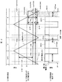
図2は、本発明の実施例1における直流母線電流と三相電圧の関係説明図であり、三角波キャリア信号と直流母線電流波形を模式的に表す。三角波キャリアの一周期は、三角波の単調増加期間および単調減少期間の各半周期からなる。直流母線電流IDCには、三角波キャリアの半周期(以下、これを単位周期と呼ぶ。)につき、2相分の相電流情報がパルス状に現れることが知られている。得られる電流相は、単位周期における電圧最大相と電圧最小相であり、図2に示すように、三角波キャリアの単調増加期間k=1,3と単調減少期間k=2,4でパルスが現れる順番が変わる。図2では、前記電流検出手段3によって各単位周期に検出する2相分の電流値を、検出する順にIDC1,IDC2と表現している。 FIG. 2 is an explanatory diagram of the relationship between the DC bus current and the three-phase voltage in the first embodiment of the present invention, and schematically shows a triangular wave carrier signal and a DC bus current waveform. One period of the triangular wave carrier is composed of half periods of a monotone increasing period and a monotonic decreasing period of the triangular wave. In the DC bus current IDC, it is known that phase current information for two phases appears in a pulse form per half cycle of a triangular wave carrier (hereinafter referred to as a unit cycle). The obtained current phases are the maximum voltage phase and the minimum voltage phase in the unit cycle, and as shown in FIG. 2, pulses appear in the monotonic increase periods k = 1, 3 and the monotone decrease periods k = 2, 4 of the triangular wave carrier. The order changes. In FIG. 2, the current values for two phases detected in each unit cycle by the current detection means 3 are expressed as IDC1 and IDC2 in the order of detection.
直流母線電流から単位周期に得られる相電流情報は、三相交流電流のうち2相分のみであるが、三相交流電流Iu,Iv,Iwは平衡交流であるため、Iu+Iv+Iw=0が常に成り立っている。このため、残り1相分の情報は他の2相から求められる。 The phase current information obtained in a unit cycle from the DC bus current is only for two phases of the three-phase AC current, but since the three-phase AC currents Iu, Iv, and Iw are balanced AC, Iu + Iv + Iw = 0 always holds. ing. For this reason, information for the remaining one phase is obtained from the other two phases.
ここで、各瞬間における三相の電圧指令のうち最大のものを最大相としてV1、最小のものを最小相としてV3、中間のものを中間相としてV2と記号で示し、対応した相電流をそれぞれ、I1,I2,I3と表記する。図2では、大小関係がVu>Vv>Vwとなっているため、V1=Vu,V2=Vv,V3=Vwである。 Here, among the three-phase voltage commands at each moment, the maximum one is indicated as V1 as the maximum phase, the minimum one as V3 as the minimum phase, the intermediate one as V2 as the intermediate phase, and the corresponding phase currents respectively. , I1, I2, and I3. In FIG. 2, since the magnitude relationship is Vu> Vv> Vw, V1 = Vu, V2 = Vv, and V3 = Vw.
各単位周期において、直流母線電流に現れる電圧最大相電流I1及び電圧最小相電流I3の通流時間(以下、電流パルス幅と呼ぶ)は、V1及びV3の中間相電圧V2からの線間電圧値に依存して決まる。すなわち、図2における補正前を表す単位周期k=1,2から明らかなように、例えば、最小相電流パルスの通流時間は、V23*=V2*−V3*で決まり、最大相電流パルスの通流時間はV12*=V*1−V2*により決まる。 In each unit period, the duration of the maximum voltage phase current I1 and the minimum voltage phase current I3 appearing in the DC bus current (hereinafter referred to as current pulse width) is the line voltage value from the intermediate phase voltage V2 of V1 and V3. Depends on. That is, as is clear from the unit periods k = 1 and 2 representing the pre-correction in FIG. 2, for example, the passing time of the minimum phase current pulse is determined by V23 * = V2 * −V3 * , and the maximum phase current pulse The flow time is determined by V12 * = V * 1-V2 * .
パルス状電流から電流検出を行うためには、電流パルス幅が所定値以上であることが必要となる。ここでいう「所定値」とは、半導体素子のアーム短絡を防止するためのデッドタイム期間や、リンギングノイズが発生している期間、あるいは、A/D変換器のサンプルホールド時間などを考慮した最小幅であり、ハード的な制約で決まると考えてよい。この電流検出可能な電流パルス幅の最小値を最小パルス幅Tpwと定義する。 In order to detect current from a pulsed current, the current pulse width needs to be a predetermined value or more. The “predetermined value” here is a maximum time considering a dead time period for preventing an arm short circuit of a semiconductor element, a period during which ringing noise is generated, a sample hold time of an A / D converter, or the like. It can be considered to be narrow and determined by hardware constraints. The minimum current pulse width that can be detected is defined as the minimum pulse width Tpw.
なお、図2では、k=2において、V12は十分大きいがV23が小さいため、IDC1の検出は可能であるが、IDC2の通流時間tが最小パルス幅Tpwより短く(t<Tpw)なり、電流検出が不可能となっている。 In FIG. 2, when k = 2, V12 is sufficiently large but V23 is small, so that IDC1 can be detected, but the IDC2 flow time t is shorter than the minimum pulse width Tpw (t <Tpw), Current detection is impossible.
まとめると、直流母線電流IDCから相電流検出が可能となる条件は、次の(1)式で表される。 In summary, the condition that enables the phase current detection from the DC bus current IDC is expressed by the following equation (1).
V12>=Vpw、かつ、V23>=Vpw…………………………………(1)
ここで、必要線間電圧Vpwは、最小パルス幅Tpwに相当する線間電圧である。電流検出時における電圧指令補正部9の目的は、第1の電圧指令が(1)式を満たさない場合、第2の電圧指令が(1)式を満たすように電圧指令値を補正することにある。
V12> = Vpw and V23> = Vpw ....................................... (1)
Here, the necessary line voltage Vpw is a line voltage corresponding to the minimum pulse width Tpw. The purpose of the voltage command correction unit 9 at the time of current detection is to correct the voltage command value so that the second voltage command satisfies the equation (1) when the first voltage command does not satisfy the equation (1). is there.
次に、本発明の最も特徴的な電圧指令補正量演算の内容について説明する。 Next, the most characteristic content of the voltage command correction amount calculation of the present invention will be described.
図3は、本発明の実施例1における電圧指令補正量演算部の処理フロー図である。所定の周期毎に電流検出時の電圧指令補正量演算プロセス30が呼び出されると、入力された第1の電圧指令Vu*,Vv*,Vw*を大きい順にV1*,V2*,V3*と定義する(処理31)。続いて、(1)式を満たすように、最大相電圧V1*及び最小相電圧V3*を補正したとき、出力電圧上限値Vmaxあるいは電圧下限値Vminを超過しないかどうかチェックを行う。なお、Vmax及びVminは、例えば直流電源1の電圧から決まる電力変換部主回路5の出力可能な最大電圧及び最小電圧で与えられる。
FIG. 3 is a process flow diagram of the voltage command correction amount calculation unit according to the first embodiment of the present invention. When the voltage command correction amount calculation process 30 at the time of current detection is called up at predetermined intervals, the input first voltage commands Vu * , Vv * , Vw * are defined as V1 * , V2 * , V3 * in descending order. (Process 31). Subsequently, when the maximum phase voltage V1 * and the minimum phase voltage V3 * are corrected so as to satisfy the expression (1), it is checked whether the output voltage upper limit value Vmax or the voltage lower limit value Vmin is not exceeded. Note that Vmax and Vmin are given by the maximum voltage and the minimum voltage that can be output from the power converter main circuit 5 determined from the voltage of the
例えば(1)式を満たすように、V1*に補正量ΔV1を加算するとき、(2)式と(3)式を満たすように、ΔV1及びΔV3を決定する。 For example, when the correction amount ΔV1 is added to V1 * so as to satisfy the expression (1), ΔV1 and ΔV3 are determined so as to satisfy the expressions (2) and (3).
V1**−V2*=V1*+ΔV1−V2*>=Vpw………………………(2)
V2**−V3**=V2*−V3*+ΔV3>=Vpw……………………(3)
しかし、このとき出力電圧の最大最小がVmax以上Vmin以下に制限されているとすると、
V1**<Vmax…………………………………………………………………(4)
V3**>Vmin…………………………………………………………………(5)
でなければならない。この条件をまとめると以下のようになる。
V1 ** -V2 * = V1 * + ΔV1-V2 *> = Vpw (2)
V2 ** -V3 ** = V2 * -V3 * + ΔV3> = Vpw (3)
However, at this time, if the maximum and minimum of the output voltage is limited to Vmax or more and Vmin or less,
V1 ** <Vmax ………………………………………………………………… (4)
V3 ** > Vmin ………………………………………………………………… (5)
Must. The conditions are summarized as follows.
V2*+Vpw<Vmax…………………………………………………………(6)
V2*−Vpw>Vmin…………………………………………………………(7)
(6)式を満たしていないとき、第2の電圧指令値V1**がVmaxを超過し、最大相電流を検出することができなくなる。同様に(7)式が満たされない場合、第2の電圧指令値V3**がVminを下回るため、最小相電流を検出することができなくなる。
V2 * + Vpw <Vmax ………………………………………………………… (6)
V2 * −Vpw> Vmin ………………………………………………………… (7)
When the expression (6) is not satisfied, the second voltage command value V1 ** exceeds Vmax, and the maximum phase current cannot be detected. Similarly, when the expression (7) is not satisfied, the second voltage command value V3 ** is lower than Vmin, so that the minimum phase current cannot be detected.
(6)式,(7)式が共に満たされる場合、(2)式,(3)式を満たすΔV1、ΔV3を計算すればよく、通常ΔV1及びΔV3は(2)式および(3)式を満たす最小の値に設定する(処理32)。 When both the expressions (6) and (7) are satisfied, ΔV1 and ΔV3 satisfying the expressions (2) and (3) may be calculated. Usually, ΔV1 and ΔV3 are expressed by the expressions (2) and (3). The minimum value to be satisfied is set (process 32).
(7)式のみが満たされない場合、(3)式を満たすいかなるΔV3でもV3**がVminを下回ってしまうため、V23*がVpw以上確保することが出来ず、最小相電流を検出することが出来なくなる。 If only equation (7) is not satisfied, V3 ** will be less than Vmin at any ΔV3 that satisfies equation (3), so V23 * cannot be secured above Vpw, and the minimum phase current can be detected. It becomes impossible.
そこで、本実施例では、V3**=Vminとし、V23*がVpwに満たない分をV2*に加算してやることでVpwを確保する。このとき、V2*の増加に伴いV12*が小さくなるため、(1)式を満たさなくなる可能性がある。そこでV1*もV2**からVpwを確保できる値になるまで補正する(処理33)。 Therefore, in this embodiment, Vpw is ensured by setting V3 ** = Vmin and adding V23 * to V2 * which is less than Vpw. At this time, since V12 * becomes smaller as V2 * increases, the expression (1) may not be satisfied. Therefore, V1 * is also corrected from V2 ** until it reaches a value that can secure Vpw (process 33).
同様に(6)式のみが満たされない場合、V1**=Vmaxとし、V12*がVpwに満たない分、V2*を減算することで確保する(処理34)。 Similarly, when only the expression (6) is not satisfied, V1 ** = Vmax is set, and V12 * is secured by subtracting V2 * as much as Vpw (process 34).
もし(6)式,(7)式共に満たされない場合は、ΔV1,ΔV2,ΔV3を零として電流検出を諦める(処理35)。 If both the equations (6) and (7) are not satisfied, ΔV1, ΔV2 and ΔV3 are set to zero and the current detection is given up (processing 35).
以上のプロセスで演算されたΔV1及びΔV3が、(8)式,(9)式を満たす場合は、補正しなくても、もともと(数1)を満たしている条件である。 When ΔV1 and ΔV3 calculated in the above process satisfy the expressions (8) and (9), the condition is that the expression (1) is originally satisfied without correction.
ΔV1<0……………………………………………………………………………(8)
ΔV3>0……………………………………………………………………………(9)
このため、ΔV1=0、ΔV3=0としてよい(処理36,37)。
ΔV1 <0 ……………………………………………………………………………… (8)
ΔV3> 0 …………………………………………………………………………… (9)
Therefore, ΔV1 = 0 and ΔV3 = 0 may be set (processes 36 and 37).
処理31の逆の処理を行い、最後に演算したΔV1,ΔV2,ΔV3をΔVu,ΔVv,ΔVwに戻して引数に返して処理を終わる。
The reverse process of the
これらの処理により、第2の三相電圧指令は(1),(4),(5)式を全て満たすため、適切な電流検出を実現し、かつ電圧指令補正量を最小に抑えることが出来る。 With these processes, the second three-phase voltage command satisfies all the expressions (1), (4), and (5), so that appropriate current detection can be realized and the voltage command correction amount can be minimized. .
以上の実施例1の動作の一例を、図2の単位周期k=4に示している。この例では、最小相電圧VW*(V3*)をΔV3で補正すると共に、本発明により、中間相電圧VV*(V2*)に対しても、ΔV2による補正を追加している。この結果、電流IDC2のパルス幅tが、t≧Tpwに延び、電流検出を可能にしている。 An example of the operation of the first embodiment is shown in unit cycle k = 4 in FIG. In this example, the minimum phase voltage VW * (V3 * ) is corrected by ΔV3, and the correction by ΔV2 is added to the intermediate phase voltage VV * (V2 * ) according to the present invention. As a result, the pulse width t of the current IDC2 extends to t ≧ Tpw, enabling current detection.
次に、本実施例の効果について述べる。 Next, the effect of the present embodiment will be described.
特許文献2で提案されているように、従来では(1)式を満たすため、電圧指令補正は最大相電圧V1*または最小相電圧V3*の絶対値が大きくなる方向(中間相電圧V2*から離れる方向)に行うことが最良の実施形態であるとされてきた。これは、V2*を動かすと一方の電流パルス幅は大きくなるが他方の電流パルス幅が小さくなるデメリットがあるためである。
As proposed in
しかし(1)V1*あるいはV3*の絶対値が大きい場合や、(2)最小パルス幅Tpwを確保するために必要な線間電圧Vpwが大きい状況では、電圧上限値Vmax及び下限値Vminまでの余裕が小さくなり、Vpwを確保することができなくなる。 However, (1) when the absolute value of V1 * or V3 * is large, or (2) when the line voltage Vpw necessary for securing the minimum pulse width Tpw is large, the voltage values up to the upper limit value Vmax and the lower limit value Vmin. The margin becomes small and Vpw cannot be secured.
前記(1)V1*あるいはV3*の絶対値が大きい場合とは、例えば交流電動機2の速度が高速になる場合が挙げられる。このとき内部逆起電力が大きくなるため、第1の電圧指令が大きくなる。このように、電動機の高速運転時に、本発明は特に有用である。
The case where the absolute value of (1) V1 * or V3 * is large includes, for example, a case where the speed of the
また、前記(2)Vpwが大きい状況とは、例えばキャリア周波数が高い場合が考えられる。高周波キャリア条件では、同じ最小パルス幅Tpwであっても、最小線間電圧Vpwが大きくなる。これは、図2の三角波キャリアの傾きがキャリア周波数の増大に伴って急峻となることを考えれば自明である。近年の半導体素子の低損失化とユーザーの静音化ニーズの高まりによるキャリア周波数の高周波化傾向に対して、本発明は効果的である。 In addition, the situation (2) where Vpw is large may be, for example, a case where the carrier frequency is high. Under the high frequency carrier condition, the minimum line voltage Vpw increases even if the same minimum pulse width Tpw is used. This is self-evident when considering that the slope of the triangular wave carrier in FIG. 2 becomes steep as the carrier frequency increases. The present invention is effective against the trend toward higher carrier frequencies due to the recent low loss of semiconductor elements and increasing user's need for noise reduction.
その他に、Vpwが大きい状況として、リンギングノイズ環境の悪条件が考えられる。半導体素子のスイッチ動作に伴ってパルス状電流に現れる高周波リンギングノイズは、装置の設置環境に依存して持続時間が変わるため、それに伴いVpwも変化することになる。多様な環境に対する適用性に関して、本発明は効果的である。 In addition, as a situation where Vpw is large, an adverse condition of a ringing noise environment can be considered. The high-frequency ringing noise that appears in the pulsed current accompanying the switching operation of the semiconductor element changes in duration depending on the installation environment of the device, so that Vpw also changes accordingly. The present invention is effective with respect to applicability to various environments.
本実施形態によれば、電圧指令補正部9は、三角波キャリアの半周期を単位周期として電圧指令値の最大相及び最小相に補正量を加算し、その結果、電圧上限や下限値を超過する場合には、その超過分だけ中間相を加算して電流検出に必要な線間電圧を確保する。これにより、電圧上限及び下限のために電流検出が不可能であった条件下でも、高精度な電流検出が可能となる。すなわち、電動機の高速運転時や三角波キャリア周波数の高周波条件、リンギングノイズ悪環境のような多様な環境に対しても高精度な制御が可能となる。 According to the present embodiment, the voltage command correction unit 9 adds the correction amount to the maximum phase and the minimum phase of the voltage command value using the half cycle of the triangular wave carrier as a unit cycle, and as a result, exceeds the voltage upper limit or lower limit value. In this case, the intermediate phase is added by the excess amount to ensure the line voltage necessary for current detection. This enables highly accurate current detection even under conditions where current detection is impossible due to the upper and lower voltage limits. That is, high-precision control is possible even in various environments such as high-speed operation of an electric motor, high-frequency conditions of a triangular wave carrier frequency, and a bad environment of ringing noise.
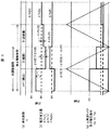
図4は、本発明の実施例2における直流母線電流と三相電圧の関係説明図である。この図を用いて、本実施例2の特徴を説明する。本実施例では、実施例1のように電流検出時に加算された電圧指令補正量を、電流検出を行わない期間において補償を行う。これにより、第2の電圧指令と第1の電圧指令とを同等とし、正常な運転を維持することが出来る。補償の方法については、特許文献2及び特許文献3などで提案されている通り、単位周期のN倍の期間を調整期間として考え、調整期間中の各相の補正量の平均が零または略零となるように電流非検出期間の補正量を設定すればよい。しかし、本発明では中間相も補正しており、補償時に電圧上限あるいは下限を超過する問題が発生する。本実施例ではその対策について述べる。なお、Nは自然数とする。
FIG. 4 is a diagram for explaining the relationship between the DC bus current and the three-phase voltage in the second embodiment of the present invention. Features of the second embodiment will be described with reference to FIG. In the present embodiment, the voltage command correction amount added at the time of current detection as in the first embodiment is compensated during a period in which current detection is not performed. As a result, the second voltage command and the first voltage command can be made equivalent and normal operation can be maintained. As for the compensation method, as proposed in
説明のため調整期間がNであったとき、調整期間内の各単位周期に序数k=1,2,3,・・・Nをつけて考える。このとき、各単位周期の電圧指令補正量をΔV1[k]、ΔV2[k]、ΔV3[k]とする。N個の単位周期のうち少なくとも一つでは電流検出を行うため、この単位周期を検出期間と呼び、残りの単位周期は補償期間と呼ぶ。ここでは検出期間を調整期間中1回とする。V1[k],V2[k],V3[k]の計算方法については実施例1で述べた通りである。この電流検出時の電圧指令補正量を、ここでは、ΔV10,ΔV20,ΔV30とする。また、調整期間における電圧指令補正量の時間平均を零または略零とするために、電圧指令補正量は各相について次の関係を満たす必要がある。 For the sake of explanation, when the adjustment period is N, an ordinal number k = 1, 2, 3,... At this time, the voltage command correction amount for each unit period is set to ΔV1 [k], ΔV2 [k], and ΔV3 [k]. Since current detection is performed in at least one of the N unit cycles, this unit cycle is called a detection period, and the remaining unit cycles are called compensation periods. Here, the detection period is once during the adjustment period. The calculation method of V1 [k], V2 [k], and V3 [k] is as described in the first embodiment. Here, the voltage command correction amounts at the time of current detection are ΔV10, ΔV20, and ΔV30. Further, in order to set the time average of the voltage command correction amount during the adjustment period to zero or substantially zero, the voltage command correction amount needs to satisfy the following relationship for each phase.
Σ_k=1〜NΔV1[k]=0………………………………………………(10)
Σ_k=1〜NΔV2[k]=0………………………………………………(11)
Σ_k=1〜NΔV3[k]=0………………………………………………(12)
例えば、調整周期において検出が1回行われると仮定すると、補償期間の序数の単位周期においては、次式のように設定するものとする。
Σ_k = 1 to NΔV1 [k] = 0 ……………………………………………… (10)
Σ_k = 1 to NΔV2 [k] = 0 ……………………………………………… (11)
Σ_k = 1 to NΔV3 [k] = 0 ……………………………………………… (12)
For example, assuming that the detection is performed once in the adjustment period, the unit period of the ordinal number of the compensation period is set as follows.
ΔV1[k]=−ΔV10/(N−1)………………………………………(13)
ΔV2[k]=−ΔV20/(N−1)………………………………………(14)
ΔV3[k]=−ΔV30/(N−1)………………………………………(15)
式(13)〜(15)ではΔV1[k]、ΔV2[k]、ΔV3[k]を各kについて同値であるとしたが、式(10)〜(12)を満たしていれば値が異なっていてもよい。例えば、検出期間の前の補償期間では補正量を大きく、後では補正量を小さく設定してもよい。
ΔV1 [k] = − ΔV10 / (N−1) (13)
ΔV2 [k] = − ΔV20 / (N−1) (14)
ΔV3 [k] = − ΔV30 / (N−1) (15)
In Expressions (13) to (15), ΔV1 [k], ΔV2 [k], and ΔV3 [k] are assumed to have the same value for each k, but the values are different if Expressions (10) to (12) are satisfied. It may be. For example, the correction amount may be set to be large in the compensation period before the detection period, and the correction amount may be set to be small later.
更に、第2の電圧指令が電圧上限あるいは下限を超過する問題が発生する。これを防ぐためには、(16)〜(18)式に示す条件を全ての序数kについて満たすようにΔV1[k],ΔV2[k],ΔV3[k]を設定する必要がある。 Furthermore, there arises a problem that the second voltage command exceeds the upper or lower voltage limit. In order to prevent this, it is necessary to set ΔV1 [k], ΔV2 [k], and ΔV3 [k] so that the conditions shown in the equations (16) to (18) are satisfied for all the ordinal numbers k.
V1*+ΔV1[k]<Vmax、V1*+ΔV1[k]>Vmin……(16)
V2*+ΔV2[k]<Vmax、V2*+ΔV2[k]>Vmin……(17)
V3*+ΔV3[k]<Vmax、V3*+ΔV3[k]>Vmin……(18)
ただし、検出期間(k=1のとき)については、実施例1で述べたように、電圧指令補正量を決定するため(16)〜(18)式は満たされる。このため、ここで問題となるのは補償期間においてである。そこで、ΔV1[k],ΔV2[k],ΔV3[k]が(16)〜(18)式を満たさない場合、検出不能と判断して電圧指令補正及び電流検出はしないものとする。
V1 * + ΔV1 [k] <Vmax, V1 * + ΔV1 [k]> Vmin (16)
V2 * + ΔV2 [k] <Vmax, V2 * + ΔV2 [k]> Vmin (17)
V3 * + ΔV3 [k] <Vmax, V3 * + ΔV3 [k]> Vmin (18)
However, for the detection period (when k = 1), as described in the first embodiment, the equations (16) to (18) are satisfied in order to determine the voltage command correction amount. For this reason, the problem here is in the compensation period. Therefore, when ΔV1 [k], ΔV2 [k], and ΔV3 [k] do not satisfy the expressions (16) to (18), it is determined that detection is impossible and voltage command correction and current detection are not performed.
具体的な例として、図4に示すように、N=2とした場合を説明する。図4では、V23*(=V2*−V3*)<Vpwである。したがって、(1)式を満たさないため、このままでは相電流が検出できない。また、検出周期はk=1とする。 As a specific example, a case where N = 2 as shown in FIG. 4 will be described. In FIG. 4, V23 * (= V2 * −V3 * ) <Vpw. Therefore, since the equation (1) is not satisfied, the phase current cannot be detected as it is. The detection cycle is k = 1.
単位周期k=1において、実施例1で説明したように、ΔV1[1]=ΔV10,ΔV2[1]=ΔV20,ΔV3[1]=ΔV30とすることで、ΔV23**=Vpwとし、相電流情報を得る(なお、ここではΔV10=0である)。ここでの補正量を保存しておき、続くk=2の単位周期において、電圧指令補正量ΔV2[2],ΔV3[2]を計算する。N=2より、ΔV1[2]=−ΔV10,ΔV2[2]=−ΔV20,ΔV3[2]=−ΔV30である。更に、ΔV1,ΔV2,ΔV3が(16)〜(18)式を満たすかどうかの判定を行う。 In the unit cycle k = 1, as described in the first embodiment, ΔV1 [1] = ΔV10, ΔV2 [1] = ΔV20, ΔV3 [1] = ΔV30, so that ΔV23 ** = Vpw and the phase current Information is obtained (in this case, ΔV10 = 0). The correction amount here is stored, and the voltage command correction amounts ΔV2 [2] and ΔV3 [2] are calculated in the subsequent unit cycle of k = 2. Since N = 2, ΔV1 [2] = − ΔV10, ΔV2 [2] = − ΔV20, ΔV3 [2] = − ΔV30. Further, it is determined whether ΔV1, ΔV2, and ΔV3 satisfy the expressions (16) to (18).
もし(16)〜(18)式のいずれかを満たさない場合には、検出不可能と判断し、補正及び検出を行わないものとする。この処理により、事前に補償不可能な場合を判断し、補償不全による電動機の運転異常を回避することが出来る。 If any of the equations (16) to (18) is not satisfied, it is determined that the detection is impossible, and correction and detection are not performed. By this process, it is possible to determine in advance a case where compensation is not possible, and to avoid an abnormal operation of the motor due to insufficient compensation.
なお、本実施例では、三角波キャリア信号の単調増加期間を検出期間(k=1)としたが、単調減少期間を検出期間としても良い。 In this embodiment, the monotonically increasing period of the triangular wave carrier signal is the detection period (k = 1), but the monotonically decreasing period may be the detection period.
図5は、本発明の実施例3における直流母線電流と三相電圧の関係説明図である。この図を用いて、本実施例3について、実施例2と異なる点について説明する。本実施例3では、(16)〜(18)式を満たさない場合には(16)〜(18)式を満たすまで一時的にNを増加させて検出を実施する。 FIG. 5 is an explanatory diagram of the relationship between the DC bus current and the three-phase voltage in the third embodiment of the present invention. The difference between the third embodiment and the second embodiment will be described with reference to FIG. In the third embodiment, when the expressions (16) to (18) are not satisfied, the detection is performed by temporarily increasing N until the expressions (16) to (18) are satisfied.
図5では、補償量ΔV20が著しく大きく、k=2において、V2+ΔV2[2]がVminを下回ってしまう場合である。このとき、一時的に調整期間を延長し、次の単位周期(k=3)で補償し切れなかった残りの補償量を補償する。もし、N=3でも補償し切れない場合は、更に調整期間を延ばせばよい。このように調整期間を延長することで、実施例2では検出を諦めていた条件でも相電流検出を行うことが可能となる。 In FIG. 5, the compensation amount ΔV20 is remarkably large, and V2 + ΔV2 [2] falls below Vmin at k = 2. At this time, the adjustment period is temporarily extended to compensate for the remaining compensation amount that could not be compensated for in the next unit cycle (k = 3). If even N = 3 cannot be compensated, the adjustment period may be further extended. By extending the adjustment period in this way, it is possible to perform phase current detection even under conditions where the detection has been given up in the second embodiment.
図6は、本発明の実施例4における直流母線電流と三相電圧の関係説明図である。本実施例は、調整期間を決定する単位周期数Nを奇数とし、検出する単位周期を調整期間の中心に配置するところを特徴とする。図6ではN=3の場合を示している。k=2を検出期間とし、k=1及び3のときを補償期間としている。各検出期間における電圧指令補正量演算は実施例1の方法を用い、補償期間における補正量演算は実施例2で述べた方法を用いて次のように設定する。 FIG. 6 is an explanatory diagram of the relationship between the DC bus current and the three-phase voltage in Example 4 of the present invention. This embodiment is characterized in that the number N of unit cycles for determining the adjustment period is an odd number, and the unit cycle to be detected is arranged at the center of the adjustment period. FIG. 6 shows a case where N = 3. The detection period is k = 2, and the compensation period is when k = 1 and 3. The voltage command correction amount calculation in each detection period is set using the method of the first embodiment, and the correction amount calculation in the compensation period is set as follows using the method described in the second embodiment.
ΔV1[1]=ΔV1[3]=−ΔV10/2………………………………(19)
ΔV2[1]=ΔV2[3]=−ΔV20/2………………………………(20)
ΔV3[1]=ΔV3[3]=−ΔV30/2………………………………(21)
また、補償期間において電圧指令がVmaxあるいはVminを超過する場合については実施例2による方法あるいは実施例3による方法を同様に適用できる。
ΔV1 [1] = ΔV1 [3] = − ΔV10 / 2 (19)
ΔV2 [1] = ΔV2 [3] = − ΔV20 / 2 (20)
ΔV3 [1] = ΔV3 [3] = − ΔV30 / 2 (21)
Further, when the voltage command exceeds Vmax or Vmin during the compensation period, the method according to the second embodiment or the method according to the third embodiment can be similarly applied.
このように調整期間を単位周期の奇数倍としたことで、検出周期が三角波キャリアの単調増加期間と単調減少期間に交互に割り当てられるため、PWMに伴う電流リプルによる電流検出誤差の影響を減らすことが可能となり、高精度な検出が実現できるようになる。 Since the adjustment period is set to an odd multiple of the unit period in this manner, the detection period is alternately assigned to the monotonically increasing period and the monotonically decreasing period of the triangular wave carrier, thereby reducing the influence of current detection errors due to current ripple caused by PWM. Thus, highly accurate detection can be realized.
また、その中心に当たる単位周期で検出を行うようにしたことにより、その範囲内での制御量の変動幅を小さく抑えることができ、安定性に優れた制御を実現できる。 In addition, since the detection is performed in the unit cycle corresponding to the center, the fluctuation range of the control amount within the range can be suppressed to be small, and the control with excellent stability can be realized.
次に、本発明の実施例5を説明する。図6に示した実施例4では、式(19)〜(21)のように補償期間での補正量演算を行ったが、本実施例5では、以下のように補正量演算を行う点が異なっている。 Next, a fifth embodiment of the present invention will be described. In the fourth embodiment shown in FIG. 6, the correction amount calculation is performed in the compensation period as in the equations (19) to (21). However, in the fifth embodiment, the correction amount calculation is performed as follows. Is different.
ΔV1[1]=−ΔV10×m…………………………………………………(22)
ΔV1[3]=−ΔV10×(1−m)………………………………………(23)
ΔV2[1]=−ΔV20×m…………………………………………………(24)
ΔV2[3]=−ΔV20×(1−m)………………………………………(25)
ΔV3[1]=−ΔV30×m…………………………………………………(26)
ΔV3[3]=−ΔV30×(1−m)………………………………………(27)
ここで、mは0<m<1を満たす正の実数である。m=0.5とすれば、実施例4に一致する。本実施例5では、mを0.5より大きい値(例えば0.75)などの値とする。
ΔV1 [1] = − ΔV10 × m ……………………………………………… (22)
ΔV1 [3] = − ΔV10 × (1−m) (23)
ΔV2 [1] = − ΔV20 × m ………………………………………………… (24)
ΔV2 [3] = − ΔV20 × (1−m) (25)
ΔV3 [1] = − ΔV30 × m ……………………………………………… (26)
ΔV3 [3] = − ΔV30 × (1−m) (27)
Here, m is a positive real number that satisfies 0 <m <1. If m = 0.5, it corresponds to the fourth embodiment. In the fifth embodiment, m is a value such as a value larger than 0.5 (for example, 0.75).
図7は、本実施例5の効果を実施例4と比較して模式的に示したもので、電圧最大相を補正したことによって生じる最大相電流I1の高調波成分を表している。実施例4の場合、補償量は検出周期に対して対称をなしているため、その結果現れる高調波成分も対称形をなす。電流検出タイミングは検出周期の末期となるため、結果として高調波成分のピークで検出することとなり、誤差が発生する。それに対して本実施例5では、k=1での補償量を大きめに取ることで検出点のピークの値を小さく抑えることが出来る。これによって、電流検出誤差を小さくすることが出来る。 FIG. 7 schematically shows the effect of the fifth embodiment in comparison with the fourth embodiment, and represents a harmonic component of the maximum phase current I1 generated by correcting the voltage maximum phase. In the case of the fourth embodiment, since the compensation amount is symmetric with respect to the detection cycle, the resulting harmonic component is also symmetric. Since the current detection timing is at the end of the detection cycle, detection is performed at the peak of the harmonic component, resulting in an error. On the other hand, in the fifth embodiment, the peak value at the detection point can be kept small by increasing the compensation amount at k = 1. As a result, the current detection error can be reduced.
以上のように、補償期間の補償量を非対称とすることで、電圧補償による高調波成分に起因する電流検出誤差を抑制し、より精度良い電動機制御特性を得ることが出来る。 As described above, by making the compensation amount in the compensation period asymmetric, current detection errors caused by harmonic components due to voltage compensation can be suppressed, and more accurate motor control characteristics can be obtained.
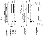
図8は、本発明の実施例6における直流母線電流と三相電圧の関係説明図であり、本発明を、二相変調に適用した実施例である。 FIG. 8 is a diagram illustrating the relationship between the DC bus current and the three-phase voltage in the sixth embodiment of the present invention, and is an embodiment in which the present invention is applied to two-phase modulation.
電力変換部主回路のスイッチ素子の動作回数を減らして素子のエネルギー損失を低減するため、三相のうち一相のスイッチ動作を無くし、残りの2相のみのスイッチ動作により電動機を駆動することが知られており、これを二相変調と呼ぶ。これに対し、実施例1〜4で述べたような通常の変調方式は「三相変調」と呼ばれる。 In order to reduce the energy loss of the element by reducing the number of operation of the switch element of the power converter main circuit, it is possible to eliminate the one-phase switch operation among the three phases and drive the motor by the switch operation of only the remaining two phases. This is known and this is called two-phase modulation. On the other hand, a normal modulation system as described in the first to fourth embodiments is called “three-phase modulation”.
一般的に、二相変調は、電圧最大相V1をスイッチON状態に固定するか、電圧最小相をスイッチOFF状態に固定することで実現される。マイコン6内部の動作としては、最大相あるいは最小相を三角波キャリア信号の振幅範囲外に設定する。これを波形の概観からそれぞれ「最大相張り付き」、「最小相張り付き」と呼ぶ。更に、スイッチ状態が固定されている電圧相を「張り付き相」と呼ぶ。
In general, the two-phase modulation is realized by fixing the maximum voltage phase V1 in the switch ON state or fixing the minimum voltage phase in the switch OFF state. As an internal operation of the
二相変調では、直流母線電流IDCの波形が三相変調方式と比べて変化する。 In the two-phase modulation, the waveform of the DC bus current IDC changes compared to the three-phase modulation method.
図8においては、Vuが最大相張り付きとなっている場合を示している。このとき、直流母線電流IDCには三角波キャリア信号の単調増加期間と単調減少期間にまたがって電圧最大相電流が流れる。このため、見かけ上、最大相電流の通流時間は、線間電圧V12から通常考えられる値の2倍となるため、張り付き相のパルス状電流については、張り付き相を含む線間電圧が、従来の必要条件Vpwの半分以上であれば検出が可能となる。 FIG. 8 shows a case where Vu has a maximum adhesion. At this time, the maximum voltage phase current flows through the DC bus current IDC over the monotonically increasing period and the monotonically decreasing period of the triangular wave carrier signal. For this reason, apparently, the maximum phase current flow time is twice the value normally considered from the line voltage V12. Therefore, for the pulsed current of the stuck phase, the line voltage including the stuck phase is If it is more than half of the necessary condition Vpw, detection is possible.
そのため、通常の環境では張り付き相のパルス状電流は電圧指令補正を行わなくても検出が可能となる。 For this reason, in a normal environment, the pulsed current of the sticking phase can be detected without performing voltage command correction.
しかし、Vpwが大きくなる環境では、張り付き相を含む線間電圧(図8では、V12**)が十分でなく、相電流が検出できない状況が現れる。このとき、実施例1と同じ処理によって中間相を補正することで電流検出が可能となる。また、補償期間における第2の電圧指令飽和の問題についても、実施例2及び3と同じ方法で対応することが出来る。 However, in an environment where Vpw becomes large, a line voltage including a sticking phase (V12 ** in FIG. 8) is not sufficient, and a situation in which a phase current cannot be detected appears. At this time, the current can be detected by correcting the intermediate phase by the same processing as in the first embodiment. Further, the second voltage command saturation problem in the compensation period can be dealt with by the same method as in the second and third embodiments.
以上のように、本実施例6により、2相変調において張り付き相のパルス状電流を検出できないような環境においても、相電流を検出することが可能となり、電力変換装置の損失を減らしつつ高精度な電動機制御が可能となる。 As described above, according to the sixth embodiment, it is possible to detect the phase current even in an environment where the pulsed current of the stuck phase cannot be detected in the two-phase modulation, and it is possible to reduce the loss of the power conversion device with high accuracy. Electric motor control becomes possible.
図9は、本発明の実施例7における直流母線電流と三相電圧の関係説明図である。 FIG. 9 is a diagram illustrating the relationship between the DC bus current and the three-phase voltage in Example 7 of the present invention.
2相変調時においても、調整期間を単位周期の奇数倍とし、検出期間を調整期間の中心と設定することにより精度の向上が可能である。しかし、実施例6で述べたように、パルス状電流が単位周期を跨って流れることを考慮して電流検出を行うと、張り付き相の検出タイミングが実質的に三角波キャリアの単調増加期間あるいは単調減少期間に限られてしまう。このため、実施例4で得られた精度向上の効果が小さくなってしまう。 Even during two-phase modulation, it is possible to improve accuracy by setting the adjustment period to an odd multiple of the unit period and setting the detection period as the center of the adjustment period. However, as described in the sixth embodiment, when the current detection is performed in consideration of the fact that the pulsed current flows over the unit period, the detection timing of the sticky phase is substantially increased or decreased monotonously in the triangular wave carrier. It will be limited to the period. For this reason, the accuracy improvement effect obtained in Example 4 is reduced.
そこで、本実施例7では、三角波キャリア信号の単調増加期間と単調減少期間に跨って電圧最大相電流が流れていることは考慮せず、各単位周囲において(1)式を満たすように電圧指令補正量を決定する。 Therefore, in the seventh embodiment, the voltage command is set so as to satisfy the expression (1) around each unit without considering that the voltage maximum phase current flows over the monotonous increase period and the monotone decrease period of the triangular wave carrier signal. Determine the correction amount.
以上の方法によれば、電力変換装置の損失を減らしつつ、更なる高精度な電流検出を実現することが出来る。 According to the above method, further highly accurate current detection can be realized while reducing the loss of the power conversion device.
電圧上限値Vmaxと電圧下限値Vimの差が必要線間電圧Vpwの2倍より小さく、(28)式が成立する場合には、そもそも(1)式が満たされないため、直流母線電流IDCからの相電流検出は不可能である。 When the difference between the voltage upper limit value Vmax and the voltage lower limit value Vim is smaller than twice the necessary line voltage Vpw and the equation (28) is satisfied, the equation (1) is not satisfied in the first place. Phase current detection is not possible.
Vmax−Vmin<2Vpw…………………………………………………(28)
図2から明らかなように、三角波キャリア周波数を下げることで、同じTpwに対するVpwを小さくすることができる。したがって、(28)式を満たす場合でも、(28)式を満たすような三角波キャリア周波数を設定することで電動機制御が可能となる。
Vmax−Vmin <2Vpw ………………………………………………… (28)
As is apparent from FIG. 2, Vpw for the same Tpw can be reduced by lowering the triangular wave carrier frequency. Therefore, even when the equation (28) is satisfied, the motor can be controlled by setting a triangular wave carrier frequency that satisfies the equation (28).
図10は、本発明の実施例9による電圧指令補正量演算部の処理フロー図である。これは、実施例1の異なる実施形態であり、実施例1では、電圧補正により2相共に検出可能な場合の処理32では、中間相は補正しない(ΔV2=0)としていた。しかし、本実施例9では、ΔV1及びΔV3のうち、必要な補正量が大きくなる側の補正量の一部を中間相に分担させる点が異なっている。以下、図10を用いて説明する。
FIG. 10 is a process flow diagram of the voltage command correction amount calculation unit according to the ninth embodiment of the present invention. This is a different embodiment of the first embodiment. In the first embodiment, the intermediate phase is not corrected (ΔV2 = 0) in the
V12*とV23*を比較し、最大相と最小相で必要な補正量が大きくなる側を判定する。ここではV12*の方が大きい場合を例に説明する。このとき必要な補正量は最大相側Δ1に比べて最小相側ΔV3の方が大きくなる。このときの必要な補正量をV3tとすると、
ΔV3t=(V2*−V3*)−Vpw………………………………………(29)
と求められる。この必要補正量ΔV3tを、最小相と中間相で分担して補正する。例えばある値a(0<a<1の定数。たとえば0.5)を用いて、
ΔV2=−ΔV3t×(1−a)………………………………………………(30)
ΔV3=ΔV3t×a……………………………………………………………(31)
とする。更に中間相を補正した分V12が小さくなるため、
ΔV1=Vpw−(V1*−(V2*+V2))……………………………(32)
と最大相補正量を修正する。
V12 * and V23 * are compared, and the side where the required correction amount becomes larger in the maximum phase and the minimum phase is determined. Here, a case where V12 * is larger will be described as an example. The amount of correction required at this time is larger on the minimum phase side ΔV3 than on the maximum phase side Δ1. If the necessary correction amount at this time is V3t,
ΔV3t = (V2 * −V3 *) − Vpw ………………………………… (29)
Is required. This necessary correction amount ΔV3t is corrected by sharing the minimum phase and the intermediate phase. For example, using a value a (a constant of 0 <a <1; for example, 0.5),
ΔV2 = −ΔV3t × (1-a) ………………………………………… (30)
ΔV3 = ΔV3t × a …………………………………………………………… (31)
And Furthermore, V12 becomes smaller by correcting the intermediate phase.
ΔV1 = Vpw− (V1 * − (V2 * + V2)) ………………………… (32)
And correct the maximum phase correction amount.
なお、ΔV3tが正の場合、電圧補正しなくてもΔV23>Vpwであり、さらにΔV12>ΔV23が分かっているため、全相電圧補正しなくても電流検出が可能である。 When ΔV3t is positive, ΔV23> Vpw is obtained without voltage correction, and ΔV12> ΔV23 is known, and current detection is possible without correcting all-phase voltages.
また、図10には明示していないが、この処理により電圧補正を行った結果、最大相電圧指令値あるいは最小相電圧指令値が電圧上下限を逸脱した場合は、実施例1と同様に処理33または処理34のように補正量を決めればよい。
Although not explicitly shown in FIG. 10, if the maximum phase voltage command value or the minimum phase voltage command value deviates from the upper and lower voltage limits as a result of performing voltage correction by this processing, the same processing as in the first embodiment is performed. What is necessary is just to determine a correction amount like 33 or the
この処理により、電圧補正量を三相に分散させることで、一相ごとの補正量が減り、電流の高周波リプルを軽減し、騒音の抑制及び電動機の運転効率を上げることが出来る。 By dispersing the voltage correction amount in three phases by this processing, the correction amount for each phase is reduced, the high-frequency ripple of current is reduced, noise can be suppressed, and the motor operating efficiency can be increased.
1…直流電源、2…交流電動機、3…電流検出手段、4…マイコン、5…電力変換部主回路、7…電流検出部、8…電圧指令演算部、9…電圧指令補正部、10…電圧指令補正量演算部、11…PWM変換手段。
DESCRIPTION OF
Claims (12)
前記PWMパルスに基づきスイッチ素子を駆動し直流電圧と三相交流電圧との間に電力変換する電力変換器と、
前記電力変換器の主回路の直流母線に流れるパルス状電流を検出する電流検出手段と、
前記三相電圧指令の瞬間値をその大きさの順に並べた場合の最大となる相を最大相、2番目に大きい相を中間相、3番目に大きい相を最小相とするとき、最大相と中間相の線間電圧及び中間相と最小相の線間電圧の、2つの線間電圧がそれぞれ所定値以上となるように、前記最大相と最小相の電圧指令を補正する電圧指令補正手段とを備えた電力変換装置において、
所定の条件において、前記最大相及び/又は最小相の電圧指令のみならず、前記中間相の電圧指令を補正する電圧指令補正手段を備えたことを特徴とする電力変換装置。 Pulse width modulation means for converting the voltage command into a PWM pulse by comparing the three-phase voltage command and the triangular wave carrier signal;
A power converter that drives the switch element based on the PWM pulse to convert power between a DC voltage and a three-phase AC voltage;
Current detection means for detecting a pulsed current flowing in the DC bus of the main circuit of the power converter;
When the instantaneous values of the three-phase voltage commands are arranged in the order of their magnitude, the maximum phase is the maximum phase, the second largest phase is the intermediate phase, and the third largest phase is the minimum phase. Voltage command correction means for correcting the voltage command of the maximum phase and the minimum phase so that the two line voltages of the line voltage of the intermediate phase and the line voltage of the intermediate phase and the minimum phase are equal to or greater than a predetermined value, respectively. In a power conversion device comprising:
A power conversion device comprising voltage command correction means for correcting not only the maximum phase and / or minimum phase voltage command but also the intermediate phase voltage command under a predetermined condition.
前記PWMパルスに基づきスイッチ素子を駆動し直流電圧と三相交流電圧との間に電力変換する電力変換器と、
前記電力変換器の主回路の直流母線に流れるパルス状電流を検出する電流検出手段と、
前記三相電圧指令の瞬間値をその大きさの順に並べた場合の最大となる相を最大相、2番目に大きい相を中間相、3番目に大きい相を最小相とするとき、最大相と中間相の線間電圧及び中間相と最小相の線間電圧の、2つの線間電圧がそれぞれ所定値以上となるように、前記最大相と最小相の電圧指令を補正する電圧指令補正手段とを備えた電力変換装置において、前記最大相あるいは最小相の電圧指令値を補正するとき、電圧補正値の絶対値が大きい側の補正量を一定の割合で削減し、削減された補正量分だけ中間相を補正するよう設定したことを特徴とする電力変換装置。 Pulse width modulation means for converting the voltage command into a PWM pulse by comparing the three-phase voltage command and the triangular wave carrier signal;
A power converter that drives the switch element based on the PWM pulse to convert power between a DC voltage and a three-phase AC voltage;
Current detection means for detecting a pulsed current flowing in the DC bus of the main circuit of the power converter;
When the instantaneous values of the three-phase voltage commands are arranged in the order of their magnitude, the maximum phase is the maximum phase, the second largest phase is the intermediate phase, and the third largest phase is the minimum phase. Voltage command correction means for correcting the voltage command of the maximum phase and the minimum phase so that the two line voltages of the line voltage of the intermediate phase and the line voltage of the intermediate phase and the minimum phase are equal to or greater than a predetermined value, respectively. When correcting the maximum phase or minimum phase voltage command value, the correction amount on the side where the absolute value of the voltage correction value is large is reduced at a constant rate, and only the reduced correction amount is corrected. A power conversion device, which is set to correct an intermediate phase.
前記PWMパルスに基づき電力変換器のスイッチ素子を駆動し直流電圧と三相交流電圧との間に電力変換するステップと、
前記電力変換器の主回路の直流母線に流れるパルス状電流を検出するステップと、
前記三相電圧指令を補正するステップと、
前記三相電圧指令の瞬間値をその大きさの順に並べた場合の最大となる相を最大相、2番目に大きい相を中間相、3番目に大きい相を最小相とするとき、最大相と中間相の線間電圧及び中間相と最小相の線間電圧がともに所定値以上となるように、前記最大相と最小相の電圧指令を補正するステップとを備えた電力変換装置の制御方法において、
前記最大相と最小相の電圧指令を補正するステップで、前記最大相あるいは最小相の電圧指令値を補正したとき、電圧指令値の上限値又は下限値を逸脱するとき、前記最大相及び/又は最小相の電圧指令のみならず、前記中間相の電圧指令を補正するステップを備えたことを特徴とする電力変換装置の制御方法。 Comparing the three-phase voltage command and the triangular wave carrier signal to convert the voltage command into a PWM pulse;
Driving a switch element of a power converter based on the PWM pulse to convert power between a DC voltage and a three-phase AC voltage;
Detecting a pulsed current flowing in a DC bus of a main circuit of the power converter;
Correcting the three-phase voltage command;
When the instantaneous values of the three-phase voltage commands are arranged in the order of their magnitude, the maximum phase is the maximum phase, the second largest phase is the intermediate phase, and the third largest phase is the minimum phase. In the control method of the power conversion device, comprising the step of correcting the voltage command of the maximum phase and the minimum phase so that the line voltage of the intermediate phase and the line voltage of the intermediate phase and the minimum phase are both equal to or higher than a predetermined value. ,
In the step of correcting the voltage command of the maximum phase and the minimum phase in the step of correcting the voltage command value of the maximum phase or the minimum phase, when deviating from the upper limit value or the lower limit value of the voltage command value, the maximum phase and / or A method for controlling a power converter, comprising a step of correcting not only a minimum phase voltage command but also the intermediate phase voltage command.
Priority Applications (5)
| Application Number | Priority Date | Filing Date | Title |
|---|---|---|---|
| JP2009054834A JP5122505B2 (en) | 2009-03-09 | 2009-03-09 | Power conversion apparatus and control method thereof |
| CN201080008248.2A CN102326328B (en) | 2009-03-09 | 2010-02-17 | Power conversion device, and method for controlling thereof |
| EP10750492.0A EP2408100B1 (en) | 2009-03-09 | 2010-02-17 | Power conversion device, and method for controlling thereof |
| PCT/JP2010/000961 WO2010103733A1 (en) | 2009-03-09 | 2010-02-17 | Power conversion device, and method for controlling thereof |
| US13/147,807 US8710781B2 (en) | 2009-03-09 | 2010-02-17 | Power conversion device and method for controlling thereof |
Applications Claiming Priority (1)
| Application Number | Priority Date | Filing Date | Title |
|---|---|---|---|
| JP2009054834A JP5122505B2 (en) | 2009-03-09 | 2009-03-09 | Power conversion apparatus and control method thereof |
Publications (2)
| Publication Number | Publication Date |
|---|---|
| JP2010213407A JP2010213407A (en) | 2010-09-24 |
| JP5122505B2 true JP5122505B2 (en) | 2013-01-16 |
Family
ID=42728032
Family Applications (1)
| Application Number | Title | Priority Date | Filing Date |
|---|---|---|---|
| JP2009054834A Active JP5122505B2 (en) | 2009-03-09 | 2009-03-09 | Power conversion apparatus and control method thereof |
Country Status (5)
| Country | Link |
|---|---|
| US (1) | US8710781B2 (en) |
| EP (1) | EP2408100B1 (en) |
| JP (1) | JP5122505B2 (en) |
| CN (1) | CN102326328B (en) |
| WO (1) | WO2010103733A1 (en) |
Families Citing this family (29)
| Publication number | Priority date | Publication date | Assignee | Title |
|---|---|---|---|---|
| JP5178799B2 (en) | 2010-09-27 | 2013-04-10 | 株式会社東芝 | Motor control device |
| JP2012085379A (en) * | 2010-10-07 | 2012-04-26 | Hitachi Appliances Inc | Motor control system |
| JP5161985B2 (en) | 2011-02-16 | 2013-03-13 | 三菱電機株式会社 | Power conversion device and control device for electric power steering |
| JP5972545B2 (en) * | 2011-09-15 | 2016-08-17 | 株式会社東芝 | Motor control device |
| JP5783066B2 (en) * | 2012-01-26 | 2015-09-24 | ダイキン工業株式会社 | Power converter control device |
| JP5783064B2 (en) * | 2012-01-26 | 2015-09-24 | ダイキン工業株式会社 | Power converter control device |
| JP5783065B2 (en) * | 2012-01-26 | 2015-09-24 | ダイキン工業株式会社 | Power converter control device |
| CN104221274B (en) * | 2012-04-12 | 2016-12-28 | 株式会社日立制作所 | Three-phase synchronous motor driving means |
| JP2014011944A (en) * | 2012-07-03 | 2014-01-20 | Mitsubishi Electric Corp | Power conversion system and power conversion method |
| JP6011261B2 (en) * | 2012-11-14 | 2016-10-19 | 富士電機株式会社 | Three-phase PWM inverter device and motor control device using the same |
| JP5908424B2 (en) * | 2013-03-25 | 2016-04-26 | 日立オートモティブシステムズステアリング株式会社 | Motor control device and power steering device |
| JP5983567B2 (en) * | 2013-09-10 | 2016-08-31 | トヨタ自動車株式会社 | Electric motor control device |
| JP5920300B2 (en) * | 2013-09-18 | 2016-05-18 | 株式会社デンソー | Power conversion device and electric power steering device using the same |
| JP5839011B2 (en) * | 2013-09-18 | 2016-01-06 | 株式会社デンソー | Power conversion device and electric power steering device using the same |
| CN105794104B (en) * | 2013-12-03 | 2018-06-22 | 日立汽车系统株式会社 | Motor drive |
| JP6327010B2 (en) * | 2014-06-26 | 2018-05-23 | 富士電機株式会社 | Inverter control device |
| JP6516857B2 (en) * | 2015-10-13 | 2019-05-22 | 三菱電機株式会社 | Control device for alternating current rotating machine and electric power steering device provided with the same |
| EP3439163B1 (en) * | 2016-03-28 | 2022-08-31 | Mitsubishi Electric Corporation | Power converter |
| US11267503B2 (en) * | 2017-01-11 | 2022-03-08 | Mitsubishi Electric Cornoration | Motor control device |
| US11063544B2 (en) | 2017-07-04 | 2021-07-13 | Mitsubishi Electric Corporation | Inverter device and electric power steering apparatus |
| JP2019075964A (en) * | 2017-10-19 | 2019-05-16 | アイシン精機株式会社 | Motor controller |
| JP6982519B2 (en) * | 2018-03-07 | 2021-12-17 | サンデンホールディングス株式会社 | Power converter |
| JP7064932B2 (en) * | 2018-04-17 | 2022-05-11 | 日立Astemo株式会社 | Inverter control device, inverter control method, inverter control program |
| JP2020156290A (en) * | 2019-03-22 | 2020-09-24 | 日本電産株式会社 | Motor drive controller, motor system, and blower |
| JP7221802B2 (en) * | 2019-06-04 | 2023-02-14 | サンデン株式会社 | power converter |
| CN110581663B (en) * | 2019-10-16 | 2022-04-01 | 南京理工大学 | Phase compensation device and method of Vienna rectifier under low carrier ratio |
| JP7406446B2 (en) * | 2020-04-28 | 2023-12-27 | ローム株式会社 | motor control circuit |
| CN113098454B (en) * | 2021-03-31 | 2023-03-31 | 上海电气风电集团股份有限公司 | PWM signal generation method, single-phase PWM signal generation module and three-phase PWM signal generation module |
| CN116298491B (en) * | 2023-05-11 | 2023-07-28 | 昆山迈致治具科技有限公司 | Pulse type direct current measurement method applied to backlight current detection of display screen |
Family Cites Families (14)
| Publication number | Priority date | Publication date | Assignee | Title |
|---|---|---|---|---|
| EP0638457B1 (en) * | 1993-08-10 | 1999-03-03 | Toyota Jidosha Kabushiki Kaisha | Apparatus for driving and controlling synchronous motor using permanent magnets as its field system |
| JPH0819263A (en) | 1994-06-30 | 1996-01-19 | Meidensha Corp | Output current detector of pwm inverter |
| JP3625901B2 (en) * | 1995-06-30 | 2005-03-02 | 三菱電機株式会社 | Method and apparatus for automatically optimizing servo control system |
| US5790396A (en) * | 1995-12-19 | 1998-08-04 | Kabushiki Kaisha Toshiba | Neutral point clamped (NPC) inverter control system |
| JP3664040B2 (en) * | 2000-05-17 | 2005-06-22 | 日産自動車株式会社 | PWM inverter for motor control |
| KR100674423B1 (en) * | 2001-01-19 | 2007-01-29 | 엘지전자 주식회사 | Transmitting/receiving system and data processing method |
| KR100425851B1 (en) * | 2001-05-10 | 2004-04-03 | 엘지산전 주식회사 | Method for measuring three-phase current with single current sensor |
| US6735537B2 (en) * | 2002-03-15 | 2004-05-11 | Motorola, Inc. | Procedure for measuring the current in each phase of a three-phase device via single current sensor |
| JP4069741B2 (en) | 2002-12-19 | 2008-04-02 | 株式会社日立製作所 | Pulse width modulation method and power converter |
| JP3951975B2 (en) * | 2003-07-22 | 2007-08-01 | 株式会社日立製作所 | AC motor control device, AC motor control method and module |
| JP4529488B2 (en) * | 2004-03-05 | 2010-08-25 | 三菱電機株式会社 | Phase voltage command value correction method and motor control device using this phase voltage command value correction method |
| JP4505725B2 (en) * | 2004-03-18 | 2010-07-21 | 富士電機システムズ株式会社 | Three-phase inverter device |
| JPWO2006112033A1 (en) * | 2005-04-15 | 2008-11-27 | 株式会社日立製作所 | AC motor controller |
| JP4866216B2 (en) * | 2006-11-22 | 2012-02-01 | 株式会社日立製作所 | Power converter |
-
2009
- 2009-03-09 JP JP2009054834A patent/JP5122505B2/en active Active
-
2010
- 2010-02-17 WO PCT/JP2010/000961 patent/WO2010103733A1/en active Application Filing
- 2010-02-17 US US13/147,807 patent/US8710781B2/en active Active
- 2010-02-17 CN CN201080008248.2A patent/CN102326328B/en active Active
- 2010-02-17 EP EP10750492.0A patent/EP2408100B1/en active Active
Also Published As
| Publication number | Publication date |
|---|---|
| JP2010213407A (en) | 2010-09-24 |
| US8710781B2 (en) | 2014-04-29 |
| CN102326328A (en) | 2012-01-18 |
| EP2408100B1 (en) | 2020-08-19 |
| CN102326328B (en) | 2014-04-09 |
| EP2408100A4 (en) | 2017-06-28 |
| WO2010103733A1 (en) | 2010-09-16 |
| EP2408100A1 (en) | 2012-01-18 |
| US20110292700A1 (en) | 2011-12-01 |
Similar Documents
| Publication | Publication Date | Title |
|---|---|---|
| JP5122505B2 (en) | Power conversion apparatus and control method thereof | |
| US8674652B2 (en) | Motor control device | |
| JP4749874B2 (en) | Power conversion device and motor drive device using the same | |
| JP6045765B1 (en) | Power conversion device and vehicle drive system using the same | |
| JP4866216B2 (en) | Power converter | |
| US9362840B2 (en) | Power conversion device | |
| US9130481B2 (en) | Power converting appartatus | |
| US11218107B2 (en) | Control device for power converter | |
| US20080180095A1 (en) | Method and related device for estimating the currents flowing in windings of a poly-phase electrical load at a certain instant | |
| US20180159458A1 (en) | Control apparatus and control method | |
| TW200924366A (en) | Matrix converter | |
| JP6293401B2 (en) | Motor controller for air conditioner and air conditioner | |
| US11658600B2 (en) | Motor controller, motor system and method for controlling motor | |
| JP5104083B2 (en) | Power conversion device and power conversion method | |
| JP2012182874A (en) | Motor control device | |
| JP2017205017A (en) | Motor control device of air conditioner, and air conditioner | |
| JP2022090317A (en) | Inverter control device, and control method of inverter | |
| JP5223521B2 (en) | Power converter | |
| US11716045B2 (en) | Motor controller, motor system and method for controlling motor | |
| CN110557078B (en) | Motor control device, control method thereof, and computer-readable medium | |
| JP2014230382A (en) | Motor drive device |
Legal Events
| Date | Code | Title | Description |
|---|---|---|---|
| A621 | Written request for application examination |
Free format text: JAPANESE INTERMEDIATE CODE: A621 Effective date: 20110214 |
|
| TRDD | Decision of grant or rejection written | ||
| A01 | Written decision to grant a patent or to grant a registration (utility model) |
Free format text: JAPANESE INTERMEDIATE CODE: A01 Effective date: 20121016 |
|
| A01 | Written decision to grant a patent or to grant a registration (utility model) |
Free format text: JAPANESE INTERMEDIATE CODE: A01 |
|
| A61 | First payment of annual fees (during grant procedure) |
Free format text: JAPANESE INTERMEDIATE CODE: A61 Effective date: 20121024 |
|
| FPAY | Renewal fee payment (event date is renewal date of database) |
Free format text: PAYMENT UNTIL: 20151102 Year of fee payment: 3 |
|
| R150 | Certificate of patent or registration of utility model |
Free format text: JAPANESE INTERMEDIATE CODE: R150 Ref document number: 5122505 Country of ref document: JP Free format text: JAPANESE INTERMEDIATE CODE: R150 |