JP5121103B2 - Semiconductor device, method for manufacturing semiconductor device, and electric appliance - Google Patents
Semiconductor device, method for manufacturing semiconductor device, and electric appliance Download PDFInfo
- Publication number
- JP5121103B2 JP5121103B2 JP2001276341A JP2001276341A JP5121103B2 JP 5121103 B2 JP5121103 B2 JP 5121103B2 JP 2001276341 A JP2001276341 A JP 2001276341A JP 2001276341 A JP2001276341 A JP 2001276341A JP 5121103 B2 JP5121103 B2 JP 5121103B2
- Authority
- JP
- Japan
- Prior art keywords
- substrate
- thin film
- film
- insulating film
- forming
- Prior art date
- Legal status (The legal status is an assumption and is not a legal conclusion. Google has not performed a legal analysis and makes no representation as to the accuracy of the status listed.)
- Expired - Fee Related
Links
- 239000004065 semiconductor Substances 0.000 title claims description 106
- 238000000034 method Methods 0.000 title claims description 80
- 238000004519 manufacturing process Methods 0.000 title claims description 59
- 239000010408 film Substances 0.000 claims description 421
- 239000000758 substrate Substances 0.000 claims description 406
- 239000010409 thin film Substances 0.000 claims description 361
- 239000000853 adhesive Substances 0.000 claims description 53
- 230000001070 adhesive effect Effects 0.000 claims description 53
- 239000000463 material Substances 0.000 claims description 51
- 238000005520 cutting process Methods 0.000 claims description 25
- 238000005530 etching Methods 0.000 claims description 25
- 238000005498 polishing Methods 0.000 claims description 6
- 239000012528 membrane Substances 0.000 claims 2
- 239000010410 layer Substances 0.000 description 141
- 239000004973 liquid crystal related substance Substances 0.000 description 65
- 239000012535 impurity Substances 0.000 description 37
- 239000011159 matrix material Substances 0.000 description 35
- 229910021417 amorphous silicon Inorganic materials 0.000 description 24
- 238000000137 annealing Methods 0.000 description 22
- 230000008569 process Effects 0.000 description 22
- 238000010438 heat treatment Methods 0.000 description 21
- OAICVXFJPJFONN-UHFFFAOYSA-N Phosphorus Chemical compound [P] OAICVXFJPJFONN-UHFFFAOYSA-N 0.000 description 20
- 125000004429 atom Chemical group 0.000 description 20
- 238000010586 diagram Methods 0.000 description 20
- 230000003071 parasitic effect Effects 0.000 description 20
- 229910052698 phosphorus Inorganic materials 0.000 description 20
- 239000011574 phosphorus Substances 0.000 description 20
- 229910021419 crystalline silicon Inorganic materials 0.000 description 18
- 239000001257 hydrogen Substances 0.000 description 18
- 229910052739 hydrogen Inorganic materials 0.000 description 18
- VYPSYNLAJGMNEJ-UHFFFAOYSA-N silicon dioxide Inorganic materials O=[Si]=O VYPSYNLAJGMNEJ-UHFFFAOYSA-N 0.000 description 18
- XUIMIQQOPSSXEZ-UHFFFAOYSA-N Silicon Chemical compound [Si] XUIMIQQOPSSXEZ-UHFFFAOYSA-N 0.000 description 17
- 239000011229 interlayer Substances 0.000 description 17
- 229910052710 silicon Inorganic materials 0.000 description 17
- 239000010703 silicon Substances 0.000 description 17
- UFHFLCQGNIYNRP-UHFFFAOYSA-N Hydrogen Chemical compound [H][H] UFHFLCQGNIYNRP-UHFFFAOYSA-N 0.000 description 16
- 230000015572 biosynthetic process Effects 0.000 description 16
- 229910052581 Si3N4 Inorganic materials 0.000 description 14
- 229920005989 resin Polymers 0.000 description 14
- 239000011347 resin Substances 0.000 description 14
- HQVNEWCFYHHQES-UHFFFAOYSA-N silicon nitride Chemical compound N12[Si]34N5[Si]62N3[Si]51N64 HQVNEWCFYHHQES-UHFFFAOYSA-N 0.000 description 14
- 125000006850 spacer group Chemical group 0.000 description 14
- 230000001681 protective effect Effects 0.000 description 13
- IJGRMHOSHXDMSA-UHFFFAOYSA-N Atomic nitrogen Chemical compound N#N IJGRMHOSHXDMSA-UHFFFAOYSA-N 0.000 description 12
- ZOXJGFHDIHLPTG-UHFFFAOYSA-N Boron Chemical compound [B] ZOXJGFHDIHLPTG-UHFFFAOYSA-N 0.000 description 12
- PXHVJJICTQNCMI-UHFFFAOYSA-N Nickel Chemical compound [Ni] PXHVJJICTQNCMI-UHFFFAOYSA-N 0.000 description 12
- 229910052796 boron Inorganic materials 0.000 description 12
- 238000002425 crystallisation Methods 0.000 description 12
- 230000008025 crystallization Effects 0.000 description 12
- 239000011521 glass Substances 0.000 description 11
- 238000002161 passivation Methods 0.000 description 11
- NIXOWILDQLNWCW-UHFFFAOYSA-N acrylic acid group Chemical group C(C=C)(=O)O NIXOWILDQLNWCW-UHFFFAOYSA-N 0.000 description 10
- 239000007789 gas Substances 0.000 description 10
- 229910052751 metal Inorganic materials 0.000 description 10
- 239000002184 metal Substances 0.000 description 10
- 229920001721 polyimide Polymers 0.000 description 10
- 239000010936 titanium Substances 0.000 description 10
- 230000000694 effects Effects 0.000 description 9
- 239000000945 filler Substances 0.000 description 9
- 239000012212 insulator Substances 0.000 description 9
- 239000010453 quartz Substances 0.000 description 9
- 229910052814 silicon oxide Inorganic materials 0.000 description 9
- 239000004642 Polyimide Substances 0.000 description 8
- QVQLCTNNEUAWMS-UHFFFAOYSA-N barium oxide Chemical compound [Ba]=O QVQLCTNNEUAWMS-UHFFFAOYSA-N 0.000 description 8
- 239000003054 catalyst Substances 0.000 description 8
- 238000005984 hydrogenation reaction Methods 0.000 description 8
- 238000005224 laser annealing Methods 0.000 description 8
- 150000004767 nitrides Chemical class 0.000 description 8
- 230000010355 oscillation Effects 0.000 description 8
- 229910052760 oxygen Inorganic materials 0.000 description 8
- 239000003566 sealing material Substances 0.000 description 8
- 229910052782 aluminium Inorganic materials 0.000 description 7
- XAGFODPZIPBFFR-UHFFFAOYSA-N aluminium Chemical compound [Al] XAGFODPZIPBFFR-UHFFFAOYSA-N 0.000 description 7
- 238000004544 sputter deposition Methods 0.000 description 7
- 239000012298 atmosphere Substances 0.000 description 6
- QVGXLLKOCUKJST-UHFFFAOYSA-N atomic oxygen Chemical compound [O] QVGXLLKOCUKJST-UHFFFAOYSA-N 0.000 description 6
- 150000001875 compounds Chemical class 0.000 description 6
- 229910052759 nickel Inorganic materials 0.000 description 6
- 229910052757 nitrogen Inorganic materials 0.000 description 6
- 239000001301 oxygen Substances 0.000 description 6
- 229910021420 polycrystalline silicon Inorganic materials 0.000 description 6
- 229920002620 polyvinyl fluoride Polymers 0.000 description 6
- 239000010935 stainless steel Substances 0.000 description 6
- 229910001220 stainless steel Inorganic materials 0.000 description 6
- 239000011248 coating agent Substances 0.000 description 5
- 238000000576 coating method Methods 0.000 description 5
- 230000010354 integration Effects 0.000 description 5
- 239000000565 sealant Substances 0.000 description 5
- 238000001039 wet etching Methods 0.000 description 5
- XKRFYHLGVUSROY-UHFFFAOYSA-N Argon Chemical compound [Ar] XKRFYHLGVUSROY-UHFFFAOYSA-N 0.000 description 4
- 229920002799 BoPET Polymers 0.000 description 4
- RYGMFSIKBFXOCR-UHFFFAOYSA-N Copper Chemical compound [Cu] RYGMFSIKBFXOCR-UHFFFAOYSA-N 0.000 description 4
- KRHYYFGTRYWZRS-UHFFFAOYSA-N Fluorane Chemical compound F KRHYYFGTRYWZRS-UHFFFAOYSA-N 0.000 description 4
- XEEYBQQBJWHFJM-UHFFFAOYSA-N Iron Chemical compound [Fe] XEEYBQQBJWHFJM-UHFFFAOYSA-N 0.000 description 4
- 239000005041 Mylar™ Substances 0.000 description 4
- KDLHZDBZIXYQEI-UHFFFAOYSA-N Palladium Chemical compound [Pd] KDLHZDBZIXYQEI-UHFFFAOYSA-N 0.000 description 4
- XYFCBTPGUUZFHI-UHFFFAOYSA-N Phosphine Chemical compound P XYFCBTPGUUZFHI-UHFFFAOYSA-N 0.000 description 4
- 239000004372 Polyvinyl alcohol Substances 0.000 description 4
- XLOMVQKBTHCTTD-UHFFFAOYSA-N Zinc monoxide Chemical compound [Zn]=O XLOMVQKBTHCTTD-UHFFFAOYSA-N 0.000 description 4
- UMIVXZPTRXBADB-UHFFFAOYSA-N benzocyclobutene Chemical compound C1=CC=C2CCC2=C1 UMIVXZPTRXBADB-UHFFFAOYSA-N 0.000 description 4
- DQXBYHZEEUGOBF-UHFFFAOYSA-N but-3-enoic acid;ethene Chemical compound C=C.OC(=O)CC=C DQXBYHZEEUGOBF-UHFFFAOYSA-N 0.000 description 4
- 230000003197 catalytic effect Effects 0.000 description 4
- 239000011651 chromium Substances 0.000 description 4
- 229910052802 copper Inorganic materials 0.000 description 4
- 239000010949 copper Substances 0.000 description 4
- 239000013078 crystal Substances 0.000 description 4
- 239000005038 ethylene vinyl acetate Substances 0.000 description 4
- 239000011152 fibreglass Substances 0.000 description 4
- 230000006870 function Effects 0.000 description 4
- 238000005247 gettering Methods 0.000 description 4
- 229910003437 indium oxide Inorganic materials 0.000 description 4
- PJXISJQVUVHSOJ-UHFFFAOYSA-N indium(iii) oxide Chemical compound [O-2].[O-2].[O-2].[In+3].[In+3] PJXISJQVUVHSOJ-UHFFFAOYSA-N 0.000 description 4
- 238000002347 injection Methods 0.000 description 4
- 239000007924 injection Substances 0.000 description 4
- 238000005468 ion implantation Methods 0.000 description 4
- 150000002500 ions Chemical class 0.000 description 4
- 238000005268 plasma chemical vapour deposition Methods 0.000 description 4
- 229920003023 plastic Polymers 0.000 description 4
- 229920001200 poly(ethylene-vinyl acetate) Polymers 0.000 description 4
- 229920002037 poly(vinyl butyral) polymer Polymers 0.000 description 4
- 229920006267 polyester film Polymers 0.000 description 4
- 229920002451 polyvinyl alcohol Polymers 0.000 description 4
- 229920000915 polyvinyl chloride Polymers 0.000 description 4
- 239000004800 polyvinyl chloride Substances 0.000 description 4
- 230000001737 promoting effect Effects 0.000 description 4
- 238000004151 rapid thermal annealing Methods 0.000 description 4
- 238000000926 separation method Methods 0.000 description 4
- 239000002356 single layer Substances 0.000 description 4
- 239000000126 substance Substances 0.000 description 4
- 229910052715 tantalum Inorganic materials 0.000 description 4
- GUVRBAGPIYLISA-UHFFFAOYSA-N tantalum atom Chemical compound [Ta] GUVRBAGPIYLISA-UHFFFAOYSA-N 0.000 description 4
- 230000008859 change Effects 0.000 description 3
- 239000004020 conductor Substances 0.000 description 3
- 230000006866 deterioration Effects 0.000 description 3
- 230000005284 excitation Effects 0.000 description 3
- 238000000227 grinding Methods 0.000 description 3
- AMGQUBHHOARCQH-UHFFFAOYSA-N indium;oxotin Chemical compound [In].[Sn]=O AMGQUBHHOARCQH-UHFFFAOYSA-N 0.000 description 3
- 239000004033 plastic Substances 0.000 description 3
- 239000012780 transparent material Substances 0.000 description 3
- VYZAMTAEIAYCRO-UHFFFAOYSA-N Chromium Chemical compound [Cr] VYZAMTAEIAYCRO-UHFFFAOYSA-N 0.000 description 2
- GYHNNYVSQQEPJS-UHFFFAOYSA-N Gallium Chemical compound [Ga] GYHNNYVSQQEPJS-UHFFFAOYSA-N 0.000 description 2
- ZOKXTWBITQBERF-UHFFFAOYSA-N Molybdenum Chemical compound [Mo] ZOKXTWBITQBERF-UHFFFAOYSA-N 0.000 description 2
- 239000004952 Polyamide Substances 0.000 description 2
- BQCADISMDOOEFD-UHFFFAOYSA-N Silver Chemical compound [Ag] BQCADISMDOOEFD-UHFFFAOYSA-N 0.000 description 2
- 229910001362 Ta alloys Inorganic materials 0.000 description 2
- ATJFFYVFTNAWJD-UHFFFAOYSA-N Tin Chemical compound [Sn] ATJFFYVFTNAWJD-UHFFFAOYSA-N 0.000 description 2
- RTAQQCXQSZGOHL-UHFFFAOYSA-N Titanium Chemical compound [Ti] RTAQQCXQSZGOHL-UHFFFAOYSA-N 0.000 description 2
- 229910001080 W alloy Inorganic materials 0.000 description 2
- LEVVHYCKPQWKOP-UHFFFAOYSA-N [Si].[Ge] Chemical compound [Si].[Ge] LEVVHYCKPQWKOP-UHFFFAOYSA-N 0.000 description 2
- 238000001994 activation Methods 0.000 description 2
- 229910045601 alloy Inorganic materials 0.000 description 2
- 239000000956 alloy Substances 0.000 description 2
- 150000001408 amides Chemical class 0.000 description 2
- 229910052786 argon Inorganic materials 0.000 description 2
- IVHJCRXBQPGLOV-UHFFFAOYSA-N azanylidynetungsten Chemical compound [W]#N IVHJCRXBQPGLOV-UHFFFAOYSA-N 0.000 description 2
- 239000000919 ceramic Substances 0.000 description 2
- 229910052804 chromium Inorganic materials 0.000 description 2
- 229910017052 cobalt Inorganic materials 0.000 description 2
- 239000010941 cobalt Substances 0.000 description 2
- GUTLYIVDDKVIGB-UHFFFAOYSA-N cobalt atom Chemical compound [Co] GUTLYIVDDKVIGB-UHFFFAOYSA-N 0.000 description 2
- 230000007547 defect Effects 0.000 description 2
- 238000006356 dehydrogenation reaction Methods 0.000 description 2
- 238000001312 dry etching Methods 0.000 description 2
- 238000005401 electroluminescence Methods 0.000 description 2
- 238000005516 engineering process Methods 0.000 description 2
- 239000003822 epoxy resin Substances 0.000 description 2
- 238000001704 evaporation Methods 0.000 description 2
- 239000011888 foil Substances 0.000 description 2
- 229910052733 gallium Inorganic materials 0.000 description 2
- 229910052732 germanium Inorganic materials 0.000 description 2
- GNPVGFCGXDBREM-UHFFFAOYSA-N germanium atom Chemical compound [Ge] GNPVGFCGXDBREM-UHFFFAOYSA-N 0.000 description 2
- 229910052736 halogen Inorganic materials 0.000 description 2
- 150000002367 halogens Chemical class 0.000 description 2
- 239000003779 heat-resistant material Substances 0.000 description 2
- 230000005525 hole transport Effects 0.000 description 2
- 150000002431 hydrogen Chemical class 0.000 description 2
- 229910052742 iron Inorganic materials 0.000 description 2
- 239000011133 lead Substances 0.000 description 2
- 229910052750 molybdenum Inorganic materials 0.000 description 2
- 239000011733 molybdenum Substances 0.000 description 2
- 229910021421 monocrystalline silicon Inorganic materials 0.000 description 2
- 239000000178 monomer Substances 0.000 description 2
- 239000012299 nitrogen atmosphere Substances 0.000 description 2
- 229910052763 palladium Inorganic materials 0.000 description 2
- 230000000737 periodic effect Effects 0.000 description 2
- 229910000073 phosphorus hydride Inorganic materials 0.000 description 2
- 238000009832 plasma treatment Methods 0.000 description 2
- 229920002647 polyamide Polymers 0.000 description 2
- 229920000647 polyepoxide Polymers 0.000 description 2
- 229920000642 polymer Polymers 0.000 description 2
- 229920005591 polysilicon Polymers 0.000 description 2
- 239000002994 raw material Substances 0.000 description 2
- 238000007789 sealing Methods 0.000 description 2
- LIVNPJMFVYWSIS-UHFFFAOYSA-N silicon monoxide Chemical class [Si-]#[O+] LIVNPJMFVYWSIS-UHFFFAOYSA-N 0.000 description 2
- 229920002050 silicone resin Polymers 0.000 description 2
- 229910052709 silver Inorganic materials 0.000 description 2
- 239000004332 silver Substances 0.000 description 2
- 238000009751 slip forming Methods 0.000 description 2
- 238000012719 thermal polymerization Methods 0.000 description 2
- 229920001187 thermosetting polymer Polymers 0.000 description 2
- 229910052718 tin Inorganic materials 0.000 description 2
- 239000011135 tin Substances 0.000 description 2
- XOLBLPGZBRYERU-UHFFFAOYSA-N tin dioxide Chemical compound O=[Sn]=O XOLBLPGZBRYERU-UHFFFAOYSA-N 0.000 description 2
- 229910001887 tin oxide Inorganic materials 0.000 description 2
- 229910052719 titanium Inorganic materials 0.000 description 2
- WFKWXMTUELFFGS-UHFFFAOYSA-N tungsten Chemical compound [W] WFKWXMTUELFFGS-UHFFFAOYSA-N 0.000 description 2
- 229910052721 tungsten Inorganic materials 0.000 description 2
- 239000010937 tungsten Substances 0.000 description 2
- 239000011787 zinc oxide Substances 0.000 description 2
- 229920001651 Cyanoacrylate Polymers 0.000 description 1
- 239000004593 Epoxy Substances 0.000 description 1
- JOYRKODLDBILNP-UHFFFAOYSA-N Ethyl urethane Chemical compound CCOC(N)=O JOYRKODLDBILNP-UHFFFAOYSA-N 0.000 description 1
- MWCLLHOVUTZFKS-UHFFFAOYSA-N Methyl cyanoacrylate Chemical compound COC(=O)C(=C)C#N MWCLLHOVUTZFKS-UHFFFAOYSA-N 0.000 description 1
- 239000003990 capacitor Substances 0.000 description 1
- ZOCHARZZJNPSEU-UHFFFAOYSA-N diboron Chemical compound B#B ZOCHARZZJNPSEU-UHFFFAOYSA-N 0.000 description 1
- 239000003292 glue Substances 0.000 description 1
- 230000006872 improvement Effects 0.000 description 1
- 230000003287 optical effect Effects 0.000 description 1
- 238000000059 patterning Methods 0.000 description 1
- 230000035699 permeability Effects 0.000 description 1
- 230000010287 polarization Effects 0.000 description 1
- 238000007517 polishing process Methods 0.000 description 1
- 208000024891 symptom Diseases 0.000 description 1
- 238000007725 thermal activation Methods 0.000 description 1
- XLYOFNOQVPJJNP-UHFFFAOYSA-N water Substances O XLYOFNOQVPJJNP-UHFFFAOYSA-N 0.000 description 1
- 239000002023 wood Substances 0.000 description 1
Images


Landscapes
- Liquid Crystal (AREA)
- Thin Film Transistor (AREA)
- Devices For Indicating Variable Information By Combining Individual Elements (AREA)
Description
【0001】
【発明の属する技術分野】
半導体装置の作製方法に関し、特に、薄くてフレキシブルな(可撓性を有する)半導体装置を作製する方法に関する。また、異なる層に絶縁膜を介して形成された配線間に生じる寄生容量を低減する方法に関する。なお、本明細書において半導体装置とは、半導体特性を利用することで機能する装置全般を指し、特に本発明は、絶縁体上に半導体層を形成したSOI(Silicon On Insulator)構造の素子を用いた集積回路、薄膜トランジスタ(TFT)を用いて構成されたアクティブマトリクス型液晶表示装置、アクティブマトリクス型EL表示装置等に好適に適用できる。ここで、本明細書において、薄膜デバイスとは、半導体薄膜を用いて構成した薄膜トランジスタ(TFT)および配線、導電層、抵抗もしくは容量素子等のうち、少なくとも1つを含む電子デバイスのことを指す。
【0002】
【従来の技術】
半導体装置の一つとして、絶縁体上に半導体層を形成したSOI構造の素子を用いた集積回路がある。半導体層が絶縁体上に形成されているため、寄生容量が少なく、高速動作が可能である。
【0003】
半導体装置の一つとして、アクティブマトリクス型液晶表示装置がある。アクティブマトリクス型液晶表示装置は、画素のスイッチング素子として用いられる薄膜トランジスタ(TFT)を形成した基板(TFT形成基板)と、対向電極を形成した基板(対向基板)とを貼り合わせ、間隙に液晶を注入した構造が主流である。このアクティブマトリクス型液晶表示装置は、ガラス等の透明基板上に形成されたTFTにより、液晶へ印加する電圧を1画素ごとに制御できるため、画像が鮮明であり、OA機器やTV等に広く用いられている。
【0004】
また、半導体装置の一つとして、アクティブマトリクス型EL表示装置が知られている。アクティブマトリクス型EL表示装置は、2枚の電極の間にEL材料を挟みこんだ構造をしており、電流を流して発光させる。複数個の画素トランジスタを用いて、EL材料に流す電流を一画素ごとに制御できるため、画像が鮮明である。
【0005】
これらの半導体装置は、ますます微細化され集積度が向上されている。半導体装置の配線間に生じる寄生容量は、電気信号に伝播遅延を引き起こし、電気回路の高速動作や電気信号の正確な伝播を妨げる原因となっている。配線間に生じる寄生容量は、同じ層に形成された配線間に生じるものと、異なる層に絶縁膜を介して形成された配線間に生じるものとがある。
【0006】
集積度が向上すると、同じ層に形成された配線間の距離は小さくなり、寄生容量が増える。同じ層に形成された配線間の寄生容量を減らすには、配線を異なる層に移動させればよい。つまり、多層配線化して同じ層の配線の集積度を下げる。そうすると、異なる層に絶縁膜を介して形成された配線間に生じる寄生容量を減らすことは、半導体装置全体の集積度の向上に寄与することになる。
【0007】
そこで、異なる層に絶縁膜を介して形成された配線間に生じる寄生容量を低減するために、絶縁膜を厚くして配線間の距離を大きくとる、誘電率の低い絶縁膜を使う、等の方法がとられてきた。しかし、絶縁膜を厚くすると、配線間に導通をとるために絶縁膜にあける開孔部が開けにくくなるだけでなく、例えば、スパッタで形成する導電層が開孔部の内部において断線する、もしくは十分な膜厚が確保できないため、抵抗が大きくなる、等の問題が起こる場合がある。また、誘電率の低い絶縁膜は、耐熱性や透水性等の膜質に関する問題、エッチングによる寸法変化等の加工上の問題が生じる可能性がある。例えば、厚さ1μmのアクリルの場合、エッチング条件にもよるが、穴径が約1μm大きくなることもあり、半導体装置全体の集積度を向上する上で障害となる場合がある。
【0008】
また、配線を形成する導電層の形成順序を変える方法もある。ここで、素子間の導通をとる配線を二層有する集積回路をトップゲート型トランジスタで構成する場合、成膜順に述べると、通常次のような構成になる。活性層、第一の絶縁膜(ゲート絶縁膜)、第一の導電層(ゲート電極)、第二の絶縁膜(第一層間絶縁膜)、第二の導電層(第一配線)、第三の絶縁膜(第二層間絶縁膜)、第三の導電層(第二配線)。
【0009】
それを変えて、第一の導電層(第二配線)、第一の絶縁膜(下部絶縁膜)、活性層、第二の絶縁膜(ゲート絶縁膜)、第二の導電層(ゲート電極)、第三の絶縁膜(第一層間絶縁膜)、第三の導電層(第一配線)、と構成すると、第一配線と第二配線の間の距離が大きくなり、その間に形成される寄生容量を少なくすることができる。
【0010】
この場合、第一配線と第二配線の距離は大きくなるが、例えば、活性層を介することで、開孔、導通の問題は回避できる。しかし、同じ第二配線でも、後者の場合、後で形成する活性層の成膜温度や注入した不純物の熱活性化温度に耐えられるものを使用しなければならず、前者の場合と後者の場合で必ずしも同じ材料を使うことができない。例えば、Alは抵抗率の低い配線材料としてよく用いられるが、耐熱性が低いので、後者の場合には使えない。
【0011】
なお、本明細書中において「電極」とは「配線」の一部であり、説明の便宜上、「配線」と「電極」とを使い分けるが、「電極」という言葉に「配線」は常に含められているものとする。
【0012】
【発明が解決しようとする課題】
上記したような半導体装置は近年、携帯機器等に用いられ、薄型化、軽量化、フレキシビリティ(可撓性)が求められている。半導体装置の厚さの大部分は基板の厚さであり、薄型化、軽量化するには、基板を薄くすればよい。しかし、基板を薄くすれば、作製時に基板がそって写真製版工程でのトラブル原因になる他、基板搬送時に基板割れが起こりやすくなるなど、作製が困難である。そこで、透明なプラスチック基板等の上に半導体装置を作製できれば、軽くてフレキシブルな表示装置を作製できるが、プラスチック基板の耐熱性等の問題でまだ実現していない。
【0013】
また、異なる層に絶縁膜を介して形成された配線間に生じる寄生容量を低減し、Al等、耐熱性が低くて使えなかった配線材料を使えるように、電気回路の高速動作や電気信号の正確な伝播を行えるようにする。
【0014】
【課題を解決するための手段】
そこで、本発明者は、作製時には十分な耐熱性、強度を持った基板上に薄膜デバイスを作製し、前記基板を取り除く方法を考えた。まず、第一の基板に薄膜デバイスを形成し、第二の基板に接着する。この状態で第一の基板と第二の基板の間に薄膜デバイスが存在する。そして、第二の基板に保持された状態で、薄膜デバイスを残して第一の基板を取り除き、第二の基板に保持された薄膜デバイスに到達する開孔部を設け、前記開孔部を介して前記薄膜デバイスに接するように導電層を形成するなど必要な加工を行ってから、第二の基板も取り除く。
【0015】
さらに本発明においては、薄膜デバイスが形成されていない領域の一部に接着材を塗布することで、第一の基板と第二の基板を接着することを特徴としている。もしくは、薄膜デバイスが形成されていない領域の一部に接着材を塗布し、それ以外の部分は粘着材等を用いて仮止めしておく。こうすることによって、第二の基板は接着部分を切りはなす事によって、簡単に取り除くことができる。
【0016】
前記作製方法を用いると、作製時には必ずどちらかの基板に保持されているが、最終的にはどちらの基板も剥離するので、第一の基板および第二の基板は厚くてもよく、十分な強度の基板が使える。それゆえ、基板がそったり、基板割れが生じたりすることが少なく、作製が容易である。
【0017】
また、アクティブマトリクス型液晶表示装置、アクティブマトリクス型EL表示装置等、表示装置においては基板搬送時に基板裏面につくキズが表示品位を落とす原因となり、問題となっている。前記作製方法を用いると、作製時に支持していた基板を取り除くので、この問題も解決される。
【0018】
さらに、前記作製方法を用いると、薄膜デバイスの表裏両面に出力電極を形成することができる。それらを重ね合わせると、3次元実装などの応用にも使える。
【0019】
また他の発明は、活性層、第一の絶縁膜(ゲート絶縁膜)、第一の導電層(ゲート電極)、第二の絶縁膜(第一層間絶縁膜)、第二の導電層(第一配線)、の順に形成した後、第二配線を活性層に対して第一配線と反対側に形成しようとするものである。つまり、第一の導電層(第二配線)、第一の絶縁膜(下部絶縁膜)、活性層、第二の絶縁膜(ゲート絶縁膜)、第二の導電層(ゲート電極)、第三の絶縁膜(第一層間絶縁膜)、第三の導電層(第一配線)、という構造を実現しようとするものである。なお、本明細書において、活性層とは、チャネル領域、ソース領域およびドレイン領域を含む半導体膜からなる層を指すこととする。
【0020】
そうすると、第一配線と第二配線の間に形成される寄生容量を少なくでき、また、活性層を形成した後で配線を形成するので、耐熱性の低い材料でも配線として使うことが出来る。
【0021】
このような構造を実現するために、本発明では基板を二枚使う。一枚目の基板上に薄膜デバイスを形成し、薄膜デバイスを形成した面と二枚目の基板を接着する。二枚目の基板に支持された状態で、機械研磨や化学研磨等を用いて、一枚目の基板を取り除く。一枚目の基板を取り除くと、薄膜デバイスの裏面が表に出てくるので、配線を形成する。このようにして、活性層の上下に配線を形成することができる。もちろん、一枚目の基板上にトランジスタを形成する場合、ボトムゲート型トランジスタの場合も、トップゲート型トランジスタの場合と同様に構成することができる。なお、本明細書において、ボトムゲート型薄膜トランジスタとは、図27に示すような、ゲート電極と配線との間の層に活性層が形成されている形状の薄膜トランジスタのことを指すこととする。
【0022】
また、本発明の作製方法を用いれば、一枚目の基板上にトップゲート型トランジスタを形成し、その活性層の下側にのみ配線を形成することで、一枚目の基板を除去した後にボトムゲート型トランジスタとなるトランジスタを構成することができる。この場合、活性層の下側に形成した第一配線とゲート配線との寄生容量を低くすることができる。さらに、従来のボトムゲート型トランジスタではできなかったことだが、ゲート電極を用いてセルフアラインで不純物を打ち込むこともできる。
【0023】
本発明は、第一の基板上に薄膜デバイスを形成する工程と、前記第一の基板の薄膜デバイスを形成した面と第二の基板とを接着する工程と、前記薄膜デバイスを残して、前記第一の基板を取り除く工程と、前記第二の基板に保持された薄膜デバイスに到達する開孔部を設ける工程と、前記薄膜デバイスと前記第二の基板の接着部分を取り除くように、前記第二の基板を切断し、前記第二の基板を取り除く工程と、を有することを特徴としている半導体装置の作製方法である。
【0024】
また、本発明は、第一の基板上に薄膜デバイスを形成する工程と、前記第一の基板の薄膜デバイスを形成した面と第二の基板とを接着する工程と、前記薄膜デバイスを残して、前記第一の基板を取り除く工程と、前記第二の基板に保持された薄膜デバイスに到達する開孔部を設け、前記開孔部を介して前記薄膜デバイスに接する少なくとも一層の導電層を形成する工程と、前記薄膜デバイスと前記第二の基板の接着部分を取り除くように、前記第二の基板を切断し、前記第二の基板を取り除く工程と、を有することを特徴としている半導体装置の作製方法である。
【0025】
また、本発明は、第一の基板上に薄膜デバイスを形成する工程と、少なくとも2種類以上の接着材を、前記薄膜デバイスが形成された領域と前記領域以外の領域で塗り分け、前記第一の基板の薄膜デバイスを形成した面と、第二の基板を接着する工程と、前記薄膜デバイスを残して、前記第一の基板を取り除く工程と、前記第二の基板に保持された薄膜デバイスに到達する開孔部を設ける工程と、前記接着材が塗られた領域を取り除き前記第二の基板を切断する工程と、を有することを特徴としている半導体装置の作製方法である。
【0026】
また、本発明は、第一の基板の一方の面上に薄膜デバイスを形成する工程と、少なくとも2種類以上の接着材を、前記薄膜デバイスが形成された領域と前記領域以外の領域で塗りわけ、前記第一の基板の薄膜デバイスを形成した面と、第二の基板を接着する工程と、前記薄膜デバイスを残して、前記第一の基板を取り除く工程と、前記第二の基板に保持された薄膜デバイスに到達する開孔部を形成し、前記開孔部を介して前記薄膜デバイスに接する少なくとも一層の導電層を形成する工程と、前記接着材が塗られた領域を取り除き、前記第二の基板を切断する工程と、を有することを特徴としている半導体装置の作製方法である。
【0027】
また、本発明は、第一の基板の一方の面上に第一の薄膜デバイスを形成する工程と、薄膜または第二の薄膜デバイスを第二の基板に部分的に接着する工程と、前記第一の基板の第一の薄膜デバイスを形成した面と、前記薄膜または第二の薄膜デバイスの第二の基板と接着した面とは反対側の面とを、接着する工程と、前記第一の薄膜デバイスを残して、前記第一の基板を取り除く工程と、前記第二の基板に保持された第一の薄膜デバイスに、開孔部を設ける工程と、前記薄膜または第二の薄膜デバイスと前記第二の基板の接着部分を取り除くように、前記第二の基板を切断し、前記薄膜または第二の薄膜デバイスを残して前記第二の基板のみを取り除く工程と、を有することを特徴としている半導体装置の作製方法である。
【0028】
また、本発明は、第一の基板の一方の面上に第一の薄膜デバイスを形成する工程と、薄膜または第二の薄膜デバイスを第二の基板に部分的に接着する工程と、前記第一の基板の第一の薄膜デバイスを形成した面と、前記薄膜または第二の薄膜デバイスの第二の基板と接着した面とは反対側の面とを、接着する工程と、前記第一の薄膜デバイスを残して、前記第一の基板を取り除く工程と、前記第二の基板に保持された第一の薄膜デバイスに、少なくとも一層の導電層を形成する工程と、前記薄膜または第二の薄膜デバイスと前記第二の基板の接着部分を取り除くように、前記第二の基板を切断し、前記薄膜または第二の薄膜デバイスを残して前記第二の基板のみを取り除く工程と、を有することを特徴としている半導体装置の作製方法である。
【0029】
また、本発明は、第一の基板の一方の面上に第一の薄膜デバイスを形成する工程と、少なくとも2種類以上の接着材を、前記薄膜デバイスが存在する場所と存在しない場所で塗り分けて、薄膜または第二の薄膜デバイスを第二の基板に接着する工程と、前記第一の基板の第一の薄膜デバイスを形成した面と、前記薄膜または第二の薄膜デバイスの第二の基板と接着した面とは反対側の面とを、接着する工程と、
前記第一の薄膜デバイスを残して、前記第一の基板を取り除く工程と、前記第二の基板に保持された第一の薄膜デバイスに、開孔部を設ける工程と、前記薄膜または第二の薄膜デバイスと前記第二の基板の一部を取り除くように、前記第二の基板を切断し、前記薄膜または第二の薄膜デバイスを残して前記第二の基板のみを取り除く工程と、を有することを特徴としている半導体装置の作製方法である。
【0030】
また、本発明は、第一の基板の一方の面上に第一の薄膜デバイスを形成する工程と、少なくとも2種類以上の接着材を、前記薄膜デバイスが存在する場所と存在しない場所で塗り分けて、薄膜または第二の薄膜デバイスを第二の基板に接着する工程と、前記第一の基板の第一の薄膜デバイスを形成した面と、前記薄膜または第二の薄膜デバイスの第二の基板と接着した面とは反対側の面とを、接着する工程と、前記第一の薄膜デバイスを残して、前記第一の基板を取り除く工程と、前記第二の基板に保持された第一の薄膜デバイスに、少なくとも一層の導電層を形成する工程と、前記薄膜または第二の薄膜デバイスと前記第二の基板の一部を取り除くように、前記第二の基板を切断し、前記薄膜または第二の薄膜デバイスを残して前記第二の基板のみを取り除く工程と、を有することを特徴としている半導体装置の作製方法である。
【0031】
また、本発明は、第一の基板の一方の面上に第一の薄膜デバイスを形成する工程と、薄膜または第二の薄膜デバイスを第二の基板に部分的に接着する工程と、前記第一の基板の第一の薄膜デバイスを形成した面と、前記薄膜または第二の薄膜デバイスの第二の基板と接着した面とは反対側の面とを、接着する工程と、前記薄膜または第二の薄膜デバイスと前記第二の基板の接着部分を取り除くように、前記第二の基板を切断し、前記薄膜または第二の薄膜デバイスを残して前記第二の基板のみを取り除く工程と、を有することを特徴としている半導体装置の作製方法である。
【0032】
また、本発明は、第一の基板の一方の面上に第一の薄膜デバイスを形成する工程と、少なくとも2種類以上の接着材を、前記薄膜デバイスが存在する場所と存在しない場所で塗り分けて、薄膜または第二の薄膜デバイスを第二の基板に接着する工程と、前記第一の基板の第一の薄膜デバイスを形成した面と、前記薄膜または第二の薄膜デバイスの第二の基板と接着した面とは反対側の面とを、接着する工程と、前記薄膜または第二の薄膜デバイスと前記第二の基板の一部を取り除くように、前記第二の基板を切断し、前記薄膜または第二の薄膜デバイスを残して前記第二の基板のみを取り除く工程と、を有することを特徴としている半導体装置の作製方法である。
【0033】
また、上記発明において、半導体装置とはアクティブマトリクス型液晶表示装置であることを特徴としている。
【0034】
また、上記発明において、半導体装置とはアクティブマトリクス型EL表示装置であることを特徴としている。
【0035】
また、本発明は上記記載の作製方法を用いて作製された半導体装置であることを特徴としている。
【0036】
また、本発明は、第一の基板の一方の面上に第一の薄膜デバイスを形成する工程と、薄膜または第二の薄膜デバイスを第二の基板に部分的に接着する工程と、前記第一の基板に形成した第一の薄膜デバイスと前記第二の基板に接着した薄膜または第二の薄膜デバイスの間に液晶を封入する工程と、前記第一の基板と前記第一の薄膜デバイスと前記第二の基板と前記薄膜または第二の薄膜デバイスの一部を取り除くように、前記第一の基板と前記第一の薄膜デバイスと前記第二の基板と前記薄膜または第二の薄膜デバイスを切断し、前記薄膜または第二の薄膜デバイスを残して前記第二の基板を取り除く工程と、を有することを特徴としている半導体装置の作製方法である。
【0037】
また、本発明は、第一の基板の一方の面上に第一の薄膜デバイスを形成する工程と、少なくとも2種類以上の接着材を、前記薄膜デバイスが存在する場所と存在しない場所で塗り分けて、薄膜または第二の薄膜デバイスを第二の基板に接着する工程と、前記第一の基板に形成した第一の薄膜デバイスと前記第二の基板に接着した薄膜または第二の薄膜デバイスの間に液晶を封入する工程と、前記第一の基板と前記第一の薄膜デバイスと前記第二の基板と前記薄膜または第二の薄膜デバイスの一部を取り除くように、前記第一の基板と前記第一の薄膜デバイスと前記第二の基板と前記薄膜または第二の薄膜デバイスを切断し、前記薄膜または第二の薄膜デバイスを残して前記第二の基板を取り除く工程と、を有することを特徴としている半導体装置の作製方法である。
【0038】
また、上記発明において、前記第二の基板を取り除く工程の前に、第二の薄膜または第三の薄膜デバイスを第三の基板に部分的に接着する工程と、前記第二の基板に接着した第一の薄膜デバイスと前記第三の基板に接着した第二の薄膜または第三の薄膜デバイスの間に液晶を封入する工程と、前記第二の基板と前記第三の基板の一部を取り除くように、前記第二の基板と前記第三の基板を切断し、前記薄膜または第二の薄膜デバイスを残して前記第二の基板を取り除く工程と、前記第二の薄膜または第三の薄膜デバイスを残して前記第三の基板を取り除く工程と、を有することを特徴としている半導体装置の作製方法である。
【0039】
また、上記発明において、前記第二の基板を取り除く工程の前に、少なくとも2種類以上の接着材を、前記薄膜デバイスが存在する場所と存在しない場所で塗り分けて、第二の薄膜または第三の薄膜デバイスを第三の基板に接着する工程と、前記第二の基板に接着した第一の薄膜デバイスと前記第三の基板に接着した第二の薄膜または第三の薄膜デバイスの間に液晶を封入する工程と、前記第二の基板と前記第三の基板の一部を取り除くように、前記第二の基板と前記第三の基板を切断し、前記薄膜または第二の薄膜デバイスを残して前記第二の基板を取り除く工程と、前記第二の薄膜または第三の薄膜デバイスを残して前記第三の基板を取り除く工程と、を有することを特徴としている半導体装置の作製方法である。
【0040】
また、本発明は、第一の基板の一方の面上に薄膜デバイスを形成する工程と、偏光フィルムまたは偏光板を第二の基板に部分的に接着する工程と、前記第一の基板の薄膜デバイスを形成した面と、前記偏光フィルムまたは偏光板の第二の基板と接着した面とは反対側の面とを、接着する工程と、前記薄膜デバイスを残して、前記第一の基板を取り除く工程と、前記第二の基板に保持された薄膜デバイスに、開孔部を設ける工程と、前記偏光フィルムまたは偏光板と前記第二の基板の接着部分を取り除くように、前記第二の基板を切断し、前記偏光フィルムまたは偏光板を残して前記第二の基板のみを取り除く工程と、を有することを特徴としている半導体装置の作製方法である。
【0041】
また、本発明は、第一の基板の一方の面上に薄膜デバイスを形成する工程と、偏光フィルムまたは偏光板を第二の基板に部分的に接着する工程と、前記第一の基板の薄膜デバイスを形成した面と、前記偏光フィルムまたは偏光板の第二の基板と接着した面とは反対側の面とを、接着する工程と、前記薄膜デバイスを残して、前記第一の基板を取り除く工程と、前記第二の基板に保持された薄膜デバイスに、少なくとも一層の導電層を形成する工程と、前記偏光フィルムまたは偏光板と前記第二の基板の接着部分を取り除くように、前記第二の基板を切断し、前記偏光フィルムまたは偏光板を残して前記第二の基板のみを取り除く工程と、を有することを特徴としている半導体装置の作製方法である。
【0042】
また、本発明は、第一の基板の一方の面上に薄膜デバイスを形成する工程と、少なくとも2種類以上の接着材を、前記薄膜デバイスが存在する場所と存在しない場所で塗り分けて、偏光フィルムまたは偏光板を第二の基板に接着する工程と、前記第一の基板の薄膜デバイスを形成した面と、前記偏光フィルムまたは偏光板の第二の基板と接着した面とは反対側の面とを、接着する工程と、前記薄膜デバイスを残して、前記第一の基板を取り除く工程と、前記第二の基板に保持された薄膜デバイスに、開孔部を設ける工程と、前記偏光フィルムまたは偏光板と前記第二の基板の一部を取り除くように、前記第二の基板を切断し、前記偏光フィルムまたは偏光板を残して前記第二の基板のみを取り除く工程と、を有することを特徴としている半導体装置の作製方法である。
【0043】
また、本発明は、第一の基板の一方の面上に薄膜デバイスを形成する工程と、少なくとも2種類以上の接着材を、前記薄膜デバイスが存在する場所と存在しない場所で塗り分けて、偏光フィルムまたは偏光板を第二の基板に接着する工程と、前記第一の基板の薄膜デバイスを形成した面と、前記偏光フィルムまたは偏光板の第二の基板と接着した面とは反対側の面とを、接着する工程と、前記薄膜デバイスを残して、前記第一の基板を取り除く工程と、前記第二の基板に保持された薄膜デバイスに、少なくとも一層の導電層を形成する工程と、前記偏光フィルムまたは偏光板と前記第二の基板の一部を取り除くように、前記第二の基板を切断し、前記偏光フィルムまたは偏光板を残して前記第二の基板のみを取り除く工程と、を有することを特徴としている半導体装置の作製方法である。
【0044】
また、上記発明において、前記第一の基板を取り除く工程において、前記第一の基板の一部を残し、液晶表示装置のスペーサーとして用いることを特徴としている。
【0045】
また、上記発明に記載された作製方法を用いて作製されたアクティブマトリクス型液晶表示装置であることを特徴としている。
【0046】
また、上記発明に記載された作製方法を用いて作製されたアクティブマトリクス型EL表示装置であることを特徴としている。
【0047】
また、本発明は、第一の基板の一方の面上に薄膜デバイスを形成する工程と、前記薄膜デバイス上に電極を形成する工程と、前記第一の基板の薄膜デバイスを形成した面と、第二の基板を部分的に接着する工程と、前記薄膜デバイスを残して、前記第一の基板を取り除く工程と、前記第二の基板に保持された薄膜デバイスに、開孔部を設ける工程と、前記薄膜デバイスと前記第二の基板の接着部分を取り除くように、前記第二の基板を切断し、前記第二の基板を取り除く工程と、前記複数の工程によって得られる薄膜デバイスを複数形成して重ね合わせ、前記薄膜デバイスの上下に形成された電極に導通をとる工程と、を有することを特徴としている半導体装置の作製方法である。
【0048】
また、本発明は、第一の基板の一方の面上に薄膜デバイスを形成する工程と、前記薄膜デバイス上に電極を形成する工程と、前記第一の基板の薄膜デバイスを形成した面と、第二の基板を部分的に接着する工程と、前記薄膜デバイスを残して、前記第一の基板を取り除く工程と、前記第二の基板に保持された薄膜デバイスに、開孔部を設け、少なくとも一層の導電層を形成して電極を形成する工程と、前記薄膜デバイスと前記第二の基板の接着部分を取り除くように、前記第二の基板を切断し、前記第二の基板を取り除く工程と、前記複数の工程によって得られる薄膜デバイスを複数形成して重ね合わせ、前記薄膜デバイスの上下に形成された電極に導通をとる工程と、を有することを特徴としている半導体装置の作製方法である。
【0049】
また、本発明は、第一の基板の一方の面上に薄膜デバイスを形成する工程と、前記薄膜デバイス上に電極を形成する工程と、少なくとも2種類以上の接着材を、前記薄膜デバイスが存在する場所と存在しない場所で塗り分けて、前記第一の基板の薄膜デバイスを形成した面と、第二の基板を接着する工程と、前記薄膜デバイスを残して、前記第一の基板を取り除く工程と、前記第二の基板に保持された薄膜デバイスに、開孔部を設ける工程と、前記薄膜デバイスと前記第二の基板の一部を取り除くように、前記第二の基板を切断し、前記第二の基板を取り除く工程と、前記複数の工程によって得られる薄膜デバイスを複数形成して重ね合わせ、前記薄膜デバイスの上下に形成された電極に導通をとる工程と、を有することを特徴としている半導体装置の作製方法である。
【0050】
また、本発明は、第一の基板の一方の面上に薄膜デバイスを形成する工程と、前記薄膜デバイス上に電極を形成する工程と、少なくとも2種類以上の接着材を、前記薄膜デバイスが存在する場所と存在しない場所で塗り分けて、前記第一の基板の薄膜デバイスを形成した面と、第二の基板を接着する工程と、前記薄膜デバイスを残して、前記第一の基板を取り除く工程と、前記第二の基板に保持された薄膜デバイスに、開孔部を設け、少なくとも一層の導電層を形成して電極を形成する工程と、前記薄膜デバイスと前記第二の基板の一部を取り除くように、前記第二の基板を切断し、前記第二の基板を取り除く工程と、前記複数の工程によって得られる薄膜デバイスを複数形成して重ね合わせ、前記薄膜デバイスの上下に形成された電極に導通をとる工程と、を有することを特徴としている半導体装置の作製方法である。
【0051】
また、本発明は、第一の基板の一方の面上に第一の薄膜デバイスを形成する工程と、前記第一の薄膜デバイス上に電極を形成する工程と、開孔部を設けた薄膜または第二の薄膜デバイスを第二の基板に部分的に接着する工程、もしくは、薄膜または第二の薄膜デバイスを第二の基板に部分的に接着した後、前記薄膜または第二の薄膜デバイスに開孔部を設ける工程と、前記第一の基板の第一の薄膜デバイスを形成した面と、前記薄膜または第二の薄膜デバイスの第二の基板と接着した面とは反対側の面とを、接着する工程と、前記第一の薄膜デバイスを残して、前記第一の基板を取り除く工程と、前記第二の基板に保持された第一の薄膜デバイスに、開孔部を設ける工程と、前記薄膜または第二の薄膜デバイスと前記第二の基板の接着部分を取り除くように、前記第二の基板を切断し、前記薄膜または第二の薄膜デバイスを残して前記第二の基板のみを取り除く工程と、前記複数の工程によって得られる薄膜デバイスを複数形成して重ね合わせ、前記薄膜デバイスの上下に形成された電極に導通をとる工程と、を有することを特徴としている半導体装置の作製方法である。
【0052】
また、本発明は、第一の基板の一方の面上に第一の薄膜デバイスを形成する工程と、前記第一の薄膜デバイス上に電極を形成する工程と、開孔部を設けた薄膜または第二の薄膜デバイスを第二の基板に部分的に接着する工程、もしくは、薄膜または第二の薄膜デバイスを第二の基板に部分的に接着した後、前記薄膜または第二の薄膜デバイスに開孔部を設ける工程と、前記第一の基板の第一の薄膜デバイスを形成した面と、前記薄膜または第二の薄膜デバイスの第二の基板と接着した面とは反対側の面とを、接着する工程と、前記第一の薄膜デバイスを残して、前記第一の基板を取り除く工程と、前記第二の基板に保持された第一の薄膜デバイスに、開孔部を設け、少なくとも一層の導電層を形成して電極を形成する工程と、前記薄膜または第二の薄膜デバイスと前記第二の基板の接着部分を取り除くように、前記第二の基板を切断し、前記薄膜または第二の薄膜デバイスを残して前記第二の基板のみを取り除く工程と、前記複数の工程によって得られる薄膜デバイスを複数形成して重ね合わせ、前記薄膜デバイスの上下に形成された電極に導通をとる工程と、を有することを特徴としている半導体装置の作製方法である。
【0053】
また、本発明は、第一の基板の一方の面上に第一の薄膜デバイスを形成する工程と、前記第一の薄膜デバイス上に電極を形成する工程と、少なくとも2種類以上の接着材を、前記薄膜デバイスが存在する場所と存在しない場所で塗り分けて、開孔部を設けた薄膜または第二の薄膜デバイスを第二の基板に接着する工程、もしくは、少なくとも2種類以上の接着材を、前記薄膜デバイスが存在する場所と存在しない場所で塗り分けて、薄膜または第二の薄膜デバイスを第二の基板に接着した後、前記薄膜または第二の薄膜デバイスに開孔部を設ける工程と、前記第一の基板の第一の薄膜デバイスを形成した面と、前記薄膜または第二の薄膜デバイスの第二の基板と接着した面とは反対側の面とを、接着する工程と、前記第一の薄膜デバイスを残して、前記第一の基板を取り除く工程と、前記第二の基板に保持された第一の薄膜デバイスに、開孔部を設ける工程と、前記薄膜または第二の薄膜デバイスと前記第二の基板の一部を取り除くように、前記第二の基板を切断し、前記薄膜または第二の薄膜デバイスを残して前記第二の基板のみを取り除く工程と、前記複数の工程によって得られる薄膜デバイスを複数形成して重ね合わせ、前記薄膜デバイスの上下に形成された電極に導通をとる工程と、を有することを特徴としている半導体装置の作製方法である。
【0054】
また、本発明は、第一の基板の一方の面上に第一の薄膜デバイスを形成する工程と、前記第一の薄膜デバイス上に電極を形成する工程と、少なくとも2種類以上の接着材を、前記薄膜デバイスが存在する場所と存在しない場所で塗り分けて、開孔部を設けた薄膜または第二の薄膜デバイスを第二の基板に接着する工程、もしくは、少なくとも2種類以上の接着材を、前記薄膜デバイスが存在する場所と存在しない場所で塗り分けて、薄膜または第二の薄膜デバイスを第二の基板に接着した後、前記薄膜または第二の薄膜デバイスに開孔部を設ける工程と、前記第一の基板の第一の薄膜デバイスを形成した面と、前記薄膜または第二の薄膜デバイスの第二の基板と接着した面とは反対側の面とを、接着する工程と、前記第一の薄膜デバイスを残して、前記第一の基板を取り除く工程と、前記第二の基板に保持された第一の薄膜デバイスに、開孔部を設け、少なくとも一層の導電層を形成して電極を形成する工程と、前記薄膜または第二の薄膜デバイスと前記第二の基板の一部を取り除くように、前記第二の基板を切断し、前記薄膜または第二の薄膜デバイスを残して前記第二の基板のみを取り除く工程と、前記複数の工程によって得られる薄膜デバイスを複数形成して重ね合わせ、前記薄膜デバイスの上下に形成された電極に導通をとる工程と、を有することを特徴としている半導体装置の作製方法である。
【0055】
また、上記発明において記載された作製方法を用いて作製された半導体装置であることを特徴としている。
【0056】
また、本発明は、第一の基板上に薄膜デバイスを形成する工程と、前記第一の基板の薄膜デバイスを形成した面を第二の基板に接着する工程と、前記第一の基板を取り除く工程と、前記第二の基板に保持された薄膜デバイスに、開孔部を設ける工程と、を有することを特徴としている半導体装置の作製方法である。
【0057】
また、本発明は、第一の基板上に薄膜デバイスを形成する工程と、前記第一の基板の薄膜デバイスを形成した面を第二の基板に接着する工程と、前記第一の基板を取り除く工程と、前記第二の基板に保持された薄膜デバイスに、少なくとも一層の導電層を形成する工程と、を有することを特徴としている半導体装置の作製方法である。
【0058】
また、上記発明において記載された半導体装置とは自発光型表示装置であることを特徴としている。
【0059】
また、上記発明において記載された半導体装置とは透過型表示装置であることを特徴としている。
【0060】
また、上記発明において記載された半導体装置とは反射型表示装置であることを特徴としている。
【0061】
また、上記発明において記載された半導体装置とはアクティブマトリクス型液晶表示装置であることを特徴としている。
【0062】
また、上記発明において記載された半導体装置とはアクティブマトリクス型EL表示装置であることを特徴としている。
【0063】
また、上記発明において記載された半導体装置とはSOI(Semiconductor On Insulator)構造の素子を用いた集積回路であることを特徴としている。
【0064】
また、本発明は、絶縁体上に形成された半導体を活性層に用い、活性層の上下それぞれに、少なくとも一層の導電層を、耐熱温度が550度以下の材料を使って形成することを特徴としている薄膜トランジスタである。
【0065】
また、本発明は、絶縁体上に形成された半導体を活性層に用い、前記活性層上にゲート絶縁膜を有し、前記ゲート絶縁膜上にゲート電極を有し、前記ゲート電極をマスクに不純物の添加を行い、前記活性層に対して前記ゲート電極と反対側に、耐熱温度が550度以下の材料を使った配線を有することを特徴としている薄膜トランジスタである。
【0066】
また、上記発明において記載された薄膜トランジスタを有する集積回路であることを特徴としている。
【0067】
また、本発明は、一対の偏光フィルムと、画素電極と、活性層、前記活性層に接するゲート絶縁膜および前記ゲート絶縁膜に接するゲート電極からなるTFTと、
前記活性層に前記ゲート電極側から接続された配線と、対向電極と、前記一対の偏光フィルムの間に形成された前記画素電極と、前記対向電極との間の液晶と、封止材と、配向膜と、を含むことを特徴としている半導体装置である。
【0068】
また、本発明は、一対の偏光フィルムと、第1絶縁膜に接する活性層、前記活性層に接するゲート絶縁膜および前記ゲート絶縁膜に接するゲート電極からなる薄膜トランジスタと、前記ゲート電極に接する第3絶縁膜と、前記第3絶縁膜に接するパッシベーション膜と、前記第3絶縁膜および前記ゲート絶縁膜に形成された開孔部を介して各薄膜トランジスタを電気的に接続する配線と、前記活性層の前記ゲート電極が形成された面の反対側の面に形成された画素電極と、前記画素電極に接して形成された配向膜と、前記一対の偏光フィルムの一方の偏光フィルムに形成された対向電極と、前記一対の偏光フィルムの間に形成された前記画素電極と、前記対向電極との間の液晶と、前記第1絶縁膜と一方の偏光フィルムとの間に設けられた封止材と、を含むことを特徴としている半導体装置である。
【0069】
また、上記発明において、前記活性層は、前記画素電極と前記ゲート電極との間の層に形成されていることを特徴としている半導体装置である。
【0070】
【発明の実施の形態】
(実施の形態1)
本発明を用いたアクティブマトリクス型液晶表示装置の作製方法を、図1〜3を用いて説明する。
【0071】
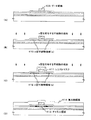
まず、第一の基板としてTFT形成基板101上に薄膜デバイスを作製する(薄膜デバイス102となる)。平坦化膜103をつけて、第二の基板との接着面を平坦にしておくとよい(図1(a))。
【0072】
第二の基板として支持材104を用意し、偏光フィルム107を接着剤で貼り付けておく。なおここでは、2種類の接着剤を使い分けて接着する例を示す。接着剤A105は、後述するように第一の基板と第二の基板を貼り合わせた際に薄膜デバイス102の外側となる部分を接着し、接着剤B106は粘着材で支持材104を取り除くまでの間、偏光フィルムを仮止めする(図1(b))。
【0073】
もちろん、TFT形成基板101上の平坦化膜103上に偏光フィルムを貼り付けて、支持材104と接着してもよい。
【0074】
図1(c)で、薄膜デバイス102を介してTFT形成基板101上部に形成した平坦化基板103の縁辺と、支持材104の偏光フィルム107を貼り付けた面の縁辺とに接着材を塗布して、両方の基板を接着する。そして、バックグラインドやCMP等で第一の基板を取り除き、薄膜デバイス102を表面に出す(図1(d))。実際には、薄膜デバイス102の最下層に窒化膜等を用意しておき、研磨工程の最後にウエットエッチングを行い、そのストッパーとして用いるとよい。
【0075】
次に、支持材104に保持された薄膜デバイス102に、画素電極108を形成する(図2(a))。偏光フィルム112に対向電極110をつけ、封止材111で液晶109を閉じこめる(図2(b))。なお、偏光フィルムがたわむ場合は、もう一つ別の支持材を用意して、偏光フィルム112を支えてもよい。
【0076】
図3(a)では、薄膜デバイス102の外側で接着剤A105を切り離せる場所で、基板を切断する。切断する事によって、接着剤A105が塗布された領域はなくなり、接着剤B106として粘着材が塗布された領域だけになるので(図3(b))、支持材104を取り除く(図3(c))。
【0077】
このように、基板に固定した状態で作製し、最終的には基板を取り除くことによって、半導体装置にフレキシビリティ(可撓性)をもたせ、薄型化、軽量化することができる。なお、ここではアクティブマトリクス型液晶表示装置に関して示したので、基板を取り除いた後の表面には偏光フィルムが貼られているが、使用目的に応じて、表面保護のためのフィルム、支持材としてのフィルム等を自由に組み合わせて、使うことができる。
【0078】
(実施の形態2)
本発明の作製方法を、薄膜トランジスタ(TFT)を用いた半導体装置について簡単に説明する。ここでは、薄膜トランジスタ1個分と配線の断面図を利用して話を進めるが、もちろん複数のトランジスタを用いた集積回路にも適用できる。
【0079】
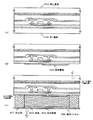
図4(A)で、第一基板1101上に、後で第一基板1101を取り除く際に利用するエッチングストッパー1102を形成し、その上に下部絶縁膜1103、シリコン等半導体からなる活性層1104、ゲート絶縁膜1105、ゲート電極1106を形成してトランジスタを構成する。第一層間絶縁膜1107を成膜し、活性層1104に到達する開孔部を形成し、開孔部を介して第一配線1108を形成する。第二層間絶縁膜1109を成膜する(図4(A))。
【0080】
第一基板1101上の薄膜デバイスを形成した面に第二基板1110を接着し、第一基板1101とエッチングストッパー1102を取り除き、活性層1104に到達する開孔部を形成する(図4(B))。エッチングストッパー1102は必ずしも必要なものではないが、トランジスタの最下層に窒化膜等を用意しておき、最後にウエットエッチングを行って、そのストッパーとして用いるとよい。
【0081】
そして、開孔部を介して活性層に接する第二配線1111を形成して、絶縁膜1112を形成する(図5(A))。今回は活性層を通して、第一配線1108と第二配線1111の導通をとったが、図5(B)のように、アライメント精度分だけ大きめの開孔部を設け、直接つないでもよい。どちらにしても本発明の構造では、上下から開孔部を設けるので、導通をとりやすい。また、活性層を形成した後で配線を形成するので、耐熱性の低い配線でも使える。
【0082】
図6に活性層、ゲート絶縁膜、ゲート電極、第一層間絶縁膜、第一配線、第二層間絶縁膜、第二配線、の従来構造の配線も、比較のために、同時に図示する。なお、第一配線1151、1154、第二配線1155、1157は、ここで図示されている薄膜トランジスタに電気的に接続されていない配線の断面である。
【0083】
もし本発明の構造を用いていなければ、第二配線1158は1156の場所になり、第二配線1156は第一配線1154と近く、寄生容量も大きくなる。また第二配線1157は1155の場所、もしくは第一配線として1151に形成してもよい。この場合も第一配線1152との距離が近くなってしまう。
【0084】
つまり、第一配線と第二配線の距離は、従来構造では第二層間絶縁膜の厚さであり、本発明の作製方法では、下部絶縁膜と第一層間絶縁膜を合わせた厚さになる。もちろん、第二層間絶縁膜の厚さより、下部絶縁膜と第一層間絶縁膜を合わせた厚さの方が大きくなる。
【0085】
このように、本発明の作製方法を用いれば、配線間の絶縁膜を実質的に厚くとることができ、異なる層に形成された配線間に生じる寄生容量を低減できる。なお、従来のように、ただ絶縁膜を厚くするのでは、絶縁膜を通しての導通のとりやすさに問題があったが、本発明の作製方法では問題ない。また、活性層の下部に配線を設けた従来構造と同じ構造であるが、活性層を形成後に配線を形成するので、耐熱性の低い配線材料も使うことができ、耐熱性が低いがために使えなかった低抵抗な配線を使うこともできる。
【0086】
【実施例】
[実施例1]
ここでは、本発明の半導体装置の作製方法を、アクティブマトリクス型液晶表示装置に適用する例を示す。なお図では、接着剤を使い分ける位置、封止材の位置、基板を切断する位置等を説明するため、液晶表示装置の一画素のみの断面を示すが、もちろん、複数の画素を有する液晶表示装置、駆動回路を一体形成した液晶表示装置等にも、本発明は適用できる。
【0087】
図7(A)において、第一基板400にはガラス基板や石英基板を使用することができる。その他にもシリコン基板、金属基板またはステンレス基板の表面に絶縁膜を形成したものを基板として用いてもよい。
【0088】
後で、第一基板400を取り除く時のために、エッチングストッパー401を形成する。エッチングストッパー401は、第一基板との選択比が十分なものを選ぶ。本実施例では、第一基板400に石英基板を使用し、エッチングストッパー401に窒化膜を10nm〜1000nm(代表的には100〜500nm)形成する。
【0089】
エッチングストッパー401上に第一絶縁膜402を、酸化シリコン膜で10〜1000nm(代表的には300〜500nm)の厚さに形成する。また、酸化窒化シリコン膜を用いてもよい。
【0090】
連続して、第一絶縁膜402上に、10〜100nmの非晶質半導体膜(本実施例では非晶質シリコン膜(アモルファスシリコン膜)403)を公知の成膜法で形成する(図7(B))。なお、非晶質半導体膜としては、非晶質シリコン膜以外にも、非晶質シリコンゲルマニウム膜などの非晶質の化合物半導体膜を用いることもできる。
【0091】
そして、特開平7−130652号公報(USP5,643,826号に対応)に記載された技術に従って結晶構造を含む半導体膜(本実施例では結晶質シリコン膜404)を形成する。同公報記載の技術は、非晶質シリコン膜の結晶化に際して、結晶化を助長する触媒元素(ニッケル、コバルト、ゲルマニウム、錫、鉛、パラジウム、鉄、銅から選ばれた一種または複数の元素、代表的にはニッケル)を用いる結晶化手段である。
【0092】
具体的には、非晶質シリコン膜表面に触媒元素を保持させた状態で加熱処理を行い、非晶質シリコン膜を結晶質シリコン膜に変化させるものである。本実施例では同公報の実施例1に記載された技術を用いるが、実施例2に記載された技術を用いてもよい。なお、結晶質シリコン膜にはいわゆる単結晶シリコン膜も多結晶シリコン膜も含まれるが、本実施例で形成される結晶質シリコン膜は結晶粒界を有するシリコン膜である。
【0093】
非晶質シリコン膜は含有水素量にもよるが、好ましくは400〜550℃で数時間加熱処理して脱水素処理を行い、含有水素量を5atomic%以下として結晶化の工程を行うことが望ましい。また、非晶質シリコン膜をスパッタ法や蒸着法などの他の作製法で形成してもよいが、膜中に含まれる酸素、窒素、などの不純物元素を十分に低減させておくことが望ましい。
【0094】
非晶質シリコン膜403に対して、公知の技術を使って結晶質シリコン膜(ポリシリコン膜または多結晶シリコン膜)404を形成する。本実施例では、非晶質シリコン膜403に対してレーザーから発する光(レーザー光)を照射して結晶質シリコン膜404を形成した(図7(C))。レーザーとしては、パルス発振型または連続発振型のエキシマレーザーを用いればよいが、連続発振型のアルゴンレーザーでもよい。または、Nd:YAGレーザーもしくはNd:YVOレーザーの第二高調波、第三高調波または第四高調波を用いてもよい。さらに、レーザー光のビーム形状は線状(長方形状も含む)であっても矩形状であってもかまわない。
【0095】
また、レーザー光のかわりにランプから発する光(ランプ光)を照射(以下、ランプアニールという)してもよい。ランプ光としては、ハロゲンランプ、赤外線ランプ等から発するランプ光を用いることができる。
【0096】
このようにレーザー光またはランプ光により熱処理(アニール)を施す工程を光アニール工程という。光アニール工程は短時間で高温熱処理が行えるため、ガラス基板等の耐熱性の低い基板を用いる場合にも効果的な熱処理工程を高いスループットで行うことができる。もちろん、目的はアニールであるので電熱炉を用いたファーネスアニール(熱アニールともいう)で代用することもできる。
【0097】
本実施例では、パルス発振型エキシマレーザー光を線状に加工してレーザーアニール工程を行う。レーザーアニール条件は、励起ガスとしてXeClガスを用い、処理温度を室温、パルス発振周波数を30Hzとし、レーザーエネルギー密度を250〜500mJ/cm2(代表的には350〜400mJ/cm2)とする。
【0098】
上記条件で行われるレーザーアニール工程は、熱結晶化後に残存した非晶質領域を完全に結晶化するとともに、既に結晶化された結晶質領域の欠陥等を低減する効果を有する。そのため、本工程は光アニールにより半導体膜の結晶性を改善する工程、または半導体膜の結晶化を助長する工程と呼ぶこともできる。このような効果はランプアニールの条件を最適化することによっても得ることが可能である。
【0099】
次に、結晶質シリコン膜404上に、後の不純物添加時のために保護膜405を形成する(図7(D))。保護膜405は100〜200nm(好ましくは130〜170nm)の厚さの窒化酸化シリコン膜または酸化シリコン膜を用いる。この保護膜405は不純物添加時に結晶質シリコン膜404が直接プラズマにさらされないようにするためと、微妙な温度制御を可能にするための意味がある。
【0100】
続いて、保護膜405を介してp型を付与する不純物元素(以下、p型不純物元素という)を添加する。p型不純物元素としては、代表的には周期表の13族に属する元素、典型的にはボロンまたはガリウムを用いることができる。この工程(チャネルドープ工程という)は、TFTしきい値電圧を制御するための工程である。なお、ここではジボラン(B2H6)を質量分離しないでプラズマ励起したイオンドープ法でボロンを添加した。もちろん、質量分離を行うイオンインプランテーション法を用いてもよい。
【0101】
この工程により1×10¹⁵〜1×10¹⁸atoms/cm3(代表的には5×1016〜5×1017atoms/cm3)の濃度で、p型不純物元素(本実施例ではボロン)を含むp型不純物領域(a)406を形成する(図7(D))。
【0102】
次に、保護膜405を除去した後、結晶質シリコン膜の不要な部分を除去して、島状の半導体膜(以下、活性層という)407を形成する(図7(E))。
【0103】
活性層407を覆って、ゲート絶縁膜408を形成する(図7(F))。ゲート絶縁膜408は、10〜200nm、好ましくは50〜150nmの厚さに形成すればよい。本実施例では、プラズマCVD法でN2OとSiH4を原料とした窒化酸化シリコン膜を80nm成膜する。
【0104】
図示しないが、ゲート配線409として、厚さ50nmの窒化タングステン(WN)と、厚さ350nmのタンタル(Ta)との2層の積層膜を形成する(図8(A))。ゲート配線は単層の導電膜で形成してもよいが、必要に応じて2層、3層といった積層膜とすることが好ましい。
【0105】
なお、ゲート配線としては、タンタル(Ta)、チタン(Ti)、モリブデン(Mo)、タングステン(W)、クロム(Cr)、シリコン(Si)から選ばれた元素、または前記元素を組み合わせた合金膜(代表的には、Mo−W合金、Mo−Ta合金)を用いることができる。
【0106】
次に、ゲート配線409をマスクとして自己整合的にn型不純物元素(本実施例ではリン)を添加する(図8(B))。こうして形成されたn型不純物領域(a)410には、前記のチャネルドープ工程で添加されたボロン濃度よりも5〜10倍高い濃度(代表的には1×10¹⁶〜5×10¹⁸atoms/cm3、典型的には3×1017〜3×1018atoms/cm3)でリンが添加されるように調整する。
【0107】
レジストマスク411を形成し、n型不純物元素(本実施例ではリン)を添加して、高濃度にリンを含むn型不純物領域(b)412を形成する(図8(C))。ここでも、フォスフィン(PH3)を用いたイオンドープ法(もちろん、イオンインプランテーション法でもよい)で行い、この領域のリンの濃度は1×10²⁰〜1×10²¹atoms/cm3(代表的には2×1020〜5×1020atoms/cm3)とする。
【0108】
また、n型不純物領域(b)412が形成された領域には、すでに前工程で添加されたリンまたはボロンが含まれるが、十分に高い濃度でリンが添加されることになるので、前工程で添加されたリンまたはボロンの影響は考えなくてよい。
【0109】
レジストマスク411を除去した後、第三絶縁膜414を形成する(図8(D))。第三絶縁膜414としては、シリコンを含む絶縁膜、具体的には窒化シリコン膜、酸化シリコン膜、窒化酸化シリコン膜、またはそれらを組み合わせた積層膜で、膜厚は600nm〜1.5μmとすればよい。本実施例では、プラズマCVD法でSiH4、N2O、NH3を原料ガスとし、1μm厚の窒化酸化シリコン膜(但し窒素濃度が25〜50atomic%)を用いる。
【0110】
その後、それぞれの濃度で添加されたn型またはp型不純物元素を活性化するために熱処理工程を行う(図8(D))。この工程はファーネスアニール法、レーザーアニール法、またはラピッドサーマルアニール(RTA)法で行うことができる。ここでは、ファーネスアニール法で活性化工程を行う。加熱処理は窒素雰囲気中において300〜650℃、好ましくは400〜550℃、ここでは550℃、4時間の熱処理を行う。
【0111】
この時、本実施例において、非晶質シリコン膜の結晶化に用いた触媒元素(本実施例ではニッケル)が、矢印で示す方向に移動して、前記の図8(C)の工程で形成された高濃度にリンを含むn型不純物領域(b)412に捕獲(ゲッタリング)される。これは、リンによる金属元素のゲッタリング効果に起因する現象であり、この結果、チャネル領域413は前記触媒元素の濃度が1×10¹⁷atoms/cm3以下(好ましくは1×1016atoms/cm3以下)となる。
【0112】
また逆に触媒元素のゲッタリングサイトとなった領域(図8(C)の工程で形成されたn型不純物領域(b)412)は高濃度に触媒元素が偏析して、5×10¹⁸atoms/cm3以上(代表的には1×1019〜5×1020atoms/cm3)の濃度で存在するようになる。
【0113】
さらに、3〜100%の水素を含む雰囲気中で、300〜450℃で1〜12時間の熱処理を行い、活性層を水素化する工程を行う。この工程は熱的に励起された水素により、半導体層のダングリングボンドを終端する工程である。水素化の他の手段として、プラズマ水素化(プラズマにより励起された水素を用いる)を行ってもよい。
【0114】
その後、TFTのソース・ドレイン領域に達する開孔部415(図9(A))、ソース・ドレイン配線416を形成する(図9(B))。また、図示していないが、本実施例ではこの配線は、Ti膜を100nm、Tiを含むアルミニウム膜を300nm、Ti膜150nmをスパッタ法で連続して形成した3層構造の積層膜である。
【0115】
次に、パッシベーション膜417として、窒化シリコン膜、酸化シリコン膜、または窒化酸化シリコン膜で50〜500nm(代表的には200〜300nm)の厚さで形成する(図9(C))。この時、本実施例では膜の形成に先立ってH2、NH3等水素を含むガスを用いてプラズマ処理を行い、成膜後に熱処理を行う。この前処理により励起された水素が第三絶縁膜414中に供給される。この状態で熱処理を行うことで、パッシベーション膜417の膜質を改善するとともに、第三絶縁膜414中に添加された水素が下方側に拡散するため、効果的に活性層を水素化することができる。
【0116】
また、パッシベーション膜417を形成した後に、さらに水素化工程を行ってもよい。例えば、3〜100%の水素を含む雰囲気中で、300〜450℃で1〜12時間の熱処理を行うとよい。あるいはプラズマ水素化法を用いても同様の効果が得られる。
【0117】
その後、平坦化膜として有機樹脂からなる第四絶縁膜418を約1μmの厚さに形成する(図9(C))。有機樹脂としては、ポリイミド、アクリル、ポリアミド、ポリイミドアミド、BCB(ベンゾシクロブテン)等を使用することができる。有機樹脂膜を用いることの利点は、成膜方法が簡単である点や、比誘電率が低いので、寄生容量を低減できる点、平坦性に優れる点などが上げられる。なお上述した以外の有機樹脂膜や有機系SiO化合物などを用いることもできる。
ここでは、基板に塗布後、熱重合するタイプのポリイミドを用い、300℃で焼成して形成する。
【0118】
次に、第二基板419を用意し、第二基板419を第一基板400にあわせた時に、薄膜デバイスが形成されていない領域に接着材420を塗布し、それ以外の領域には、偏光フィルム422が動かないように粘着材421を塗布しておく(図9(D))。
【0119】
ここで、第二基板419としては、ガラス基板や石英基板、その他にもシリコン基板、金属基板またはステンレス基板等が使える。また、接着材420は、後で切り落とす部分(薄膜デバイスが形成されていない領域)を接着するので、特に透明である必要もなく、耐熱性のあるものを選べばよい。例えば、一般に偏光フィルムの接着に用いられているポリビニルアルコール(PVA)系の接着材がある。粘着材421としては、耐熱性、透明性のよいものがよく、アクリル系、ウレタン系、シリコン系等の粘着材があげられる。
【0120】
図10(A)で、第一基板400のTFTを形成した面と、第二基板419の偏光フィルムを貼り付けた面とを接着する。接着材には、透明で耐熱性のあるもの、例えば、ポリビニルアルコール(PVA)系の接着材を使えばよい。
【0121】
そして、第二基板419に保持された状態で、第一基板400をバックグラインドやCMP等を使って削り落とす(図10(B))。本実施例では、第一基板400に石英基板、エッチングストッパー401に窒化膜を使用しているので、最後はフッ酸を使ったウエットエッチングに切り替える。なお、ウエットエッチングの際にパターニングして第一基板400の一部を残し、液晶表示装置のスペーサーとして用いることもできる。また、本実施例では窒化膜でできたエッチングストッパー401も、その後ドライエッチングにより取り除いている。
【0122】
次に、第一絶縁膜402に画素電極に導通をとるための開孔部を設け、画素電極423を形成する(図10(B))。画素電極423は、透過型液晶表示装置とする場合には透明導電膜を用い、反射型の液晶表示装置とする場合には金属膜を用いればよい。ここでは透過型の液晶表示装置とするために、酸化インジウム・スズ(ITO)膜を110nmの厚さにスパッタ法で形成する。
【0123】
また、画素電極に導通をとるための方法としては、図9(A)でTFTのソース・ドレイン領域に達する開孔部415を開けるときに、活性層のない部分にエッチングストッパー401に達する開孔部を開けておき、図9(B)のソース・ドレイン配線416で導通をとる方法もある。この方法を用いると、活性層のない部分で導通をとるため、画素の開口率が落ちるものの、画素電極423を平坦なものにすることができる。
【0124】
その後、図示していないが、ポリイミド膜を使って配向膜を形成し、ラビング処理を施して液晶分子がある一定のプレチルト角を持って配向するようにする。そして、偏光フィルム426に対向電極425を形成し、公知のセル組み工程によってシール材やスペーサ(共に図示せず)などを介して貼りあわせ、液晶424を封止材427を用いて封止する(図10(C))。なお、光の入射方向が、光1の場合には、偏光フィルム422上に遮光膜を形成することが好ましい。また、光の入射方向が光2の場合には、第1絶縁膜402の上または下に遮光膜となる膜を形成することが好ましい。液晶には公知の液晶材料を用いれば良い。なお、偏光フィルム426がたわむ場合は、第二基板419と同様の支持材をもう一つ用意してもよい。対向にある偏光フィルム426には、必要に応じてカラーフィルターや遮蔽膜を形成しても良い。
【0125】
次に、図11(A)に示すように、接着剤420で接着された部分を切断する。後は、粘着材421で止められた部分だけになるので、第二基板419をはがし、薄く、軽量でフレキシブルなアクティブマトリクス型液晶表示装置が完成する(図11(B))。
【0126】
さらに図12に、駆動回路を一体形成した液晶表示装置を、本発明の作製方法を用いて作製した例を示す。図12は、第一基板上に、ソース信号駆動回路1302、ゲート信号駆動回路1303、画素部1301を構成するトランジスタを形成し、第二基板に接着した後、第一基板を取り除き、液晶を封入したもの(1306:液晶封入領域)を、液晶側から見た図である。
【0127】
図12に示す液晶表示装置は、画素部1301と、ソース信号駆動回路1302、ゲート信号駆動回路1303とで構成される。画素部1301はnチャネル型TFTであり、周辺に設けられる駆動回路はCMOS回路を基本として構成されている。ソース信号駆動回路1302とゲート信号駆動回路1303は、接続配線1304を用いてFPC(フレキシブルプリントサーキット)1305に接続され、外部駆動回路から信号を受け取る。
【0128】
図13に、図12のA−A'で切断した断面図を示す。偏光フィルム1401、対向電極1402、封止剤1404、で囲まれた液晶1403が、画素TFT1406に接続された画素電極1405下にある。今回は、駆動TFT1407の下にも液晶1403があるが、寄生容量を減らしたい場合等には、画素電極1405下にのみ液晶1403を配置すればよい。駆動TFT1407には、導電性材料1408で接着されたFPC1409から信号が入力される。偏光フィルム1410を、液晶1403に対して、偏光フィルム1401と反対側に設けることで、透過型の表示装置として機能する。
【0129】
[実施例2]
本実施例では、本発明を用いて形成した薄膜デバイスを重ね合わせ、3次元実装する例を図を用いて簡単に説明する。
【0130】
図9(C)まで、実施例1と同様であるので説明を省略する。図14(A)は、図9(A)とほぼ同じ状態であるが、ソース・ドレイン配線416を延長して電極900を形成している。なお、説明のためにトランジスタを2個表示し、実施例1と共通な部分は同じ符号を用いている。
【0131】
ここで、開孔部901を開け、電極900と導通がとれるようにしておく(図14(B))。第二基板419には、実施例1と同様に接着剤420と粘着材421を塗るが、偏光フィルムは必要ない(図14(C))。偏光フィルムは必要ないが、剛性保持のための薄い板材や保護フィルム等を使用してもよい。この場合、薄い板材や保護フィルムには、開孔部901に対応する位置にあらかじめ、開孔部を設けておく。図15(A)で、第一基板400の薄膜デバイスを形成した面と第二基板419を、接着剤420と粘着材421を使って接着する。
【0132】
実施例1と同様、第一基板400とエッチングストッパー401を取り除く。第一絶縁膜402に開孔部を開け、電極(配線ともいう)902を形成する。電極902を覆って、パッシベーション膜903、第五絶縁膜904を形成し、電極902に導通がとれるように開孔部905を設けておく。パッシベーション膜903は実施例1のパッシベーション膜417と同様、窒化シリコン膜、酸化シリコン膜、または窒化酸化シリコン膜で50〜500nm(代表的には200〜300nm)の厚さで形成すればよい。第五絶縁膜904は実施例1の第四絶縁膜418と同様、平坦化や保護膜の意味がある。ここまでの工程で、図15(B)の状態になっている。
【0133】
そして、実施例1と同じ方法で第二基板419を取り除く。ここまでの工程でできる薄膜デバイスを複数作製し、導電性ペースト906で電極間に導通をとり、それらを接着剤で貼り合わせると、3次元実装された半導体装置ができあがる(図16)。近年、大容量化や小型化、軽量化が求められているメモリは、3次元実装の技術の実用化が注目されており、本発明を用いると、工程が複雑化することなく、簡便に3次元実装された半導体装置を実現することができる。なお図16では、貼り合わされた薄膜デバイスは、薄膜トランジスタのソース・ドレイン領域を介して導通をとっているように示されているが、配線同士の導通を直接とってもよい。
【0134】
[実施例3]
本実施例では、絶縁体上に形成した半導体薄膜を活性層に用いた薄膜トランジスタ(TFT)を用いた半導体装置について説明する。なお図では、配線と活性層、配線と絶縁膜等の位置関係を説明するため、薄膜トランジスタ一個分と配線の断面を示すが、もちろん、複数の薄膜トランジスタを有する集積回路にも本発明は適用できる。
【0135】
図17(A)において、第一基板2401にはガラス基板や石英基板を使用することができる。その他にもシリコン基板、金属基板またはステンレス基板の表面に絶縁膜を形成したものを基板として用いてもよい。
【0136】
後で、第一基板2401を取り除く時のために、エッチングストッパー2402を形成する。エッチングストッパー2402は、第一基板との選択比が十分なものを選ぶ。本実施例では、第一基板2401に石英基板を使用し、エッチングストッパー2402に窒化膜を10nm〜1000nm(代表的には100〜500nm)形成する。
【0137】
エッチングストッパー2402上に下部絶縁膜2403を、酸化シリコン膜で10〜1000nm(代表的には300〜500nm)の厚さに形成する。また、酸化窒化シリコン膜を用いてもよい。
【0138】
連続して、下部絶縁膜2403上に、10〜100nmの非晶質半導体膜(本実施例では非晶質シリコン膜(アモルファスシリコン膜)2404)を公知の成膜法で形成する(図17(B))。なお、非晶質半導体膜としては、非晶質シリコン膜以外にも、非晶質シリコンゲルマニウム膜などの非晶質の化合物半導体膜を用いることもできる。
【0139】
そして、特開平7−130652号公報(USP5,643,826号に対応)に記載された技術に従って結晶構造を含む半導体膜(本実施例では結晶質シリコン膜2405)を形成する。同公報記載の技術は、非晶質シリコン膜の結晶化に際して、結晶化を助長する触媒元素(ニッケル、コバルト、ゲルマニウム、錫、鉛、パラジウム、鉄、銅から選ばれた一種または複数の元素、代表的にはニッケル)を用いる結晶化手段である。
【0140】
具体的には、非晶質シリコン膜表面に触媒元素を保持させた状態で加熱処理を行い、非晶質シリコン膜を結晶質シリコン膜に変化させるものである。本実施例では同公報の実施例1に記載された技術を用いるが、実施例2に記載された技術を用いてもよい。なお、結晶質シリコン膜にはいわゆる単結晶シリコン膜も多結晶シリコン膜も含まれるが、本実施例で形成される結晶質シリコン膜は結晶粒界を有するシリコン膜である。
【0141】
非晶質シリコン膜は含有水素量にもよるが、好ましくは400〜550℃で数時間加熱処理して脱水素処理を行い、含有水素量を5atomic%以下として結晶化の工程を行うことが望ましい。また、非晶質シリコン膜をスパッタ法や蒸着法などの他の作製法で形成してもよいが、膜中に含まれる酸素、窒素、などの不純物元素を十分に低減させておくことが望ましい。
【0142】
非晶質シリコン膜2404に対して、公知の技術を使って結晶質シリコン膜(ポリシリコン膜または多結晶シリコン膜)2405を形成する。本実施例では、非晶質シリコン膜2404に対してレーザーから発する光(レーザー光)を照射して結晶質シリコン膜2405を形成した(図17(C))。レーザーとしては、パルス発振型または連続発振型のエキシマレーザーを用いればよいが、連続発振型のアルゴンレーザーでもよい。または、Nd:YAGレーザーもしくはNd:YVO4レーザーの第二高調波、第三高調波または第四高調波を用いてもよい。さらに、レーザー光のビーム形状は線状(長方形状も含む)であっても矩形状であってもかまわない。
【0143】
また、レーザー光のかわりにランプから発する光(ランプ光)を照射(以下、ランプアニールという)してもよい。ランプ光としては、ハロゲンランプ、赤外線ランプ等から発するランプ光を用いることができる。
【0144】
このようにレーザー光またはランプ光により熱処理(アニール)を施す工程を光アニール工程という。光アニール工程は短時間で高温熱処理が行えるため、ガラス基板等の耐熱性の低い基板を用いる場合にも効果的な熱処理工程を高いスループットで行うことができる。もちろん、目的はアニールであるので電熱炉を用いたファーネスアニール(熱アニールともいう)で代用することもできる。
【0145】
本実施例では、パルス発振型エキシマレーザー光を線状に加工してレーザーアニール工程を行う。レーザーアニール条件は、励起ガスとしてXeClガスを用い、処理温度を室温、パルス発振周波数を30Hzとし、レーザーエネルギー密度を250〜500mJ/cm2(代表的には350〜400mJ/cm2)とする。
【0146】
上記条件で行われるレーザーアニール工程は、熱結晶化後に残存した非晶質領域を完全に結晶化するとともに、既に結晶化された結晶質領域の欠陥等を低減する効果を有する。そのため、本工程は光アニールにより半導体膜の結晶性を改善する工程、または半導体膜の結晶化を助長する工程と呼ぶこともできる。このような効果はランプアニールの条件を最適化することによっても得ることが可能である。
【0147】
次に、結晶質シリコン膜2405上に、後の不純物添加時のために保護膜2406を形成する(図17(D))。保護膜2406は100〜200nm(好ましくは130〜170nm)の厚さの窒化酸化シリコン膜または酸化シリコン膜を用いる。この保護膜2406は不純物添加時に結晶質シリコン膜2405が直接プラズマにさらされないようにするためと、微妙な温度制御を可能にするための意味がある。
【0148】
続いて、保護膜2406を介してp型を付与する不純物元素(以下、p型不純物元素という)を添加する。p型不純物元素としては、代表的には周期表の13族に属する元素、典型的にはボロンまたはガリウムを用いることができる。この工程(チャネルドープ工程という)は、TFTしきい値電圧を制御するための工程である。なお、ここではジボラン(B2H6)を質量分離しないでプラズマ励起したイオンドープ法でボロンを添加した。もちろん、質量分離を行うイオンインプランテーション法を用いてもよい。
【0149】
この工程により1×10¹⁵〜1×10¹⁸atoms/cm3(代表的には5×1016〜5×1017atoms/cm3)の濃度で、p型不純物元素(本実施例ではボロン)を含むp型不純物領域(a)2407を形成する(図17(D))。
【0150】
次に、保護膜2406を除去した後、結晶質シリコン膜の不要な部分を除去して、島状の半導体膜(以下、活性層という)2408を形成する(図17(E))。
【0151】
活性層2408を覆って、ゲート絶縁膜2409を形成する(図18(A))。ゲート絶縁膜409は、10〜200nm、好ましくは50〜150nmの厚さに形成すればよい。本実施例では、プラズマCVD法でN2OとSiH4を原料とした窒化酸化シリコン膜を80nm成膜する。
【0152】
図示しないが、ゲート電極2410として、厚さ50nmの窒化タングステン(WN)と、厚さ350nmのタンタル(Ta)との2層の積層膜を形成する(図18(B))。ゲート電極は単層の導電膜で形成してもよいが、必要に応じて2層、3層といった積層膜とすることが好ましい。
【0153】
なお、ゲート電極としては、タンタル(Ta)、チタン(Ti)、モリブデン(Mo)、タングステン(W)、クロム(Cr)、シリコン(Si)から選ばれた元素、または前記元素を組み合わせた合金膜(代表的には、Mo−W合金、Mo−Ta合金)を用いることができる。
【0154】
次に、ゲート電極2410をマスクとして自己整合的にn型不純物元素(本実施例ではリン)を添加する(図18(C))。こうして形成されたn型不純物領域(a)2411には、前記のチャネルドープ工程で添加されたボロン濃度よりも5〜10倍高い濃度(代表的には1×10¹⁶〜5×10¹⁸atoms/cm3、典型的には3×1017〜3×1018atoms/cm3)でリンが添加されるように調整する。
【0155】
レジストマスク2412を形成し、n型不純物元素(本実施例ではリン)を添加して、高濃度にリンを含むn型不純物領域(b)2413を形成する(図18(D))。ここでも、フォスフィン(PH3)を用いたイオンドープ法(もちろん、イオンインプランテーション法でもよい)で行い、この領域のリンの濃度は1×10²⁰〜1×10²¹atoms/cm3(代表的には2×1020〜5×1020atoms/cm3)とする。
【0156】
また、n型不純物領域(b)2413が形成された領域には、すでに前工程で添加されたリンまたはボロンが含まれるが、十分に高い濃度でリンが添加されることになるので、前工程で添加されたリンまたはボロンの影響は考えなくてよい。
【0157】
レジストマスク2412を除去した後、第一層間絶縁膜2414を形成する(図19(A))。第一層間絶縁膜2414としては、シリコンを含む絶縁膜、具体的には窒化シリコン膜、酸化シリコン膜、窒化酸化シリコン膜、またはそれらを組み合わせた積層膜で、膜厚は600nm〜1.5μmとすればよい。本実施例では、プラズマCVD法でSiH4、N2O、NH3を原料ガスとし、1μm厚の窒化酸化シリコン膜(但し窒素濃度が25〜50atomic%)を用いる。
【0158】
その後、それぞれの濃度で添加されたn型またはp型不純物元素を活性化するために熱処理工程を行う(図19(A))。この工程はファーネスアニール法、レーザーアニール法、またはラピッドサーマルアニール(RTA)法で行うことができる。ここでは、ファーネスアニール法で活性化工程を行う。加熱処理は窒素雰囲気中において300〜650℃、好ましくは400〜550℃、ここでは550℃、4時間の熱処理を行う。
【0159】
この時、本実施例において、非晶質シリコン膜の結晶化に用いた触媒元素(本実施例ではニッケル)が、矢印で示す方向に移動して、前記の図18(D)の工程で形成された高濃度にリンを含むn型不純物領域(b)2413に捕獲(ゲッタリング)される。これは、リンによる金属元素のゲッタリング効果に起因する現象であり、この結果、チャネル領域2415は前記触媒元素の濃度が1×10¹⁷atoms/cm3以下(好ましくは1×1016atoms/cm3以下)となる。
【0160】
また逆に触媒元素のゲッタリングサイトとなった領域(図18(D)の工程で形成されたn型不純物領域(b)2413)は高濃度に触媒元素が偏析して、5×10¹⁸atoms/cm3以上(代表的には1×1019〜5×1020atoms/cm3)の濃度で存在するようになる。
【0161】
さらに、3〜100%の水素を含む雰囲気中で、300〜450℃で1〜12時間の熱処理を行い、活性層を水素化する工程を行う。この工程は熱的に励起された水素により、半導体層のダングリングボンドを終端する工程である。水素化の他の手段として、プラズマ水素化(プラズマにより励起された水素を用いる)を行ってもよい。
【0162】
その後、TFTのソース・ドレイン領域に達する開孔部2416(図19(B))、第一配線2417を形成する(図19(C))。また、図示していないが、本実施例ではこの第一配線を、Ti膜を100nm、Tiを含むアルミニウム膜を300nm、Ti膜150nmをスパッタ法で連続して形成した3層構造の積層膜とする。
【0163】
次に、パッシベーション膜2418として、窒化シリコン膜、酸化シリコン膜、または窒化酸化シリコン膜で50〜500nm(代表的には200〜300nm)の厚さで形成する(図19(D))。この時、本実施例では膜の形成に先立ってH2、NH3等水素を含むガスを用いてプラズマ処理を行い、成膜後に熱処理を行う。この前処理により励起された水素が第一層間絶縁膜2414中に供給される。この状態で熱処理を行うことで、パッシベーション膜2418の膜質を改善するとともに、第一層間絶縁膜2414中に添加された水素が下方側に拡散するため、効果的に活性層を水素化することができる。
【0164】
また、パッシベーション膜2418を形成した後に、さらに水素化工程を行ってもよい。例えば、3〜100%の水素を含む雰囲気中で、300〜450℃で1〜12時間の熱処理を行うとよい。あるいはプラズマ水素化法を用いても同様の効果が得られる。
【0165】
その後、平坦化膜として有機樹脂からなる絶縁膜2419を約1μmの厚さに形成する(図19(D))。有機樹脂としては、ポリイミド、アクリル、ポリアミド、ポリイミドアミド、BCB(ベンゾシクロブテン)等を使用することができる。有機樹脂膜を用いることの利点は、成膜方法が簡単である点や、比誘電率が低いので、寄生容量を低減できる点、平坦性に優れる点などが上げられる。なお上述した以外の有機樹脂膜や有機系SiO化合物などを用いることもできる。ここでは、基板に塗布後、熱重合するタイプのポリイミドを用い、300℃で焼成して形成する。
【0166】
次に、第二基板2420を用意し、第一基板2401の薄膜デバイスを形成した面と第二基板を接着する(図20(A))。ここで、第二基板2420としては、ガラス基板や石英基板、その他にもシリコン基板、金属基板またはステンレス基板等が使える。本実施例では、第二基板2420として石英基板を用いる。この場合、接着剤には、エポキシ系やシアノアクリレート系、または光線硬化型接着剤等が使える。
【0167】
そして、第二基板2420に保持された状態で、第一基板2401をバックグラインドやCMP(Chemical Mechanical Polishing)等を使って削り落とす(図20(B))。本実施例では、第一基板2401に石英基板、エッチングストッパー2402に窒化膜を使用しているので、適当な厚さまで削った後、フッ酸を使ったウエットエッチングに切り替える。また、本実施例では窒化膜でできたエッチングストッパー2402も、その後ドライエッチングにより取り除いている。
【0168】
次に、下部絶縁膜2403に活性層2408に達する開孔部2421を設け(図20(B))、第二配線2422、絶縁膜2423を形成する(図20(C))。ここで、第二配線2422としては、すでに活性層2408の熱処理等が済んでいるので、耐熱性の低い配線材料でも使うことができる。第一配線2417と同様にアルミニウムを使ってもよいし、実施例4で示すように透過型液晶表示装置として使う場合には、酸化インジウム・スズ(ITO)を使ってもよい。
【0169】
このように、本発明の作製方法を用いれば、第一配線2417と第二配線2422の間の絶縁膜を厚くとることができ、寄生容量を低減できる。絶縁膜を通しての導通のとりやすさにも問題なく、また、耐熱性の低い配線材料も使うことができ、電気回路の高速動作や電気信号の正確な伝播に寄与することができる。
【0170】
[実施例4]
本実施例では、実施例3で作製した半導体装置から、アクティブマトリクス型液晶表示装置を作製する工程を説明する。図21に示すように、図20(B)の状態の基板に対し、第二配線2422を形成する。第二配線2422は、透過型液晶表示装置とする場合には透明導電膜を用い、反射型の液晶表示装置とする場合には金属膜を用いればよい。ここでは透過型の液晶表示装置とするために、酸化インジウム・スズ(ITO)膜を110nmの厚さにスパッタ法で形成する。
【0171】
そして、配向膜801を形成する。本実施例では配向膜としてポリイミド膜を用いた。また、対向基板805には、透明導電膜で対向電極804を、そして配向膜803を形成する。なお、対向基板には必要に応じてカラーフィルターや遮蔽膜を形成しても良い。
【0172】
配向膜803を形成した後、ラビング処理を施して液晶分子がある一定のプレチルト角を持って配向するようにする。そして、画素部と駆動回路が形成されたアクティブマトリクス基板(実施例3で作製した半導体装置)と対向基板とを、公知のセル組み工程によってシール材やスペーサ(共に図示せず)などを介して貼りあわせる。その後、両基板の間に液晶802を注入し、封止剤(図示せず)によって完全に封止する。液晶には公知の液晶材料を用いれば良い。このようにして図21に示すアクティブマトリクス型液晶表示装置が完成する。
【0173】
次に、このアクティブマトリクス型液晶表示装置を、駆動回路を一体形成した場合の全体構成を、図22に示す。尚、図23は、図22のA−A’ で切断した断面図である。図22は、第一基板上に、ソース信号駆動回路1902、ゲート信号駆動回路1903、画素部1901を構成するトランジスタを形成し、第二基板に接着した後、第一基板を取り除き、液晶を封入したもの(1906:液晶封入領域)を、液晶側から見た図である。
【0174】
図22に示す液晶表示装置は、画素部1901と、ソース信号駆動回路1902、ゲート信号駆動回路1903とで構成される。画素部1901はnチャネル型TFTであり、周辺に設けられる駆動回路はCMOS回路を基本として構成されている。ソース信号駆動回路1902とゲート信号駆動回路1903は、接続配線1904を用いてFPC(フレキシブルプリントサーキット)1905に接続され、外部駆動回路から信号を受け取る。
【0175】
図23は、対向電極1001、封止剤1003、で囲まれた液晶1002が、画素TFT1005に接続された画素電極1004の下にある。今回は、駆動TFT1006の下にも液晶1002があるが、寄生容量を減らしたい場合等には、画素電極1004下にのみ液晶1002を配置すればよい。駆動TFT1006には、導電性材料1007で接着されたFPC1008から信号が入力される。
【0176】
[実施例5]
本発明の半導体装置の作製方法を、アクティブマトリクス型EL(エレクトロルミネセンス)表示装置に適用する例を示す。
【0177】
実施例1の図10(B)まで同じであるが、偏光フィルム422は必要ない(図24(A))。画素電極1200としては、仕事関数の大きい透明導電膜が用いられる。透明導電膜としては、酸化インジウムと酸化スズとの化合物または酸化インジウムと酸化亜鉛との化合物を用いることができる。
【0178】
そして、画素電極1200の上(図では下)には第五絶縁膜1202が形成され、第五絶縁膜1202は画素電極1200の上に開孔部が形成されている。この開孔部において、画素電極1200の上にはEL層1201が形成される。EL層1201は公知の有機EL材料または無機EL材料を用いることができる。また、有機EL材料には低分子系(モノマー系)材料と高分子系(ポリマー系)材料があるがどちらを用いても良い。
【0179】
EL層1201の形成方法は公知の技術を用いれば良い。また、EL層の構造は正孔注入層、正孔輸送層、発光層、電子輸送層または電子注入層を自由に組み合わせて積層構造または単層構造とすれば良い。
【0180】
EL層1201の上(図では下)には遮光性を有する導電膜(代表的にはアルミニウム、銅もしくは銀を主成分とする導電膜またはそれらと他の導電膜との積層膜)からなる陰極1203が形成される。また、陰極1203とEL層1201の界面に存在する水分や酸素は極力排除しておくことが望ましい。従って、真空中で両者を連続成膜するか、EL層1201を窒素または希ガス雰囲気で形成し、酸素や水分に触れさせないまま陰極1203を形成するといった工夫が必要である。本実施例ではマルチチャンバー方式(クラスターツール方式)の成膜装置を用いることで上述のような成膜を可能とする。
【0181】
以上のようにして、画素電極1200、EL層1201及び陰極1203からなるEL素子が形成され、充填材1204により封入されている(図24(B))。
【0182】
カバー材1205としては、ガラス板、金属板(代表的にはステンレス板)、セラミックス板、FRP(Fiberglass Reinforced Plastics)板、PVF(ポリビニルフルオライド)フィルム、マイラーフィルム、ポリエステルフィルムまたはアクリルフィルムを用いることができる。また、アルミニウムホイルをPVFフィルムやマイラーフィルムで挟んだ構造のシートを用いることもできる。
【0183】
但し、EL素子からの光の放射方向がカバー材側に向かう場合にはカバー材は透明でなければならない。その場合には、ガラス板、プラスチック板、ポリエステルフィルムまたはアクリルフィルムのような透明物質を用いる。
【0184】
また、充填材1204としては紫外線硬化樹脂または熱硬化樹脂を用いることができ、PVC(ポリビニルクロライド)、アクリル、ポリイミド、エポキシ樹脂、シリコーン樹脂、PVB(ポリビニルブチラル)またはEVA(エチレンビニルアセテート)を用いることができる。この充填材1204の内部に吸湿性物質(好ましくは酸化バリウム)を設けておくとEL素子の劣化を抑制できる。
【0185】
また、充填材1204の中にスペーサを含有させてもよい。このとき、スペーサを酸化バリウムで形成すればスペーサ自体に吸湿性をもたせることが可能である。また、スペーサを設けた場合、スペーサからの圧力を緩和するバッファ層として陰極1203上に樹脂膜を設けることも有効である。
【0186】
最後に、実施例1と同様に基板を切断して、第二基板419を取り除く。こうして、薄くて軽い、アクティブマトリクス型EL表示装置が作製できる(図24(C))。
【0187】
[実施例6]
本実施例では、本発明を用いてEL(エレクトロルミネセンス)表示装置を作製した他の例について説明する。なお、図25は、第一基板上に、ソース信号駆動回路2102、ゲート信号駆動回路2103、画素部2101を構成するトランジスタを形成し、第二基板に接着した後、第一基板を取り除き、EL層を形成したものを、EL層側から見た図である。図26は、図11をA−A’ で切断した断面図である。
【0188】
図25、26において、2201は基板、2101は画素部、2102はソース信号駆動回路、2103はゲート信号駆動回路であり、それぞれの駆動回路は接続配線2104を経てFPC(フレキシブルプリントサーキット)2105に至り、外部機器へと接続される。
【0189】
このとき、画素部2101、ソース信号駆動回路2102及びゲート信号駆動回路2103を囲むようにして第1シール材2106、カバー材2107、充填材2208及び第2シール材2108が設けられている。
【0190】
図26は、図25をA−A’ で切断した断面図に相当し、基板2201の上にソース信号駆動回路2102に含まれる駆動TFT(但し、ここではnチャネル型TFTとpチャネル型TFTを図示している)2202及び画素部2101に含まれる画素TFT(但し、ここではEL素子への電流を制御するTFTを図示している)2203が形成されている。
【0191】
そして、画素電極2204は画素TFT2203のソース・ドレイン領域の一方と電気的に接続をとるように形成される。画素電極2204としては仕事関数の大きい透明導電膜が用いられる。透明導電膜としては、酸化インジウムと酸化スズとの化合物または酸化インジウムと酸化亜鉛との化合物を用いることができる。
【0192】
画素電極2204の上(図では下)には絶縁膜2205が形成され、絶縁膜2205は画素電極2204の上に開孔部が形成されている。この開孔部において、画素電極2204の上にはEL層2206が形成される。EL層2206は公知の有機EL材料または無機EL材料を用いることができる。また、有機EL材料には低分子系(モノマー系)材料と高分子系(ポリマー系)材料があるがどちらを用いても良い。
【0193】
EL層2206の形成方法は公知の技術を用いれば良い。また、EL層の構造は正孔注入層、正孔輸送層、発光層、電子輸送層または電子注入層を自由に組み合わせて積層構造または単層構造とすれば良い。
【0194】
EL層2206の上には遮光性を有する導電膜(代表的にはアルミニウム、銅もしくは銀を主成分とする導電膜またはそれらと他の導電膜との積層膜)からなる陰極2207が形成される。また、陰極2207とEL層2206の界面に存在する水分や酸素は極力排除しておくことが望ましい。従って、真空中で両者を連続成膜するか、EL層2206を窒素または希ガス雰囲気で形成し、酸素や水分に触れさせないまま陰極2207を形成するといった工夫が必要である。本実施例ではマルチチャンバー方式(クラスターツール方式)の成膜装置を用いることで上述のような成膜を可能とする。
【0195】
以上のようにして、画素電極2204、EL層2206及び陰極2207からなるEL素子が形成される。このEL素子は、第1シール材2106及び第2シール材2108によって基板2201に貼り合わされたカバー材2107で囲まれ、充填材2208により封入されている。
【0196】
カバー材2107としては、ガラス板、金属板(代表的にはステンレス板)、セラミックス板、FRP(Fiberglass Reinforced Plastics)板、PVF(ポリビニルフルオライド)フィルム、マイラーフィルム、ポリエステルフィルムまたはアクリルフィルムを用いることができる。また、アルミニウムホイルをPVFフィルムやマイラーフィルムで挟んだ構造のシートを用いることもできる。
【0197】
但し、EL素子からの光の放射方向がカバー材側に向かう場合にはカバー材は透明でなければならない。その場合には、ガラス板、プラスチック板、ポリエステルフィルムまたはアクリルフィルムのような透明物質を用いる。
【0198】
また、充填材2208としては紫外線硬化樹脂または熱硬化樹脂を用いることができ、PVC(ポリビニルクロライド)、アクリル、ポリイミド、エポキシ樹脂、シリコーン樹脂、PVB(ポリビニルブチラル)またはEVA(エチレンビニルアセテート)を用いることができる。この充填材2208の内部に吸湿性物質(好ましくは酸化バリウム)を設けておくとEL素子の劣化を抑制できる。
【0199】
また、充填材2208の中にスペーサを含有させてもよい。このとき、スペーサを酸化バリウムで形成すればスペーサ自体に吸湿性をもたせることが可能である。また、スペーサを設けた場合、スペーサからの圧力を緩和するバッファ層として陰極2207上に樹脂膜を設けることも有効である。
【0200】
また、接続配線2104は導電性材料2209を介してFPC2105に電気的に接続される。接続配線2104は画素部2101、ソース信号駆動回路2102及びゲート信号駆動回路2103に送られる信号をFPC2105に伝え、FPC2105により外部機器と電気的に接続される。
【0201】
また、本実施例では第1シール材2106の露呈部及びFPC2105の一部を覆うように第2シール材2108を設け、EL素子を徹底的に外気から遮断する構造となっている。こうして図26の断面構造を有するEL表示装置となる。
【0202】
[実施例7]
ここで、本発明の作製方法を用いて、ボトムゲート型薄膜トランジスタを形成する方法を簡単に説明する。図27に、そのトランジスタ1個分の断面図を示すが、作製方法は実施例3と基本的に同様である。なお、本明細書において、ボトムゲート型薄膜トランジスタとは、図27に示すような、ゲート電極と第二配線との間の層に活性層が形成されている(ゲート電極と配線とが、活性層の同一側には形成されていない)形状の薄膜トランジスタを指すこととする。
【0203】
実施例1と同様に図18(C)では、ゲート電極2410をマスクとして、セルフアラインで活性層2408に不純物を添加する。第一配線2417は必要ないので、ゲート電極2410の上にはパッシベーション膜2418、絶縁膜2419を形成して平坦化する。その後、第二基板2420を接着して、第一基板2401を取り除き、第二配線2422(なお、本実施例では第一配線は存在しないが、実施例3とそろえるために第二配線と表記している)、絶縁膜2423を形成する。
【0204】
このようにして、活性層に対して配線と反対側にゲート電極を持つボトムゲート型トランジスタが形成できるが、従来のボトムゲート型トランジスタとの違いは、セルフアラインで不純物を添加できるという点である。
【0205】
[実施例8]
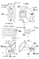
本発明のアクティブマトリクス型表示装置は電気器具の表示部として用いることができる。そのような電気器具としては、ビデオカメラ、デジタルカメラ、プロジェクター、プロジェクションTV、ゴーグル型ディスプレイ(ヘッドマウントディスプレイ)、ナビゲーションシステム、音響再生装置、ノート型パーソナルコンピュータ、ゲーム機器、携帯情報端末(モバイルコンピュータ、携帯電話、携帯型ゲーム機または電子書籍等)、記録媒体を備えた画像再生装置などが挙げられる。それら電気器具の具体例を図28に示す。
【0206】
図28(A)は携帯電話であり、本体3001、音声出力部3002、音声入力部3003、表示部3004、操作スイッチ3005、アンテナ3006で構成される。本発明のアクティブマトリクス型表示装置は表示部3004に用いることができる。
【0207】
図28(B)はビデオカメラであり、本体3101、表示部3102、音声入力部3103、操作スイッチ3104、バッテリー3105、受像部3106で構成される。本発明のアクティブマトリクス型表示装置は表示部3102に用いることができる。
【0208】
図28(C)はモバイルコンピュータ(モービルコンピュータ)であり、本体3201、カメラ部3202、受像部3203、操作スイッチ3204、表示部3205で構成される。本発明のアクティブマトリクス型表示装置は表示部3205に用いることができる。
【0209】
図28(D)はゴーグル型ディスプレイであり、本体3301、表示部3302、アーム部3303で構成される。本発明のアクティブマトリクス型表示装置は表示部3302に用いることができる。
【0210】
図28(E)はリアプロジェクター(プロジェクションTV)であり、本体3401、光源3402、液晶表示装置3403、偏光ビームスプリッタ3404、リフレクター3405、3406、スクリーン3407で構成される。本発明は液晶表示装置3403に用いることができる。
【0211】
図28(F)はフロントプロジェクターであり、本体3501、光源3502、液晶表示装置3503、光学系3504、スクリーン3505で構成される。本発明は液晶表示装置3503に用いることができる。
【0212】
以上の様に、本発明の適用範囲は極めて広く、あらゆる分野の電気器具に適用することが可能である。
【0213】
【発明の効果】
本発明は、半導体装置を薄型化、軽量化し、フレキシビリティを与えるものである。一般に基板を薄くすれば、半導体装置の作製工程が困難なものとなるが、本発明では、作製工程中のみ適当な支持材を用いて作製しやすくしている。本発明は、SOI構造の集積回路、アクティブマトリクス型液晶表示装置、アクティブマトリクス型EL表示装置など、絶縁体上に形成された半導体装置に適用可能である。
【0214】
また、本発明を用いれば、配線間の絶縁膜を厚くとることができ、異なる層に形成された配線間に生じる寄生容量を低減できる。さらに、従来構造において絶縁膜を厚く形成した時の、絶縁膜に開孔部を設けて導通をとる問題や、配線材料の耐熱性の問題を解決している。
【図面の簡単な説明】
【図1】 本発明の実施の形態を示す図。
【図2】 本発明の実施の形態を示す図。
【図3】 本発明の実施の形態を示す図。
【図4】 本発明の実施の形態を示す図。
【図5】 本発明の実施の形態を示す図。
【図6】 本発明の実施の形態を示す図。
【図7】 本発明の実施の一例を示す図。
【図8】 本発明の実施の一例を示す図。
【図9】 本発明の実施の一例を示す図。
【図10】 本発明の実施の一例を示す図。
【図11】 本発明の実施の一例を示す図。
【図12】 本発明の実施の一例を示す図。
【図13】 本発明の実施の一例を示す図。
【図14】 本発明の実施の一例を示す図。
【図15】 本発明の実施の一例を示す図。
【図16】 本発明の実施の一例を示す図。
【図17】 本発明の実施の一例を示す図。
【図18】 本発明の実施の一例を示す図。
【図19】 本発明の実施の一例を示す図。
【図20】 本発明の実施の一例を示す図。
【図21】 本発明の実施の一例を示す図。
【図22】 本発明の実施の一例を示す図。
【図23】 本発明の実施の一例を示す図。
【図24】 本発明を用いて作製されたアクティブマトリクス型EL表示装置を示す図。
【図25】 本発明を用いて作製されたアクティブマトリクス型EL表示装置を示す図。
【図26】 本発明を用いて作製されたアクティブマトリクス型EL表示装置を示す図。
【図27】 本発明の実施の一例を示す図。
【図28】 電気器具の一例を示す図。[0001]
BACKGROUND OF THE INVENTION
The present invention relates to a method for manufacturing a semiconductor device, and more particularly, to a method for manufacturing a thin and flexible semiconductor device. The present invention also relates to a method for reducing parasitic capacitance generated between wirings formed in different layers with an insulating film interposed therebetween. Note that in this specification, a semiconductor device refers to all devices that function by utilizing semiconductor characteristics, and in particular, the present invention uses an SOI (Silicon On Insulator) element in which a semiconductor layer is formed over an insulator. The present invention can be suitably applied to an integrated circuit, an active matrix type liquid crystal display device configured using thin film transistors (TFTs), an active matrix type EL display device, and the like. Here, in this specification, a thin film device refers to an electronic device including at least one of a thin film transistor (TFT) configured using a semiconductor thin film and a wiring, a conductive layer, a resistor, a capacitor, or the like.
[0002]
[Prior art]
As one of semiconductor devices, there is an integrated circuit using an SOI structure element in which a semiconductor layer is formed over an insulator. Since the semiconductor layer is formed over the insulator, parasitic capacitance is small and high-speed operation is possible.
[0003]
As one of semiconductor devices, there is an active matrix liquid crystal display device. In an active matrix liquid crystal display device, a substrate on which a thin film transistor (TFT) used as a pixel switching element (TFT) is formed and a substrate on which a counter electrode is formed (opposite substrate) are bonded together, and liquid crystal is injected into the gap. This structure is mainstream. In this active matrix liquid crystal display device, the voltage applied to the liquid crystal can be controlled for each pixel by a TFT formed on a transparent substrate such as glass, so that the image is clear and widely used in OA devices, TVs and the like. It has been.
[0004]
As one of semiconductor devices, an active matrix EL display device is known. An active matrix EL display device has a structure in which an EL material is sandwiched between two electrodes, and emits light by passing an electric current. Since the current flowing through the EL material can be controlled for each pixel by using a plurality of pixel transistors, the image is clear.
[0005]
These semiconductor devices are increasingly miniaturized and the degree of integration is improved. The parasitic capacitance generated between the wirings of the semiconductor device causes a propagation delay in the electric signal, and prevents high-speed operation of the electric circuit and accurate propagation of the electric signal. Parasitic capacitance generated between wirings may be generated between wirings formed in the same layer, or may be generated between wirings formed in different layers via an insulating film.
[0006]
When the degree of integration is improved, the distance between wirings formed in the same layer is reduced and the parasitic capacitance is increased. In order to reduce the parasitic capacitance between wirings formed in the same layer, the wirings may be moved to different layers. That is, the integration of wirings of the same layer is reduced by forming a multilayer wiring. Then, reducing the parasitic capacitance generated between the wirings formed in different layers via the insulating film contributes to the improvement of the integration degree of the entire semiconductor device.
[0007]
Therefore, in order to reduce the parasitic capacitance generated between the wirings formed in different layers via the insulating film, the insulating film is made thicker to increase the distance between the wirings, the insulating film having a low dielectric constant is used, etc. The method has been taken. However, when the insulating film is thickened, not only does it become difficult to open a hole in the insulating film in order to establish conduction between the wirings, for example, a conductive layer formed by sputtering breaks inside the hole, or Since a sufficient film thickness cannot be secured, problems such as increased resistance may occur. In addition, an insulating film having a low dielectric constant may cause problems related to film quality such as heat resistance and water permeability and processing problems such as dimensional change due to etching. For example, in the case of acrylic having a thickness of 1 μm, although depending on the etching conditions, the hole diameter may increase by about 1 μm, which may be an obstacle to improving the integration degree of the entire semiconductor device.
[0008]
There is also a method of changing the formation order of the conductive layers for forming the wiring. Here, in the case where an integrated circuit having two layers of wirings for conducting between elements is constituted by a top gate transistor, the following arrangement is usually given in the order of film formation. Active layer, first insulating film (gate insulating film), first conductive layer (gate electrode), second insulating film (first interlayer insulating film), second conductive layer (first wiring), first Third insulating film (second interlayer insulating film), third conductive layer (second wiring).
[0009]
In other words, the first conductive layer (second wiring), the first insulating film (lower insulating film), the active layer, the second insulating film (gate insulating film), the second conductive layer (gate electrode) When the third insulating film (first interlayer insulating film) and the third conductive layer (first wiring) are configured, the distance between the first wiring and the second wiring is increased and formed therebetween. Parasitic capacitance can be reduced.
[0010]
In this case, although the distance between the first wiring and the second wiring is increased, for example, the problem of opening and conduction can be avoided through the active layer. However, even in the latter case, it is necessary to use the same second wiring that can withstand the film formation temperature of the active layer to be formed later and the thermal activation temperature of the implanted impurity. The same material cannot always be used. For example, Al is often used as a wiring material having a low resistivity, but cannot be used in the latter case because of its low heat resistance.
[0011]
In this specification, “electrode” is a part of “wiring”, and for convenience of explanation, “wiring” and “electrode” are used separately, but “wiring” is always included in the word “electrode”. It shall be.
[0012]
[Problems to be solved by the invention]
In recent years, semiconductor devices such as those described above are used in portable devices and the like, and are required to be thin, light, and flexible (flexible). Most of the thickness of the semiconductor device is the thickness of the substrate. To reduce the thickness and weight, the substrate may be made thinner. However, if the substrate is made thin, the substrate is warped during fabrication, causing troubles in the photoengraving process, and it is difficult to fabricate the substrate because the substrate is easily cracked during substrate transport. Therefore, if a semiconductor device can be manufactured on a transparent plastic substrate or the like, a light and flexible display device can be manufactured. However, this has not been realized yet due to problems such as heat resistance of the plastic substrate.
[0013]
In addition, high-speed operation of electric circuits and electric signals can be used to reduce the parasitic capacitance generated between wirings formed in different layers via insulating films, and to use wiring materials that were not usable due to low heat resistance such as Al. Enable accurate propagation.
[0014]
[Means for Solving the Problems]
Therefore, the present inventor has considered a method of fabricating a thin film device on a substrate having sufficient heat resistance and strength at the time of fabrication and removing the substrate. First, a thin film device is formed on a first substrate and bonded to a second substrate. In this state, a thin film device exists between the first substrate and the second substrate. Then, in a state where it is held on the second substrate, the first substrate is removed leaving the thin film device, and an opening reaching the thin film device held on the second substrate is provided, through the opening. Then, after performing necessary processing such as forming a conductive layer in contact with the thin film device, the second substrate is also removed.
[0015]
Furthermore, the present invention is characterized in that the first substrate and the second substrate are bonded to each other by applying an adhesive to a part of the region where the thin film device is not formed. Alternatively, an adhesive is applied to a part of the region where the thin film device is not formed, and the other part is temporarily fixed using an adhesive or the like. By doing so, the second substrate can be easily removed by cutting off the bonded portion.
[0016]
When the above manufacturing method is used, it is always held on one of the substrates at the time of manufacturing, but since both substrates are finally peeled off, the first substrate and the second substrate may be thick and sufficient. A strong substrate can be used. Therefore, the substrate is less likely to be warped and the substrate is not easily cracked, and the manufacturing is easy.
[0017]
Further, in display devices such as active matrix liquid crystal display devices and active matrix EL display devices, scratches on the back surface of the substrate when the substrate is transported cause a deterioration in display quality, which is a problem. When the manufacturing method is used, the substrate that was supported at the time of manufacturing is removed, so that this problem is also solved.
[0018]
Furthermore, if the said manufacturing method is used, an output electrode can be formed in the front and back both surfaces of a thin film device. Overlaying them can also be used for applications such as 3D mounting.
[0019]
In another aspect of the invention, an active layer, a first insulating film (gate insulating film), a first conductive layer (gate electrode), a second insulating film (first interlayer insulating film), a second conductive layer ( The first wiring) is formed in this order, and then the second wiring is formed on the side opposite to the first wiring with respect to the active layer. That is, the first conductive layer (second wiring), the first insulating film (lower insulating film), the active layer, the second insulating film (gate insulating film), the second conductive layer (gate electrode), the third This structure is intended to realize the structure of the first insulating film (first interlayer insulating film) and the third conductive layer (first wiring). Note that in this specification, an active layer refers to a layer formed of a semiconductor film including a channel region, a source region, and a drain region.
[0020]
Then, the parasitic capacitance formed between the first wiring and the second wiring can be reduced, and the wiring is formed after the active layer is formed. Therefore, a material having low heat resistance can be used as the wiring.
[0021]
In order to realize such a structure, the present invention uses two substrates. A thin film device is formed on the first substrate, and the surface on which the thin film device is formed is bonded to the second substrate. While being supported by the second substrate, the first substrate is removed using mechanical polishing, chemical polishing, or the like. When the first substrate is removed, the back surface of the thin film device appears on the front side, and wiring is formed. In this way, wiring can be formed above and below the active layer. Needless to say, when a transistor is formed over the first substrate, a bottom-gate transistor can be configured similarly to a top-gate transistor. Note that in this specification, a bottom-gate thin film transistor refers to a thin film transistor having a shape in which an active layer is formed in a layer between a gate electrode and a wiring, as illustrated in FIG.
[0022]
Further, according to the manufacturing method of the present invention, a top gate transistor is formed on the first substrate, and a wiring is formed only below the active layer, thereby removing the first substrate. A transistor to be a bottom-gate transistor can be formed. In this case, the parasitic capacitance between the first wiring and the gate wiring formed below the active layer can be reduced. Further, although not possible with conventional bottom gate transistors, impurities can also be implanted by self-alignment using the gate electrode.
[0023]
The present invention includes a step of forming a thin film device on a first substrate, a step of bonding a surface of the first substrate on which the thin film device is formed, and a second substrate, and leaving the thin film device, Removing the first substrate; providing a hole reaching the thin film device held on the second substrate; and removing the adhesion portion between the thin film device and the second substrate. And a step of cutting the second substrate and removing the second substrate.
[0024]
The present invention also includes a step of forming a thin film device on a first substrate, a step of bonding a surface of the first substrate on which the thin film device is formed, and a second substrate, and leaving the thin film device. Removing the first substrate, and providing an opening to reach the thin film device held on the second substrate, and forming at least one conductive layer in contact with the thin film device through the opening And a step of cutting the second substrate and removing the second substrate so as to remove an adhesion portion between the thin film device and the second substrate. This is a manufacturing method.
[0025]
The present invention also includes a step of forming a thin film device on a first substrate, and at least two kinds of adhesives are separately applied in a region where the thin film device is formed and a region other than the region, A surface of the substrate on which the thin film device is formed, a step of bonding the second substrate, a step of removing the first substrate leaving the thin film device, and a thin film device held on the second substrate A method for manufacturing a semiconductor device, comprising: a step of providing a reaching opening portion; and a step of removing the region coated with the adhesive and cutting the second substrate.
[0026]
The present invention also includes a step of forming a thin film device on one surface of the first substrate, and coating at least two kinds of adhesives in a region where the thin film device is formed and a region other than the region. The surface of the first substrate on which the thin film device is formed, the step of bonding the second substrate, the step of removing the first substrate leaving the thin film device, and the second substrate Forming a hole reaching the thin film device, forming at least one conductive layer in contact with the thin film device through the hole, removing the region coated with the adhesive, and And a step of cutting the substrate. A method for manufacturing a semiconductor device, comprising:
[0027]
The present invention also includes a step of forming a first thin film device on one surface of the first substrate, a step of partially bonding the thin film or the second thin film device to the second substrate, Bonding the surface of the first substrate on which the first thin film device is formed and the surface of the thin film or the second thin film device opposite to the surface bonded to the second substrate; and Leaving the thin film device, removing the first substrate, providing a hole in the first thin film device held on the second substrate, the thin film or the second thin film device, and the Cutting the second substrate so as to remove the adhesion portion of the second substrate, and removing only the second substrate leaving the thin film or the second thin film device. A method for manufacturing a semiconductor device.
[0028]
The present invention also includes a step of forming a first thin film device on one surface of the first substrate, a step of partially bonding the thin film or the second thin film device to the second substrate, Bonding the surface of the first substrate on which the first thin film device is formed and the surface of the thin film or the second thin film device opposite to the surface bonded to the second substrate; and Removing the first substrate leaving a thin film device; forming at least one conductive layer on the first thin film device held on the second substrate; and the thin film or the second thin film. Cutting the second substrate so as to remove the bonding portion between the device and the second substrate, and leaving only the second substrate leaving the thin film or the second thin film device. This is a feature of a method for manufacturing a semiconductor device
[0029]
The present invention also includes a step of forming the first thin film device on one surface of the first substrate and at least two kinds of adhesives separately in a place where the thin film device exists and a place where the thin film device does not exist. Bonding the thin film or the second thin film device to the second substrate, the surface of the first substrate on which the first thin film device is formed, and the second substrate of the thin film or the second thin film device Bonding the surface opposite to the surface bonded with
Leaving the first thin film device and removing the first substrate; providing a hole in the first thin film device held on the second substrate; and Cutting the second substrate to remove a part of the thin film device and the second substrate, and removing only the second substrate leaving the thin film or the second thin film device. This is a method for manufacturing a semiconductor device.
[0030]
The present invention also includes a step of forming the first thin film device on one surface of the first substrate and at least two kinds of adhesives separately in a place where the thin film device exists and a place where the thin film device does not exist. Bonding the thin film or the second thin film device to the second substrate, the surface of the first substrate on which the first thin film device is formed, and the second substrate of the thin film or the second thin film device Bonding the surface opposite to the surface bonded to the first substrate, removing the first substrate leaving the first thin film device, and the first substrate held on the second substrate Forming at least one conductive layer on the thin film device; cutting the second substrate so as to remove a part of the thin film or second thin film device and the second substrate; The second thin film device leaving the second A method for manufacturing a semiconductor device is characterized by comprising a step of removing only the plate, the.
[0031]
The present invention also includes a step of forming a first thin film device on one surface of the first substrate, a step of partially bonding the thin film or the second thin film device to the second substrate, Bonding a surface of the first substrate on which the first thin film device is formed and a surface of the thin film or the second thin film device opposite to the surface bonded to the second substrate; Cutting the second substrate so as to remove the bonding portion between the second thin film device and the second substrate, leaving only the second substrate leaving the thin film or the second thin film device, and It is a manufacturing method of a semiconductor device characterized by having.
[0032]
The present invention also includes a step of forming the first thin film device on one surface of the first substrate and at least two kinds of adhesives separately in a place where the thin film device exists and a place where the thin film device does not exist. Bonding the thin film or the second thin film device to the second substrate, the surface of the first substrate on which the first thin film device is formed, and the second substrate of the thin film or the second thin film device Bonding the surface opposite to the surface bonded to the substrate, cutting the second substrate so as to remove a part of the thin film or second thin film device and the second substrate, and And a step of removing only the second substrate while leaving the thin film or the second thin film device.
[0033]
In the above invention, the semiconductor device is an active matrix liquid crystal display device.
[0034]
In the above invention, the semiconductor device is an active matrix EL display device.
[0035]
Further, the present invention is characterized in that it is a semiconductor device manufactured using the manufacturing method described above.
[0036]
The present invention also includes a step of forming a first thin film device on one surface of the first substrate, a step of partially bonding the thin film or the second thin film device to the second substrate, Sealing a liquid crystal between a first thin film device formed on one substrate and a thin film bonded to the second substrate or a second thin film device; and the first substrate and the first thin film device, The first substrate, the first thin film device, the second substrate and the thin film or the second thin film device are removed so as to remove a part of the second substrate and the thin film or the second thin film device. Cutting and removing the second substrate while leaving the thin film or the second thin film device. A method for manufacturing a semiconductor device, comprising:
[0037]
The present invention also includes a step of forming the first thin film device on one surface of the first substrate and at least two kinds of adhesives separately in a place where the thin film device exists and a place where the thin film device does not exist. Bonding the thin film or the second thin film device to the second substrate, the first thin film device formed on the first substrate, and the thin film or the second thin film device bonded to the second substrate. Enclosing a liquid crystal therebetween, and removing the first substrate, the first thin film device, the second substrate, the thin film, or a part of the second thin film device, Cutting the first thin film device, the second substrate, and the thin film or the second thin film device, and removing the second substrate leaving the thin film or the second thin film device. Characteristic semiconductor It is a method for manufacturing a location.
[0038]
In the above invention, before the step of removing the second substrate, the step of partially bonding the second thin film or the third thin film device to the third substrate, and bonding to the second substrate Sealing a liquid crystal between the first thin film device and the second thin film or the third thin film device bonded to the third substrate, and removing a part of the second substrate and the third substrate Cutting the second substrate and the third substrate, removing the second substrate leaving the thin film or the second thin film device, and the second thin film or the third thin film device. And a step of removing the third substrate while leaving the structure of the semiconductor device.
[0039]
In the above invention, before the step of removing the second substrate, at least two kinds of adhesives are separately applied in a place where the thin film device is present and a place where the thin film device is not present. Adhering the thin film device to a third substrate, and a liquid crystal between the first thin film device adhered to the second substrate and the second thin film device or the third thin film device adhered to the third substrate. Cutting the second substrate and the third substrate so as to remove a part of the second substrate and the third substrate, leaving the thin film or the second thin film device. And removing the second substrate, and removing the third substrate while leaving the second thin film or the third thin film device.
[0040]
The present invention also includes a step of forming a thin film device on one surface of the first substrate, a step of partially bonding a polarizing film or a polarizing plate to the second substrate, and a thin film of the first substrate. Bonding the surface on which the device is formed and the surface of the polarizing film or polarizing plate opposite to the surface bonded to the second substrate; and removing the first substrate leaving the thin film device A step of providing an opening in the thin film device held on the second substrate, and the second substrate so as to remove an adhesive portion of the polarizing film or polarizing plate and the second substrate. And a step of removing only the second substrate while leaving the polarizing film or the polarizing plate, and a method for manufacturing a semiconductor device.
[0041]
The present invention also includes a step of forming a thin film device on one surface of the first substrate, a step of partially bonding a polarizing film or a polarizing plate to the second substrate, and a thin film of the first substrate. Bonding the surface on which the device is formed and the surface of the polarizing film or polarizing plate opposite to the surface bonded to the second substrate; and removing the first substrate leaving the thin film device A step of forming at least one conductive layer on the thin film device held on the second substrate, and removing the bonding portion between the polarizing film or polarizing plate and the second substrate. And a step of removing only the second substrate while leaving the polarizing film or polarizing plate, and a method for manufacturing a semiconductor device.
[0042]
The present invention also includes a step of forming a thin film device on one surface of the first substrate, and at least two kinds of adhesives are separately applied in a place where the thin film device is present and a place where the thin film device is not present. Adhering the film or polarizing plate to the second substrate, the surface of the first substrate on which the thin film device is formed, and the surface opposite to the surface of the polarizing film or polarizing plate bonded to the second substrate Adhering, leaving the thin film device, removing the first substrate, forming a hole in the thin film device held on the second substrate, and the polarizing film or Cutting the second substrate so as to remove a part of the polarizing plate and the second substrate, and removing only the second substrate while leaving the polarizing film or the polarizing plate. Trying to Device, which is a method for manufacturing.
[0043]
The present invention also includes a step of forming a thin film device on one surface of the first substrate, and at least two kinds of adhesives are separately applied in a place where the thin film device is present and a place where the thin film device is not present. Adhering the film or polarizing plate to the second substrate, the surface of the first substrate on which the thin film device is formed, and the surface opposite to the surface of the polarizing film or polarizing plate bonded to the second substrate Adhering; leaving the thin film device; removing the first substrate; forming at least one conductive layer on the thin film device held on the second substrate; Cutting the second substrate so as to remove a part of the polarizing film or polarizing plate and the second substrate, and removing only the second substrate leaving the polarizing film or polarizing plate. That A method for manufacturing a semiconductor device which is a symptom.
[0044]
In the invention described above, in the step of removing the first substrate, a part of the first substrate is left and used as a spacer of a liquid crystal display device.
[0045]
Further, the present invention is an active matrix liquid crystal display device manufactured using the manufacturing method described in the above invention.
[0046]
Further, the present invention is an active matrix EL display device manufactured using the manufacturing method described in the above invention.
[0047]
The present invention also includes a step of forming a thin film device on one surface of the first substrate, a step of forming an electrode on the thin film device, a surface of the first substrate on which the thin film device is formed, A step of partially adhering a second substrate; a step of removing the first substrate while leaving the thin film device; and a step of providing an opening in the thin film device held on the second substrate; Cutting the second substrate and removing the second substrate so as to remove the bonding portion between the thin film device and the second substrate, and forming a plurality of thin film devices obtained by the plurality of steps. And a step of conducting electrical connection to electrodes formed above and below the thin film device.
[0048]
The present invention also includes a step of forming a thin film device on one surface of the first substrate, a step of forming an electrode on the thin film device, a surface of the first substrate on which the thin film device is formed, A step of partially adhering a second substrate; a step of removing the first substrate leaving the thin film device; and a thin film device held on the second substrate, wherein an opening is provided, and at least Forming an electrode by forming a single conductive layer; and cutting the second substrate to remove the second substrate so as to remove an adhesion portion between the thin film device and the second substrate; And a step of forming a plurality of thin film devices obtained by the plurality of steps and superimposing them to establish conduction with electrodes formed on the upper and lower sides of the thin film device.
[0049]
The present invention also includes a step of forming a thin film device on one surface of a first substrate, a step of forming an electrode on the thin film device, and at least two kinds of adhesives, wherein the thin film device exists. The surface of the first substrate on which the thin film device is formed and the second substrate are bonded to each other and the non-existing location, and the first substrate is removed leaving the thin film device. A step of providing an opening in the thin film device held on the second substrate, and cutting the second substrate so as to remove a part of the thin film device and the second substrate, A step of removing the second substrate; and a step of forming a plurality of thin film devices obtained by the plurality of steps and superimposing them to establish conduction with electrodes formed above and below the thin film device. Half A manufacturing method of the body device.
[0050]
The present invention also includes a step of forming a thin film device on one surface of a first substrate, a step of forming an electrode on the thin film device, and at least two kinds of adhesives, wherein the thin film device exists. The surface of the first substrate on which the thin film device is formed and the second substrate are bonded to each other and the non-existing location, and the first substrate is removed leaving the thin film device. Forming a hole in the thin film device held on the second substrate, forming an electrode by forming at least one conductive layer, and forming a part of the thin film device and the second substrate. The second substrate is cut so as to be removed, and the second substrate is removed, and a plurality of thin film devices obtained by the plurality of steps are formed and overlapped, and electrodes formed above and below the thin film device Led to A method for manufacturing a semiconductor device is characterized by having the steps of taking.
[0051]
The present invention also includes a step of forming a first thin film device on one surface of the first substrate, a step of forming an electrode on the first thin film device, and a thin film provided with an aperture or Partially bonding the second thin film device to the second substrate, or partially bonding the thin film or the second thin film device to the second substrate and then opening the thin film or the second thin film device. A step of providing a hole; a surface of the first substrate on which the first thin film device is formed; and a surface opposite to the surface bonded to the second substrate of the thin film or the second thin film device; Adhering; leaving the first thin film device; removing the first substrate; forming a hole in the first thin film device held on the second substrate; Bond the thin film or second thin film device to the second substrate. Cutting the second substrate, leaving only the second substrate leaving the thin film or the second thin film device, and forming a plurality of thin film devices obtained by the plurality of steps. A method for manufacturing a semiconductor device, comprising: superimposing and electrically connecting the electrodes formed above and below the thin film device.
[0052]
The present invention also includes a step of forming a first thin film device on one surface of the first substrate, a step of forming an electrode on the first thin film device, and a thin film provided with an aperture or Partially bonding the second thin film device to the second substrate, or partially bonding the thin film or the second thin film device to the second substrate and then opening the thin film or the second thin film device. A step of providing a hole; a surface of the first substrate on which the first thin film device is formed; and a surface opposite to the surface bonded to the second substrate of the thin film or the second thin film device; A step of adhering; a step of removing the first substrate leaving the first thin film device; and a hole in the first thin film device held on the second substrate, wherein at least one layer is provided. Forming a conductive layer to form an electrode; and the thin film or Cutting the second substrate so as to remove the bonding portion between the second thin film device and the second substrate, leaving only the second substrate leaving the thin film or the second thin film device; and Forming a plurality of thin film devices obtained by a plurality of steps and superimposing them to establish conduction with electrodes formed above and below the thin film device.
[0053]
The present invention also includes a step of forming a first thin film device on one surface of the first substrate, a step of forming an electrode on the first thin film device, and at least two kinds of adhesives. Coating the thin film device where the thin film device is present and where it is not present, and bonding the thin film provided with the opening or the second thin film device to the second substrate, or at least two kinds of adhesives Coating the thin film device at a place where the thin film device is present and a place where the thin film device is not present, bonding the thin film or the second thin film device to the second substrate, and then providing an opening in the thin film or the second thin film device; Bonding a surface of the first substrate on which the first thin film device is formed and a surface opposite to the surface of the thin film or the second thin film device bonded to the second substrate; Leave the first thin film device Removing the first substrate, providing a hole in the first thin film device held on the second substrate, the thin film or the second thin film device, and the second substrate. A step of cutting the second substrate so as to remove a part of the substrate, removing only the second substrate while leaving the thin film or the second thin film device, and a plurality of thin film devices obtained by the plurality of steps. A method of manufacturing a semiconductor device, comprising: forming and superimposing and electrically connecting the electrodes formed above and below the thin film device.
[0054]
The present invention also includes a step of forming a first thin film device on one surface of the first substrate, a step of forming an electrode on the first thin film device, and at least two kinds of adhesives. Coating the thin film device where the thin film device is present and where it is not present, and bonding the thin film provided with the opening or the second thin film device to the second substrate, or at least two kinds of adhesives Coating the thin film device at a place where the thin film device is present and a place where the thin film device is not present, bonding the thin film or the second thin film device to the second substrate, and then providing an opening in the thin film or the second thin film device; Bonding a surface of the first substrate on which the first thin film device is formed and a surface opposite to the surface of the thin film or the second thin film device bonded to the second substrate; Leave the first thin film device Removing the first substrate; providing a hole in the first thin film device held on the second substrate; forming at least one conductive layer; and forming an electrode; The second substrate is cut so as to remove a part of the thin film or the second thin film device and the second substrate, and only the second substrate is removed while leaving the thin film or the second thin film device. A method of manufacturing a semiconductor device, comprising: forming a plurality of thin film devices obtained by the plurality of steps, and superimposing the thin film devices obtained by the plurality of steps to establish conduction with electrodes formed above and below the thin film device. is there.
[0055]
Further, the semiconductor device is manufactured using the manufacturing method described in the above invention.
[0056]
The present invention also includes a step of forming a thin film device on a first substrate, a step of bonding a surface of the first substrate on which the thin film device is formed to a second substrate, and removing the first substrate. A method for manufacturing a semiconductor device comprising: a step; and a step of providing an opening in the thin film device held on the second substrate.
[0057]
The present invention also includes a step of forming a thin film device on a first substrate, a step of bonding a surface of the first substrate on which the thin film device is formed to a second substrate, and removing the first substrate. And a step of forming at least one conductive layer on the thin film device held on the second substrate.
[0058]
In addition, the semiconductor device described in the above invention is a self-luminous display device.
[0059]
Further, the semiconductor device described in the above invention is a transmissive display device.
[0060]
The semiconductor device described in the above invention is a reflective display device.
[0061]
Further, the semiconductor device described in the above invention is an active matrix liquid crystal display device.
[0062]
Further, the semiconductor device described in the above invention is an active matrix EL display device.
[0063]
The semiconductor device described in the above invention is an integrated circuit using an element having an SOI (Semiconductor On Insulator) structure.
[0064]
Further, the present invention is characterized in that a semiconductor formed on an insulator is used as an active layer, and at least one conductive layer is formed above and below the active layer using a material having a heat resistant temperature of 550 ° C. or less. Thin film transistor.
[0065]
Further, the present invention uses a semiconductor formed on an insulator as an active layer, has a gate insulating film on the active layer, has a gate electrode on the gate insulating film, and uses the gate electrode as a mask. The thin film transistor is characterized in that an impurity is added and a wiring using a material having a heat resistant temperature of 550 ° C. or less is provided on the side opposite to the gate electrode with respect to the active layer.
[0066]
Further, the present invention is an integrated circuit including the thin film transistor described in the above invention.
[0067]
The present invention also includes a TFT comprising a pair of polarizing films, a pixel electrode, an active layer, a gate insulating film in contact with the active layer, and a gate electrode in contact with the gate insulating film,
A wiring connected to the active layer from the gate electrode side, a counter electrode, the pixel electrode formed between the pair of polarizing films, a liquid crystal between the counter electrode, a sealing material, An alignment film is included in the semiconductor device.
[0068]
The present invention also provides a thin film transistor comprising a pair of polarizing films, an active layer in contact with the first insulating film, a gate insulating film in contact with the active layer, and a gate electrode in contact with the gate insulating film, and a third film in contact with the gate electrode. An insulating film; a passivation film in contact with the third insulating film; a wiring electrically connecting each thin film transistor through an opening formed in the third insulating film and the gate insulating film; A pixel electrode formed on a surface opposite to the surface on which the gate electrode is formed, an alignment film formed in contact with the pixel electrode, and a counter electrode formed on one polarizing film of the pair of polarizing films A liquid crystal between the pixel electrode formed between the pair of polarizing films and the counter electrode, and a seal provided between the first insulating film and one polarizing film. And wood, which is a semiconductor device which is characterized in that it comprises.
[0069]
In the above invention, the active layer is formed in a layer between the pixel electrode and the gate electrode.
[0070]
DETAILED DESCRIPTION OF THE INVENTION
(Embodiment 1)
A method for manufacturing an active matrix liquid crystal display device using the present invention will be described with reference to FIGS.
[0071]
First, a thin film device is manufactured on the TFT formation substrate 101 as a first substrate (becomes a thin film device 102). A planarization film 103 may be attached to flatten the bonding surface with the second substrate (FIG. 1A).
[0072]
A
[0073]
Needless to say, a polarizing film may be attached to the planarization film 103 on the TFT formation substrate 101 and bonded to the
[0074]
In FIG. 1C, an adhesive is applied to the edge of the planarized substrate 103 formed on the TFT formation substrate 101 via the
[0075]
Next, the pixel electrode 108 is formed on the
[0076]
In FIG. 3A, the substrate is cut at a place where the adhesive A105 can be cut outside the
[0077]
As described above, the semiconductor device is manufactured in a state of being fixed to the substrate, and finally the substrate is removed, whereby the semiconductor device can have flexibility (flexibility), and can be thinned and reduced in weight. In addition, since it showed about the active matrix type liquid crystal display device here, although the polarizing film is stuck on the surface after removing the substrate, depending on the purpose of use, as a film for protecting the surface, as a support material Any combination of films can be used.
[0078]
(Embodiment 2)
A manufacturing method of the present invention will be briefly described for a semiconductor device using a thin film transistor (TFT). Here, the description is made using a cross-sectional view of one thin film transistor and a wiring, but of course, the present invention can also be applied to an integrated circuit using a plurality of transistors.
[0079]
In FIG. 4A, an etching stopper 1102 used when the first substrate 1101 is removed later is formed on the first substrate 1101, and a lower insulating film 1103, an active layer 1104 made of a semiconductor such as silicon, A gate insulating film 1105 and a gate electrode 1106 are formed to form a transistor. A first interlayer insulating film 1107 is formed, an opening reaching the active layer 1104 is formed, and a
[0080]
The second substrate 1110 is bonded to the surface on which the thin film device is formed on the first substrate 1101, the first substrate 1101 and the etching stopper 1102 are removed, and an opening reaching the active layer 1104 is formed (FIG. 4B). ). Although the etching stopper 1102 is not necessarily required, a nitride film or the like is prepared in the lowermost layer of the transistor, and wet etching is performed at the end to use it as the stopper.
[0081]
Then, a second wiring 1111 in contact with the active layer through the opening is formed, and an insulating film 1112 is formed (FIG. 5A). This time, the
[0082]
FIG. 6 also shows a conventional structure of an active layer, a gate insulating film, a gate electrode, a first interlayer insulating film, a first wiring, a second interlayer insulating film, and a second wiring for comparison. Note that the first wirings 1151 and 1154 and the second wirings 1155 and 1157 are cross sections of wirings that are not electrically connected to the thin film transistor illustrated here.
[0083]
If the structure of the present invention is not used, the second wiring 1158 is located at 1156, the second wiring 1156 is close to the first wiring 1154, and the parasitic capacitance is also increased. Further, the second wiring 1157 may be formed at a location 1155 or 1151 as the first wiring. Also in this case, the distance from the first wiring 1152 is reduced.
[0084]
That is, the distance between the first wiring and the second wiring is the thickness of the second interlayer insulating film in the conventional structure, and in the manufacturing method of the present invention, the distance between the lower insulating film and the first interlayer insulating film is combined. Become. Of course, the total thickness of the lower insulating film and the first interlayer insulating film is larger than the thickness of the second interlayer insulating film.
[0085]
Thus, by using the manufacturing method of the present invention, the insulating film between the wirings can be made substantially thick, and the parasitic capacitance generated between the wirings formed in different layers can be reduced. Note that, as in the prior art, simply increasing the thickness of the insulating film has a problem with the ease of conduction through the insulating film, but there is no problem with the manufacturing method of the present invention. In addition, the structure is the same as the conventional structure in which the wiring is provided below the active layer. However, since the wiring is formed after the active layer is formed, a wiring material having low heat resistance can be used, and the heat resistance is low. It is also possible to use low resistance wiring that could not be used.
[0086]
【Example】
[Example 1]
Here, an example in which the method for manufacturing a semiconductor device of the present invention is applied to an active matrix liquid crystal display device is shown. In the figure, a cross section of only one pixel of the liquid crystal display device is shown in order to explain the position where the adhesive is properly used, the position of the sealing material, the position where the substrate is cut, etc., but of course the liquid crystal display device having a plurality of pixels The present invention can also be applied to a liquid crystal display device in which a drive circuit is integrally formed.
[0087]
In FIG. 7A, a glass substrate or a quartz substrate can be used as the first substrate 400. In addition, a silicon substrate, a metal substrate, or a stainless steel substrate with an insulating film formed thereon may be used as the substrate.
[0088]
An etching stopper 401 is formed later when the first substrate 400 is removed. An etching stopper 401 having a sufficient selection ratio with the first substrate is selected. In this embodiment, a quartz substrate is used for the first substrate 400, and a nitride film is formed on the etching stopper 401 by 10 nm to 1000 nm (typically 100 to 500 nm).
[0089]
A first insulating
[0090]
Subsequently, an amorphous semiconductor film having a thickness of 10 to 100 nm (in this embodiment, an amorphous silicon film (amorphous silicon film) 403) is formed on the first insulating
[0091]
Then, a semiconductor film including a crystal structure (crystalline silicon film 404 in this embodiment) is formed according to the technique described in Japanese Patent Application Laid-Open No. 7-130552 (corresponding to USP 5,643,826). In the technology described in the publication, a catalyst element for promoting crystallization (one or more elements selected from nickel, cobalt, germanium, tin, lead, palladium, iron, and copper, when crystallizing an amorphous silicon film, Typically, the crystallization means uses nickel.
[0092]
Specifically, heat treatment is performed with the catalytic element held on the surface of the amorphous silicon film to change the amorphous silicon film into a crystalline silicon film. In this embodiment, the technique described in the first embodiment of the publication is used, but the technique described in the second embodiment may be used. Note that the crystalline silicon film includes a so-called single crystal silicon film and a polycrystalline silicon film, but the crystalline silicon film formed in this embodiment is a silicon film having a crystal grain boundary.
[0093]
Although it depends on the amount of hydrogen contained in the amorphous silicon film, it is preferable to perform a dehydrogenation treatment by heat treatment at 400 to 550 ° C. for several hours, and to perform a crystallization step with a hydrogen content of 5 atomic% or less. . In addition, the amorphous silicon film may be formed by other manufacturing methods such as a sputtering method or an evaporation method, but it is desirable to sufficiently reduce impurity elements such as oxygen and nitrogen contained in the film. .
[0094]
A crystalline silicon film (polysilicon film or polycrystalline silicon film) 404 is formed on the amorphous silicon film 403 using a known technique. In this embodiment, the amorphous silicon film 403 is irradiated with light emitted from a laser (laser light) to form a crystalline silicon film 404 (FIG. 7C). As the laser, a pulse oscillation type or continuous oscillation type excimer laser may be used, but a continuous oscillation type argon laser may be used. Alternatively, a second harmonic, a third harmonic, or a fourth harmonic of an Nd: YAG laser or an Nd: YVO laser may be used. Furthermore, the beam shape of the laser light may be linear (including rectangular) or rectangular.
[0095]
Further, instead of laser light, light emitted from a lamp (lamp light) may be irradiated (hereinafter referred to as lamp annealing). As the lamp light, lamp light emitted from a halogen lamp, an infrared lamp or the like can be used.
[0096]
The process of performing heat treatment (annealing) with laser light or lamp light in this way is called a light annealing process. Since the light annealing process can be performed at a high temperature in a short time, an effective heat treatment process can be performed with high throughput even when a substrate having low heat resistance such as a glass substrate is used. Of course, since the purpose is annealing, furnace annealing (also referred to as thermal annealing) using an electric furnace can be used instead.
[0097]
In this embodiment, the laser annealing process is performed by processing pulsed excimer laser light into a linear shape. The laser annealing conditions are XeCl gas as an excitation gas, processing temperature is room temperature, pulse oscillation frequency is 30 Hz, and laser energy density is 250 to 500 mJ / cm. 2 (Typically 350-400mJ / cm 2 ).
[0098]
The laser annealing step performed under the above conditions has an effect of completely crystallizing the amorphous region remaining after the thermal crystallization and reducing defects or the like of the already crystallized crystalline region. Therefore, this step can also be called a step of improving the crystallinity of the semiconductor film by light annealing or a step of promoting the crystallization of the semiconductor film. Such an effect can also be obtained by optimizing the lamp annealing conditions.
[0099]
Next, a protective film 405 is formed over the crystalline silicon film 404 for later impurity addition (FIG. 7D). As the protective film 405, a silicon nitride oxide film or a silicon oxide film with a thickness of 100 to 200 nm (preferably 130 to 170 nm) is used. This protective film 405 has a meaning for preventing the crystalline silicon film 404 from being directly exposed to plasma when impurities are added and for enabling delicate temperature control.
[0100]
Subsequently, an impurity element imparting p-type conductivity (hereinafter referred to as a p-type impurity element) is added through the protective film 405. As the p-type impurity element, an element belonging to Group 13 of the periodic table, typically boron or gallium can be typically used. This step (referred to as channel doping step) is a step for controlling the TFT threshold voltage. Here, diborane (B 2 H 6 Boron was added by ion doping with plasma excitation without mass separation. Of course, an ion implantation method that performs mass separation may be used.
[0101]
1x10 by this process 15 ~ 1x10 18 atoms / cm Three (Typically 5 × 10 16 ~ 5x10 17 atoms / cm Three ), A p-type impurity region (a) 406 containing a p-type impurity element (boron in this embodiment) is formed (FIG. 7D).
[0102]
Next, after removing the protective film 405, an unnecessary portion of the crystalline silicon film is removed to form an island-shaped semiconductor film (hereinafter referred to as an active layer) 407 (FIG. 7E).
[0103]
A gate insulating film 408 is formed so as to cover the active layer 407 (FIG. 7F). The gate insulating film 408 may be formed to a thickness of 10 to 200 nm, preferably 50 to 150 nm. In this embodiment, plasma CVD is used for N. 2 O and SiH Four A silicon oxynitride film is formed to a thickness of 80 nm using as a raw material.
[0104]
Although not illustrated, a two-layer stacked film of tungsten nitride (WN) with a thickness of 50 nm and tantalum (Ta) with a thickness of 350 nm is formed as the gate wiring 409 (FIG. 8A). The gate wiring may be formed of a single-layer conductive film, but is preferably a stacked film of two layers or three layers as necessary.
[0105]
Note that as the gate wiring, an element selected from tantalum (Ta), titanium (Ti), molybdenum (Mo), tungsten (W), chromium (Cr), and silicon (Si), or an alloy film in which the elements are combined. (Typically, a Mo—W alloy or a Mo—Ta alloy) can be used.
[0106]
Next, an n-type impurity element (phosphorus in this embodiment) is added in a self-aligning manner using the gate wiring 409 as a mask (FIG. 8B). The n-type impurity region (a) 410 thus formed has a concentration (typically 1 × 10 5) higher than the boron concentration added in the channel doping step. 16 ~ 5x10 18 atoms / cm Three , Typically 3x10 17 ~ 3x10 18 atoms / cm Three ) So that phosphorus is added.
[0107]
A resist mask 411 is formed, and an n-type impurity element (phosphorus in this embodiment) is added to form an n-type impurity region (b) 412 containing phosphorus at a high concentration (FIG. 8C). Again, phosphine (PH Three ) Using an ion doping method (of course, an ion implantation method may be used), and the phosphorus concentration in this region is 1 × 10 20 ~ 1x10 twenty one atoms / cm Three (Typically 2 × 10 20 ~ 5x10 20 atoms / cm Three ).
[0108]
The region where the n-type impurity region (b) 412 is formed contains phosphorus or boron that has already been added in the previous step, but phosphorus is added at a sufficiently high concentration. The influence of phosphorus or boron added in
[0109]
After the resist mask 411 is removed, a third insulating film 414 is formed (FIG. 8D). The third insulating film 414 is an insulating film containing silicon, specifically, a silicon nitride film, a silicon oxide film, a silicon nitride oxide film, or a laminated film that is a combination thereof, and has a thickness of 600 nm to 1.5 μm. That's fine. In this example, SiH is used by plasma CVD. Four , N 2 O, NH Three As a source gas, a 1 μm thick silicon nitride oxide film (however, the nitrogen concentration is 25 to 50 atomic%) is used.
[0110]
Thereafter, a heat treatment step is performed to activate the n-type or p-type impurity element added at each concentration (FIG. 8D). This step can be performed by furnace annealing, laser annealing, or rapid thermal annealing (RTA). Here, the activation process is performed by furnace annealing. The heat treatment is performed in a nitrogen atmosphere at 300 to 650 ° C., preferably 400 to 550 ° C., here 550 ° C. for 4 hours.
[0111]
At this time, in this embodiment, the catalyst element (nickel in this embodiment) used for crystallization of the amorphous silicon film moves in the direction indicated by the arrow, and is formed in the process of FIG. 8C. The n-type impurity region (b) 412 containing phosphorus at a high concentration is trapped (gettered). This is a phenomenon caused by the gettering effect of the metal element by phosphorus. As a result, the channel region 413 has a concentration of 1 × 10 5 in the catalyst element. 17 atoms / cm Three The following (preferably 1 × 10 16 atoms / cm Three The following.
[0112]
Conversely, in the region that became the gettering site of the catalytic element (the n-type impurity region (b) 412 formed in the step of FIG. 8C), the catalytic element segregates at a high concentration, and 5 × 10 5. 18 atoms / cm Three Above (typically 1 × 10 19 ~ 5x10 20 atoms / cm Three ) Will be present at a concentration of
[0113]
Further, a step of hydrogenating the active layer is performed by performing heat treatment at 300 to 450 ° C. for 1 to 12 hours in an atmosphere containing 3 to 100% hydrogen. This step is a step of terminating dangling bonds in the semiconductor layer with thermally excited hydrogen. As another means of hydrogenation, plasma hydrogenation (using hydrogen excited by plasma) may be performed.
[0114]
Thereafter, an
[0115]
Next, a passivation film 417 is formed using a silicon nitride film, a silicon oxide film, or a silicon nitride oxide film with a thickness of 50 to 500 nm (typically 200 to 300 nm) (FIG. 9C). At this time, in this embodiment, H is formed prior to film formation. 2 , NH Three Plasma treatment is performed using a gas containing hydrogen, and heat treatment is performed after film formation. Hydrogen excited by this pretreatment is supplied into the third insulating film 414. By performing heat treatment in this state, the film quality of the passivation film 417 is improved and hydrogen added to the third insulating film 414 diffuses downward, so that the active layer can be effectively hydrogenated. .
[0116]
Further, a hydrogenation step may be further performed after the passivation film 417 is formed. For example, heat treatment may be performed at 300 to 450 ° C. for 1 to 12 hours in an atmosphere containing 3 to 100% hydrogen. Alternatively, the same effect can be obtained by using the plasma hydrogenation method.
[0117]
Thereafter, a fourth
Here, after applying to the substrate, a thermal polymerization type polyimide is used and baked at 300 ° C.
[0118]
Next, when the
[0119]
Here, as the
[0120]
In FIG. 10A, the surface of the first substrate 400 on which the TFT is formed and the surface of the
[0121]
Then, the first substrate 400 is scraped off using back grinding, CMP, or the like while being held on the second substrate 419 (FIG. 10B). In this embodiment, since the quartz substrate is used for the first substrate 400 and the nitride film is used for the etching stopper 401, the last is switched to wet etching using hydrofluoric acid. Note that patterning may be performed during wet etching to leave a part of the first substrate 400 and used as a spacer of the liquid crystal display device. In this embodiment, the etching stopper 401 made of a nitride film is also removed by dry etching.
[0122]
Next, an opening is formed in the first insulating
[0123]
Further, as a method for conducting the pixel electrode, when the
[0124]
Thereafter, although not shown, an alignment film is formed using a polyimide film, and a rubbing process is performed so that liquid crystal molecules are aligned with a certain pretilt angle. Then, a counter electrode 425 is formed on the polarizing film 426, and is bonded through a sealing material or a spacer (both not shown) by a known cell assembling process, and the liquid crystal 424 is sealed with a sealing material 427 ( FIG. 10C). In the case where the incident direction of light is light 1, it is preferable to form a light shielding film on the
[0125]
Next, as shown in FIG. 11A, the portion bonded with the adhesive 420 is cut. After that, since only the portion stopped by the
[0126]
FIG. 12 shows an example in which a liquid crystal display device in which a driver circuit is integrally formed is manufactured using the manufacturing method of the present invention. In FIG. 12, a source signal driver circuit 1302, a gate signal driver circuit 1303, and a transistor constituting the pixel portion 1301 are formed on a first substrate and bonded to the second substrate, and then the first substrate is removed and liquid crystal is sealed. It is the figure which looked at (1306: liquid crystal enclosure area) from the liquid crystal side.
[0127]
The liquid crystal display device illustrated in FIG. 12 includes a pixel portion 1301, a source signal driver circuit 1302, and a gate signal driver circuit 1303. The pixel portion 1301 is an n-channel TFT, and a driver circuit provided in the periphery is configured based on a CMOS circuit. The source signal driver circuit 1302 and the gate signal driver circuit 1303 are connected to an FPC (flexible printed circuit) 1305 using a connection wiring 1304 and receive signals from an external driver circuit.
[0128]
FIG. 13 is a cross-sectional view taken along the line AA ′ in FIG. A liquid crystal 1403 surrounded by the polarizing film 1401, the counter electrode 1402, and the sealant 1404 is below the pixel electrode 1405 connected to the pixel TFT 1406. In this case, the liquid crystal 1403 is also provided under the driving TFT 1407. However, when it is desired to reduce the parasitic capacitance, the liquid crystal 1403 may be disposed only under the pixel electrode 1405. A signal is input to the driving TFT 1407 from an
[0129]
[Example 2]
In this embodiment, an example in which thin film devices formed by using the present invention are overlapped and three-dimensionally mounted will be briefly described with reference to the drawings.
[0130]
The description up to FIG. 9C is omitted since it is the same as that of the first embodiment. FIG. 14A shows substantially the same state as FIG. 9A, but the electrode 900 is formed by extending the source /
[0131]
Here, an opening 901 is opened so as to be electrically connected to the electrode 900 (FIG. 14B). The adhesive 420 and the adhesive 421 are applied to the
[0132]
As in Example 1, the first substrate 400 and the etching stopper 401 are removed. Openings are formed in the first insulating
[0133]
Then, the
[0134]
[Example 3]
In this embodiment, a semiconductor device using a thin film transistor (TFT) using a semiconductor thin film formed over an insulator as an active layer will be described. Note that, in order to explain the positional relationship between the wiring and the active layer, the wiring and the insulating film, etc., one thin film transistor and a cross section of the wiring are shown.
[0135]
In FIG. 17A, a glass substrate or a quartz substrate can be used as the first substrate 2401. In addition, a silicon substrate, a metal substrate, or a stainless steel substrate with an insulating film formed thereon may be used as the substrate.
[0136]
An etching stopper 2402 is formed later when the first substrate 2401 is removed. An etching stopper 2402 having a sufficient selection ratio with the first substrate is selected. In this embodiment, a quartz substrate is used for the first substrate 2401, and a nitride film is formed on the etching stopper 2402 by 10 nm to 1000 nm (typically 100 to 500 nm).
[0137]
A lower insulating film 2403 is formed using a silicon oxide film on the etching stopper 2402 to a thickness of 10 to 1000 nm (typically 300 to 500 nm). Alternatively, a silicon oxynitride film may be used.
[0138]
Subsequently, an amorphous semiconductor film having a thickness of 10 to 100 nm (in this embodiment, an amorphous silicon film (amorphous silicon film) 2404) is formed on the lower insulating film 2403 by a known film formation method (FIG. B)). Note that as the amorphous semiconductor film, an amorphous compound semiconductor film such as an amorphous silicon germanium film can be used in addition to the amorphous silicon film.
[0139]
Then, a semiconductor film including a crystal structure (crystalline silicon film 2405 in this embodiment) is formed according to the technique described in Japanese Patent Application Laid-Open No. 7-130552 (corresponding to USP 5,643,826). In the technology described in the publication, a catalyst element for promoting crystallization (one or more elements selected from nickel, cobalt, germanium, tin, lead, palladium, iron, and copper, when crystallizing an amorphous silicon film, Typically, the crystallization means uses nickel.
[0140]
Specifically, heat treatment is performed with the catalytic element held on the surface of the amorphous silicon film to change the amorphous silicon film into a crystalline silicon film. In this embodiment, the technique described in the first embodiment of the publication is used, but the technique described in the second embodiment may be used. Note that the crystalline silicon film includes a so-called single crystal silicon film and a polycrystalline silicon film, but the crystalline silicon film formed in this embodiment is a silicon film having a crystal grain boundary.
[0141]
Although it depends on the amount of hydrogen contained in the amorphous silicon film, it is preferable to perform a dehydrogenation treatment by heat treatment at 400 to 550 ° C. for several hours, and to perform a crystallization step with a hydrogen content of 5 atomic% or less. . In addition, the amorphous silicon film may be formed by other manufacturing methods such as a sputtering method or an evaporation method, but it is desirable to sufficiently reduce impurity elements such as oxygen and nitrogen contained in the film. .
[0142]
A crystalline silicon film (polysilicon film or polycrystalline silicon film) 2405 is formed on the amorphous silicon film 2404 using a known technique. In this embodiment, the amorphous silicon film 2404 is irradiated with light emitted from a laser (laser light) to form a crystalline silicon film 2405 (FIG. 17C). As the laser, a pulse oscillation type or continuous oscillation type excimer laser may be used, but a continuous oscillation type argon laser may be used. Or Nd: YAG laser or Nd: YVO Four Laser second harmonic, third harmonic, or fourth harmonic may be used. Furthermore, the beam shape of the laser light may be linear (including rectangular) or rectangular.
[0143]
Further, instead of laser light, light emitted from a lamp (lamp light) may be irradiated (hereinafter referred to as lamp annealing). As the lamp light, lamp light emitted from a halogen lamp, an infrared lamp or the like can be used.
[0144]
The process of performing heat treatment (annealing) with laser light or lamp light in this way is called a light annealing process. Since the light annealing process can be performed at a high temperature in a short time, an effective heat treatment process can be performed with high throughput even when a substrate having low heat resistance such as a glass substrate is used. Of course, since the purpose is annealing, furnace annealing (also referred to as thermal annealing) using an electric furnace can be used instead.
[0145]
In this embodiment, the laser annealing process is performed by processing pulsed excimer laser light into a linear shape. The laser annealing conditions are XeCl gas as an excitation gas, processing temperature is room temperature, pulse oscillation frequency is 30 Hz, and laser energy density is 250 to 500 mJ / cm. 2 (Typically 350-400mJ / cm 2 ).
[0146]
The laser annealing step performed under the above conditions has an effect of completely crystallizing the amorphous region remaining after the thermal crystallization and reducing defects or the like of the already crystallized crystalline region. Therefore, this step can also be called a step of improving the crystallinity of the semiconductor film by light annealing or a step of promoting the crystallization of the semiconductor film. Such an effect can also be obtained by optimizing the lamp annealing conditions.
[0147]
Next, a protective film 2406 is formed over the crystalline silicon film 2405 for later impurity addition (FIG. 17D). As the protective film 2406, a silicon nitride oxide film or a silicon oxide film with a thickness of 100 to 200 nm (preferably 130 to 170 nm) is used. This protective film 2406 has a meaning for preventing the crystalline silicon film 2405 from being directly exposed to plasma when impurities are added and for enabling delicate temperature control.
[0148]
Subsequently, an impurity element imparting p-type (hereinafter referred to as a p-type impurity element) is added through the protective film 2406. As the p-type impurity element, an element belonging to Group 13 of the periodic table, typically boron or gallium can be typically used. This step (referred to as channel doping step) is a step for controlling the TFT threshold voltage. Here, boron was added by an ion doping method in which diborane (B2H6) was plasma-excited without mass separation. Of course, an ion implantation method that performs mass separation may be used.
[0149]
1x10 by this process 15 ~ 1x10 18 atoms / cm Three (Typically 5 × 10 16 ~ 5x10 17 atoms / cm Three ), A p-type impurity region (a) 2407 containing a p-type impurity element (boron in this embodiment) is formed (FIG. 17D).
[0150]
Next, after removing the protective film 2406, an unnecessary portion of the crystalline silicon film is removed to form an island-shaped semiconductor film (hereinafter referred to as an active layer) 2408 (FIG. 17E).
[0151]
A gate insulating film 2409 is formed so as to cover the active layer 2408 (FIG. 18A). The gate insulating film 409 may be formed to a thickness of 10 to 200 nm, preferably 50 to 150 nm. In this embodiment, plasma CVD is used for N. 2 O and SiH Four A silicon oxynitride film is formed to a thickness of 80 nm using as a raw material.
[0152]
Although not illustrated, a two-layer stacked film of tungsten nitride (WN) with a thickness of 50 nm and tantalum (Ta) with a thickness of 350 nm is formed as the gate electrode 2410 (FIG. 18B). The gate electrode may be formed of a single-layer conductive film, but is preferably a stacked film of two layers or three layers as necessary.
[0153]
Note that as the gate electrode, an element selected from tantalum (Ta), titanium (Ti), molybdenum (Mo), tungsten (W), chromium (Cr), and silicon (Si), or an alloy film in which the elements are combined. (Typically, a Mo—W alloy or a Mo—Ta alloy) can be used.
[0154]
Next, an n-type impurity element (phosphorus in this embodiment) is added in a self-aligning manner using the gate electrode 2410 as a mask (FIG. 18C). The n-type impurity region (a) 2411 thus formed has a concentration (typically 1 × 10 5) higher than the boron concentration added in the channel doping step. 16 ~ 5x10 18 atoms / cm Three , Typically 3x10 17 ~ 3x10 18 atoms / cm Three ) So that phosphorus is added.
[0155]
A resist mask 2412 is formed, and an n-type impurity element (phosphorus in this embodiment) is added to form an n-type impurity region (b) 2413 containing phosphorus at a high concentration (FIG. 18D). Again, phosphine (PH Three ) Using an ion doping method (of course, an ion implantation method may be used), and the phosphorus concentration in this region is 1 × 10 20 ~ 1x10 twenty one atoms / cm Three (Typically 2 × 10 20 ~ 5x10 20 atoms / cm Three ).
[0156]
The region where the n-type impurity region (b) 2413 is formed contains phosphorus or boron that has already been added in the previous step, but phosphorus is added at a sufficiently high concentration. The influence of phosphorus or boron added in
[0157]
After removing the resist mask 2412, a first interlayer insulating film 2414 is formed (FIG. 19A). The first interlayer insulating film 2414 is an insulating film containing silicon, specifically, a silicon nitride film, a silicon oxide film, a silicon nitride oxide film, or a laminated film that combines these films, and has a thickness of 600 nm to 1.5 μm. And it is sufficient. In this example, SiH is used by plasma CVD. Four , N 2 O, NH Three As a source gas, a 1 μm thick silicon nitride oxide film (however, the nitrogen concentration is 25 to 50 atomic%) is used.
[0158]
Thereafter, a heat treatment step is performed to activate the n-type or p-type impurity element added at each concentration (FIG. 19A). This step can be performed by furnace annealing, laser annealing, or rapid thermal annealing (RTA). Here, the activation process is performed by furnace annealing. The heat treatment is performed in a nitrogen atmosphere at 300 to 650 ° C., preferably 400 to 550 ° C., here 550 ° C. for 4 hours.
[0159]
At this time, in this embodiment, the catalyst element (nickel in this embodiment) used for crystallization of the amorphous silicon film moves in the direction indicated by the arrow, and is formed in the step of FIG. The n-type impurity region (b) 2413 containing phosphorus at a high concentration is trapped (gettered). This is a phenomenon caused by the gettering effect of the metal element by phosphorus. As a result, the concentration of the catalyst element in the channel region 2415 is 1 × 10 6. 17 atoms / cm Three The following (preferably 1 × 10 16 atoms / cm Three The following.
[0160]
Conversely, in the region serving as a gettering site for the catalyst element (the n-type impurity region (b) 2413 formed in the step of FIG. 18D), the catalyst element segregates at a high concentration, and 5 × 10 5. 18 atoms / cm Three Above (typically 1 × 10 19 ~ 5x10 20 atoms / cm Three ) Will be present at a concentration of
[0161]
Further, a step of hydrogenating the active layer is performed by performing heat treatment at 300 to 450 ° C. for 1 to 12 hours in an atmosphere containing 3 to 100% hydrogen. This step is a step of terminating dangling bonds in the semiconductor layer with thermally excited hydrogen. As another means of hydrogenation, plasma hydrogenation (using hydrogen excited by plasma) may be performed.
[0162]
Thereafter, an opening 2416 (FIG. 19B) reaching the source / drain region of the TFT and a first wiring 2417 are formed (FIG. 19C). Although not shown, in the present embodiment, the first wiring is formed of a laminated film having a three-layer structure in which a Ti film is formed by 100 nm, an aluminum film containing Ti is formed by 300 nm, and a Ti film is formed by 150 nm by sputtering. To do.
[0163]
Next, a passivation film 2418 is formed using a silicon nitride film, a silicon oxide film, or a silicon nitride oxide film with a thickness of 50 to 500 nm (typically 200 to 300 nm) (FIG. 19D). At this time, in this embodiment, H is formed prior to film formation. 2 , NH Three Plasma treatment is performed using a gas containing hydrogen, and heat treatment is performed after film formation. Hydrogen excited by this pretreatment is supplied into the first interlayer insulating film 2414. By performing heat treatment in this state, the film quality of the passivation film 2418 is improved and hydrogen added to the first interlayer insulating film 2414 diffuses downward, so that the active layer can be effectively hydrogenated. Can do.
[0164]
Further, a hydrogenation step may be further performed after the passivation film 2418 is formed. For example, heat treatment may be performed at 300 to 450 ° C. for 1 to 12 hours in an atmosphere containing 3 to 100% hydrogen. Alternatively, the same effect can be obtained by using the plasma hydrogenation method.
[0165]
After that, an insulating film 2419 made of an organic resin is formed as a planarizing film with a thickness of about 1 μm (FIG. 19D). As the organic resin, polyimide, acrylic, polyamide, polyimide amide, BCB (benzocyclobutene), or the like can be used. Advantages of using the organic resin film are that the film forming method is simple, the relative dielectric constant is low, the parasitic capacitance can be reduced, and the flatness is excellent. Note that organic resin films other than those described above, organic SiO compounds, and the like can also be used. Here, after applying to the substrate, a thermal polymerization type polyimide is used and baked at 300 ° C.
[0166]
Next, a second substrate 2420 is prepared, and the surface of the first substrate 2401 on which the thin film device is formed is bonded to the second substrate (FIG. 20A). Here, as the second substrate 2420, a glass substrate, a quartz substrate, a silicon substrate, a metal substrate, a stainless steel substrate, or the like can be used. In this embodiment, a quartz substrate is used as the second substrate 2420. In this case, an epoxy, cyanoacrylate, or a light curable adhesive can be used as the adhesive.
[0167]
Then, the first substrate 2401 is scraped off by using back grinding, CMP (Chemical Mechanical Polishing), or the like while being held on the second substrate 2420 (FIG. 20B). In this embodiment, a quartz substrate is used for the first substrate 2401, and a nitride film is used for the etching stopper 2402. Therefore, after etching to a suitable thickness, switching to wet etching using hydrofluoric acid is performed. In this embodiment, the etching stopper 2402 made of a nitride film is also removed by dry etching.
[0168]
Next, an opening 2421 reaching the active layer 2408 is provided in the lower insulating film 2403 (FIG. 20B), and a second wiring 2422 and an insulating film 2423 are formed (FIG. 20C). Here, as the second wiring 2422, since the heat treatment of the active layer 2408 and the like has already been completed, a wiring material having low heat resistance can be used. Aluminum may be used similarly to the first wiring 2417, or indium tin oxide (ITO) may be used when used as a transmissive liquid crystal display device as shown in the fourth embodiment.
[0169]
As described above, by using the manufacturing method of the present invention, the insulating film between the first wiring 2417 and the second wiring 2422 can be thickened, and the parasitic capacitance can be reduced. There is no problem in the ease of conduction through the insulating film, and a wiring material having low heat resistance can be used, which can contribute to high-speed operation of an electric circuit and accurate propagation of an electric signal.
[0170]
[Example 4]
In this embodiment, a process for manufacturing an active matrix liquid crystal display device from the semiconductor device manufactured in Embodiment 3 will be described. As shown in FIG. 21, the second wiring 2422 is formed on the substrate in the state of FIG. The second wiring 2422 may be a transparent conductive film in the case of a transmissive liquid crystal display device, and a metal film in the case of a reflective liquid crystal display device. Here, in order to obtain a transmissive liquid crystal display device, an indium tin oxide (ITO) film is formed to a thickness of 110 nm by sputtering.
[0171]
Then, an alignment film 801 is formed. In this embodiment, a polyimide film is used as the alignment film. In addition, a counter electrode 804 and an alignment film 803 are formed using a transparent conductive film over the counter substrate 805. Note that a color filter or a shielding film may be formed on the counter substrate as necessary.
[0172]
After the alignment film 803 is formed, a rubbing process is performed so that the liquid crystal molecules are aligned with a certain pretilt angle. Then, the active matrix substrate (semiconductor device manufactured in Example 3) on which the pixel portion and the drive circuit are formed and the counter substrate are connected to each other through a sealing material, a spacer (not shown) or the like by a known cell assembling process. Paste together. Thereafter, liquid crystal 802 is injected between both substrates and completely sealed with a sealant (not shown). A known liquid crystal material may be used for the liquid crystal. In this way, the active matrix liquid crystal display device shown in FIG. 21 is completed.
[0173]
Next, FIG. 22 shows an overall configuration of this active matrix liquid crystal display device when a drive circuit is integrally formed. FIG. 23 is a cross-sectional view taken along the line AA ′ in FIG. In FIG. 22, a source signal driver circuit 1902, a gate signal driver circuit 1903, and a transistor constituting the pixel portion 1901 are formed on the first substrate, and after bonding to the second substrate, the first substrate is removed and liquid crystal is sealed. It is the figure which looked at (1906: liquid crystal enclosure area) from the liquid crystal side.
[0174]
The liquid crystal display device illustrated in FIG. 22 includes a pixel portion 1901, a source signal driver circuit 1902, and a gate signal driver circuit 1903. The pixel portion 1901 is an n-channel TFT, and a driver circuit provided in the periphery is configured based on a CMOS circuit. The source signal driver circuit 1902 and the gate signal driver circuit 1903 are connected to an FPC (flexible printed circuit) 1905 using a connection wiring 1904 and receive signals from an external driver circuit.
[0175]
In FIG. 23, the liquid crystal 1002 surrounded by the counter electrode 1001 and the sealant 1003 is under the pixel electrode 1004 connected to the pixel TFT 1005. Although the liquid crystal 1002 is also present below the driving TFT 1006 this time, the liquid crystal 1002 may be disposed only under the pixel electrode 1004 when it is desired to reduce the parasitic capacitance. A signal is input to the driving TFT 1006 from an
[0176]
[Example 5]
An example in which the method for manufacturing a semiconductor device of the present invention is applied to an active matrix EL (electroluminescence) display device will be described.
[0177]
Although it is the same up to FIG. 10 (B) of Example 1, the
[0178]
A fifth insulating film 1202 is formed on the pixel electrode 1200 (lower in the drawing), and the fifth insulating film 1202 has an opening formed on the pixel electrode 1200. In this opening portion, an
[0179]
A known technique may be used for forming the
[0180]
A cathode made of a conductive film having a light-shielding property (typically a conductive film containing aluminum, copper, or silver as its main component or a stacked film of these and another conductive film) is formed above (downward in the drawing) of the
[0181]
As described above, an EL element including the pixel electrode 1200, the
[0182]
As the cover material 1205, a glass plate, a metal plate (typically a stainless steel plate), a ceramic plate, an FRP (Fiberglass Reinforced Plastics) plate, a PVF (polyvinyl fluoride) film, a mylar film, a polyester film, or an acrylic film is used. Can do. A sheet having a structure in which an aluminum foil is sandwiched between PVF films or mylar films can also be used.
[0183]
However, when the emission direction of light from the EL element is directed toward the cover material, the cover material must be transparent. In that case, a transparent material such as a glass plate, a plastic plate, a polyester film or an acrylic film is used.
[0184]
Further, as the filler 1204, an ultraviolet curable resin or a thermosetting resin can be used, and PVC (polyvinyl chloride), acrylic, polyimide, epoxy resin, silicone resin, PVB (polyvinyl butyral), or EVA (ethylene vinyl acetate) is used. Can be used. When a hygroscopic substance (preferably barium oxide) is provided in the filler 1204, deterioration of the EL element can be suppressed.
[0185]
Further, the filler 1204 may contain a spacer. At this time, if the spacer is formed of barium oxide, the spacer itself can be hygroscopic. In the case where a spacer is provided, it is also effective to provide a resin film on the cathode 1203 as a buffer layer that relieves pressure from the spacer.
[0186]
Finally, the substrate is cut in the same manner as in Example 1 to remove the
[0187]
[Example 6]
In this example, another example in which an EL (electroluminescence) display device is manufactured using the present invention will be described. Note that in FIG. 25, the source signal driver circuit 2102, the gate signal driver circuit 2103, and the transistor constituting the pixel portion 2101 are formed over the first substrate and bonded to the second substrate, and then the first substrate is removed and the EL It is the figure which looked at what formed the layer from the EL layer side. FIG. 26 is a cross-sectional view taken along line AA ′ of FIG.
[0188]
25 and 26, reference numeral 2201 denotes a substrate, 2101 denotes a pixel portion, 2102 denotes a source signal driving circuit, 2103 denotes a gate signal driving circuit, and each driving circuit reaches an FPC (flexible printed circuit) 2105 through a connection wiring 2104. Connected to an external device.
[0189]
At this time, a first sealant 2106, a cover material 2107, a filler 2208, and a second sealant 2108 are provided so as to surround the pixel portion 2101, the source signal driver circuit 2102 and the gate signal driver circuit 2103.
[0190]
FIG. 26 corresponds to a cross-sectional view taken along the line AA ′ of FIG. 25. The driving TFT included in the source signal driving circuit 2102 on the substrate 2201 (here, an n-channel TFT and a p-channel TFT are included). 2202 and a pixel TFT included in the pixel portion 2101 (however, a TFT for controlling a current to the EL element is shown here) 2203 are formed.
[0191]
The pixel electrode 2204 is formed so as to be electrically connected to one of the source / drain regions of the pixel TFT 2203. As the pixel electrode 2204, a transparent conductive film having a large work function is used. As the transparent conductive film, a compound of indium oxide and tin oxide or a compound of indium oxide and zinc oxide can be used.
[0192]
An insulating film 2205 is formed over the pixel electrode 2204 (lower in the drawing), and an opening is formed in the insulating film 2205 over the pixel electrode 2204. In this opening portion, an
[0193]
A known technique may be used for forming the
[0194]
Over the
[0195]
As described above, an EL element including the pixel electrode 2204, the
[0196]
As the cover material 2107, a glass plate, a metal plate (typically a stainless steel plate), a ceramic plate, an FRP (Fiberglass Reinforced Plastics) plate, a PVF (polyvinyl fluoride) film, a mylar film, a polyester film, or an acrylic film is used. Can do. A sheet having a structure in which an aluminum foil is sandwiched between PVF films or mylar films can also be used.
[0197]
However, when the emission direction of light from the EL element is directed toward the cover material, the cover material must be transparent. In that case, a transparent material such as a glass plate, a plastic plate, a polyester film or an acrylic film is used.
[0198]
Further, as the filler 2208, an ultraviolet curable resin or a thermosetting resin can be used, and PVC (polyvinyl chloride), acrylic, polyimide, epoxy resin, silicone resin, PVB (polyvinyl butyral), or EVA (ethylene vinyl acetate) is used. Can be used. When a hygroscopic substance (preferably barium oxide) is provided inside the filler 2208, deterioration of the EL element can be suppressed.
[0199]
Further, a spacer may be contained in the filler 2208. At this time, if the spacer is formed of barium oxide, the spacer itself can be hygroscopic. When a spacer is provided, it is also effective to provide a resin film on the cathode 2207 as a buffer layer that relieves pressure from the spacer.
[0200]
The connection wiring 2104 is electrically connected to the
[0201]
In this embodiment, the second sealing material 2108 is provided so as to cover the exposed portion of the first sealing material 2106 and a part of the
[0202]
[Example 7]
Here, a method for forming a bottom-gate thin film transistor using the manufacturing method of the present invention will be briefly described. FIG. 27 shows a cross-sectional view of one transistor. The manufacturing method is basically the same as that of the third embodiment. Note that in this specification, a bottom-gate thin film transistor has an active layer formed in a layer between a gate electrode and a second wiring as shown in FIG. 27 (the gate electrode and the wiring are active layers). The thin film transistor is not formed on the same side.
[0203]
As in
[0204]
In this way, a bottom gate type transistor having a gate electrode on the side opposite to the wiring with respect to the active layer can be formed, but the difference from the conventional bottom gate type transistor is that impurities can be added by self-alignment. .
[0205]
[Example 8]
The active matrix display device of the present invention can be used as a display portion of an electric appliance. Such electric appliances include video cameras, digital cameras, projectors, projection TVs, goggles type displays (head mounted displays), navigation systems, sound playback devices, notebook personal computers, game machines, portable information terminals (mobile computers, Mobile phones, portable game machines, electronic books, etc.), image playback devices equipped with recording media, and the like. Specific examples of these electric appliances are shown in FIG.
[0206]
FIG. 28A illustrates a mobile phone which includes a main body 3001, an audio output portion 3002, an audio input portion 3003, a display portion 3004, operation switches 3005, and an antenna 3006. The active matrix display device of the present invention can be used for the display portion 3004.
[0207]
FIG. 28B shows a video camera, which includes a main body 3101, a display portion 3102, an
[0208]
FIG. 28C illustrates a mobile computer, which includes a main body 3201, a camera unit 3202, an
[0209]
FIG. 28D illustrates a goggle type display which includes a
[0210]
FIG. 28E shows a rear projector (projection TV), which includes a main body 3401, a light source 3402, a liquid
[0211]
FIG. 28F illustrates a front projector which includes a
[0212]
As described above, the scope of application of the present invention is extremely wide and can be applied to electric appliances in various fields.
[0213]
【Effect of the invention】
The present invention reduces the thickness and weight of a semiconductor device and provides flexibility. In general, when the substrate is thinned, the manufacturing process of the semiconductor device becomes difficult. However, in the present invention, the manufacturing process is facilitated by using an appropriate support material only during the manufacturing process. The present invention can be applied to a semiconductor device formed over an insulator, such as an SOI structure integrated circuit, an active matrix liquid crystal display device, or an active matrix EL display device.
[0214]
In addition, if the present invention is used, an insulating film between wirings can be thickened, and parasitic capacitance generated between wirings formed in different layers can be reduced. Furthermore, it solves the problem of providing conduction by providing an opening in the insulating film and the problem of heat resistance of the wiring material when the insulating film is formed thick in the conventional structure.
[Brief description of the drawings]
FIG. 1 is a diagram showing an embodiment of the present invention.
FIG. 2 is a diagram showing an embodiment of the present invention.
FIG. 3 is a diagram showing an embodiment of the present invention.
FIG. 4 is a diagram showing an embodiment of the present invention.
FIG. 5 shows an embodiment of the present invention.
FIG. 6 shows an embodiment of the present invention.
FIG. 7 is a diagram showing an example of implementation of the present invention.
FIG. 8 is a diagram showing an example of implementation of the present invention.
FIG. 9 is a diagram showing an example of implementation of the present invention.
FIG. 10 is a diagram showing an example of implementation of the present invention.
FIG. 11 is a diagram showing an example of implementation of the present invention.
FIG. 12 is a diagram showing an example of implementation of the present invention.
FIG. 13 is a diagram showing an example of implementation of the present invention.
FIG. 14 is a diagram showing an example of implementation of the present invention.
FIG. 15 is a diagram showing an example of implementation of the present invention.
FIG. 16 is a diagram showing an example of implementation of the present invention.
FIG. 17 shows an example of implementation of the present invention.
FIG. 18 is a diagram showing an example of implementation of the present invention.
FIG. 19 is a diagram showing an example of implementation of the present invention.
FIG. 20 is a diagram showing an example of implementation of the present invention.
FIG. 21 is a diagram showing an example of implementation of the present invention.
FIG. 22 is a diagram showing an example of implementation of the present invention.
FIG. 23 is a diagram showing an example of implementation of the present invention.
FIG. 24 shows an active matrix EL display device manufactured using the present invention.
FIG. 25 shows an active matrix EL display device manufactured using the present invention.
FIG 26 illustrates an active matrix EL display device manufactured using the present invention.
FIG. 27 shows an example of implementation of the present invention.
FIG 28 illustrates an example of an electric appliance.
Claims (11)
前記第1の膜上に第1の絶縁膜を形成し、
前記第1の絶縁膜上に半導体膜を形成し、
前記半導体膜上にゲート絶縁膜を形成し、
前記ゲート絶縁膜上にゲート電極を形成し、
前記ゲート電極上に第2の絶縁膜を形成し、
前記第2の絶縁膜及び前記ゲート絶縁膜に前記半導体膜に達する第1の開孔部を形成し、
前記第1の開孔部を介して前記半導体膜に接する第1の電極を形成し、
前記第1の電極上に第3の絶縁膜を形成し、
前記第1の基板に第2の基板を貼り合わせ、
前記第1の基板を研磨した後にエッチングすることにより、前記第1の基板を取り除き、
前記第1の膜を取り除き、
前記前記第1の絶縁膜に前記半導体膜に達する第2の開孔部を形成し、
前記第2の開孔部を介して前記半導体膜に接する第2の電極を形成することを特徴とする半導体装置の作製方法。Forming a first film having a function as an etching stopper on the first substrate;
Forming a first insulating film on the first film;
Forming a semiconductor film on the first insulating film;
Forming a gate insulating film on the semiconductor film;
Forming a gate electrode on the gate insulating film;
Forming a second insulating film on the gate electrode;
Forming a first opening reaching the semiconductor film in the second insulating film and the gate insulating film ;
Forming a first electrode in contact with the semiconductor film through the first opening,
Forming a third insulating film on the first electrode;
Bonding a second substrate to the first substrate;
Etching after polishing the first substrate to remove the first substrate,
Removing the first membrane;
Forming a second opening reaching the semiconductor film in the first insulating film;
A method for manufacturing a semiconductor device, comprising forming a second electrode in contact with the semiconductor film through the second opening.
前記第1の膜上に第1の絶縁膜を形成し、
前記第1の絶縁膜上に半導体膜を形成し、
前記半導体膜上にゲート絶縁膜を形成し、
前記ゲート絶縁膜上にゲート電極を形成し、
前記ゲート電極上に第2の絶縁膜を形成し、
前記第2の絶縁膜及び前記ゲート絶縁膜に前記半導体膜に達する第1の開孔部を形成し、
前記第2の絶縁膜及び前記ゲート絶縁膜に前記第1の膜に達する第3の開孔部を形成し、
前記第1の開孔部を介して前記半導体膜に接し、且つ前記第3の開孔部を介して前記第1の膜に接する第1の電極を形成し、
前記第1の電極上に第3の絶縁膜を形成し、
前記第1の基板に第2の基板を貼り合わせ、
前記第1の基板を研磨した後にエッチングすることにより、前記第1の基板を取り除き、
前記第1の膜を取り除き、
前記前記第1の絶縁膜に前記第3の開孔部に形成された前記第1の電極に達する第2の開孔部を形成し、
前記第2の開孔部を介して前記第3の開孔部に形成された前記第1の電極に接する第2の電極を形成することを特徴とする半導体装置の作製方法。Forming a first film having a function as an etching stopper on the first substrate;
Forming a first insulating film on the first film;
Forming a semiconductor film on the first insulating film;
Forming a gate insulating film on the semiconductor film;
Forming a gate electrode on the gate insulating film;
Forming a second insulating film on the gate electrode;
Forming a first opening reaching the semiconductor film in the second insulating film and the gate insulating film ;
Forming a third opening reaching the first film in the second insulating film and the gate insulating film;
Forming a first electrode in contact with the semiconductor film through the first opening and in contact with the first film through the third opening;
Forming a third insulating film on the first electrode;
Bonding a second substrate to the first substrate;
Etching after polishing the first substrate to remove the first substrate,
Removing the first membrane;
Forming a second opening reaching the first electrode formed in the third opening in the first insulating film;
A method for manufacturing a semiconductor device, comprising: forming a second electrode in contact with the first electrode formed in the third hole portion through the second hole portion.
前記第1の基板を研磨した後にエッチングすることにより、前記第1の基板を一部を残して取り除くことを特徴とする半導体装置の作製方法。In claim 1 or claim 2,
A method for manufacturing a semiconductor device, wherein the first substrate is removed by etching after polishing the first substrate.
前記第2の基板は、接着材が塗布された領域と、粘着材が塗布された領域と、を有し、
前記第2の基板には、前記粘着材によって偏光フィルムが張り合わされていることを特徴とする半導体装置の作製方法。In any one of Claims 1 thru | or 3 ,
The second substrate has a region where an adhesive is applied and a region where an adhesive is applied;
A method for manufacturing a semiconductor device, wherein a polarizing film is attached to the second substrate by the adhesive material.
前記第2の電極を形成した後に、前記接着材が塗布された領域を切り離すように、前記半導体装置を切断することを特徴とする半導体装置の作製方法。In claim 4 ,
A method for manufacturing a semiconductor device, comprising: cutting the semiconductor device so as to cut off a region to which the adhesive is applied after forming the second electrode.
前記第1の薄膜デバイス上に形成された第2の薄膜デバイスと、
前記第2の薄膜デバイス上に形成された第3の薄膜デバイスと、を有し、
前記第1の薄膜デバイス、前記第2の薄膜デバイス及び前記第3の薄膜デバイスのそれぞれは、
第1の絶縁膜と、
前記第1の絶縁膜上に形成された第1の電極と、
前記第1の電極上に形成された第2の絶縁膜と、
前記第2の絶縁膜上に形成され、且つ前記第2の絶縁膜に形成された第1の開孔部を介して前記第1の電極と電気的に接続された第1の薄膜トランジスタ、及び前記第2の絶縁膜上に形成された第2の薄膜トランジスタと、
前記第1の薄膜トランジスタ及び前記第2の薄膜トランジスタ上に形成された第3の絶縁膜と、
前記第3の絶縁膜上に形成され、且つ前記第3の絶縁膜に形成された第2の開孔部を介して前記第2の薄膜トランジスタと電気的に接続された第2の電極と、
前記第3の絶縁膜及び前記第2の電極上に形成された第4の絶縁膜と、を有し、
前記第1の薄膜デバイスにおける前記第2の電極は、前記第2の薄膜デバイスにおける前記第1の電極と電気的に接続され、
前記第2の薄膜デバイスにおける前記第2の電極は、前記第3の薄膜デバイスにおける前記第1の電極と電気的に接続されることを特徴とする半導体装置。A first thin film device;
A second thin film device formed on the first thin film device;
A third thin film device formed on the second thin film device,
Each of the first thin film device, the second thin film device, and the third thin film device includes:
A first insulating film;
A first electrode formed on the first insulating film;
A second insulating film formed on the first electrode;
A first thin film transistor formed on the second insulating film and electrically connected to the first electrode through a first opening formed in the second insulating film; and A second thin film transistor formed on the second insulating film;
A third insulating film formed on the first thin film transistor and the second thin film transistor;
A second electrode formed on the third insulating film and electrically connected to the second thin film transistor through a second opening formed in the third insulating film;
A fourth insulating film formed on the third insulating film and the second electrode;
The second electrode in the first thin film device is electrically connected to the first electrode in the second thin film device;
The semiconductor device, wherein the second electrode in the second thin film device is electrically connected to the first electrode in the third thin film device.
前記第1の薄膜デバイスにおける前記第2の電極と前記第2の薄膜デバイスにおける第1の電極とは、前記第1の薄膜デバイスにおける前記第4の絶縁膜に形成された第3の開孔部、及び前記第2の薄膜デバイスにおける前記第1の絶縁膜に設けられた第4の開孔部に設けられた第1の導電性ペーストを介して電気的に接続されることを特徴とする半導体装置。In claim 6 ,
The second electrode in the first thin film device and the first electrode in the second thin film device are a third aperture formed in the fourth insulating film in the first thin film device. , And a semiconductor electrically connected via a first conductive paste provided in a fourth opening provided in the first insulating film in the second thin film device apparatus.
前記第2の薄膜デバイスにおける前記第2の電極と前記第3の薄膜デバイスにおける第1の電極とは、前記第2の薄膜デバイスにおける前記第4の絶縁膜に形成された第5の開孔部、及び前記第3の薄膜デバイスにおける前記第1の絶縁膜に設けられた第6の開孔部に設けられた第2の導電性ペーストを介して電気的に接続されることを特徴とする半導体装置。In claim 6 or claim 7 ,
The second electrode in the second thin film device and the first electrode in the third thin film device are a fifth aperture formed in the fourth insulating film in the second thin film device. And a semiconductor that is electrically connected through a second conductive paste provided in a sixth opening provided in the first insulating film in the third thin film device apparatus.
前記半導体装置はSOI構造の素子を用いた集積回路であることを特徴とする半導体装置。In any one of Claims 6 thru | or 8 ,
The semiconductor device is an integrated circuit using an element having an SOI structure.
前記電気器具は、ビデオカメラ、デジタルカメラ、プロジェクター、プロジェクションTV、ヘッドマウントディスプレイ、ナビゲーションシステム、音響再生装置、ノート型パーソナルコンピュータ、ゲーム機器、携帯情報端末、モバイルコンピュータ、携帯電話機、携帯型ゲーム機、電子書籍、または記録媒体を備えた画像再生装置であることを特徴とする電気器具。According to claim 1 0,
The electric appliance includes a video camera, a digital camera, a projector, a projection TV, a head mounted display, a navigation system, a sound reproduction device, a notebook personal computer, a game machine, a portable information terminal, a mobile computer, a mobile phone, a portable game machine, An electronic apparatus comprising an electronic book or an image reproducing device including a recording medium.
Priority Applications (1)
| Application Number | Priority Date | Filing Date | Title |
|---|---|---|---|
| JP2001276341A JP5121103B2 (en) | 2000-09-14 | 2001-09-12 | Semiconductor device, method for manufacturing semiconductor device, and electric appliance |
Applications Claiming Priority (7)
| Application Number | Priority Date | Filing Date | Title |
|---|---|---|---|
| JP2000280902 | 2000-09-14 | ||
| JP2000280864 | 2000-09-14 | ||
| JP2000-280864 | 2000-09-14 | ||
| JP2000280902 | 2000-09-14 | ||
| JP2000280864 | 2000-09-14 | ||
| JP2000-280902 | 2000-09-14 | ||
| JP2001276341A JP5121103B2 (en) | 2000-09-14 | 2001-09-12 | Semiconductor device, method for manufacturing semiconductor device, and electric appliance |
Related Child Applications (1)
| Application Number | Title | Priority Date | Filing Date |
|---|---|---|---|
| JP2012121856A Division JP5648019B2 (en) | 2000-09-14 | 2012-05-29 | Method for manufacturing display device |
Publications (3)
| Publication Number | Publication Date |
|---|---|
| JP2002164354A JP2002164354A (en) | 2002-06-07 |
| JP2002164354A5 JP2002164354A5 (en) | 2008-08-21 |
| JP5121103B2 true JP5121103B2 (en) | 2013-01-16 |
Family
ID=27344635
Family Applications (1)
| Application Number | Title | Priority Date | Filing Date |
|---|---|---|---|
| JP2001276341A Expired - Fee Related JP5121103B2 (en) | 2000-09-14 | 2001-09-12 | Semiconductor device, method for manufacturing semiconductor device, and electric appliance |
Country Status (1)
| Country | Link |
|---|---|
| JP (1) | JP5121103B2 (en) |
Cited By (1)
| Publication number | Priority date | Publication date | Assignee | Title |
|---|---|---|---|---|
| JP2015046606A (en) * | 2000-09-14 | 2015-03-12 | 株式会社半導体エネルギー研究所 | Method for manufacturing semiconductor device |
Families Citing this family (19)
| Publication number | Priority date | Publication date | Assignee | Title |
|---|---|---|---|---|
| TW200428538A (en) * | 2002-11-20 | 2004-12-16 | Reveo Inc | Method of fabricating vertical integrated circuits |
| JP4748943B2 (en) * | 2003-02-28 | 2011-08-17 | 株式会社半導体エネルギー研究所 | Method for manufacturing semiconductor device |
| JP4651924B2 (en) * | 2003-09-18 | 2011-03-16 | シャープ株式会社 | Thin film semiconductor device and method for manufacturing thin film semiconductor device |
| JP2005303158A (en) * | 2004-04-15 | 2005-10-27 | Nec Corp | Device forming method |
| JP5201791B2 (en) * | 2004-12-06 | 2013-06-05 | 株式会社半導体エネルギー研究所 | Display device and electronic device |
| KR101216377B1 (en) | 2004-12-06 | 2012-12-31 | 가부시키가이샤 한도오따이 에네루기 켄큐쇼 | semiconductor device |
| US7456104B2 (en) | 2005-05-31 | 2008-11-25 | Semiconductor Energy Laboratory Co., Ltd. | Semiconductor device and manufacturing method thereof |
| US7605056B2 (en) | 2005-05-31 | 2009-10-20 | Semiconductor Energy Laboratory Co., Ltd. | Method of manufacturing a semiconductor device including separation by physical force |
| JP5004503B2 (en) * | 2005-05-31 | 2012-08-22 | 株式会社半導体エネルギー研究所 | Semiconductor device |
| US7972910B2 (en) * | 2005-06-03 | 2011-07-05 | Semiconductor Energy Laboratory Co., Ltd. | Manufacturing method of integrated circuit device including thin film transistor |
| JP5352045B2 (en) * | 2005-06-03 | 2013-11-27 | 株式会社半導体エネルギー研究所 | Method for manufacturing integrated circuit device |
| US7820495B2 (en) | 2005-06-30 | 2010-10-26 | Semiconductor Energy Laboratory Co., Ltd. | Method for manufacturing semiconductor device |
| US7727859B2 (en) | 2005-06-30 | 2010-06-01 | Semiconductor Energy Laboratory Co., Ltd | Semiconductor device and manufacturing method thereof |
| FR2906078B1 (en) * | 2006-09-19 | 2009-02-13 | Commissariat Energie Atomique | METHOD FOR MANUFACTURING A MIXED MICRO-TECHNOLOGICAL STRUCTURE AND A STRUCTURE THUS OBTAINED |
| KR101446226B1 (en) | 2006-11-27 | 2014-10-01 | 엘지디스플레이 주식회사 | Flexible display device and manufacturing method thereof |
| JP5216716B2 (en) * | 2008-08-20 | 2013-06-19 | 株式会社半導体エネルギー研究所 | Light emitting device and manufacturing method thereof |
| FR2996682B1 (en) * | 2012-10-10 | 2014-11-28 | Commissariat Energie Atomique | IMPROVED INTERCONNECTION METHOD FOR MICRO-IMAGER |
| US10083991B2 (en) * | 2015-12-28 | 2018-09-25 | Semiconductor Energy Laboratory Co., Ltd. | Display device, display module, and electronic device |
| KR102630641B1 (en) | 2018-01-25 | 2024-01-30 | 삼성디스플레이 주식회사 | Display apparatus and method of manufacturing thereof |
Family Cites Families (4)
| Publication number | Priority date | Publication date | Assignee | Title |
|---|---|---|---|---|
| JPH02154232A (en) * | 1988-12-06 | 1990-06-13 | Nec Corp | Liquid crystal display substrate and its manufacture |
| JP4011695B2 (en) * | 1996-12-02 | 2007-11-21 | 株式会社東芝 | Chip for multi-chip semiconductor device and method for forming the same |
| JP3868567B2 (en) * | 1997-01-18 | 2007-01-17 | 株式会社半導体エネルギー研究所 | Manufacturing method of composite circuit |
| JP4063944B2 (en) * | 1998-03-13 | 2008-03-19 | 独立行政法人科学技術振興機構 | Manufacturing method of three-dimensional semiconductor integrated circuit device |
-
2001
- 2001-09-12 JP JP2001276341A patent/JP5121103B2/en not_active Expired - Fee Related
Cited By (1)
| Publication number | Priority date | Publication date | Assignee | Title |
|---|---|---|---|---|
| JP2015046606A (en) * | 2000-09-14 | 2015-03-12 | 株式会社半導体エネルギー研究所 | Method for manufacturing semiconductor device |
Also Published As
| Publication number | Publication date |
|---|---|
| JP2002164354A (en) | 2002-06-07 |
Similar Documents
| Publication | Publication Date | Title |
|---|---|---|
| JP6045544B2 (en) | Semiconductor device | |
| JP5121103B2 (en) | Semiconductor device, method for manufacturing semiconductor device, and electric appliance | |
| US6590227B2 (en) | Active matrix display device | |
| US9035314B2 (en) | Method for manufacturing an electrooptical device | |
| US9235095B2 (en) | Semiconductor device comprising a second organic film over a third insulating film wherein the second organic film overlaps with a channel formation region and a second conductive film | |
| US6542205B2 (en) | Display device | |
| JP4700156B2 (en) | Semiconductor device | |
| US20070298555A1 (en) | Method of manufacturing a semiconductor device | |
| JP4907003B2 (en) | Active matrix display device and electric appliance using the same | |
| JP4896314B2 (en) | Display device | |
| JP4850763B2 (en) | Method for manufacturing semiconductor device | |
| JP4963158B2 (en) | Method for manufacturing display device, method for manufacturing electro-optical device | |
| JP4994491B2 (en) | projector | |
| JP4818288B2 (en) | Method for manufacturing semiconductor device | |
| JP2001156054A (en) | Method of manufacturing semiconductor element | |
| JP2005148728A (en) | Integrated circuit |
Legal Events
| Date | Code | Title | Description |
|---|---|---|---|
| A521 | Request for written amendment filed |
Free format text: JAPANESE INTERMEDIATE CODE: A523 Effective date: 20080709 |
|
| A621 | Written request for application examination |
Free format text: JAPANESE INTERMEDIATE CODE: A621 Effective date: 20080709 |
|
| A977 | Report on retrieval |
Free format text: JAPANESE INTERMEDIATE CODE: A971007 Effective date: 20110927 |
|
| A131 | Notification of reasons for refusal |
Free format text: JAPANESE INTERMEDIATE CODE: A131 Effective date: 20111025 |
|
| A521 | Request for written amendment filed |
Free format text: JAPANESE INTERMEDIATE CODE: A523 Effective date: 20111219 |
|
| A131 | Notification of reasons for refusal |
Free format text: JAPANESE INTERMEDIATE CODE: A131 Effective date: 20120508 |
|
| A521 | Request for written amendment filed |
Free format text: JAPANESE INTERMEDIATE CODE: A523 Effective date: 20120529 |
|
| TRDD | Decision of grant or rejection written | ||
| A01 | Written decision to grant a patent or to grant a registration (utility model) |
Free format text: JAPANESE INTERMEDIATE CODE: A01 Effective date: 20121016 |
|
| A01 | Written decision to grant a patent or to grant a registration (utility model) |
Free format text: JAPANESE INTERMEDIATE CODE: A01 |
|
| A61 | First payment of annual fees (during grant procedure) |
Free format text: JAPANESE INTERMEDIATE CODE: A61 Effective date: 20121023 |
|
| FPAY | Renewal fee payment (event date is renewal date of database) |
Free format text: PAYMENT UNTIL: 20151102 Year of fee payment: 3 |
|
| R150 | Certificate of patent or registration of utility model |
Free format text: JAPANESE INTERMEDIATE CODE: R150 Ref document number: 5121103 Country of ref document: JP Free format text: JAPANESE INTERMEDIATE CODE: R150 |
|
| R250 | Receipt of annual fees |
Free format text: JAPANESE INTERMEDIATE CODE: R250 |
|
| R250 | Receipt of annual fees |
Free format text: JAPANESE INTERMEDIATE CODE: R250 |
|
| R250 | Receipt of annual fees |
Free format text: JAPANESE INTERMEDIATE CODE: R250 |
|
| R250 | Receipt of annual fees |
Free format text: JAPANESE INTERMEDIATE CODE: R250 |
|
| R250 | Receipt of annual fees |
Free format text: JAPANESE INTERMEDIATE CODE: R250 |
|
| LAPS | Cancellation because of no payment of annual fees |