JP5111867B2 - Display device - Google Patents
Display device Download PDFInfo
- Publication number
- JP5111867B2 JP5111867B2 JP2007006570A JP2007006570A JP5111867B2 JP 5111867 B2 JP5111867 B2 JP 5111867B2 JP 2007006570 A JP2007006570 A JP 2007006570A JP 2007006570 A JP2007006570 A JP 2007006570A JP 5111867 B2 JP5111867 B2 JP 5111867B2
- Authority
- JP
- Japan
- Prior art keywords
- signal line
- oxide layer
- transparent oxide
- region
- pixel
- Prior art date
- Legal status (The legal status is an assumption and is not a legal conclusion. Google has not performed a legal analysis and makes no representation as to the accuracy of the status listed.)
- Active
Links
- 239000010408 film Substances 0.000 claims abstract description 303
- 239000010409 thin film Substances 0.000 claims abstract description 133
- 239000000758 substrate Substances 0.000 claims abstract description 107
- 239000004973 liquid crystal related substance Substances 0.000 claims description 43
- 229910052751 metal Inorganic materials 0.000 claims description 43
- 239000002184 metal Substances 0.000 claims description 43
- 239000004065 semiconductor Substances 0.000 claims description 35
- 239000004020 conductor Substances 0.000 claims description 12
- 230000005684 electric field Effects 0.000 claims description 12
- 239000010410 layer Substances 0.000 description 294
- 229920002120 photoresistant polymer Polymers 0.000 description 148
- 101000648265 Homo sapiens Thymocyte selection-associated high mobility group box protein TOX Proteins 0.000 description 140
- 102100028788 Thymocyte selection-associated high mobility group box protein TOX Human genes 0.000 description 140
- 238000000034 method Methods 0.000 description 93
- 102100036464 Activated RNA polymerase II transcriptional coactivator p15 Human genes 0.000 description 83
- 101000713904 Homo sapiens Activated RNA polymerase II transcriptional coactivator p15 Proteins 0.000 description 83
- 229910004444 SUB1 Inorganic materials 0.000 description 83
- 230000008569 process Effects 0.000 description 64
- 102100021699 Eukaryotic translation initiation factor 3 subunit B Human genes 0.000 description 61
- 101000896557 Homo sapiens Eukaryotic translation initiation factor 3 subunit B Proteins 0.000 description 61
- 238000010586 diagram Methods 0.000 description 54
- 230000015572 biosynthetic process Effects 0.000 description 41
- 101000679555 Homo sapiens TOX high mobility group box family member 2 Proteins 0.000 description 35
- 102100022611 TOX high mobility group box family member 2 Human genes 0.000 description 35
- 238000004519 manufacturing process Methods 0.000 description 33
- 239000012535 impurity Substances 0.000 description 29
- 239000013078 crystal Substances 0.000 description 19
- 230000004048 modification Effects 0.000 description 18
- 238000012986 modification Methods 0.000 description 18
- 238000000137 annealing Methods 0.000 description 11
- 229910004298 SiO 2 Inorganic materials 0.000 description 10
- 150000002500 ions Chemical class 0.000 description 10
- 239000000463 material Substances 0.000 description 7
- PXHVJJICTQNCMI-UHFFFAOYSA-N Nickel Chemical compound [Ni] PXHVJJICTQNCMI-UHFFFAOYSA-N 0.000 description 6
- 239000002019 doping agent Substances 0.000 description 6
- 230000000694 effects Effects 0.000 description 5
- 238000005530 etching Methods 0.000 description 5
- 230000001678 irradiating effect Effects 0.000 description 5
- 239000002994 raw material Substances 0.000 description 5
- 101000679548 Homo sapiens TOX high mobility group box family member 3 Proteins 0.000 description 4
- 102100022608 TOX high mobility group box family member 3 Human genes 0.000 description 4
- 238000002513 implantation Methods 0.000 description 4
- 239000011229 interlayer Substances 0.000 description 4
- VYZAMTAEIAYCRO-UHFFFAOYSA-N Chromium Chemical compound [Cr] VYZAMTAEIAYCRO-UHFFFAOYSA-N 0.000 description 3
- RYGMFSIKBFXOCR-UHFFFAOYSA-N Copper Chemical compound [Cu] RYGMFSIKBFXOCR-UHFFFAOYSA-N 0.000 description 3
- ZOKXTWBITQBERF-UHFFFAOYSA-N Molybdenum Chemical compound [Mo] ZOKXTWBITQBERF-UHFFFAOYSA-N 0.000 description 3
- BQCADISMDOOEFD-UHFFFAOYSA-N Silver Chemical compound [Ag] BQCADISMDOOEFD-UHFFFAOYSA-N 0.000 description 3
- RTAQQCXQSZGOHL-UHFFFAOYSA-N Titanium Chemical compound [Ti] RTAQQCXQSZGOHL-UHFFFAOYSA-N 0.000 description 3
- HCHKCACWOHOZIP-UHFFFAOYSA-N Zinc Chemical compound [Zn] HCHKCACWOHOZIP-UHFFFAOYSA-N 0.000 description 3
- 229910045601 alloy Inorganic materials 0.000 description 3
- 239000000956 alloy Substances 0.000 description 3
- 229910052782 aluminium Inorganic materials 0.000 description 3
- XAGFODPZIPBFFR-UHFFFAOYSA-N aluminium Chemical compound [Al] XAGFODPZIPBFFR-UHFFFAOYSA-N 0.000 description 3
- 230000005540 biological transmission Effects 0.000 description 3
- 229910052804 chromium Inorganic materials 0.000 description 3
- 239000011651 chromium Substances 0.000 description 3
- 229910052802 copper Inorganic materials 0.000 description 3
- 239000010949 copper Substances 0.000 description 3
- 238000009792 diffusion process Methods 0.000 description 3
- AMGQUBHHOARCQH-UHFFFAOYSA-N indium;oxotin Chemical compound [In].[Sn]=O AMGQUBHHOARCQH-UHFFFAOYSA-N 0.000 description 3
- 239000011159 matrix material Substances 0.000 description 3
- 229910052750 molybdenum Inorganic materials 0.000 description 3
- 239000011733 molybdenum Substances 0.000 description 3
- 229910052759 nickel Inorganic materials 0.000 description 3
- 238000000206 photolithography Methods 0.000 description 3
- 229910052709 silver Inorganic materials 0.000 description 3
- 239000004332 silver Substances 0.000 description 3
- 229910052715 tantalum Inorganic materials 0.000 description 3
- GUVRBAGPIYLISA-UHFFFAOYSA-N tantalum atom Chemical compound [Ta] GUVRBAGPIYLISA-UHFFFAOYSA-N 0.000 description 3
- 239000010936 titanium Substances 0.000 description 3
- 229910052719 titanium Inorganic materials 0.000 description 3
- WFKWXMTUELFFGS-UHFFFAOYSA-N tungsten Chemical compound [W] WFKWXMTUELFFGS-UHFFFAOYSA-N 0.000 description 3
- 229910052721 tungsten Inorganic materials 0.000 description 3
- 239000010937 tungsten Substances 0.000 description 3
- 229910052725 zinc Inorganic materials 0.000 description 3
- 239000011701 zinc Substances 0.000 description 3
- VYPSYNLAJGMNEJ-UHFFFAOYSA-N Silicium dioxide Chemical compound O=[Si]=O VYPSYNLAJGMNEJ-UHFFFAOYSA-N 0.000 description 2
- 230000008859 change Effects 0.000 description 2
- 239000011521 glass Substances 0.000 description 2
- 230000006872 improvement Effects 0.000 description 2
- 238000009413 insulation Methods 0.000 description 2
- 239000012212 insulator Substances 0.000 description 2
- 238000000059 patterning Methods 0.000 description 2
- 238000000926 separation method Methods 0.000 description 2
- 229920003002 synthetic resin Polymers 0.000 description 2
- 239000000057 synthetic resin Substances 0.000 description 2
- 229910052681 coesite Inorganic materials 0.000 description 1
- 229910052906 cristobalite Inorganic materials 0.000 description 1
- 238000010030 laminating Methods 0.000 description 1
- 230000002093 peripheral effect Effects 0.000 description 1
- 239000000377 silicon dioxide Substances 0.000 description 1
- 235000012239 silicon dioxide Nutrition 0.000 description 1
- 239000010935 stainless steel Substances 0.000 description 1
- 229910001220 stainless steel Inorganic materials 0.000 description 1
- 229910052682 stishovite Inorganic materials 0.000 description 1
- 229910052905 tridymite Inorganic materials 0.000 description 1
Images


Classifications
-
- G—PHYSICS
- G02—OPTICS
- G02F—OPTICAL DEVICES OR ARRANGEMENTS FOR THE CONTROL OF LIGHT BY MODIFICATION OF THE OPTICAL PROPERTIES OF THE MEDIA OF THE ELEMENTS INVOLVED THEREIN; NON-LINEAR OPTICS; FREQUENCY-CHANGING OF LIGHT; OPTICAL LOGIC ELEMENTS; OPTICAL ANALOGUE/DIGITAL CONVERTERS
- G02F1/00—Devices or arrangements for the control of the intensity, colour, phase, polarisation or direction of light arriving from an independent light source, e.g. switching, gating or modulating; Non-linear optics
- G02F1/01—Devices or arrangements for the control of the intensity, colour, phase, polarisation or direction of light arriving from an independent light source, e.g. switching, gating or modulating; Non-linear optics for the control of the intensity, phase, polarisation or colour
- G02F1/13—Devices or arrangements for the control of the intensity, colour, phase, polarisation or direction of light arriving from an independent light source, e.g. switching, gating or modulating; Non-linear optics for the control of the intensity, phase, polarisation or colour based on liquid crystals, e.g. single liquid crystal display cells
- G02F1/133—Constructional arrangements; Operation of liquid crystal cells; Circuit arrangements
- G02F1/136—Liquid crystal cells structurally associated with a semi-conducting layer or substrate, e.g. cells forming part of an integrated circuit
-
- H—ELECTRICITY
- H01—ELECTRIC ELEMENTS
- H01L—SEMICONDUCTOR DEVICES NOT COVERED BY CLASS H10
- H01L27/00—Devices consisting of a plurality of semiconductor or other solid-state components formed in or on a common substrate
- H01L27/02—Devices consisting of a plurality of semiconductor or other solid-state components formed in or on a common substrate including semiconductor components specially adapted for rectifying, oscillating, amplifying or switching and having potential barriers; including integrated passive circuit elements having potential barriers
- H01L27/12—Devices consisting of a plurality of semiconductor or other solid-state components formed in or on a common substrate including semiconductor components specially adapted for rectifying, oscillating, amplifying or switching and having potential barriers; including integrated passive circuit elements having potential barriers the substrate being other than a semiconductor body, e.g. an insulating body
- H01L27/1214—Devices consisting of a plurality of semiconductor or other solid-state components formed in or on a common substrate including semiconductor components specially adapted for rectifying, oscillating, amplifying or switching and having potential barriers; including integrated passive circuit elements having potential barriers the substrate being other than a semiconductor body, e.g. an insulating body comprising a plurality of TFTs formed on a non-semiconducting substrate, e.g. driving circuits for AMLCDs
- H01L27/1259—Multistep manufacturing methods
- H01L27/127—Multistep manufacturing methods with a particular formation, treatment or patterning of the active layer specially adapted to the circuit arrangement
-
- G—PHYSICS
- G02—OPTICS
- G02F—OPTICAL DEVICES OR ARRANGEMENTS FOR THE CONTROL OF LIGHT BY MODIFICATION OF THE OPTICAL PROPERTIES OF THE MEDIA OF THE ELEMENTS INVOLVED THEREIN; NON-LINEAR OPTICS; FREQUENCY-CHANGING OF LIGHT; OPTICAL LOGIC ELEMENTS; OPTICAL ANALOGUE/DIGITAL CONVERTERS
- G02F1/00—Devices or arrangements for the control of the intensity, colour, phase, polarisation or direction of light arriving from an independent light source, e.g. switching, gating or modulating; Non-linear optics
- G02F1/01—Devices or arrangements for the control of the intensity, colour, phase, polarisation or direction of light arriving from an independent light source, e.g. switching, gating or modulating; Non-linear optics for the control of the intensity, phase, polarisation or colour
- G02F1/13—Devices or arrangements for the control of the intensity, colour, phase, polarisation or direction of light arriving from an independent light source, e.g. switching, gating or modulating; Non-linear optics for the control of the intensity, phase, polarisation or colour based on liquid crystals, e.g. single liquid crystal display cells
- G02F1/133—Constructional arrangements; Operation of liquid crystal cells; Circuit arrangements
- G02F1/1333—Constructional arrangements; Manufacturing methods
- G02F1/1343—Electrodes
-
- H—ELECTRICITY
- H01—ELECTRIC ELEMENTS
- H01L—SEMICONDUCTOR DEVICES NOT COVERED BY CLASS H10
- H01L27/00—Devices consisting of a plurality of semiconductor or other solid-state components formed in or on a common substrate
- H01L27/02—Devices consisting of a plurality of semiconductor or other solid-state components formed in or on a common substrate including semiconductor components specially adapted for rectifying, oscillating, amplifying or switching and having potential barriers; including integrated passive circuit elements having potential barriers
- H01L27/12—Devices consisting of a plurality of semiconductor or other solid-state components formed in or on a common substrate including semiconductor components specially adapted for rectifying, oscillating, amplifying or switching and having potential barriers; including integrated passive circuit elements having potential barriers the substrate being other than a semiconductor body, e.g. an insulating body
- H01L27/1214—Devices consisting of a plurality of semiconductor or other solid-state components formed in or on a common substrate including semiconductor components specially adapted for rectifying, oscillating, amplifying or switching and having potential barriers; including integrated passive circuit elements having potential barriers the substrate being other than a semiconductor body, e.g. an insulating body comprising a plurality of TFTs formed on a non-semiconducting substrate, e.g. driving circuits for AMLCDs
- H01L27/1222—Devices consisting of a plurality of semiconductor or other solid-state components formed in or on a common substrate including semiconductor components specially adapted for rectifying, oscillating, amplifying or switching and having potential barriers; including integrated passive circuit elements having potential barriers the substrate being other than a semiconductor body, e.g. an insulating body comprising a plurality of TFTs formed on a non-semiconducting substrate, e.g. driving circuits for AMLCDs with a particular composition, shape or crystalline structure of the active layer
- H01L27/1225—Devices consisting of a plurality of semiconductor or other solid-state components formed in or on a common substrate including semiconductor components specially adapted for rectifying, oscillating, amplifying or switching and having potential barriers; including integrated passive circuit elements having potential barriers the substrate being other than a semiconductor body, e.g. an insulating body comprising a plurality of TFTs formed on a non-semiconducting substrate, e.g. driving circuits for AMLCDs with a particular composition, shape or crystalline structure of the active layer with semiconductor materials not belonging to the group IV of the periodic table, e.g. InGaZnO
-
- H—ELECTRICITY
- H01—ELECTRIC ELEMENTS
- H01L—SEMICONDUCTOR DEVICES NOT COVERED BY CLASS H10
- H01L27/00—Devices consisting of a plurality of semiconductor or other solid-state components formed in or on a common substrate
- H01L27/02—Devices consisting of a plurality of semiconductor or other solid-state components formed in or on a common substrate including semiconductor components specially adapted for rectifying, oscillating, amplifying or switching and having potential barriers; including integrated passive circuit elements having potential barriers
- H01L27/12—Devices consisting of a plurality of semiconductor or other solid-state components formed in or on a common substrate including semiconductor components specially adapted for rectifying, oscillating, amplifying or switching and having potential barriers; including integrated passive circuit elements having potential barriers the substrate being other than a semiconductor body, e.g. an insulating body
- H01L27/1214—Devices consisting of a plurality of semiconductor or other solid-state components formed in or on a common substrate including semiconductor components specially adapted for rectifying, oscillating, amplifying or switching and having potential barriers; including integrated passive circuit elements having potential barriers the substrate being other than a semiconductor body, e.g. an insulating body comprising a plurality of TFTs formed on a non-semiconducting substrate, e.g. driving circuits for AMLCDs
- H01L27/124—Devices consisting of a plurality of semiconductor or other solid-state components formed in or on a common substrate including semiconductor components specially adapted for rectifying, oscillating, amplifying or switching and having potential barriers; including integrated passive circuit elements having potential barriers the substrate being other than a semiconductor body, e.g. an insulating body comprising a plurality of TFTs formed on a non-semiconducting substrate, e.g. driving circuits for AMLCDs with a particular composition, shape or layout of the wiring layers specially adapted to the circuit arrangement, e.g. scanning lines in LCD pixel circuits
-
- H—ELECTRICITY
- H01—ELECTRIC ELEMENTS
- H01L—SEMICONDUCTOR DEVICES NOT COVERED BY CLASS H10
- H01L29/00—Semiconductor devices specially adapted for rectifying, amplifying, oscillating or switching and having potential barriers; Capacitors or resistors having potential barriers, e.g. a PN-junction depletion layer or carrier concentration layer; Details of semiconductor bodies or of electrodes thereof ; Multistep manufacturing processes therefor
- H01L29/66—Types of semiconductor device ; Multistep manufacturing processes therefor
- H01L29/68—Types of semiconductor device ; Multistep manufacturing processes therefor controllable by only the electric current supplied, or only the electric potential applied, to an electrode which does not carry the current to be rectified, amplified or switched
- H01L29/76—Unipolar devices, e.g. field effect transistors
- H01L29/772—Field effect transistors
- H01L29/78—Field effect transistors with field effect produced by an insulated gate
- H01L29/786—Thin film transistors, i.e. transistors with a channel being at least partly a thin film
- H01L29/7869—Thin film transistors, i.e. transistors with a channel being at least partly a thin film having a semiconductor body comprising an oxide semiconductor material, e.g. zinc oxide, copper aluminium oxide, cadmium stannate
Landscapes
- Engineering & Computer Science (AREA)
- Power Engineering (AREA)
- Physics & Mathematics (AREA)
- Microelectronics & Electronic Packaging (AREA)
- General Physics & Mathematics (AREA)
- Condensed Matter Physics & Semiconductors (AREA)
- Computer Hardware Design (AREA)
- Chemical & Material Sciences (AREA)
- Crystallography & Structural Chemistry (AREA)
- Nonlinear Science (AREA)
- Ceramic Engineering (AREA)
- Mathematical Physics (AREA)
- Optics & Photonics (AREA)
- Liquid Crystal (AREA)
- Manufacturing & Machinery (AREA)
- Thin Film Transistor (AREA)
- Electroluminescent Light Sources (AREA)
- Devices For Indicating Variable Information By Combining Individual Elements (AREA)
Abstract
Description
本発明は表示装置に係り、各画素に薄膜トランジスタを備える表示装置に関する。 The present invention relates to a display device, and more particularly to a display device including a thin film transistor in each pixel.
たとえばアクティブ・マトリックス型の液晶表示装置は、液晶を介して対向配置される各基板のうち一方の基板の液晶側の面に、x方向に延在されy方向に並設されるゲート信号線とy方向に延在されx方向に並設されるソース信号線とで囲まれた領域を画素領域とし、この画素領域には、少なくとも、該ゲート信号線からの信号(走査信号)によってオンされる前記薄膜トランジスタと、このオンされた該薄膜トランジスタを介して前記ソース信号線からの映像信号が供給される画素電極とを備えて構成されている。 For example, an active matrix type liquid crystal display device includes a gate signal line extending in the x direction and juxtaposed in the y direction on the liquid crystal side surface of one of the substrates opposed to each other through the liquid crystal. A region surrounded by source signal lines extending in the y direction and arranged in parallel in the x direction is defined as a pixel region, and this pixel region is turned on at least by a signal (scanning signal) from the gate signal line. The thin film transistor includes a pixel electrode to which a video signal from the source signal line is supplied via the turned on thin film transistor.
そして、前記薄膜トランジスタ、ゲート信号線、ソース信号線、および画素電極等は、フォトリソグラフィ技術による選択エッチングよって所望のパターンに形成された導電層、半導体層、絶縁膜等を所望の順序で基板上に積層させることによって形成されている。 The thin film transistor, the gate signal line, the source signal line, the pixel electrode, and the like have a conductive layer, a semiconductor layer, an insulating film, and the like formed in a desired pattern on the substrate in a desired order by selective etching using a photolithography technique. It is formed by laminating.
このような構成からなる表示装置は、フォトリソグラフィ技術による選択エッチングの工程数を低減させることが要望され、たとえば、基板上に形成された半導体材料膜を、その所定の領域に導電性を付与することによって、薄膜トランジスタのチャネル領域部、ソース領域部およびドレイン領域部に加工するとともに、該ドレイン領域部に接続される画素電極を形成する技術が知られている(特許文献1参照)。
しかし、上記特許文献1に記載された表示装置は、ソース信号線が前記半導体材料膜とは別個に形成したものであり、それらの形成においてそれぞれの選択エッチング工程を必要とすることを免れないものとなっていた。 However, in the display device described in Patent Document 1, the source signal line is formed separately from the semiconductor material film, and it is inevitable that each selective etching process is required for the formation thereof. It was.
また、前記ソース信号線は、その形成の際のマスク合わせの限界から、前記半導体材料膜の領域の一部として形成される画素電極と狭い間隔で配置させることが困難となっていた。このため、画素の開口率の向上に限界を有するものとなっていた。 In addition, it is difficult to dispose the source signal line at a narrow distance from the pixel electrode formed as a part of the region of the semiconductor material film due to the limitation of mask alignment at the time of formation. For this reason, there is a limit to the improvement of the aperture ratio of the pixel.
本発明の目的は、製造工数を低減し得る構成の表示装置を提供することにある。 The objective of this invention is providing the display apparatus of the structure which can reduce a manufacturing man-hour.
また、本発明の他の目的は、画素の開口率の向上を図った表示装置を提供することにある。 Another object of the present invention is to provide a display device in which the aperture ratio of a pixel is improved.
本願において開示される発明のうち、代表的なものの概要を簡単に説明すれば、以下のとおりである。 Of the inventions disclosed in this application, the outline of typical ones will be briefly described as follows.
(1)本発明による表示装置は、たとえば、基板SUB上の画素領域に、
ソース信号線と、薄膜トランジスタのソース領域部と、チャネル領域部(ゲート電極の直下の部分)と、ドレイン領域部と、画素電極とを、第1透明酸化物層で形成される同一の層に一体的に形成し、
前記チャネル領域部はキャリア濃度が低くシート抵抗が高い膜(半導体層)として形成してなり、
前記第1透明酸化物層の上に、絶縁膜を形成し、
前記絶縁膜の上に、ゲート信号線および該ゲート信号線に接続される薄膜トランジスタのゲート電極を第2透明酸化物層で形成される同一の層に一体的に形成し、
前記第2透明酸化物層にレーザ光を照射して前記ゲート信号線および薄膜トランジスタのゲート電極を結晶改質してキャリア濃度が高くシート抵抗が低い膜(導体層)として形成してなることを特徴とする。
(1) The display device according to the present invention, for example, in a pixel region on the substrate SUB,
The source signal line, the source region portion of the thin film transistor, the channel region portion (portion immediately below the gate electrode), the drain region portion, and the pixel electrode are integrated into the same layer formed of the first transparent oxide layer. Forming
The channel region portion is formed as a film (semiconductor layer) having a low carrier concentration and a high sheet resistance,
Forming an insulating film on the first transparent oxide layer;
On the insulating film, a gate signal line and a gate electrode of a thin film transistor connected to the gate signal line are integrally formed in the same layer formed of the second transparent oxide layer,
The second transparent oxide layer is irradiated with laser light to crystallize the gate signal line and the gate electrode of the thin film transistor to form a film (conductor layer) having a high carrier concentration and a low sheet resistance. And
(2)本発明による表示装置は、たとえば、(1)の構成を前提とし、前記第1透明酸化物層を、ZnOによって構成したものであることを特徴とする。 (2) The display device according to the present invention is characterized in that, for example, on the premise of the configuration of (1), the first transparent oxide layer is composed of ZnO .
(3)本発明による表示装置は、たとえば、(1)の構成を前提とし、前記基板SUB1の液晶側の画素領域には、
前記絶縁膜上に第1絶縁膜を介して該画素電極に重畳して配置されるとともに、並設された複数の電極からなる櫛歯状電極として構成され該画素電極との間で電界を生じさせる対向電極を有し、
前記対向電極の各電極の中途部において該対向電極と一体となって前記ゲート信号線とほぼ平行に走行するコモン信号線を形成し、
前記コモン信号線を通して映像信号に対して基準となる基準電圧を前記櫛歯状電極に印加するようにしたことを特徴とする。
(3) The display device according to the present invention is based on, for example, the configuration of (1), and the pixel region on the liquid crystal side of the substrate SUB1 includes
The electrode is disposed on the insulating film so as to overlap the pixel electrode through the first insulating film, and is configured as a comb-like electrode composed of a plurality of electrodes arranged in parallel to generate an electric field between the pixel electrode. A counter electrode to be
Wherein the intermediate portion of each electrode of the counter electrode together with the counter electrode to form a common signal line which is substantially parallel to the running and the gate signal line,
A reference voltage serving as a reference for the video signal is applied to the comb-like electrode through the common signal line .
(4)本発明による表示装置は、たとえば、(1)の構成を前提とし、前記絶縁膜は画素領域の全域に形成されていることを特徴とする。 (4) The display device according to the present invention is based on, for example, the configuration of (1), and the insulating film is formed over the entire pixel region.
(5)本発明による表示装置は、たとえば、(1)の構成を前提とし、前記導体層は、画素領域の全域に形成された第2透明酸化物層を選択的に導電体化させて形成されていることを特徴とする。 ( 5 ) The display device according to the present invention is based on, for example, the configuration of (1), and the conductor layer is formed by selectively converting the second transparent oxide layer formed over the entire pixel region into a conductor. It is characterized by being.
(6)本発明による表示装置は、たとえば、(1)の構成を前提とし、前記第1透明酸化物層に、前記ゲート電極の直下のチャネル領域部とソース領域部およびドレイン領域部のそれぞれの間に、前記ソース領域部およびドレイン領域部よりもキャリア濃度の低いLDD領域部(電界緩和領域)が形成されていることを特徴する。 ( 6 ) The display device according to the present invention is based on, for example, the configuration of (1), and each of the channel region portion, the source region portion, and the drain region portion immediately below the gate electrode is formed on the first transparent oxide layer. An LDD region portion (electric field relaxation region) having a carrier concentration lower than that of the source region portion and the drain region portion is formed therebetween.
(7)本発明による表示装置は、たとえば、(1)の構成を前提とし、前記第1透明酸化物層のソース信号線を構成する部分の上層あるいは下層に金属層が形成されていることを特徴とする。 ( 7 ) The display device according to the present invention is based on, for example, the configuration of (1), and a metal layer is formed on an upper layer or a lower layer of a source signal line of the first transparent oxide layer. Features.
(8)本発明による表示装置は、たとえば、基板上の画素領域に、ソース信号線と、薄膜トランジスタのソース領域部と、チャネル領域部(ゲート電極の直下の部分)と、ドレイン領域部と、画素電極とを同一の層で一体的に形成する第1透明酸化物層および金属層がそのいずれかを上層として形成し、
前記チャネル領域部はキャリア濃度が低くシート抵抗が高い膜(半導体層)として形成してなり、
前記第1透明酸化物層の上に、絶縁膜を形成し、
前記絶縁膜の上に、ゲート信号線および該ゲート信号線に接続される薄膜トランジスタのゲート電極を第2透明酸化物層で形成される同一の層に一体的に形成し、
前記第2透明酸化物層にレーザ光を照射して前記ゲート信号線および薄膜トランジスタのゲート電極を結晶改質してキャリア濃度が高くシート抵抗が低い膜(導体層)として形成してなり、
前記金属層はソース信号線を構成し、
前記第1透明酸化物層は少なくとも前記ゲート電極の直下のチャネル領域部を除いた他の領域が導電体化され、該導電体化された部分で前記ソース信号線と接続された薄膜トランジスタのソース領域部、画素電極、該画素電極に接続される前記薄膜トランジスタのドレイン領域部を構成していることを特徴とする。
( 8 ) A display device according to the present invention includes, for example, a source signal line, a source region portion of a thin film transistor, a channel region portion (portion immediately below the gate electrode), a drain region portion, a pixel in a pixel region on a substrate. The first transparent oxide layer and the metal layer, which are integrally formed with the same layer as the electrode, are formed with either of them as an upper layer,
The channel region portion is formed as a film (semiconductor layer) having a low carrier concentration and a high sheet resistance,
Forming an insulating film on the first transparent oxide layer;
On the insulating film, a gate signal line and a gate electrode of a thin film transistor connected to the gate signal line are integrally formed in the same layer formed of the second transparent oxide layer,
The second transparent oxide layer is irradiated with laser light to crystal-modify the gate signal line and the gate electrode of the thin film transistor to form a film (conductor layer) having a high carrier concentration and a low sheet resistance,
The metal layer constitutes a source signal line;
In the first transparent oxide layer, at least other regions except for the channel region immediately below the gate electrode are made conductive, and the source region of the thin film transistor connected to the source signal line at the conductive portion parts, the pixel electrode, characterized in that it constitutes the drain region portion of the thin film transistor connected to the pixel electrode.
なお、本発明は以上の構成に限定されず、本発明の技術思想を逸脱しない範囲で種々の変更が可能である。 In addition, this invention is not limited to the above structure, A various change is possible in the range which does not deviate from the technical idea of this invention.
このように構成した表示装置は製造工数の低減し得る構成とすることができる。また、画素の開口率の向上を図ることができる。 The display device configured as described above can be configured to reduce the number of manufacturing steps. In addition, the aperture ratio of the pixel can be improved.
以下、本発明による表示装置およびその製造方法の実施例について図面を用いて説明をする。 Embodiments of a display device and a manufacturing method thereof according to the present invention will be described below with reference to the drawings.
〈実施例1〉
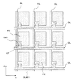
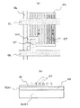
図1は、液晶表示装置の液晶を介して対向配置される各基板のうち一方の基板SUB1の液晶側の面の液晶表示領域に形成される回路の一実施例を示す構成図である。
<Example 1>
FIG. 1 is a configuration diagram showing an embodiment of a circuit formed in a liquid crystal display region on the liquid crystal side surface of one substrate SUB1 among the substrates arranged to face each other through the liquid crystal of the liquid crystal display device.
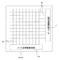
図1において、y方向に延在されx方向に並設されるソース信号線SLと、このソース信号線SLと絶縁されてx方向に延在されy方向に並設されるゲート信号線GLを有し、これら各信号線によって囲まれる矩形状の領域が画素の領域(図中点線枠で示す)に相当するようになっている。これにより、各画素はマトリックス状に配置され、この画素群によって前記液晶表示領域を構成するようになっている。 In FIG. 1, source signal lines SL extending in the y direction and arranged in parallel in the x direction, and gate signal lines GL insulated from the source signal lines SL and extending in the x direction and arranged in parallel in the y direction are shown. The rectangular area surrounded by these signal lines corresponds to a pixel area (indicated by a dotted frame in the figure). Thus, the pixels are arranged in a matrix, and the liquid crystal display area is configured by the pixel group.
各画素の領域にはその大部分にわたってたとえば透明電極からなる画素電極PXが形成され、この画素電極PXは薄膜トランジスタTFTを介してたとえば図中左側に隣接するソース信号線SLと接続されるようになっている。該薄膜トランジスタTFTは、そのオン、オフの駆動によって、ソース信号線SLからの信号を画素電極PXへの供給、非供給を制御するようになっている。 A pixel electrode PX made up of, for example, a transparent electrode is formed over most of each pixel region, and this pixel electrode PX is connected to the source signal line SL adjacent to the left side in the drawing through the thin film transistor TFT, for example. ing. The thin film transistor TFT controls the supply and non-supply of the signal from the source signal line SL to the pixel electrode PX by the on / off driving.
前記薄膜トランジスタTFTは、前記ゲート信号線GLの延在部で形成されるゲート電極GTが半導体層の上方に配置され、いわゆるトップゲート型と称されるMIS(Metal Insulator Semiconductor)構造となっている。 The thin film transistor TFT has a MIS (Metal Insulator Semiconductor) structure called a top gate type in which a gate electrode GT formed by an extension of the gate signal line GL is disposed above a semiconductor layer.
これにより、各ゲート信号線GLのそれぞれに信号(走査信号)が順次供給されることにより、画素列の各画素の薄膜トランジスタTFTがオンされ、そのオンのタイミングに応じて各ソース信号線SLにそれぞれ映像信号を供給することにより、この映像信号の電圧は前記画素列の各画素における画素電極PXに印加されるようになる。 As a result, a signal (scanning signal) is sequentially supplied to each of the gate signal lines GL, so that the thin film transistor TFT of each pixel in the pixel column is turned on, and each source signal line SL is applied to each of the source signal lines SL according to the turn-on timing. By supplying the video signal, the voltage of the video signal is applied to the pixel electrode PX in each pixel of the pixel column.
なお、この実施例に示す液晶表示装置は、前記基板SUB1と液晶を介して配置される図示しない他の基板を有し、この基板の液晶側の面には各画素に共通な対向電極が形成され、この対向電極はたとえば透明電極から構成され、前記ソース信号線SLに供給される信号(映像信号)に対して基準となる電圧からなる信号が供給されるようになっている。前記液晶には前記画素電極PXと対向電極の電位差によって発生する電界が印加され、該液晶の分子が挙動するようになっている。 The liquid crystal display device shown in this embodiment has the substrate SUB1 and another substrate (not shown) disposed through the liquid crystal, and a common electrode common to each pixel is formed on the liquid crystal side surface of the substrate. The counter electrode is formed of a transparent electrode, for example, and is supplied with a signal having a reference voltage with respect to a signal (video signal) supplied to the source signal line SL. An electric field generated by the potential difference between the pixel electrode PX and the counter electrode is applied to the liquid crystal, and the molecules of the liquid crystal behave.
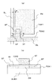
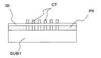
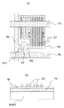
図2(a)は、図1に示した各画素のうち一の画素を抜き出して描いた図である。また、図2(b)は図2(a)のb−b線における断面図である。 FIG. 2A is a diagram illustrating one pixel extracted from each pixel illustrated in FIG. FIG. 2B is a cross-sectional view taken along the line bb in FIG.
図2において、ソース信号線SL、薄膜トランジスタTFTのソース領域部ST、チャネル領域部CH(ゲート電極GTの直下の部分)、ドレイン領域部DT、および画素電極PXは、最初、一体的に形成された同一層の第1透明酸化物層TOX1によって形成されるようになっている。 In FIG. 2, the source signal line SL, the source region ST of the thin film transistor TFT, the channel region CH (portion immediately below the gate electrode GT), the drain region DT, and the pixel electrode PX are first formed integrally. The first transparent oxide layer TOX1 is formed of the same layer.
すなわち、該第1透明酸化物層TOX1において、前記チャネル領域部CHはキャリア濃度が低くシート抵抗が高い膜(半導体層)として形成され、ソース信号線SL、薄膜トランジスタTFTのソース領域部ST、ドレイン領域部DT、および画素電極PXの形成領域はキャリア濃度が高くシート抵抗が低い膜(導電体層)として形成されている。この場合、たとえば、シート抵抗がソース信号線SL、画素電極PX<ソース領域部ST、ドレイン領域部DT<チャネル領域部CHという順で高くなるように形成してもよく、ソース信号線SL<画素電極PX、ソース領域部ST、ドレイン領域部DT<チャネル領域分CHという順で高くなるように形成してもよい。後者の場合、画素電極PXはキャリア濃度を比較的低くしてその透明度を損なうことなく形成できるという効果を奏する。 That is, in the first transparent oxide layer TOX1, the channel region CH is formed as a film (semiconductor layer) having a low carrier concentration and a high sheet resistance, and the source signal line SL, the source region ST of the thin film transistor TFT, the drain region The formation region of the part DT and the pixel electrode PX is formed as a film (conductor layer) having a high carrier concentration and a low sheet resistance. In this case, for example, the sheet resistance may be formed so as to increase in the order of the source signal line SL, the pixel electrode PX <the source region portion ST, the drain region portion DT <the channel region portion CH, and the source signal line SL <pixel. The electrode PX, the source region ST, and the drain region DT <channel region CH may be formed in this order. In the latter case, there is an effect that the pixel electrode PX can be formed without compromising the transparency by lowering the carrier concentration.
このように構成されたソース信号線SLと画素電極PXは第1透明酸化物層TOX1によって一体的にかつ同一層で形成されているため、それらの間隔(図中wで示す)を最小限に小さくすることができる。ソース信号線SLと画素電極PXを別個の工程で形成した場合と比較するとマスク合わせの限界によってそれらの間隔が大きくなってしまう不都合を解消できるからである。これにより、画素の開口率の向上を図った構成とすることができる。 Since the source signal line SL and the pixel electrode PX configured in this way are formed integrally and in the same layer by the first transparent oxide layer TOX1, their interval (indicated by w in the figure) is minimized. Can be small. This is because, compared with the case where the source signal line SL and the pixel electrode PX are formed in separate steps, it is possible to eliminate the disadvantage that the distance between the source signal line SL and the pixel electrode PX increases due to the limit of mask alignment. Thereby, it can be set as the structure which aimed at the improvement of the aperture ratio of a pixel.
ゲート信号線GLおよび薄膜トランジスタTFTのゲート電極GTは、たとえばITO(Indium Tin Oxide)あるいはキャリア濃度が高くシート抵抗が低いZnO等の第2透明酸化物層TOX2によって一体的にかつ同一層で形成されている。この場合、該ゲート信号線GLおよびゲート電極GTは上述のような透明酸化物層に限られることはなく、たとえば金属層によって形成するようにしてもよい。ゲート信号線GLの電気抵抗をさらに低減させたい場合にはそれに相当する材料の金属層を用いるのが適当だからである。 The gate signal line GL and the gate electrode GT of the thin film transistor TFT are formed integrally and in the same layer by a second transparent oxide layer TOX2 such as ITO (Indium Tin Oxide) or ZnO having a high carrier concentration and a low sheet resistance. Yes. In this case, the gate signal line GL and the gate electrode GT are not limited to the transparent oxide layer as described above, and may be formed of, for example, a metal layer. This is because, when it is desired to further reduce the electric resistance of the gate signal line GL, it is appropriate to use a metal layer of a material corresponding thereto.
また、前記第1透明酸化物膜TOX1は、基板SUB1の表面に形成され、その上面は絶縁膜GIによって被われ、前記ゲート電極GTは前記第1透明導電膜TOX1のチャネル領域部CHの上方に前記絶縁膜GIを介して配置されている。前記絶縁膜GIは薄膜トランジスタTFTのゲート絶縁膜として機能する。 The first transparent oxide film TOX1 is formed on the surface of the substrate SUB1, the upper surface thereof is covered with the insulating film GI, and the gate electrode GT is above the channel region portion CH of the first transparent conductive film TOX1. It is arranged via the insulating film GI. The insulating film GI functions as a gate insulating film of the thin film transistor TFT.
上述のように、前記第1透明酸化物層TOX1はキャリア濃度の高い領域とキャリア濃度の低い領域が領域的に区分けして形成され、前者を導電体層とし後者を半導体層として形成されたものとなっている。そこで、前記液晶表示装置の製造方法を説明する前に、透明酸化物層TOXにおいてキャリア濃度の高い領域を低い領域と区分けして選択的に形成する場合のいくつかの実施例について説明する。 As described above, the first transparent oxide layer TOX1 is formed by dividing a region having a high carrier concentration and a region having a low carrier concentration into regions, the former being a conductor layer and the latter being a semiconductor layer. It has become. Therefore, before explaining the manufacturing method of the liquid crystal display device, some examples in the case where the region having a high carrier concentration in the transparent oxide layer TOX is selectively formed separately from the low region will be described.
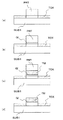
図3は、基板SUB1の上面に形成した透明酸化物層TOXにキャリア濃度の高い領域を選択的に形成する場合の一実施例を示した図である。 FIG. 3 is a diagram showing an example in which a region having a high carrier concentration is selectively formed in the transparent oxide layer TOX formed on the upper surface of the substrate SUB1.
図3(a)において、基板SUB1の上面に透明酸化物層TOXを形成し、その透明酸化物層TOXの表面の領域のうちキャリア濃度を高くする領域以外の領域にマスクとしてたとえばフォトレジスト膜PRTを形成する。 In FIG. 3A, a transparent oxide layer TOX is formed on the upper surface of the substrate SUB1, and, for example, a photoresist film PRT is used as a mask in a region other than the region where the carrier concentration is increased in the surface region of the transparent oxide layer TOX. Form.
そして、前記透明酸化物層TOXにレーザ光RLを照射する。このレーザ光RLとしてはたとえばKrFエキシマレーザを用いるのが好適であるが、他の光源であってもよい。これにより、該フォトレジスト膜PRTから露出された透明酸化物層TOXの領域は該光によって結晶改質がなされキャリア濃度を向上させた領域として形成することができる。 Then, the transparent oxide layer TOX is irradiated with a laser beam RL. As this laser light RL, for example, a KrF excimer laser is preferably used, but another light source may be used. As a result, the region of the transparent oxide layer TOX exposed from the photoresist film PRT can be formed as a region that has been crystal-modified by the light to improve the carrier concentration.
図3(b)は、透明酸化物層TOXにキャリア濃度の高い領域を光照射によって選択的に形成する場合の他の実施例を示し、透明酸化物層TOXの表面に予め絶縁膜GIを形成しておき、この絶縁膜GIを通してレーザ光RLを前記透明酸化物層TOXに照射することが図3(a)の場合と異なっている。 FIG. 3B shows another example in which a region having a high carrier concentration is selectively formed on the transparent oxide layer TOX by light irradiation, and an insulating film GI is previously formed on the surface of the transparent oxide layer TOX. In addition, the laser beam RL is irradiated to the transparent oxide layer TOX through the insulating film GI, which is different from the case of FIG.
図3(c)は、透明酸化物層TOXにキャリア濃度の高い領域を光照射によって選択的に形成する場合の他の実施例を示し、透明酸化物TOXが絶縁膜GIで被われ、この絶縁膜GIの一部の領域において形成されたたとえば電極TMおよび該電極TMに積層されたフォトレジスト膜PRTをマスクとして、レーザ光RLを前記透明酸化物層TOXに照射することが図3(b)の場合と異なっている。 FIG. 3C shows another embodiment in which a region having a high carrier concentration is selectively formed on the transparent oxide layer TOX by light irradiation. The transparent oxide TOX is covered with an insulating film GI, and this insulation is performed. For example, the transparent oxide layer TOX may be irradiated with the laser light RL using, for example, the electrode TM formed in a partial region of the film GI and the photoresist film PRT laminated on the electrode TM as a mask. It is different from the case of.
図3(d)は、透明酸化物層TOXにキャリア濃度の高い領域を光照射によって選択的に形成する場合の他の実施例を示し、図3(c)に示す電極TMを形成するためのフォトレジスタ膜PRTを除去した後に前記電極TMをマスクとして、レーザ光PLを前記透明酸化物層TOXに照射することが図3(c)の場合と異なっている。 FIG. 3D shows another embodiment in the case where a region having a high carrier concentration is selectively formed in the transparent oxide layer TOX by light irradiation, for forming the electrode TM shown in FIG. Unlike the case of FIG. 3C, the transparent oxide layer TOX is irradiated with the laser beam PL using the electrode TM as a mask after removing the photoresist film PRT.
図4は、基板SUB1の上面に形成した透明酸化物層TOXにキャリア濃度の高い領域を選択的に形成する場合の他の実施例を示した図である。 FIG. 4 is a diagram showing another embodiment in the case where a region having a high carrier concentration is selectively formed in the transparent oxide layer TOX formed on the upper surface of the substrate SUB1.
図4(a)において、基板SUB1の上面に透明酸化物層TOXを形成し、その透明酸化物層TOXの表面の領域のうちキャリア濃度を高くする領域以外の領域にマスクとしてたとえばフォトレジスト膜PRTを形成する。 In FIG. 4A, a transparent oxide layer TOX is formed on the upper surface of the substrate SUB1, and, for example, a photoresist film PRT is used as a mask in a region other than the region where the carrier concentration is increased in the surface region of the transparent oxide layer TOX. Form.
そして、前記透明酸化物層TOXに前記フォトレジスト膜PRTを残したまま還元雰囲気下において熱アニールを施す。 Then, thermal annealing is performed in a reducing atmosphere while leaving the photoresist film PRT on the transparent oxide layer TOX.
これにより、該フォトレジスト膜PRTから露出された透明酸化物層TOXの領域は該熱アニールによって結晶改質がなされキャリア濃度を向上させた領域として形成することができる。 Thereby, the region of the transparent oxide layer TOX exposed from the photoresist film PRT can be formed as a region whose crystal concentration has been improved by the thermal annealing and the carrier concentration has been improved.
図4(b)は、透明酸化物層TOXにキャリア濃度の高い領域を熱アニールによって選択的に形成する場合の他の実施例を示し、透明酸化物層TOXの表面に選択的に形成された絶縁膜GIとこの絶縁膜GIの上面に形成され該絶縁膜GIを選択的に形成する際に用いられたフォトレジスト膜PRTを残したまま熱アニールを施すことが図4(a)の場合と異なっている。 FIG. 4B shows another example in which a region having a high carrier concentration is selectively formed in the transparent oxide layer TOX by thermal annealing, and is selectively formed on the surface of the transparent oxide layer TOX. In the case of FIG. 4A, thermal annealing is performed while leaving the insulating film GI and the photoresist film PRT formed on the upper surface of the insulating film GI and used for selectively forming the insulating film GI. Is different.
図4(c)は、透明酸化物層TOXにキャリア濃度の高い領域を熱アニールによって選択的に形成する場合の他の実施例を示し、透明酸化物層TOXの表面に選択的に形成された絶縁膜GIおよび電極TMの積層体とこの積層体の上面に形成され該電極TMおよび絶縁膜GIを形成する際に用いられたフォトレジスト膜PRTを残したまま熱アニールを施すことが図4(b)の場合と異なっている。 FIG. 4C shows another example in which a region having a high carrier concentration is selectively formed in the transparent oxide layer TOX by thermal annealing, and is selectively formed on the surface of the transparent oxide layer TOX. It is possible to perform thermal annealing while leaving the laminated body of the insulating film GI and the electrode TM and the photoresist film PRT formed on the upper surface of the laminated body and used for forming the electrode TM and the insulating film GI as shown in FIG. It is different from the case of b).
図4(d)は、透明酸化物層TOXにキャリア濃度の高い領域を熱アニールによって選択的に形成する場合の他の実施例を示し、透明酸化物層TOXの表面に選択的に形成された絶縁膜GIおよび電極TMの積層体を形成する際に用いられたフォトレジスト膜PRTを除去した状態で熱アニールを施すことが図4(c)の場合と異なっている。 FIG. 4 (d) shows another embodiment in which a region having a high carrier concentration is selectively formed in the transparent oxide layer TOX by thermal annealing, and is selectively formed on the surface of the transparent oxide layer TOX. Unlike the case of FIG. 4C, thermal annealing is performed in a state where the photoresist film PRT used for forming the laminated body of the insulating film GI and the electrode TM is removed.
図5は、基板SUB1の上面に形成した透明酸化物層TOXにキャリア濃度の高い領域を選択的に形成する場合の他の実施例を示した図である。 FIG. 5 is a view showing another embodiment in the case where a region having a high carrier concentration is selectively formed in the transparent oxide layer TOX formed on the upper surface of the substrate SUB1.
図5(a)において、基板SUB1の上面に透明酸化物層TOXを形成し、その透明酸化物層TOXの表面の領域のうちキャリア濃度を高くする領域以外の領域にマスクとしてたとえばフォトレジスト膜PRTを形成する。 In FIG. 5A, a transparent oxide layer TOX is formed on the upper surface of the substrate SUB1, and, for example, a photoresist film PRT is used as a mask in a region other than the region where the carrier concentration is increased in the surface region of the transparent oxide layer TOX. Form.
そして、前記透明酸化物層TOXに不純物イオンNPIを注入する。この不純物イオンNPIとしては必要に応じてn型あるいはp型が使用される。 Then, impurity ions NPI are implanted into the transparent oxide layer TOX. As this impurity ion NPI, n-type or p-type is used as necessary.
これにより、該フォトレジスト膜PRTから露出された透明酸化物層TOXの領域は該不純物イオンNPIの注入によってキャリア濃度を向上させた領域として形成することができる。 Thereby, the region of the transparent oxide layer TOX exposed from the photoresist film PRT can be formed as a region whose carrier concentration is improved by the implantation of the impurity ions NPI.
図5(b)は、基板SUB1の上面に形成した透明酸化物層TOXにキャリア濃度の高い領域を不純物イオンNPIの注入によって形成する場合の他の実施例を示した図である。透明酸化物層TOXの表面に予め絶縁膜GIを形成しておき、この絶縁膜GIを通して不純物イオンNPIの注入を前記透明酸化物層TOXに行っていることが図5(a)の場合と異なっている。 FIG. 5B is a diagram showing another example in which a region having a high carrier concentration is formed by implantation of impurity ions NPI in the transparent oxide layer TOX formed on the upper surface of the substrate SUB1. Unlike the case of FIG. 5A, an insulating film GI is formed in advance on the surface of the transparent oxide layer TOX, and impurity ions NPI are injected into the transparent oxide layer TOX through the insulating film GI. ing.
図5(c)は、透明酸化物層TOXにキャリア濃度の高い領域を不純物イオンNPIの注入によって形成する場合の他の実施例を示し、透明酸化物層TOXが絶縁膜GIで被われ、この絶縁膜GIの一部の領域において形成されたたとえば電極TMおよび該電極TMに積層されたフォトレジスト膜PRTをマスクとして、不純物イオンNPIの注入を前記透明酸化物層TOXに行っていることが図5(b)の場合と異なっている。 FIG. 5C shows another example of forming a region having a high carrier concentration in the transparent oxide layer TOX by implantation of impurity ions NPI. The transparent oxide layer TOX is covered with an insulating film GI. The impurity ions NPI are implanted into the transparent oxide layer TOX using, for example, the electrode TM formed in a partial region of the insulating film GI and the photoresist film PRT laminated on the electrode TM as a mask. This is different from the case of 5 (b).
図5(d)は、透明酸化物層TOXにキャリア濃度の高い領域を不純物イオンNPIの注入によって形成する場合の他の実施例を示し、図5(c)に示す電極TMを形成するためのフォトレジスタ膜PRTを除去した後に前記電極TMをマスクとして、不純物イオンNPIの注入を前記透明酸化物層TOXに行っていることが図5(c)の場合と異なっている。 FIG. 5D shows another embodiment in which a region having a high carrier concentration is formed in the transparent oxide layer TOX by implantation of impurity ions NPI, and the electrode TM shown in FIG. 5C is formed. Unlike the case of FIG. 5C, impurity ions NPI are implanted into the transparent oxide layer TOX using the electrode TM as a mask after removing the photoresist film PRT.
図6は、基板SUB1の上面に形成した透明酸化物層TOXにキャリア濃度の高い領域を選択的に形成する場合の他の実施例を示した図である。 FIG. 6 is a view showing another embodiment in the case where a region having a high carrier concentration is selectively formed in the transparent oxide layer TOX formed on the upper surface of the substrate SUB1.
図6(a)において、基板SUB1の上面に透明酸化物層TOXを形成し、その透明酸化物層TOXの表面の領域のうちキャリア濃度を高くする領域以外の領域にマスクとしてたとえばフォトレジスト膜PRTを形成する。 In FIG. 6A, a transparent oxide layer TOX is formed on the upper surface of the substrate SUB1, and, for example, a photoresist film PRT is used as a mask in a region other than the region where the carrier concentration is increased in the surface region of the transparent oxide layer TOX. Form.
そして、前記マスクから露出された透明酸化物層TOXの表面にn型あるいはp型の不純物からなるドーパント原料DMを堆積する。 Then, a dopant material DM made of n-type or p-type impurities is deposited on the surface of the transparent oxide layer TOX exposed from the mask.
さらに、前記透明酸化物層TOXにレーザ光RLの照射(あるいは熱アニール)を行う。このレーザ光RLとしてはたとえばKrFエキシマレーザを用いるのが好適であるが、他の光源であってもよい。 Further, the transparent oxide layer TOX is irradiated with laser light RL (or thermal annealing). As this laser light RL, for example, a KrF excimer laser is preferably used, but another light source may be used.
これにより、該フォトレジスト膜PRTから露出された透明酸化物層TOXの領域は該ドーパント原料DMの拡散がなされキャリア濃度を向上させた領域として形成することができる。 Thus, the region of the transparent oxide layer TOX exposed from the photoresist film PRT can be formed as a region in which the dopant raw material DM is diffused and the carrier concentration is improved.
図6(b)は、透明酸化物層TOXにキャリア濃度の高い領域をドーパント原料DMの拡散によって形成する場合の他の実施例を示し、透明酸化物層TOXの表面に選択的に形成された絶縁膜GIとこの絶縁膜GIの上面に形成され該絶縁膜GIを選択的に形成する際に用いられたフォトレジスト膜PRTを残したままレーザ光RLの照射(あるいは熱アニール)を行うことが図6(a)の場合と異なっている。 FIG. 6B shows another example in which a region having a high carrier concentration is formed in the transparent oxide layer TOX by diffusion of the dopant raw material DM, and is selectively formed on the surface of the transparent oxide layer TOX. Irradiation (or thermal annealing) of the laser beam RL may be performed while leaving the insulating film GI and the photoresist film PRT formed on the upper surface of the insulating film GI and used to selectively form the insulating film GI. This is different from the case of FIG.
図6(c)は、透明酸化物層TOXにキャリア濃度の高い領域をドーパント原料DMの拡散によって形成する場合の他の実施例を示し、透明酸化物層TOXの表面に選択的に形成された絶縁膜GIおよび電極TMの積層体とこの積層体の上面に形成され該電極TMおよび絶縁膜GIを形成する際に用いられたフォトレジスト膜PRTを残したままレーザ光RLの照射(あるいは熱アニール)を行うことが図6(b)の場合と異なっている。 FIG. 6C shows another example in which a region having a high carrier concentration is formed in the transparent oxide layer TOX by diffusion of the dopant raw material DM, and is selectively formed on the surface of the transparent oxide layer TOX. Irradiation (or thermal annealing) of the laminated body of the insulating film GI and the electrode TM and the laser beam RL while leaving the photoresist film PRT formed on the upper surface of the laminated body and used for forming the electrode TM and the insulating film GI ) Is different from the case of FIG.
図6(d)は、透明酸化物層TOXにキャリア濃度の高い領域をドーパント原料DMの拡散によって形成する場合の他の実施例を示し、透明酸化物層TOXの表面に選択的に形成された絶縁膜GIおよび電極TMの積層体を形成する際に用いられたフォトレジスト膜PRTを除去した状態でレーザ光RLの照射(あるいは熱アニール)を行うことが図6(c)の場合と異なっている。 FIG. 6D shows another example of forming a region having a high carrier concentration in the transparent oxide layer TOX by diffusion of the dopant raw material DM, and is selectively formed on the surface of the transparent oxide layer TOX. Unlike the case of FIG. 6C, the laser beam RL is irradiated (or thermally annealed) in a state where the photoresist film PRT used for forming the laminated body of the insulating film GI and the electrode TM is removed. Yes.
次に、前記液晶表示装置の製造方法を説明するが、その工程の際において、透明酸化物層にキャリア濃度の高い領域を低い領域と区分けして選択的に形成する場合、上述した図3〜図6に示した何れかの手法を採用してもよい。以下の説明では、たとえばレーザ光の照射による手法を例に挙げて説明をする。 Next, a method for manufacturing the liquid crystal display device will be described. In the process, when the transparent oxide layer is selectively formed by dividing a region having a high carrier concentration from a low region, the above-described FIG. Any of the methods shown in FIG. 6 may be adopted. In the following description, for example, a method using laser light irradiation will be described as an example.
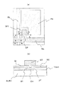
図8は、液晶表示装置の製造方法の一実施例を示す工程図である。ここで、図8に示す工程は液晶表示領域の一画素における工程図を示し、図8の左側に示す工程図は図7のL−L線の個所に相当し、図8の右側に示す工程図は図7のR−R線の個所に相当している。なお、図7に示す画素は図2に示した画素と同じである。 FIG. 8 is a process diagram showing an embodiment of a method for manufacturing a liquid crystal display device. Here, the process shown in FIG. 8 is a process diagram in one pixel of the liquid crystal display region, and the process diagram shown on the left side of FIG. 8 corresponds to the part of line LL in FIG. 7, and the process shown on the right side of FIG. The figure corresponds to the location of line RR in FIG. Note that the pixel shown in FIG. 7 is the same as the pixel shown in FIG.
また、以下の工程では、薄膜トランジスタTFTのチャネル領域部CHのソース領域部STおよびドレイン領域部DTへの各側にLDD領域部を形成する場合も併せて示している。ここで、LDD領域部はゲート電極GTとの間において電界緩和を行うように機能する。 In the following process, a case where an LDD region portion is formed on each side of the channel region portion CH of the thin film transistor TFT to the source region portion ST and the drain region portion DT is also shown. Here, the LDD region portion functions to perform electric field relaxation with the gate electrode GT.
以下、工程順に説明する。 Hereinafter, it demonstrates in order of a process.
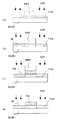
工程1.
図8(a)に示すように、たとえばガラスからなる基板SUB1を用意し、この基板SUB1の表面(液晶側の面)にたとえばZnO等からなる高抵抗の第1透明酸化物層TOX1およびたとえばSiO2等からなる第1絶縁膜GI1を順次成膜する。ここで、前記第1絶縁膜GI1は薄膜トランジスタTFTの形成領域においてそのゲート絶縁膜として機能するようになっている。
Step 1.
As shown in FIG. 8A, a substrate SUB1 made of, for example, glass is prepared, and a high-resistance first transparent oxide layer TOX1 made of, for example, ZnO or the like is formed on the surface (surface on the liquid crystal side) of this substrate SUB1 and, for example, SiO. A first insulating film GI1 made of 2 or the like is sequentially formed. Here, the first insulating film GI1 functions as a gate insulating film in a region where the thin film transistor TFT is formed.
工程2.
図8(b)に示すように、前記第1絶縁膜GI1の上面の全域に第1フォトレジスト膜PRT1を形成し、この第1フォトレジスト膜PRT1を所定のパターンに形成する。
Step 2.
As shown in FIG. 8B, a first photoresist film PRT1 is formed over the entire upper surface of the first insulating film GI1, and the first photoresist film PRT1 is formed in a predetermined pattern.
ここで、パターン化された第1フォトレジスト膜PRT1は、図7に示す画素のうち、ソース信号線SL、このソース信号線SLと接続される薄膜トランジスタTFT、この薄膜トランジスタTFTと接続される画素電極PXを形成すべく領域に形成され、かつ、前記薄膜トランジスタTFTのチャネル領域部およびその両脇のいわゆるLDD領域(電界緩和領域)の形成領域において高くそれ以外の部分が低いというように二段の高低を有するようにして形成されている。 Here, the patterned first photoresist film PRT1 includes a source signal line SL, a thin film transistor TFT connected to the source signal line SL, and a pixel electrode PX connected to the thin film transistor TFT among the pixels shown in FIG. In the region where the thin film transistor TFT is to be formed, and in the formation region of the so-called LDD region (electric field relaxation region) on both sides of the thin film transistor TFT. It is formed to have.
このような高低差のある第1フォトレジスト膜PRT1は、たとえば遮光、いわゆる半透光、透光の3段階からなる透光量の異なるフォトマスクを用いて前記第1フォトレジスト膜PRT1を感光することによって形成される。このような第1フォトレジスト膜PRT1はいわゆるハーフトーンマスクあいはグレートーンマスクを用いた露光によって形成することができる。 The first photoresist film PRT1 having such a height difference is exposed to the first photoresist film PRT1 by using, for example, a photomask having different light transmission amounts including three stages of light shielding, so-called semi-light transmission and light transmission. Formed by. Such a first photoresist film PRT1 can be formed by exposure using a so-called halftone mask or gray tone mask.
そして、このように形成された第1フォトレジスト膜PRT1をマスクとし、このマスクから露出された第1絶縁膜GI1およびこの第1絶縁膜GI1の下層の第1透明酸化物層TOX1を順次エッチングし、基板SUB1の表面を露出させる。 The first photoresist film PRT1 thus formed is used as a mask, and the first insulating film GI1 exposed from the mask and the first transparent oxide layer TOX1 under the first insulating film GI1 are sequentially etched. Then, the surface of the substrate SUB1 is exposed.
このようにして第1透明酸化物層TOXと第1絶縁膜GI1の積層体は、ソース信号線SL、このソース信号線SLと接続される薄膜トランジスタTFT、この薄膜トランジスタTFTと接続される画素電極PXの形成領域に残存される。 Thus, the stacked body of the first transparent oxide layer TOX and the first insulating film GI1 includes the source signal line SL, the thin film transistor TFT connected to the source signal line SL, and the pixel electrode PX connected to the thin film transistor TFT. It remains in the formation area.
工程3.
図8(c)に示すように、前記第1フォトレジスト膜PRT1の表面を底面方向に適当量の除去を行うことによって、該第1フォトレジスト膜PRT1を、ソース信号線SL、このソース信号線SLと接続される薄膜トランジスタTFT(そのチャネル領域部およびLDD領域部の部分を除く)、この薄膜トランジスタTFTと接続される画素電極PXの各形成領域において完全に除去し、前記薄膜トランジスタTFTのチャネル領域部およびLDD領域部の形成領域にのみ残存させるようにする。
Step 3.
As shown in FIG. 8C, by removing an appropriate amount of the surface of the first photoresist film PRT1 in the bottom direction, the first photoresist film PRT1 is formed into a source signal line SL, and the source signal line SL. The thin film transistor TFT connected to the SL (excluding the channel region portion and the LDD region portion) and the pixel electrode PX connected to the thin film transistor TFT are completely removed in the channel region portion of the thin film transistor TFT and It is made to remain only in the formation region of the LDD region.
そして、第1絶縁膜GI1を通して第1透明酸化物層TOX1にたとえばレーザ光RLを照射することによって該第1透明酸化物層TOX1に結晶改質を行う。該第1透明酸化物層TOX1にキャリア濃度を向上させ低抵抗化を図るためである。この場合、前記第1フォトレジスト膜PRT1が形成されている部分においてレーザ光RLの照射が阻止され該第1フォトレジスト膜RLの直下の第1透明酸化物層TOX1は高抵抗が維持される。 Then, crystal modification is performed on the first transparent oxide layer TOX1 by, for example, irradiating the first transparent oxide layer TOX1 with the laser light RL through the first insulating film GI1. This is because the first transparent oxide layer TOX1 has a higher carrier concentration and a lower resistance. In this case, the irradiation with the laser beam RL is blocked at the portion where the first photoresist film PRT1 is formed, and the first transparent oxide layer TOX1 immediately below the first photoresist film RL maintains a high resistance.
このことから、ソース信号線SL、このソース信号線SLと接続される薄膜トランジスタTFT(そのチャネル領域部およびLDD領域部の部分を除く)、この薄膜トランジスタTFTと接続される画素電極PXの各形成領域においてキャリア濃度を高めて導電体化し、前記薄膜トランジスタTFTのチャネル領域の部分においてキャリア濃度が低い半導体のまま残ることになる。 Therefore, in each formation region of the source signal line SL, the thin film transistor TFT connected to the source signal line SL (excluding the channel region portion and the LDD region portion), and the pixel electrode PX connected to the thin film transistor TFT. The carrier concentration is increased to form a conductor, and the semiconductor having a low carrier concentration remains in the channel region portion of the thin film transistor TFT.
工程4.
図8(d)に示すように、前記第1フォトレジスト膜PRT1を全て除去する。
Step 4.
As shown in FIG. 8D, the first photoresist film PRT1 is completely removed.
工程5.
図8(e)に示すように、たとえばSiO2からなる第2絶縁膜GI2、たとえばITO(Indium Tin Oxide)からなる第2透明酸化物層TOX2を順次成膜する。ここで、前記第2絶縁膜GI2は、ソース信号線SLに対する後述のゲート信号線GLの層間絶縁膜として機能するようになる。
Step 5.
As shown in FIG. 8E, a second insulating film GI2 made of, for example, SiO 2 , for example, a second transparent oxide layer TOX2 made of, for example, ITO (Indium Tin Oxide), is sequentially formed. Here, the second insulating film GI2 functions as an interlayer insulating film of a gate signal line GL to be described later with respect to the source signal line SL.
工程6.
図8(f)に示すように、前記第2透明酸化物層TOX2の上面に第2フォトレジスト膜PRT2を形成し、この第2フォトレジスト膜PRT2を所定のパターンに形成する。すなわち、ゲート信号線GL、このゲート信号線GLと接続される前記薄膜トランジスタTFTのゲート電極GTの各形成領域に前記第2フォトレジスト膜を残存させる。ここで、ゲート電極GTの形成領域は、薄膜トランジスタTFTのチャネル領域部の直上の部分であり、該チャネル領域の両脇のLDD領域は除かれる。
Step 6.
As shown in FIG. 8F, a second photoresist film PRT2 is formed on the upper surface of the second transparent oxide layer TOX2, and the second photoresist film PRT2 is formed in a predetermined pattern. That is, the second photoresist film is left in each formation region of the gate signal line GL and the gate electrode GT of the thin film transistor TFT connected to the gate signal line GL. Here, the formation region of the gate electrode GT is a portion immediately above the channel region portion of the thin film transistor TFT, and the LDD regions on both sides of the channel region are excluded.
そして、この第2フォトレジスト膜PRT2から露出された第2透明酸化物層TOX2をエッチングし、残存された第2透明酸化物層TOX2によって前記ゲート信号線SLおよびゲート電極Tを構成する。 Then, the second transparent oxide layer TOX2 exposed from the second photoresist film PRT2 is etched, and the gate signal line SL and the gate electrode T are constituted by the remaining second transparent oxide layer TOX2.
さらに、前記第2フォトレジスト膜PRT2をそのまま残存させ、第2絶縁膜GI2、第1絶縁膜GI1を通して第1透明酸化物層TOX1にレーザ光RLを照射する。 Further, the second photoresist film PRT2 is left as it is, and the first transparent oxide layer TOX1 is irradiated with the laser light RL through the second insulating film GI2 and the first insulating film GI1.
このレーザ光RLの照射によって、薄膜トランジスタTFTのチャネル領域部CHの両脇のLDD領域LDにおいてキャリア濃度が高められるようになる。この場合、前記工程3においてキャリア濃度が高められた第1透明酸化物層TOX1の部分においてもさらにキャリア濃度が高められることから、相対的に観て前記LDD領域LDは比較的導電性の小さな領域として形成されることになる。 The irradiation with the laser light RL increases the carrier concentration in the LDD regions LD on both sides of the channel region portion CH of the thin film transistor TFT. In this case, since the carrier concentration is further increased in the portion of the first transparent oxide layer TOX1 in which the carrier concentration is increased in the step 3, the LDD region LD is a region having a relatively low conductivity as viewed relatively. Will be formed.
工程7.
図8(g)に示すように、前記第2フォトレジスト膜PRT2を全て除去する。その後は、基板SUB1の表面に図示せぬ配向膜を形成することによって完了する。
Step 7.
As shown in FIG. 8G, the second photoresist film PRT2 is completely removed. Thereafter, the alignment is completed by forming an alignment film (not shown) on the surface of the substrate SUB1.
上述のように、基板SUB1の液晶側の面の液晶表示領域は、前記第1フォトレジスト膜PRT1および第2フォトレジスト膜PRT2を用いたいわゆる2フォト工程で製造することができる。 As described above, the liquid crystal display region on the liquid crystal side surface of the substrate SUB1 can be manufactured by a so-called two-photo process using the first photoresist film PRT1 and the second photoresist film PRT2.
また、第1フォトレジスト膜PRT1は、第1透明酸化物層TOX1および第1絶縁膜GI1の順次積層体の選択エッチングの際のマスク、および前記第1透明酸化物層TOX1におけるキャリア濃度の高い領域の選択的形成の際のマスクとしてそれぞれ機能するが、フォトリソグラフィ技術の適用は一回で済むことになり、工程の大幅低減を図ることができる。 The first photoresist film PRT1 includes a mask for selective etching of the first transparent oxide layer TOX1 and the first insulating film GI1 and a region having a high carrier concentration in the first transparent oxide layer TOX1. Each of them functions as a mask in the selective formation, but the application of the photolithography technique is only required once, and the process can be greatly reduced.
図9は、前記液晶表示装置の製造方法の他の実施例を示す工程図である。図9は、図8と対応した図となっており、したがって、図9の左側に示す工程図は図7のL−L線の個所に相当し、図9の右側に示す工程図は図7のR−Rの個所に相当している。 FIG. 9 is a process diagram showing another embodiment of the method for manufacturing the liquid crystal display device. 9 corresponds to FIG. 8. Therefore, the process diagram shown on the left side of FIG. 9 corresponds to the part of line LL in FIG. 7, and the process diagram shown on the right side of FIG. This corresponds to the R-R portion.
以下、工程順に説明する。 Hereinafter, it demonstrates in order of a process.
工程1.
図9(a)に示すように、基板SUB1を用意し、この基板SUB1の表面(液晶側の面)にたとえばZnO等からなる高抵抗の第1透明酸化物層TOX1およびたとえばSiO2等からなる第1絶縁膜GI1を順次成膜する。
Step 1.
As shown in FIG. 9A, a substrate SUB1 is prepared, and the surface (liquid crystal side surface) of the substrate SUB1 is made of a high-resistance first transparent oxide layer TOX1 made of ZnO or the like, and SiO 2 or the like. The first insulating film GI1 is sequentially formed.
工程2.
図9(b)に示すように、前記第1絶縁膜GI1の上面の全域に第1フォトレジスト膜PRT1を形成し、この第1フォトレジスト膜PRT1を所定のパターンに形成する。
Step 2.
As shown in FIG. 9B, a first photoresist film PRT1 is formed over the entire upper surface of the first insulating film GI1, and the first photoresist film PRT1 is formed in a predetermined pattern.
ここで、パターン化された第1フォトレジスト膜PRT1は、図7に示す画素のうち、ソース信号線SL、このソース信号線SLと接続される薄膜トランジスタTFT、この薄膜トランジスタTFTと接続される画素電極PXの各形成領域に形成され、かつ、ソース信号線SLの部分が低くそれ以外の部分が高いというように二段の高低を有するようにして形成されている。 Here, the patterned first photoresist film PRT1 includes a source signal line SL, a thin film transistor TFT connected to the source signal line SL, and a pixel electrode PX connected to the thin film transistor TFT among the pixels shown in FIG. Are formed so as to have two levels of height such that the portion of the source signal line SL is low and the other portions are high.
そして、前記第1フォトレジスト膜PRT1をマスクとし、このマスクから露出された第1絶縁膜GI1およびこの第1絶縁膜GI1の下層の第1透明酸化物層TOX1を順次エッチングし、基板SUB1の表面を露出させる。 Then, using the first photoresist film PRT1 as a mask, the first insulating film GI1 exposed from the mask and the first transparent oxide layer TOX1 under the first insulating film GI1 are sequentially etched, and the surface of the substrate SUB1 To expose.
このようにして第1透明酸化物層TOX1と第1絶縁膜GI1の積層体は、ソース信号線SL、このソース信号線SLと接続される薄膜トランジスタTFT、この薄膜トランジスタTFTと接続される画素電極PXの形成領域に残存される。 Thus, the stacked body of the first transparent oxide layer TOX1 and the first insulating film GI1 includes the source signal line SL, the thin film transistor TFT connected to the source signal line SL, and the pixel electrode PX connected to the thin film transistor TFT. It remains in the formation area.
工程3.
図9(c)に示すように、前記第1フォトレジスト膜PRT1の表面を底面方向に適当量の除去を行うことによって、該第1フォトレジスト膜PRT1を、ソース信号線SLの形成領域において完全に除去し、前記薄膜トランジスタTFTのチャネル領域部、このチャネル領域部に隣接しソース信号線SL側のLDD領域部、および画素電極PXの各形成領域にのみ残存させるようにする。
Step 3.
As shown in FIG. 9C, by removing an appropriate amount of the surface of the first photoresist film PRT1 in the bottom direction, the first photoresist film PRT1 is completely removed in the source signal line SL formation region. The thin film transistor TFT is left only in the formation region of the channel region portion of the thin film transistor TFT, the LDD region portion adjacent to the channel region portion and on the source signal line SL side, and the pixel electrode PX.
そして、第1絶縁膜GI1を通して第1透明酸化物層TOX1にレーザ光RLを照射することによって該第1透明酸化物層TOX1に結晶改質を行う。この場合、前記第1フォトレジスト膜PRT1が形成されている部分においてレーザ光RLの照射が阻止され該第1フォトレジスト膜PRT1の直下の第1透明酸化物層TOX1は高抵抗が維持される。 Then, crystal modification is performed on the first transparent oxide layer TOX1 by irradiating the first transparent oxide layer TOX1 with the laser light RL through the first insulating film GI1. In this case, the irradiation with the laser beam RL is blocked at the portion where the first photoresist film PRT1 is formed, and the first transparent oxide layer TOX1 immediately below the first photoresist film PRT1 maintains a high resistance.
工程4.
図9(d)に示すように、前記第1フォトレジスト膜PRT1を全て除去する。
Step 4.
As shown in FIG. 9D, the first photoresist film PRT1 is completely removed.
工程5.
図9(e)に示すように、たとえばSiO2からなる第2絶縁膜GI2、たとえばITO(Indium Tin Oxide)からなる第2透明酸化物層TOX2を順次成膜する。
Step 5.
As shown in FIG. 9E, a second insulating film GI2 made of, for example, SiO 2 , for example, a second transparent oxide layer TOX2 made of, for example, ITO (Indium Tin Oxide), is sequentially formed.
工程6.
図9(f)に示すように、前記第2透明酸化物層TOX2の上面に第2フォトレジスト膜PRT2を形成し、この第2フォトレジスト膜PRT2を所定のパターンに形成する。すなわち、ゲート信号線GL、このゲート信号線GLと接続される前記薄膜トランジスタTFTのゲート電極GTの各形成領域に前記第2フォトレジスト膜PRT2を残存させる。ここで、ゲート電極GTの形成領域は、薄膜トランジスタTFTのチャネル領域部の直上の部分であり、該チャネル領域部に隣接するソース信号線SL側のLDD領域LDは除かれる。
Step 6.
As shown in FIG. 9F, a second photoresist film PRT2 is formed on the upper surface of the second transparent oxide layer TOX2, and the second photoresist film PRT2 is formed in a predetermined pattern. That is, the second photoresist film PRT2 is left in each formation region of the gate signal line GL and the gate electrode GT of the thin film transistor TFT connected to the gate signal line GL. Here, the formation region of the gate electrode GT is a portion immediately above the channel region portion of the thin film transistor TFT, and the LDD region LD on the source signal line SL side adjacent to the channel region portion is excluded.
そして、この第2フォトレジスト膜PRT2から露出された第2透明酸化物層TOX2をエッチングし、残存された第2透明酸化物層TOX2によって前記ゲート信号線GLおよびゲート電極GTを構成する。 Then, the second transparent oxide layer TOX2 exposed from the second photoresist film PRT2 is etched, and the gate signal line GL and the gate electrode GT are constituted by the remaining second transparent oxide layer TOX2.
さらに、前記第2フォトレジスト膜PRT2をそのまま残存させ、第2絶縁膜GI2、第1絶縁膜GI1を通して第1透明酸化物層TOX1にレーザ光RLを照射する。 Further, the second photoresist film PRT2 is left as it is, and the first transparent oxide layer TOX1 is irradiated with the laser light RL through the second insulating film GI2 and the first insulating film GI1.
このレーザ光RLの照射によって、薄膜トランジスタTFTのチャネル領域部に隣接するソース信号線SL側のLDD領域LDにおいてキャリア濃度が高められるようになる。この場合、前記工程3においてキャリア濃度が高められた第1透明酸化物層TOX1の部分においてもさらにキャリア濃度が高められることから、相対的に観て前記LDD領域LDは比較的導電性の小さな領域として形成されることになる。 By irradiation with the laser light RL, the carrier concentration is increased in the LDD region LD on the source signal line SL side adjacent to the channel region portion of the thin film transistor TFT. In this case, since the carrier concentration is further increased in the portion of the first transparent oxide layer TOX1 in which the carrier concentration is increased in the step 3, the LDD region LD is a region having a relatively low conductivity as viewed relatively. Will be formed.
さらに、薄膜トランジスタTFTのチャネル領域部に隣接する画素電極PXの部分において、ソース信号線SL側のLDD領域LDの形成領域と同様に相対的に観て比較的導電性の小さな領域として形成されることになる。画素電極PXは、図示しない他の電極(対向電極)との間で電界を生じせしめる電極として機能することから導電性が比較的に小さくてもよいことに基づくものである。そして、ZnO等の第1透明酸化物層TOX1は、キャリア濃度を高め過ぎると金属化してしまいもはや透明でなくなるが、前記画素電極PXにおいては透明を維持できる程度のキャリア濃度にできる効果を奏する。 Further, in the portion of the pixel electrode PX adjacent to the channel region portion of the thin film transistor TFT, it is formed as a region having a relatively small conductivity as viewed in the same manner as the formation region of the LDD region LD on the source signal line SL side. become. Since the pixel electrode PX functions as an electrode that generates an electric field with another electrode (counter electrode) (not shown), the pixel electrode PX is based on the fact that the conductivity may be relatively small. The first transparent oxide layer TOX1 such as ZnO is metalized when the carrier concentration is increased too much and is no longer transparent. However, in the pixel electrode PX, there is an effect that the carrier concentration can be maintained so as to maintain transparency.
なお、図8、図9に示した製造方法において、第1透明酸化物層TOX1にキャリア濃度の高い領域を形成する場合に、レーザ光RLの照射を一実施例として挙げたものであるが、図3〜図6に示す方法、あるいは他の方法を用いてもよいことは上述したとおりである。 In the manufacturing method shown in FIG. 8 and FIG. 9, when forming a region with a high carrier concentration in the first transparent oxide layer TOX1, the irradiation with the laser beam RL is given as an example. As described above, the method shown in FIGS. 3 to 6 or other methods may be used.
また、図3〜図6において示した方法のうちには、透明酸化物層TOXの表面に絶縁膜GIを形成していない状態でレーザ光RLの照射等をする方法も示している。したがって、図8、図9に示した製造方法において、最初、絶縁膜GIを形成していない状態で透明酸化物層TOXにキャリア濃度の高い領域を形成し、その後に、絶縁膜GIを形成するような工程として適用するようにしてもよい。 In addition, among the methods shown in FIGS. 3 to 6, a method of irradiating the laser beam RL or the like in a state where the insulating film GI is not formed on the surface of the transparent oxide layer TOX is also shown. Therefore, in the manufacturing method shown in FIGS. 8 and 9, first, a region having a high carrier concentration is formed in the transparent oxide layer TOX in a state where the insulating film GI is not formed, and then the insulating film GI is formed. You may make it apply as such a process.
さらに、図8、図9に示した工程の後に、アレイ端におけるソース信号線に電気的コンタクトをとるために、コンタクトに必要なアレイ端領域以外の領域にフォトレジスト膜を直描あるいはマスク蒸着し、該当するアレイ端部分の絶縁膜をエッチング除去することによってフォト工程を増やすことなく製造を実現することができる。 Further, after the steps shown in FIGS. 8 and 9, in order to make electrical contact with the source signal line at the end of the array, a photoresist film is directly drawn or mask-deposited in a region other than the array end region necessary for contact. Manufacturing can be realized without increasing the number of photo processes by etching away the insulating film at the corresponding end portion of the array.
〈実施例2〉
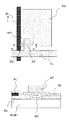
図10は、本発明による表示装置の画素の構成の他の実施例を示す平面図で、図2(a)に対応した図となっている。
<Example 2>
FIG. 10 is a plan view showing another embodiment of the pixel configuration of the display device according to the present invention and corresponds to FIG.
図10において、基板SUB1の表面の全域にわたって形成された第1透明酸化物層TOX1の面の区分された各領域に、ソース信号線SL、このソース信号線SLに接続される薄膜トランジスタTFT、この薄膜トランジスタTFTに接続される画素電極PXが形成されている。 In FIG. 10, a source signal line SL, a thin film transistor TFT connected to the source signal line SL, and a thin film transistor are provided in each divided region of the surface of the first transparent oxide layer TOX1 formed over the entire surface of the substrate SUB1. A pixel electrode PX connected to the TFT is formed.
図2(a)の場合と比較して異なる構成は、基板SUB1の表面に、ソース信号線SL、薄膜トランジスタTFT、画素電極PXの形成領域以外の領域においてもキャリア濃度の低い第1透明酸化物層(実効的に絶縁体として機能する)TOX1が形成されていることにある。すなわち、基板SUB1の表面の全域に形成された第1透明酸化物層TOX1は選択的にエッチングされていない構成となっている。 2A is different from the case of FIG. 2A in that the first transparent oxide layer having a low carrier concentration is formed on the surface of the substrate SUB1 even in a region other than the region where the source signal line SL, the thin film transistor TFT, and the pixel electrode PX are formed. That is, TOX1 (which effectively functions as an insulator) is formed. That is, the first transparent oxide layer TOX1 formed over the entire surface of the substrate SUB1 is not selectively etched.
このようにした場合であっても、ソース信号線SLと画素電極PXは第1透明酸化物層TOX1によって一体的にかつ同一層で形成されるため、それらの間隔(図中wで示す)を最小限に小さくでき、画素の開口率の向上を図った構成とすることができる。 Even in this case, since the source signal line SL and the pixel electrode PX are integrally formed in the same layer by the first transparent oxide layer TOX1, the distance between them (indicated by w in the figure) is set. It is possible to reduce the size to the minimum and to improve the pixel aperture ratio.
このように構成した第1透明酸化物層TOX1は、実施例1において図8、あるいは図9に示した製造方法において、第1フォトレジスト膜PRT1の形成の際に、通常どおりにフォトレジスト膜を形成すればよく、たとえばハーフ露光された段差のあるフォトレジスト膜を形成しなくてもよい効果を奏する。 The first transparent oxide layer TOX1 configured as described above is formed by applying a photoresist film as usual when the first photoresist film PRT1 is formed in the manufacturing method shown in FIG. For example, there is an effect that it is not necessary to form a half-exposed stepped photoresist film.
すなわち、たとえば図8(c)に示した工程に対応し、図10(a)のb−b線の個所における工程を示す図10(b)に示すように、第1フォトレジスト膜PRT1によって、薄膜トランジスタTFTのチャネル領域部CHおよびその両脇のLDD領域部LDを被うフォトレジスト膜、ソース信号線SL、薄膜トランジスタTFT、画素電極PXの形成領域以外の領域を被うフォトレジスト膜を形成し、その後は、図8に示した工程を経ればよいことになる。また、図9に示した製造方法を採用する場合においても同様である。 That is, for example, corresponding to the process shown in FIG. 8C, as shown in FIG. 10B showing the process at the line bb in FIG. 10A, the first photoresist film PRT1 Forming a photoresist film covering the channel region portion CH of the thin film transistor TFT and the LDD region portion LD on both sides thereof, a photoresist film covering the region other than the formation region of the source signal line SL, the thin film transistor TFT, and the pixel electrode PX; Thereafter, the process shown in FIG. The same applies to the case of employing the manufacturing method shown in FIG.
このような構成からなる表示装置は、液晶に面する表面における段差構造を少なくできるという効果を奏する。 The display device having such a configuration has an effect that the step structure on the surface facing the liquid crystal can be reduced.
〈実施例3〉
図11(a)は、本発明による表示装置の画素の構成の他の実施例を示す平面図で、図7、10(a)と対応した図である。また、図11(b)は図11(a)のb−b線における断面図である。
<Example 3>
FIG. 11A is a plan view showing another embodiment of the pixel configuration of the display device according to the present invention, and corresponds to FIGS. 7 and 10A. Moreover, FIG.11 (b) is sectional drawing in the bb line of Fig.11 (a).
図7、10(a)の場合と比較して異なる構成は、主となるソース信号線SL’が電気的抵抗の低いたとえば金属層で他の部材とは独立に形成されていることにある。 7 and 10 (a) is different in that the main source signal line SL 'is formed of a metal layer having a low electrical resistance, for example, independently of other members.
ここで、前記ソース信号線SL’を主と称したのは、該ソース信号線SL’にたとえば全域に及んで積層された第1透明酸化物層TOX1からなるソース信号線SLが形成されているからである。 Here, the source signal line SL ′ is mainly referred to as the source signal line SL formed of the first transparent oxide layer TOX1 stacked over the entire area of the source signal line SL ′, for example. Because.
すなわち、前記ソース信号線SL’が形成された基板SUB1の表面に図7、10に示した構成が積層され、図7、10に示したソース信号線SLが前記ソース信号線SL’に重畳して形成されるようになっている。 That is, the structure shown in FIGS. 7 and 10 is stacked on the surface of the substrate SUB1 on which the source signal line SL ′ is formed, and the source signal line SL shown in FIGS. 7 and 10 overlaps the source signal line SL ′. To be formed.
図7、10の場合の構成と比較し、第1透明酸化物層TOX1から構成されるソース信号線SLは、その下層に金属層から構成される前記ソース信号線SL’と接続して形成されることから、電気的抵抗を大幅に低減させることができる効果を奏する。 7 and 10, the source signal line SL composed of the first transparent oxide layer TOX1 is connected to the source signal line SL ′ composed of a metal layer in the lower layer. For this reason, the electrical resistance can be greatly reduced.
この場合、図11では、第1透明酸化物層TOX1からなるソース信号線SLと金属層からなるソース信号線SLは、それらの中心軸を一致づけてそれらの幅をほぼ同一としたものであるが、金属層からなるソース信号線SLの幅を第1透明酸化物層TOX1からなるソース信号線SLの幅よりも小さく構成するようにしてもよい。ソース信号線を全体として充分に電気的抵抗を低減させることができるからである。 In this case, in FIG. 11, the source signal line SL made of the first transparent oxide layer TOX1 and the source signal line SL made of the metal layer are made to have the same width by matching their central axes. However, the width of the source signal line SL made of the metal layer may be configured to be smaller than the width of the source signal line SL made of the first transparent oxide layer TOX1. This is because the electrical resistance of the source signal line can be sufficiently reduced as a whole.
図12は、前記ソース信号線SL’を基板SUB1の表面に形成する場合における製造方法の工程を示した工程図である。 FIG. 12 is a process diagram showing a process of the manufacturing method in the case where the source signal line SL 'is formed on the surface of the substrate SUB1.
図中の左側に描いた工程図は図11(a)のL−L線における断面図で示し、右側に描いた工程図は図11(a)のR−R線における断面図で示している。 The process drawing drawn on the left side of the drawing is shown by a cross-sectional view taken along line LL in FIG. 11A, and the process drawing drawn on the right side is shown by a cross-sectional view taken along line RR in FIG. .
図12(a)に示すように、基板SUB1の表面の全域に金属層MTを形成し、この金属層MTの表面においてパターン化されたフォトレジスト膜PRTをマスクとして該金属層MTを選択エッチングすることにより、前記ソース信号線SL’を形成する。 As shown in FIG. 12A, a metal layer MT is formed over the entire surface of the substrate SUB1, and the metal layer MT is selectively etched using the photoresist film PRT patterned on the surface of the metal layer MT as a mask. As a result, the source signal line SL ′ is formed.
次に、前記フォトレジスト膜PRTを除去した後に、図12(b)に示すように、たとえばZnOからなる第1透明酸化物層TOX1、および、たとえばSiO2からなる絶縁膜GIを順次積層させる。 Next, after removing the photoresist film PRT, as shown in FIG. 12B, a first transparent oxide layer TOX1 made of, for example, ZnO and an insulating film GI made of, for example, SiO2 are sequentially stacked.
この工程は、たとえば図8(a)に示す工程に相当し、その後、図8(b)〜図8(g)を経ることにより、図11に示した構成を完成させることができる。 This step corresponds to, for example, the step shown in FIG. 8A, and then the configuration shown in FIG. 11 can be completed by going through FIG. 8B to FIG. 8G.
上述した実施例では、ソース信号線SL’の全域にわたって第1透明酸化物層TOX1からなるソース信号線SLを積層させた構成としたものである。しかし、これに限定されることはなく、ソース信号線SL’の一部分にのみ前記ソース信号線SLを積層させる構成としてもよい。たとえば、薄膜トランジスタTFTの近傍におけるソース信号線SL’のみに前記ソース信号線SLを積層させる構成としてもよい。ソース信号線SL’は金属層で形成されていることから、それ自体で電気的抵抗を充分に低減させることができるからである。 In the embodiment described above, the source signal line SL made of the first transparent oxide layer TOX1 is laminated over the entire area of the source signal line SL '. However, the present invention is not limited to this, and the source signal line SL may be stacked only on a part of the source signal line SL '. For example, the source signal line SL may be stacked only on the source signal line SL ′ in the vicinity of the thin film transistor TFT. This is because the source signal line SL 'is formed of a metal layer, so that the electrical resistance can be sufficiently reduced by itself.
この場合、前記第1透明酸化物層TOX1および絶縁膜GIの順次積層体は、たとえば図13に示すパターンのようにして形成され、そのソース信号線SLとして形成される部分は薄膜トランジスタTFTの形成領域の近傍のみに止まって構成されている。 In this case, the sequential laminated body of the first transparent oxide layer TOX1 and the insulating film GI is formed, for example, in the pattern shown in FIG. 13, and the portion formed as the source signal line SL is a formation region of the thin film transistor TFT. It is configured to stop only in the vicinity.
〈実施例4〉
図14(a)は、本発明による表示装置の画素の構成の他の実施例を示す平面図で、図11(a)と対応した図である。また、図14(b)は図14(a)のb−b線における断面図である。
<Example 4>
FIG. 14A is a plan view showing another embodiment of the configuration of the pixel of the display device according to the present invention and corresponds to FIG. 11A. FIG. 14B is a cross-sectional view taken along line bb in FIG.
図11(a)の場合と比較し、同様に主たるソース信号線SL’を有するが、該ソース信号線SL’は前記ソース信号線SLの上層に配置されていることが図11(a)の場合と異なっている。 Compared to the case of FIG. 11A, the main source signal line SL ′ is similarly provided, but the source signal line SL ′ is disposed in the upper layer of the source signal line SL of FIG. It is different from the case.
この場合においてもソース信号線SL’は、たとえば金属層で形成され、また第1透明酸化物層TOX1からなるソース信号線SLと積層されて形成されていることから、電気的抵抗を大幅に低減させることができる。 Also in this case, since the source signal line SL ′ is formed of, for example, a metal layer and is stacked with the source signal line SL made of the first transparent oxide layer TOX1, the electrical resistance is greatly reduced. Can be made.
また、図14では、第1透明酸化物層TOX1からなるソース信号線SLと金属層からなるソース信号線SLは、それらの中心軸を一致づけてそれらの幅をほぼ同一としたものであるが、金属層からなるソース信号線SLの幅を第1透明酸化物層TOX1からなるソース信号線SLの幅よりも小さく構成するようにしてもよい。ソース信号線を全体として充分に電気的抵抗を低減させることができるからである。 Further, in FIG. 14, the source signal line SL made of the first transparent oxide layer TOX1 and the source signal line SL made of the metal layer are made the same in width by matching their central axes. The width of the source signal line SL made of the metal layer may be made smaller than the width of the source signal line SL made of the first transparent oxide layer TOX1. This is because the electrical resistance of the source signal line can be sufficiently reduced as a whole.
図15は、前記表示装置の画素の製造方法の一実施例を示す工程図であり、図中左側の工程図は図14(a)のL−L線における断面図で示し、図中右側の工程図は図14(a)のR−R線における断面図で示している。 FIG. 15 is a process diagram showing an embodiment of a method for manufacturing a pixel of the display device. The process diagram on the left side of the figure is shown by a cross-sectional view taken along line LL in FIG. The process diagram is shown by a cross-sectional view taken along line RR in FIG.
以下、工程順に説明する。 Hereinafter, it demonstrates in order of a process.
工程1.
図15(a)に示すように、基板SUB1を用意し、この基板SUB1の表面にたとえばZnO等からなる高抵抗の第1透明酸化物層TOX1およびたとえばSiO2等からなる第1絶縁膜GI1を順次成膜する。
Step 1.
As shown in FIG. 15 (a), providing a substrate SUB1, a first insulating film GI1 made of the first transparent oxide layer TOX1 and for example, SiO 2 of high resistance on the surface of the substrate SUB1 made of, for example, ZnO or the like Films are sequentially formed.
工程2.
図15(b)に示すように、前記第1絶縁膜GI1の上面の全域に第1フォトレジスト膜PRT1を形成し、この第1フォトレジスト膜PRT1を所定のパターンに形成する。
Step 2.
As shown in FIG. 15B, a first photoresist film PRT1 is formed over the entire upper surface of the first insulating film GI1, and the first photoresist film PRT1 is formed in a predetermined pattern.
ここで、パターン化された第1フォトレジスト膜PRT1は、図14(a)に示す画素のうち、ソース信号線SL、このソース信号線SLと接続される薄膜トランジスタTFT、この薄膜トランジスタTFTと接続される画素電極PXの各形成領域に形成され、かつ、前記薄膜トランジスタTFTのチャネル領域部およびその両脇のLDD領域部の形成領域において高くそれ以外の部分が低いというように二段の高低を有するようにして形成されている。 Here, the patterned first photoresist film PRT1 is connected to the source signal line SL, the thin film transistor TFT connected to the source signal line SL, and the thin film transistor TFT in the pixel shown in FIG. It is formed in each formation region of the pixel electrode PX, and has a two-step height such that the channel region portion of the thin film transistor TFT and the formation region of the LDD region portion on both sides thereof are high and the other portions are low. Is formed.
そして、前記第1フォトレジスト膜PRT1をマスクとし、このマスクから露出された第1絶縁膜GI1およびこの第1絶縁膜GI1の下層の第1透明酸化物層TOX1を順次エッチングし、基板SUB1の表面を露出させる。 Then, using the first photoresist film PRT1 as a mask, the first insulating film GI1 exposed from the mask and the first transparent oxide layer TOX1 under the first insulating film GI1 are sequentially etched, and the surface of the substrate SUB1 To expose.
このようにして第1透明酸化物層TOX1と第1絶縁膜GI1の積層体は、ソース信号線SL、このソース信号線SLと接続される薄膜トランジスタTFT、この薄膜トランジスタTFTと接続される画素電極PXの形成領域に残存される。 Thus, the stacked body of the first transparent oxide layer TOX1 and the first insulating film GI1 includes the source signal line SL, the thin film transistor TFT connected to the source signal line SL, and the pixel electrode PX connected to the thin film transistor TFT. It remains in the formation area.
工程3.
図15(c)に示すように、前記第1フォトレジスト膜PRT1の表面を底面方向に適当量の除去を行うことによって、該第1フォトレジスト膜PRT1を、薄膜トランジスタTFTのチャネル領域部およびその両脇のLDD領域部の形成領域にのみ残存させるようにする。
Step 3.
As shown in FIG. 15C, by removing an appropriate amount of the surface of the first photoresist film PRT1 in the bottom direction, the first photoresist film PRT1 is removed from the channel region portion of the thin film transistor TFT and both of them. It is made to remain only in the formation region of the side LDD region.
そして、第1絶縁膜GI1を通して第1透明酸化物層TOX1にレーザ光RLを照射することによって該第1透明酸化物層TOX1に結晶改質を行いキャリア濃度を向上させる。この場合、前記第1フォトレジスト膜TOX1が形成されている部分においてレーザ光RLの照射が阻止され該第1フォトレジスト膜PRT1の直下の第1透明酸化物層TOX1は高抵抗が維持される。 Then, by irradiating the first transparent oxide layer TOX1 with the laser light RL through the first insulating film GI1, the first transparent oxide layer TOX1 is crystal-modified to improve the carrier concentration. In this case, irradiation of the laser beam RL is blocked at the portion where the first photoresist film TOX1 is formed, and the first transparent oxide layer TOX1 directly below the first photoresist film PRT1 maintains a high resistance.
工程4.
図15(d)に示すように、前記第1フォトレジスト膜PRT1を全て除去する。
Step 4.
As shown in FIG. 15D, the first photoresist film PRT1 is completely removed.
工程5.
図15(e)に示すように、基板SUB1の表面に第2フォトレジスト膜PRT2を形成し、該第2フォトレジスト膜PRT2をパターン化することによって、ソース信号線SLを形成する部分において除去され他の部分において残存される第2フォトレジスト膜PRT2を形成する。
Step 5.
As shown in FIG. 15E, the second photoresist film PRT2 is formed on the surface of the substrate SUB1, and the second photoresist film PRT2 is patterned to be removed in a portion where the source signal line SL is formed. A second photoresist film PRT2 remaining in other portions is formed.
そして、該第2フォトレジスト膜PRT2から露出する前記第1絶縁膜GI1を選択エッチングし、前記第1透明酸化物層TOX1の結晶改質がなされた部分(ソース信号線SLの部分)を露呈させる。 Then, the first insulating film GI1 exposed from the second photoresist film PRT2 is selectively etched to expose a portion of the first transparent oxide layer TOX1 that has undergone crystal modification (a portion of the source signal line SL). .
さらに、前記第2フォトレジスト膜PRT2をそのまま残存させ、その上方から金属を蒸着させ、該第2フォトレジスト膜PRT2を剥離させる。いわゆるリフトオフ法と称され、前記第1透明酸化物層TOX1の結晶改質がなされた部分(ソース信号線SLの部分)に金属層MTが形成されることになる。この金属層MTはソース信号線SLに積層して形成されるソース信号線SL’に相当するものとなる。 Further, the second photoresist film PRT2 is left as it is, a metal is deposited from above, and the second photoresist film PRT2 is peeled off. This is referred to as a so-called lift-off method, and the metal layer MT is formed in a portion where the crystal modification of the first transparent oxide layer TOX1 is performed (portion of the source signal line SL). The metal layer MT corresponds to the source signal line SL ′ formed by being stacked on the source signal line SL.
工程6.
図15(f)に示すように、前記第2フォトレジスト膜PRT2を除去し、たとえばSiO2からなる第2絶縁膜GI2およびたとえばITO膜からなる第2透明酸化物層TOX2を順次形成する。
Step 6.
As shown in FIG. 15F, the second photoresist film PRT2 is removed, and a second insulating film GI2 made of, for example, SiO 2 and a second transparent oxide layer TOX2 made of, for example, an ITO film are sequentially formed.
工程7.
図15(g)に示すように、基板SUB1の表面に第3フォトレジスト膜PRT3を形成し、該第3フォトレジスト膜PRT3をパターン化することによって、ゲート信号線GLおよび薄膜トランジスタTFTのゲート電極GTを形成する部分において残存される第3フォトレジスト膜PRT3を形成する。
Step 7.
As shown in FIG. 15G, a third photoresist film PRT3 is formed on the surface of the substrate SUB1, and the third photoresist film PRT3 is patterned, whereby the gate signal line GL and the gate electrode GT of the thin film transistor TFT are formed. A third photoresist film PRT3 remaining in the portion where the film is formed is formed.
そして、第3フォトレジスト膜PRT3をマスクとし、このマスクから露出する前記第2透明酸化物層TOX2を選択エッチングし、その下層の第2絶縁膜GI2を露呈させる。 Then, using the third photoresist film PRT3 as a mask, the second transparent oxide layer TOX2 exposed from the mask is selectively etched to expose the underlying second insulating film GI2.
さらに、前記第3フォトレジスト膜PRT3をそのまま残存させ、前記第2絶縁膜GI2を通して第1透明酸化物層TOX1にレーザ光RLを照射する。これにより、ゲート電極GTの直下の薄膜トランジスタTFTのチャネル領域部と前記ソース信号線SL’との間の領域において結晶改質がなされLDD領域部LDが形成される。このため、この工程におけるレーザ光RLによる結晶改質は、前記工程3におけるレーザ光RLによる結晶改質よりも、その改質程度を小さくする必要がある。 Further, the third photoresist film PRT3 is left as it is, and the first transparent oxide layer TOX1 is irradiated with the laser light RL through the second insulating film GI2. As a result, crystal modification is performed in a region between the channel region portion of the thin film transistor TFT and the source signal line SL 'immediately below the gate electrode GT, thereby forming an LDD region portion LD. For this reason, the crystal modification by the laser beam RL in this step needs to be smaller than the crystal modification by the laser beam RL in the step 3.
工程8.
図15(h)に示すように、前記第3フォトレジスト膜PRT3を除去する。
Step 8.
As shown in FIG. 15H, the third photoresist film PRT3 is removed.
図16は、前記表示装置の画素の製造方法の他の実施例を示す工程図であり、図中左側の工程図は図14(a)のL−L線における断面図で示し、図中右側の工程図は図14(a)のR−R線における断面図で示している。 FIG. 16 is a process diagram showing another embodiment of a method for manufacturing a pixel of the display device, and the process diagram on the left side in the figure is shown by a cross-sectional view taken along line LL in FIG. FIG. 14A is a sectional view taken along line RR in FIG.
以下、工程順に説明する。 Hereinafter, it demonstrates in order of a process.
工程1.
図16(a)に示すように、基板SUB1を用意し、この基板SUB1の表面にたとえばZnO等からなる高抵抗の第1透明酸化物層TOX1およびたとえばSiO2等からなる第1絶縁膜GI1を順次成膜する。
Step 1.
As shown in FIG. 16 (a), providing a substrate SUB1, a first insulating film GI1 made of the first transparent oxide layer TOX1 and for example, SiO 2 of high resistance on the surface of the substrate SUB1 made of, for example, ZnO or the like Films are sequentially formed.
工程2.
図16(b)に示すように、前記第1絶縁膜GI1の上面の全域に第1フォトレジスト膜PRT1を形成し、この第1フォトレジスト膜PRT1を所定のパターンに形成する。
Step 2.
As shown in FIG. 16B, a first photoresist film PRT1 is formed over the entire upper surface of the first insulating film GI1, and the first photoresist film PRT1 is formed in a predetermined pattern.
ここで、パターン化された第1フォトレジスト膜PRT1は、図14(a)に示す画素のうち、ソース信号線SL、このソース信号線SLと接続される薄膜トランジスタTFT、この薄膜トランジスタTFTと接続される画素電極PXの各形成領域に形成され、かつ、前記薄膜トランジスタTFTのチャネル領域部およびその両脇のLDD領域部の形成領域において高くそれ以外の部分が低いというように二段の高低を有するようにして形成されている。 Here, the patterned first photoresist film PRT1 is connected to the source signal line SL, the thin film transistor TFT connected to the source signal line SL, and the thin film transistor TFT in the pixel shown in FIG. It is formed in each formation region of the pixel electrode PX, and has a two-step height such that the channel region portion of the thin film transistor TFT and the formation region of the LDD region portion on both sides thereof are high and the other portions are low. Is formed.
そして、前記第1フォトレジスト膜PRT1をマスクとし、このマスクから露出された第1絶縁膜GI1およびこの第1絶縁膜GI1の下層の第1透明酸化物層TOX1を順次エッチングし、基板SUB1の表面を露出させる。 Then, using the first photoresist film PRT1 as a mask, the first insulating film GI1 exposed from the mask and the first transparent oxide layer TOX1 under the first insulating film GI1 are sequentially etched, and the surface of the substrate SUB1 To expose.
このようにして第1透明酸化物層TOX1と第1絶縁膜GI1の積層体は、ソース信号線SL、このソース信号線SLと接続される薄膜トランジスタTFT、この薄膜トランジスタTFTと接続される画素電極PXの部分に残存される。 Thus, the stacked body of the first transparent oxide layer TOX1 and the first insulating film GI1 includes the source signal line SL, the thin film transistor TFT connected to the source signal line SL, and the pixel electrode PX connected to the thin film transistor TFT. It remains in the part.
工程3.
図16(c)に示すように、前記第1フォトレジスト膜PRT1の表面を底面方向に適当量の除去を行うことによって、該第1フォトレジスト膜PRT1を、薄膜トランジスタTFTのチャネル領域部およびその両脇のLDD領域部の形成領域にのみ残存させるようにする。
Step 3.
As shown in FIG. 16C, by removing an appropriate amount of the surface of the first photoresist film PRT1 in the bottom direction, the first photoresist film PRT1 is removed from the channel region portion of the thin film transistor TFT and both of them. It is made to remain only in the formation region of the side LDD region.
そして、第1絶縁膜GI1を通して第1透明酸化物層TOX1にレーザ光RLを照射することによって該第1透明酸化物層TOX1に結晶改質を行いキャリア濃度を向上させる。この場合、前記第1フォトレジスト膜PRT1が形成されている部分においてレーザ光RLの照射が阻止され該第1フォトレジスト膜PRT1の直下の第1透明酸化物層TOX1は高抵抗が維持される。 Then, by irradiating the first transparent oxide layer TOX1 with the laser light RL through the first insulating film GI1, the first transparent oxide layer TOX1 is crystal-modified to improve the carrier concentration. In this case, the irradiation with the laser beam RL is blocked at the portion where the first photoresist film PRT1 is formed, and the first transparent oxide layer TOX1 immediately below the first photoresist film PRT1 maintains a high resistance.
その後、さらに前記第1フォトレジスト膜PRT1をマスクとして、前記第1絶縁膜GI1を除去する。 Thereafter, the first insulating film GI1 is further removed using the first photoresist film PRT1 as a mask.
工程4.
図16(d)に示すように、基板SUB1の表面の全域に金属を蒸着し、金属層MTを形成する。
Step 4.
As shown in FIG. 16D, metal is deposited on the entire surface of the substrate SUB1 to form a metal layer MT.
工程5.
図16(e)に示すように、基板SUB1の表面の全域に第2フォトレジスト膜PRT2を形成し、この第2フォトレジスト膜PRT2をパターン化して、ソース信号線SLの形成領域に第2フォトレジスト膜PRT2を残存させる。
Step 5.
As shown in FIG. 16E, a second photoresist film PRT2 is formed over the entire surface of the substrate SUB1, and this second photoresist film PRT2 is patterned to form the second photo film in the formation region of the source signal line SL. The resist film PRT2 is left.
そして、この第2フォトレジスト膜PRT2をマスクとし、このマスクから露出された前記金属層MTを選択エッチングする。 Then, using the second photoresist film PRT2 as a mask, the metal layer MT exposed from the mask is selectively etched.
さらに、前記第2フォトレジスト膜PRT2を除去し、残存された前記金属層MTをソース信号線SL’として構成する。 Further, the second photoresist film PRT2 is removed, and the remaining metal layer MT is configured as a source signal line SL '.
工程6.
図16(f)に示すように、たとえばSiO2からなる第2絶縁膜GI2およびたとえばITO膜からなる第2透明酸化物層TOX2を順次形成する。
Step 6.
As shown in FIG. 16F, a second insulating film GI2 made of, for example, SiO 2 and a second transparent oxide layer TOX2 made of, for example, an ITO film are sequentially formed.
工程7.
図16(g)に示すように、基板SUB1の表面に第3フォトレジスト膜PRT3を形成し、該第3フォトレジスト膜PRT3をパターン化することによって、ゲート信号線GLおよび薄膜トランジスタTFTのゲート電極GTを形成する部分において残存される第3フォトレジスト膜PRT3を形成する。
Step 7.
As shown in FIG. 16G, a third photoresist film PRT3 is formed on the surface of the substrate SUB1, and the third photoresist film PRT3 is patterned, whereby the gate signal line GL and the gate electrode GT of the thin film transistor TFT are formed. A third photoresist film PRT3 remaining in the portion where the film is formed is formed.
そして、第3フォトレジスト膜PRT3をマスクとし、このマスクから露出する前記第2透明酸化物層TOX2を選択エッチングし、その下層の第2絶縁膜GI2を露呈させる。 Then, using the third photoresist film PRT3 as a mask, the second transparent oxide layer TOX2 exposed from the mask is selectively etched to expose the underlying second insulating film GI2.
さらに、前記第3フォトレジスト膜PRT3をそのまま残存させ、前記第2絶縁膜GI2を通して第1透明酸化物層TOX1にレーザ光RLを照射する。これにより、ゲート電極GTの直下の薄膜トランジスタTFTのチャネル領域部と前記ソース信号線SL’との間の領域において結晶改質がなされLDD領域部LDが形成される。このため、この工程におけるレーザ光LDによる結晶改質は、前記工程3におけるレーザ光LDによる結晶改質よりも、その改質程度を小さくする必要がある。 Further, the third photoresist film PRT3 is left as it is, and the first transparent oxide layer TOX1 is irradiated with the laser light RL through the second insulating film GI2. As a result, crystal modification is performed in a region between the channel region portion of the thin film transistor TFT and the source signal line SL 'immediately below the gate electrode GT, thereby forming an LDD region portion LD. For this reason, the crystal modification by the laser beam LD in this step needs to be made smaller than the crystal modification by the laser beam LD in the step 3.
工程8.
図16(h)に示すように、前記第3フォトレジスト膜PRT3を除去する。
Step 8.
As shown in FIG. 16H, the third photoresist film PRT3 is removed.
〈実施例5〉
図17(a)は、本発明による表示装置の画素の構成の他の実施例を示す平面図である。また、図17(b)は、図17(a)のb−b線における断面図である。
<Example 5>
FIG. 17A is a plan view showing another embodiment of the pixel configuration of the display device according to the present invention. Moreover, FIG.17 (b) is sectional drawing in the bb line of Fig.17 (a).
図17に示す画素は、基板SUB1の液晶側の画素領域において画素電極PXとこの画素電極PXとの間で電界を生じせしめる対向電極CTを有するように構成されている。 The pixel shown in FIG. 17 is configured to have a pixel electrode PX and a counter electrode CT that generates an electric field between the pixel electrode PX in the pixel region on the liquid crystal side of the substrate SUB1.
画素電極PXは薄膜トランジスタTFTを介してソース信号線SLから映像信号が供給される構成となっており、上述した実施例に示した構成とほぼ同じとなっている。 The pixel electrode PX has a configuration in which a video signal is supplied from the source signal line SL via the thin film transistor TFT, and is substantially the same as the configuration shown in the above-described embodiment.
前記対向電極CTは、前記画素電極PXに絶縁膜(たとえば第1絶縁膜)を介し該画素電極PXと重畳して配置されるとともに、並設された多数の電極からなる櫛歯状電極として構成されている。 The counter electrode CT is arranged as a comb-like electrode composed of a large number of electrodes arranged in parallel with the pixel electrode PX so as to overlap the pixel electrode PX via an insulating film (for example, a first insulating film). Has been.
なお、この対向電極CTはその各電極の中途部において前記ゲート信号線GLとほぼ平行に走行するコモン信号線CLと一体となって形成され、該コモン信号線CLを通して映像信号に対して基準となる基準電圧が前記櫛歯状電極に印加されるようになっている。 The counter electrode CT is formed integrally with a common signal line CL that runs substantially in parallel with the gate signal line GL in the middle part of each electrode, and is used as a reference for the video signal through the common signal line CL. The reference voltage is applied to the comb-like electrode.
また、前記コモン信号線CLと一体の櫛歯状電極は前記ゲート信号線GLと同層となっており、たとえば該ゲート信号線GLの形成の際に同時に形成されるようになっている。 Further, the comb-like electrode integrated with the common signal line CL is in the same layer as the gate signal line GL, and is formed simultaneously with the formation of the gate signal line GL, for example.
このように構成された画素に図示しない配向膜を介して配置される液晶の分子は前記画素電極PXと対向電極CTの間に発生する電界によって挙動するようになっている。 The liquid crystal molecules arranged in the pixel configured as described above via an alignment film (not shown) behaves by an electric field generated between the pixel electrode PX and the counter electrode CT.
そして、この場合における画素の構成は、その画素電極PXにおいてその全域にわたって結晶改質(あるいは不純物ドーピング)がなされて導体化されたものとなっている。 The pixel configuration in this case is a conductor formed by crystal modification (or impurity doping) over the entire region of the pixel electrode PX.
その製造において、たとえば実施例1の図8に示したような方法を用い、ソース信号線SLにおける結晶改質(あるいは不純物ドーピング)と同時に画素電極PXの結晶改質(あるいは不純物ドーピング)をした場合は、画素電極はその全域にわたって結晶改質(あるいは不純物ドーピング)がなされる。 In the manufacture, for example, the method as shown in FIG. 8 of the first embodiment is used, and the crystal modification (or impurity doping) of the pixel electrode PX is performed simultaneously with the crystal modification (or impurity doping) in the source signal line SL. The crystal modification (or impurity doping) is performed on the entire area of the pixel electrode.
しかし、このような構成に限定されることはなく、たとえば、図17(b)に対応する図18に示すように、画素電極PXの前記対向電極CTの直下における領域において結晶改質がなされていない場合であってもよい。画素の製造において、たとえば実施例1の図9に示したような方法を用いた場合、画素電極PXへのレーザ光RLの照射(あるいは不純物ドーピング)の際に既に形成されている対向電極CTがマスクとなり、図18に示すような構成となる。 However, the present invention is not limited to such a configuration. For example, as shown in FIG. 18 corresponding to FIG. 17B, crystal modification is performed in a region immediately below the counter electrode CT of the pixel electrode PX. There may be no case. In manufacturing the pixel, for example, when the method as shown in FIG. 9 of the first embodiment is used, the counter electrode CT already formed when the pixel electrode PX is irradiated with the laser light RL (or impurity doping) is formed. A mask is formed as shown in FIG.
なお、この場合にあって、画素電極PXはコモン信号線CLの下方においてもキャリア濃度が低くなってしまい、画素電極PX内に電位が到達し難いという不都合を解消したい場合が生じる。 In this case, there is a case where the pixel electrode PX has a low carrier concentration even below the common signal line CL, and the inconvenience that it is difficult for the potential to reach the pixel electrode PX occurs.
この場合、図19に示すように、対向電極CTと一体化して形成するコモン信号線CLを画素領域の周辺側に位置づけるように、すなわち、対向電極CTの一端部において該コモン信号線CLを結合させるパターンとして形成することによって、画素電極PXの有効利用が図れるようになる。 In this case, as shown in FIG. 19, the common signal line CL formed integrally with the counter electrode CT is positioned on the peripheral side of the pixel region, that is, the common signal line CL is coupled at one end of the counter electrode CT. By forming the pattern to be used, the pixel electrode PX can be effectively used.
〈実施例6〉
図20(a)は、本発明による表示装置の画素の構成の他の実施例を示す平面図であり、基板SUB1の面に形成する2つの各透明酸化物層のうち上層に形成される第2透明酸化物層TOX2が画素の領域の全域に形成され、その一部にゲート信号線GLおよびゲート電極GTが形成されていることを示した図となっている。また、図20(b)は、図20(a)のb−b線における断面図である。
<Example 6>
FIG. 20A is a plan view showing another embodiment of the configuration of the pixel of the display device according to the present invention, in which the first of the two transparent oxide layers formed on the surface of the substrate SUB1 is formed in the upper layer. 2 shows that two transparent oxide layers TOX2 are formed in the entire region of the pixel, and a gate signal line GL and a gate electrode GT are formed in a part thereof. FIG. 20B is a cross-sectional view taken along the line bb in FIG.
基板SUB1の面に形成する2つの各透明酸化物層TOX1、TOX2のうち、下層に形成される第1透明酸化物層TOX1は、画素の領域の全域に形成され、その一部にソース信号線SL、このソース信号線SLに接続される薄膜トランジスタTFT、この薄膜トランジスタTFTに接続される画素電極PXが形成されている。 Of the two transparent oxide layers TOX1 and TOX2 formed on the surface of the substrate SUB1, the first transparent oxide layer TOX1 formed in the lower layer is formed in the entire region of the pixel, and a source signal line is formed in a part thereof. SL, a thin film transistor TFT connected to the source signal line SL, and a pixel electrode PX connected to the thin film transistor TFT are formed.
この第1透明酸化物層TOX1において、前記ソース信号線SL、薄膜トランジスタTFT、画素電極PX以外の領域にあっては結晶改質(あるいは不純物ドーピング)がなされていない領域(絶縁領域)となっている。このことから、この第1透明酸化物層TOX1は段差が形成されていない平坦な層として構成されている。 In the first transparent oxide layer TOX1, the region other than the source signal line SL, the thin film transistor TFT, and the pixel electrode PX is a region (insulating region) that is not subjected to crystal modification (or impurity doping). . From this, this 1st transparent oxide layer TOX1 is comprised as a flat layer in which the level | step difference is not formed.
また、この第1透明酸化物層TOX1の上面には絶縁膜GIを介して第2透明酸化物層TOX2が画素の領域の全域に形成され、その一部にゲート信号線GLおよびこのゲート信号線GLに接続されたゲート電極GTが形成されている。すなわち、この第2透明酸化物層TOX2において、前記ゲート信号線GL、ゲート電極GT以外の領域にあっては結晶改質(あるいは不純物ドーピング)がなされておらず充分な透明性が確保された領域となっている。したがって、この第2透明酸化物層TOX2にあっても段差が形成されていない平坦な層として構成される。 Further, a second transparent oxide layer TOX2 is formed on the entire upper surface of the first transparent oxide layer TOX1 via an insulating film GI, and a gate signal line GL and the gate signal line are formed in a part of the second transparent oxide layer TOX2. A gate electrode GT connected to the GL is formed. In other words, in the second transparent oxide layer TOX2, the region other than the gate signal line GL and the gate electrode GT is not subjected to crystal modification (or impurity doping) and has sufficient transparency. It has become. Therefore, even if it exists in this 2nd transparent oxide layer TOX2, it is comprised as a flat layer in which the level | step difference is not formed.
このように構成した表示装置は、画素の領域の全域に形成された第1透明酸化物層TOX1、絶縁膜GI、第2透明酸化物層TOX2の順次積層体によって、ソース信号線SL、ゲート信号線GL、薄膜トランジスタTFT、画素電極PXを形成できることから、表面における段差の発生を回避できる構成とすることができる。 In the display device configured as described above, the source signal line SL and the gate signal are formed by sequentially stacking the first transparent oxide layer TOX1, the insulating film GI, and the second transparent oxide layer TOX2 formed over the entire pixel region. Since the line GL, the thin film transistor TFT, and the pixel electrode PX can be formed, it is possible to avoid the occurrence of a step on the surface.
また、図21は、本発明による表示装置の画素の構成の他の実施例を示す平面図であり、図20(a)に対応した図となっている。 FIG. 21 is a plan view showing another embodiment of the configuration of the pixel of the display device according to the present invention, and corresponds to FIG.
図21は、基板SUB1に対向電極CTおよびこの対向電極CTと接続されるコモン信号線CLを備えるものを示し、これら対向電極CTおよびコモン信号線CLは図20(a)に示した第2透明酸化物層TOX2の一部に形成されるようになっている。 FIG. 21 shows a substrate SUB1 provided with a counter electrode CT and a common signal line CL connected to the counter electrode CT. These counter electrode CT and common signal line CL are the second transparent shown in FIG. It is formed on a part of the oxide layer TOX2.
基板SUB1の表面に形成された第2透明酸化物層TOX2に選択的に結晶改質(あるいは不純物ドーピング)を行って、ゲート信号線GL、ゲート電極GTとともに、前記対向電極CT、コモン信号線CLを形成するようになっている。 The second transparent oxide layer TOX2 formed on the surface of the substrate SUB1 is selectively subjected to crystal modification (or impurity doping), and together with the gate signal line GL and the gate electrode GT, the counter electrode CT and the common signal line CL. Is supposed to form.
このように構成した表示装置においても、基板SUB1の表面における段差の発生を回避できる構成とすることができる。 Even in the display device configured as described above, it is possible to avoid the occurrence of a step on the surface of the substrate SUB1.
〈実施例7〉
図22は基板SUB1の表面にアレイ状に配置された各画素の一実施例を示した平面図で、図1と対応した図である。
<Example 7>
FIG. 22 is a plan view showing one embodiment of each pixel arranged in an array on the surface of the substrate SUB1, and corresponds to FIG.
図1の場合と比較して異なる構成は、薄膜トランジスタTFTにあり、その半導体層SCがたとえばゲート電極GTの両脇からはみ出して形成されている。この半導体層SCは、ソース信号線SLおよび画素電極PX等を構成する第1透明酸化物層TOX1と別個に形成されるものとして構成されている。 A configuration different from that in FIG. 1 is in the thin film transistor TFT, and the semiconductor layer SC is formed so as to protrude from both sides of the gate electrode GT, for example. The semiconductor layer SC is configured to be formed separately from the first transparent oxide layer TOX1 constituting the source signal line SL, the pixel electrode PX, and the like.
図23(a)は、前記各画素のうちの一画素を抜き出し拡大して示した図であり、そのb−b線における断面図を図23(b)に示している。 FIG. 23A is a diagram showing one of the pixels extracted and enlarged, and FIG. 23B shows a cross-sectional view taken along the line bb.
図23(b)において、基板SUB1の表面に薄膜トランジスタTFTのソース領域部STとドレイン領域部DTが物理的に離間されて配置されている。 In FIG. 23B, the source region ST and the drain region DT of the thin film transistor TFT are physically separated on the surface of the substrate SUB1.
前記ソース領域部STはソース信号線SLの延在部として前記ドレイン領域部DTは画素電極PXの延在部として形成され、これらはいずれもたとえば不純物がドープされたZnOやITO等の透明導電膜からなる第1透明酸化物層TOX1によって形成されている。 The source region ST is formed as an extension of the source signal line SL, and the drain region DT is formed as an extension of the pixel electrode PX, both of which are, for example, transparent conductive films such as ZnO or ITO doped with impurities. The first transparent oxide layer TOX1 is made of.
すなわち、前記第1透明酸化物層TOX1は、ソース信号線SL、このソース信号線SLの延在部としての薄膜トランジスタTFTのソース領域部ST、画素電極PX、この画素電極PXの延在部としての薄膜トランジスタTFTのドレイン領域部の各形成領域に形成され、さらに、薄膜トランジスタTFTのチャネル領域部に切り欠き部が形成されたパターンとして構成されている。 That is, the first transparent oxide layer TOX1 includes the source signal line SL, the source region ST of the thin film transistor TFT as the extension of the source signal line SL, the pixel electrode PX, and the extension of the pixel electrode PX. The pattern is formed in each formation region of the drain region of the thin film transistor TFT and further has a notch formed in the channel region of the thin film transistor TFT.
そして、前記ソース領域部STとドレイン領域部DTの間には、半導体層SCがその一端において前記ソース領域部STと重畳し他端において前記ドレイン領域部DTと重畳して配置されている。ソース領域部STとドレイン領域部DTとの間にある前記半導体層SCは薄膜トランジスタTFTのチャネル領域部CHとして機能するようになっている。 Between the source region ST and the drain region DT, the semiconductor layer SC is disposed so as to overlap the source region ST at one end and to overlap the drain region DT at the other end. The semiconductor layer SC between the source region ST and the drain region DT functions as a channel region CH of the thin film transistor TFT.
このように形成された基板SUB1の表面には前記ソース信号線SL、ソース領域部ST、半導体層SC、ドレイン領域部DT、画素電極PX等を被って絶縁膜GIが形成され、この絶縁膜GIの上面に前記半導体層SCのチャネル領域に重畳してゲート電極GTが形成されている。このゲート電極GTはゲート信号線GLの延在部として構成されている。 An insulating film GI is formed on the surface of the substrate SUB1 formed in this manner so as to cover the source signal line SL, the source region ST, the semiconductor layer SC, the drain region DT, the pixel electrode PX, and the like. A gate electrode GT is formed on the upper surface of the semiconductor layer SC so as to overlap the channel region of the semiconductor layer SC. The gate electrode GT is configured as an extension of the gate signal line GL.
図25は、前記表示装置の製造方法の一実施例を示す工程図である。 FIG. 25 is a process diagram showing an embodiment of a method for manufacturing the display device.
ここで、図25に示す工程は液晶表示領域の一画素における工程図を示し、図25の左側に示す工程図は図23に示す画素の図中L−Lの個所に相当し、図25の右側に示す工程図は図23に示す画素の図中R−Rの個所に相当している。なお、図24に示す画素は図23(a)に示した画素と同様となっている。 Here, the process shown in FIG. 25 is a process diagram in one pixel of the liquid crystal display region, and the process diagram shown on the left side of FIG. 25 corresponds to the portion LL in the diagram of the pixel shown in FIG. The process chart shown on the right side corresponds to the RR portion of the pixel shown in FIG. Note that the pixel shown in FIG. 24 is the same as the pixel shown in FIG.
以下、工程順に説明する。 Hereinafter, it demonstrates in order of a process.
工程1.
図25(a)に示すように、基板SUB1を用意し、この基板SUB1の表面にたとえば不純物がドープされたZnOからなる第1透明酸化物層TOX1を形成する。
Step 1.
As shown in FIG. 25A, a substrate SUB1 is prepared, and a first transparent oxide layer TOX1 made of, for example, ZnO doped with impurities is formed on the surface of the substrate SUB1.
工程2.
図25(b)に示すように、基板SUB1の表面に第1フォトレジスト膜PRT1を形成し、これをパターン化することにより、ソース信号線SL、このソース信号線SLの延在部となる薄膜トランジスタTFTのソース領域部ST、画素電極PX、この画素電極PXの延在部となる薄膜トランジスタTFTのドレイン領域部DTの形成領域における第1フォトレジスト膜PRT1を残存させる。
Step 2.
As shown in FIG. 25B, a first photoresist film PRT1 is formed on the surface of the substrate SUB1, and this is patterned to form a source signal line SL and a thin film transistor that becomes an extension portion of the source signal line SL. The first photoresist film PRT1 in the formation region of the source region ST of the TFT, the pixel electrode PX, and the drain region DT of the thin film transistor TFT serving as the extension of the pixel electrode PX is left.
そして、残存された第1フォトレジスト膜PRT1をマスクとし、このマスクから露出された第1透明酸化物層TOX1を選択エッチングする。これにより、ソース信号線SL、薄膜トランジスタTFTのソース領域部ST、画素電極PX、薄膜トランジスタTFTのドレイン領域部DTが形成される。 Then, using the remaining first photoresist film PRT1 as a mask, the first transparent oxide layer TOX1 exposed from the mask is selectively etched. Thus, the source signal line SL, the source region ST of the thin film transistor TFT, the pixel electrode PX, and the drain region DT of the thin film transistor TFT are formed.
工程3.
図25(c)に示すように、前記第1フォトレジスト膜PRT1を除去する。
Step 3.
As shown in FIG. 25C, the first photoresist film PRT1 is removed.
工程4.
図25(d)に示すように、基板SUB1の表面に第2フォトレジスト膜PRT2を形成し、これをパターン化することにより、前記ソース領域部STとドレイン領域部DTの離間部、ソース領域部STの前記離間部側の先端部、ドレイン領域部DTの前記離間部側の先端部を露出させるように穴開けがなされた第2フォトレジスト膜PRT2を残存させる。
Step 4.
As shown in FIG. 25 (d), a second photoresist film PRT2 is formed on the surface of the substrate SUB1, and this is patterned, thereby separating the source region ST and the drain region DT, and the source region. The second photoresist film PRT2 that is perforated so as to expose the tip of the ST on the side of the separation part and the tip of the drain region DT on the side of the separation part is left.
そして、基板SUB1の表面に、真性あるいは低濃度の不純物がドープされたたとえばZnOからなる第2透明酸化物層TOX2を形成する。 Then, a second transparent oxide layer TOX2 made of, for example, ZnO doped with intrinsic or low concentration impurities is formed on the surface of the substrate SUB1.
工程5.
図25(e)に示すように、前記第2フォトレジスト膜PRT2を除去することにより、ソース領域部STとドレイン領域部DTの離間部において、一端が前記ソース領域部STと重畳し他端が前記ドレイン領域部DTと重畳して配置される第2透明酸化物層TOX2を選択的に形成する。いわゆるリフトオフ法による形成である。この第2透明酸化物層TOX2は薄膜トランジスタTFTの半導体層SCとして構成される。
Step 5.
As shown in FIG. 25 (e), by removing the second photoresist film PRT2, one end of the second region is separated from the source region ST in the separated portion between the source region ST and the drain region DT. A second transparent oxide layer TOX2 is selectively formed so as to overlap with the drain region DT. It is formation by what is called a lift-off method. The second transparent oxide layer TOX2 is configured as a semiconductor layer SC of the thin film transistor TFT.
工程6.
図25(f)に示すように、基板SUB1の表面に、たとえばSiO2膜からなる絶縁膜GI、たとえばITO膜からなる第3透明酸化物層TOX3を順次形成する。
Step 6.
As shown in FIG. 25F, an insulating film GI made of, for example, a SiO 2 film, for example, a third transparent oxide layer TOX3 made of, for example, an ITO film is sequentially formed on the surface of the substrate SUB1.
前記絶縁膜GIは、薄膜トランジスタTFTのゲート絶縁膜および前記ソース信号線SLに対する後述のゲート信号線GLの層間絶縁膜として機能するようになっている。 The insulating film GI functions as a gate insulating film of the thin film transistor TFT and an interlayer insulating film of a gate signal line GL to be described later with respect to the source signal line SL.
なお、薄膜トランジスタTFTのゲート絶縁膜は、工程4において薄膜トランジスタTFTの半導体層に積層される絶縁膜を形成しておくことによって、形成するようにしてもよい。 Note that the gate insulating film of the thin film transistor TFT may be formed by forming an insulating film stacked on the semiconductor layer of the thin film transistor TFT in Step 4.
工程7.
図25(g)に示すように、基板SUB1の表面に第3フォトレジスト膜PRT3を形成し、これをパターン化することにより、ゲート電極GTおよびこのゲート電極GTに接続されるゲート信号線GLの形成領域における第3フォトレジスト膜PRT3を残存させる。
Step 7.
As shown in FIG. 25 (g), a third photoresist film PRT3 is formed on the surface of the substrate SUB1, and this is patterned, whereby the gate electrode GT and the gate signal line GL connected to the gate electrode GT. The third photoresist film PRT3 in the formation region is left.
そして、残存された第3フォトレジスト膜PRT3をマスクとし、このマスクから露出された第3透明酸化物層TOX3を選択エッチングする。これにより、ゲート電極GTおよびゲート信号線GLが形成される。 Then, using the remaining third photoresist film PRT3 as a mask, the third transparent oxide layer TOX3 exposed from the mask is selectively etched. Thereby, the gate electrode GT and the gate signal line GL are formed.
工程8.
図25(h)に示すように、第3フォトレジスト膜PRT3を除去する。
Step 8.
As shown in FIG. 25H, the third photoresist film PRT3 is removed.
図26(a)は、本発明による表示装置の画素の他の実施例を示した平面図で、図23(a)と対応した図である。また、図26(a)のb−b線における断面図を図22(b)に示している。 FIG. 26A is a plan view showing another embodiment of the pixel of the display device according to the present invention and corresponds to FIG. FIG. 22B shows a cross-sectional view taken along the line bb in FIG.
図23の場合と比較して異なる構成は、薄膜トランジスタTFTのチャネル領域部として機能する半導体層SCにあり、この半導体層SCは薄膜トランジスタTFTのチャネル領域部のみならずソース信号線SL、薄膜トランジスタTFTのソース領域部STおよびドレイン領域部DT、画素電極PXの上方に積層されて形成されていることにある。 23 differs from the case of FIG. 23 in the semiconductor layer SC functioning as a channel region portion of the thin film transistor TFT. The semiconductor layer SC is not only the channel region portion of the thin film transistor TFT but also the source signal line SL and the source of the thin film transistor TFT. That is, the region ST, the drain region DT, and the pixel electrode PX are stacked and formed.
図27は、前記表示装置の製造方法の一実施例を示す工程図である。 FIG. 27 is a process diagram showing an embodiment of a method for manufacturing the display device.
ここで、図27に示す工程は液晶表示領域の一画素における工程図を示し、図27の左側に示す工程図は図26(a)に示す画素の図中L−Lの個所に相当し、図27の右側に示す工程図は図26(a)に示す画素の図中R−Rの個所に相当している。 Here, the process shown in FIG. 27 is a process diagram in one pixel of the liquid crystal display region, and the process diagram shown on the left side of FIG. 27 corresponds to the position LL in the pixel diagram shown in FIG. The process diagram shown on the right side of FIG. 27 corresponds to the portion RR in the pixel diagram shown in FIG.
以下、工程順に説明する。 Hereinafter, it demonstrates in order of a process.
工程1.
図27(a)に示すように、基板SUB1を用意し、この基板SUB1の表面にたとえば不純物がドープされたZnOからなる第1透明酸化物層TOX1を形成する。
Step 1.
As shown in FIG. 27A, a substrate SUB1 is prepared, and a first transparent oxide layer TOX1 made of, for example, ZnO doped with impurities is formed on the surface of the substrate SUB1.
工程2.
図27(b)に示すように、基板SUB1の表面に第1フォトレジスト膜PRT1を形成し、これをパターン化することにより、薄膜トランジスタTFTの半導体層SCが形成される領域において孔開けされた第1フォトレジスト膜PRT1を残存させる。
Step 2.
As shown in FIG. 27 (b), a first photoresist film PRT1 is formed on the surface of the substrate SUB1, and this is patterned to form a first hole formed in the region where the semiconductor layer SC of the thin film transistor TFT is formed. 1 Photoresist film PRT1 is left.
そして、残存された第1フォトレジスト膜PRT1をマスクとし、このマスクから露出された第1透明酸化物層TOX1を選択エッチングする。 Then, using the remaining first photoresist film PRT1 as a mask, the first transparent oxide layer TOX1 exposed from the mask is selectively etched.
工程3.
図27(c)に示すように、前記第1フォトレジスト膜PRT1を除去する。
Step 3.
As shown in FIG. 27C, the first photoresist film PRT1 is removed.
工程4.
図27(d)に示すように、基板SUB1の表面に、真性あるいは低濃度の不純物がドープされたたとえばZnOからなる第2透明酸化物層TOX2を形成する。
Step 4.
As shown in FIG. 27D, a second transparent oxide layer TOX2 made of, for example, ZnO doped with intrinsic or low concentration impurities is formed on the surface of the substrate SUB1.
この第2透明酸化物層TOX2は、前記第1透明酸化物層TOX1の選択エッチングされた部分において薄膜トランジスタTFTの半導体層SCとして機能するものである。 The second transparent oxide layer TOX2 functions as a semiconductor layer SC of the thin film transistor TFT in the selectively etched portion of the first transparent oxide layer TOX1.
工程5.
図27(e)に示すように、基板SUB1の表面に第2フォトレジスト膜PRT2を形成し、これをパターン化することにより、ソース信号線SL、薄膜トランジスタTFTのソース領域部ST、チャネル領域部CH、ドレイン領域部DT、および画素電極PXの形成領域における第2フォトレジスト膜PRT2を残存させる。
Step 5.
As shown in FIG. 27 (e), a second photoresist film PRT2 is formed on the surface of the substrate SUB1, and this is patterned, whereby the source signal line SL, the source region ST of the thin film transistor TFT, the channel region CH. Then, the second photoresist film PRT2 in the formation region of the drain region DT and the pixel electrode PX is left.
そして、残存された第2フォトレジスト膜PRT2をマスクとし、このマスクから露出された第1透明酸化物層TOX1を選択エッチングする。 Then, using the remaining second photoresist film PRT2 as a mask, the first transparent oxide layer TOX1 exposed from the mask is selectively etched.
工程6.
図27(f)に示すように、前記第2フォトレジスト膜PRT2を除去する。これにより、基板SUB1の表面には、ソース信号線SL、このソース信号線SLの延在部として構成される薄膜トランジスタTFTのソース領域部ST、画素電極PX、この画素電極PXの延在部として構成される薄膜トランジスタTFTのドレイン領域部DTを構成する第1透明酸化物層TOX1、および薄膜トランジスタTFTの半導体層SCの形成領域(前記第1透明酸化物層TOX1の開口が設けられた部分)、前記第1透明酸化物層TOX1の上方の領域に第2透明酸化物層TOX2が形成されることになる。
Step 6.
As shown in FIG. 27F, the second photoresist film PRT2 is removed. Thus, the source signal line SL, the source region ST of the thin film transistor TFT configured as an extension of the source signal line SL, the pixel electrode PX, and the extension of the pixel electrode PX are formed on the surface of the substrate SUB1. The first transparent oxide layer TOX1 constituting the drain region DT of the thin film transistor TFT to be formed, the formation region of the semiconductor layer SC of the thin film transistor TFT (the portion provided with the opening of the first transparent oxide layer TOX1), the first The second transparent oxide layer TOX2 is formed in the region above the first transparent oxide layer TOX1.
工程7.
図27(g)に示すように、基板SUB1の表面にたとえばSiO2膜からなる絶縁膜GI、たとえばITO膜からなる第3透明酸化物層TOX3を順次形成する。
Step 7.
As shown in FIG. 27 (g), an insulating film GI made of, for example, a SiO 2 film, for example, a third transparent oxide layer TOX3 made of, for example, an ITO film is sequentially formed on the surface of the substrate SUB1.
前記絶縁膜GIは、薄膜トランジスタTFTのゲート絶縁膜および前記ソース信号線SLに対する後述のゲート信号線GLの層間絶縁膜として機能するようになっている。 The insulating film GI functions as a gate insulating film of the thin film transistor TFT and an interlayer insulating film of a gate signal line GL to be described later with respect to the source signal line SL.
工程8.
図27(h)に示すように、基板SUB1の表面に第3フォトレジスト膜PRT3を形成し、これをパターン化することにより、ゲート電極GTおよびこのゲート電極GTに接続されるゲート信号線GLの形成領域における第3フォトレジスト膜PRT3を残存させる。
Step 8.
As shown in FIG. 27 (h), a third photoresist film PRT3 is formed on the surface of the substrate SUB1, and this is patterned, whereby the gate electrode GT and the gate signal line GL connected to the gate electrode GT. The third photoresist film PRT3 in the formation region is left.
そして、残存された第3フォトレジスト膜PRT3をマスクとし、このマスクから露出された第3透明酸化物層TOX3を選択エッチングする。これにより、ゲート電極GTおよびゲート信号線GLが形成される。 Then, using the remaining third photoresist film PRT3 as a mask, the third transparent oxide layer TOX3 exposed from the mask is selectively etched. Thereby, the gate electrode GT and the gate signal line GL are formed.
工程9.
図27(i)に示すように、第3フォトレジスト膜PRT3を除去する。
Step 9.
As shown in FIG. 27I, the third photoresist film PRT3 is removed.
図26に示した画素の構成は、薄膜トランジスタTFTのチャネル領域部を構成する半導体層SCをソース信号線SL、薄膜トランジスタTFTのソース領域部STおよびドレイン領域部DT、画素電極PXを構成する透明酸化物層の上層に配置させた構成としたものである。しかし、これらの層の位置関係を逆にし、薄膜トランジスタTFTのチャネル領域部を構成する半導体層SCをソース信号線SL、薄膜トランジスタTFTのソース領域部STおよびドレイン領域部DT、画素電極PXを構成する透明酸化物層の下層に配置させる構成とするようにしてもよい。 The pixel configuration shown in FIG. 26 is such that the semiconductor layer SC constituting the channel region portion of the thin film transistor TFT is the source signal line SL, the source region portion ST and drain region portion DT of the thin film transistor TFT, and the transparent oxide constituting the pixel electrode PX. It is set as the structure arrange | positioned on the upper layer of a layer. However, the positional relationship of these layers is reversed, and the semiconductor layer SC constituting the channel region portion of the thin film transistor TFT is made the source signal line SL, the source region portion ST and drain region portion DT of the thin film transistor TFT, and the transparent constituting the pixel electrode PX. You may make it set it as the structure arrange | positioned under the oxide layer.
このように構成される画素の製造方法の一実施例を、途中までの工程として図28に示している。 FIG. 28 shows an embodiment of a method for manufacturing a pixel configured as described above as a process up to the middle.
以下、工程順に説明する。 Hereinafter, it demonstrates in order of a process.
工程1.
図28(a)に示すように、基板SUB1を用意し、この基板SUB1の表面に、たとえばZnOからなる第1透明酸化物層TOX1、さらにたとえば不純物がドープされたZnOからなる第2透明酸化物層TOX2を順次形成する。
Step 1.
As shown in FIG. 28A, a substrate SUB1 is prepared, and a first transparent oxide layer TOX1 made of, for example, ZnO is formed on the surface of the substrate SUB1, and a second transparent oxide made of, for example, ZnO doped with impurities. Layer TOX2 is formed sequentially.
工程2.
図28(b)に示すように、基板SUB1の表面に第1フォトレジスト膜PRT1を形成し、この第1フォトレジスト膜PRT1をパターン化することにより、ソース信号線SL、このソース信号線SLの延在部として構成される薄膜トランジスタTFTのソース領域部ST、薄膜トランジスタTFTのチャネル領域部CH、画素電極PX、この画素電極PXの延在部として構成される薄膜トランジスタTFTのドレイン領域部DTの形成領域に残存させ、かつ、薄膜トランジスタTFTのチャネル領域部CHの形成領域において他の部分よりも厚さの小さい第1フォトレジスト膜PRT1を形成する。
Step 2.
As shown in FIG. 28B, by forming a first photoresist film PRT1 on the surface of the substrate SUB1, and patterning the first photoresist film PRT1, the source signal line SL and the source signal line SL The source region ST of the thin film transistor TFT configured as an extending portion, the channel region CH of the thin film transistor TFT, the pixel electrode PX, and the drain region DT of the thin film transistor TFT configured as the extending portion of the pixel electrode PX A first photoresist film PRT1 that is left and has a smaller thickness than other portions in the formation region of the channel region portion CH of the thin film transistor TFT is formed.
そして、この第1フォトレジスト膜PRT1をマスクとして、このマスクから露出する第2透明酸化物層TOX2、さらにその下層の第1透明酸化物層TOX1を選択エッチングする。 Then, using the first photoresist film PRT1 as a mask, the second transparent oxide layer TOX2 exposed from the mask and the first transparent oxide layer TOX1 below it are selectively etched.
工程3.
図28(c)に示すように、前記第1フォトレジスト膜PRT1の表面を底面方向に適当量の除去を行うことによって、薄膜トランジスタTFTのチャネル領域部の形成領域における第2透明酸化物層TOX2の表面を露呈させ、その他の部分において該第1フォトレジスト膜PRT1を残存させる。
Step 3.
As shown in FIG. 28C, by removing an appropriate amount of the surface of the first photoresist film PRT1 in the bottom direction, the second transparent oxide layer TOX2 in the formation region of the channel region portion of the thin film transistor TFT is formed. The surface is exposed and the first photoresist film PRT1 is left in other portions.
そして、残存された第1フォトレジスト膜PRT1をマスクとして、薄膜トランジスタTFTのチャネル領域部の形成領域における第2透明酸化物層TOX2を選択エッチングし、その下層の第1透明酸化物層TOX1の表面を露呈させる。 Then, using the remaining first photoresist film PRT1 as a mask, the second transparent oxide layer TOX2 in the formation region of the channel region portion of the thin film transistor TFT is selectively etched, and the surface of the first transparent oxide layer TOX1 underneath is etched. Expose.
工程4.
図28(d)に示すように、前記第1フォトレジスト膜PRT1を除去する。そして、その後の工程は、図27(g)ないし(i)を経て完了する。
Step 4.
As shown in FIG. 28D, the first photoresist film PRT1 is removed. Then, the subsequent steps are completed through FIGS. 27 (g) to (i).
図29(a)は、本発明による表示装置の画素の構成の他の実施例を示す平面図であり、図26(a)に対応する図となっている。 FIG. 29A is a plan view showing another embodiment of the pixel configuration of the display device according to the present invention, and corresponds to FIG.
図26の場合と比較して異なる構成は、薄膜トランジスタTFTの半導体層SCとして形成した第2透明酸化物層TOX2が、該薄膜トランジスタTFTのチャネル領域部CHの近傍部に止まらず、画素領域の全域に及んで形成されていることにある。 26 is different from the case of FIG. 26 in that the second transparent oxide layer TOX2 formed as the semiconductor layer SC of the thin film transistor TFT is not limited to the vicinity of the channel region portion CH of the thin film transistor TFT, but is spread over the entire pixel region. It is that it is formed.
また、図29において、第1透明酸化物層TOX1は、ソース信号線SL、このソース信号線SLの延在部として形成される薄膜トランジスタTFTのソース領域部ST、画素電極PX、画素電極PXの延在部として形成される薄膜トランジスタTFTのドレイン領域部DTの各形成領域において形成されたものである。 In FIG. 29, the first transparent oxide layer TOX1 includes a source signal line SL, a source region ST of a thin film transistor TFT formed as an extension of the source signal line SL, a pixel electrode PX, and an extension of the pixel electrode PX. It is formed in each formation region of the drain region portion DT of the thin film transistor TFT formed as an existing portion.
図30は、前記表示装置の製造方法の一実施例を示す工程図である。 FIG. 30 is a process diagram showing an embodiment of a method for manufacturing the display device.
ここで、図30は、前記画素における工程図を示し、図30の左側に示す工程図は図29(a)の画素の図中L−Lの個所に相当し、図30の右側に示す工程図は図29(a)の画素の図中R−Rの個所に相当している。 Here, FIG. 30 shows a process diagram in the pixel, and the process diagram shown on the left side of FIG. 30 corresponds to the portion LL in the pixel of FIG. 29A, and the process shown on the right side of FIG. The figure corresponds to the RR portion of the pixel of FIG.
以下、工程順に説明する。 Hereinafter, it demonstrates in order of a process.
工程1.
図30(a)に示すように、基板SUB1を用意し、この基板SUB1の表面にたとえば不純物がドープされたZnOからなる第1透明酸化物層TOX1を形成する。
Step 1.
As shown in FIG. 30A, a substrate SUB1 is prepared, and a first transparent oxide layer TOX1 made of, for example, ZnO doped with impurities is formed on the surface of the substrate SUB1.
工程2.
図30(b)に示すように、基板SUB1の表面に第1フォトレジスト膜PRT1を形成し、これをパターン化することにより、ソース信号線SL、ソース信号線SLの延在部として構成される薄膜トランジスタTFTのソース領域部ST、画素電極PX、画素電極PXの延在部として構成される薄膜トランジスタTFTのドレイン領域部DTの形成領域に第1フォトレジスト膜PRT1を残存させる。
Step 2.
As shown in FIG. 30B, the first photoresist film PRT1 is formed on the surface of the substrate SUB1, and this is patterned to constitute the source signal line SL and the extended portion of the source signal line SL. The first photoresist film PRT1 is left in the formation region of the drain region DT of the thin film transistor TFT configured as the source region ST of the thin film transistor TFT, the pixel electrode PX, and the extending portion of the pixel electrode PX.
そして、残存された第1フォトレジスト膜PRT1をマスクとし、このマスクから露出する前記第1透明酸化物層TOX1を選択エッチングする。 Then, using the remaining first photoresist film PRT1 as a mask, the first transparent oxide layer TOX1 exposed from the mask is selectively etched.
工程3.
図30(c)に示すように、第1フォトレジスト膜PRT1を除去する。
Step 3.
As shown in FIG. 30C, the first photoresist film PRT1 is removed.
工程4.
図30(d)に示すように、基板SUB1の表面に、真性あるいは低濃度の不純物がドープされたたとえばZnOからなる半導体層SC、たとえばSiO2膜からなる絶縁膜GIを順次形成する。
Step 4.
As shown in FIG. 30D, a semiconductor layer SC made of, for example, ZnO doped with intrinsic or low-concentration impurities, for example, an insulating film GI made of, for example, an SiO 2 film, is sequentially formed on the surface of the substrate SUB1.
前記半導体層SCは、薄膜トランジスタTFTの形成領域にあってはその半導体層として機能し、前記絶縁膜GIは、薄膜トランジスタTFTのゲート絶縁膜および前記ソース信号線SLに対する後述のゲート信号線GLの層間絶縁膜として機能するようになっている。 The semiconductor layer SC functions as a semiconductor layer in a region where the thin film transistor TFT is formed, and the insulating film GI is an interlayer insulation of a gate signal line GL described later with respect to the gate insulating film of the thin film transistor TFT and the source signal line SL. It comes to function as a film.
その後、基板SUB1の表面に、たとえばITOからなる第2透明酸化物層TOX2を形成する。 Thereafter, a second transparent oxide layer TOX2 made of, for example, ITO is formed on the surface of the substrate SUB1.
工程5.
図30(e)に示すように、基板SUB1の表面に第2フォトレジスト膜PRT2を形成し、これをパターン化することにより、ゲート電極GTおよびこのゲート電極GTに接続されるゲート信号線GLの形成領域における第2フォトレジスト膜PRT2を残存させる。
Step 5.
As shown in FIG. 30 (e), a second photoresist film PRT2 is formed on the surface of the substrate SUB1, and this is patterned, whereby the gate electrode GT and the gate signal line GL connected to the gate electrode GT. The second photoresist film PRT2 in the formation region is left.
そして、残存された第フォトレジスト膜PRT2をマスクとし、このマスクから露出された第2透明酸化物層TOX2を選択エッチングする。これにより、ゲート電極GTおよびゲート信号線GLが形成される。 Then, using the remaining first photoresist film PRT2 as a mask, the second transparent oxide layer TOX2 exposed from the mask is selectively etched. Thereby, the gate electrode GT and the gate signal line GL are formed.
工程6.
図30(f)に示すように、第2フォトレジスト膜PRT2を除去する。
Step 6.
As shown in FIG. 30F, the second photoresist film PRT2 is removed.
〈実施例8〉
図31(a)は、本発明による表示装置の画素の構成の他の実施例を示す平面図で、図23(a)と対応した図となっている。また、図31(b)は図31(a)のb−b線における断面図である。
<Example 8>
FIG. 31A is a plan view showing another embodiment of the structure of the pixel of the display device according to the present invention, and corresponds to FIG. FIG. 31B is a cross-sectional view taken along the line bb of FIG.
図23の場合と比較して異なる構成は、透明酸化物層で形成したソース信号線SLと重ねて新たなソース信号線SL’を設けたことにある。 A configuration different from that in FIG. 23 is that a new source signal line SL ′ is provided so as to overlap with the source signal line SL formed of a transparent oxide layer.
すなわち、ソース信号線SL’はたとえば金属層から構成され基板SUB1の表面に形成されている。 That is, the source signal line SL 'is made of, for example, a metal layer and formed on the surface of the substrate SUB1.
そして、このようにソース信号線SL’が形成された基板SUB1の表面に図23に示した構成を形成し、該ソース信号線SL’に前記ソース信号線SLを重畳するようにしたものである。 Then, the configuration shown in FIG. 23 is formed on the surface of the substrate SUB1 on which the source signal line SL ′ is thus formed, and the source signal line SL is superimposed on the source signal line SL ′. .
このように構成することにより、金属層を含む多層構造のソース信号線を得ることができ、該ソース信号線の電気的な抵抗を大幅に低減させることができる。 With this configuration, a source signal line having a multilayer structure including a metal layer can be obtained, and the electrical resistance of the source signal line can be greatly reduced.
図32は、このように構成された表示装置の製造方法の一実施例を途中の工程まで示した工程図で、図31(a)のIIIXII−IIIXII線における断面図を示している。 FIG. 32 is a process diagram showing an embodiment of the manufacturing method of the display device configured as described above up to an intermediate process, and shows a cross-sectional view taken along line IIIXII-IIIXII in FIG.
まず、図32(a)に示すように、基板SUB1を用意し、この基板SUB1の表面の全域に金属層MTを形成し、この金属層MTの表面にフォトレジスト膜PRTを形成し、これをパターン化して、ソース信号線SL’を形成する領域にフォトレジスト膜PRTを残存させる。 First, as shown in FIG. 32A, a substrate SUB1 is prepared, a metal layer MT is formed over the entire surface of the substrate SUB1, and a photoresist film PRT is formed on the surface of the metal layer MT. Patterning is performed to leave the photoresist film PRT in the region where the source signal line SL ′ is to be formed.
そして、このフォトレジスト膜PRTをマスクとし、このマスクから露出する前記金属層MTを選択エッチングする。 Then, using the photoresist film PRT as a mask, the metal layer MT exposed from the mask is selectively etched.
次に、図32(b)に示すように、前記フォトレジスト膜PRTを除去し、基板SUB1の表面にたとえば不純物がドープされたZnOからなる透明酸化物層TOXを形成する。この透明酸化物層TOXの形成は、図25(a)の工程に相当し、その後において、図25(b)〜図25(h)の工程を経ることにより、図31に示した画素を完成させることができる。 Next, as shown in FIG. 32B, the photoresist film PRT is removed, and a transparent oxide layer TOX made of, for example, ZnO doped with impurities is formed on the surface of the substrate SUB1. The formation of the transparent oxide layer TOX corresponds to the step of FIG. 25A, and thereafter, the pixel shown in FIG. 31 is completed through the steps of FIG. 25B to FIG. 25H. Can be made.
図31に示した構成は、金属層からなるソース信号線SL’の長手方向のほぼ全域に及んで透明酸化物層のソース信号線SLが積層された構成としたものである。しかし、透明酸化物層のソース信号線SLは、ソース信号線SL’のほぼ全長にわたって形成する必要はなく、たとえば薄膜トランジスタTFTの近傍部のみに形成するようにしてもよい。このような構成においても、ソース信号線の電気的抵抗を低減させることができるからである。 The configuration shown in FIG. 31 is a configuration in which the source signal line SL of the transparent oxide layer is laminated over almost the entire longitudinal direction of the source signal line SL ′ made of a metal layer. However, the source signal line SL of the transparent oxide layer does not need to be formed over almost the entire length of the source signal line SL ', and may be formed, for example, only in the vicinity of the thin film transistor TFT. This is because the electrical resistance of the source signal line can be reduced even in such a configuration.
また、図31に示した構成は、金属層からなるソース信号線SL’を透明酸化物層のソース信号線SLの下層に形成したものである。しかし、金属層からなるソース信号線SL’を透明酸化物層のソース信号線SLの上層に形成するようにしてもよい。 In the configuration shown in FIG. 31, the source signal line SL ′ made of a metal layer is formed below the source signal line SL of the transparent oxide layer. However, the source signal line SL ′ made of a metal layer may be formed above the source signal line SL of the transparent oxide layer.
図33は、該ソース信号線SL’をソース信号線SLの上層に形成した場合の一実施例を示す構成図で、図31と対応させて描いている。 FIG. 33 is a block diagram showing an embodiment in which the source signal line SL 'is formed in the upper layer of the source signal line SL, and is drawn corresponding to FIG.
〈実施例9〉
図34(a)は、本発明による表示装置の画素の構成の他の実施例を示す平面図であり、図23(a)と対応した図となっている。また、図34(b)は図34(a)のb−b線における断面図である。
<Example 9>
FIG. 34 (a) is a plan view showing another embodiment of the pixel configuration of the display device according to the present invention, and corresponds to FIG. 23 (a). FIG. 34B is a cross-sectional view taken along the line bb in FIG.
図23(a)の場合と比較して異なる構成は、基板SUB1の表面において、前記画素電極PXとの間に電界を生じせしめる対向電極CTとこの対向電極CTに映像信号に対して基準となる電圧を有する信号を供給するためのコモン信号線CLを備えることにある。 23A is different from the case of FIG. 23A in that the counter electrode CT that generates an electric field between the surface of the substrate SUB1 and the pixel electrode PX and the counter electrode CT as a reference for the video signal. A common signal line CL for supplying a signal having a voltage is provided.
該対向電極CTは、画素電極PXに対して絶縁膜GIを介して重畳され、互いに並設される多数の電極群で構成され、コモン信号線CLと一体となって形成されている。 The counter electrode CT is composed of a large number of electrode groups that are overlapped with the pixel electrode PX via the insulating film GI and arranged in parallel to each other, and is formed integrally with the common signal line CL.
また、対向電極CTおよびコモン信号線CLは、たとえばゲート信号線GLと同層に形成されている。 The counter electrode CT and the common signal line CL are formed in the same layer as the gate signal line GL, for example.
さらに、対向電極CTおよびコモン信号線CLは金属層で構成してもよく、また、たとえば、図21で示したように、画素の全域にわたった形成した透明酸化物層にゲート信号線GL(ゲート電極GT)とともに選択的に形成してもよい。 Further, the counter electrode CT and the common signal line CL may be formed of a metal layer. For example, as shown in FIG. 21, the gate signal line GL ( It may be selectively formed together with the gate electrode GT).
また、図34(b)に対応した図である図35に示すように、前記絶縁膜GIと画素電極PXとの間にたとえば不純物ドーピングがなされていない透明酸化物層TOX(ND)が介在されていてもよい。この透明酸化物層TOX(ND)は、たとえば薄膜トランジスタTFTの形成領域において半導体層SCとして機能するもので、選択的に除去するのを回避して画素の領域に及んで形成されるものである。 Further, as shown in FIG. 35 corresponding to FIG. 34B, a transparent oxide layer TOX (ND) that is not doped with impurities is interposed between the insulating film GI and the pixel electrode PX, for example. It may be. This transparent oxide layer TOX (ND) functions as the semiconductor layer SC in the region where the thin film transistor TFT is formed, for example, and is formed over the pixel region while avoiding selective removal.
〈実施例10〉
図36は、基板SUB1に上述した構成の画素(図示せず)が形成されているとともに、各ゲート信号線GLへの走査信号の供給は該基板SUB1に搭載されるゲート信号駆動回路Vによってなされ、各ソース信号線SLへの映像信号の供給は該基板SUB1に搭載されるソース信号駆動回路Heによってなされることを示している。
<Example 10>
In FIG. 36, the pixel (not shown) having the above-described configuration is formed on the substrate SUB1, and the scanning signal is supplied to each gate signal line GL by the gate signal driving circuit V mounted on the substrate SUB1. The video signal is supplied to each source signal line SL by the source signal driving circuit He mounted on the substrate SUB1.
前記ゲート信号線GLは、モリブデン、クロム、タングステン、アルミ、銅、チタン、ニッケル、タンタル、銀、亜鉛、あるいはその他の金属の単膜、それらの合金膜、それらの積層膜、それらとITOやZnO等の透明酸化物層の積層膜によって構成してもよい。 The gate signal line GL is made of molybdenum, chromium, tungsten, aluminum, copper, titanium, nickel, tantalum, silver, zinc, or other metal single films, alloy films thereof, laminated films thereof, ITO and ZnO. You may comprise by the laminated film of transparent oxide layers, such as.
また、ソース信号線SLを透明酸化物層と金属層の多層構造で構成する場合、前記金属層として、モリブデン、クロム、タングステン、アルミ、銅、チタン、ニッケル、タンタル、銀、亜鉛、あるいはその他の金属の単膜、それらの積層膜、それらの合金膜によって構成してもよい。 Further, in the case where the source signal line SL is configured by a multilayer structure of a transparent oxide layer and a metal layer, the metal layer may be molybdenum, chromium, tungsten, aluminum, copper, titanium, nickel, tantalum, silver, zinc, or other You may comprise with a metal single film, those laminated films, and those alloy films.
なお、図36には図示されていないが、基板SUB1に画素電極PXとの間で電界を発生せしめる対向電極CTを形成する場合において、該対向電極CTあるいはこの対向電極CTに信号を供給するコモン信号線CLは、モリブデン、クロム、タングステン、アルミ、銅、チタン、ニッケル、タンタル、銀、亜鉛、あるいはその他の金属の単膜、それらの積層膜、それらの合金膜、それらとITOやZnO等の透明酸化物層の積層膜によって構成してもよい。 Although not shown in FIG. 36, when the counter electrode CT that generates an electric field with the pixel electrode PX is formed on the substrate SUB1, the counter electrode CT or a common that supplies a signal to the counter electrode CT is formed. The signal line CL is a single film of molybdenum, chromium, tungsten, aluminum, copper, titanium, nickel, tantalum, silver, zinc, or other metal, a laminated film thereof, an alloy film thereof, an ITO film, a ZnO film, etc. You may comprise by the laminated film of a transparent oxide layer.
なお、前記基板SUBは、通常のガラス基板以外に、たとえば合成樹脂あるいはステンレス等からなるフレキシブル基板として構成してもよい。低温で成膜可能な材料を用いているため基板SUB1の材料に合成樹脂を用いることができるからである。 The substrate SUB may be configured as a flexible substrate made of, for example, synthetic resin or stainless steel in addition to a normal glass substrate. This is because a synthetic resin can be used as the material of the substrate SUB1 because a material that can be formed at a low temperature is used.
上述した表示装置およびその製造方法は、透過型、反射型、半透過型、IPS型、あるいはIPS−Pro型の各液晶表示装置はもちろんのこと、有機EL表示装置等の他の表示装置にも適用できる。各画素毎に薄膜トランジスタを備えアクティブマトリクス駆動がなされる表示装置において同様の課題を有するからである。 The above-described display device and its manufacturing method can be applied to other display devices such as organic EL display devices as well as transmissive, reflective, transflective, IPS, or IPS-Pro liquid crystal display devices. Applicable. This is because a display device provided with a thin film transistor for each pixel and driven by active matrix has the same problem.
上述した各実施例はそれぞれ単独に、あるいは組み合わせて用いても良い。それぞれの実施例での効果を単独であるいは相乗して奏することができるからである。 Each of the embodiments described above may be used alone or in combination. This is because the effects of the respective embodiments can be achieved independently or synergistically.
SUB1……基板、SL、SL’……ソース信号線、GL……ゲート信号線、GT……ゲート電極、TFT……薄膜トランジスタ、ST……ソース領域部、DT……ドレイン領域部、CH……チャネル領域部、LD……LDD領域部、PX……画素電極、GI……絶縁膜、PRT……フォトレジスト膜、RL……レーザ光、TOX……透明酸化物層、TM……金属層、NPI……不純物イオン、DM……ドーパント原料、CT……対向電極、CL……コモン信号線、SC……半導体層、V……ゲート信号駆動回路、He……ソース信号駆動回路。 SUB1 ... Substrate, SL, SL '... Source signal line, GL ... Gate signal line, GT ... Gate electrode, TFT ... Thin film transistor, ST ... Source region, DT ... Drain region, CH ... Channel region, LD ... LDD region, PX ... pixel electrode, GI ... insulating film, PRT ... photoresist film, RL ... laser beam, TOX ... transparent oxide layer, TM ... metal layer, NPI: Impurity ions, DM: Dopant raw material, CT: Counter electrode, CL: Common signal line, SC: Semiconductor layer, V: Gate signal driving circuit, He: Source signal driving circuit.
Claims (8)
ソース信号線と、薄膜トランジスタのソース領域部と、チャネル領域部(ゲート電極の直下の部分)と、ドレイン領域部と、画素電極とを、第1透明酸化物層で形成される同一の層に一体的に形成し、
前記チャネル領域部はキャリア濃度が低くシート抵抗が高い膜(半導体層)として形成してなり、
前記第1透明酸化物層の上に、絶縁膜を形成し、
前記絶縁膜の上に、ゲート信号線および該ゲート信号線に接続される薄膜トランジスタのゲート電極を第2透明酸化物層で形成される同一の層に一体的に形成し、
前記第2透明酸化物層にレーザ光を照射して前記ゲート信号線および薄膜トランジスタのゲート電極を結晶改質してキャリア濃度が高くシート抵抗が低い膜(導体層)として形成してなる
ことを特徴とする表示装置。 In the pixel area on the substrate,
The source signal line, the source region portion of the thin film transistor, the channel region portion (portion immediately below the gate electrode), the drain region portion, and the pixel electrode are integrated into the same layer formed of the first transparent oxide layer. Forming
The channel region portion is formed as a film (semiconductor layer) having a low carrier concentration and a high sheet resistance,
Forming an insulating film on the first transparent oxide layer;
On the insulating film, a gate signal line and a gate electrode of a thin film transistor connected to the gate signal line are integrally formed in the same layer formed of the second transparent oxide layer,
The second transparent oxide layer is irradiated with laser light to crystallize the gate signal line and the gate electrode of the thin film transistor to form a film (conductor layer) having a high carrier concentration and a low sheet resistance. Display device.
前記絶縁膜上に第1絶縁膜を介して該画素電極に重畳して配置されるとともに、並設された複数の電極からなる櫛歯状電極として構成され該画素電極との間で電界を生じさせる対向電極を有し、
前記対向電極の各電極の中途部において該対向電極と一体となって前記ゲート信号線とほぼ平行に走行するコモン信号線を形成し、
前記コモン信号線を通して映像信号に対して基準となる基準電圧を前記櫛歯状電極に印加するようにしたことを特徴とする請求項1に記載の表示装置。 In the pixel area on the liquid crystal side of the substrate,
The electrode is disposed on the insulating film so as to overlap the pixel electrode through the first insulating film, and is configured as a comb-like electrode composed of a plurality of electrodes arranged in parallel to generate an electric field between the pixel electrode. A counter electrode to be
Forming a common signal line that travels substantially parallel to the gate signal line integrally with the counter electrode in the middle of each electrode of the counter electrode;
The display device according to claim 1, wherein a reference voltage serving as a reference for a video signal is applied to the comb-shaped electrode through the common signal line.
ソース信号線と、薄膜トランジスタのソース領域部と、チャネル領域部(ゲート電極の直下の部分)と、ドレイン領域部と、画素電極とを同一の層で一体的に形成する第1透明酸化物層および金属層がそのいずれかを上層として形成し、
前記チャネル領域部はキャリア濃度が低くシート抵抗が高い膜(半導体層)として形成してなり、
前記第1透明酸化物層の上に、絶縁膜を形成し、
前記絶縁膜の上に、ゲート信号線および該ゲート信号線に接続される薄膜トランジスタのゲート電極を第2透明酸化物層で形成される同一の層に一体的に形成し、
前記第2透明酸化物層にレーザ光を照射して前記ゲート信号線および薄膜トランジスタのゲート電極を結晶改質してキャリア濃度が高くシート抵抗が低い膜(導体層)として形成してなり、
前記金属層はソース信号線を構成し、
前記第1透明酸化物層は少なくとも前記ゲート電極の直下のチャネル領域部を除いた他の領域が導電体化され、該導電体化された部分で前記ソース信号線と接続された薄膜トランジスタのソース領域部、画素電極、該画素電極に接続される前記薄膜トランジスタのドレイン領域部を構成している
ことを特徴とする表示装置。 In the pixel area on the substrate,
A first transparent oxide layer integrally forming a source signal line, a source region portion of a thin film transistor, a channel region portion (portion immediately below the gate electrode), a drain region portion, and a pixel electrode; A metal layer forms one of them as an upper layer,
The channel region portion is formed as a film (semiconductor layer) having a low carrier concentration and a high sheet resistance,
Forming an insulating film on the first transparent oxide layer;
On the insulating film, a gate signal line and a gate electrode of a thin film transistor connected to the gate signal line are integrally formed in the same layer formed of the second transparent oxide layer,
The second transparent oxide layer is irradiated with laser light to crystal-modify the gate signal line and the gate electrode of the thin film transistor to form a film (conductor layer) having a high carrier concentration and a low sheet resistance,
The metal layer constitutes a source signal line;
In the first transparent oxide layer, at least other regions except for the channel region immediately below the gate electrode are made conductive, and the source region of the thin film transistor connected to the source signal line at the conductive portion parts, the pixel electrodes, the display device you characterized in that it constitutes a drain region portion of the thin film transistor connected to the pixel electrode.
Priority Applications (10)
| Application Number | Priority Date | Filing Date | Title |
|---|---|---|---|
| JP2007006570A JP5111867B2 (en) | 2007-01-16 | 2007-01-16 | Display device |
| TW096142729A TW200839401A (en) | 2007-01-16 | 2007-11-12 | Display device |
| KR1020070120116A KR101454919B1 (en) | 2007-01-16 | 2007-11-23 | Display device |
| US12/003,462 US8242505B2 (en) | 2007-01-16 | 2007-12-26 | Display device |
| CN2007103004216A CN101226311B (en) | 2007-01-16 | 2007-12-27 | Display device |
| EP07025121A EP1947695B1 (en) | 2007-01-16 | 2007-12-27 | Display device |
| AT07025121T ATE518253T1 (en) | 2007-01-16 | 2007-12-27 | DISPLAY DEVICE |
| US13/537,462 US8629451B2 (en) | 2007-01-16 | 2012-06-29 | Display device |
| US14/106,287 US8802511B2 (en) | 2007-01-16 | 2013-12-13 | Display device |
| US14/278,358 US10068932B2 (en) | 2007-01-16 | 2014-05-15 | Display device |
Applications Claiming Priority (1)
| Application Number | Priority Date | Filing Date | Title |
|---|---|---|---|
| JP2007006570A JP5111867B2 (en) | 2007-01-16 | 2007-01-16 | Display device |
Publications (2)
| Publication Number | Publication Date |
|---|---|
| JP2008175842A JP2008175842A (en) | 2008-07-31 |
| JP5111867B2 true JP5111867B2 (en) | 2013-01-09 |
Family
ID=39301275
Family Applications (1)
| Application Number | Title | Priority Date | Filing Date |
|---|---|---|---|
| JP2007006570A Active JP5111867B2 (en) | 2007-01-16 | 2007-01-16 | Display device |
Country Status (7)
| Country | Link |
|---|---|
| US (4) | US8242505B2 (en) |
| EP (1) | EP1947695B1 (en) |
| JP (1) | JP5111867B2 (en) |
| KR (1) | KR101454919B1 (en) |
| CN (1) | CN101226311B (en) |
| AT (1) | ATE518253T1 (en) |
| TW (1) | TW200839401A (en) |
Families Citing this family (32)
| Publication number | Priority date | Publication date | Assignee | Title |
|---|---|---|---|---|
| JP5111867B2 (en) * | 2007-01-16 | 2013-01-09 | 株式会社ジャパンディスプレイイースト | Display device |
| JP2010108957A (en) * | 2008-10-28 | 2010-05-13 | Hitachi Displays Ltd | Display device and method of manufacturing the same |
| KR101510900B1 (en) * | 2008-12-04 | 2015-04-10 | 엘지디스플레이 주식회사 | Method of fabricating the array substrate for liquid crystal display device using a oxidized semiconductor |
| JP4844627B2 (en) * | 2008-12-24 | 2011-12-28 | ソニー株式会社 | Thin film transistor manufacturing method and display device manufacturing method |
| KR101746198B1 (en) | 2009-09-04 | 2017-06-12 | 가부시키가이샤 한도오따이 에네루기 켄큐쇼 | Display device and electronic device |
| KR102049472B1 (en) | 2010-02-19 | 2019-11-27 | 가부시키가이샤 한도오따이 에네루기 켄큐쇼 | Semiconductor device |
| CN102148196B (en) * | 2010-04-26 | 2013-07-10 | 北京京东方光电科技有限公司 | TFT-LCD (thin film transistor-liquid crystal display) array substrate and manufacturing method therefor |
| WO2011142371A1 (en) * | 2010-05-14 | 2011-11-17 | Semiconductor Energy Laboratory Co., Ltd. | Semiconductor device |
| US9035299B2 (en) | 2010-12-01 | 2015-05-19 | Sharp Kabushiki Kaisha | Semiconductor device and method for producing same |
| JP5743064B2 (en) * | 2011-02-17 | 2015-07-01 | 株式会社Joled | THIN FILM TRANSISTOR, MANUFACTURING METHOD THEREOF, AND DISPLAY DEVICE |
| FR2981090B1 (en) * | 2011-10-10 | 2014-03-14 | Commissariat Energie Atomique | PROCESS FOR PREPARING P-TYPE ZINC ZNO OXIDE OR P-TYPE ZNMGO OXIDE |
| CN102629585B (en) | 2011-11-17 | 2014-07-23 | 京东方科技集团股份有限公司 | Display device, thin film transistor, array substrate and manufacturing method thereof |
| US9099560B2 (en) * | 2012-01-20 | 2015-08-04 | Semiconductor Energy Laboratory Co., Ltd. | Semiconductor device and manufacturing method thereof |
| JP6148024B2 (en) * | 2012-02-09 | 2017-06-14 | 株式会社半導体エネルギー研究所 | Semiconductor device |
| CN102629590B (en) * | 2012-02-23 | 2014-10-22 | 京东方科技集团股份有限公司 | Thin film transistor array substrate and manufacturing method thereof |
| TWI477867B (en) * | 2012-07-16 | 2015-03-21 | E Ink Holdings Inc | Pixel structure and fabricating method thereof |
| JP2014132621A (en) * | 2013-01-07 | 2014-07-17 | Nippon Hoso Kyokai <Nhk> | Thin film device manufacturing method |
| KR102101863B1 (en) * | 2013-01-07 | 2020-04-21 | 삼성디스플레이 주식회사 | Thin film transistor, method for fabricting the same and display apparatus having the same |
| KR102040812B1 (en) * | 2013-02-12 | 2019-11-06 | 삼성디스플레이 주식회사 | Liquid crystal display |
| KR102054000B1 (en) * | 2013-09-11 | 2019-12-10 | 삼성디스플레이 주식회사 | Thin film transistor substrate and manufacturing method therrof |
| KR102345617B1 (en) * | 2014-01-13 | 2022-01-03 | 삼성디스플레이 주식회사 | Display panel |
| CN103746014B (en) * | 2014-01-20 | 2016-03-30 | 瑞德兴阳新能源技术有限公司 | ITO grid line solar cell and preparation method thereof |
| CN103746013B (en) * | 2014-01-20 | 2016-03-30 | 瑞德兴阳新能源技术有限公司 | A kind of Graphene solar cell and preparation method thereof |
| US9853070B2 (en) * | 2014-12-09 | 2017-12-26 | Sharp Kabushiki Kaisha | Method of manufacturing display panel substrate |
| US9837547B2 (en) * | 2015-05-22 | 2017-12-05 | Semiconductor Energy Laboratory Co., Ltd. | Semiconductor device comprising oxide conductor and display device including the semiconductor device |
| JP6311840B2 (en) * | 2015-06-17 | 2018-04-18 | 富士電機株式会社 | Semiconductor device and manufacturing method of semiconductor device |
| EP3136446A1 (en) * | 2015-08-28 | 2017-03-01 | Nederlandse Organisatie voor toegepast- natuurwetenschappelijk onderzoek TNO | Tft device and manufacturing method |
| JP2017075982A (en) * | 2015-10-13 | 2017-04-20 | 株式会社ジャパンディスプレイ | Display device |
| WO2018100466A1 (en) * | 2016-11-30 | 2018-06-07 | Semiconductor Energy Laboratory Co., Ltd. | Display device, display module, and electronic device |
| CN108039353B (en) * | 2017-12-26 | 2020-07-21 | 深圳市华星光电技术有限公司 | Array substrate, preparation method thereof and display device |
| CN110224003B (en) * | 2018-03-01 | 2023-06-09 | 天马日本株式会社 | Display device |
| JP6753986B2 (en) * | 2019-07-04 | 2020-09-09 | 株式会社半導体エネルギー研究所 | Semiconductor device |
Family Cites Families (18)
| Publication number | Priority date | Publication date | Assignee | Title |
|---|---|---|---|---|
| JPS62145247A (en) | 1985-12-19 | 1987-06-29 | Nec Corp | Photomask |
| JP2794678B2 (en) * | 1991-08-26 | 1998-09-10 | 株式会社 半導体エネルギー研究所 | Insulated gate semiconductor device and method of manufacturing the same |
| JP3259119B2 (en) | 1994-06-28 | 2002-02-25 | 富士通株式会社 | Wiring pattern substrate, thin film transistor matrix substrate and method of manufacturing the same |
| JPH09269503A (en) * | 1996-03-29 | 1997-10-14 | Toshiba Corp | Liquid crystal display device |
| JPH09318975A (en) * | 1996-05-30 | 1997-12-12 | Nec Corp | Thin-film field effect type transistor element array and its production |
| JP2001076885A (en) * | 1999-09-02 | 2001-03-23 | Auto Network Gijutsu Kenkyusho:Kk | Resistance value adjusting method of transparent wiring in organic el display device |
| JP3617458B2 (en) | 2000-02-18 | 2005-02-02 | セイコーエプソン株式会社 | Substrate for display device, liquid crystal device and electronic device |
| KR20020038482A (en) * | 2000-11-15 | 2002-05-23 | 모리시타 요이찌 | Thin film transistor array, method for producing the same, and display panel using the same |
| JP2003050405A (en) * | 2000-11-15 | 2003-02-21 | Matsushita Electric Ind Co Ltd | Thin film transistor array, its manufacturing method and display panel using the same array |
| JP2002319682A (en) * | 2002-01-04 | 2002-10-31 | Japan Science & Technology Corp | Transistor and semiconductor device |
| JP4141309B2 (en) * | 2003-04-15 | 2008-08-27 | シャープ株式会社 | Semiconductor device and manufacturing method thereof |
| US6960497B2 (en) * | 2003-06-25 | 2005-11-01 | Chunghwa Picture Tubes, Ltd. | Method for forming pi-type assistant electrode |
| JP4404881B2 (en) * | 2006-08-09 | 2010-01-27 | 日本電気株式会社 | Thin film transistor array, manufacturing method thereof, and liquid crystal display device |
| TWI374544B (en) * | 2006-11-13 | 2012-10-11 | Au Optronics Corp | Thin film transistor array substrates and fbricating method thereof |
| JP5111867B2 (en) * | 2007-01-16 | 2013-01-09 | 株式会社ジャパンディスプレイイースト | Display device |
| WO2011001880A1 (en) * | 2009-06-30 | 2011-01-06 | Semiconductor Energy Laboratory Co., Ltd. | Method for manufacturing semiconductor device |
| KR20190000365A (en) * | 2010-02-26 | 2019-01-02 | 가부시키가이샤 한도오따이 에네루기 켄큐쇼 | Method for manufacturing semiconductor device |
| CN103500709B (en) * | 2010-04-23 | 2015-09-23 | 株式会社半导体能源研究所 | The manufacture method of semiconductor device |
-
2007
- 2007-01-16 JP JP2007006570A patent/JP5111867B2/en active Active
- 2007-11-12 TW TW096142729A patent/TW200839401A/en unknown
- 2007-11-23 KR KR1020070120116A patent/KR101454919B1/en active IP Right Grant
- 2007-12-26 US US12/003,462 patent/US8242505B2/en active Active
- 2007-12-27 EP EP07025121A patent/EP1947695B1/en active Active
- 2007-12-27 AT AT07025121T patent/ATE518253T1/en not_active IP Right Cessation
- 2007-12-27 CN CN2007103004216A patent/CN101226311B/en active Active
-
2012
- 2012-06-29 US US13/537,462 patent/US8629451B2/en active Active
-
2013
- 2013-12-13 US US14/106,287 patent/US8802511B2/en active Active
-
2014
- 2014-05-15 US US14/278,358 patent/US10068932B2/en active Active
Also Published As
| Publication number | Publication date |
|---|---|
| EP1947695A3 (en) | 2010-05-19 |
| EP1947695B1 (en) | 2011-07-27 |
| CN101226311A (en) | 2008-07-23 |
| TWI370312B (en) | 2012-08-11 |
| US20080169469A1 (en) | 2008-07-17 |
| US20140106490A1 (en) | 2014-04-17 |
| US20120261668A1 (en) | 2012-10-18 |
| TW200839401A (en) | 2008-10-01 |
| KR20080067562A (en) | 2008-07-21 |
| JP2008175842A (en) | 2008-07-31 |
| ATE518253T1 (en) | 2011-08-15 |
| CN101226311B (en) | 2012-12-12 |
| US20140248748A1 (en) | 2014-09-04 |
| US8242505B2 (en) | 2012-08-14 |
| US10068932B2 (en) | 2018-09-04 |
| EP1947695A2 (en) | 2008-07-23 |
| US8802511B2 (en) | 2014-08-12 |
| US8629451B2 (en) | 2014-01-14 |
| KR101454919B1 (en) | 2014-10-27 |
Similar Documents
| Publication | Publication Date | Title |
|---|---|---|
| JP5111867B2 (en) | Display device | |
| JP5697737B2 (en) | Thin film transistor array substrate and manufacturing method thereof | |
| KR101138624B1 (en) | Display device | |
| US8928044B2 (en) | Display device, switching circuit and field effect transistor | |
| EP3621120B1 (en) | Thin film transistor and preparation method therefor, array substrate and preparation method therefor | |
| JP5323604B2 (en) | Display device and manufacturing method thereof | |
| JP2009099887A (en) | Display device | |
| JP2005079283A (en) | Thin film semiconductor device and its manufacturing method, electro-optical device, and electronic apparatus | |
| KR101059024B1 (en) | Display device | |
| WO2020244292A1 (en) | Light-emitting diode drive backplane, preparation method therefor and display device | |
| TWI575577B (en) | Pixel structure and fabrication method of pixel structure | |
| US20060065894A1 (en) | Thin film transistor array panel and manufacturing method thereof | |
| KR100924493B1 (en) | Method of fabricating an array substrate for Liquid Crystal Display Device with driving circuit | |
| JP2023081048A (en) | Active matrix substrate, liquid crystal display device, and active matrix substrate manufacturing method | |
| KR100894594B1 (en) | Substrate For Display Device And Fabricating Method Thereof | |
| JP2009130016A (en) | Manufacturing method for semiconductor device, and electronic apparatus | |
| JP2005223015A (en) | Thin-film transistor, tft board, and liquid crystal display | |
| KR101148526B1 (en) | Method for fabricating thin film transistor of liquid crystal display device | |
| KR20040060501A (en) | Method for fabricating Thin Film Transistor for Liquid Crystal Display Device with driving circuit | |
| KR20060040327A (en) | Thin film transistor array panel and method of manufacturing thereof | |
| KR20070045457A (en) | Display apparatus and method of manufacturing thereof | |
| JP2012151417A (en) | Thin-film transistor circuit substrate and method of manufacturing the same | |
| KR20080025494A (en) | Method of manufacturing thin film transistor array panel | |
| KR20060070366A (en) | Method of manufacturing thin film transistor and method of manufacturing thin film transistor array panel | |
| JP2010107786A (en) | Display device |
Legal Events
| Date | Code | Title | Description |
|---|---|---|---|
| A621 | Written request for application examination |
Free format text: JAPANESE INTERMEDIATE CODE: A621 Effective date: 20090623 |
|
| A711 | Notification of change in applicant |
Free format text: JAPANESE INTERMEDIATE CODE: A712 Effective date: 20110218 |
|
| RD03 | Notification of appointment of power of attorney |
Free format text: JAPANESE INTERMEDIATE CODE: A7423 Effective date: 20110218 |
|
| A977 | Report on retrieval |
Free format text: JAPANESE INTERMEDIATE CODE: A971007 Effective date: 20120120 |
|
| A131 | Notification of reasons for refusal |
Free format text: JAPANESE INTERMEDIATE CODE: A131 Effective date: 20120124 |
|
| A521 | Request for written amendment filed |
Free format text: JAPANESE INTERMEDIATE CODE: A523 Effective date: 20120312 |
|
| A131 | Notification of reasons for refusal |
Free format text: JAPANESE INTERMEDIATE CODE: A131 Effective date: 20120807 |
|
| A521 | Request for written amendment filed |
Free format text: JAPANESE INTERMEDIATE CODE: A523 Effective date: 20120904 |
|
| TRDD | Decision of grant or rejection written | ||
| A01 | Written decision to grant a patent or to grant a registration (utility model) |
Free format text: JAPANESE INTERMEDIATE CODE: A01 Effective date: 20121009 |
|
| A01 | Written decision to grant a patent or to grant a registration (utility model) |
Free format text: JAPANESE INTERMEDIATE CODE: A01 |
|
| A61 | First payment of annual fees (during grant procedure) |
Free format text: JAPANESE INTERMEDIATE CODE: A61 Effective date: 20121010 |
|
| FPAY | Renewal fee payment (event date is renewal date of database) |
Free format text: PAYMENT UNTIL: 20151019 Year of fee payment: 3 |
|
| R150 | Certificate of patent or registration of utility model |
Ref document number: 5111867 Country of ref document: JP Free format text: JAPANESE INTERMEDIATE CODE: R150 Free format text: JAPANESE INTERMEDIATE CODE: R150 |
|
| R250 | Receipt of annual fees |
Free format text: JAPANESE INTERMEDIATE CODE: R250 |
|
| R250 | Receipt of annual fees |
Free format text: JAPANESE INTERMEDIATE CODE: R250 |
|
| R250 | Receipt of annual fees |
Free format text: JAPANESE INTERMEDIATE CODE: R250 |
|
| R250 | Receipt of annual fees |
Free format text: JAPANESE INTERMEDIATE CODE: R250 |
|
| R250 | Receipt of annual fees |
Free format text: JAPANESE INTERMEDIATE CODE: R250 |
|
| R250 | Receipt of annual fees |
Free format text: JAPANESE INTERMEDIATE CODE: R250 |
|
| S531 | Written request for registration of change of domicile |
Free format text: JAPANESE INTERMEDIATE CODE: R313531 |
|
| S533 | Written request for registration of change of name |
Free format text: JAPANESE INTERMEDIATE CODE: R313533 |
|
| R350 | Written notification of registration of transfer |
Free format text: JAPANESE INTERMEDIATE CODE: R350 |
|
| R250 | Receipt of annual fees |
Free format text: JAPANESE INTERMEDIATE CODE: R250 |
|
| R250 | Receipt of annual fees |
Free format text: JAPANESE INTERMEDIATE CODE: R250 |
|
| S111 | Request for change of ownership or part of ownership |
Free format text: JAPANESE INTERMEDIATE CODE: R313117 |
|
| R350 | Written notification of registration of transfer |
Free format text: JAPANESE INTERMEDIATE CODE: R350 |
|
| R250 | Receipt of annual fees |
Free format text: JAPANESE INTERMEDIATE CODE: R250 |