JP5103056B2 - Manufacturing method of semiconductor device - Google Patents
Manufacturing method of semiconductor device Download PDFInfo
- Publication number
- JP5103056B2 JP5103056B2 JP2007128692A JP2007128692A JP5103056B2 JP 5103056 B2 JP5103056 B2 JP 5103056B2 JP 2007128692 A JP2007128692 A JP 2007128692A JP 2007128692 A JP2007128692 A JP 2007128692A JP 5103056 B2 JP5103056 B2 JP 5103056B2
- Authority
- JP
- Japan
- Prior art keywords
- layer
- manufacturing
- semiconductor device
- oxygen
- oxide
- Prior art date
- Legal status (The legal status is an assumption and is not a legal conclusion. Google has not performed a legal analysis and makes no representation as to the accuracy of the status listed.)
- Active
Links
- 239000004065 semiconductor Substances 0.000 title claims description 58
- 238000004519 manufacturing process Methods 0.000 title claims description 39
- 229910052760 oxygen Inorganic materials 0.000 claims description 131
- 239000001301 oxygen Substances 0.000 claims description 128
- QVGXLLKOCUKJST-UHFFFAOYSA-N atomic oxygen Chemical compound [O] QVGXLLKOCUKJST-UHFFFAOYSA-N 0.000 claims description 127
- 238000000034 method Methods 0.000 claims description 60
- 239000000758 substrate Substances 0.000 claims description 38
- VYPSYNLAJGMNEJ-UHFFFAOYSA-N Silicium dioxide Chemical compound O=[Si]=O VYPSYNLAJGMNEJ-UHFFFAOYSA-N 0.000 claims description 27
- 229910052814 silicon oxide Inorganic materials 0.000 claims description 27
- 229910052735 hafnium Inorganic materials 0.000 claims description 23
- VBJZVLUMGGDVMO-UHFFFAOYSA-N hafnium atom Chemical compound [Hf] VBJZVLUMGGDVMO-UHFFFAOYSA-N 0.000 claims description 20
- 229910000449 hafnium oxide Inorganic materials 0.000 claims description 15
- WIHZLLGSGQNAGK-UHFFFAOYSA-N hafnium(4+);oxygen(2-) Chemical compound [O-2].[O-2].[Hf+4] WIHZLLGSGQNAGK-UHFFFAOYSA-N 0.000 claims description 12
- 229910052751 metal Inorganic materials 0.000 claims description 11
- 239000002184 metal Substances 0.000 claims description 11
- 230000001590 oxidative effect Effects 0.000 claims description 11
- 230000008569 process Effects 0.000 claims description 11
- BPUBBGLMJRNUCC-UHFFFAOYSA-N oxygen(2-);tantalum(5+) Chemical compound [O-2].[O-2].[O-2].[O-2].[O-2].[Ta+5].[Ta+5] BPUBBGLMJRNUCC-UHFFFAOYSA-N 0.000 claims description 8
- 229910052715 tantalum Inorganic materials 0.000 claims description 8
- TWNQGVIAIRXVLR-UHFFFAOYSA-N oxo(oxoalumanyloxy)alumane Chemical compound O=[Al]O[Al]=O TWNQGVIAIRXVLR-UHFFFAOYSA-N 0.000 claims description 7
- GUVRBAGPIYLISA-UHFFFAOYSA-N tantalum atom Chemical compound [Ta] GUVRBAGPIYLISA-UHFFFAOYSA-N 0.000 claims description 7
- 229910052782 aluminium Inorganic materials 0.000 claims description 6
- XAGFODPZIPBFFR-UHFFFAOYSA-N aluminium Chemical compound [Al] XAGFODPZIPBFFR-UHFFFAOYSA-N 0.000 claims description 6
- MZLGASXMSKOWSE-UHFFFAOYSA-N tantalum nitride Chemical compound [Ta]#N MZLGASXMSKOWSE-UHFFFAOYSA-N 0.000 claims description 6
- 239000010936 titanium Substances 0.000 claims description 6
- PXHVJJICTQNCMI-UHFFFAOYSA-N Nickel Chemical compound [Ni] PXHVJJICTQNCMI-UHFFFAOYSA-N 0.000 claims description 5
- BASFCYQUMIYNBI-UHFFFAOYSA-N platinum Chemical compound [Pt] BASFCYQUMIYNBI-UHFFFAOYSA-N 0.000 claims description 5
- XLYOFNOQVPJJNP-UHFFFAOYSA-N water Substances O XLYOFNOQVPJJNP-UHFFFAOYSA-N 0.000 claims description 4
- RTAQQCXQSZGOHL-UHFFFAOYSA-N Titanium Chemical compound [Ti] RTAQQCXQSZGOHL-UHFFFAOYSA-N 0.000 claims description 3
- 238000009792 diffusion process Methods 0.000 claims description 3
- 238000000059 patterning Methods 0.000 claims description 3
- 229910001936 tantalum oxide Inorganic materials 0.000 claims description 3
- 229910052719 titanium Inorganic materials 0.000 claims description 3
- KJTLSVCANCCWHF-UHFFFAOYSA-N Ruthenium Chemical compound [Ru] KJTLSVCANCCWHF-UHFFFAOYSA-N 0.000 claims description 2
- 229910052759 nickel Inorganic materials 0.000 claims description 2
- 229910052697 platinum Inorganic materials 0.000 claims description 2
- 229910052707 ruthenium Inorganic materials 0.000 claims description 2
- 239000010410 layer Substances 0.000 description 117
- 238000000137 annealing Methods 0.000 description 34
- 238000000231 atomic layer deposition Methods 0.000 description 28
- 238000000280 densification Methods 0.000 description 21
- 239000002994 raw material Substances 0.000 description 17
- 238000010438 heat treatment Methods 0.000 description 16
- 125000002887 hydroxy group Chemical group [H]O* 0.000 description 12
- 229910018557 Si O Inorganic materials 0.000 description 10
- 230000002950 deficient Effects 0.000 description 10
- LIVNPJMFVYWSIS-UHFFFAOYSA-N silicon monoxide Inorganic materials [Si-]#[O+] LIVNPJMFVYWSIS-UHFFFAOYSA-N 0.000 description 10
- 238000005229 chemical vapour deposition Methods 0.000 description 7
- 239000012535 impurity Substances 0.000 description 7
- 229910018072 Al 2 O 3 Inorganic materials 0.000 description 6
- 230000015572 biosynthetic process Effects 0.000 description 6
- 239000003989 dielectric material Substances 0.000 description 6
- 229910021421 monocrystalline silicon Inorganic materials 0.000 description 6
- 230000009467 reduction Effects 0.000 description 6
- 238000004544 sputter deposition Methods 0.000 description 6
- IJGRMHOSHXDMSA-UHFFFAOYSA-N Atomic nitrogen Chemical compound N#N IJGRMHOSHXDMSA-UHFFFAOYSA-N 0.000 description 5
- 229910004298 SiO 2 Inorganic materials 0.000 description 5
- 230000004888 barrier function Effects 0.000 description 5
- 238000000151 deposition Methods 0.000 description 5
- MRELNEQAGSRDBK-UHFFFAOYSA-N lanthanum(3+);oxygen(2-) Chemical compound [O-2].[O-2].[O-2].[La+3].[La+3] MRELNEQAGSRDBK-UHFFFAOYSA-N 0.000 description 5
- 239000000463 material Substances 0.000 description 5
- KRHYYFGTRYWZRS-UHFFFAOYSA-N Fluorane Chemical compound F KRHYYFGTRYWZRS-UHFFFAOYSA-N 0.000 description 4
- 206010021143 Hypoxia Diseases 0.000 description 4
- XUIMIQQOPSSXEZ-UHFFFAOYSA-N Silicon Chemical compound [Si] XUIMIQQOPSSXEZ-UHFFFAOYSA-N 0.000 description 4
- 238000006243 chemical reaction Methods 0.000 description 4
- 229910052710 silicon Inorganic materials 0.000 description 4
- 239000010703 silicon Substances 0.000 description 4
- 229910018516 Al—O Inorganic materials 0.000 description 3
- 229910018514 Al—O—N Inorganic materials 0.000 description 3
- 229910006360 Si—O—N Inorganic materials 0.000 description 3
- GWEVSGVZZGPLCZ-UHFFFAOYSA-N Titan oxide Chemical compound O=[Ti]=O GWEVSGVZZGPLCZ-UHFFFAOYSA-N 0.000 description 3
- ZYLGGWPMIDHSEZ-UHFFFAOYSA-N dimethylazanide;hafnium(4+) Chemical compound [Hf+4].C[N-]C.C[N-]C.C[N-]C.C[N-]C ZYLGGWPMIDHSEZ-UHFFFAOYSA-N 0.000 description 3
- CJNBYAVZURUTKZ-UHFFFAOYSA-N hafnium(iv) oxide Chemical compound O=[Hf]=O CJNBYAVZURUTKZ-UHFFFAOYSA-N 0.000 description 3
- 238000002955 isolation Methods 0.000 description 3
- 239000007769 metal material Substances 0.000 description 3
- 238000005121 nitriding Methods 0.000 description 3
- RVTZCBVAJQQJTK-UHFFFAOYSA-N oxygen(2-);zirconium(4+) Chemical compound [O-2].[O-2].[Zr+4] RVTZCBVAJQQJTK-UHFFFAOYSA-N 0.000 description 3
- 125000006850 spacer group Chemical group 0.000 description 3
- 229910001928 zirconium oxide Inorganic materials 0.000 description 3
- XKRFYHLGVUSROY-UHFFFAOYSA-N Argon Chemical compound [Ar] XKRFYHLGVUSROY-UHFFFAOYSA-N 0.000 description 2
- OKTJSMMVPCPJKN-UHFFFAOYSA-N Carbon Chemical compound [C] OKTJSMMVPCPJKN-UHFFFAOYSA-N 0.000 description 2
- OAICVXFJPJFONN-UHFFFAOYSA-N Phosphorus Chemical compound [P] OAICVXFJPJFONN-UHFFFAOYSA-N 0.000 description 2
- 229910052785 arsenic Inorganic materials 0.000 description 2
- RQNWIZPPADIBDY-UHFFFAOYSA-N arsenic atom Chemical compound [As] RQNWIZPPADIBDY-UHFFFAOYSA-N 0.000 description 2
- 229910052799 carbon Inorganic materials 0.000 description 2
- 230000007547 defect Effects 0.000 description 2
- 230000000694 effects Effects 0.000 description 2
- 239000007789 gas Substances 0.000 description 2
- 239000001257 hydrogen Substances 0.000 description 2
- 229910052739 hydrogen Inorganic materials 0.000 description 2
- 229910052757 nitrogen Inorganic materials 0.000 description 2
- 239000007800 oxidant agent Substances 0.000 description 2
- 230000003647 oxidation Effects 0.000 description 2
- 238000007254 oxidation reaction Methods 0.000 description 2
- 229910052698 phosphorus Inorganic materials 0.000 description 2
- 239000011574 phosphorus Substances 0.000 description 2
- 238000010926 purge Methods 0.000 description 2
- 230000001629 suppression Effects 0.000 description 2
- OGIDPMRJRNCKJF-UHFFFAOYSA-N titanium oxide Inorganic materials [Ti]=O OGIDPMRJRNCKJF-UHFFFAOYSA-N 0.000 description 2
- JLTRXTDYQLMHGR-UHFFFAOYSA-N trimethylaluminium Chemical compound C[Al](C)C JLTRXTDYQLMHGR-UHFFFAOYSA-N 0.000 description 2
- ZOXJGFHDIHLPTG-UHFFFAOYSA-N Boron Chemical compound [B] ZOXJGFHDIHLPTG-UHFFFAOYSA-N 0.000 description 1
- UFHFLCQGNIYNRP-UHFFFAOYSA-N Hydrogen Chemical compound [H][H] UFHFLCQGNIYNRP-UHFFFAOYSA-N 0.000 description 1
- 229910003077 Ti−O Inorganic materials 0.000 description 1
- 229910052786 argon Inorganic materials 0.000 description 1
- 229910052796 boron Inorganic materials 0.000 description 1
- 150000001875 compounds Chemical class 0.000 description 1
- 238000001816 cooling Methods 0.000 description 1
- 230000007423 decrease Effects 0.000 description 1
- 230000008021 deposition Effects 0.000 description 1
- 230000006866 deterioration Effects 0.000 description 1
- 239000007772 electrode material Substances 0.000 description 1
- 238000005516 engineering process Methods 0.000 description 1
- 238000005530 etching Methods 0.000 description 1
- 150000002362 hafnium Chemical class 0.000 description 1
- 150000002431 hydrogen Chemical class 0.000 description 1
- 239000011810 insulating material Substances 0.000 description 1
- 239000012212 insulator Substances 0.000 description 1
- 229910052746 lanthanum Inorganic materials 0.000 description 1
- FZLIPJUXYLNCLC-UHFFFAOYSA-N lanthanum atom Chemical compound [La] FZLIPJUXYLNCLC-UHFFFAOYSA-N 0.000 description 1
- 239000012528 membrane Substances 0.000 description 1
- 230000004048 modification Effects 0.000 description 1
- 238000012986 modification Methods 0.000 description 1
- 150000002926 oxygen Chemical class 0.000 description 1
- 229910021420 polycrystalline silicon Inorganic materials 0.000 description 1
- 230000003252 repetitive effect Effects 0.000 description 1
- 239000002356 single layer Substances 0.000 description 1
- 239000013589 supplement Substances 0.000 description 1
- MNWRORMXBIWXCI-UHFFFAOYSA-N tetrakis(dimethylamido)titanium Chemical compound CN(C)[Ti](N(C)C)(N(C)C)N(C)C MNWRORMXBIWXCI-UHFFFAOYSA-N 0.000 description 1
- GIRKRMUMWJFNRI-UHFFFAOYSA-N tris(dimethylamino)silicon Chemical compound CN(C)[Si](N(C)C)N(C)C GIRKRMUMWJFNRI-UHFFFAOYSA-N 0.000 description 1
- 230000005641 tunneling Effects 0.000 description 1
- 238000001039 wet etching Methods 0.000 description 1
- 229910052727 yttrium Inorganic materials 0.000 description 1
- VWQVUPCCIRVNHF-UHFFFAOYSA-N yttrium atom Chemical compound [Y] VWQVUPCCIRVNHF-UHFFFAOYSA-N 0.000 description 1
Images


Classifications
-
- H—ELECTRICITY
- H01—ELECTRIC ELEMENTS
- H01L—SEMICONDUCTOR DEVICES NOT COVERED BY CLASS H10
- H01L21/00—Processes or apparatus adapted for the manufacture or treatment of semiconductor or solid state devices or of parts thereof
- H01L21/02—Manufacture or treatment of semiconductor devices or of parts thereof
- H01L21/02104—Forming layers
- H01L21/02107—Forming insulating materials on a substrate
- H01L21/02109—Forming insulating materials on a substrate characterised by the type of layer, e.g. type of material, porous/non-porous, pre-cursors, mixtures or laminates
- H01L21/02112—Forming insulating materials on a substrate characterised by the type of layer, e.g. type of material, porous/non-porous, pre-cursors, mixtures or laminates characterised by the material of the layer
- H01L21/02172—Forming insulating materials on a substrate characterised by the type of layer, e.g. type of material, porous/non-porous, pre-cursors, mixtures or laminates characterised by the material of the layer the material containing at least one metal element, e.g. metal oxides, metal nitrides, metal oxynitrides or metal carbides
- H01L21/02175—Forming insulating materials on a substrate characterised by the type of layer, e.g. type of material, porous/non-porous, pre-cursors, mixtures or laminates characterised by the material of the layer the material containing at least one metal element, e.g. metal oxides, metal nitrides, metal oxynitrides or metal carbides characterised by the metal
- H01L21/02181—Forming insulating materials on a substrate characterised by the type of layer, e.g. type of material, porous/non-porous, pre-cursors, mixtures or laminates characterised by the material of the layer the material containing at least one metal element, e.g. metal oxides, metal nitrides, metal oxynitrides or metal carbides characterised by the metal the material containing hafnium, e.g. HfO2
-
- H—ELECTRICITY
- H01—ELECTRIC ELEMENTS
- H01L—SEMICONDUCTOR DEVICES NOT COVERED BY CLASS H10
- H01L21/00—Processes or apparatus adapted for the manufacture or treatment of semiconductor or solid state devices or of parts thereof
- H01L21/02—Manufacture or treatment of semiconductor devices or of parts thereof
- H01L21/02104—Forming layers
- H01L21/02107—Forming insulating materials on a substrate
- H01L21/02109—Forming insulating materials on a substrate characterised by the type of layer, e.g. type of material, porous/non-porous, pre-cursors, mixtures or laminates
- H01L21/02112—Forming insulating materials on a substrate characterised by the type of layer, e.g. type of material, porous/non-porous, pre-cursors, mixtures or laminates characterised by the material of the layer
- H01L21/02172—Forming insulating materials on a substrate characterised by the type of layer, e.g. type of material, porous/non-porous, pre-cursors, mixtures or laminates characterised by the material of the layer the material containing at least one metal element, e.g. metal oxides, metal nitrides, metal oxynitrides or metal carbides
- H01L21/02175—Forming insulating materials on a substrate characterised by the type of layer, e.g. type of material, porous/non-porous, pre-cursors, mixtures or laminates characterised by the material of the layer the material containing at least one metal element, e.g. metal oxides, metal nitrides, metal oxynitrides or metal carbides characterised by the metal
- H01L21/02178—Forming insulating materials on a substrate characterised by the type of layer, e.g. type of material, porous/non-porous, pre-cursors, mixtures or laminates characterised by the material of the layer the material containing at least one metal element, e.g. metal oxides, metal nitrides, metal oxynitrides or metal carbides characterised by the metal the material containing aluminium, e.g. Al2O3
-
- H—ELECTRICITY
- H01—ELECTRIC ELEMENTS
- H01L—SEMICONDUCTOR DEVICES NOT COVERED BY CLASS H10
- H01L21/00—Processes or apparatus adapted for the manufacture or treatment of semiconductor or solid state devices or of parts thereof
- H01L21/02—Manufacture or treatment of semiconductor devices or of parts thereof
- H01L21/02104—Forming layers
- H01L21/02107—Forming insulating materials on a substrate
- H01L21/02109—Forming insulating materials on a substrate characterised by the type of layer, e.g. type of material, porous/non-porous, pre-cursors, mixtures or laminates
- H01L21/02112—Forming insulating materials on a substrate characterised by the type of layer, e.g. type of material, porous/non-porous, pre-cursors, mixtures or laminates characterised by the material of the layer
- H01L21/02172—Forming insulating materials on a substrate characterised by the type of layer, e.g. type of material, porous/non-porous, pre-cursors, mixtures or laminates characterised by the material of the layer the material containing at least one metal element, e.g. metal oxides, metal nitrides, metal oxynitrides or metal carbides
- H01L21/02175—Forming insulating materials on a substrate characterised by the type of layer, e.g. type of material, porous/non-porous, pre-cursors, mixtures or laminates characterised by the material of the layer the material containing at least one metal element, e.g. metal oxides, metal nitrides, metal oxynitrides or metal carbides characterised by the metal
- H01L21/02183—Forming insulating materials on a substrate characterised by the type of layer, e.g. type of material, porous/non-porous, pre-cursors, mixtures or laminates characterised by the material of the layer the material containing at least one metal element, e.g. metal oxides, metal nitrides, metal oxynitrides or metal carbides characterised by the metal the material containing tantalum, e.g. Ta2O5
-
- H—ELECTRICITY
- H01—ELECTRIC ELEMENTS
- H01L—SEMICONDUCTOR DEVICES NOT COVERED BY CLASS H10
- H01L21/00—Processes or apparatus adapted for the manufacture or treatment of semiconductor or solid state devices or of parts thereof
- H01L21/02—Manufacture or treatment of semiconductor devices or of parts thereof
- H01L21/02104—Forming layers
- H01L21/02107—Forming insulating materials on a substrate
- H01L21/02225—Forming insulating materials on a substrate characterised by the process for the formation of the insulating layer
- H01L21/0226—Forming insulating materials on a substrate characterised by the process for the formation of the insulating layer formation by a deposition process
- H01L21/02263—Forming insulating materials on a substrate characterised by the process for the formation of the insulating layer formation by a deposition process deposition from the gas or vapour phase
- H01L21/02271—Forming insulating materials on a substrate characterised by the process for the formation of the insulating layer formation by a deposition process deposition from the gas or vapour phase deposition by decomposition or reaction of gaseous or vapour phase compounds, i.e. chemical vapour deposition
- H01L21/0228—Forming insulating materials on a substrate characterised by the process for the formation of the insulating layer formation by a deposition process deposition from the gas or vapour phase deposition by decomposition or reaction of gaseous or vapour phase compounds, i.e. chemical vapour deposition deposition by cyclic CVD, e.g. ALD, ALE, pulsed CVD
-
- H—ELECTRICITY
- H01—ELECTRIC ELEMENTS
- H01L—SEMICONDUCTOR DEVICES NOT COVERED BY CLASS H10
- H01L21/00—Processes or apparatus adapted for the manufacture or treatment of semiconductor or solid state devices or of parts thereof
- H01L21/02—Manufacture or treatment of semiconductor devices or of parts thereof
- H01L21/02104—Forming layers
- H01L21/02107—Forming insulating materials on a substrate
- H01L21/02296—Forming insulating materials on a substrate characterised by the treatment performed before or after the formation of the layer
- H01L21/02318—Forming insulating materials on a substrate characterised by the treatment performed before or after the formation of the layer post-treatment
- H01L21/02337—Forming insulating materials on a substrate characterised by the treatment performed before or after the formation of the layer post-treatment treatment by exposure to a gas or vapour
-
- H—ELECTRICITY
- H01—ELECTRIC ELEMENTS
- H01L—SEMICONDUCTOR DEVICES NOT COVERED BY CLASS H10
- H01L21/00—Processes or apparatus adapted for the manufacture or treatment of semiconductor or solid state devices or of parts thereof
- H01L21/02—Manufacture or treatment of semiconductor devices or of parts thereof
- H01L21/02104—Forming layers
- H01L21/02107—Forming insulating materials on a substrate
- H01L21/02296—Forming insulating materials on a substrate characterised by the treatment performed before or after the formation of the layer
- H01L21/02318—Forming insulating materials on a substrate characterised by the treatment performed before or after the formation of the layer post-treatment
- H01L21/02362—Forming insulating materials on a substrate characterised by the treatment performed before or after the formation of the layer post-treatment formation of intermediate layers, e.g. capping layers or diffusion barriers
-
- H—ELECTRICITY
- H01—ELECTRIC ELEMENTS
- H01L—SEMICONDUCTOR DEVICES NOT COVERED BY CLASS H10
- H01L21/00—Processes or apparatus adapted for the manufacture or treatment of semiconductor or solid state devices or of parts thereof
- H01L21/02—Manufacture or treatment of semiconductor devices or of parts thereof
- H01L21/04—Manufacture or treatment of semiconductor devices or of parts thereof the devices having at least one potential-jump barrier or surface barrier, e.g. PN junction, depletion layer or carrier concentration layer
- H01L21/18—Manufacture or treatment of semiconductor devices or of parts thereof the devices having at least one potential-jump barrier or surface barrier, e.g. PN junction, depletion layer or carrier concentration layer the devices having semiconductor bodies comprising elements of Group IV of the Periodic System or AIIIBV compounds with or without impurities, e.g. doping materials
- H01L21/28—Manufacture of electrodes on semiconductor bodies using processes or apparatus not provided for in groups H01L21/20 - H01L21/268
- H01L21/28008—Making conductor-insulator-semiconductor electrodes
- H01L21/28017—Making conductor-insulator-semiconductor electrodes the insulator being formed after the semiconductor body, the semiconductor being silicon
- H01L21/28158—Making the insulator
- H01L21/28167—Making the insulator on single crystalline silicon, e.g. using a liquid, i.e. chemical oxidation
- H01L21/28185—Making the insulator on single crystalline silicon, e.g. using a liquid, i.e. chemical oxidation with a treatment, e.g. annealing, after the formation of the gate insulator and before the formation of the definitive gate conductor
-
- H—ELECTRICITY
- H01—ELECTRIC ELEMENTS
- H01L—SEMICONDUCTOR DEVICES NOT COVERED BY CLASS H10
- H01L21/00—Processes or apparatus adapted for the manufacture or treatment of semiconductor or solid state devices or of parts thereof
- H01L21/02—Manufacture or treatment of semiconductor devices or of parts thereof
- H01L21/04—Manufacture or treatment of semiconductor devices or of parts thereof the devices having at least one potential-jump barrier or surface barrier, e.g. PN junction, depletion layer or carrier concentration layer
- H01L21/18—Manufacture or treatment of semiconductor devices or of parts thereof the devices having at least one potential-jump barrier or surface barrier, e.g. PN junction, depletion layer or carrier concentration layer the devices having semiconductor bodies comprising elements of Group IV of the Periodic System or AIIIBV compounds with or without impurities, e.g. doping materials
- H01L21/28—Manufacture of electrodes on semiconductor bodies using processes or apparatus not provided for in groups H01L21/20 - H01L21/268
- H01L21/28008—Making conductor-insulator-semiconductor electrodes
- H01L21/28017—Making conductor-insulator-semiconductor electrodes the insulator being formed after the semiconductor body, the semiconductor being silicon
- H01L21/28158—Making the insulator
- H01L21/28167—Making the insulator on single crystalline silicon, e.g. using a liquid, i.e. chemical oxidation
- H01L21/28194—Making the insulator on single crystalline silicon, e.g. using a liquid, i.e. chemical oxidation by deposition, e.g. evaporation, ALD, CVD, sputtering, laser deposition
-
- H—ELECTRICITY
- H01—ELECTRIC ELEMENTS
- H01L—SEMICONDUCTOR DEVICES NOT COVERED BY CLASS H10
- H01L21/00—Processes or apparatus adapted for the manufacture or treatment of semiconductor or solid state devices or of parts thereof
- H01L21/02—Manufacture or treatment of semiconductor devices or of parts thereof
- H01L21/04—Manufacture or treatment of semiconductor devices or of parts thereof the devices having at least one potential-jump barrier or surface barrier, e.g. PN junction, depletion layer or carrier concentration layer
- H01L21/18—Manufacture or treatment of semiconductor devices or of parts thereof the devices having at least one potential-jump barrier or surface barrier, e.g. PN junction, depletion layer or carrier concentration layer the devices having semiconductor bodies comprising elements of Group IV of the Periodic System or AIIIBV compounds with or without impurities, e.g. doping materials
- H01L21/30—Treatment of semiconductor bodies using processes or apparatus not provided for in groups H01L21/20 - H01L21/26
- H01L21/31—Treatment of semiconductor bodies using processes or apparatus not provided for in groups H01L21/20 - H01L21/26 to form insulating layers thereon, e.g. for masking or by using photolithographic techniques; After treatment of these layers; Selection of materials for these layers
- H01L21/3105—After-treatment
-
- H—ELECTRICITY
- H01—ELECTRIC ELEMENTS
- H01L—SEMICONDUCTOR DEVICES NOT COVERED BY CLASS H10
- H01L21/00—Processes or apparatus adapted for the manufacture or treatment of semiconductor or solid state devices or of parts thereof
- H01L21/02—Manufacture or treatment of semiconductor devices or of parts thereof
- H01L21/04—Manufacture or treatment of semiconductor devices or of parts thereof the devices having at least one potential-jump barrier or surface barrier, e.g. PN junction, depletion layer or carrier concentration layer
- H01L21/18—Manufacture or treatment of semiconductor devices or of parts thereof the devices having at least one potential-jump barrier or surface barrier, e.g. PN junction, depletion layer or carrier concentration layer the devices having semiconductor bodies comprising elements of Group IV of the Periodic System or AIIIBV compounds with or without impurities, e.g. doping materials
- H01L21/30—Treatment of semiconductor bodies using processes or apparatus not provided for in groups H01L21/20 - H01L21/26
- H01L21/31—Treatment of semiconductor bodies using processes or apparatus not provided for in groups H01L21/20 - H01L21/26 to form insulating layers thereon, e.g. for masking or by using photolithographic techniques; After treatment of these layers; Selection of materials for these layers
- H01L21/314—Inorganic layers
- H01L21/3141—Deposition using atomic layer deposition techniques [ALD]
-
- H—ELECTRICITY
- H01—ELECTRIC ELEMENTS
- H01L—SEMICONDUCTOR DEVICES NOT COVERED BY CLASS H10
- H01L21/00—Processes or apparatus adapted for the manufacture or treatment of semiconductor or solid state devices or of parts thereof
- H01L21/02—Manufacture or treatment of semiconductor devices or of parts thereof
- H01L21/04—Manufacture or treatment of semiconductor devices or of parts thereof the devices having at least one potential-jump barrier or surface barrier, e.g. PN junction, depletion layer or carrier concentration layer
- H01L21/18—Manufacture or treatment of semiconductor devices or of parts thereof the devices having at least one potential-jump barrier or surface barrier, e.g. PN junction, depletion layer or carrier concentration layer the devices having semiconductor bodies comprising elements of Group IV of the Periodic System or AIIIBV compounds with or without impurities, e.g. doping materials
- H01L21/30—Treatment of semiconductor bodies using processes or apparatus not provided for in groups H01L21/20 - H01L21/26
- H01L21/31—Treatment of semiconductor bodies using processes or apparatus not provided for in groups H01L21/20 - H01L21/26 to form insulating layers thereon, e.g. for masking or by using photolithographic techniques; After treatment of these layers; Selection of materials for these layers
- H01L21/314—Inorganic layers
- H01L21/316—Inorganic layers composed of oxides or glassy oxides or oxide based glass
- H01L21/31604—Deposition from a gas or vapour
- H01L21/31645—Deposition of Hafnium oxides, e.g. HfO2
-
- H—ELECTRICITY
- H01—ELECTRIC ELEMENTS
- H01L—SEMICONDUCTOR DEVICES NOT COVERED BY CLASS H10
- H01L21/00—Processes or apparatus adapted for the manufacture or treatment of semiconductor or solid state devices or of parts thereof
- H01L21/02—Manufacture or treatment of semiconductor devices or of parts thereof
- H01L21/04—Manufacture or treatment of semiconductor devices or of parts thereof the devices having at least one potential-jump barrier or surface barrier, e.g. PN junction, depletion layer or carrier concentration layer
- H01L21/18—Manufacture or treatment of semiconductor devices or of parts thereof the devices having at least one potential-jump barrier or surface barrier, e.g. PN junction, depletion layer or carrier concentration layer the devices having semiconductor bodies comprising elements of Group IV of the Periodic System or AIIIBV compounds with or without impurities, e.g. doping materials
- H01L21/30—Treatment of semiconductor bodies using processes or apparatus not provided for in groups H01L21/20 - H01L21/26
- H01L21/324—Thermal treatment for modifying the properties of semiconductor bodies, e.g. annealing, sintering
-
- H—ELECTRICITY
- H01—ELECTRIC ELEMENTS
- H01L—SEMICONDUCTOR DEVICES NOT COVERED BY CLASS H10
- H01L29/00—Semiconductor devices adapted for rectifying, amplifying, oscillating or switching, or capacitors or resistors with at least one potential-jump barrier or surface barrier, e.g. PN junction depletion layer or carrier concentration layer; Details of semiconductor bodies or of electrodes thereof ; Multistep manufacturing processes therefor
- H01L29/40—Electrodes ; Multistep manufacturing processes therefor
- H01L29/43—Electrodes ; Multistep manufacturing processes therefor characterised by the materials of which they are formed
- H01L29/49—Metal-insulator-semiconductor electrodes, e.g. gates of MOSFET
- H01L29/51—Insulating materials associated therewith
- H01L29/517—Insulating materials associated therewith the insulating material comprising a metallic compound, e.g. metal oxide, metal silicate
-
- H—ELECTRICITY
- H01—ELECTRIC ELEMENTS
- H01L—SEMICONDUCTOR DEVICES NOT COVERED BY CLASS H10
- H01L29/00—Semiconductor devices adapted for rectifying, amplifying, oscillating or switching, or capacitors or resistors with at least one potential-jump barrier or surface barrier, e.g. PN junction depletion layer or carrier concentration layer; Details of semiconductor bodies or of electrodes thereof ; Multistep manufacturing processes therefor
- H01L29/66—Types of semiconductor device ; Multistep manufacturing processes therefor
- H01L29/68—Types of semiconductor device ; Multistep manufacturing processes therefor controllable by only the electric current supplied, or only the electric potential applied, to an electrode which does not carry the current to be rectified, amplified or switched
- H01L29/76—Unipolar devices, e.g. field effect transistors
- H01L29/772—Field effect transistors
- H01L29/78—Field effect transistors with field effect produced by an insulated gate
- H01L29/7833—Field effect transistors with field effect produced by an insulated gate with lightly doped drain or source extension, e.g. LDD MOSFET's; DDD MOSFET's
Description
本発明は、半導体装置の製造技術に関し、特に、酸化シリコン(SiO2)よりも比誘電率が高い酸化物を含んで構成されたゲート絶縁膜を有するMIS(Metal Insulator Semiconductor)トランジスタを備えた半導体装置の製造に適用して有効な技術に関する。 The present invention relates to a semiconductor device manufacturing technique, and in particular, a semiconductor including a MIS (Metal Insulator Semiconductor) transistor having a gate insulating film including an oxide having a relative dielectric constant higher than that of silicon oxide (SiO 2 ). The present invention relates to a technique effective when applied to the manufacture of a device.
近年、半導体集積回路を構成するMISトランジスタの微細化に伴って、酸化シリコンから構成されるゲート絶縁膜の薄膜化が急速に進んでいる。しかし、ゲート絶縁膜の膜厚が2nm程度まで薄くなると、ダイレクトトンネリングと呼ばれる量子効果によって、シリコン基板中の電子がゲート絶縁膜を通り抜けてゲート電極に逃げるゲート・リーク現象が顕著になってくる。 In recent years, with the miniaturization of MIS transistors constituting a semiconductor integrated circuit, the gate insulating film made of silicon oxide has been rapidly made thinner. However, when the thickness of the gate insulating film is reduced to about 2 nm, a gate leak phenomenon in which electrons in the silicon substrate pass through the gate insulating film and escape to the gate electrode due to a quantum effect called direct tunneling becomes remarkable.
そこで、ゲート絶縁膜材料を酸化シリコン(SiO2)よりも比誘電率の高い絶縁材料(高誘電体材料)に置き換える検討が進められている。これは、ゲート絶縁膜を高誘電体膜で構成した場合、酸化シリコン膜厚換算容量が同じであっても、実際の物理膜厚を(高誘電体膜の誘電率/酸化シリコン膜の誘電率)倍だけ厚くできるので、結果としてゲート・リーク電流を低減することができるからである。高誘電体材料としては、Hf−O、Hf−Si−O、Hf−Si−O−N、Hf−Al−O、Hf−Al−O−Nなどのハフニウム系酸化物に代表される酸化物が検討されている。 Therefore, studies are underway to replace the gate insulating film material with an insulating material (high dielectric material) having a higher relative dielectric constant than silicon oxide (SiO 2 ). This is because, when the gate insulating film is made of a high dielectric film, the actual physical film thickness (dielectric constant of the high dielectric film / dielectric constant of the silicon oxide film is the same even if the silicon oxide film thickness conversion capacity is the same. This is because the gate leakage current can be reduced as a result. High dielectric materials include oxides typified by hafnium-based oxides such as Hf—O, Hf—Si—O, Hf—Si—O—N, Hf—Al—O, and Hf—Al—O—N. Is being considered.
なお、本発明者は、発明した結果に基づき、高誘電体材料から構成されるゲート絶縁膜と金属材料から構成されるゲート電極を形成する第1の観点、および、ゲート絶縁膜を構成する高誘電体材料をキャップする第2の観点、で先行技術調査を行った。その結果、第1の観点では、特開2006−080133号公報(特許文献1)が抽出され、第2の観点では、特開2006−310801号公報(特許文献2)が抽出された。 The inventor of the present invention based on the result of the invention, a first aspect of forming a gate insulating film made of a high dielectric material and a gate electrode made of a metal material, and a high Prior art studies were conducted in a second aspect of capping dielectric materials. As a result, Japanese Unexamined Patent Application Publication No. 2006-080133 (Patent Document 1) was extracted from the first viewpoint, and Japanese Unexamined Patent Application Publication No. 2006-310801 (Patent Document 2) was extracted from the second viewpoint.
特開2006−080133号公報(特許文献1)は、全体として、ゲート絶縁膜を高誘電体材料の酸化ハフニウムを用いた上で、nチャネル型MISトランジスタおよびpチャネル型MISトランジスタのゲート電極を、それぞれの仕事関数に合ったゲート電極材料を用いて形成することを主題とするものであり、そのために金属材料を用いることが記載されている。なお、ゲート絶縁膜を構成する高誘電体膜をキャップするという観点についての記載はない。 Japanese Patent Laid-Open No. 2006-080133 (Patent Document 1) generally uses a high dielectric material hafnium oxide as a gate insulating film, and then forms gate electrodes of an n-channel MIS transistor and a p-channel MIS transistor. The object is to use a gate electrode material suitable for each work function, and the use of a metal material for this purpose is described. Note that there is no description about the viewpoint of capping the high dielectric film constituting the gate insulating film.
特開2006−310801号公報(特許文献2)は、全体として、高誘電体膜とゲート電極を構成する多結晶シリコン膜との界面で生じるトラッピングの問題を解決することを主題とするものであり、そのためにゲート電極を形成する前に中間層(いわゆる緩衝層)でゲート絶縁膜上をキャップすることが記載されている。
高誘電体材料としてのハフニウム系酸化物などの酸化物から構成されるゲート絶縁膜は、原子層制御成膜(ALD:Atomic Layer Deposition)法、CVD(Chemical Vapor Deposition)法またはスパッタリング法を用いて半導体基板上に堆積される。しかし、このようにして堆積された膜は、原料に起因した炭素等の不純物やH2O酸化剤に起因したOH等の不純物が膜中に残存するために比較的密度が低くなり、その結果、誘電率が低くなってしまう。そこで、酸化物から構成されるゲート絶縁膜の製造では、例えば、酸化物膜を成膜した後に非酸化性雰囲気で急速加熱処理をする、または酸化物膜を成膜した後に酸素雰囲気中で低温度の熱処理をする必要がある。 A gate insulating film composed of an oxide such as a hafnium-based oxide as a high dielectric material is formed using an atomic layer deposition (ALD) method, a CVD (Chemical Vapor Deposition) method, or a sputtering method. Deposited on a semiconductor substrate. However, the film deposited in this manner has a relatively low density because impurities such as carbon caused by the raw material and impurities such as OH caused by the H 2 O oxidant remain in the film, and as a result The dielectric constant is lowered. Therefore, in the manufacture of a gate insulating film made of an oxide, for example, rapid heat treatment is performed in a non-oxidizing atmosphere after the oxide film is formed, or low in an oxygen atmosphere after the oxide film is formed. It is necessary to heat the temperature.
ところが、非酸化性雰囲気で急速加熱処理して形成した酸化物膜は、緻密化が図られている反面、移動度などのトランジスタ特性(トランジスタ特性)の低下の原因となる欠陥サイトの一つとなりうる酸素欠損を有するという問題がある。一方、酸素雰囲気で熱処理をして形成した酸化物膜は、熱処理における酸素欠損を抑制できる反面、酸素が酸化物中を拡散してシリコン基板にまで到達して界面酸化シリコン層を形成し、その結果、酸化シリコン膜厚換算容量が増大してしまうという問題がある。 However, the oxide film formed by rapid heat treatment in a non-oxidizing atmosphere is one of the defect sites that cause deterioration in transistor characteristics (transistor characteristics) such as mobility, while being densified. There is a problem of having oxygen deficiency. On the other hand, an oxide film formed by heat treatment in an oxygen atmosphere can suppress oxygen vacancies in the heat treatment, but oxygen diffuses in the oxide and reaches the silicon substrate to form an interfacial silicon oxide layer. As a result, there is a problem that the silicon oxide film thickness conversion capacity increases.
このように、半導体基板上に堆積された酸化物を含んで構成されるゲート絶縁膜は、高誘電率化と酸素欠損の低減化とを両立させることが困難であることが本発明者の検討によって明らかとなった。 As described above, the inventors have studied that it is difficult for a gate insulating film including an oxide deposited on a semiconductor substrate to achieve both high dielectric constant and reduction of oxygen vacancies. It became clear by.
本発明の目的は、酸化シリコンより比誘電率の高い酸化物を含んで構成されるゲート絶縁膜を備えたMISトランジスタのトランジスタ特性を向上することのできる技術を提供することにある。 An object of the present invention is to provide a technique capable of improving the transistor characteristics of a MIS transistor including a gate insulating film including an oxide having a relative dielectric constant higher than that of silicon oxide.
本発明の他の目的は、酸化物膜の高誘電率化と、酸化物膜中の酸素欠損の低減化と、界面酸化シリコン成長の抑制化を達成させる技術を提供することにある。 Another object of the present invention is to provide a technique for achieving high dielectric constant of an oxide film, reduction of oxygen vacancies in the oxide film, and suppression of interfacial silicon oxide growth.
本発明の前記ならびにその他の目的と新規な特徴は、本明細書の記述および添付図面から明らかになるであろう。 The above and other objects and novel features of the present invention will be apparent from the description of this specification and the accompanying drawings.
本願において開示される発明のうち、代表的なものの概要を簡単に説明すれば、次のとおりである。 Of the inventions disclosed in the present application, the outline of typical ones will be briefly described as follows.
本発明の一実施の形態は、まず、(a)半導体基板の主面上に、酸化シリコンより高い比誘電率の酸化物から構成される高誘電体層を形成する。次いで、(b)前記半導体基板の主面を非酸化性雰囲気中で熱処理する。次いで、(c)前記高誘電体層上に、前記工程(b)直後の前記高誘電体層中に占める酸素の割合より高い酸化物から構成される酸素供給層を形成する。次いで、(d)前記酸素供給層上に、酸素が拡散するのを抑制する金属から構成されるキャップ層を形成する。次いで、(e)前記半導体基板の主面を熱処理する。 In one embodiment of the present invention, first, (a) a high dielectric layer made of an oxide having a relative dielectric constant higher than that of silicon oxide is formed on a main surface of a semiconductor substrate. Next, (b) the main surface of the semiconductor substrate is heat-treated in a non-oxidizing atmosphere. Next, (c) an oxygen supply layer composed of an oxide having a higher proportion of oxygen in the high dielectric layer immediately after the step (b) is formed on the high dielectric layer. Next, (d) a cap layer made of a metal that suppresses diffusion of oxygen is formed on the oxygen supply layer. Next, (e) the main surface of the semiconductor substrate is heat-treated.
この手段によれば、工程(b)の熱処理によって、前記高誘電体層を緻密化するので、比誘電率の高い前記高誘電体層が得られる。また、工程(e)の熱処理によって、前記酸素供給層中の酸素を前記高誘電体層に供給するので、酸素欠損が低減した前記高誘電体層が得られる。すなわち、酸化物膜の高誘電率化と、酸化物膜中の酸素欠損の低減化と、界面酸化シリコン成長の抑制化を達成した酸化物が得られる。 According to this means, the high dielectric layer is densified by the heat treatment in the step (b), so that the high dielectric layer having a high relative dielectric constant can be obtained. Further, since the oxygen in the oxygen supply layer is supplied to the high dielectric layer by the heat treatment in the step (e), the high dielectric layer with reduced oxygen vacancies can be obtained. That is, an oxide that achieves a high dielectric constant of the oxide film, a reduction in oxygen vacancies in the oxide film, and a suppression of interfacial silicon oxide growth can be obtained.
なお、特開2006−080133号公報(特許文献1)および特開2006−310801号公報(特許文献2)には、前記高誘電体層に酸素を供給するための前記酸素供給層を形成する記載はない。また、前記キャップ層は、特開2006−310801号公報(特許文献2)のように、ゲート絶縁膜とゲート電極との界面で生じるトラッピングを防止するための中間層(いわゆる緩衝層)として用いるものではなく、前記酸素供給層中の酸素が、高誘電体層側とは反対の雰囲気中に拡散するのを防止するためのものである。前記キャップ層によって雰囲気中に酸素が拡散しないため、前記酸素供給層中の酸素が前記高誘電体層に供給されるのである。 In JP-A-2006-080133 (Patent Document 1) and JP-A-2006-310801 (Patent Document 2), a description is given of forming the oxygen supply layer for supplying oxygen to the high dielectric layer. There is no. The cap layer is used as an intermediate layer (so-called buffer layer) for preventing trapping that occurs at the interface between the gate insulating film and the gate electrode, as disclosed in JP-A-2006-310801 (Patent Document 2). Instead, it is for preventing oxygen in the oxygen supply layer from diffusing into the atmosphere opposite to the high dielectric layer side. Since oxygen is not diffused into the atmosphere by the cap layer, oxygen in the oxygen supply layer is supplied to the high dielectric layer.
本願において開示される発明のうち、代表的なものによって得られる効果を簡単に説明すれば以下のとおりである。 Among the inventions disclosed in the present application, effects obtained by typical ones will be briefly described as follows.
この一実施の形態によれば、酸化シリコンより比誘電率の高い酸化物を含んで構成されるゲート絶縁膜を備えたMISトランジスタのトランジスタ特性を向上することができる。 According to this embodiment, it is possible to improve the transistor characteristics of the MIS transistor including the gate insulating film including an oxide having a relative dielectric constant higher than that of silicon oxide.
以下、本発明の実施の形態を図面に基づいて詳細に説明する。なお、実施の形態を説明するための全図において、同一の機能を有する部材には同一の符号を付し、その繰り返しの説明は省略する。 Hereinafter, embodiments of the present invention will be described in detail with reference to the drawings. Note that components having the same function are denoted by the same reference symbols throughout the drawings for describing the embodiments, and the repetitive description thereof will be omitted.
(実施の形態1)
本実施の形態1では、本発明をnチャネル型MISトランジスタの製造方法に適用し、図1〜図9を参照して説明する。図1〜図9は製造工程中の半導体装置を模式的に示す断面図であり、このうち図2〜図6は要部を拡大して示している。なお、pチャネル型MISトランジスタはnチャネル型MISトランジスタの極性を反対にしたものであり、本発明はpチャネル型MISトランジスタの製造方法にも適用することができる。
(Embodiment 1)
In the first embodiment, the present invention is applied to a method for manufacturing an n-channel MIS transistor, which will be described with reference to FIGS. 1 to 9 are cross-sectional views schematically showing a semiconductor device during a manufacturing process, and FIG. 2 to FIG. 6 show an enlarged main part. Note that the p-channel type MIS transistor is obtained by reversing the polarity of the n-channel type MIS transistor, and the present invention can also be applied to a method for manufacturing a p-channel type MIS transistor.
まず、図1に示すように、例えばp型の単結晶シリコンから構成される半導体基板(以下、「基板」という)SUBの主面(素子形成面)に周知のSTI(Shallow Trench Isolation)技術を用いて素子分離溝IDを形成する。次いで、基板SUBのnチャネル型MISトランジスタ形成領域にホウ素をイオン注入した後、MISトランジスタのしきい値電圧を調整するための不純物をイオン注入する。次いで、基板SUBの主面を熱処理し、上記不純物を基板SUB中に拡散させることによって、基板SUBの主面にp型ウエルPWを形成する。次いで、フッ酸などのウェットエッチング液を用い、基板SUB(p型ウエルPW)の表面の自然酸化膜を除去することによって、基板SUBの表面(シリコン面)を露出させる。 First, as shown in FIG. 1, for example, a well-known STI (Shallow Trench Isolation) technique is applied to the main surface (element formation surface) of a semiconductor substrate (hereinafter referred to as “substrate”) SUB made of p-type single crystal silicon. The element isolation trench ID is formed by using this. Next, boron is ion-implanted into the n-channel type MIS transistor formation region of the substrate SUB, and then an impurity for adjusting the threshold voltage of the MIS transistor is ion-implanted. Next, the main surface of the substrate SUB is heat-treated, and the impurities are diffused into the substrate SUB, thereby forming a p-type well PW on the main surface of the substrate SUB. Next, the surface (silicon surface) of the substrate SUB is exposed by removing the natural oxide film on the surface of the substrate SUB (p-type well PW) using a wet etching solution such as hydrofluoric acid.
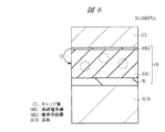
続いて、図2に示すように、基板SUBの主面(p型ウエルPWの表面)上に酸化シリコン(SiO2)から構成される界面層ILを形成した後、界面層IL上に酸化シリコンより高い比誘電率の酸化物から構成される高誘電体層HK1を形成する。この高誘電体層HK1は、nチャネル型MISトランジスタのゲート絶縁膜を構成するものであり、例えば酸化ハフニウム(HfO2)から構成される。界面層ILは、基板SUB(単結晶シリコン)上に直接高誘電体層HK1(酸化ハフニウム)を形成した時に発生する欠陥を低減するために、本実施の形態1では設けられている。また、この界面層ILはゲート絶縁膜に含まれてしまうため、高い比誘電率のゲート絶縁膜を得るためには、その膜厚はできるだけ薄い方が良い。 Subsequently, as shown in FIG. 2, an interface layer IL made of silicon oxide (SiO 2 ) is formed on the main surface (surface of the p-type well PW) of the substrate SUB, and then silicon oxide is formed on the interface layer IL. A high dielectric layer HK1 composed of an oxide having a higher relative dielectric constant is formed. This high dielectric layer HK1 constitutes the gate insulating film of the n-channel MIS transistor, and is made of, for example, hafnium oxide (HfO 2 ). The interface layer IL is provided in the first embodiment in order to reduce defects generated when the high dielectric layer HK1 (hafnium oxide) is directly formed on the substrate SUB (single crystal silicon). In addition, since this interface layer IL is included in the gate insulating film, in order to obtain a gate insulating film having a high relative dielectric constant, the film thickness should be as thin as possible.
本実施の形態1では、界面層ILを構成する酸化シリコン(SiO2)は、例えば、希釈フッ酸溶液で自然酸化膜を除去した後に、基板SUBの主面を950℃以上の高温度熱処理酸化することによって形成され、その膜厚は例えば0.3nmである。 In the first embodiment, silicon oxide (SiO 2 ) constituting the interface layer IL is formed by, for example, removing the natural oxide film with a diluted hydrofluoric acid solution and then subjecting the main surface of the substrate SUB to high-temperature heat treatment oxidation at 950 ° C. or higher. The film thickness is 0.3 nm, for example.
また、高誘電体層HK1を構成する酸化ハフニウム(HfO2)は、例えば、H2O(水)のO(酸素)原料とTDMAH(Tetrakis-Dimethylamido-Hafnium:Hf(NMe2)4)のHf(ハフニウム)原料を用いた原子層制御成膜(ALD:Atomic Layer Deposition)法によって堆積され、その膜厚は例えば2.4nmである。 The hafnium oxide (HfO 2 ) constituting the high dielectric layer HK1 is, for example, an O (oxygen) source of H 2 O (water) and Hf of TDMAH (Tetrakis-Dimethylamido-Hafnium: Hf (NMe 2 ) 4 ). Deposited by an atomic layer deposition (ALD) method using (hafnium) raw material, and the film thickness is, for example, 2.4 nm.
ここで、高誘電体層HK1は、酸化ハフニウム(Hf−O)の他に、例えば、Hf−Si−O、Hf−Si−O−N、Hf−Al−O、Hf−Al−O−N、Hf-Ta-O、Hf−Ti−O、Hf−La−O、Hf−Y−O、Hf−Ta−Si−O、Hf−Ti−Si−O、Hf−La−Si−O、Hf−Y−Si−Oなどの酸化物も適用することができる。このような酸素(O)とハフニウム(Hf)を含み、酸化シリコン(SiO2)より高い比誘電率のものを本願においては「ハフニウム系酸化物」と称している。 Here, the high dielectric layer HK1 includes, for example, Hf—Si—O, Hf—Si—O—N, Hf—Al—O, and Hf—Al—O—N in addition to hafnium oxide (Hf—O). Hf—Ta—O, Hf—Ti—O, Hf—La—O, Hf—Y—O, Hf—Ta—Si—O, Hf—Ti—Si—O, Hf—La—Si—O, Hf An oxide such as -Y-Si-O can also be used. Such a material containing oxygen (O) and hafnium (Hf) and having a relative dielectric constant higher than that of silicon oxide (SiO 2 ) is referred to as “hafnium-based oxide” in the present application.
ハフニウム系酸化物を形成するにあたりALD法を用いた場合、H2OガスのO原料とTDMAH(Hf(NMe2)4)のHf原料の他に、それぞれの原料が用いられる。Si(シリコン)原料としては、例えばTDMAS(Trisdimethlaminosilane:HSi(NMe2)3)である。Al(アルミニウム)原料としては、例えばTMA(Trimethylaluminum:AlMe3)である。Ta(タンタル)原料としては、例えばTAIDEAT(tertiaryamylimidotris(dimethlamido)tantalum:EtMe2CNTa(NMe2)3)である。Ti(チタン)原料としては、例えばTDMAT(Tetrakisdimethylaminotitanium:Ti(NMe2)3)、である。Y(イットリウム)原料としては、例えばTrisethylcyclopentadienylyttrium:Y(EtCp)3である。La(ランタン)原料としては、例えばTrisethylcyclopentadienyllanthanum:La(EtCp)3である。また、Hf−Si−O−N及びHf−Al−O−Nの窒化は、Hf−Si−O、Hf−Al−O膜をALD法で堆積した後に、プラズマ窒素による窒化及びアンモンアガスを用いた熱処理による窒化によって作製される。 When the ALD method is used for forming the hafnium-based oxide, each raw material is used in addition to the O raw material of H 2 O gas and the Hf raw material of TDMAH (Hf (NMe 2 ) 4 ). An example of the Si (silicon) material is TDMAS (Trisdimethlaminosilane: HSi (NMe 2 ) 3 ). An example of the Al (aluminum) raw material is TMA (Trimethylaluminum: AlMe 3 ). An example of the Ta (tantalum) raw material is TAIDEAT (tertiaryamylimidotris (dimethlamido) tantalum: EtMe 2 CNTa (NMe 2 ) 3 ). An example of the Ti (titanium) raw material is TDMAT (Tetrakisdimethylaminotitanium: Ti (NMe 2 ) 3 ). The Y (yttrium) raw material is, for example, Trisethylcyclopentadienylyttrium: Y (EtCp) 3 . The La (lanthanum) raw material is, for example, Trisethylcyclopentadienyllanthanum: La (EtCp) 3 . The nitriding of Hf—Si—O—N and Hf—Al—O—N was performed by depositing Hf—Si—O and Hf—Al—O films by the ALD method, and then using nitriding with plasma nitrogen and Ammon Agas. It is produced by nitriding by heat treatment.
また、本実施の形態1では、高誘電体層HK1の形成にあたりALD法を適用しているが、これに限らず、スパッタリング法、CVD法によって形成されても良い。なお、後の工程でも、ハフニウム系酸化物を堆積して酸素供給層を構成するが、このハフニウム系酸化物は、スパッタリング法、CVD法を適用せず、ALD法を適用している。 In the first embodiment, the ALD method is applied to form the high dielectric layer HK1. However, the present invention is not limited to this, and the high dielectric layer HK1 may be formed by a sputtering method or a CVD method. In the subsequent steps, hafnium-based oxide is deposited to form an oxygen supply layer, but this hafnium-based oxide applies the ALD method without applying the sputtering method or the CVD method.
続いて、図3に示すように、酸素濃度がppm(parts per million)以下の非酸化性雰囲気(例えば窒素、水素、アルゴンなど)中において600℃〜1000℃の範囲で基板SUBの主面を熱処理する。この工程では高誘電体層HK1を緻密化する。なお、本願においては、高誘電体層HK1を緻密化する熱処理を「緻密化アニール」という。 Subsequently, as shown in FIG. 3, the main surface of the substrate SUB is formed in the range of 600 ° C. to 1000 ° C. in a non-oxidizing atmosphere (for example, nitrogen, hydrogen, argon, etc.) having an oxygen concentration of ppm (parts per million) or less. Heat treatment. In this step, the high dielectric layer HK1 is densified. In the present application, the heat treatment for densifying the high dielectric layer HK1 is referred to as “densification annealing”.
堆積されたままの高誘電体層HK1は、原料に起因した炭素等の不純物やH2O酸化剤に起因したOH等の不純物が膜中に残存するために比較的密度が低くなり、その結果、誘電率が低い。そこで、成膜後に緻密化アニールを行うことによって、高誘電体層HK1の緻密化および高誘電率化を図ることができる。 The as-deposited high dielectric layer HK1 has a relatively low density because impurities such as carbon due to the raw materials and impurities such as OH due to the H 2 O oxidant remain in the film. The dielectric constant is low. Therefore, by performing densification annealing after film formation, the high dielectric layer HK1 can be densified and the dielectric constant can be increased.
また、非酸化性雰囲気中で緻密化アニールを行うことによって、基板SUB(単結晶シリコン)界面におけるSi−O結合の形成を防止することができる。酸素(O)を含む雰囲気中で緻密化アニールを行った場合は、外部から酸素が酸化ハフニウムから構成される高誘電体層HK1中を拡散して酸素が単結晶シリコンから構成される基板SUBまで到達して、単結晶シリコンから構成される基板SUBとの界面でSi−O結合を形成する。その結果、ゲート絶縁膜の一部が酸化シリコン膜になる、すなわち酸化シリコンから構成される界面層ILが厚くなり、ゲート絶縁膜の誘電率が低下してしまう。そこで、非酸化性雰囲気中で緻密化アニールを行うことによって、界面におけるSi−O結合の形成を防止することができるのである。 Further, by performing densification annealing in a non-oxidizing atmosphere, formation of Si—O bonds at the substrate SUB (single crystal silicon) interface can be prevented. When densification annealing is performed in an atmosphere containing oxygen (O), oxygen diffuses from the outside into the high dielectric layer HK1 composed of hafnium oxide to the substrate SUB composed of single crystal silicon. The Si—O bond is formed at the interface with the substrate SUB made of single crystal silicon. As a result, a part of the gate insulating film becomes a silicon oxide film, that is, the interface layer IL made of silicon oxide becomes thick, and the dielectric constant of the gate insulating film decreases. Therefore, formation of Si—O bonds at the interface can be prevented by performing densification annealing in a non-oxidizing atmosphere.
さらに、緻密化アニール工程を行うにあたり、非酸化性雰囲気中で、かつ急加熱・急冷(例えば、1000℃/sec)の急速加熱処理(PDA:Post Deposition Annealing)で行う場合、酸化シリコンから構成される界面層ILの膜厚をより厚くすることなく、高誘電体層HK1を緻密化することができる。 Further, when performing the densification annealing step, it is composed of silicon oxide when performing rapid heating treatment (PDA: Post Deposition Annealing) in a non-oxidizing atmosphere and rapid heating / cooling (for example, 1000 ° C./sec). The high dielectric layer HK1 can be densified without increasing the thickness of the interface layer IL.
しかしながら、この緻密化アニールを行うことによって、緻密化を保持したまま酸素(O)が欠損してしまう。図3では、欠損した酸素が雰囲気中に放出されて、高誘電体層HK1中に酸素欠損部DPが発生する様子が示されている。なお、後述の工程(酸素供給アニール工程)で、この酸素欠損部DPを低減する処理が行われる。 However, by performing this densification annealing, oxygen (O) is lost while maintaining the densification. FIG. 3 shows a state in which the deficient oxygen is released into the atmosphere and the oxygen deficient portion DP is generated in the high dielectric layer HK1. In addition, the process which reduces this oxygen deficient part DP is performed by the below-mentioned process (oxygen supply annealing process).
続いて、図4に示すように、緻密化アニール直後の高誘電体層HK1中に占める酸素の割合より高い酸化物から構成される酸素供給層HK2を形成する。本実施の形態1では、緻密化アニール直後の酸素欠損している高誘電体層HK1中に占める酸素の割合より高い酸素供給層HK2として、例えばH2OのO(酸素)原料とTDMAH(Hf(NMe2)4)のHf(ハフニウム)原料を用いたALD法によって堆積されたハフニウム系酸化物膜を適用することができる。ALD法はチャンバー内に設置した基板SUB上に、原料化合物の分子をモノレイヤごとに表面へ吸着、反応による成膜、パージによる余剰分子の取り除き、H2O酸化材との反応による成膜、パージによる余剰分子の取り除き、のサイクルを繰返し行うことによって、原子層を一層ずつ堆積する方法である。このためサイクル数によってハフニウム系酸化物膜から構成される酸素供給層HK2の膜厚を制御することができる。 Subsequently, as shown in FIG. 4, an oxygen supply layer HK2 composed of an oxide higher than the proportion of oxygen in the high dielectric layer HK1 immediately after the densification annealing is formed. In the first embodiment, as the oxygen supply layer HK2 having a higher proportion of oxygen in the oxygen-deficient high dielectric layer HK1 immediately after the densification annealing, for example, an O (oxygen) source material of H 2 O and TDMAH (Hf A hafnium-based oxide film deposited by an ALD method using an Hf (hafnium) source material of (NMe 2 ) 4 ) can be applied. In the ALD method, on the substrate SUB installed in the chamber, the raw material compound molecules are adsorbed to the surface for each monolayer, formed by reaction, removal of excess molecules by purge, formation by reaction with H 2 O oxide, and purge This is a method of depositing atomic layers one layer at a time by repeating the cycle of removing excess molecules. For this reason, the film thickness of the oxygen supply layer HK2 composed of the hafnium-based oxide film can be controlled by the number of cycles.
ALD法によって堆積されたハフニウム系酸化物膜中には、定量的に残留OH基が含まれる。このため緻密化アニール直後の酸素欠損しているハフニウム系酸化物膜(高誘電体層HK1)中に占める酸素の割合よりハフニウム系酸化物膜(酸素供給層HK2)中に占める酸素の割合が高いこととなる。残留した酸素が後述の工程で、高誘電体層HK1で欠損している酸素を補う(供給する)役割をし、すなわち酸素供給層HK2は酸素供給源として働き、その膜厚で絶対供給量を調整することができる。このため原子レベルで膜厚を制御することができるALD法は、酸素供給層HK2の形成には有効となる。 Residual OH groups are quantitatively contained in the hafnium-based oxide film deposited by the ALD method. For this reason, the ratio of oxygen in the hafnium-based oxide film (oxygen supply layer HK2) is higher than the ratio of oxygen in the oxygen-deficient hafnium-based oxide film (high dielectric layer HK1) immediately after the densification annealing. It will be. Residual oxygen serves to supplement (supply) oxygen deficient in the high dielectric layer HK1 in a later-described process. That is, the oxygen supply layer HK2 functions as an oxygen supply source, and the absolute supply amount is determined by the film thickness. Can be adjusted. Therefore, the ALD method capable of controlling the film thickness at the atomic level is effective for forming the oxygen supply layer HK2.
例えば、ALD法によって堆積された酸化ハフニウム膜中には、原料としてH2Oを用いるため、約0.5%の残留OH基が含まれる。図10にALD法によって堆積された酸化ハフニウム膜の厚さに対する残留OH基の含有量を示す。図10に示すように、サイクル数が増加するに従い、すなわち膜厚が厚くなるに従い、酸化ハフニウム膜中に含まれるOH基が増加することがわかる。したがって、緻密化アニールによって酸素欠損が生じた高誘電体層HK1に対して充分に酸素を供給できるように、ALD法によって堆積された酸化ハフニウムから構成される酸素供給層HK2の膜厚で、絶対供給量を調整する。本実施の形態1では、ALD法によって堆積された酸化ハフニウム膜から構成される酸素供給層HK2の膜厚を例えば4Åと調整している。 For example, a hafnium oxide film deposited by the ALD method contains about 0.5% residual OH groups because H 2 O is used as a raw material. FIG. 10 shows the residual OH group content with respect to the thickness of the hafnium oxide film deposited by the ALD method. As shown in FIG. 10, it can be seen that the number of OH groups contained in the hafnium oxide film increases as the number of cycles increases, that is, as the film thickness increases. Accordingly, the thickness of the oxygen supply layer HK2 made of hafnium oxide deposited by the ALD method is sufficiently large so that oxygen can be sufficiently supplied to the high dielectric layer HK1 in which oxygen vacancies are generated by densification annealing. Adjust the supply amount. In the first embodiment, the film thickness of the oxygen supply layer HK2 composed of a hafnium oxide film deposited by the ALD method is adjusted to 4 mm, for example.
ところで、ハフニウム系酸化物を形成する方法にはALD法の他に、スパッタリング法あるいはCVD法などがある。しかしながら、スパッタリング法あるいはCVD法では、堆積された膜中の酸素が過剰とはならず、緻密化アニール直後の酸素欠損している高誘電体層HK1中に占める酸素の割合より高い酸素供給層HK2を形成することができない。このため、H2Oを原料としたALD法を用いている。 Incidentally, as a method for forming a hafnium-based oxide, there are a sputtering method, a CVD method, and the like in addition to the ALD method. However, in the sputtering method or the CVD method, the oxygen in the deposited film does not become excessive, and the oxygen supply layer HK2 is higher than the proportion of oxygen in the high-dielectric layer HK1 that is oxygen deficient immediately after the densification annealing. Can not form. For this reason, the ALD method using H 2 O as a raw material is used.
続いて、図5に示すように、酸素供給層HK2上に、酸素が拡散するのを防止する金属から構成されるキャップ層CLを形成する。言い換えると、酸素供給層HK2をキャップ層CLによってキャップする。キャップ層CLは、後の工程(酸素供給アニール工程)で基板SUBの主面を熱処理した場合において、熱処理時の雰囲気中に酸素が放出しないようにする(バリヤする)ために設けられる金属膜(バリアメタル膜)から構成されるものである。本実施の形態1では、キャップ層CLは、例えばスパッタリング法を用いて形成された窒化タンタル(TaN)から構成され、その膜厚は例えば20nmである。 Subsequently, as shown in FIG. 5, a cap layer CL made of a metal that prevents oxygen from diffusing is formed on the oxygen supply layer HK2. In other words, the oxygen supply layer HK2 is capped by the cap layer CL. The cap layer CL is a metal film provided to prevent oxygen from being released (barriered) into the atmosphere during heat treatment when the main surface of the substrate SUB is heat-treated in a subsequent process (oxygen supply annealing process). Barrier metal film). In the first embodiment, the cap layer CL is made of tantalum nitride (TaN) formed by using, for example, a sputtering method, and the film thickness thereof is, for example, 20 nm.
続いて、図6に示すように、例えば窒素(N2)雰囲気中で950℃〜1150℃の範囲で基板SUBの主面を熱処理する。この工程では、酸素供給層HK2中で残存している酸素を、高誘電体層HK1に供給し、高誘電体層HK1の酸素欠損を補う。すなわち、図3で説明した緻密化アニールを行うことによって生じた酸素欠損部DPを低減する。なお、本願においては、高誘電体層HK1に酸素を供給する熱処理を「酸素供給アニール」という。 Subsequently, as shown in FIG. 6, the main surface of the substrate SUB is heat-treated in a range of 950 ° C. to 1150 ° C., for example, in a nitrogen (N 2 ) atmosphere. In this step, oxygen remaining in the oxygen supply layer HK2 is supplied to the high dielectric layer HK1 to compensate for oxygen vacancies in the high dielectric layer HK1. That is, the oxygen deficient portion DP generated by performing the densification annealing described with reference to FIG. 3 is reduced. In the present application, the heat treatment for supplying oxygen to the high dielectric layer HK1 is referred to as “oxygen supply annealing”.
このようにして酸素が補われた高誘電体層HK1は、界面層IL、酸素供給層HK2も含み、ゲート絶縁膜GIを構成する。本実施の形態1では、酸素供給層HK2として、ハフニウム系酸化物を用いているが、緻密化アニール直後の高誘電体層HK1中に占める酸素の割合より高い酸化物であれば良い。しかしながら、高誘電率のゲート絶縁膜GIを得るためには、ハフニウム系酸化物のように、酸素供給層HK2も酸化シリコンより高い比誘電率の酸化物が望ましい。 The high dielectric layer HK1 supplemented with oxygen in this way also includes the interface layer IL and the oxygen supply layer HK2, and constitutes the gate insulating film GI. In the first embodiment, a hafnium-based oxide is used as the oxygen supply layer HK2, but any oxide higher than the proportion of oxygen in the high dielectric layer HK1 immediately after the densification annealing may be used. However, in order to obtain the gate insulating film GI having a high dielectric constant, the oxygen supply layer HK2 is preferably an oxide having a higher relative dielectric constant than that of silicon oxide, such as a hafnium-based oxide.
緻密化アニールによって高誘電体層HK1は緻密化を図れる反面、酸素が欠損してしまい、酸素が低密度な膜となる。ゲート絶縁膜GIにこのような酸素が低密度な膜を適用した場合、高密度な膜の場合と比較して高いゲート・リーク電流が流れてしまう。そこで、酸素供給アニールを行うことによって、高誘電体層HK1の酸素欠損を補い、高密度な膜を形成することができ、ゲート・リーク電流が流れるのを抑制することができる。また、酸素供給アニールにおいて、酸素供給層HK2の膜厚、すなわち酸素供給量は調整されるため、例えば基板SUB(単結晶シリコン)界面にまで酸素が到達せず、界面層ILの厚さを厚くしないこともできる。 Although the high dielectric layer HK1 can be densified by densification annealing, oxygen is lost and a film with low density of oxygen is formed. When such a low-density oxygen film is applied to the gate insulating film GI, a higher gate leakage current flows than in the case of a high-density film. Therefore, by performing oxygen supply annealing, oxygen vacancies in the high dielectric layer HK1 can be compensated, a high-density film can be formed, and the flow of gate leakage current can be suppressed. In addition, since the film thickness of the oxygen supply layer HK2, that is, the oxygen supply amount is adjusted in the oxygen supply annealing, for example, oxygen does not reach the substrate SUB (single crystal silicon) interface, and the interface layer IL is thickened. You can not.
これまでの緻密化アニールおよび酸素供給アニールを含む工程によって、ゲート絶縁膜GIを構成する高誘電体層HK1の高誘電率化と、酸素欠損の低減化とを両立することができる。 By the steps including the densification annealing and the oxygen supply annealing so far, it is possible to achieve both high dielectric constant of the high dielectric layer HK1 constituting the gate insulating film GI and reduction of oxygen deficiency.
続いて、図7に示すように、キャップ層CLを構成するバリアメタル膜をパターニングすることによって、バリアメタル膜から構成されるゲート電極GEを形成し、また、ゲート電極GE下以外のゲート絶縁膜GIを除去する。なお、本実施の形態1では、酸素供給アニール後に、ゲート電極GE形成のパターニングを行ったが、その順番が逆になっても良い。 Subsequently, as shown in FIG. 7, the barrier metal film constituting the cap layer CL is patterned to form the gate electrode GE composed of the barrier metal film, and the gate insulating film other than under the gate electrode GE Remove GI. In the first embodiment, the patterning for forming the gate electrode GE is performed after the oxygen supply annealing, but the order may be reversed.
本実施の形態1では、キャップ層CLを構成するバリアメタル膜をパターニングしてゲート電極GEを形成する。このため、キャップ層CLには、酸素が拡散するのを抑制させる役割をし、ゲート電極GEの仕事関数に適したバリアメタルであれば良い。nチャネル型MISトランジスタのキャップ層CLとしては窒化タンタルの他に、アルミニウム(Al)、チタン(Ti)、タンタル(Ta)などを適用することができる。また、pチャネル型MISトランジスタのキャップ層CLとしては、ルテニウム(Ru)、白金(Pt)、ニッケル(Ni)などを適用することができる。 In the first embodiment, the gate electrode GE is formed by patterning the barrier metal film constituting the cap layer CL. Therefore, the cap layer CL may be any barrier metal that serves to suppress oxygen diffusion and is suitable for the work function of the gate electrode GE. As the cap layer CL of the n-channel MIS transistor, aluminum (Al), titanium (Ti), tantalum (Ta), or the like can be applied in addition to tantalum nitride. Further, ruthenium (Ru), platinum (Pt), nickel (Ni), or the like can be applied as the cap layer CL of the p-channel MIS transistor.
また、本実施の形態1では、キャップ層CLおよびゲート電極GEとも窒化タンタルから構成したが、キャップ層CLに窒化タンタルを用いて酸素供給アニールをした後、その窒化タンタルを除去した後、最適な仕事関数の金属材料からゲート電極GEを形成しても良い。 In the first embodiment, both the cap layer CL and the gate electrode GE are made of tantalum nitride. However, after the tantalum nitride is removed by performing oxygen supply annealing using tantalum nitride for the cap layer CL, an optimum condition is obtained. The gate electrode GE may be formed from a metal material having a work function.
続いて、図8に示すように、p型ウエルPWにリンまたはヒ素をイオン注入してn−型半導体領域SA1を形成する。n−型半導体領域SA1は、nチャネル型MISトランジスタをLDD(Lightly Doped Drain)構造にするために形成する。 Subsequently, as shown in FIG. 8, phosphorus or arsenic is ion-implanted into the p-type well PW to form the n − -type semiconductor region SA1. The n − type semiconductor region SA1 is formed in order to make the n channel type MIS transistor have an LDD (Lightly Doped Drain) structure.
続いて、図9に示すように、ゲート電極GEの側壁にサイドウォールスペーサSSを形成する。サイドウォールスペーサSSは、基板SUB上にCVD法で酸化シリコン膜を堆積した後、この酸化シリコン膜を異方性エッチングすることによって形成される。次いで、p型ウエルPWにリンまたはヒ素をイオン注入した後、基板SUBの主面を熱処理してこれらの不純物を拡散させることにより、p型ウエルPWにn+型半導体領域(ソース・ドレイン)SA2を形成する。その後、配線工程を経て、最終に水素雰囲気下で400℃の熱処理(FGA:Forming Gas Annealing)を行い、nチャネル型MISトランジスタを備えた半導体装置が完成する。 Subsequently, as shown in FIG. 9, sidewall spacers SS are formed on the sidewalls of the gate electrode GE. The sidewall spacer SS is formed by depositing a silicon oxide film on the substrate SUB by a CVD method and then anisotropically etching the silicon oxide film. Next, after phosphorus or arsenic is ion-implanted into the p-type well PW, the main surface of the substrate SUB is heat-treated to diffuse these impurities, whereby the n + -type semiconductor region (source / drain) SA2 is formed in the p-type well PW. Form. Thereafter, a wiring process is performed, and finally a heat treatment (FGA: Forming Gas Annealing) at 400 ° C. is performed in a hydrogen atmosphere to complete a semiconductor device including an n-channel MIS transistor.
図11は、本実施の形態1におけるnチャネル型MISトランジスタ(図11の説明にあたりQnとする)と、本発明者が検討したnチャネル型MISトランジスタ(Q’nとする)のトランジスタ特性を比較した表である。なお、Q’nは、Qnの製造工程のうち酸素供給層HK2(ALD法によって堆積された膜厚4Åの酸化ハフニウム膜)を形成する工程を省略した以外は、同様の工程で製造されたものである。 FIG. 11 compares the transistor characteristics of the n-channel MIS transistor (referred to as Qn in the description of FIG. 11) in the first embodiment and the n-channel MIS transistor (referred to as Q′n) studied by the present inventors. It is a table. Q′n was manufactured in the same process except that the step of forming the oxygen supply layer HK2 (hafnium oxide film having a thickness of 4 mm deposited by the ALD method) in the manufacturing process of Qn was omitted. It is.
図11に示すように、QnおよびQ’nのゲート絶縁膜GIの酸化シリコン換算膜厚(EOT)は、それぞれ1.1nmおよび1.0nmと同程度である。したがって、QnおよびQ’nのトランジスタ特性を比較することができる。トランジスタ特性として、ゲート・リーク電流(Jg)および電子移動度(μ)の比較した場合、Q’nに対してQnではゲート・リーク電流が3桁程度低く、電子移動度が2倍程度高い。 As shown in FIG. 11, the silicon oxide equivalent film thicknesses (EOT) of the gate insulating films GI of Qn and Q′n are approximately the same as 1.1 nm and 1.0 nm, respectively. Therefore, the transistor characteristics of Qn and Q′n can be compared. When the gate leakage current (Jg) and the electron mobility (μ) are compared as transistor characteristics, the gate leakage current is lower by about 3 digits and the electron mobility is about twice as high at Qn than Q′n.
このように実施の形態1によるMISトランジスタは、緻密化アニールおよび酸素供給アニールを含む工程によって、ゲート絶縁膜GIを構成する高誘電体層HK1の高誘電率化と酸素欠損の低減化とを両立することができる。また、酸素欠損を抑制したゲート絶縁膜GIを有するMISトランジスタを形成することによって、トランジスタ特性を向上することができる。さらに、酸素供給アニール時において、界面層ILの成長を抑制することができるために、EOTが1nm以下のゲート絶縁膜GIを有するMISトランジスタを形成することもできる。 As described above, the MIS transistor according to the first embodiment achieves both high dielectric constant of the high dielectric layer HK1 constituting the gate insulating film GI and reduction of oxygen vacancies by a process including densification annealing and oxygen supply annealing. can do. In addition, transistor characteristics can be improved by forming a MIS transistor having a gate insulating film GI in which oxygen vacancies are suppressed. Furthermore, since the growth of the interface layer IL can be suppressed during the oxygen supply annealing, it is possible to form a MIS transistor having a gate insulating film GI having an EOT of 1 nm or less.
(実施の形態2)
前記実施の形態1では、酸素供給層を形成する工程では、ALD法によって堆積したハフニウム系酸化物を適用して形成する場合について説明したが、本実施の形態2では、ALD法によって堆積した酸化アルミニウム(Al2O3)、または、ALD法によって堆積した酸化タンタル(Ta2O5)を適用して形成する場合について説明する。なお、その他の工程は前記実施の形態1と同様である。
(Embodiment 2)
In the first embodiment, in the step of forming the oxygen supply layer, the case where the hafnium-based oxide deposited by the ALD method is applied is described. However, in the second embodiment, the oxidation deposited by the ALD method is described. A case where aluminum (Al 2 O 3 ) or tantalum oxide (Ta 2 O 5 ) deposited by an ALD method is applied is described. The other steps are the same as those in the first embodiment.
前記実施の形態1で説明したように、酸素供給層HK2は、高誘電体層HK1で欠損している酸素分を補うために、酸素供給アニール時に酸素を高誘電体層HK1へ供給するものである。このため酸素供給層HK2には、酸素供給層HK2中に占める酸素の割合が緻密化アニール直後の酸素欠損している高誘電体層HK1中に占める酸素濃度より高いものを適用すれば良い。そこで、H2Oを原料として用いるALD法によって酸化アルミニウム(Al2O3)または酸化タンタル(Ta2O5)を堆積することによって、酸素供給層HK2を構成する。 As described in the first embodiment, the oxygen supply layer HK2 supplies oxygen to the high dielectric layer HK1 during the oxygen supply annealing in order to compensate for the oxygen content missing in the high dielectric layer HK1. is there. For this reason, the oxygen supply layer HK2 may be applied such that the proportion of oxygen in the oxygen supply layer HK2 is higher than the oxygen concentration in the high dielectric layer HK1 in which oxygen is deficient immediately after the densification annealing. Therefore, the oxygen supply layer HK2 is formed by depositing aluminum oxide (Al 2 O 3 ) or tantalum oxide (Ta 2 O 5 ) by an ALD method using H 2 O as a raw material.
本実施の形態2では、酸化アルミニウム(Al2O3)を、例えば、H2OのO(酸素)原料とAl(アルミニウム)原料のTMA(Trimethylaluminum:AlMe3)を用いたALD法によって堆積する。または、酸化タンタル(Ta2O5)を、例えば、H2OのO(酸素)原料とTa(タンタル)原料のTAIDEAT(Tertiaryamylimidotris(dimethlamido)tantalum:EtMe2CNTa(NMe2)3)を用いたALD法によって堆積する。 In the second embodiment, aluminum oxide (Al 2 O 3 ) is deposited by an ALD method using, for example, an O (oxygen) source of H 2 O and TMA (Trimethylaluminum: AlMe 3 ) of an Al (aluminum) source. . Alternatively, tantalum oxide (Ta 2 O 5 ) is used, for example, an O (oxygen) raw material of H 2 O and a TAIDEAT (Tertiaryamylimidotris (dimethlamido) tantalum: EtMe 2 CNTa (NMe 2 ) 3 ) of a Ta (tantalum) raw material. Deposited by ALD method.
図12は、ALD法によって堆積された酸化アルミニウム(Al2O3)および酸化タンタル(Ta2O5)に含まれるOH基の含有量を示すグラフである。また、前記実施の形態1において酸素供給層HK2として用いた酸化ハフニウム(HfO2)に含まれるOH基の含有量も合わせて示す。 FIG. 12 is a graph showing the content of OH groups contained in aluminum oxide (Al 2 O 3 ) and tantalum oxide (Ta 2 O 5 ) deposited by the ALD method. In addition, the content of OH groups contained in hafnium oxide (HfO 2 ) used as the oxygen supply layer HK2 in the first embodiment is also shown.
図12に示すように、HfO2には約0.5%、Al2O3には約0.3%、Ta2O5には約1%のOH基が含まれることがわかる。これが酸素供給源として働き、緻密化アニール直後の高誘電体層HK1のある酸素欠損量に対して、膜厚で絶対供給量を調整することができる。なお、ある酸素欠損量の高誘電体層HK1に対して酸素を供給する場合、約0.5%のOH基が含まれるHfO2に対して約1%のOH基が含まれるTa2O5は、膜厚がHfO2の半分程度で良い。 As shown in FIG. 12, it can be seen that HfO 2 contains about 0.5% OH groups, Al 2 O 3 contains about 0.3%, and Ta 2 O 5 contains about 1% OH groups. This acts as an oxygen supply source, and the absolute supply amount can be adjusted by the film thickness with respect to an oxygen deficiency amount in the high dielectric layer HK1 immediately after the densification annealing. When oxygen is supplied to the high dielectric layer HK1 having a certain amount of oxygen deficiency, Ta 2 O 5 containing about 1% OH groups with respect to HfO 2 containing about 0.5% OH groups. The film thickness may be about half that of HfO 2 .
緻密化アニールによって高誘電体層HK1は緻密化を図れる反面、酸素が欠損してしまい、酸素が低密度な膜となる。酸素供給アニールを行うことによって、高誘電体層HK1の酸素欠損を補い、高密度な膜を形成することができ、ゲート・リーク電流が流れるのを抑制することができる。すなわち、酸素欠損を抑制したゲート絶縁膜GIを形成することによって、トランジスタ特性を向上することができる。 Although the high dielectric layer HK1 can be densified by densification annealing, oxygen is lost and a film with low density of oxygen is formed. By performing oxygen supply annealing, oxygen vacancies in the high dielectric layer HK1 can be compensated, a high-density film can be formed, and the flow of gate leakage current can be suppressed. That is, the transistor characteristics can be improved by forming the gate insulating film GI in which oxygen vacancies are suppressed.
以上、本発明者によってなされた発明を実施の形態に基づき具体的に説明したが、本発明は前記実施の形態に限定されるものではなく、その要旨を逸脱しない範囲で種々変更可能であることはいうまでもない。 As mentioned above, the invention made by the present inventor has been specifically described based on the embodiment. However, the present invention is not limited to the embodiment, and various modifications can be made without departing from the scope of the invention. Needless to say.
例えば、前記実施の形態では、高誘電体層としてハフニウム系酸化物(Hf−O)を例示したが、酸化アルミニウム(Al2O3)、酸化タンタル(Ta2O5)、酸化チタン(TiO2)、酸化ランタン(La2O3)、酸化ジルコニウム(ZrO2)から構成される高誘電体層とした場合にも適用することができる。酸化アルミニウム、酸化タンタル、酸化チタン、酸化ランタン、および酸化ジルコニウムは、前記実施の形態で示したハフニウム系酸化物と同様に、熱処理によって酸素欠損が発生してしまう。しかしながら、酸素供給層中の酸素が、高誘電体層を構成する酸化アルミニウム、酸化タンタル、酸化チタン、酸化ランタン、および酸化ジルコニウムに供給されることによって、高誘電体層の高誘電率化と、高誘電体層中の酸素欠損の低減化とを両立することができる。 For example, in the above embodiment, hafnium-based oxide (Hf—O) is exemplified as the high dielectric layer, but aluminum oxide (Al 2 O 3 ), tantalum oxide (Ta 2 O 5 ), titanium oxide (TiO 2 ). ), Lanthanum oxide (La 2 O 3 ), and zirconium oxide (ZrO 2 ), a high dielectric layer can also be applied. In the case of aluminum oxide, tantalum oxide, titanium oxide, lanthanum oxide, and zirconium oxide, oxygen vacancies are generated by heat treatment in the same manner as the hafnium-based oxide described in the above embodiment. However, the oxygen in the oxygen supply layer is supplied to aluminum oxide, tantalum oxide, titanium oxide, lanthanum oxide, and zirconium oxide constituting the high dielectric layer, thereby increasing the dielectric constant of the high dielectric layer, It is possible to achieve both reduction of oxygen vacancies in the high dielectric layer.
本発明は、半導体装置の製造業に幅広く利用されるものであり、特に、32nmテクノロジ以降のトランジスタ特性に優れた半導体装置の製造に利用されるものである。 The present invention is widely used in the semiconductor device manufacturing industry, and in particular, is used for manufacturing a semiconductor device having excellent transistor characteristics after 32 nm technology.
CL キャップ層
DP 酸素欠損部
GE ゲート電極
GI ゲート絶縁膜
HK1 高誘電体層
HK2 酸素供給層
ID 素子分離溝
IL 界面層
PW p型ウエル
SA1 n−型半導体領域
SA2 n+型半導体領域(ソース・ドレイン)
SS サイドウォールスペーサ
SUB 基板
CL Cap layer DP Oxygen deficient portion GE Gate electrode GI Gate insulating film HK1 High dielectric layer HK2 Oxygen supply layer ID Element isolation trench IL Interface layer PW p-type well SA1 n − type semiconductor region SA2 n + type semiconductor region (source / drain) )
SS Side wall spacer SUB Substrate
Claims (19)
前記半導体基板上に前記ゲート絶縁膜を形成する工程は、
(a)前記半導体基板の主面上に、酸化シリコンより高い比誘電率の酸化物から構成される第1層を形成する工程と、
(b)前記工程(a)の後、前記半導体基板の主面を非酸化性雰囲気中で熱処理する工程と、
(c)前記第1層上に、前記工程(b)直後の第1層中に占める酸素の割合より高い酸化物から構成される第2層を形成する工程と、
(d)前記第2層上に、酸素が拡散するのを抑制する金属から構成されるキャップ層を形成する工程と、
(e)前記工程(d)の後、前記半導体基板の主面を熱処理する工程と、
を含むことを特徴とする半導体装置の製造方法。 A method for manufacturing a semiconductor device, comprising: forming a gate insulating film of a MIS transistor on a semiconductor substrate; and forming a gate electrode of the MIS transistor on the gate insulating film,
Forming the gate insulating film on the semiconductor substrate;
(A) forming a first layer made of an oxide having a relative dielectric constant higher than that of silicon oxide on the main surface of the semiconductor substrate;
(B) After the step (a), a step of heat-treating the main surface of the semiconductor substrate in a non-oxidizing atmosphere;
(C) forming a second layer made of an oxide higher than the proportion of oxygen in the first layer immediately after the step (b) on the first layer;
(D) forming a cap layer made of a metal that suppresses oxygen diffusion on the second layer;
(E) After the step (d), a step of heat-treating the main surface of the semiconductor substrate;
A method for manufacturing a semiconductor device, comprising:
を含むことを特徴とする請求項1記載の半導体装置の製造方法。 (F) forming the gate electrode composed of the cap layer by patterning the cap layer;
The method of manufacturing a semiconductor device according to claim 1, comprising:
(b)前記第1層上に第2層を形成する工程と、(B) forming a second layer on the first layer;
(c)前記第2層上にキャップ層を形成する工程と、(C) forming a cap layer on the second layer;
(d)前記工程(a)〜(c)後に、前記半導体基板の主面を熱処理する工程、(D) a step of heat-treating the main surface of the semiconductor substrate after the steps (a) to (c);
を有し、Have
前記第1及び第2層はMISトランジスタのゲート絶縁膜を構成しており、The first and second layers constitute a gate insulating film of a MIS transistor,
前記キャップ層は前記MISトランジスタのゲート電極を構成しており、The cap layer constitutes a gate electrode of the MIS transistor,
前記第1層はハフニウムと酸素を含んで構成されており、The first layer includes hafnium and oxygen,
前記第2層はアルミニウムと酸素、または、タンタルと酸素を含んで構成されており、The second layer includes aluminum and oxygen, or tantalum and oxygen,
前記第2層の膜厚は、前記第1層の膜厚よりも薄いことを特徴とする半導体装置の製造方法。The method of manufacturing a semiconductor device, wherein the film thickness of the second layer is thinner than the film thickness of the first layer.
前記酸化シリコン膜の膜厚は、前記第1層の膜厚よりも薄いことを特徴とする請求項8〜14の何れか1項に記載の半導体装置の製造方法。15. The method of manufacturing a semiconductor device according to claim 8, wherein a thickness of the silicon oxide film is smaller than a thickness of the first layer.
前記キャップ層は、窒化タンタル、アルミニウム、チタン、または、タンタルによって構成されていることを特徴とする請求項8〜16の何れか1項に記載の半導体装置の製造方法。The method for manufacturing a semiconductor device according to claim 8, wherein the cap layer is made of tantalum nitride, aluminum, titanium, or tantalum.
前記キャップ層は、ルテニウム、プラチナ、または、ニッケルによって構成されていることを特徴とする請求項8〜16の何れか1項に記載の半導体装置の製造方法。The method for manufacturing a semiconductor device according to claim 8, wherein the cap layer is made of ruthenium, platinum, or nickel.
Priority Applications (3)
| Application Number | Priority Date | Filing Date | Title |
|---|---|---|---|
| JP2007128692A JP5103056B2 (en) | 2007-05-15 | 2007-05-15 | Manufacturing method of semiconductor device |
| US12/116,940 US20090011608A1 (en) | 2007-05-15 | 2008-05-07 | Manufacturing method of semiconductor device |
| US12/752,828 US8168547B2 (en) | 2007-05-15 | 2010-04-01 | Manufacturing method of semiconductor device |
Applications Claiming Priority (1)
| Application Number | Priority Date | Filing Date | Title |
|---|---|---|---|
| JP2007128692A JP5103056B2 (en) | 2007-05-15 | 2007-05-15 | Manufacturing method of semiconductor device |
Publications (3)
| Publication Number | Publication Date |
|---|---|
| JP2008288227A JP2008288227A (en) | 2008-11-27 |
| JP2008288227A5 JP2008288227A5 (en) | 2010-06-17 |
| JP5103056B2 true JP5103056B2 (en) | 2012-12-19 |
Family
ID=40147704
Family Applications (1)
| Application Number | Title | Priority Date | Filing Date |
|---|---|---|---|
| JP2007128692A Active JP5103056B2 (en) | 2007-05-15 | 2007-05-15 | Manufacturing method of semiconductor device |
Country Status (2)
| Country | Link |
|---|---|
| US (2) | US20090011608A1 (en) |
| JP (1) | JP5103056B2 (en) |
Families Citing this family (355)
| Publication number | Priority date | Publication date | Assignee | Title |
|---|---|---|---|---|
| US8986456B2 (en) | 2006-10-10 | 2015-03-24 | Asm America, Inc. | Precursor delivery system |
| US8076237B2 (en) * | 2008-05-09 | 2011-12-13 | Asm America, Inc. | Method and apparatus for 3D interconnect |
| US10378106B2 (en) | 2008-11-14 | 2019-08-13 | Asm Ip Holding B.V. | Method of forming insulation film by modified PEALD |
| US8313994B2 (en) * | 2009-03-26 | 2012-11-20 | Tokyo Electron Limited | Method for forming a high-K gate stack with reduced effective oxide thickness |
| US9394608B2 (en) | 2009-04-06 | 2016-07-19 | Asm America, Inc. | Semiconductor processing reactor and components thereof |
| US8071452B2 (en) * | 2009-04-27 | 2011-12-06 | Asm America, Inc. | Atomic layer deposition of hafnium lanthanum oxides |
| JP2010278319A (en) * | 2009-05-29 | 2010-12-09 | Renesas Electronics Corp | Semiconductor device and method of manufacturing the same |
| US8877655B2 (en) | 2010-05-07 | 2014-11-04 | Asm America, Inc. | Systems and methods for thin-film deposition of metal oxides using excited nitrogen-oxygen species |
| US8883270B2 (en) | 2009-08-14 | 2014-11-11 | Asm America, Inc. | Systems and methods for thin-film deposition of metal oxides using excited nitrogen—oxygen species |
| US8802201B2 (en) | 2009-08-14 | 2014-08-12 | Asm America, Inc. | Systems and methods for thin-film deposition of metal oxides using excited nitrogen-oxygen species |
| JP5569253B2 (en) * | 2010-08-24 | 2014-08-13 | 富士通セミコンダクター株式会社 | Manufacturing method of semiconductor device |
| CN103262250B (en) * | 2010-12-08 | 2014-12-17 | 夏普株式会社 | Semiconductor device and display apparatus |
| US9312155B2 (en) | 2011-06-06 | 2016-04-12 | Asm Japan K.K. | High-throughput semiconductor-processing apparatus equipped with multiple dual-chamber modules |
| US9793148B2 (en) | 2011-06-22 | 2017-10-17 | Asm Japan K.K. | Method for positioning wafers in multiple wafer transport |
| US10364496B2 (en) | 2011-06-27 | 2019-07-30 | Asm Ip Holding B.V. | Dual section module having shared and unshared mass flow controllers |
| US10854498B2 (en) | 2011-07-15 | 2020-12-01 | Asm Ip Holding B.V. | Wafer-supporting device and method for producing same |
| US20130023129A1 (en) | 2011-07-20 | 2013-01-24 | Asm America, Inc. | Pressure transmitter for a semiconductor processing environment |
| US9096931B2 (en) | 2011-10-27 | 2015-08-04 | Asm America, Inc | Deposition valve assembly and method of heating the same |
| US9341296B2 (en) | 2011-10-27 | 2016-05-17 | Asm America, Inc. | Heater jacket for a fluid line |
| US9017481B1 (en) | 2011-10-28 | 2015-04-28 | Asm America, Inc. | Process feed management for semiconductor substrate processing |
| US9005539B2 (en) | 2011-11-23 | 2015-04-14 | Asm Ip Holding B.V. | Chamber sealing member |
| US9167625B2 (en) | 2011-11-23 | 2015-10-20 | Asm Ip Holding B.V. | Radiation shielding for a substrate holder |
| US8633118B2 (en) * | 2012-02-01 | 2014-01-21 | Tokyo Electron Limited | Method of forming thin metal and semi-metal layers by thermal remote oxygen scavenging |
| US9202727B2 (en) | 2012-03-02 | 2015-12-01 | ASM IP Holding | Susceptor heater shim |
| US8865538B2 (en) | 2012-03-30 | 2014-10-21 | Tokyo Electron Limited | Method of integrating buried threshold voltage adjustment layers for CMOS processing |
| US8946830B2 (en) | 2012-04-04 | 2015-02-03 | Asm Ip Holdings B.V. | Metal oxide protective layer for a semiconductor device |
| TWI622664B (en) | 2012-05-02 | 2018-05-01 | Asm智慧財產控股公司 | Phase-stabilized thin films, structures and devices including the thin films, and methods of forming same |
| US8728832B2 (en) | 2012-05-07 | 2014-05-20 | Asm Ip Holdings B.V. | Semiconductor device dielectric interface layer |
| US8921176B2 (en) * | 2012-06-11 | 2014-12-30 | Freescale Semiconductor, Inc. | Modified high-K gate dielectric stack |
| US8933375B2 (en) | 2012-06-27 | 2015-01-13 | Asm Ip Holding B.V. | Susceptor heater and method of heating a substrate |
| US9558931B2 (en) | 2012-07-27 | 2017-01-31 | Asm Ip Holding B.V. | System and method for gas-phase sulfur passivation of a semiconductor surface |
| US9117866B2 (en) | 2012-07-31 | 2015-08-25 | Asm Ip Holding B.V. | Apparatus and method for calculating a wafer position in a processing chamber under process conditions |
| EP2695966B1 (en) | 2012-08-06 | 2018-10-03 | IMEC vzw | ALD method |
| US9659799B2 (en) | 2012-08-28 | 2017-05-23 | Asm Ip Holding B.V. | Systems and methods for dynamic semiconductor process scheduling |
| US9169975B2 (en) | 2012-08-28 | 2015-10-27 | Asm Ip Holding B.V. | Systems and methods for mass flow controller verification |
| KR20140032716A (en) | 2012-09-07 | 2014-03-17 | 삼성전자주식회사 | Semiconductor device and method for fabricating thereof |
| US9021985B2 (en) | 2012-09-12 | 2015-05-05 | Asm Ip Holdings B.V. | Process gas management for an inductively-coupled plasma deposition reactor |
| US9324811B2 (en) | 2012-09-26 | 2016-04-26 | Asm Ip Holding B.V. | Structures and devices including a tensile-stressed silicon arsenic layer and methods of forming same |
| US10714315B2 (en) | 2012-10-12 | 2020-07-14 | Asm Ip Holdings B.V. | Semiconductor reaction chamber showerhead |
| US8865581B2 (en) | 2012-10-19 | 2014-10-21 | Tokyo Electron Limited | Hybrid gate last integration scheme for multi-layer high-k gate stacks |
| US9640416B2 (en) | 2012-12-26 | 2017-05-02 | Asm Ip Holding B.V. | Single-and dual-chamber module-attachable wafer-handling chamber |
| US20160376700A1 (en) | 2013-02-01 | 2016-12-29 | Asm Ip Holding B.V. | System for treatment of deposition reactor |
| US8894870B2 (en) | 2013-02-01 | 2014-11-25 | Asm Ip Holding B.V. | Multi-step method and apparatus for etching compounds containing a metal |
| US9484191B2 (en) | 2013-03-08 | 2016-11-01 | Asm Ip Holding B.V. | Pulsed remote plasma method and system |
| US9589770B2 (en) | 2013-03-08 | 2017-03-07 | Asm Ip Holding B.V. | Method and systems for in-situ formation of intermediate reactive species |
| US8993054B2 (en) | 2013-07-12 | 2015-03-31 | Asm Ip Holding B.V. | Method and system to reduce outgassing in a reaction chamber |
| US9018111B2 (en) | 2013-07-22 | 2015-04-28 | Asm Ip Holding B.V. | Semiconductor reaction chamber with plasma capabilities |
| US9793115B2 (en) | 2013-08-14 | 2017-10-17 | Asm Ip Holding B.V. | Structures and devices including germanium-tin films and methods of forming same |
| US9396934B2 (en) | 2013-08-14 | 2016-07-19 | Asm Ip Holding B.V. | Methods of forming films including germanium tin and structures and devices including the films |
| US9240412B2 (en) | 2013-09-27 | 2016-01-19 | Asm Ip Holding B.V. | Semiconductor structure and device and methods of forming same using selective epitaxial process |
| US9556516B2 (en) | 2013-10-09 | 2017-01-31 | ASM IP Holding B.V | Method for forming Ti-containing film by PEALD using TDMAT or TDEAT |
| US9605343B2 (en) | 2013-11-13 | 2017-03-28 | Asm Ip Holding B.V. | Method for forming conformal carbon films, structures conformal carbon film, and system of forming same |
| US10179947B2 (en) | 2013-11-26 | 2019-01-15 | Asm Ip Holding B.V. | Method for forming conformal nitrided, oxidized, or carbonized dielectric film by atomic layer deposition |
| US10683571B2 (en) | 2014-02-25 | 2020-06-16 | Asm Ip Holding B.V. | Gas supply manifold and method of supplying gases to chamber using same |
| US9447498B2 (en) | 2014-03-18 | 2016-09-20 | Asm Ip Holding B.V. | Method for performing uniform processing in gas system-sharing multiple reaction chambers |
| US10167557B2 (en) | 2014-03-18 | 2019-01-01 | Asm Ip Holding B.V. | Gas distribution system, reactor including the system, and methods of using the same |
| US11015245B2 (en) | 2014-03-19 | 2021-05-25 | Asm Ip Holding B.V. | Gas-phase reactor and system having exhaust plenum and components thereof |
| US9404587B2 (en) | 2014-04-24 | 2016-08-02 | ASM IP Holding B.V | Lockout tagout for semiconductor vacuum valve |
| US10858737B2 (en) | 2014-07-28 | 2020-12-08 | Asm Ip Holding B.V. | Showerhead assembly and components thereof |
| US9543180B2 (en) | 2014-08-01 | 2017-01-10 | Asm Ip Holding B.V. | Apparatus and method for transporting wafers between wafer carrier and process tool under vacuum |
| US9890456B2 (en) | 2014-08-21 | 2018-02-13 | Asm Ip Holding B.V. | Method and system for in situ formation of gas-phase compounds |
| KR102202603B1 (en) * | 2014-09-19 | 2021-01-14 | 삼성전자주식회사 | Semiconductor device and method of fabricating the same |
| US10941490B2 (en) | 2014-10-07 | 2021-03-09 | Asm Ip Holding B.V. | Multiple temperature range susceptor, assembly, reactor and system including the susceptor, and methods of using the same |
| US9657845B2 (en) | 2014-10-07 | 2017-05-23 | Asm Ip Holding B.V. | Variable conductance gas distribution apparatus and method |
| KR102300403B1 (en) | 2014-11-19 | 2021-09-09 | 에이에스엠 아이피 홀딩 비.브이. | Method of depositing thin film |
| KR102263121B1 (en) | 2014-12-22 | 2021-06-09 | 에이에스엠 아이피 홀딩 비.브이. | Semiconductor device and manufacuring method thereof |
| US9478415B2 (en) | 2015-02-13 | 2016-10-25 | Asm Ip Holding B.V. | Method for forming film having low resistance and shallow junction depth |
| US10529542B2 (en) | 2015-03-11 | 2020-01-07 | Asm Ip Holdings B.V. | Cross-flow reactor and method |
| US10276355B2 (en) | 2015-03-12 | 2019-04-30 | Asm Ip Holding B.V. | Multi-zone reactor, system including the reactor, and method of using the same |
| US10458018B2 (en) | 2015-06-26 | 2019-10-29 | Asm Ip Holding B.V. | Structures including metal carbide material, devices including the structures, and methods of forming same |
| US10600673B2 (en) | 2015-07-07 | 2020-03-24 | Asm Ip Holding B.V. | Magnetic susceptor to baseplate seal |
| US10043661B2 (en) | 2015-07-13 | 2018-08-07 | Asm Ip Holding B.V. | Method for protecting layer by forming hydrocarbon-based extremely thin film |
| US9899291B2 (en) | 2015-07-13 | 2018-02-20 | Asm Ip Holding B.V. | Method for protecting layer by forming hydrocarbon-based extremely thin film |
| US10083836B2 (en) | 2015-07-24 | 2018-09-25 | Asm Ip Holding B.V. | Formation of boron-doped titanium metal films with high work function |
| US10087525B2 (en) | 2015-08-04 | 2018-10-02 | Asm Ip Holding B.V. | Variable gap hard stop design |
| US9647114B2 (en) | 2015-08-14 | 2017-05-09 | Asm Ip Holding B.V. | Methods of forming highly p-type doped germanium tin films and structures and devices including the films |
| US9711345B2 (en) | 2015-08-25 | 2017-07-18 | Asm Ip Holding B.V. | Method for forming aluminum nitride-based film by PEALD |
| US9960072B2 (en) | 2015-09-29 | 2018-05-01 | Asm Ip Holding B.V. | Variable adjustment for precise matching of multiple chamber cavity housings |
| US9909214B2 (en) | 2015-10-15 | 2018-03-06 | Asm Ip Holding B.V. | Method for depositing dielectric film in trenches by PEALD |
| US10211308B2 (en) | 2015-10-21 | 2019-02-19 | Asm Ip Holding B.V. | NbMC layers |
| US10322384B2 (en) | 2015-11-09 | 2019-06-18 | Asm Ip Holding B.V. | Counter flow mixer for process chamber |
| US9455138B1 (en) | 2015-11-10 | 2016-09-27 | Asm Ip Holding B.V. | Method for forming dielectric film in trenches by PEALD using H-containing gas |
| US9905420B2 (en) | 2015-12-01 | 2018-02-27 | Asm Ip Holding B.V. | Methods of forming silicon germanium tin films and structures and devices including the films |
| US9607837B1 (en) | 2015-12-21 | 2017-03-28 | Asm Ip Holding B.V. | Method for forming silicon oxide cap layer for solid state diffusion process |
| US9735024B2 (en) | 2015-12-28 | 2017-08-15 | Asm Ip Holding B.V. | Method of atomic layer etching using functional group-containing fluorocarbon |
| US9627221B1 (en) | 2015-12-28 | 2017-04-18 | Asm Ip Holding B.V. | Continuous process incorporating atomic layer etching |
| US11139308B2 (en) | 2015-12-29 | 2021-10-05 | Asm Ip Holding B.V. | Atomic layer deposition of III-V compounds to form V-NAND devices |
| US9754779B1 (en) | 2016-02-19 | 2017-09-05 | Asm Ip Holding B.V. | Method for forming silicon nitride film selectively on sidewalls or flat surfaces of trenches |
| US10468251B2 (en) | 2016-02-19 | 2019-11-05 | Asm Ip Holding B.V. | Method for forming spacers using silicon nitride film for spacer-defined multiple patterning |
| US10529554B2 (en) | 2016-02-19 | 2020-01-07 | Asm Ip Holding B.V. | Method for forming silicon nitride film selectively on sidewalls or flat surfaces of trenches |
| US10501866B2 (en) | 2016-03-09 | 2019-12-10 | Asm Ip Holding B.V. | Gas distribution apparatus for improved film uniformity in an epitaxial system |
| US10343920B2 (en) | 2016-03-18 | 2019-07-09 | Asm Ip Holding B.V. | Aligned carbon nanotubes |
| US9892913B2 (en) | 2016-03-24 | 2018-02-13 | Asm Ip Holding B.V. | Radial and thickness control via biased multi-port injection settings |
| US10087522B2 (en) | 2016-04-21 | 2018-10-02 | Asm Ip Holding B.V. | Deposition of metal borides |
| US10865475B2 (en) | 2016-04-21 | 2020-12-15 | Asm Ip Holding B.V. | Deposition of metal borides and silicides |
| US10190213B2 (en) | 2016-04-21 | 2019-01-29 | Asm Ip Holding B.V. | Deposition of metal borides |
| US10367080B2 (en) | 2016-05-02 | 2019-07-30 | Asm Ip Holding B.V. | Method of forming a germanium oxynitride film |
| US10032628B2 (en) | 2016-05-02 | 2018-07-24 | Asm Ip Holding B.V. | Source/drain performance through conformal solid state doping |
| KR102592471B1 (en) | 2016-05-17 | 2023-10-20 | 에이에스엠 아이피 홀딩 비.브이. | Method of forming metal interconnection and method of fabricating semiconductor device using the same |
| US11453943B2 (en) | 2016-05-25 | 2022-09-27 | Asm Ip Holding B.V. | Method for forming carbon-containing silicon/metal oxide or nitride film by ALD using silicon precursor and hydrocarbon precursor |
| US10388509B2 (en) | 2016-06-28 | 2019-08-20 | Asm Ip Holding B.V. | Formation of epitaxial layers via dislocation filtering |
| US9859151B1 (en) | 2016-07-08 | 2018-01-02 | Asm Ip Holding B.V. | Selective film deposition method to form air gaps |
| US10612137B2 (en) | 2016-07-08 | 2020-04-07 | Asm Ip Holdings B.V. | Organic reactants for atomic layer deposition |
| US9793135B1 (en) | 2016-07-14 | 2017-10-17 | ASM IP Holding B.V | Method of cyclic dry etching using etchant film |
| US10714385B2 (en) | 2016-07-19 | 2020-07-14 | Asm Ip Holding B.V. | Selective deposition of tungsten |
| US10381226B2 (en) | 2016-07-27 | 2019-08-13 | Asm Ip Holding B.V. | Method of processing substrate |
| US9812320B1 (en) | 2016-07-28 | 2017-11-07 | Asm Ip Holding B.V. | Method and apparatus for filling a gap |
| US10177025B2 (en) | 2016-07-28 | 2019-01-08 | Asm Ip Holding B.V. | Method and apparatus for filling a gap |
| US10395919B2 (en) | 2016-07-28 | 2019-08-27 | Asm Ip Holding B.V. | Method and apparatus for filling a gap |
| KR102532607B1 (en) | 2016-07-28 | 2023-05-15 | 에이에스엠 아이피 홀딩 비.브이. | Substrate processing apparatus and method of operating the same |
| US9887082B1 (en) | 2016-07-28 | 2018-02-06 | Asm Ip Holding B.V. | Method and apparatus for filling a gap |
| US10090316B2 (en) | 2016-09-01 | 2018-10-02 | Asm Ip Holding B.V. | 3D stacked multilayer semiconductor memory using doped select transistor channel |
| US10410943B2 (en) | 2016-10-13 | 2019-09-10 | Asm Ip Holding B.V. | Method for passivating a surface of a semiconductor and related systems |
| US10643826B2 (en) | 2016-10-26 | 2020-05-05 | Asm Ip Holdings B.V. | Methods for thermally calibrating reaction chambers |
| US11532757B2 (en) | 2016-10-27 | 2022-12-20 | Asm Ip Holding B.V. | Deposition of charge trapping layers |
| US10435790B2 (en) | 2016-11-01 | 2019-10-08 | Asm Ip Holding B.V. | Method of subatmospheric plasma-enhanced ALD using capacitively coupled electrodes with narrow gap |
| US10229833B2 (en) | 2016-11-01 | 2019-03-12 | Asm Ip Holding B.V. | Methods for forming a transition metal nitride film on a substrate by atomic layer deposition and related semiconductor device structures |
| US10643904B2 (en) | 2016-11-01 | 2020-05-05 | Asm Ip Holdings B.V. | Methods for forming a semiconductor device and related semiconductor device structures |
| US10714350B2 (en) | 2016-11-01 | 2020-07-14 | ASM IP Holdings, B.V. | Methods for forming a transition metal niobium nitride film on a substrate by atomic layer deposition and related semiconductor device structures |
| US10134757B2 (en) | 2016-11-07 | 2018-11-20 | Asm Ip Holding B.V. | Method of processing a substrate and a device manufactured by using the method |
| KR102546317B1 (en) | 2016-11-15 | 2023-06-21 | 에이에스엠 아이피 홀딩 비.브이. | Gas supply unit and substrate processing apparatus including the same |
| US10340135B2 (en) | 2016-11-28 | 2019-07-02 | Asm Ip Holding B.V. | Method of topologically restricted plasma-enhanced cyclic deposition of silicon or metal nitride |
| KR20180068582A (en) | 2016-12-14 | 2018-06-22 | 에이에스엠 아이피 홀딩 비.브이. | Substrate processing apparatus |
| US9916980B1 (en) | 2016-12-15 | 2018-03-13 | Asm Ip Holding B.V. | Method of forming a structure on a substrate |
| US11581186B2 (en) | 2016-12-15 | 2023-02-14 | Asm Ip Holding B.V. | Sequential infiltration synthesis apparatus |
| US11447861B2 (en) | 2016-12-15 | 2022-09-20 | Asm Ip Holding B.V. | Sequential infiltration synthesis apparatus and a method of forming a patterned structure |
| KR20180070971A (en) | 2016-12-19 | 2018-06-27 | 에이에스엠 아이피 홀딩 비.브이. | Substrate processing apparatus |
| US10269558B2 (en) | 2016-12-22 | 2019-04-23 | Asm Ip Holding B.V. | Method of forming a structure on a substrate |
| US10867788B2 (en) | 2016-12-28 | 2020-12-15 | Asm Ip Holding B.V. | Method of forming a structure on a substrate |
| US11390950B2 (en) | 2017-01-10 | 2022-07-19 | Asm Ip Holding B.V. | Reactor system and method to reduce residue buildup during a film deposition process |
| US10655221B2 (en) | 2017-02-09 | 2020-05-19 | Asm Ip Holding B.V. | Method for depositing oxide film by thermal ALD and PEALD |
| US10468261B2 (en) | 2017-02-15 | 2019-11-05 | Asm Ip Holding B.V. | Methods for forming a metallic film on a substrate by cyclical deposition and related semiconductor device structures |
| US10283353B2 (en) | 2017-03-29 | 2019-05-07 | Asm Ip Holding B.V. | Method of reforming insulating film deposited on substrate with recess pattern |
| US10529563B2 (en) | 2017-03-29 | 2020-01-07 | Asm Ip Holdings B.V. | Method for forming doped metal oxide films on a substrate by cyclical deposition and related semiconductor device structures |
| US10103040B1 (en) | 2017-03-31 | 2018-10-16 | Asm Ip Holding B.V. | Apparatus and method for manufacturing a semiconductor device |
| USD830981S1 (en) | 2017-04-07 | 2018-10-16 | Asm Ip Holding B.V. | Susceptor for semiconductor substrate processing apparatus |
| KR102457289B1 (en) | 2017-04-25 | 2022-10-21 | 에이에스엠 아이피 홀딩 비.브이. | Method for depositing a thin film and manufacturing a semiconductor device |
| US10446393B2 (en) | 2017-05-08 | 2019-10-15 | Asm Ip Holding B.V. | Methods for forming silicon-containing epitaxial layers and related semiconductor device structures |
| US10892156B2 (en) | 2017-05-08 | 2021-01-12 | Asm Ip Holding B.V. | Methods for forming a silicon nitride film on a substrate and related semiconductor device structures |
| US10770286B2 (en) | 2017-05-08 | 2020-09-08 | Asm Ip Holdings B.V. | Methods for selectively forming a silicon nitride film on a substrate and related semiconductor device structures |
| US10504742B2 (en) | 2017-05-31 | 2019-12-10 | Asm Ip Holding B.V. | Method of atomic layer etching using hydrogen plasma |
| US10886123B2 (en) | 2017-06-02 | 2021-01-05 | Asm Ip Holding B.V. | Methods for forming low temperature semiconductor layers and related semiconductor device structures |
| US11306395B2 (en) | 2017-06-28 | 2022-04-19 | Asm Ip Holding B.V. | Methods for depositing a transition metal nitride film on a substrate by atomic layer deposition and related deposition apparatus |
| US10685834B2 (en) | 2017-07-05 | 2020-06-16 | Asm Ip Holdings B.V. | Methods for forming a silicon germanium tin layer and related semiconductor device structures |
| KR20190009245A (en) | 2017-07-18 | 2019-01-28 | 에이에스엠 아이피 홀딩 비.브이. | Methods for forming a semiconductor device structure and related semiconductor device structures |
| US10541333B2 (en) | 2017-07-19 | 2020-01-21 | Asm Ip Holding B.V. | Method for depositing a group IV semiconductor and related semiconductor device structures |
| US11374112B2 (en) | 2017-07-19 | 2022-06-28 | Asm Ip Holding B.V. | Method for depositing a group IV semiconductor and related semiconductor device structures |
| US11018002B2 (en) | 2017-07-19 | 2021-05-25 | Asm Ip Holding B.V. | Method for selectively depositing a Group IV semiconductor and related semiconductor device structures |
| US10312055B2 (en) | 2017-07-26 | 2019-06-04 | Asm Ip Holding B.V. | Method of depositing film by PEALD using negative bias |
| US10605530B2 (en) | 2017-07-26 | 2020-03-31 | Asm Ip Holding B.V. | Assembly of a liner and a flange for a vertical furnace as well as the liner and the vertical furnace |
| US10590535B2 (en) | 2017-07-26 | 2020-03-17 | Asm Ip Holdings B.V. | Chemical treatment, deposition and/or infiltration apparatus and method for using the same |
| US10770336B2 (en) | 2017-08-08 | 2020-09-08 | Asm Ip Holding B.V. | Substrate lift mechanism and reactor including same |
| US10692741B2 (en) | 2017-08-08 | 2020-06-23 | Asm Ip Holdings B.V. | Radiation shield |
| US11139191B2 (en) | 2017-08-09 | 2021-10-05 | Asm Ip Holding B.V. | Storage apparatus for storing cassettes for substrates and processing apparatus equipped therewith |
| US10249524B2 (en) | 2017-08-09 | 2019-04-02 | Asm Ip Holding B.V. | Cassette holder assembly for a substrate cassette and holding member for use in such assembly |
| US11769682B2 (en) | 2017-08-09 | 2023-09-26 | Asm Ip Holding B.V. | Storage apparatus for storing cassettes for substrates and processing apparatus equipped therewith |
| US10236177B1 (en) | 2017-08-22 | 2019-03-19 | ASM IP Holding B.V.. | Methods for depositing a doped germanium tin semiconductor and related semiconductor device structures |
| USD900036S1 (en) | 2017-08-24 | 2020-10-27 | Asm Ip Holding B.V. | Heater electrical connector and adapter |
| US11830730B2 (en) | 2017-08-29 | 2023-11-28 | Asm Ip Holding B.V. | Layer forming method and apparatus |
| KR102491945B1 (en) | 2017-08-30 | 2023-01-26 | 에이에스엠 아이피 홀딩 비.브이. | Substrate processing apparatus |
| US11056344B2 (en) | 2017-08-30 | 2021-07-06 | Asm Ip Holding B.V. | Layer forming method |
| US11295980B2 (en) | 2017-08-30 | 2022-04-05 | Asm Ip Holding B.V. | Methods for depositing a molybdenum metal film over a dielectric surface of a substrate by a cyclical deposition process and related semiconductor device structures |
| US10607895B2 (en) | 2017-09-18 | 2020-03-31 | Asm Ip Holdings B.V. | Method for forming a semiconductor device structure comprising a gate fill metal |
| KR102630301B1 (en) | 2017-09-21 | 2024-01-29 | 에이에스엠 아이피 홀딩 비.브이. | Method of sequential infiltration synthesis treatment of infiltrateable material and structures and devices formed using same |
| US10844484B2 (en) | 2017-09-22 | 2020-11-24 | Asm Ip Holding B.V. | Apparatus for dispensing a vapor phase reactant to a reaction chamber and related methods |
| US10658205B2 (en) | 2017-09-28 | 2020-05-19 | Asm Ip Holdings B.V. | Chemical dispensing apparatus and methods for dispensing a chemical to a reaction chamber |
| US10403504B2 (en) | 2017-10-05 | 2019-09-03 | Asm Ip Holding B.V. | Method for selectively depositing a metallic film on a substrate |
| US10319588B2 (en) | 2017-10-10 | 2019-06-11 | Asm Ip Holding B.V. | Method for depositing a metal chalcogenide on a substrate by cyclical deposition |
| US10923344B2 (en) | 2017-10-30 | 2021-02-16 | Asm Ip Holding B.V. | Methods for forming a semiconductor structure and related semiconductor structures |
| KR102443047B1 (en) | 2017-11-16 | 2022-09-14 | 에이에스엠 아이피 홀딩 비.브이. | Method of processing a substrate and a device manufactured by the same |
| US10910262B2 (en) | 2017-11-16 | 2021-02-02 | Asm Ip Holding B.V. | Method of selectively depositing a capping layer structure on a semiconductor device structure |
| US11022879B2 (en) | 2017-11-24 | 2021-06-01 | Asm Ip Holding B.V. | Method of forming an enhanced unexposed photoresist layer |
| CN111344522B (en) | 2017-11-27 | 2022-04-12 | 阿斯莫Ip控股公司 | Including clean mini-environment device |
| KR102597978B1 (en) | 2017-11-27 | 2023-11-06 | 에이에스엠 아이피 홀딩 비.브이. | Storage device for storing wafer cassettes for use with batch furnaces |
| US10290508B1 (en) | 2017-12-05 | 2019-05-14 | Asm Ip Holding B.V. | Method for forming vertical spacers for spacer-defined patterning |
| US10872771B2 (en) | 2018-01-16 | 2020-12-22 | Asm Ip Holding B. V. | Method for depositing a material film on a substrate within a reaction chamber by a cyclical deposition process and related device structures |
| CN111630203A (en) | 2018-01-19 | 2020-09-04 | Asm Ip私人控股有限公司 | Method for depositing gap filling layer by plasma auxiliary deposition |
| TW202325889A (en) | 2018-01-19 | 2023-07-01 | 荷蘭商Asm 智慧財產控股公司 | Deposition method |
| USD903477S1 (en) | 2018-01-24 | 2020-12-01 | Asm Ip Holdings B.V. | Metal clamp |
| US11018047B2 (en) | 2018-01-25 | 2021-05-25 | Asm Ip Holding B.V. | Hybrid lift pin |
| US10535516B2 (en) | 2018-02-01 | 2020-01-14 | Asm Ip Holdings B.V. | Method for depositing a semiconductor structure on a surface of a substrate and related semiconductor structures |
| USD880437S1 (en) | 2018-02-01 | 2020-04-07 | Asm Ip Holding B.V. | Gas supply plate for semiconductor manufacturing apparatus |
| US11081345B2 (en) | 2018-02-06 | 2021-08-03 | Asm Ip Holding B.V. | Method of post-deposition treatment for silicon oxide film |
| US10896820B2 (en) | 2018-02-14 | 2021-01-19 | Asm Ip Holding B.V. | Method for depositing a ruthenium-containing film on a substrate by a cyclical deposition process |
| EP3737779A1 (en) | 2018-02-14 | 2020-11-18 | ASM IP Holding B.V. | A method for depositing a ruthenium-containing film on a substrate by a cyclical deposition process |
| US10731249B2 (en) | 2018-02-15 | 2020-08-04 | Asm Ip Holding B.V. | Method of forming a transition metal containing film on a substrate by a cyclical deposition process, a method for supplying a transition metal halide compound to a reaction chamber, and related vapor deposition apparatus |
| US10658181B2 (en) | 2018-02-20 | 2020-05-19 | Asm Ip Holding B.V. | Method of spacer-defined direct patterning in semiconductor fabrication |
| KR102636427B1 (en) | 2018-02-20 | 2024-02-13 | 에이에스엠 아이피 홀딩 비.브이. | Substrate processing method and apparatus |
| US10975470B2 (en) | 2018-02-23 | 2021-04-13 | Asm Ip Holding B.V. | Apparatus for detecting or monitoring for a chemical precursor in a high temperature environment |
| US11473195B2 (en) | 2018-03-01 | 2022-10-18 | Asm Ip Holding B.V. | Semiconductor processing apparatus and a method for processing a substrate |
| US11629406B2 (en) | 2018-03-09 | 2023-04-18 | Asm Ip Holding B.V. | Semiconductor processing apparatus comprising one or more pyrometers for measuring a temperature of a substrate during transfer of the substrate |
| US11114283B2 (en) | 2018-03-16 | 2021-09-07 | Asm Ip Holding B.V. | Reactor, system including the reactor, and methods of manufacturing and using same |
| KR102646467B1 (en) | 2018-03-27 | 2024-03-11 | 에이에스엠 아이피 홀딩 비.브이. | Method of forming an electrode on a substrate and a semiconductor device structure including an electrode |
| US10510536B2 (en) | 2018-03-29 | 2019-12-17 | Asm Ip Holding B.V. | Method of depositing a co-doped polysilicon film on a surface of a substrate within a reaction chamber |
| US11230766B2 (en) | 2018-03-29 | 2022-01-25 | Asm Ip Holding B.V. | Substrate processing apparatus and method |
| US11088002B2 (en) | 2018-03-29 | 2021-08-10 | Asm Ip Holding B.V. | Substrate rack and a substrate processing system and method |
| KR102501472B1 (en) | 2018-03-30 | 2023-02-20 | 에이에스엠 아이피 홀딩 비.브이. | Substrate processing method |
| TW202344708A (en) | 2018-05-08 | 2023-11-16 | 荷蘭商Asm Ip私人控股有限公司 | Methods for depositing an oxide film on a substrate by a cyclical deposition process and related device structures |
| TWI816783B (en) | 2018-05-11 | 2023-10-01 | 荷蘭商Asm 智慧財產控股公司 | Methods for forming a doped metal carbide film on a substrate and related semiconductor device structures |
| KR102596988B1 (en) | 2018-05-28 | 2023-10-31 | 에이에스엠 아이피 홀딩 비.브이. | Method of processing a substrate and a device manufactured by the same |
| US11270899B2 (en) | 2018-06-04 | 2022-03-08 | Asm Ip Holding B.V. | Wafer handling chamber with moisture reduction |
| US11718913B2 (en) | 2018-06-04 | 2023-08-08 | Asm Ip Holding B.V. | Gas distribution system and reactor system including same |
| US11286562B2 (en) | 2018-06-08 | 2022-03-29 | Asm Ip Holding B.V. | Gas-phase chemical reactor and method of using same |
| KR102568797B1 (en) | 2018-06-21 | 2023-08-21 | 에이에스엠 아이피 홀딩 비.브이. | Substrate processing system |
| US10797133B2 (en) | 2018-06-21 | 2020-10-06 | Asm Ip Holding B.V. | Method for depositing a phosphorus doped silicon arsenide film and related semiconductor device structures |
| US11492703B2 (en) | 2018-06-27 | 2022-11-08 | Asm Ip Holding B.V. | Cyclic deposition methods for forming metal-containing material and films and structures including the metal-containing material |
| WO2020003000A1 (en) | 2018-06-27 | 2020-01-02 | Asm Ip Holding B.V. | Cyclic deposition methods for forming metal-containing material and films and structures including the metal-containing material |
| US10612136B2 (en) | 2018-06-29 | 2020-04-07 | ASM IP Holding, B.V. | Temperature-controlled flange and reactor system including same |
| KR20200002519A (en) | 2018-06-29 | 2020-01-08 | 에이에스엠 아이피 홀딩 비.브이. | Method for depositing a thin film and manufacturing a semiconductor device |
| US10388513B1 (en) | 2018-07-03 | 2019-08-20 | Asm Ip Holding B.V. | Method for depositing silicon-free carbon-containing film as gap-fill layer by pulse plasma-assisted deposition |
| US10755922B2 (en) | 2018-07-03 | 2020-08-25 | Asm Ip Holding B.V. | Method for depositing silicon-free carbon-containing film as gap-fill layer by pulse plasma-assisted deposition |
| US10767789B2 (en) | 2018-07-16 | 2020-09-08 | Asm Ip Holding B.V. | Diaphragm valves, valve components, and methods for forming valve components |
| US10483099B1 (en) | 2018-07-26 | 2019-11-19 | Asm Ip Holding B.V. | Method for forming thermally stable organosilicon polymer film |
| US11053591B2 (en) | 2018-08-06 | 2021-07-06 | Asm Ip Holding B.V. | Multi-port gas injection system and reactor system including same |
| US10883175B2 (en) | 2018-08-09 | 2021-01-05 | Asm Ip Holding B.V. | Vertical furnace for processing substrates and a liner for use therein |
| US10829852B2 (en) | 2018-08-16 | 2020-11-10 | Asm Ip Holding B.V. | Gas distribution device for a wafer processing apparatus |
| US11430674B2 (en) | 2018-08-22 | 2022-08-30 | Asm Ip Holding B.V. | Sensor array, apparatus for dispensing a vapor phase reactant to a reaction chamber and related methods |
| KR20200030162A (en) | 2018-09-11 | 2020-03-20 | 에이에스엠 아이피 홀딩 비.브이. | Method for deposition of a thin film |
| US11024523B2 (en) | 2018-09-11 | 2021-06-01 | Asm Ip Holding B.V. | Substrate processing apparatus and method |
| US11049751B2 (en) | 2018-09-14 | 2021-06-29 | Asm Ip Holding B.V. | Cassette supply system to store and handle cassettes and processing apparatus equipped therewith |
| CN110970344A (en) | 2018-10-01 | 2020-04-07 | Asm Ip控股有限公司 | Substrate holding apparatus, system including the same, and method of using the same |
| US11232963B2 (en) | 2018-10-03 | 2022-01-25 | Asm Ip Holding B.V. | Substrate processing apparatus and method |
| KR102592699B1 (en) | 2018-10-08 | 2023-10-23 | 에이에스엠 아이피 홀딩 비.브이. | Substrate support unit and apparatuses for depositing thin film and processing the substrate including the same |
| US10847365B2 (en) | 2018-10-11 | 2020-11-24 | Asm Ip Holding B.V. | Method of forming conformal silicon carbide film by cyclic CVD |
| US10811256B2 (en) | 2018-10-16 | 2020-10-20 | Asm Ip Holding B.V. | Method for etching a carbon-containing feature |
| KR102605121B1 (en) | 2018-10-19 | 2023-11-23 | 에이에스엠 아이피 홀딩 비.브이. | Substrate processing apparatus and substrate processing method |
| KR102546322B1 (en) | 2018-10-19 | 2023-06-21 | 에이에스엠 아이피 홀딩 비.브이. | Substrate processing apparatus and substrate processing method |
| USD948463S1 (en) | 2018-10-24 | 2022-04-12 | Asm Ip Holding B.V. | Susceptor for semiconductor substrate supporting apparatus |
| US10381219B1 (en) | 2018-10-25 | 2019-08-13 | Asm Ip Holding B.V. | Methods for forming a silicon nitride film |
| US11087997B2 (en) | 2018-10-31 | 2021-08-10 | Asm Ip Holding B.V. | Substrate processing apparatus for processing substrates |
| KR20200051105A (en) | 2018-11-02 | 2020-05-13 | 에이에스엠 아이피 홀딩 비.브이. | Substrate support unit and substrate processing apparatus including the same |
| US11572620B2 (en) | 2018-11-06 | 2023-02-07 | Asm Ip Holding B.V. | Methods for selectively depositing an amorphous silicon film on a substrate |
| US11031242B2 (en) | 2018-11-07 | 2021-06-08 | Asm Ip Holding B.V. | Methods for depositing a boron doped silicon germanium film |
| US10847366B2 (en) | 2018-11-16 | 2020-11-24 | Asm Ip Holding B.V. | Methods for depositing a transition metal chalcogenide film on a substrate by a cyclical deposition process |
| US10818758B2 (en) | 2018-11-16 | 2020-10-27 | Asm Ip Holding B.V. | Methods for forming a metal silicate film on a substrate in a reaction chamber and related semiconductor device structures |
| US10559458B1 (en) | 2018-11-26 | 2020-02-11 | Asm Ip Holding B.V. | Method of forming oxynitride film |
| US11217444B2 (en) | 2018-11-30 | 2022-01-04 | Asm Ip Holding B.V. | Method for forming an ultraviolet radiation responsive metal oxide-containing film |
| KR102636428B1 (en) | 2018-12-04 | 2024-02-13 | 에이에스엠 아이피 홀딩 비.브이. | A method for cleaning a substrate processing apparatus |
| US11158513B2 (en) | 2018-12-13 | 2021-10-26 | Asm Ip Holding B.V. | Methods for forming a rhenium-containing film on a substrate by a cyclical deposition process and related semiconductor device structures |
| JP2020096183A (en) | 2018-12-14 | 2020-06-18 | エーエスエム・アイピー・ホールディング・ベー・フェー | Method of forming device structure using selective deposition of gallium nitride, and system for the same |
| TWI819180B (en) | 2019-01-17 | 2023-10-21 | 荷蘭商Asm 智慧財產控股公司 | Methods of forming a transition metal containing film on a substrate by a cyclical deposition process |
| KR20200091543A (en) | 2019-01-22 | 2020-07-31 | 에이에스엠 아이피 홀딩 비.브이. | Semiconductor processing device |
| CN111524788B (en) | 2019-02-01 | 2023-11-24 | Asm Ip私人控股有限公司 | Method for topologically selective film formation of silicon oxide |
| KR102626263B1 (en) | 2019-02-20 | 2024-01-16 | 에이에스엠 아이피 홀딩 비.브이. | Cyclical deposition method including treatment step and apparatus for same |
| KR20200102357A (en) | 2019-02-20 | 2020-08-31 | 에이에스엠 아이피 홀딩 비.브이. | Apparatus and methods for plug fill deposition in 3-d nand applications |
| TW202044325A (en) | 2019-02-20 | 2020-12-01 | 荷蘭商Asm Ip私人控股有限公司 | Method of filling a recess formed within a surface of a substrate, semiconductor structure formed according to the method, and semiconductor processing apparatus |
| TW202104632A (en) | 2019-02-20 | 2021-02-01 | 荷蘭商Asm Ip私人控股有限公司 | Cyclical deposition method and apparatus for filling a recess formed within a substrate surface |
| TW202100794A (en) | 2019-02-22 | 2021-01-01 | 荷蘭商Asm Ip私人控股有限公司 | Substrate processing apparatus and method for processing substrate |
| KR20200108242A (en) | 2019-03-08 | 2020-09-17 | 에이에스엠 아이피 홀딩 비.브이. | Method for Selective Deposition of Silicon Nitride Layer and Structure Including Selectively-Deposited Silicon Nitride Layer |
| KR20200108243A (en) | 2019-03-08 | 2020-09-17 | 에이에스엠 아이피 홀딩 비.브이. | Structure Including SiOC Layer and Method of Forming Same |
| KR20200108248A (en) | 2019-03-08 | 2020-09-17 | 에이에스엠 아이피 홀딩 비.브이. | STRUCTURE INCLUDING SiOCN LAYER AND METHOD OF FORMING SAME |
| JP2020167398A (en) | 2019-03-28 | 2020-10-08 | エーエスエム・アイピー・ホールディング・ベー・フェー | Door opener and substrate processing apparatus provided therewith |
| KR20200116855A (en) | 2019-04-01 | 2020-10-13 | 에이에스엠 아이피 홀딩 비.브이. | Method of manufacturing semiconductor device |
| KR20200123380A (en) | 2019-04-19 | 2020-10-29 | 에이에스엠 아이피 홀딩 비.브이. | Layer forming method and apparatus |
| KR20200125453A (en) | 2019-04-24 | 2020-11-04 | 에이에스엠 아이피 홀딩 비.브이. | Gas-phase reactor system and method of using same |
| KR20200130118A (en) | 2019-05-07 | 2020-11-18 | 에이에스엠 아이피 홀딩 비.브이. | Method for Reforming Amorphous Carbon Polymer Film |
| KR20200130121A (en) | 2019-05-07 | 2020-11-18 | 에이에스엠 아이피 홀딩 비.브이. | Chemical source vessel with dip tube |
| KR20200130652A (en) | 2019-05-10 | 2020-11-19 | 에이에스엠 아이피 홀딩 비.브이. | Method of depositing material onto a surface and structure formed according to the method |
| JP2020188255A (en) | 2019-05-16 | 2020-11-19 | エーエスエム アイピー ホールディング ビー.ブイ. | Wafer boat handling device, vertical batch furnace, and method |
| USD975665S1 (en) | 2019-05-17 | 2023-01-17 | Asm Ip Holding B.V. | Susceptor shaft |
| USD947913S1 (en) | 2019-05-17 | 2022-04-05 | Asm Ip Holding B.V. | Susceptor shaft |
| USD935572S1 (en) | 2019-05-24 | 2021-11-09 | Asm Ip Holding B.V. | Gas channel plate |
| US11245022B2 (en) | 2019-05-24 | 2022-02-08 | Applied Materials, Inc. | Integrated dipole flow for transistor |
| USD922229S1 (en) | 2019-06-05 | 2021-06-15 | Asm Ip Holding B.V. | Device for controlling a temperature of a gas supply unit |
| KR20200141003A (en) | 2019-06-06 | 2020-12-17 | 에이에스엠 아이피 홀딩 비.브이. | Gas-phase reactor system including a gas detector |
| KR20200143254A (en) | 2019-06-11 | 2020-12-23 | 에이에스엠 아이피 홀딩 비.브이. | Method of forming an electronic structure using an reforming gas, system for performing the method, and structure formed using the method |
| USD944946S1 (en) | 2019-06-14 | 2022-03-01 | Asm Ip Holding B.V. | Shower plate |
| USD931978S1 (en) | 2019-06-27 | 2021-09-28 | Asm Ip Holding B.V. | Showerhead vacuum transport |
| KR20210005515A (en) | 2019-07-03 | 2021-01-14 | 에이에스엠 아이피 홀딩 비.브이. | Temperature control assembly for substrate processing apparatus and method of using same |
| JP2021015791A (en) | 2019-07-09 | 2021-02-12 | エーエスエム アイピー ホールディング ビー.ブイ. | Plasma device and substrate processing method using coaxial waveguide |
| CN112216646A (en) | 2019-07-10 | 2021-01-12 | Asm Ip私人控股有限公司 | Substrate supporting assembly and substrate processing device comprising same |
| KR20210010307A (en) | 2019-07-16 | 2021-01-27 | 에이에스엠 아이피 홀딩 비.브이. | Substrate processing apparatus |
| KR20210010820A (en) | 2019-07-17 | 2021-01-28 | 에이에스엠 아이피 홀딩 비.브이. | Methods of forming silicon germanium structures |
| KR20210010816A (en) | 2019-07-17 | 2021-01-28 | 에이에스엠 아이피 홀딩 비.브이. | Radical assist ignition plasma system and method |
| US11643724B2 (en) | 2019-07-18 | 2023-05-09 | Asm Ip Holding B.V. | Method of forming structures using a neutral beam |
| CN112242296A (en) | 2019-07-19 | 2021-01-19 | Asm Ip私人控股有限公司 | Method of forming topologically controlled amorphous carbon polymer films |
| CN112309843A (en) | 2019-07-29 | 2021-02-02 | Asm Ip私人控股有限公司 | Selective deposition method for achieving high dopant doping |
| CN112309900A (en) | 2019-07-30 | 2021-02-02 | Asm Ip私人控股有限公司 | Substrate processing apparatus |
| CN112309899A (en) | 2019-07-30 | 2021-02-02 | Asm Ip私人控股有限公司 | Substrate processing apparatus |
| US11587815B2 (en) | 2019-07-31 | 2023-02-21 | Asm Ip Holding B.V. | Vertical batch furnace assembly |
| US11227782B2 (en) | 2019-07-31 | 2022-01-18 | Asm Ip Holding B.V. | Vertical batch furnace assembly |
| US11587814B2 (en) | 2019-07-31 | 2023-02-21 | Asm Ip Holding B.V. | Vertical batch furnace assembly |
| KR20210018759A (en) | 2019-08-05 | 2021-02-18 | 에이에스엠 아이피 홀딩 비.브이. | Liquid level sensor for a chemical source vessel |
| USD965044S1 (en) | 2019-08-19 | 2022-09-27 | Asm Ip Holding B.V. | Susceptor shaft |
| USD965524S1 (en) | 2019-08-19 | 2022-10-04 | Asm Ip Holding B.V. | Susceptor support |
| JP2021031769A (en) | 2019-08-21 | 2021-03-01 | エーエスエム アイピー ホールディング ビー.ブイ. | Production apparatus of mixed gas of film deposition raw material and film deposition apparatus |
| USD930782S1 (en) | 2019-08-22 | 2021-09-14 | Asm Ip Holding B.V. | Gas distributor |
| USD949319S1 (en) | 2019-08-22 | 2022-04-19 | Asm Ip Holding B.V. | Exhaust duct |
| KR20210024423A (en) | 2019-08-22 | 2021-03-05 | 에이에스엠 아이피 홀딩 비.브이. | Method for forming a structure with a hole |
| USD940837S1 (en) | 2019-08-22 | 2022-01-11 | Asm Ip Holding B.V. | Electrode |
| USD979506S1 (en) | 2019-08-22 | 2023-02-28 | Asm Ip Holding B.V. | Insulator |
| KR20210024420A (en) | 2019-08-23 | 2021-03-05 | 에이에스엠 아이피 홀딩 비.브이. | Method for depositing silicon oxide film having improved quality by peald using bis(diethylamino)silane |
| US11286558B2 (en) | 2019-08-23 | 2022-03-29 | Asm Ip Holding B.V. | Methods for depositing a molybdenum nitride film on a surface of a substrate by a cyclical deposition process and related semiconductor device structures including a molybdenum nitride film |
| KR20210029090A (en) | 2019-09-04 | 2021-03-15 | 에이에스엠 아이피 홀딩 비.브이. | Methods for selective deposition using a sacrificial capping layer |
| KR20210029663A (en) | 2019-09-05 | 2021-03-16 | 에이에스엠 아이피 홀딩 비.브이. | Substrate processing apparatus |
| US11562901B2 (en) | 2019-09-25 | 2023-01-24 | Asm Ip Holding B.V. | Substrate processing method |
| CN112593212B (en) | 2019-10-02 | 2023-12-22 | Asm Ip私人控股有限公司 | Method for forming topologically selective silicon oxide film by cyclic plasma enhanced deposition process |
| TW202129060A (en) | 2019-10-08 | 2021-08-01 | 荷蘭商Asm Ip控股公司 | Substrate processing device, and substrate processing method |
| KR20210043460A (en) | 2019-10-10 | 2021-04-21 | 에이에스엠 아이피 홀딩 비.브이. | Method of forming a photoresist underlayer and structure including same |
| KR20210045930A (en) | 2019-10-16 | 2021-04-27 | 에이에스엠 아이피 홀딩 비.브이. | Method of Topology-Selective Film Formation of Silicon Oxide |
| US11637014B2 (en) | 2019-10-17 | 2023-04-25 | Asm Ip Holding B.V. | Methods for selective deposition of doped semiconductor material |
| KR20210047808A (en) | 2019-10-21 | 2021-04-30 | 에이에스엠 아이피 홀딩 비.브이. | Apparatus and methods for selectively etching films |
| US11646205B2 (en) | 2019-10-29 | 2023-05-09 | Asm Ip Holding B.V. | Methods of selectively forming n-type doped material on a surface, systems for selectively forming n-type doped material, and structures formed using same |
| KR20210054983A (en) | 2019-11-05 | 2021-05-14 | 에이에스엠 아이피 홀딩 비.브이. | Structures with doped semiconductor layers and methods and systems for forming same |
| US11501968B2 (en) | 2019-11-15 | 2022-11-15 | Asm Ip Holding B.V. | Method for providing a semiconductor device with silicon filled gaps |
| KR20210062561A (en) | 2019-11-20 | 2021-05-31 | 에이에스엠 아이피 홀딩 비.브이. | Method of depositing carbon-containing material on a surface of a substrate, structure formed using the method, and system for forming the structure |
| KR20210065848A (en) | 2019-11-26 | 2021-06-04 | 에이에스엠 아이피 홀딩 비.브이. | Methods for selectivley forming a target film on a substrate comprising a first dielectric surface and a second metallic surface |
| CN112951697A (en) | 2019-11-26 | 2021-06-11 | Asm Ip私人控股有限公司 | Substrate processing apparatus |
| CN112885692A (en) | 2019-11-29 | 2021-06-01 | Asm Ip私人控股有限公司 | Substrate processing apparatus |
| CN112885693A (en) | 2019-11-29 | 2021-06-01 | Asm Ip私人控股有限公司 | Substrate processing apparatus |
| JP2021090042A (en) | 2019-12-02 | 2021-06-10 | エーエスエム アイピー ホールディング ビー.ブイ. | Substrate processing apparatus and substrate processing method |
| KR20210070898A (en) | 2019-12-04 | 2021-06-15 | 에이에스엠 아이피 홀딩 비.브이. | Substrate processing apparatus |
| TW202125596A (en) | 2019-12-17 | 2021-07-01 | 荷蘭商Asm Ip私人控股有限公司 | Method of forming vanadium nitride layer and structure including the vanadium nitride layer |
| KR20210080214A (en) | 2019-12-19 | 2021-06-30 | 에이에스엠 아이피 홀딩 비.브이. | Methods for filling a gap feature on a substrate and related semiconductor structures |
| JP2021109175A (en) | 2020-01-06 | 2021-08-02 | エーエスエム・アイピー・ホールディング・ベー・フェー | Gas supply assembly, components thereof, and reactor system including the same |
| KR20210095050A (en) | 2020-01-20 | 2021-07-30 | 에이에스엠 아이피 홀딩 비.브이. | Method of forming thin film and method of modifying surface of thin film |
| TW202130846A (en) | 2020-02-03 | 2021-08-16 | 荷蘭商Asm Ip私人控股有限公司 | Method of forming structures including a vanadium or indium layer |
| TW202146882A (en) | 2020-02-04 | 2021-12-16 | 荷蘭商Asm Ip私人控股有限公司 | Method of verifying an article, apparatus for verifying an article, and system for verifying a reaction chamber |
| US11776846B2 (en) | 2020-02-07 | 2023-10-03 | Asm Ip Holding B.V. | Methods for depositing gap filling fluids and related systems and devices |
| US11781243B2 (en) | 2020-02-17 | 2023-10-10 | Asm Ip Holding B.V. | Method for depositing low temperature phosphorous-doped silicon |
| US11876356B2 (en) | 2020-03-11 | 2024-01-16 | Asm Ip Holding B.V. | Lockout tagout assembly and system and method of using same |
| KR20210116240A (en) | 2020-03-11 | 2021-09-27 | 에이에스엠 아이피 홀딩 비.브이. | Substrate handling device with adjustable joints |
| KR20210117157A (en) | 2020-03-12 | 2021-09-28 | 에이에스엠 아이피 홀딩 비.브이. | Method for Fabricating Layer Structure Having Target Topological Profile |
| KR20210124042A (en) | 2020-04-02 | 2021-10-14 | 에이에스엠 아이피 홀딩 비.브이. | Thin film forming method |
| TW202146689A (en) | 2020-04-03 | 2021-12-16 | 荷蘭商Asm Ip控股公司 | Method for forming barrier layer and method for manufacturing semiconductor device |
| TW202145344A (en) | 2020-04-08 | 2021-12-01 | 荷蘭商Asm Ip私人控股有限公司 | Apparatus and methods for selectively etching silcon oxide films |
| US11821078B2 (en) | 2020-04-15 | 2023-11-21 | Asm Ip Holding B.V. | Method for forming precoat film and method for forming silicon-containing film |
| KR20210132605A (en) | 2020-04-24 | 2021-11-04 | 에이에스엠 아이피 홀딩 비.브이. | Vertical batch furnace assembly comprising a cooling gas supply |
| US11898243B2 (en) | 2020-04-24 | 2024-02-13 | Asm Ip Holding B.V. | Method of forming vanadium nitride-containing layer |
| KR20210132600A (en) | 2020-04-24 | 2021-11-04 | 에이에스엠 아이피 홀딩 비.브이. | Methods and systems for depositing a layer comprising vanadium, nitrogen, and a further element |
| KR20210134226A (en) | 2020-04-29 | 2021-11-09 | 에이에스엠 아이피 홀딩 비.브이. | Solid source precursor vessel |
| KR20210134869A (en) | 2020-05-01 | 2021-11-11 | 에이에스엠 아이피 홀딩 비.브이. | Fast FOUP swapping with a FOUP handler |
| KR20210141379A (en) | 2020-05-13 | 2021-11-23 | 에이에스엠 아이피 홀딩 비.브이. | Laser alignment fixture for a reactor system |
| KR20210143653A (en) | 2020-05-19 | 2021-11-29 | 에이에스엠 아이피 홀딩 비.브이. | Substrate processing apparatus |
| KR20210145078A (en) | 2020-05-21 | 2021-12-01 | 에이에스엠 아이피 홀딩 비.브이. | Structures including multiple carbon layers and methods of forming and using same |
| TW202201602A (en) | 2020-05-29 | 2022-01-01 | 荷蘭商Asm Ip私人控股有限公司 | Substrate processing device |
| TW202218133A (en) | 2020-06-24 | 2022-05-01 | 荷蘭商Asm Ip私人控股有限公司 | Method for forming a layer provided with silicon |
| TW202217953A (en) | 2020-06-30 | 2022-05-01 | 荷蘭商Asm Ip私人控股有限公司 | Substrate processing method |
| TW202219628A (en) | 2020-07-17 | 2022-05-16 | 荷蘭商Asm Ip私人控股有限公司 | Structures and methods for use in photolithography |
| TW202204662A (en) | 2020-07-20 | 2022-02-01 | 荷蘭商Asm Ip私人控股有限公司 | Method and system for depositing molybdenum layers |
| KR20220027026A (en) | 2020-08-26 | 2022-03-07 | 에이에스엠 아이피 홀딩 비.브이. | Method and system for forming metal silicon oxide and metal silicon oxynitride |
| USD990534S1 (en) | 2020-09-11 | 2023-06-27 | Asm Ip Holding B.V. | Weighted lift pin |
| USD1012873S1 (en) | 2020-09-24 | 2024-01-30 | Asm Ip Holding B.V. | Electrode for semiconductor processing apparatus |
| TW202229613A (en) | 2020-10-14 | 2022-08-01 | 荷蘭商Asm Ip私人控股有限公司 | Method of depositing material on stepped structure |
| KR20220053482A (en) | 2020-10-22 | 2022-04-29 | 에이에스엠 아이피 홀딩 비.브이. | Method of depositing vanadium metal, structure, device and a deposition assembly |
| TW202223136A (en) | 2020-10-28 | 2022-06-16 | 荷蘭商Asm Ip私人控股有限公司 | Method for forming layer on substrate, and semiconductor processing system |
| KR102634254B1 (en) * | 2020-11-18 | 2024-02-05 | 어플라이드 머티어리얼스, 인코포레이티드 | Method of forming semiconductor structure and processing system thereof |
| TW202235675A (en) | 2020-11-30 | 2022-09-16 | 荷蘭商Asm Ip私人控股有限公司 | Injector, and substrate processing apparatus |
| US11946137B2 (en) | 2020-12-16 | 2024-04-02 | Asm Ip Holding B.V. | Runout and wobble measurement fixtures |
| TW202231903A (en) | 2020-12-22 | 2022-08-16 | 荷蘭商Asm Ip私人控股有限公司 | Transition metal deposition method, transition metal layer, and deposition assembly for depositing transition metal on substrate |
| USD980813S1 (en) | 2021-05-11 | 2023-03-14 | Asm Ip Holding B.V. | Gas flow control plate for substrate processing apparatus |
| USD1023959S1 (en) | 2021-05-11 | 2024-04-23 | Asm Ip Holding B.V. | Electrode for substrate processing apparatus |
| USD981973S1 (en) | 2021-05-11 | 2023-03-28 | Asm Ip Holding B.V. | Reactor wall for substrate processing apparatus |
| USD980814S1 (en) | 2021-05-11 | 2023-03-14 | Asm Ip Holding B.V. | Gas distributor for substrate processing apparatus |
| USD990441S1 (en) | 2021-09-07 | 2023-06-27 | Asm Ip Holding B.V. | Gas flow control plate |
Family Cites Families (22)
| Publication number | Priority date | Publication date | Assignee | Title |
|---|---|---|---|---|
| JPH0466376A (en) * | 1990-07-05 | 1992-03-02 | Nissan Motor Co Ltd | Automobile hood structure |
| JPH0574037A (en) * | 1991-09-10 | 1993-03-26 | Sony Corp | Disk reproducing device |
| JP2001185548A (en) * | 1999-12-22 | 2001-07-06 | Fujitsu Ltd | Semiconductor device and manufacturing method thereof |
| JP2001284345A (en) * | 2000-03-29 | 2001-10-12 | Fujitsu Ltd | Method of forming tantalum pentoxide film |
| JP2002043565A (en) * | 2000-07-26 | 2002-02-08 | Toshiba Corp | Manufacturing method of semiconductor device |
| JP3732098B2 (en) * | 2001-02-19 | 2006-01-05 | 株式会社ルネサステクノロジ | Semiconductor device |
| JP3647785B2 (en) * | 2001-09-28 | 2005-05-18 | 株式会社東芝 | Manufacturing method of semiconductor device |
| US6717226B2 (en) * | 2002-03-15 | 2004-04-06 | Motorola, Inc. | Transistor with layered high-K gate dielectric and method therefor |
| JP2003273350A (en) * | 2002-03-15 | 2003-09-26 | Nec Corp | Semiconductor device and method for manufacturing the same |
| JP3647850B2 (en) * | 2002-07-02 | 2005-05-18 | 松下電器産業株式会社 | Semiconductor device and manufacturing method thereof |
| JP4261276B2 (en) * | 2003-08-15 | 2009-04-30 | パナソニック株式会社 | Manufacturing method of semiconductor device |
| US20070023842A1 (en) * | 2003-11-12 | 2007-02-01 | Hyung-Suk Jung | Semiconductor devices having different gate dielectric layers and methods of manufacturing the same |
| KR100568448B1 (en) * | 2004-04-19 | 2006-04-07 | 삼성전자주식회사 | method of fabricating high-k dielectric layer having reduced impurity |
| US8323754B2 (en) * | 2004-05-21 | 2012-12-04 | Applied Materials, Inc. | Stabilization of high-k dielectric materials |
| JP2006086511A (en) * | 2004-08-17 | 2006-03-30 | Nec Electronics Corp | Semiconductor device |
| US7074680B2 (en) * | 2004-09-07 | 2006-07-11 | Intel Corporation | Method for making a semiconductor device having a high-k gate dielectric |
| JP4163164B2 (en) | 2004-09-07 | 2008-10-08 | 株式会社ルネサステクノロジ | Semiconductor device and manufacturing method thereof |
| KR100889362B1 (en) * | 2004-10-19 | 2009-03-18 | 삼성전자주식회사 | Transistor having multi-dielectric layer and fabrication method thereof |
| US20060211259A1 (en) * | 2005-03-21 | 2006-09-21 | Maes Jan W | Silicon oxide cap over high dielectric constant films |
| JP4128574B2 (en) * | 2005-03-28 | 2008-07-30 | 富士通株式会社 | Manufacturing method of semiconductor device |
| US7544596B2 (en) * | 2005-08-30 | 2009-06-09 | Micron Technology, Inc. | Atomic layer deposition of GdScO3 films as gate dielectrics |
| KR100877100B1 (en) * | 2007-04-16 | 2009-01-09 | 주식회사 하이닉스반도체 | Methods for manufacturing non-volatile memory device |
-
2007
- 2007-05-15 JP JP2007128692A patent/JP5103056B2/en active Active
-
2008
- 2008-05-07 US US12/116,940 patent/US20090011608A1/en not_active Abandoned
-
2010
- 2010-04-01 US US12/752,828 patent/US8168547B2/en active Active
Also Published As
| Publication number | Publication date |
|---|---|
| US8168547B2 (en) | 2012-05-01 |
| US20090011608A1 (en) | 2009-01-08 |
| JP2008288227A (en) | 2008-11-27 |
| US20100187644A1 (en) | 2010-07-29 |
Similar Documents
| Publication | Publication Date | Title |
|---|---|---|
| JP5103056B2 (en) | Manufacturing method of semiconductor device | |
| KR100640638B1 (en) | Method for forming high dielectric film by atomic layer deposition and method of fabricating semiconductor device having high dielectric film | |
| US7405482B2 (en) | High-k dielectric film, method of forming the same and related semiconductor device | |
| JP4277268B2 (en) | Method for manufacturing metal compound thin film, and method for manufacturing semiconductor device including the metal compound thin film | |
| US20060199384A1 (en) | Method of forming thin film, and method of manufacturing semiconductor device | |
| JP2006165589A (en) | Method of manufacturing semiconductor device | |
| US7601578B2 (en) | Defect control in gate dielectrics | |
| JP2008532282A (en) | Method of forming a nitrided gate dielectric | |
| US6984565B2 (en) | Method of manufacturing a semiconductor device | |
| JP5127694B2 (en) | Semiconductor device and manufacturing method thereof | |
| JP2006344837A (en) | Semiconductor apparatus and manufacturing method thereof | |
| KR100729354B1 (en) | Methods of manufacturing semiconductor device in order to improve the electrical characteristics of a dielectric | |
| JP2008288226A (en) | Semiconductor device and manufacturing method thereof | |
| JP2010034440A (en) | Semiconductor device and method of manufacturing the same | |
| WO2004107451A1 (en) | Semiconductor device fitted with mis type field-effect transistor, process for producing the same and method of forming metal oxide film | |
| US7592234B2 (en) | Method for forming a nitrogen-containing gate insulating film | |
| JP4477981B2 (en) | Manufacturing method of semiconductor device | |
| US11791153B2 (en) | Deposition of hafnium oxide within a high aspect ratio hole | |
| KR102532520B1 (en) | Semiconductor device with tuned threshold voltage and manufacturing method thereof | |
| JP4220991B2 (en) | Manufacturing method of semiconductor device | |
| KR100755072B1 (en) | Semiconductor device having ternary system oxide gate insulating layer and method of fabricating the same | |
| JP2004289082A (en) | Method of forming high-dielectric-constant gate insulating film | |
| KR100702133B1 (en) | Semiconductor device having TiLaO gate insulating layer and method of fabricating the same | |
| KR100721202B1 (en) | Semiconductor device having ternary system oxide gate insulating layer and method of fabricating the same | |
| KR100650758B1 (en) | Method for forming gate of semiconductor device |
Legal Events
| Date | Code | Title | Description |
|---|---|---|---|
| A521 | Request for written amendment filed |
Free format text: JAPANESE INTERMEDIATE CODE: A523 Effective date: 20100426 |
|
| A621 | Written request for application examination |
Free format text: JAPANESE INTERMEDIATE CODE: A621 Effective date: 20100426 |
|
| A711 | Notification of change in applicant |
Free format text: JAPANESE INTERMEDIATE CODE: A712 Effective date: 20100528 |
|
| TRDD | Decision of grant or rejection written | ||
| A977 | Report on retrieval |
Free format text: JAPANESE INTERMEDIATE CODE: A971007 Effective date: 20120831 |
|
| A01 | Written decision to grant a patent or to grant a registration (utility model) |
Free format text: JAPANESE INTERMEDIATE CODE: A01 Effective date: 20120904 |
|
| A01 | Written decision to grant a patent or to grant a registration (utility model) |
Free format text: JAPANESE INTERMEDIATE CODE: A01 |
|
| A61 | First payment of annual fees (during grant procedure) |
Free format text: JAPANESE INTERMEDIATE CODE: A61 Effective date: 20121001 |
|
| FPAY | Renewal fee payment (event date is renewal date of database) |
Free format text: PAYMENT UNTIL: 20151005 Year of fee payment: 3 |
|
| R150 | Certificate of patent or registration of utility model |
Ref document number: 5103056 Country of ref document: JP Free format text: JAPANESE INTERMEDIATE CODE: R150 Free format text: JAPANESE INTERMEDIATE CODE: R150 |
|
| S531 | Written request for registration of change of domicile |
Free format text: JAPANESE INTERMEDIATE CODE: R313531 |
|
| R350 | Written notification of registration of transfer |
Free format text: JAPANESE INTERMEDIATE CODE: R350 |