JP5085369B2 - Nitride semiconductor light emitting device and manufacturing method thereof - Google Patents
Nitride semiconductor light emitting device and manufacturing method thereof Download PDFInfo
- Publication number
- JP5085369B2 JP5085369B2 JP2008035868A JP2008035868A JP5085369B2 JP 5085369 B2 JP5085369 B2 JP 5085369B2 JP 2008035868 A JP2008035868 A JP 2008035868A JP 2008035868 A JP2008035868 A JP 2008035868A JP 5085369 B2 JP5085369 B2 JP 5085369B2
- Authority
- JP
- Japan
- Prior art keywords
- layer
- nitride semiconductor
- light emitting
- electrode
- type
- Prior art date
- Legal status (The legal status is an assumption and is not a legal conclusion. Google has not performed a legal analysis and makes no representation as to the accuracy of the status listed.)
- Expired - Fee Related
Links
- 239000004065 semiconductor Substances 0.000 title claims description 86
- 150000004767 nitrides Chemical class 0.000 title claims description 79
- 238000004519 manufacturing process Methods 0.000 title claims description 12
- 238000010438 heat treatment Methods 0.000 claims description 36
- 238000000034 method Methods 0.000 claims description 34
- PMHQVHHXPFUNSP-UHFFFAOYSA-M copper(1+);methylsulfanylmethane;bromide Chemical compound Br[Cu].CSC PMHQVHHXPFUNSP-UHFFFAOYSA-M 0.000 claims description 29
- 229910052751 metal Inorganic materials 0.000 claims description 28
- 239000002184 metal Substances 0.000 claims description 28
- 229910052750 molybdenum Inorganic materials 0.000 claims description 8
- 229910052697 platinum Inorganic materials 0.000 claims description 8
- 229910052719 titanium Inorganic materials 0.000 claims description 8
- 238000004544 sputter deposition Methods 0.000 claims description 7
- 229910052735 hafnium Inorganic materials 0.000 claims description 5
- 150000002739 metals Chemical class 0.000 claims description 5
- 229910052726 zirconium Inorganic materials 0.000 claims description 5
- 239000012535 impurity Substances 0.000 claims description 3
- 238000010030 laminating Methods 0.000 claims description 3
- 239000010931 gold Substances 0.000 description 52
- BASFCYQUMIYNBI-UHFFFAOYSA-N platinum Substances [Pt] BASFCYQUMIYNBI-UHFFFAOYSA-N 0.000 description 32
- 239000010936 titanium Substances 0.000 description 24
- 239000000758 substrate Substances 0.000 description 22
- 229910002601 GaN Inorganic materials 0.000 description 18
- 230000000694 effects Effects 0.000 description 14
- 238000005253 cladding Methods 0.000 description 11
- JMASRVWKEDWRBT-UHFFFAOYSA-N Gallium nitride Chemical compound [Ga]#N JMASRVWKEDWRBT-UHFFFAOYSA-N 0.000 description 10
- 229910000679 solder Inorganic materials 0.000 description 8
- 238000009792 diffusion process Methods 0.000 description 7
- 229910052737 gold Inorganic materials 0.000 description 7
- 239000000463 material Substances 0.000 description 7
- KDLHZDBZIXYQEI-UHFFFAOYSA-N palladium Substances [Pd] KDLHZDBZIXYQEI-UHFFFAOYSA-N 0.000 description 7
- 229920002120 photoresistant polymer Polymers 0.000 description 7
- 229910052594 sapphire Inorganic materials 0.000 description 7
- 239000010980 sapphire Substances 0.000 description 7
- 229910002704 AlGaN Inorganic materials 0.000 description 6
- 229910015363 Au—Sn Inorganic materials 0.000 description 5
- 238000002474 experimental method Methods 0.000 description 5
- PCHJSUWPFVWCPO-UHFFFAOYSA-N gold Chemical compound [Au] PCHJSUWPFVWCPO-UHFFFAOYSA-N 0.000 description 5
- 230000004888 barrier function Effects 0.000 description 4
- 238000002845 discoloration Methods 0.000 description 4
- 238000005530 etching Methods 0.000 description 4
- PXHVJJICTQNCMI-UHFFFAOYSA-N nickel Substances [Ni] PXHVJJICTQNCMI-UHFFFAOYSA-N 0.000 description 4
- 229910004298 SiO 2 Inorganic materials 0.000 description 3
- 229910052782 aluminium Inorganic materials 0.000 description 3
- 239000011248 coating agent Substances 0.000 description 3
- 238000000576 coating method Methods 0.000 description 3
- 238000000151 deposition Methods 0.000 description 3
- 238000001312 dry etching Methods 0.000 description 3
- 238000005566 electron beam evaporation Methods 0.000 description 3
- 238000011156 evaluation Methods 0.000 description 3
- 239000007789 gas Substances 0.000 description 3
- 239000012299 nitrogen atmosphere Substances 0.000 description 3
- 238000000206 photolithography Methods 0.000 description 3
- 238000012545 processing Methods 0.000 description 3
- 229910000838 Al alloy Inorganic materials 0.000 description 2
- IJGRMHOSHXDMSA-UHFFFAOYSA-N Atomic nitrogen Chemical compound N#N IJGRMHOSHXDMSA-UHFFFAOYSA-N 0.000 description 2
- ZAMOUSCENKQFHK-UHFFFAOYSA-N Chlorine atom Chemical compound [Cl] ZAMOUSCENKQFHK-UHFFFAOYSA-N 0.000 description 2
- KRHYYFGTRYWZRS-UHFFFAOYSA-N Fluorane Chemical compound F KRHYYFGTRYWZRS-UHFFFAOYSA-N 0.000 description 2
- ZOKXTWBITQBERF-UHFFFAOYSA-N Molybdenum Chemical compound [Mo] ZOKXTWBITQBERF-UHFFFAOYSA-N 0.000 description 2
- RTAQQCXQSZGOHL-UHFFFAOYSA-N Titanium Chemical compound [Ti] RTAQQCXQSZGOHL-UHFFFAOYSA-N 0.000 description 2
- 238000004458 analytical method Methods 0.000 description 2
- 238000000137 annealing Methods 0.000 description 2
- 239000000460 chlorine Substances 0.000 description 2
- 229910052801 chlorine Inorganic materials 0.000 description 2
- 230000008021 deposition Effects 0.000 description 2
- 238000011161 development Methods 0.000 description 2
- 238000010586 diagram Methods 0.000 description 2
- 238000007429 general method Methods 0.000 description 2
- 239000000203 mixture Substances 0.000 description 2
- 239000011733 molybdenum Substances 0.000 description 2
- 229910052758 niobium Inorganic materials 0.000 description 2
- 229910052763 palladium Inorganic materials 0.000 description 2
- 238000005498 polishing Methods 0.000 description 2
- 230000000717 retained effect Effects 0.000 description 2
- 238000012360 testing method Methods 0.000 description 2
- 229910052721 tungsten Inorganic materials 0.000 description 2
- YCKRFDGAMUMZLT-UHFFFAOYSA-N Fluorine atom Chemical compound [F] YCKRFDGAMUMZLT-UHFFFAOYSA-N 0.000 description 1
- QCWXUUIWCKQGHC-UHFFFAOYSA-N Zirconium Chemical compound [Zr] QCWXUUIWCKQGHC-UHFFFAOYSA-N 0.000 description 1
- 239000006061 abrasive grain Substances 0.000 description 1
- 230000002411 adverse Effects 0.000 description 1
- 229910045601 alloy Inorganic materials 0.000 description 1
- 239000000956 alloy Substances 0.000 description 1
- XAGFODPZIPBFFR-UHFFFAOYSA-N aluminium Chemical compound [Al] XAGFODPZIPBFFR-UHFFFAOYSA-N 0.000 description 1
- QVGXLLKOCUKJST-UHFFFAOYSA-N atomic oxygen Chemical compound [O] QVGXLLKOCUKJST-UHFFFAOYSA-N 0.000 description 1
- 230000005540 biological transmission Effects 0.000 description 1
- 230000015572 biosynthetic process Effects 0.000 description 1
- 230000000903 blocking effect Effects 0.000 description 1
- 238000005229 chemical vapour deposition Methods 0.000 description 1
- 238000003776 cleavage reaction Methods 0.000 description 1
- 238000011109 contamination Methods 0.000 description 1
- 238000005336 cracking Methods 0.000 description 1
- 238000002109 crystal growth method Methods 0.000 description 1
- 230000007547 defect Effects 0.000 description 1
- 229910003460 diamond Inorganic materials 0.000 description 1
- 239000010432 diamond Substances 0.000 description 1
- 238000005516 engineering process Methods 0.000 description 1
- 229910052731 fluorine Inorganic materials 0.000 description 1
- 239000011737 fluorine Substances 0.000 description 1
- VBJZVLUMGGDVMO-UHFFFAOYSA-N hafnium atom Chemical compound [Hf] VBJZVLUMGGDVMO-UHFFFAOYSA-N 0.000 description 1
- 125000005842 heteroatom Chemical group 0.000 description 1
- 229910052738 indium Inorganic materials 0.000 description 1
- APFVFJFRJDLVQX-UHFFFAOYSA-N indium atom Chemical compound [In] APFVFJFRJDLVQX-UHFFFAOYSA-N 0.000 description 1
- 238000002347 injection Methods 0.000 description 1
- 239000007924 injection Substances 0.000 description 1
- 238000005259 measurement Methods 0.000 description 1
- 230000008018 melting Effects 0.000 description 1
- 238000002844 melting Methods 0.000 description 1
- 150000002736 metal compounds Chemical class 0.000 description 1
- 239000007769 metal material Substances 0.000 description 1
- 229910044991 metal oxide Inorganic materials 0.000 description 1
- 150000004706 metal oxides Chemical class 0.000 description 1
- 238000002488 metal-organic chemical vapour deposition Methods 0.000 description 1
- 229910052759 nickel Inorganic materials 0.000 description 1
- 239000010955 niobium Substances 0.000 description 1
- 238000005121 nitriding Methods 0.000 description 1
- 229910052757 nitrogen Inorganic materials 0.000 description 1
- 125000002524 organometallic group Chemical group 0.000 description 1
- 239000001301 oxygen Substances 0.000 description 1
- 229910052760 oxygen Inorganic materials 0.000 description 1
- 238000000059 patterning Methods 0.000 description 1
- 230000000630 rising effect Effects 0.000 description 1
- 238000000682 scanning probe acoustic microscopy Methods 0.000 description 1
- 230000007017 scission Effects 0.000 description 1
- 238000005204 segregation Methods 0.000 description 1
- 239000000243 solution Substances 0.000 description 1
- 238000005092 sublimation method Methods 0.000 description 1
- 239000000126 substance Substances 0.000 description 1
- 230000003746 surface roughness Effects 0.000 description 1
- 238000009864 tensile test Methods 0.000 description 1
- 238000002834 transmittance Methods 0.000 description 1
- 238000000927 vapour-phase epitaxy Methods 0.000 description 1
- 238000001947 vapour-phase growth Methods 0.000 description 1
- 238000001039 wet etching Methods 0.000 description 1
Images


Classifications
-
- H—ELECTRICITY
- H01—ELECTRIC ELEMENTS
- H01L—SEMICONDUCTOR DEVICES NOT COVERED BY CLASS H10
- H01L33/00—Semiconductor devices having potential barriers specially adapted for light emission; Processes or apparatus specially adapted for the manufacture or treatment thereof or of parts thereof; Details thereof
- H01L33/36—Semiconductor devices having potential barriers specially adapted for light emission; Processes or apparatus specially adapted for the manufacture or treatment thereof or of parts thereof; Details thereof characterised by the electrodes
- H01L33/40—Materials therefor
-
- B—PERFORMING OPERATIONS; TRANSPORTING
- B82—NANOTECHNOLOGY
- B82Y—SPECIFIC USES OR APPLICATIONS OF NANOSTRUCTURES; MEASUREMENT OR ANALYSIS OF NANOSTRUCTURES; MANUFACTURE OR TREATMENT OF NANOSTRUCTURES
- B82Y20/00—Nanooptics, e.g. quantum optics or photonic crystals
-
- H—ELECTRICITY
- H01—ELECTRIC ELEMENTS
- H01L—SEMICONDUCTOR DEVICES NOT COVERED BY CLASS H10
- H01L33/00—Semiconductor devices having potential barriers specially adapted for light emission; Processes or apparatus specially adapted for the manufacture or treatment thereof or of parts thereof; Details thereof
- H01L33/02—Semiconductor devices having potential barriers specially adapted for light emission; Processes or apparatus specially adapted for the manufacture or treatment thereof or of parts thereof; Details thereof characterised by the semiconductor bodies
- H01L33/26—Materials of the light emitting region
- H01L33/30—Materials of the light emitting region containing only elements of Group III and Group V of the Periodic Table
- H01L33/32—Materials of the light emitting region containing only elements of Group III and Group V of the Periodic Table containing nitrogen
-
- H—ELECTRICITY
- H01—ELECTRIC ELEMENTS
- H01S—DEVICES USING THE PROCESS OF LIGHT AMPLIFICATION BY STIMULATED EMISSION OF RADIATION [LASER] TO AMPLIFY OR GENERATE LIGHT; DEVICES USING STIMULATED EMISSION OF ELECTROMAGNETIC RADIATION IN WAVE RANGES OTHER THAN OPTICAL
- H01S5/00—Semiconductor lasers
- H01S5/30—Structure or shape of the active region; Materials used for the active region
- H01S5/34—Structure or shape of the active region; Materials used for the active region comprising quantum well or superlattice structures, e.g. single quantum well [SQW] lasers, multiple quantum well [MQW] lasers or graded index separate confinement heterostructure [GRINSCH] lasers
- H01S5/343—Structure or shape of the active region; Materials used for the active region comprising quantum well or superlattice structures, e.g. single quantum well [SQW] lasers, multiple quantum well [MQW] lasers or graded index separate confinement heterostructure [GRINSCH] lasers in AIIIBV compounds, e.g. AlGaAs-laser, InP-based laser
- H01S5/34333—Structure or shape of the active region; Materials used for the active region comprising quantum well or superlattice structures, e.g. single quantum well [SQW] lasers, multiple quantum well [MQW] lasers or graded index separate confinement heterostructure [GRINSCH] lasers in AIIIBV compounds, e.g. AlGaAs-laser, InP-based laser with a well layer based on Ga(In)N or Ga(In)P, e.g. blue laser
Landscapes
- Engineering & Computer Science (AREA)
- Nanotechnology (AREA)
- Chemical & Material Sciences (AREA)
- Microelectronics & Electronic Packaging (AREA)
- Power Engineering (AREA)
- Physics & Mathematics (AREA)
- Life Sciences & Earth Sciences (AREA)
- Biophysics (AREA)
- Optics & Photonics (AREA)
- Computer Hardware Design (AREA)
- Crystallography & Structural Chemistry (AREA)
- Manufacturing & Machinery (AREA)
- Led Devices (AREA)
- Semiconductor Lasers (AREA)
- Electrodes Of Semiconductors (AREA)
Description
本発明は、可視領域〜紫外領域の波長帯で動作する発光ダイオード(LED:Light Emitting Diode)や、レーザダイオード(LD:Laser Diode)などの窒化物半導体発光装置、及びその製造方法に関する。 The present invention relates to a nitride semiconductor light emitting device such as a light emitting diode (LED) or a laser diode (LD) that operates in a wavelength band from the visible region to the ultraviolet region, and a method for manufacturing the same.
緑〜紫外領域にかけての発光素子用材料として、窒化ガリウムに代表される窒化物半導体が用いられるようになっている。
窒化物半導体を用いた発光素子では、一般に多重量子井戸構造からなる発光層(一般には活性層と言われる)の他、発光層の上下層に、電流注入のためのp型及びn型窒化物半導体層が設けられている。
Nitride semiconductors typified by gallium nitride have been used as light emitting element materials in the green to ultraviolet region.
In a light emitting device using a nitride semiconductor, p-type and n-type nitrides for current injection are formed on the upper and lower layers of the light emitting layer in addition to a light emitting layer (generally referred to as an active layer) generally having a multiple quantum well structure. A semiconductor layer is provided.
近年のGaN基板開発の進展により、レーザダイオードなどでは、n型の導電型を有するGaN基板上に、n型窒化物半導体層、発光層、及びp型窒化物半導体層を順次エピタキシャル成長することで、従来のサファイア基板上に成長した場合よりもエピ層内の転位密度や欠陥を低減できる上、劈開による平滑な共振器端面を容易に作製できることから、レーザの高性能化、高品質化、高歩留り化が図れるようになった。 Due to the recent development of GaN substrate development, in laser diodes and the like, an n-type nitride semiconductor layer, a light-emitting layer, and a p-type nitride semiconductor layer are epitaxially grown sequentially on a GaN substrate having an n-type conductivity, Since the dislocation density and defects in the epi layer can be reduced more than when grown on a conventional sapphire substrate, and a smooth cavity end face can be easily produced by cleavage, the laser performance, quality and yield are improved. It became possible to plan.
また、n型GaN基板の導入によって、レーザの素子構造も、従来、半導体加工によってエピタキシャル成長層深部に設けられたn型窒化物半導体層を露出させた面に形成していたn型オーミック電極を、上記n型GaN基板の裏面側に形成することが可能となったため、作製工程の短縮化も図れるようになった。
n型窒化物半導体に対するオーミック電極としては、主として下からTi/Al電極(例えば、特許文献1を参照)が用いられており、電極被着後に高温の熱処理を施すことで、n型層に対して良好なオーム性接触が得られた例が開示されている。
In addition, with the introduction of the n-type GaN substrate, an n-type ohmic electrode, which has conventionally been formed on the exposed surface of the n-type nitride semiconductor layer provided in the deep portion of the epitaxial growth layer by semiconductor processing, is also provided. Since it can be formed on the back side of the n-type GaN substrate, the manufacturing process can be shortened.
As an ohmic electrode for an n-type nitride semiconductor, a Ti / Al electrode (see, for example, Patent Document 1) is mainly used from the bottom. By applying high-temperature heat treatment after electrode deposition, An example in which good ohmic contact is obtained is disclosed.
しかしながら、Alを最表面とした電極は、高温の熱処理によってAlが酸化するため、素子の実装工程において前記Alを最表面とした電極を用いた場合、AuワイヤによるボンディングやAu-Sn合金等のAu系ハンダが接着しない、もしくは容易に剥れてしまい、両者の間で十分な接合強度を得ることができない問題があった。
これを改善するため、オーミック電極としてn型窒化物半導体に近い側から順に、Alおよび/またはAl合金を有してなる厚さ10nm〜70nmの第一層と、第一層(Al、Al合金)、第三層(Au)よりも融点の高い金属として、例えばPd、Ti、Nb、MoおよびWから選ばれる1以上の金属を有してなる厚さ10〜300nmの第二層と、Auを有してなる厚さ100〜1000nmの第三層からなる電極を用い、350℃〜600℃の熱処理を施すことで、n型窒化物半導体に対して良好なオーム性を得るとともに、滑らかで光沢のある電極の表面状態と、良好なワイヤボンディング性を実現した例(例えば特許文献2を参照)が開示されている。
However, since the electrode having Al as the outermost surface is oxidized by heat treatment at a high temperature, when the electrode having the outermost surface as Al is used in the element mounting process, bonding using Au wire, Au-Sn alloy, etc. There is a problem that the Au-based solder does not adhere or easily peels off, and a sufficient bonding strength cannot be obtained between them.
In order to improve this, a first layer (Al, Al alloy) having a thickness of 10 nm to 70 nm comprising Al and / or an Al alloy in order from the side closer to the n-type nitride semiconductor as an ohmic electrode. ), As a metal having a melting point higher than that of the third layer (Au), for example, a second layer having a thickness of 10 to 300 nm comprising one or more metals selected from Pd, Ti, Nb, Mo and W, Au Using an electrode composed of a third layer having a thickness of 100 to 1000 nm and having a heat treatment at 350 ° C. to 600 ° C., a good ohmic property is obtained for the n-type nitride semiconductor, and it is smooth. An example in which the surface state of a glossy electrode and good wire bonding properties are realized (see, for example, Patent Document 2) is disclosed.
特に、ここでは第二層の金属として厚さ50nmのPdを用いて、第一層のAlを主体とした金属膜の膜厚をパラメータとしてオーミック性の検討を行い、接触抵抗を低減させる上でも第一層の膜厚範囲を10nm〜70nmに限定することが重要と記載されている。
また、第二層の金属としてPdの代わりに、Ti、Nb、Mo、Wのいずれかを用いた場合でも、第一層金属の膜厚と接触抵抗との関係は、前記Pdを用いた場合と同様の結果が得られたことも記載されている。
またその他の例として、n型窒化物半導体層に対して、下からTi層(例えば30nm)、Al層(例えば150nm)、Mo層(例えば30nm)、Pt層(例えば15nm)、Au層(例えば200nm)を順次積層してなる電極を用いることでAu層の剥れを抑止し、さらにAu層の半導体層側への拡散をほぼ完全に抑えた例(例えば特許文献3を参照)が開示されている。
In particular, here, Pd having a thickness of 50 nm is used as the metal of the second layer, and the ohmic property is examined using the film thickness of the metal film mainly composed of Al of the first layer as a parameter to reduce the contact resistance. It is described that it is important to limit the film thickness range of the first layer to 10 nm to 70 nm.
Further, even when any one of Ti, Nb, Mo, and W is used as the second layer metal instead of Pd, the relationship between the film thickness of the first layer metal and the contact resistance is obtained when Pd is used. It is also described that similar results were obtained.
As other examples, the Ti layer (for example, 30 nm), the Al layer (for example, 150 nm), the Mo layer (for example, 30 nm), the Pt layer (for example, 15 nm), and the Au layer (for example, for the n-type nitride semiconductor layer) An example in which peeling of the Au layer is suppressed by using an electrode formed by sequentially stacking 200 nm) and diffusion of the Au layer to the semiconductor layer side is almost completely suppressed is disclosed (for example, see Patent Document 3). ing.
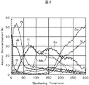
上記特許文献2及び3に記載された拡散バリヤ層として用いられる金属種を参考に、本発明者らは、n型窒化物半導体層上に第一層Al層の厚さを100nmとし、その上に厚さ50nmのMo層、厚さ100nmのTi層、厚さ50nmのPt層の三層構造からなる拡散バリヤ層、そして厚さ300nmのAu層を順次積層した5層構造からなる電極を形成し、窒素雰囲気中で500℃の熱処理を施して、電極表面状態の変化を調べた。その結果、図7に示すように、電極表面に変色を伴う著しい凹凸を有する領域が現れた。
With reference to the metal species used as the diffusion barrier layer described in
この領域について、オージェ電子分光法を用いて分析した結果を図2に示す。
同図より、前記凹凸領域では、電極最下層に存在したはずのAlが電極最表面にまで拡散していることが確認されており、さらにAlと同時に酸素も観測されたことから、電極最表面層は酸化Alが形成されているものと考えられる。
逆に最表面に存在していたAuは半導体方向に拡散していることも確認された。
この凹凸領域は、第一層のAl膜厚のみを30nm程度にまで薄層化した場合でも生じることが確認されており、さらに熱処理温度を上げると、上記変色を伴う凹凸領域は、さらにその面積を拡大することもわかっている。
FIG. 2 shows the result of analyzing this region using Auger electron spectroscopy.
From the figure, it was confirmed that Al, which should have existed in the lowermost layer of the electrode, diffused to the outermost surface of the electrode, and oxygen was also observed at the same time as Al. The layer is considered to be formed of Al oxide.
Conversely, it was also confirmed that Au existing on the outermost surface diffused in the semiconductor direction.
This uneven region has been confirmed to occur even when only the Al film thickness of the first layer is reduced to about 30 nm, and when the heat treatment temperature is further increased, the uneven region with the above discoloration further increases its area. Also knows to expand.
このように酸化したAl領域が電極表面に発生してしまうと、上述した通り実装工程において電極表面とAuワイヤやハンダ材料との間で十分な接合強度が得られなくなるため、素子を実装する上で大きな問題となる。
以上のことから、オーム性取得に必要なAl金属が、Auを最上層とした電極中に存在する場合、半導体製造技術において常識的な膜厚範囲で如何なる拡散バリヤ層を設けようとも、高温の熱処理に伴うAlの拡散を完全に抑えることは困難であるものと予想される。
If the oxidized Al region is generated on the electrode surface as described above, sufficient bonding strength cannot be obtained between the electrode surface and the Au wire or solder material in the mounting process as described above. It becomes a big problem.
From the above, when Al metal necessary for obtaining ohmic properties is present in an electrode having Au as the uppermost layer, no matter what diffusion barrier layer is provided in a film thickness range that is common in semiconductor manufacturing technology, a high temperature is required. It is expected that it is difficult to completely suppress the Al diffusion accompanying the heat treatment.
本発明は、上記問題を解消するべく、n型窒化物半導体に対して良好なオーム性接触が得られ、かつ高温の熱処理に対しても従来のような電極表面荒れを起こさないn電極を備えた窒化物半導体発光装置、及びその製造方法を提供することを目的とする。 In order to solve the above problems, the present invention is provided with an n-electrode that can provide good ohmic contact with an n-type nitride semiconductor and does not cause surface roughness of a conventional electrode even during high-temperature heat treatment. Another object of the present invention is to provide a nitride semiconductor light emitting device and a method for manufacturing the same.
上記問題を解消するためには、Al単体金属を用いなくても、n型窒化物半導体に対して良好なオーム性接触が得られるn電極が必須である。 In order to solve the above problem, an n-electrode that can provide a good ohmic contact with the n-type nitride semiconductor without using an Al single metal is essential.
そこで、本発明の要旨の一例を列挙すれば、次の通りである。
1.基板上に設けられたn型窒化物半導体層と、n型窒化物半導体層上に設けられた所定の波長を有する光を発する活性層と、活性層上に設けられたp型窒化物半導体層と、n型窒化物半導体層と電気的に接続されるn電極と、p型窒化物半導体層と電気的に接続されるp電極とを備え、n電極は、n型窒化物半導体に接する側から順に、窒化アルミニウムからなる厚さが1nm以上、5nm未満の範囲である第一層と、Ti、Zr、Hf、Mo及びPtから選ばれる1以上の金属からなる第二層と、Auからなる第三層とを有する積層構造からなり、前記n電極と前記n型窒化物半導体との間の接続はオーム性であることを特徴とする。
2. 基板上に、少なくともn型不純物が添加されたn型窒化物半導体層を形成する工程と、n型窒化物半導体層上に、所定の波長を有する光を発する活性層を形成する工程と、p型不純物が添加されたp型窒化物半導体層を形成する工程と、p型窒化物半導体上に接してp電極を形成する工程と、n型窒化物半導体上に接して、下から窒化アルミニウムからなる厚さが1nm以上、5nm未満の範囲である第一層を形成する工程と、Ti、Zr、Hf、Mo及びPtから選ばれる1以上の金属からなる第二層と、Auからなる第三層とを有する、前記第一層から第三層までの積層構造からなるn電極を形成する工程と、この後熱処理を施す工程とを具備することを特徴とする。
Then, it will be as follows if an example of the summary of this invention is enumerated.
1. An n-type nitride semiconductor layer provided on a substrate, an active layer emitting light having a predetermined wavelength provided on the n-type nitride semiconductor layer, and a p-type nitride semiconductor layer provided on the active layer And an n-electrode electrically connected to the n-type nitride semiconductor layer, and a p-electrode electrically connected to the p-type nitride semiconductor layer, wherein the n electrode is in contact with the n-type nitride semiconductor In order, the first layer made of aluminum nitride has a thickness of 1 nm or more and less than 5 nm, the second layer made of one or more metals selected from Ti, Zr, Hf, Mo and Pt, and Au. It has a laminated structure having a third layer, and the connection between the n-electrode and the n-type nitride semiconductor is ohmic.
2. Forming an n-type nitride semiconductor layer to which at least an n-type impurity is added on the substrate; forming an active layer emitting light having a predetermined wavelength on the n-type nitride semiconductor layer; and p. Forming a p-type nitride semiconductor layer to which a p-type impurity is added, forming a p-electrode in contact with the p-type nitride semiconductor, and in contact with the n-type nitride semiconductor from below from aluminum nitride Forming a first layer having a thickness of 1 nm or more and less than 5 nm, a second layer made of one or more metals selected from Ti, Zr, Hf, Mo, and Pt, and a third layer made of Au. And a step of forming an n-electrode having a layered structure from the first layer to the third layer, and a step of performing a heat treatment thereafter.
本発明のn電極を用いることで、Al単体金属を用いなくてもn型窒化物半導体に対して良好なオーム性を得ることが可能となり、それと同時にn電極形成後に高温の熱処理を施しても、従来のようなAl拡散が起こらないことから、実装工程において、n電極とAu系ハンダやAuワイヤとの間で、実用上十分な接合強度が得られる。その結果、窒化物半導体発光装置を歩留り良く作製することが可能となる。 By using the n-electrode of the present invention, it becomes possible to obtain good ohmic properties for an n-type nitride semiconductor without using an Al single metal, and at the same time, even if a high-temperature heat treatment is performed after forming the n-electrode. Since conventional Al diffusion does not occur, practically sufficient bonding strength can be obtained between the n-electrode and the Au-based solder or Au wire in the mounting process. As a result, the nitride semiconductor light emitting device can be manufactured with a high yield.
以下に、本発明の一実施形態について、図面を参照しながら説明する。
(実施例1)
図1は、本発明の一実施形態に係る窒化物半導体レーザの断面模式図である。
なお、本発明の主旨はn型窒化物半導体に接して形成されるn電極の構造に関するものであるため、以下で説明するレーザのエピタキシャル成長層の構成は、ごく一般的な積層構成を例に示しているものであって、これに限定されるものではない。
An embodiment of the present invention will be described below with reference to the drawings.
Example 1
FIG. 1 is a schematic cross-sectional view of a nitride semiconductor laser according to an embodiment of the present invention.
Since the gist of the present invention relates to the structure of the n-electrode formed in contact with the n-type nitride semiconductor, the structure of the epitaxially grown layer of the laser described below shows a very general stacked structure as an example. However, the present invention is not limited to this.
以下に窒化物半導体レーザの全体的な製造方法を説明する。
n型GaN基板1上に、SiドープGaNからなるn型バッファ層2、SiドープAlGaNからなるn型クラッド層3、SiドープGaNからなるn型ガイド層4、InGaN多重量子井戸構造からなる活性層5、MgドープAlGaN(Al組成比=7%)からなる電子ブロック層6、MgドープAlGaN(Al組成比=4%)からなるp型クラッド層7、及びMgドープGaNからなるp型コンタクト層8を、一般的な有機金属気相成長法を用いて順次成長させる。
The overall manufacturing method of the nitride semiconductor laser will be described below.
An n-
次に周知のホトリソグラフィ技術と、例えば塩素系ガスを用いたドライエッチング法を用いて、レジストパターンによって開口された基板表面の所望の領域をp型クラッド層7の途中まで、具体的にはp型クラッド層7を30〜40nm程度残す深さまでエッチングして、p型コンタクト層8を最頂部とする共振器幅1.5μmのリッジを形成する。
Next, using a well-known photolithography technique and a dry etching method using, for example, a chlorine-based gas, a desired region of the substrate surface opened by the resist pattern is partway through the p-
次に、基板全面にCVD法、スパッタ法等の周知の絶縁膜形成技術を用いて、例えば膜厚=250nmのSiO2膜9を形成した後、ホトリソグラフィ技術を用いて、上記リッジ最上部に位置する領域のみが開口されたホトレジストパターンを形成し、このホトレジストパターンをエッチングマスクとして上記開口部をエッチングして、リッジ最頂部のp型コンタクト層8を露出させる。
この時エッチング方法としては、フッ酸系薬液を用いたウェットエッチングの他、CF4等のフッ素系ガスを用いたドライエッチング等の周知の技術を用いて行う。
Next, a well-known insulating film forming technique such as CVD or sputtering is formed on the entire surface of the substrate, for example, a SiO 2 film 9 having a film thickness of 250 nm is formed, and then the top of the ridge is formed using a photolithography technique. A photoresist pattern having an opening only in the region where it is located is formed, and the opening is etched using this photoresist pattern as an etching mask to expose the p-type contact layer 8 at the top of the ridge.
At this time, as an etching method, a known technique such as wet etching using a hydrofluoric acid chemical solution or dry etching using a fluorine-based gas such as CF 4 is used.
次に、上記開口されたリッジ最頂部を含む所望の領域を開口する形でホトレジストパターンを形成した後、例えば真空蒸着法を用いて該基板1の表面側全面にNi(ニッケル)膜、Mo(モリブデン)膜、及びAu(金)膜を順次被着し、周知のリフトオフ法を用いて不要な金属膜とホトレジストパターンを除去することで、リッジ最頂部のp型コンタクト層8上、及びその周辺に形成されたSiO2膜上の所望の領域にNi/Mo/Auからなるp電極10が形成される。
Next, after forming a photoresist pattern so as to open a desired region including the top of the opened ridge, a Ni (nickel) film, Mo (Mo Molybdenum) film and Au (gold) film are sequentially deposited, and unnecessary metal film and photoresist pattern are removed using a known lift-off method, so that the p-type contact layer 8 at the top of the ridge and its periphery are removed. A p-
次に、n型GaN基板1の裏面側から、周知の研磨技術を用いて基板厚が約100μm程度の厚さになるまで研磨・薄層化する。
次に、研磨・薄層化されたn型GaN基板1の裏面側全面に、スパッタ法を用いて厚さが3nmの窒化アルミニウム膜(AlN)101を被着した後、例えば電子ビーム蒸着法を用いて厚さが50nmのTi(チタン)膜102、厚さが50nmのPt(白金)膜103、及び厚さが500nmのAu(金)膜104を順次被着する。この後、窒素中で500℃、10分間のアニール処理を施すことで、n型GaN基板1に対してオーム性接触する、下からAlN/Ti/Pt/Auの4層構造からなるn電極11が形成される。
次に、リッジの長手方向と垂直に、例えば600μm程度の長さになるように劈開してバー状の両共振器端面を形成し、両端面に所望の反射率並びに透過率を有する端面コーティング膜12を形成する。
Next, polishing and thinning are performed from the back side of the n-
Next, an aluminum nitride film (AlN) 101 having a thickness of 3 nm is deposited on the entire back surface of the polished and thinned n-
Next, the end face coating film is formed by cleaving to form a length of about 600 μm perpendicular to the longitudinal direction of the ridge to form both bar-shaped resonator end faces, and having desired reflectance and transmittance on both end faces.
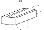
続いて、上記バーを劈開などによりチップ化することで図1の断面構造、並びに図5の形状を有する窒化物半導体レーザが完成し、これをダイボンディングにより前記レーザチップのp電極側をマウント面として、AuSnハンダが塗布されたSiCからなるサブマウント上にマウントし、さらにレーザチップがマウントされたサブマウントを、ステム上にマウントする。最後に上方を向いているレーザチップのn電極面、及びp電極が電気的に接続されたサブマウント上の電極面に、適宜Auワイヤをボンディングして配線することで窒化物半導体レーザ装置が完成する。 Subsequently, the bar is formed into a chip by cleaving or the like to complete the nitride semiconductor laser having the cross-sectional structure of FIG. 1 and the shape of FIG. 5, and the p-electrode side of the laser chip is mounted on the mounting surface by die bonding. Are mounted on a submount made of SiC coated with AuSn solder, and a submount mounted with a laser chip is mounted on the stem. Finally, a nitride semiconductor laser device is completed by appropriately bonding Au wires to the n-electrode surface of the laser chip facing upward and the electrode surface on the submount to which the p-electrode is electrically connected. To do.
前記の工程により窒化物半導体レーザ装置を50個作製するにあたり、n電極面へのAuワイヤボンディングを行う過程での接続不良は一つも発生せず、接続部の外観も良好であった。
これらについて、Auワイヤとn電極表面との接着性を評価するため、n電極表面に接続されたAuワイヤに対して引っ張り試験(ワイヤプルテスト)を行ったところ、断線強度は50個中全て5g以上であり、断線部は全てAuワイヤ途中での断線であることを確認した。
When 50 nitride semiconductor laser devices were manufactured by the above process, no connection failure occurred in the process of Au wire bonding to the n-electrode surface, and the appearance of the connection part was good.
For these, in order to evaluate the adhesion between the Au wire and the n-electrode surface, a tensile test (wire pull test) was performed on the Au wire connected to the n-electrode surface. As described above, it was confirmed that all the disconnected portions were disconnected in the middle of the Au wire.
さらに、前記それぞれのAuワイヤが接続された外部導入端子を介してレーザの電流−電圧(I−V)特性を評価した結果についても、直列抵抗が著しく高いものや立ち上がり電圧などにバラツキは見られず、電極−Auワイヤ間の導通も良好であることを確認した。 Furthermore, the results of evaluating the current-voltage (IV) characteristics of the laser through the external lead-in terminals connected to the respective Au wires also show variations in the series resistance and the rising voltage. In addition, it was confirmed that conduction between the electrode and the Au wire was also good.
上記本実施の形態によるn電極の構造、作用、並びに効果について、本発明者らが行った実験結果に基づき以下に説明する。
実験には、有機金属気相成長法により、サファイア基板上にGaNからなる低温バッファ層と、膜厚=5000nmのアンドープGaN層と、SiドープGaN(ドーピング濃度=1.0〜2.0×1018cm−3、膜厚=1000nm)層をエピタキシャル成長したものを用いた。
そして上記窒化物半導体レーザの作製手法を用いて、オーミック特性の評価方法としては一般的なTLM(Transmission Line Model)パターンを、ホトレジストにより形成することで、電極形成前の試料が完成する。
The structure, operation, and effect of the n-electrode according to the present embodiment will be described below based on the results of experiments conducted by the present inventors.
In the experiment, a low-temperature buffer layer made of GaN on a sapphire substrate, an undoped GaN layer having a film thickness = 5000 nm, and a Si-doped GaN (doping concentration = 1.0 to 2.0 × 10 18 cm −3 , Film thickness = 1000 nm) was used by epitaxially growing the layer.
Then, by using the nitride semiconductor laser fabrication method, a general TLM (Transmission Line Model) pattern is formed of photoresist as a method for evaluating ohmic characteristics, thereby completing a sample before electrode formation.
前記SiドープGaN層からなるTLMパターンのメサ幅(=電極幅)は100μmであり、メサエッチングによって形成した台地の表面には、電極間隔が20、40、80、160、320μmとなるようにn電極を被着するためのホトレジスト開口部を配置した。
この試料に対して、電極最下層となる窒化アルミニウムを、スパッタ法により膜厚をそれぞれ3nm、5nm、8nmの3条件とした3種類の試料を作製する。この時、特に基板加熱は行っていない。
The mesa width (= electrode width) of the TLM pattern made of the Si-doped GaN layer is 100 μm, and the surface of the platen formed by mesa etching is n, so that the electrode spacing is 20, 40, 80, 160, 320 μm. A photoresist opening for depositing the electrode was placed.
With respect to this sample, three types of samples having aluminum nitride as the lowermost layer of the electrode and having film thicknesses of 3 nm, 5 nm, and 8 nm, respectively, are prepared by sputtering. At this time, the substrate is not particularly heated.
この3試料と窒化アルミニウムを被着していない試料(1試料)を加えた4試料に対して、重ねて膜厚50nmのTi(チタン)層、膜厚50nmのPt(白金)層、及び膜厚300nmのAu(金)層を電子ビーム蒸着法により積層形成して、この後周知のリフトオフ法によりホトレジストとともに、不要な金属膜、及び窒化アルミニウム膜を除去することで、TLM測定試料が完成する。 A stack of 50 nm-thick Ti (titanium) layer, 50 nm-thickness Pt (platinum) layer, and a film over these four samples plus four samples with no aluminum nitride coating (one sample) A 300 nm thick Au (gold) layer is formed by electron beam evaporation, and then the TLM measurement sample is completed by removing the unnecessary metal film and aluminum nitride film together with the photoresist by a known lift-off method. .
この4試料に対して、窒素雰囲気中で400℃〜550℃の温度範囲で熱処理した時の、電極間隔=20μmにおける電極間I−V特性を評価した結果を図3A〜Dに示す。 3A to 3D show the results of evaluating the IV characteristics between the electrodes when the electrode spacing was 20 μm when the four samples were heat-treated in a nitrogen atmosphere at a temperature range of 400 ° C. to 550 ° C.
図3Aは、窒化アルミニウムの無いTi/Pt/Au電極のみの特性を示しており、図3B、C、Dは、最下層の窒化アルミニウム(以降、積層構造を表す際にはAlNと略す)膜厚をそれぞれ3nm、5nm、8nmとし、その上にTi/Pt/Auを重ねて形成した電極の特性を示している。 FIG. 3A shows the characteristics of only a Ti / Pt / Au electrode without aluminum nitride, and FIGS. 3B, 3C, and 3D show the lowermost aluminum nitride film (hereinafter abbreviated as AlN when representing a laminated structure). The graph shows the characteristics of an electrode formed by stacking Ti / Pt / Au on the thicknesses of 3 nm, 5 nm, and 8 nm, respectively.
それぞれの電極の特性について、以下に説明する。
図3AのTi/Pt/Au電極のみの場合では、熱処理前において非オーム性ではあるものの、電圧の増加に伴う僅かな電流増加が見られたが、400℃以上の熱処理を施すことで、殆ど電流が流れなくなってしまった。
図3BのAlN(3nm)/Ti/Pt/Au電極では、熱処理前の段階では電流の増加は確認されなかったが、400℃以上の熱処理によって比較的良好なオーム性を示すようになり、450℃〜500℃熱処理後において、最も良好なI−V特性を示した。図示していないが、600℃熱処理後においても、ρc<1.0×10−4Ωcm2であり、電極表面も光沢面から僅かな凹凸に起因した曇り面に変化したが、従来のような著しい変色領域は確認されず良好なAu色が保持されていることを確認した。
図3CのAlN(5nm)/Ti/Pt/Au電極では、熱処理前〜400℃熱処理後まで電流の増加は見られず、450℃以上の熱処理でオーム性が得られはじめ、500℃〜550℃熱処理後に最も良好なI−V特性を示したが、前記(b)と比較して電流値は小さい。
図3DのAlN(8nm)/Ti/Pt/Au電極では、熱処理前〜450℃熱処理後まで電流の増加は見られず、500℃熱処理後にようやくオーム性を示し始めたが、550℃熱処理後においても、前記(b)、(c)と比較して大きな電流値は得られていない。
The characteristics of each electrode will be described below.
In the case of only the Ti / Pt / Au electrode of FIG. 3A, although it was non-ohmic before the heat treatment, a slight current increase with an increase in voltage was observed, but by applying the heat treatment at 400 ° C. or higher, The current stopped flowing.
In the AlN (3 nm) / Ti / Pt / Au electrode of FIG. 3B, no increase in current was confirmed before the heat treatment, but a relatively good ohmic property was exhibited by the heat treatment at 400 ° C. or higher. The best IV characteristics were exhibited after the heat treatment at from 500C to 500C. Although not shown, even after heat treatment at 600 ° C., ρc <1.0 × 10 −4 Ωcm 2 , and the electrode surface was also changed from a glossy surface to a cloudy surface due to slight irregularities, but a significant discoloration as in the past The region was not confirmed and it was confirmed that a good Au color was retained.
In the AlN (5 nm) / Ti / Pt / Au electrode of FIG. 3C, no increase in current was observed before the heat treatment until after the heat treatment at 400 ° C., and ohmic properties began to be obtained after the heat treatment at 450 ° C. or higher. Although the best IV characteristics were shown after the heat treatment, the current value was smaller than that of (b).
In the AlN (8 nm) / Ti / Pt / Au electrode of FIG. 3D, no increase in current was observed from before the heat treatment to after the 450 ° C. heat treatment, and finally began to show ohmic properties after the 500 ° C. heat treatment. However, a large current value is not obtained as compared with the cases (b) and (c).
これらのI−V特性から求めた抵抗値を用いて算出した比接触抵抗ρcの熱処理温度依存性を評価した結果を図4に示す。
同図中の特性線1(AlN膜厚=3nm)、特性線2(AlN膜厚=5nm)、特性線3(AlN膜厚=8nm)から判るように、窒化アルミニウムの膜厚が厚ければ厚いほどρcは高くなる傾向にあり、前記I−V特性評価結果と合わせて、レーザ素子等の発光素子に適用できるオーム性を得るためには、窒化アルミニウムの膜厚は、厚くても5nmまでであることがわかった。
逆に窒化アルミニウムが薄ければ薄いほど良好なオーム性が得られるものと推測されるが、前記の実験結果によれば、窒化アルミニウムが全く無い場合はオーム性を示さない。
FIG. 4 shows the results of evaluating the heat treatment temperature dependence of the specific contact resistance ρc calculated using the resistance values obtained from these IV characteristics.
As can be seen from the characteristic line 1 (AlN film thickness = 3 nm), characteristic line 2 (AlN film thickness = 5 nm), and characteristic line 3 (AlN film thickness = 8 nm) in FIG. Ρc tends to increase as the thickness increases, and in combination with the IV characteristic evaluation results, in order to obtain ohmic properties applicable to light-emitting elements such as laser elements, the film thickness of aluminum nitride can be as large as 5 nm. I found out that
On the contrary, it is presumed that the thinner the aluminum nitride is, the better the ohmic property is obtained. However, according to the above experimental results, the ohmic property is not exhibited when there is no aluminum nitride.
従って、被着形成した窒化アルミニウムの膜厚下限としては、一般的な手法による膜厚評価の限界である1nm前後の厚さと考えられるが、例えば膜ではなく島状に薄く窒化アルミニウムが存在するだけでも、オーム性向上に効果があるものと考えられる。 Therefore, the lower limit of the film thickness of the deposited aluminum nitride is considered to be a thickness of around 1 nm, which is the limit of the film thickness evaluation by a general method. However, it is thought that it is effective for improving ohmic properties.
次に、前記実験において最も特性の良かったAlN(膜厚=3nm)/Ti/Pt/Au電極について、熱処理前と500℃熱処理後の積層構造の変化を、断面TEM観察とEDX面分析によって調べた。その結果、500℃熱処理後においても第一層の窒化アルミニウムに大幅な変化は見られず、その存在が明瞭に観察されており、さらにその上層のTi/Pt/Auもそれぞれの界面において僅かな相互拡散が見られた以外は、当初の積層状態を保持していることが観察された。 Next, regarding the AlN (film thickness = 3 nm) / Ti / Pt / Au electrode with the best characteristics in the experiment, the change in the laminated structure before the heat treatment and after the heat treatment at 500 ° C. was examined by cross-sectional TEM observation and EDX plane analysis. It was. As a result, even after the heat treatment at 500 ° C., no significant change was observed in the aluminum nitride of the first layer, its existence was clearly observed, and Ti / Pt / Au of the upper layer was also slightly at each interface. It was observed that the original laminated state was maintained except that interdiffusion was observed.
以上のことから、Al単体金属を用いずにn型窒化物半導体に対してオーム性接触を得るためには、n型窒化物半導体とAl以外の金属膜との間に膜厚を規定した窒化アルミニウムを存在させることが重要であり、この窒化アルミニウムの形成方法として前記実験に用いたスパッタ法で場合でも、この後金属膜を重ねて被着形成し、前記実験結果から少なくとも400℃〜600℃の熱処理を施すことで、n型窒化物半導体に対して良好なオーム性接触を得ることが可能となる上、熱処理に伴う電極最表面側への異種金属拡散の無い実装工程に適したAu最表面も保持できる。 From the above, in order to obtain ohmic contact with an n-type nitride semiconductor without using an Al single metal, nitriding with a prescribed thickness between the n-type nitride semiconductor and a metal film other than Al It is important that aluminum is present, and even when the sputtering method used in the experiment as a method of forming the aluminum nitride, a metal film is formed after deposition, and from the experimental result, at least 400 ° C. to 600 ° C. By performing this heat treatment, it is possible to obtain a good ohmic contact with the n-type nitride semiconductor, and the Au outermost layer suitable for a mounting process in which no different metal diffuses to the electrode outermost surface side due to the heat treatment. The surface can also be retained.
上記実験結果によれば、ある熱処理温度を境にしてI−V特性に顕著な変化が見られること、500℃熱処理後の窒化アルミニウム膜に大幅な変化が見られないことから鑑みて、形成直後にはn型窒化物半導体上にただ堆積していただけの結晶性の低い窒化アルミニウム膜が、熱処理を施すことでn型窒化物半導体と結晶的に結合してヘテロ界面が形成され、これによってn型窒化物半導体と窒化アルミニウム上の金属膜との間で、トンネル効果によるオーム性接触が実現されたものと考えられる。これは、前記実験においてGaNよりもバンドギャップの大きい窒化アルミニウムの膜厚が厚いほど、n電極間の抵抗値が増大する傾向を示すことからも予測されうることである。 According to the above experimental results, in view of the remarkable change in IV characteristics at a certain heat treatment temperature and the fact that there is no significant change in the aluminum nitride film after the 500 ° C. heat treatment, In this case, an aluminum nitride film having low crystallinity, which has only been deposited on the n-type nitride semiconductor, is crystallized with the n-type nitride semiconductor by heat treatment to form a hetero interface. It is considered that ohmic contact by the tunnel effect is realized between the type nitride semiconductor and the metal film on the aluminum nitride. This can be predicted from the fact that the resistance value between the n-electrodes tends to increase as the film thickness of aluminum nitride having a larger band gap than GaN increases in the experiment.
逆に、MOVPE法等の通常の結晶成長法で窒化アルミニウムを成長させるには1200℃以上の基板加熱が必要であるため、前記のような基板表面側に金属膜が形成されている状態、さらに基板が薄層化されている状態に対しては、成長炉内の金属汚染や、基板が割れてしまう等の様々な悪影響を及ぼす危険性が高いため、現実的に選択できる方法ではない。
さらにIn(インジウム)が含まれる活性層が形成された基板に対して、1200℃以上の熱処理を施すと、Inの拡散・偏析等が生じて活性層が壊れてしまう危険性もある。
On the contrary, in order to grow aluminum nitride by a normal crystal growth method such as MOVPE method, it is necessary to heat the substrate at 1200 ° C. or higher, so that the metal film is formed on the substrate surface side as described above, Since the substrate is thinned, there is a high risk of various adverse effects such as metal contamination in the growth furnace and cracking of the substrate.
Further, if a substrate on which an active layer containing In (indium) is formed is subjected to heat treatment at 1200 ° C. or higher, there is a risk that the active layer is broken due to In diffusion and segregation.
本発明では、半導体製造プロセスで一般的なスパッタ法等の成膜方法を用いて形成した窒化アルミニウムでも、前記のような作用、効果が得られることに特徴があり、前記スパッタ法以外にも、CVD法、昇華法等、半導体プロセスで一般的な手法を用いて形成しても良い。
また、窒化アルミニウム上に形成する電極金属についても、先に述べたオーム性が得られる推測原理から考えて、窒化アルミニウムに対して接着する金属であれば、如何なる金属材料、または導電性金属酸化物等の金属化合物材料を用いても良い。
(実施例2)
図6は、本発明の他の実施形態に係る窒化物半導体発光ダイオード(LED)の模式図である。以下に全体的な製造方法を説明する。
サファイア基板20上に、アンドープGaNからなるバッファ層21と、キャリア濃度=2×1018cm−3で膜厚=5μmのSiドープn型GaN層22、Siドープn型AlGaNクラッド層23、InbGa1−bN(0<b≦0.1)からなる活性層24と、Mgドーピング濃度=3.0×1019cm−3で膜厚=40nmのMgドープAlGaNからなるp型クラッド層25、及びMgドープGaNからなるp型コンタクト層26からなる多層構造を、有機金属気相成長法を用いて順次成長させる。
次に、周知のホトリソグラフィ技術と塩素系ガスを用いたドライエッチング法により、該基板20表面側から所望の領域をエッチングして、Siドープn型GaN層22を露出させる。
In the present invention, aluminum nitride formed by using a film forming method such as a general sputtering method in a semiconductor manufacturing process is characterized in that the above operation and effect can be obtained. You may form using a general method in semiconductor processes, such as CVD method and a sublimation method.
In addition, regarding the electrode metal formed on aluminum nitride, any metal material or conductive metal oxide can be used as long as it is a metal that adheres to aluminum nitride in view of the above-described presumed principle of obtaining ohmic properties. A metal compound material such as
(Example 2)
FIG. 6 is a schematic view of a nitride semiconductor light emitting diode (LED) according to another embodiment of the present invention. The overall manufacturing method will be described below.
On the
Next, a desired region is etched from the surface side of the
次に、露出したSiドープn型GaN層22の所望の位置に、スパッタ法を用いて膜厚が1.5nmの窒化アルミニウム膜(AlN)201を被着した後、さらにその上に膜厚が30nmのHf(ハフニウム)膜202、膜厚が50nmのMo(モリブデン)膜203、膜厚が100nmのZr(ジルコニウム)膜204、膜厚が100nmのPt(白金)層205、及び膜厚が500nmのAu(金)膜206を、電子ビーム蒸着法を用いて積層形成し、窒素雰囲気中において450℃のアニール処理を施すことで、SiドープN型GaN層22に対してオーム性接触するAlN/Hf/Mo/Zr/Pt/Auの6層構造からなるn電極27が形成される。
Next, an aluminum nitride film (AlN) 201 having a film thickness of 1.5 nm is deposited on a desired position of the exposed Si-doped n-type GaN layer 22 by sputtering, and then a film thickness of 30 nm is further formed thereon. Hf (hafnium)
次に、上記エッチング工程でエッチングされなかった領域の、第二のp型クラッド層26上の所望の位置に、膜厚が30nmのPd(パラジウム)膜/膜厚が70nmのPt(白金)膜/膜厚が300nmのAu(金)膜を積層形成することにより、p電極28が形成される。
この時、n電極27の最表面とp電極28の最表面は、ほぼ同じ高さとなるような膜厚構成をとっている。
この後、サファイア基板20の裏面側を、ダイヤモンド砥粒等を用いて厚さが200μm程度になるまで薄層化し、最終処理として研磨面を鏡面に仕上げ、所望も大きさにチップ化することで、窒化物半導体発光ダイオード(LED)が完成する。
Next, a Pd (palladium) film having a film thickness of 30 nm / a Pt (platinum) film having a film thickness of 70 nm at a desired position on the second p-
At this time, the outermost surface of the n-
After that, the back side of the
前記LEDはサファイア基板を通して、鏡面研磨された裏面側から放出される光を利用するものであるため、LEDを実装するマウント上には、予めAu−Snハンダによるパターニングが施されており、パターニングされたAu−Snハンダに対して、p、n各々の電極と、対応するAu−Snハンダパターンとを合わせる形で実装する。
前記の工程によりLED装置を30個作製し、外部導入端子を介してLEDのI−V特性を評価した結果、50mAの電流値を得るために要した電圧の平均値は3.25Vであり、著しく電圧の高いものや、電流が得られないものは一つも無かった。
さらに、実装したLEDチップに対してせん断強度試験を行った結果、全て400g以上のせん断強度を有していることもわかり、実装工程で何ら問題が発生していないことも確認した。
以上の実施例では、基板材料としてサファイア基板を適用した例について述べたが、常識的に窒化物半導体が成長しうる基板材料、例えばGaN、SiC、Si等でも良く、製造するLEDの構造により如何なる基板材料を用いても良いことは言うまでも無い。
Since the LED uses light emitted from the back side that has been mirror-polished through a sapphire substrate, patterning with Au-Sn solder has been performed on the mount for mounting the LED in advance. The Au-Sn solder is mounted in such a manner that the electrodes of p and n are matched with the corresponding Au-Sn solder pattern.
As a result of producing 30 LED devices by the above process and evaluating the IV characteristics of the LED through the external lead-in terminal, the average value of the voltage required to obtain a current value of 50 mA is 3.25 V. There was no one with high voltage or no current.
Furthermore, as a result of conducting a shear strength test on the mounted LED chip, it was found that all had a shear strength of 400 g or more, and it was confirmed that no problems occurred in the mounting process.
In the above embodiments, an example in which a sapphire substrate is applied as a substrate material has been described. However, a common substrate material on which a nitride semiconductor can be grown, such as GaN, SiC, Si, etc., may be used depending on the structure of the LED to be manufactured. Needless to say, a substrate material may be used.
以上の実施例では、n電極における窒化アルミニウムとAuとの金属膜として、下からTi/Pt積層膜、及びHf/Mo/Zr/Pt積層膜を用いた例について述べたが、これに限定されることはなく、Auワイヤ、Au−Snハンダ等の接着させる材料ごとに、適切に金属積層体、及び膜厚を変えても良いことは言うまでも無い。
以上、本発明の実施形態について、各窒化物半導体発光素子の製造方法を交えながら詳述してきたが、具体的な窒化物半導体層の構成は本実施形態に限定されるものではなく、作製するデバイスの構造や必要とされる性能に応じて、種々変更可能である。
In the above embodiment, the example using the Ti / Pt laminated film and the Hf / Mo / Zr / Pt laminated film from the bottom as the metal film of aluminum nitride and Au in the n electrode has been described. However, the present invention is not limited to this. Needless to say, the metal laminate and the film thickness may be appropriately changed for each material to be bonded, such as an Au wire and Au—Sn solder.
As described above, the embodiment of the present invention has been described in detail with the manufacturing method of each nitride semiconductor light emitting element, but the specific configuration of the nitride semiconductor layer is not limited to this embodiment and is manufactured. Various changes can be made according to the structure of the device and the required performance.
以上のことから、本発明のn電極を窒化物半導体発光素子に適用することで、n型窒化物半導体に対して良好なオーム性接触が得られ、かつ高温の熱処理を施した後でも、実装工程に適したAuからなるn電極最表面を良好に保持することができる。 From the above, by applying the n-electrode of the present invention to a nitride semiconductor light emitting device, good ohmic contact can be obtained with respect to the n-type nitride semiconductor, and even after a high-temperature heat treatment is applied. The outermost surface of the n electrode made of Au suitable for the process can be satisfactorily maintained.
1…n型GaN基板、
2…n型バッファ層、
3…n型クラッド層、
4…n型ガイド層、
5…活性層、
6…電子ブロック層、
7…p型クラッド層、
8…p型コンタクト層、
9…SiO2膜、
10…p電極、
101…窒化アルミニウム膜、
102…Ti膜、
103…Pt膜、
104…Au膜、
11…n電極、
12…端面コーティング膜、
20…サファイア基板、
21…アンドープGaNからなるバッファ層、
22…n型GaN層、
23…n型AlGaNクラッド層、
24…活性層、
25…p型クラッド層、
26…p型コンタクト層、
201…窒化アルミニウム膜、
202…Hf膜、
203…Mo膜、
204…Zr膜、
205…Pt膜、
206…Au膜
27…n電極、
28…p電極。
1 ... n-type GaN substrate,
2 ... n-type buffer layer,
3 ... n-type cladding layer,
4 ... n-type guide layer,
5 ... active layer,
6 ... electronic block layer,
7 ... p-type cladding layer,
8 ... p-type contact layer,
9 ... SiO 2 film,
10 ... p electrode,
101 ... Aluminum nitride film,
102 ... Ti film,
103 ... Pt film,
104 ... Au film,
11 ... n electrode,
12… End face coating film,
20 ... Sapphire substrate,
21 ... a buffer layer made of undoped GaN,
22 n-type GaN layer,
23 ... n-type AlGaN cladding layer,
24 ... active layer,
25 ... p-type cladding layer,
26 ... p-type contact layer,
201 ... Aluminum nitride film,
202 ... Hf film,
203 ... Mo film,
204 ... Zr film,
205 ... Pt film,
206… Au film
27 ... n electrode,
28 ... p electrode.
Claims (10)
前記n型窒化物半導体層上に設けられた所定の波長を有する光を発する発光層と、
前記発光層上に設けられたp型窒化物半導体層と、
前記n型窒化物半導体層と電気的に接続されたn電極と、
前記p型窒化物半導体層と電気的に接続されたp電極とを備え、
前記n電極は、前記n型窒化物半導体層に近い側から順に第1層、第2層、第3層とがそれぞれ積層された積層膜であり、
前記第1層は、厚さが1nm以上、5nm以下の範囲を有する窒化アルミニウムからなり、
前記第2層は、Ti、Zr、Hf、Mo及びPtから選ばれる1以上の金属からなり、
前記第3層は、Auからなることを特徴とする窒化物半導体発光装置。 an n-type nitride semiconductor layer;
A light emitting layer that emits light having a predetermined wavelength provided on the n-type nitride semiconductor layer;
A p-type nitride semiconductor layer provided on the light emitting layer;
An n-electrode electrically connected to the n-type nitride semiconductor layer;
A p-electrode electrically connected to the p-type nitride semiconductor layer,
The n electrode is a laminated film in which a first layer, a second layer, and a third layer are laminated in order from the side close to the n-type nitride semiconductor layer,
The first layer is made of aluminum nitride having a thickness of 1 nm or more and 5 nm or less,
The second layer is made of one or more metals selected from Ti, Zr, Hf, Mo and Pt,
The nitride semiconductor light emitting device, wherein the third layer is made of Au.
前記発光層上に、少なくともp型不純物が添加されたp型窒化物半導体層を形成する工程と、
前記p型窒化物半導体上にp電極を形成する工程と、
前記n型窒化物半導体層の一表面上に、前記n型窒化物半導体層に近い側から順に窒化アルミニウムからなる厚さが1nm以上、5nm以下の範囲である第1層と、Ti、Zr、Hf、Mo及びPtから選ばれる1以上の金属からなる第2層と、Auからなる第3層とのそれぞれを積層する工程と、
前記積層する工程の後に、前記n型窒化物半導体層に熱処理を施す工程とを具備することを特徴とする窒化物半導体発光装置の製造方法。 forming a light emitting layer emitting light having a predetermined wavelength on the n-type nitride semiconductor layer;
Forming a p-type nitride semiconductor layer to which at least a p-type impurity is added on the light emitting layer;
Forming a p-electrode on the p-type nitride semiconductor;
On one surface of the n-type nitride semiconductor layer, a first layer having a thickness of 1 nm or more and 5 nm or less in order from the side closer to the n-type nitride semiconductor layer, Ti, Zr, Laminating each of a second layer made of one or more metals selected from Hf, Mo and Pt and a third layer made of Au;
And a step of performing a heat treatment on the n-type nitride semiconductor layer after the step of laminating.
Priority Applications (3)
| Application Number | Priority Date | Filing Date | Title |
|---|---|---|---|
| JP2008035868A JP5085369B2 (en) | 2008-02-18 | 2008-02-18 | Nitride semiconductor light emitting device and manufacturing method thereof |
| US12/193,992 US20090206360A1 (en) | 2008-02-18 | 2008-08-19 | Nitride semiconductor light emitting device and method of manufacturing the same |
| US13/478,024 US8686442B2 (en) | 2008-02-18 | 2012-05-22 | Nitride semiconductor light emitting device and method of manufacturing the same |
Applications Claiming Priority (1)
| Application Number | Priority Date | Filing Date | Title |
|---|---|---|---|
| JP2008035868A JP5085369B2 (en) | 2008-02-18 | 2008-02-18 | Nitride semiconductor light emitting device and manufacturing method thereof |
Publications (3)
| Publication Number | Publication Date |
|---|---|
| JP2009194295A JP2009194295A (en) | 2009-08-27 |
| JP2009194295A5 JP2009194295A5 (en) | 2010-11-18 |
| JP5085369B2 true JP5085369B2 (en) | 2012-11-28 |
Family
ID=40954273
Family Applications (1)
| Application Number | Title | Priority Date | Filing Date |
|---|---|---|---|
| JP2008035868A Expired - Fee Related JP5085369B2 (en) | 2008-02-18 | 2008-02-18 | Nitride semiconductor light emitting device and manufacturing method thereof |
Country Status (2)
| Country | Link |
|---|---|
| US (2) | US20090206360A1 (en) |
| JP (1) | JP5085369B2 (en) |
Families Citing this family (6)
| Publication number | Priority date | Publication date | Assignee | Title |
|---|---|---|---|---|
| JP5526712B2 (en) * | 2009-11-05 | 2014-06-18 | 豊田合成株式会社 | Semiconductor light emitting device |
| US8716743B2 (en) * | 2012-02-02 | 2014-05-06 | Epistar Corporation | Optoelectronic semiconductor device and the manufacturing method thereof |
| US9099623B2 (en) | 2013-08-30 | 2015-08-04 | Taiwan Semiconductor Manufacturing Company, Ltd. | Manufacture including substrate and package structure of optical chip |
| US9419156B2 (en) * | 2013-08-30 | 2016-08-16 | Taiwan Semiconductor Manufacturing Co., Ltd. | Package and method for integration of heterogeneous integrated circuits |
| JP7146589B2 (en) * | 2018-11-15 | 2022-10-04 | 日機装株式会社 | Semiconductor light emitting device and method for manufacturing semiconductor light emitting device |
| CN112795871A (en) * | 2020-12-25 | 2021-05-14 | 至芯半导体(杭州)有限公司 | Preparation method of AlN thin film |
Family Cites Families (16)
| Publication number | Priority date | Publication date | Assignee | Title |
|---|---|---|---|---|
| JPH04253378A (en) * | 1991-01-29 | 1992-09-09 | Sanyo Electric Co Ltd | Manufacture of photovoltaic device |
| KR100286699B1 (en) * | 1993-01-28 | 2001-04-16 | 오가와 에이지 | Gallium Nitride Group 3-5 Compound Semiconductor Light-Emitting Device and Manufacturing Method Thereof |
| JP2783349B2 (en) | 1993-07-28 | 1998-08-06 | 日亜化学工業株式会社 | Electrode of n-type gallium nitride-based compound semiconductor layer and method of forming the same |
| US6542526B1 (en) * | 1996-10-30 | 2003-04-01 | Hitachi, Ltd. | Optical information processor and semiconductor light emitting device suitable for the same |
| US6459100B1 (en) * | 1998-09-16 | 2002-10-01 | Cree, Inc. | Vertical geometry ingan LED |
| ATE452445T1 (en) * | 1999-03-04 | 2010-01-15 | Nichia Corp | NITRIDE SEMICONDUCTOR LASER ELEMENT |
| JP3587081B2 (en) * | 1999-05-10 | 2004-11-10 | 豊田合成株式会社 | Method of manufacturing group III nitride semiconductor and group III nitride semiconductor light emitting device |
| JP2004140052A (en) * | 2002-10-16 | 2004-05-13 | Sanyo Electric Co Ltd | Electrode structure and its fabricating process |
| JP2004214530A (en) * | 2003-01-08 | 2004-07-29 | Nippon Telegr & Teleph Corp <Ntt> | Method of manufacturing mis compound semiconductor device |
| JP4508534B2 (en) | 2003-01-17 | 2010-07-21 | シャープ株式会社 | Electrode structure for nitride semiconductor and method of manufacturing the same |
| JP4733371B2 (en) | 2004-08-18 | 2011-07-27 | 三菱化学株式会社 | Ohmic electrode for n-type nitride semiconductor and method of manufacturing the same |
| US20060124956A1 (en) * | 2004-12-13 | 2006-06-15 | Hui Peng | Quasi group III-nitride substrates and methods of mass production of the same |
| JP4653671B2 (en) * | 2005-03-14 | 2011-03-16 | 株式会社東芝 | Light emitting device |
| CN101124704A (en) * | 2005-03-16 | 2008-02-13 | 松下电器产业株式会社 | Nitride semiconductor device and method for manufacturing same |
| KR100706952B1 (en) * | 2005-07-22 | 2007-04-12 | 삼성전기주식회사 | VERTICALLY STRUCTURED GaN TYPE LED DEVICE AND METHOD OF MANUFACTURING THE SAME |
| WO2008048303A2 (en) * | 2005-12-12 | 2008-04-24 | Kyma Technologies, Inc. | Group iii nitride articles and methods for making same |
-
2008
- 2008-02-18 JP JP2008035868A patent/JP5085369B2/en not_active Expired - Fee Related
- 2008-08-19 US US12/193,992 patent/US20090206360A1/en not_active Abandoned
-
2012
- 2012-05-22 US US13/478,024 patent/US8686442B2/en active Active
Also Published As
| Publication number | Publication date |
|---|---|
| US20090206360A1 (en) | 2009-08-20 |
| US8686442B2 (en) | 2014-04-01 |
| JP2009194295A (en) | 2009-08-27 |
| US20120228664A1 (en) | 2012-09-13 |
Similar Documents
| Publication | Publication Date | Title |
|---|---|---|
| EP2763192B1 (en) | Nitride semiconductor element and method for producing same | |
| JP4183299B2 (en) | Gallium nitride compound semiconductor light emitting device | |
| US8822976B2 (en) | Nitride semiconductor ultraviolet light-emitting element | |
| US8552455B2 (en) | Semiconductor light-emitting diode and a production method therefor | |
| US9112115B2 (en) | Nitride semiconductor ultraviolet light-emitting element | |
| JP7049186B2 (en) | Manufacturing method of semiconductor light emitting device and semiconductor light emitting device | |
| JP2002016311A (en) | Gallium nitride based light emitting element | |
| US8304802B2 (en) | Nitride-based semiconductor device having electrode on m-plane | |
| US11335830B2 (en) | Photo-emission semiconductor device and method of manufacturing same | |
| TW200830655A (en) | Method for manufacturing semiconductor optical device | |
| JP5085369B2 (en) | Nitride semiconductor light emitting device and manufacturing method thereof | |
| JP2010067858A (en) | Nitride-based semiconductor device and method of manufacturing the same | |
| JPH10173224A (en) | Compound semiconductor light emitting element and its manufacture | |
| JP5098135B2 (en) | Semiconductor laser element | |
| JP2005340860A (en) | Semiconductor light-emitting element | |
| TWI543402B (en) | A light-emitting element, a light-emitting element, and a semiconductor device | |
| JP2008147294A (en) | Electronic device | |
| JP5289791B2 (en) | Nitride semiconductor light emitting device and manufacturing method thereof | |
| JP5132739B2 (en) | Semiconductor element | |
| JP2009021424A (en) | Nitride semiconductor light emitting element, and manufacturing method thereof | |
| US20230034297A1 (en) | Semiconductor light-emitting element | |
| JP4901241B2 (en) | Semiconductor light emitting device and manufacturing method thereof | |
| JP5438534B2 (en) | Semiconductor device and manufacturing method thereof | |
| JP2015153827A (en) | Semiconductor light emitting element and manufacturing method of the same | |
| KR101171855B1 (en) | Supporting substrates for semiconductor light emitting device and high-performance vertical structured semiconductor light emitting devices using supporting substrates |
Legal Events
| Date | Code | Title | Description |
|---|---|---|---|
| A521 | Request for written amendment filed |
Free format text: JAPANESE INTERMEDIATE CODE: A523 Effective date: 20101001 |
|
| A621 | Written request for application examination |
Free format text: JAPANESE INTERMEDIATE CODE: A621 Effective date: 20101001 |
|
| A977 | Report on retrieval |
Free format text: JAPANESE INTERMEDIATE CODE: A971007 Effective date: 20111228 |
|
| A131 | Notification of reasons for refusal |
Free format text: JAPANESE INTERMEDIATE CODE: A131 Effective date: 20120124 |
|
| A521 | Request for written amendment filed |
Free format text: JAPANESE INTERMEDIATE CODE: A523 Effective date: 20120316 |
|
| TRDD | Decision of grant or rejection written | ||
| A01 | Written decision to grant a patent or to grant a registration (utility model) |
Free format text: JAPANESE INTERMEDIATE CODE: A01 Effective date: 20120807 |
|
| A01 | Written decision to grant a patent or to grant a registration (utility model) |
Free format text: JAPANESE INTERMEDIATE CODE: A01 |
|
| A61 | First payment of annual fees (during grant procedure) |
Free format text: JAPANESE INTERMEDIATE CODE: A61 Effective date: 20120905 |
|
| R150 | Certificate of patent or registration of utility model |
Free format text: JAPANESE INTERMEDIATE CODE: R150 Ref document number: 5085369 Country of ref document: JP Free format text: JAPANESE INTERMEDIATE CODE: R150 |
|
| FPAY | Renewal fee payment (event date is renewal date of database) |
Free format text: PAYMENT UNTIL: 20150914 Year of fee payment: 3 |
|
| S531 | Written request for registration of change of domicile |
Free format text: JAPANESE INTERMEDIATE CODE: R313531 |
|
| R350 | Written notification of registration of transfer |
Free format text: JAPANESE INTERMEDIATE CODE: R350 |
|
| S111 | Request for change of ownership or part of ownership |
Free format text: JAPANESE INTERMEDIATE CODE: R313113 |
|
| R350 | Written notification of registration of transfer |
Free format text: JAPANESE INTERMEDIATE CODE: R350 |
|
| R250 | Receipt of annual fees |
Free format text: JAPANESE INTERMEDIATE CODE: R250 |
|
| R250 | Receipt of annual fees |
Free format text: JAPANESE INTERMEDIATE CODE: R250 |
|
| S531 | Written request for registration of change of domicile |
Free format text: JAPANESE INTERMEDIATE CODE: R313531 |
|
| R360 | Written notification for declining of transfer of rights |
Free format text: JAPANESE INTERMEDIATE CODE: R360 |
|
| R350 | Written notification of registration of transfer |
Free format text: JAPANESE INTERMEDIATE CODE: R350 |
|
| R250 | Receipt of annual fees |
Free format text: JAPANESE INTERMEDIATE CODE: R250 |
|
| R250 | Receipt of annual fees |
Free format text: JAPANESE INTERMEDIATE CODE: R250 |
|
| R250 | Receipt of annual fees |
Free format text: JAPANESE INTERMEDIATE CODE: R250 |
|
| R250 | Receipt of annual fees |
Free format text: JAPANESE INTERMEDIATE CODE: R250 |
|
| R250 | Receipt of annual fees |
Free format text: JAPANESE INTERMEDIATE CODE: R250 |
|
| R250 | Receipt of annual fees |
Free format text: JAPANESE INTERMEDIATE CODE: R250 |
|
| LAPS | Cancellation because of no payment of annual fees |