JP5077385B2 - Vehicle navigation device - Google Patents
Vehicle navigation device Download PDFInfo
- Publication number
- JP5077385B2 JP5077385B2 JP2010093945A JP2010093945A JP5077385B2 JP 5077385 B2 JP5077385 B2 JP 5077385B2 JP 2010093945 A JP2010093945 A JP 2010093945A JP 2010093945 A JP2010093945 A JP 2010093945A JP 5077385 B2 JP5077385 B2 JP 5077385B2
- Authority
- JP
- Japan
- Prior art keywords
- backup
- power supply
- control means
- power
- storage means
- Prior art date
- Legal status (The legal status is an assumption and is not a legal conclusion. Google has not performed a legal analysis and makes no representation as to the accuracy of the status listed.)
- Expired - Fee Related
Links
Images


Classifications
-
- G—PHYSICS
- G01—MEASURING; TESTING
- G01C—MEASURING DISTANCES, LEVELS OR BEARINGS; SURVEYING; NAVIGATION; GYROSCOPIC INSTRUMENTS; PHOTOGRAMMETRY OR VIDEOGRAMMETRY
- G01C21/00—Navigation; Navigational instruments not provided for in groups G01C1/00 - G01C19/00
- G01C21/26—Navigation; Navigational instruments not provided for in groups G01C1/00 - G01C19/00 specially adapted for navigation in a road network
-
- G—PHYSICS
- G06—COMPUTING; CALCULATING OR COUNTING
- G06F—ELECTRIC DIGITAL DATA PROCESSING
- G06F1/00—Details not covered by groups G06F3/00 - G06F13/00 and G06F21/00
-
- G—PHYSICS
- G05—CONTROLLING; REGULATING
- G05F—SYSTEMS FOR REGULATING ELECTRIC OR MAGNETIC VARIABLES
- G05F1/00—Automatic systems in which deviations of an electric quantity from one or more predetermined values are detected at the output of the system and fed back to a device within the system to restore the detected quantity to its predetermined value or values, i.e. retroactive systems
- G05F1/10—Regulating voltage or current
-
- G—PHYSICS
- G06—COMPUTING; CALCULATING OR COUNTING
- G06F—ELECTRIC DIGITAL DATA PROCESSING
- G06F13/00—Interconnection of, or transfer of information or other signals between, memories, input/output devices or central processing units
- G06F13/14—Handling requests for interconnection or transfer
- G06F13/16—Handling requests for interconnection or transfer for access to memory bus
Landscapes
- Engineering & Computer Science (AREA)
- Radar, Positioning & Navigation (AREA)
- Remote Sensing (AREA)
- Physics & Mathematics (AREA)
- General Physics & Mathematics (AREA)
- Automation & Control Theory (AREA)
- Theoretical Computer Science (AREA)
- General Engineering & Computer Science (AREA)
- Electromagnetism (AREA)
- Techniques For Improving Reliability Of Storages (AREA)
- Navigation (AREA)
- Retry When Errors Occur (AREA)
- Power Sources (AREA)
Description
本発明は、ブートプログラムが記憶されたブートデバイス用メモリとしてフラッシュメモリを使用する車両用ナビゲーション装置に関する。 The present invention relates to a vehicle navigation apparatus using a flash memory as a boot device memory in which a boot program is stored.
車両用ナビゲーション装置では、メモリとしてフラッシュメモリを使用することが一般化している(特許文献1参照)。この種のフラッシュメモリとしては、IPL(Initial Program Loader)、OS(Operating System)及びアプリケーションプログラムが記憶されたブートデバイス用のフラッシュメモリと、地図メディア用のフラッシュメモリカードで構成される。ブートデバイス用のフラッシュメモリはNOR型フラッシュメモリであることから、メモリの寸法が大きくコストが高い。一方、地図メディア用のフラッシュメモリカードに使用されているNAND型フラッシュメモリは、メモリ寸法が小さく低コストで大容量化できることから、ブートデバイス用として使用することでコストダウンを図ることができる。 In a vehicle navigation apparatus, it is common to use a flash memory as a memory (see Patent Document 1). This type of flash memory includes a flash memory for a boot device in which an IPL (Initial Program Loader), an OS (Operating System) and an application program are stored, and a flash memory card for map media. Since the flash memory for the boot device is a NOR flash memory, the size of the memory is large and the cost is high. On the other hand, since the NAND flash memory used for the flash memory card for map media has a small memory size and can be increased in capacity at low cost, the cost can be reduced by using it for a boot device.
しかしながら、NAND型フラッシュメモリは、フラッシュメモリを構成するメモリブロックに先天的な不良ブロックが含まれ、且つ使用中にも不良ブロックが発生することから、このような不良ブロックをメモリカードコントローラで使用しないように管理している。また、NAND型フラッシュメモリは書換回数の制限もあることから、その管理もメモリカードコントローラで行っている。 However, in the NAND type flash memory, the memory block constituting the flash memory includes an innate defective block, and a defective block is generated even during use. Therefore, such a defective block is not used in the memory card controller. I manage it. In addition, since the NAND flash memory has a limit on the number of times of rewriting, the memory card controller manages it.
SDカードなどのNAND型フラッシュメモリでは、上述した不良ブロックの管理や書換回数を管理するために、電源投入時(アクセサリオン時)にメモリカードコントローラが全てのフラッシュメモリのサーチや、フラッシュメモリに格納した変換テーブルを検索するなどの処理を行っており、初期設定処理の時間が長く、実際の計測結果で最大1秒要する。このため、例えばSDカードをブートデバイス用として使用する場合は、メモリカードコントローラが初期設定処理を実行している間、CPUがフラッシュメモリにアクセスすることができない状態となる。このため、CPUがフラッシュメモリから最初に読込むIPLの読込みが遅れ、結局、OSなどのソフトの起動が遅れてしまい、車載LANなどの通信への応答が間に合わなくなってしまう虞がある。 In a NAND flash memory such as an SD card, the memory card controller searches all flash memories and stores them in the flash memory when the power is turned on (when the accessory is turned on) in order to manage the above-mentioned defective blocks and the number of rewrites. Processing such as searching the converted table is performed, and the time for the initial setting process is long, and it takes up to 1 second for the actual measurement result. For this reason, for example, when an SD card is used as a boot device, the CPU cannot access the flash memory while the memory card controller is executing the initial setting process. For this reason, the reading of the IPL that the CPU first reads from the flash memory is delayed, and eventually the activation of software such as the OS is delayed, and there is a possibility that the response to communication such as the in-vehicle LAN may not be in time.
本発明は上記事情に鑑みてなされたもので、その目的は、NAND型フラッシュメモリをブートデバイス用として使用しながら、ソフトの起動が遅れてしまうことがない車両用ナビゲーション装置を提供することにある。 The present invention has been made in view of the above circumstances, and an object of the present invention is to provide a vehicle navigation apparatus that uses a NAND flash memory for a boot device and does not delay the start of software. .
請求項1の発明によれば、電源制御手段は、制御手段を起動するための起動信号を受信した場合は、電源スイッチを動作してNAND型フラッシュメモリからなる記憶手段にバックアップ電源を接続すると共に、電源を通じて制御手段に給電する。これにより、制御手段が起動し、記憶手段にバックアップ電源が接続された状態での最初の起動か否かを判定する。最初の起動となるのは車両の製造時に作業者が起動操作(アクセサリオン操作)した場合である。バックアップ電源が接続された記憶手段は、不良ブロックのサーチ、及び論理ブロックと物理ブロックの変換テーブルの作成などの初期設定処理を実行する。 According to the first aspect of the present invention, when the power supply control means receives the activation signal for activating the control means, the power supply control means operates the power supply switch to connect the backup power supply to the storage means comprising the NAND flash memory. The power is supplied to the control means through the power source. As a result, the control means is activated, and it is determined whether or not it is the first activation in a state where the backup power source is connected to the storage means. The first activation is when the operator performs an activation operation (accessory-on operation) during manufacture of the vehicle. The storage means to which the backup power supply is connected executes initial setting processing such as search for a defective block and creation of a conversion table of logical blocks and physical blocks.
車両が使用者に手渡され、使用者による起動操作(アクセサリオン操作)に応じて起動信号が電源制御手段に入力すると、電源制御手段により電源を通じて制御手段に給電されて制御手段が起動する。この場合、記憶手段にバックアップ電源が接続された状態での2回目以降の起動操作となるので、記憶手段において時間を要する初期設定処理が行われることはない。これにより、制御手段は、記憶手段からブートプラグムを読込むブート処理を実行し、そのブートプラグムを実行することにより例えば外部からの指令に応じることができる。
使用者が起動操作を解除(アクセサリオフ操作)すると起動信号が停止するので、電源制御手段は、電源を通じた制御手段への給電を停止する。このとき、電源制御手段は、電源スイッチの動作状態を維持するので、バックアップ電源が記憶手段に接続された状態が維持される。
When the vehicle is handed to the user and an activation signal is input to the power supply control means in response to the activation operation (accessory-on operation) by the user, the power supply control means supplies power to the control means through the power supply to activate the control means. In this case, since the startup operation is performed for the second and subsequent times in a state where the backup power source is connected to the storage unit, the initial setting process that requires time is not performed in the storage unit. As a result, the control means can execute a boot process for reading the boot plugme from the storage means, and can respond to, for example, an external command by executing the boot pragm.
When the user cancels the activation operation (accessory off operation), the activation signal is stopped, so that the power supply control unit stops power supply to the control unit through the power supply. At this time, since the power control means maintains the operating state of the power switch, the state where the backup power supply is connected to the storage means is maintained.
請求項2に発明によれば、電源制御手段はバックアップ電源により給電されており、制御手段への給電が停止するにしても電源制御手段によりバックアップフラグのオンオフが保持されるので、起動した制御手段は、バックアップフラグのオンオフにより最初の起動か否かを確実に判定することができる。
請求項3の発明によれば、請求項2の発明のように電源制御手段にバックアップフラグを設けることなくソフトの処理により実施できるので、電源制御手段の構成を簡単化することができる。
請求項4の発明によれば、使用者が起動操作を解除した場合に、制御手段に記憶されているバックアップが必要なデータを記憶手段に記憶することができる。また、データを記憶手段に記憶することができない場合は、異常が生じたとして電源スイッチ及び電源を停止するので、異常状態を解除して初期状態とすることができる。
According to the second aspect of the present invention, since the power supply control means is powered by the backup power supply and the power supply control means keeps the backup flag on / off even when the power supply to the control means is stopped, the activated control means Can reliably determine whether or not it is the first activation by turning on and off the backup flag.
According to the third aspect of the invention, the power supply control means can be implemented by software processing without providing a backup flag in the power supply control means as in the second aspect of the invention, so that the configuration of the power supply control means can be simplified.
According to invention of
請求項5の発明によれば、データをバックアップ用記憶手段に記憶しながら、異常発生時にはバックアップ用記憶手段をリセットして初期状態とすることができる。
請求項6の発明によれば、制御手段の電源が遮断された状態では、記憶手段と制御手段とを接続する所定のラインはプルアップ抵抗を通じて0Vとなるので、プルアップ抵抗をバックアップ電源に接続する構成に比較して、制御手段に電圧が回り込んで不安定となってしまうことを防止できる。
According to the invention of
According to the sixth aspect of the present invention, in a state where the power supply of the control means is cut off, the predetermined line connecting the storage means and the control means becomes 0 V through the pull-up resistor, so the pull-up resistor is connected to the backup power supply. Compared with the structure which performs, it can prevent that a voltage wraps around to a control means and becomes unstable.
以下、本発明の一実施の形態について図面を参照して説明する。
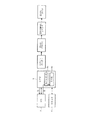
図1は、車両用ナビゲーション装置の全体構成を概略的に示している。車両用ナビゲーション装置(以下「カーナビ」という)1は、電源スイッチ2、リセットシーケンサ3(電源制御手段に相当)、電源4、CPU5(制御手段に相当)、DRAM6(バックアップ用記憶手段に相当)、SDカード7(記憶手段に相当)から構成されている。カーナビ1はバックアップ電源(以下「BU電源」という)8からの給電状態で動作する。BU電源8は、車両のイグニッションスイッチがオフされてメイン電源がオフしても給電状態が継続される電源であり、バッテリ電圧(例えば12V)を3.3Vに降圧して生成される。BU電源8には、電源スイッチ2、リセットシーケンサ3、電源4が接続されている。従って、カーナビ1をBU電源8に接続した状態では、BU電源8から電源スイッチ2、リセットシーケンサ3、電源4への給電状態となる。
Hereinafter, an embodiment of the present invention will be described with reference to the drawings.
FIG. 1 schematically shows the overall configuration of a vehicle navigation apparatus. A vehicle navigation device (hereinafter referred to as “car navigation”) 1 includes a
電源スイッチ2にSDカード7が接続されており、電源スイッチ2がオンした状態(動作状態)でBU電源8がSDカード7に接続される。電源4は、DC/DCコンバータ4a〜4cを内蔵しており、リセットシーケンサ3からの制御信号に応じて3.3V,1.1V,1.8Vを生成してCPU5へ出力する。リセットシーケンサ3にはタイマ3aとバックアップフラグ(以下「BUフラグ」という)3bが内蔵されており、BUフラグ3bは、リセットシーケンサ3が起動した状態でオフされている。リセットシーケンサ3は、後述するように車両のイグニッションスイッチから起動信号としてアクセサリオン信号(イグニッションスイッチがアクセサリ位置に位置した状態で例えばハイレベルとなるレベル信号)を受信するようになっており、その受信に応じて後述するように電源スイッチ2及び電源4を制御する。
The
SDカード7は、コントローラ7a、RAM7b及びNAND型フラッシュメモリ7cを内蔵して構成されている。コントローラ7aは、NAND型フラッシュメモリ7cの不良ブロックの管理、及び論理ブロックと物理ブロックとの対応関係をRAM7bに作成した変換テーブルで管理する。
即ち、NAND型フラッシュメモリ7cは、複数のメモリブロックに分割されており、そのメモリブロックが消去時の最小単位となる。NAND型フラッシュメモリ7cのブロックには製造時の不良である初期不良ブロックと、使用中に不良となった後発不良ブロックがあり、コントローラ7aは、それらの不良ブロックを使用しないようにブロックを管理している。また、NAND型フラッシュメモリ7cのデータ管理は、データ更新時は消去済み領域に更新データを書き込み、元のデータが存在する領域を消去するという、追加書き込み方式を採用していることから、ある論理ブロックに対応するデータが存在する物理ブロックは、固定ではなく、常にメモリ内を移動している。このため、コントローラ7aは、電源投入時に、全物理ブロックの論理ブロックアドレス情報格納領域をサーチし、RAM7b上に、論理ブロックと物理ブロックの変換テーブルを作成するようにしている。変換テーブル作成後は、この変換テーブルを参照すれば、論理ブロックに対応する物理ブロックを直ちに判断可能なため、全ブロックのサーチ動作は電源投入時に1回行われる。以後、コントローラ7aは、データの更新を行い、対応する物理ブロックの位置が変化した場合は、論理番地と物理番地の変換テーブルの更新作業を行い、次のアクセスに備える。
The
That is, the
SDカード7とCPU5との間は、データライン、アドレスライン、コマンドラインとで接続されており、それらのラインはSDカード7の仕様に基づいてプルアップ抵抗9を通じてCPU5の電源ラインである3.3Vラインと接続されている。SDカード7のNAND型フラッシュメモリ7cには、IPL(Initial Program Loader、ブートプログラムに相当)、OS(Operating System、「ブートプラグムの実行により読込まれるプログラム」に相当)、アプリケーションプログラム、地図データなどが記憶されている。IPLは、CPU5がOSを読み込むために必要とする最小限のプログラムである。
The
DRAM6は、CPU5によりデータが記憶されるもので、BU電源8に接続されたDC/DCコンバータ10から電源スイッチ11を通じて給電されおり、データの記憶状態が維持されている一方、後述するように異常発生時にはリセットシーケンサ3によりリセットされる。
The
さて、上述したようなSDカード7特有の事情により、電源投入時にコントローラ7aが行う初期設定処理に時間を要し、その間はCPU5がSDカード7にアクセスすることができない。この時間は、SDカード7のメーカ、仕様により異なるが、最大1秒見込む必要があることを確認している。つまり、CPU5は、SDカード7の電源投入時は、最大1秒間SDカード7にアクセスすることができないことから、その間はSDカード7からIPLを読込むことができず、車内LANを通じた要求に応じることができない。
Now, due to the circumstances peculiar to the
そこで、本実施の形態では、次のようにリセットシーケンサ3及びCPU5の動作を工夫した。
図2は、リセットシーケンサ3の動作を示すフローチャートである。カーナビ1をBU電源8に接続すると、リセットシーケンサ3に給電されて起動する。リセットシーケンサ3は、起動すると電源スイッチ2をオンするので(S1)、BU電源8がSDカード7に接続されて給電される。このBU電源8による給電状態は、バッテリが車両に接続されている限り継続することから、起動動作はカーナビ1をBU電源8に接続した状態での最初の1回のみである。但し、バッテリが完全に放電した後に充電されたり、バッテリが交換されたりした場合、或いはカーナビ1をBU電源8に再接続した場合には、リセットシーケンサ3が起動することから、最初の起動となる。
Therefore, in the present embodiment, the operations of the
FIG. 2 is a flowchart showing the operation of the
リセットシーケンサ3は、起動すると、スタンバイ状態となり、起動要因が発生するまで待機する(S2)。カーナビ1を取付けた作業者が確認のためにイグニッションスイッチをアクセサリオン位置に回すと(起動操作に相当)、起動信号としてアクセサリオン信号を受信するので(S2:ACC−ON)、電源4を動作させて1.1/1.8/3.3VをCPU5へ投入してから(S3)、CPU5をリセットする(S4)。
When the
CPU5は、リセットされることにより起動すると、起動処理を実行する。
図4は、CPU5の起動処理を示すフローチャートである。CPU5は、起動すると、リセットシーケンサ3のBUフラグ3bを読取り、BUフラグ3bがオンしているかを判定する。リセットシーケンサ3が起動した状態ではBUフラグ3bはオフしているので、待機処理を実行する。この待機処理とは、SDカード7が初期設定処理を実行するのに十分な時間待機するもので、例えば2秒が設定されている。待機処理終了後、BUフラグ3bをオンしてから、ブート処理を実行する。
When the
FIG. 4 is a flowchart showing the startup process of the
図5はCPU5のブート処理の手順を示している。CPU5のROM5aにはブートローダーとSDドライバが予め記憶されており、まず、ブートローダーを読取ってから、SDカード7にアクセス可能となるようにSDドライバを起動したり、SDカード7との通信を行うためのI/Fを設定したりした後、SDカード7にIPLを読出す読出しコマンドを送信する。この場合、上述したようにSDカード7の初期設定処理が終了していることから、IPLを読取ることができ、そのIPLを実行することによりOSを読取ることができる。
FIG. 5 shows a procedure for boot processing of the
図2に戻って、CPU5をリセットしたリセットシーケンサ3は、CPU5の起動が終了するのを待機し(S5)、タイムアウトした場合は(S5:タイムアウト)、異常であると判定してCPU5をリセットすることによりCPU5を再起動する(S6)。一方、CPU5の起動が終了した場合は(S5:終了)、動作状態に移行し、CPU5が正常に動作しているかを監視しながら(S7)、アクセサリオン信号の受信状態が継続しているかを判定する(S8)。CPU5が正常動作しない場合は(S7:NG)、CPU5をリセットする(S6)。
Returning to FIG. 2, the
図3は、リセットシーケンサ3によるCPU5のリセット動作を示している。CPU5は、起動後はタイマによる一定周期でウオッチドッグ用のクリア信号をリセットシーケンサ3に出力する。リセットシーケンサ3は、カウンタによるカウント動作を実行しており、規定時間内にCPU5からクリア信号を受信した場合はカウンタをクリアし、規定時間内にCPU5からクリア信号を受信しない場合はカウント値がFull(FFFF……)になると、異常であるとしてCPU5をリセットする。リセットの動作方式についてはこれに限らない。
FIG. 3 shows the reset operation of the
さて、リセットシーケンサ3は、動作状態でアクセサリがオフされた場合は(S8:OFF)、終了処理状態に移行する。終了処理状態に移行すると、処理終了タイマを起動し、CPU5に割り込みを掛けてデータをバックアップする(S9)。
図6及び図7は、データバックアップの手順を示すフローチャートであり、2つの手順がある。図6に示す第1の手順では、CPU5に割り込みを掛けると、CPU5は、キャッシュメモリとして機能するRAM5bに記憶されているデータをDRAM6へ書き込み、SDカード7へのバックデータがあるかを判定し、バックアップデータがある場合は、DRAM6の該当するバックアップデータをSDカード7へ転送する。DRAM6にバックアップを要するデータがある場合は、DRAM6をセルフリフレッシュする。このセルフリフレッシュとは、DRAM6に内蔵されたリフレッシュ回路で自動的にリフレッシュを行えるようにしたもので、一度リフレッシュの命令を与えれば、DRAM6に電力を供給するだけでデータ保持が可能になるため、電力消費を抑えることができる。
When the accessory is turned off in the operating state (S8: OFF), the
6 and 7 are flowcharts showing a data backup procedure, and there are two procedures. In the first procedure shown in FIG. 6, when the
一方、図7に示す第2の手順では、CPU5に割り込みを掛けると、CPU5は、RAM5bのデータをDRAM6に書込み、DRAM6にバックアップを要するデータがある場合は、DRAM6をセルフリフレッシュ状態とする。次に、SDカード7へのバックアップデータがある場合は、SDカード7へバックアップデータを書き込む。
以上のような手順により、CPU5のRAM5bに記憶されていたデータがバックアップされると共に、SDカード7にバックアップを要するデータが記憶される。
On the other hand, in the second procedure shown in FIG. 7, when the
Through the above procedure, the data stored in the
図2に戻って、リセットシーケンサ3は、終了処理状態で上述したようにデータをバックアップした後、正常に終了したかを判定し(S10)、タイマの時間内に正常に終了したときは(S10:OK)、タイマをクリアしてから、電源4を停止することによりCPU5を停止する(S12)。一方、タイマがタイムオーバとなった場合は(S10:NG)、異常が生じたとして、電源スイッチ2をオフすることにより強制終了すると同時にバックアップするメモリであるSDカード7またはDRAM6の電圧1.8Vまたは3.3Vをリセットする(S11)。これにより、CPU5及びDRAM6がリセットされるので、異常状態を解消して次の起動に備えることができる。
Returning to FIG. 2, the
ここで、SDカードとCPU5との間のラインであるデータライン、アドレスライン、コマンドラインは、プルアップする必要があるものの、プルアップ抵抗9をBU電源8に接続した場合、CPU5への停止状態であってもBU電源8からの電圧がCPU5に回り込んでCPU5が不安定となる虞がある。
しかしながら、本実施の形態では、プルアップ抵抗9をCPU5の電源ライン(3.3V)と接続するようにしたので、CPU5への給電が停止した状態ではプルアップ抵抗9の電圧は0Vとなり、CPU5に電圧が回り込んでしまうことを防止できる。
Here, the data line, the address line, and the command line, which are lines between the SD card and the
However, in this embodiment, since the pull-up
さて、車両が使用者に手渡され、使用者がアクセサリオン操作する場合は、2回目以降のアクセサリオン操作となる。この場合、SDカード7にはBU電源8からの給電状態が継続しており、リセットシーケンサ3のBUフラグ3bはオンしているので、図4の起動処理に示すように、リセットシーケンサ3により起動されたCPU5は、起動するにしても待機処理を実行することなくブート処理を実行してSDカード7からIPLを読取る。これにより、CPU5は、SDカード7からIPLを読取り、そのIPLの実行によりOSを読取るので、車内LANを通じた要求に確実に応えることができる。
Now, when the vehicle is handed to the user and the user performs an accessory-on operation, the accessory-on operation is performed for the second time and thereafter. In this case, since the power supply state from the
そして、リセットシーケンサ3は、上述したように起動時にタイマがタイムアップした場合は、CPU5をリセットし、CPU5の動作状態では、CPU5が正常に動作しているかを監視し、使用者によりアクセサリオフ操作された場合は(「起動操作の解除」に相当)、データのバックアップを実行し、正常に終了しない場合は、CPU5を強制終了すると同時にDRAMへの給電を停止する。
Then, as described above, the
このような実施の形態によれば、次のような効果を奏することができる。
リセットシーケンサ3は、BU電源8からの給電により起動した場合は、電源スイッチ2をオンすることによりSDカード7に給電し、アクセサリオン信号を受信した場合はCPU5に給電して起動し、起動したCPU5は、リセットシーケンサ3のBUフラグ3bがオフしていたときはSDカード7にアクセスするのを待機する待機処理を実行してからBUフラグ3bをオンすると共にSDカード7からIPLを読取るブート処理を実行し、BUフラグ3bがオンしていたときは待機処理を実行することなくブート処理を実行するので、BU電源8接続時にSDカード7が初期設定処理に時間を要するにしても、車両が使用者に手渡された状態では、アクセサリオン時にCPU5がIPLを直ちに読取り、そのIPLを実行することよりOSを読取って例えば外部からの指令に応じることができる。
According to such an embodiment, the following effects can be obtained.
When the
CPU5は、BU電源8に接続されたリセットシーケンサ3が保持するバックアップフラグのオンオフにより待機処理を実行するか否かを判定するので、CPU5への給電が停止するにしても、起動したCPU5は、バックアップフラグのオンオフにより最初の起動か否かを確実に判定することができる。
リセットシーケンサ3は、アクセサリオン信号が停止した場合はCPU5に割り込みを掛け、CPU5がデータをバックアップするようにしたので、CPU5のRAM5bに記憶されているバックアップが必要な地図データをSDカード7に記憶することができる。また、地図データをSDカード7に記憶することができない場合は、異常が生じたとして電源スイッチ2及び電源4を停止するので、異常状態を解除して初期状態とすることができる。
CPU5への給電が停止した状態では、SDカード7とCPU5とを接続する各ラインはプルアップ抵抗9を通じて0Vとなるので、プルアップ抵抗9をバックアップ電源8に接続する構成に比較して、バックアップ電源8からSDカード7とCPU5とを接続する各ラインの保護カードなどを介してCPU5に電圧が回り込んで不安定となってしまうことを防止できる。
Since the
When the accessory on signal stops, the
In the state where the power supply to the
(他の実施の形態)
本発明は、上記実施形態に限定されることなく、次のように変形または拡張できる。
CPU5は、電源4の起動時に初期設定処理なしにSDカード7が応答しない場合は最初の起動であると判断して初期化処理を実行し、起動時にSDカード7が応答した場合は2回目以降の起動であると判断して初期化処理を実行することなくブート処理を実行するようにしても良い。このような構成によれば、リセットシーケンサ3にバックアップ用フラグを設ける必要がないことから、リセットシーケンサ3の構成を簡単化することができる。
(Other embodiments)
The present invention is not limited to the above embodiment, and can be modified or expanded as follows.
When the
図面中、1は車両用ナビゲーション装置、2は電源スイッチ、3はリセットシーケンサ(電源制御手段)、4は電源、5はCPU(制御手段に相当)、6はDRAM(バックアップ用記憶手段)、7はSDカード(記憶手段)、7aはコントローラ、7cはNAND型フラッシュメモリ、8はバックアップ電源である。 In the drawings, 1 is a vehicle navigation device, 2 is a power switch, 3 is a reset sequencer (power control means), 4 is a power supply, 5 is a CPU (corresponding to control means), 6 is a DRAM (backup storage means), 7 Is an SD card (storage means), 7a is a controller, 7c is a NAND flash memory, and 8 is a backup power supply.
Claims (8)
車両に搭載されたバッテリの電圧を所定電圧に降圧してなるバックアップ電源と、
前記バックアップ電源と接続され、動作状態で前記記憶手段に前記バックアップ電源を接続する電源スイッチと、
前記バックアップ電源と接続され、動作状態で前記バックアップ電源から所定電圧を生成する電源と、
前記電源から給電されることにより起動した場合は前記記憶手段に前記バックアップ電源が接続された状態での最初の起動か否かを判定し、最初の起動であると判定した場合は、前記記憶手段による初期設定処理が終了するのを待機する待機処理を実行してから前記記憶手段からブートプラグムを読込むブート処理を実行し、2回目以降の起動であると判定した場合は、前記待機処理を実行することなく前記ブート処理を実行する制御手段と、
使用者による起動操作に応じて前記制御手段を起動するための起動信号を受信し、起動操作の解除により前記起動信号が停止するように設けられ、前記バックアップ電源と接続された場合は前記電源スイッチを動作し、起動信号が入力した場合は前記電源を動作し、前記起動信号が停止した場合は前記電源に対する動作状態を停止する電源制御手段と、
を備えたことを特徴とする車両用ナビゲーション装置。 At least the bootplum and the NAND flash memory storing the program read by the execution of this bootpragm, and all the defective blocks of the NAND flash memory are searched when the power is turned on, and the detected defective blocks are excluded. Storage means having a controller for executing an initial setting process for managing the correspondence between logical blocks and physical blocks;
A backup power source that lowers the voltage of the battery mounted on the vehicle to a predetermined voltage;
A power switch connected to the backup power source and connected to the storage means in the operating state;
A power source connected to the backup power source and generating a predetermined voltage from the backup power source in an operating state;
When the power supply is activated by being powered from the power supply, it is determined whether or not the backup power supply is connected to the storage means, and the storage means is determined to be the first activation. When the standby process for waiting for the completion of the initial setting process is executed, the boot process for reading the bootpragm from the storage means is executed, and when it is determined that the second and subsequent startups are performed, the standby process is performed. Control means for executing the boot process without executing
When receiving a start signal for starting the control means in response to a start operation by a user, the start signal is stopped by releasing the start operation, and when connected to the backup power source, the power switch Power control means for operating the power supply when a start signal is input, and stopping an operation state for the power supply when the start signal is stopped,
A vehicle navigation apparatus comprising:
前記制御手段は、起動時に前記バックアップフラグがオフしている場合は最初の起動であると判断すると共に前記バックアップフラグをオンし、起動時に前記バックアップフラグをオンしている場合は2回目以降の起動であると判断することを特徴とする請求項1記載の車両用ナビゲーション装置。 The power control means has a backup flag that is off when the backup power supply is connected;
When the backup flag is off at the time of startup, the control unit determines that the backup is the first startup and turns on the backup flag, and when the backup flag is on at the time of startup, the second and subsequent startups The vehicle navigation apparatus according to claim 1, wherein it is determined that
前記制御手段は、前記電源制御手段から終了処理が指令された場合は、自己に記憶しているバックアップが必要なデータを前記記憶手段に記憶するバックアップを実行することを特徴とする請求項1ないし3の何れかに記載の車両用ナビゲーション装置。 When the start signal is stopped, the power control means instructs the control means to end processing, and when the backup can be normally completed within a predetermined time, the power supply is stopped, and the power supply control means cannot be normally ended. If an abnormality occurs, stop the power switch and the power supply,
Wherein if the termination process from the power supply control means is instructed, the claims, characterized in execution to Rukoto backup for storing backup requires data stored in itself to the storage means The vehicle navigation device according to any one of 1 to 3.
前記制御手段は、前記電源制御手段から終了処理が指令された場合は、終了処理としてバックアップが必要なデータを前記バックアップ用記憶手段に記憶し、所定時間内にバックアップを正常に終了できなかった場合は異常が生じたとして前記バックアップ用記憶手段への給電を停止することを特徴とする請求項4記載の車両用ナビゲーション装置。 Powered by the backup power source, comprising backup storage means for storing backup data,
When the termination process is instructed from the power supply control unit, the control unit stores data that needs to be backed up as the termination process in the backup storage unit, and the backup cannot be completed normally within a predetermined time. 5. The vehicle navigation apparatus according to claim 4, wherein power supply to the backup storage means is stopped when an abnormality occurs.
Priority Applications (6)
| Application Number | Priority Date | Filing Date | Title |
|---|---|---|---|
| JP2010093945A JP5077385B2 (en) | 2010-04-15 | 2010-04-15 | Vehicle navigation device |
| CN201110090994.7A CN102248919B (en) | 2010-04-15 | 2011-04-12 | Navigation device for vehicle |
| US13/085,544 US9032195B2 (en) | 2010-04-15 | 2011-04-13 | Navigation device for vehicle |
| DE102011007240A DE102011007240A1 (en) | 2010-04-15 | 2011-04-13 | Car navigation device |
| TW100112965A TWI438402B (en) | 2010-04-15 | 2011-04-14 | Navigation device for vehicle |
| KR1020110035086A KR101219557B1 (en) | 2010-04-15 | 2011-04-15 | Navigation device for vehicle |
Applications Claiming Priority (1)
| Application Number | Priority Date | Filing Date | Title |
|---|---|---|---|
| JP2010093945A JP5077385B2 (en) | 2010-04-15 | 2010-04-15 | Vehicle navigation device |
Publications (2)
| Publication Number | Publication Date |
|---|---|
| JP2011227555A JP2011227555A (en) | 2011-11-10 |
| JP5077385B2 true JP5077385B2 (en) | 2012-11-21 |
Family
ID=44789097
Family Applications (1)
| Application Number | Title | Priority Date | Filing Date |
|---|---|---|---|
| JP2010093945A Expired - Fee Related JP5077385B2 (en) | 2010-04-15 | 2010-04-15 | Vehicle navigation device |
Country Status (6)
| Country | Link |
|---|---|
| US (1) | US9032195B2 (en) |
| JP (1) | JP5077385B2 (en) |
| KR (1) | KR101219557B1 (en) |
| CN (1) | CN102248919B (en) |
| DE (1) | DE102011007240A1 (en) |
| TW (1) | TWI438402B (en) |
Families Citing this family (4)
| Publication number | Priority date | Publication date | Assignee | Title |
|---|---|---|---|---|
| JP5382084B2 (en) * | 2011-10-07 | 2014-01-08 | 株式会社デンソー | Vehicle equipment |
| KR101334310B1 (en) * | 2011-12-07 | 2013-11-28 | 콘티넨탈 오토모티브 일렉트로닉스 유한회사 | Apparatus for controlling a booting of cluster for vehicle |
| WO2014038115A1 (en) * | 2012-09-06 | 2014-03-13 | パナソニック株式会社 | Semiconductor integrated circuit |
| TW201826136A (en) * | 2017-01-13 | 2018-07-16 | 致伸科技股份有限公司 | Bluetooth pairing system and method for operating a bluetooth pairing system |
Family Cites Families (28)
| Publication number | Priority date | Publication date | Assignee | Title |
|---|---|---|---|---|
| JP3776493B2 (en) | 1995-12-27 | 2006-05-17 | オリンパス株式会社 | Image recording device |
| JP3500919B2 (en) | 1997-07-30 | 2004-02-23 | 株式会社デンソー | Vehicle navigation system |
| JP4079506B2 (en) | 1997-08-08 | 2008-04-23 | 株式会社東芝 | Method for controlling nonvolatile semiconductor memory system |
| US6496946B2 (en) * | 1999-05-10 | 2002-12-17 | Motorola, Inc. | Electronic control apparatus with memory validation and method |
| US7690031B2 (en) | 2000-01-06 | 2010-03-30 | Super Talent Electronics, Inc. | Managing bad blocks in flash memory for electronic data flash card |
| JP2002163128A (en) * | 2000-11-29 | 2002-06-07 | Fujitsu Ten Ltd | Computer device |
| US7107480B1 (en) * | 2000-12-22 | 2006-09-12 | Simpletech, Inc. | System and method for preventing data corruption in solid-state memory devices after a power failure |
| JP4655398B2 (en) | 2001-03-29 | 2011-03-23 | 株式会社デンソー | Vehicle control device with backup function |
| CN1302390C (en) * | 2002-07-25 | 2007-02-28 | 联想(北京)有限公司 | Method and apparatus for using NOT-AND flash as system memory |
| JP2004118336A (en) * | 2002-09-24 | 2004-04-15 | Clarion Co Ltd | Access protecting device |
| CN1295602C (en) * | 2003-04-23 | 2007-01-17 | 华为技术有限公司 | System of capable of identifying cold boot and warm boot, and method for quickenning speed of starting up system |
| JP2004341817A (en) * | 2003-05-15 | 2004-12-02 | Matsushita Electric Ind Co Ltd | Information processing method and program, and navigation system |
| KR100678047B1 (en) * | 2004-05-06 | 2007-02-02 | 삼성전자주식회사 | Mobile communication terminal having nand flash memory and booting method thereof |
| KR101115149B1 (en) * | 2005-02-21 | 2012-02-24 | 주식회사 현대오토넷 | Apparatus for a fast booting and managing power in a car system with a plurality of peripherals |
| US7352621B2 (en) * | 2005-06-23 | 2008-04-01 | Intel Corporation | Method for enhanced block management |
| US7711923B2 (en) * | 2006-06-23 | 2010-05-04 | Microsoft Corporation | Persistent flash memory mapping table |
| CN101118783A (en) * | 2006-09-07 | 2008-02-06 | 晶天电子(深圳)有限公司 | Electronic data flash memory fasten with flash memory bad blocks control system |
| CN101105752A (en) * | 2006-10-26 | 2008-01-16 | 福昭科技(深圳)有限公司 | Processing method for embedded type system using NAND flash memory storage and start-up |
| JP4937066B2 (en) * | 2006-11-02 | 2012-05-23 | 日立オートモティブシステムズ株式会社 | Electronic control device |
| CN100524217C (en) * | 2007-01-04 | 2009-08-05 | 炬力集成电路设计有限公司 | Embedded system guiding method and device |
| US8527691B2 (en) * | 2007-07-31 | 2013-09-03 | Panasonic Corporation | Nonvolatile memory device and nonvolatile memory system with fast boot capability |
| JP2009098726A (en) * | 2007-10-12 | 2009-05-07 | Bosch Corp | Initialization method for stored data |
| KR20090042039A (en) * | 2007-10-25 | 2009-04-29 | 삼성전자주식회사 | Data management method for nonvolatile memory device |
| US7979626B2 (en) * | 2008-05-13 | 2011-07-12 | Microsoft Corporation | Flash recovery employing transaction log |
| JP2009282566A (en) * | 2008-05-19 | 2009-12-03 | Fujitsu Ten Ltd | Electronic control device |
| CN101520735B (en) * | 2008-12-18 | 2013-09-18 | 康佳集团股份有限公司 | Method for starting guidance program in flash memory, network television and set-top box thereof |
| JP2010211734A (en) * | 2009-03-12 | 2010-09-24 | Toshiba Storage Device Corp | Storage device using nonvolatile memory |
| GB2472050B (en) * | 2009-07-22 | 2013-06-19 | Wolfson Microelectronics Plc | Power management apparatus and methods |
-
2010
- 2010-04-15 JP JP2010093945A patent/JP5077385B2/en not_active Expired - Fee Related
-
2011
- 2011-04-12 CN CN201110090994.7A patent/CN102248919B/en not_active Expired - Fee Related
- 2011-04-13 US US13/085,544 patent/US9032195B2/en not_active Expired - Fee Related
- 2011-04-13 DE DE102011007240A patent/DE102011007240A1/en not_active Withdrawn
- 2011-04-14 TW TW100112965A patent/TWI438402B/en not_active IP Right Cessation
- 2011-04-15 KR KR1020110035086A patent/KR101219557B1/en active IP Right Grant
Also Published As
| Publication number | Publication date |
|---|---|
| TWI438402B (en) | 2014-05-21 |
| TW201207358A (en) | 2012-02-16 |
| CN102248919A (en) | 2011-11-23 |
| DE102011007240A8 (en) | 2012-02-16 |
| US9032195B2 (en) | 2015-05-12 |
| US20110258427A1 (en) | 2011-10-20 |
| KR20110115549A (en) | 2011-10-21 |
| JP2011227555A (en) | 2011-11-10 |
| KR101219557B1 (en) | 2013-01-09 |
| DE102011007240A1 (en) | 2011-11-10 |
| CN102248919B (en) | 2014-12-10 |
Similar Documents
| Publication | Publication Date | Title |
|---|---|---|
| JP5382084B2 (en) | Vehicle equipment | |
| JP5402693B2 (en) | Disk array device control method and disk array device | |
| US10754558B2 (en) | Vehicular device | |
| CN104850435B (en) | Power source management controller and method | |
| US6438708B1 (en) | Information processing apparatus that can hold internal information | |
| JPH1097353A (en) | Computer system and resume processing method applied to the same system | |
| JP2004038529A (en) | Information processor | |
| JP5077385B2 (en) | Vehicle navigation device | |
| JP2007334403A (en) | System and method for supporting trouble of computer system | |
| KR101115149B1 (en) | Apparatus for a fast booting and managing power in a car system with a plurality of peripherals | |
| WO2012172708A1 (en) | Backup device and operating method for backup device | |
| WO2022028350A1 (en) | Electronic device and method for controlling update of data in electronic device | |
| JP6408450B2 (en) | Electronic control unit for automobile | |
| JP6252799B2 (en) | Arithmetic processing device and control method thereof | |
| CN113918001B (en) | Embedded network equipment system upgrading data protection device and method | |
| JP2017072920A (en) | Information processing device | |
| JP2740685B2 (en) | Storage device backup circuit | |
| JP5176731B2 (en) | Access device | |
| JP2001056226A (en) | Navigation system | |
| JPH06124148A (en) | Computer having suspend/resume function | |
| JP2013196112A (en) | Memory system and method for controlling power saving of the same | |
| JP2021060747A (en) | Microcomputer | |
| JPS63298654A (en) | Microcomputer | |
| JP2011145891A (en) | Information processing device |
Legal Events
| Date | Code | Title | Description |
|---|---|---|---|
| A621 | Written request for application examination |
Free format text: JAPANESE INTERMEDIATE CODE: A621 Effective date: 20120321 |
|
| A131 | Notification of reasons for refusal |
Free format text: JAPANESE INTERMEDIATE CODE: A131 Effective date: 20120508 |
|
| A521 | Request for written amendment filed |
Free format text: JAPANESE INTERMEDIATE CODE: A523 Effective date: 20120704 |
|
| A521 | Request for written amendment filed |
Free format text: JAPANESE INTERMEDIATE CODE: A523 Effective date: 20120705 |
|
| TRDD | Decision of grant or rejection written | ||
| A01 | Written decision to grant a patent or to grant a registration (utility model) |
Free format text: JAPANESE INTERMEDIATE CODE: A01 Effective date: 20120731 |
|
| A01 | Written decision to grant a patent or to grant a registration (utility model) |
Free format text: JAPANESE INTERMEDIATE CODE: A01 |
|
| A61 | First payment of annual fees (during grant procedure) |
Free format text: JAPANESE INTERMEDIATE CODE: A61 Effective date: 20120813 |
|
| FPAY | Renewal fee payment (event date is renewal date of database) |
Free format text: PAYMENT UNTIL: 20150907 Year of fee payment: 3 |
|
| R151 | Written notification of patent or utility model registration |
Ref document number: 5077385 Country of ref document: JP Free format text: JAPANESE INTERMEDIATE CODE: R151 |
|
| FPAY | Renewal fee payment (event date is renewal date of database) |
Free format text: PAYMENT UNTIL: 20150907 Year of fee payment: 3 |
|
| R250 | Receipt of annual fees |
Free format text: JAPANESE INTERMEDIATE CODE: R250 |
|
| R250 | Receipt of annual fees |
Free format text: JAPANESE INTERMEDIATE CODE: R250 |
|
| R250 | Receipt of annual fees |
Free format text: JAPANESE INTERMEDIATE CODE: R250 |
|
| R250 | Receipt of annual fees |
Free format text: JAPANESE INTERMEDIATE CODE: R250 |
|
| R250 | Receipt of annual fees |
Free format text: JAPANESE INTERMEDIATE CODE: R250 |
|
| LAPS | Cancellation because of no payment of annual fees |