JP5069825B2 - Optical fiber compensation for dispersion, gain tilt, and band-pumping nonlinearity - Google Patents
Optical fiber compensation for dispersion, gain tilt, and band-pumping nonlinearity Download PDFInfo
- Publication number
- JP5069825B2 JP5069825B2 JP2000555336A JP2000555336A JP5069825B2 JP 5069825 B2 JP5069825 B2 JP 5069825B2 JP 2000555336 A JP2000555336 A JP 2000555336A JP 2000555336 A JP2000555336 A JP 2000555336A JP 5069825 B2 JP5069825 B2 JP 5069825B2
- Authority
- JP
- Japan
- Prior art keywords
- pumping
- raman
- fiber
- gain
- dispersion
- Prior art date
- Legal status (The legal status is an assumption and is not a legal conclusion. Google has not performed a legal analysis and makes no representation as to the accuracy of the status listed.)
- Expired - Lifetime
Links
Images


Classifications
-
- H—ELECTRICITY
- H01—ELECTRIC ELEMENTS
- H01S—DEVICES USING THE PROCESS OF LIGHT AMPLIFICATION BY STIMULATED EMISSION OF RADIATION [LASER] TO AMPLIFY OR GENERATE LIGHT; DEVICES USING STIMULATED EMISSION OF ELECTROMAGNETIC RADIATION IN WAVE RANGES OTHER THAN OPTICAL
- H01S3/00—Lasers, i.e. devices using stimulated emission of electromagnetic radiation in the infrared, visible or ultraviolet wave range
- H01S3/05—Construction or shape of optical resonators; Accommodation of active medium therein; Shape of active medium
- H01S3/06—Construction or shape of active medium
- H01S3/063—Waveguide lasers, i.e. whereby the dimensions of the waveguide are of the order of the light wavelength
- H01S3/067—Fibre lasers
-
- H—ELECTRICITY
- H01—ELECTRIC ELEMENTS
- H01S—DEVICES USING THE PROCESS OF LIGHT AMPLIFICATION BY STIMULATED EMISSION OF RADIATION [LASER] TO AMPLIFY OR GENERATE LIGHT; DEVICES USING STIMULATED EMISSION OF ELECTROMAGNETIC RADIATION IN WAVE RANGES OTHER THAN OPTICAL
- H01S3/00—Lasers, i.e. devices using stimulated emission of electromagnetic radiation in the infrared, visible or ultraviolet wave range
- H01S3/30—Lasers, i.e. devices using stimulated emission of electromagnetic radiation in the infrared, visible or ultraviolet wave range using scattering effects, e.g. stimulated Brillouin or Raman effects
- H01S3/302—Lasers, i.e. devices using stimulated emission of electromagnetic radiation in the infrared, visible or ultraviolet wave range using scattering effects, e.g. stimulated Brillouin or Raman effects in an optical fibre
-
- H—ELECTRICITY
- H04—ELECTRIC COMMUNICATION TECHNIQUE
- H04B—TRANSMISSION
- H04B10/00—Transmission systems employing electromagnetic waves other than radio-waves, e.g. infrared, visible or ultraviolet light, or employing corpuscular radiation, e.g. quantum communication
- H04B10/25—Arrangements specific to fibre transmission
- H04B10/2507—Arrangements specific to fibre transmission for the reduction or elimination of distortion or dispersion
- H04B10/2513—Arrangements specific to fibre transmission for the reduction or elimination of distortion or dispersion due to chromatic dispersion
- H04B10/2525—Arrangements specific to fibre transmission for the reduction or elimination of distortion or dispersion due to chromatic dispersion using dispersion-compensating fibres
- H04B10/25253—Arrangements specific to fibre transmission for the reduction or elimination of distortion or dispersion due to chromatic dispersion using dispersion-compensating fibres with dispersion management, i.e. using a combination of different kind of fibres in the transmission system
-
- H—ELECTRICITY
- H04—ELECTRIC COMMUNICATION TECHNIQUE
- H04B—TRANSMISSION
- H04B10/00—Transmission systems employing electromagnetic waves other than radio-waves, e.g. infrared, visible or ultraviolet light, or employing corpuscular radiation, e.g. quantum communication
- H04B10/29—Repeaters
- H04B10/291—Repeaters in which processing or amplification is carried out without conversion of the main signal from optical form
- H04B10/2912—Repeaters in which processing or amplification is carried out without conversion of the main signal from optical form characterised by the medium used for amplification or processing
- H04B10/2916—Repeaters in which processing or amplification is carried out without conversion of the main signal from optical form characterised by the medium used for amplification or processing using Raman or Brillouin amplifiers
-
- H—ELECTRICITY
- H01—ELECTRIC ELEMENTS
- H01S—DEVICES USING THE PROCESS OF LIGHT AMPLIFICATION BY STIMULATED EMISSION OF RADIATION [LASER] TO AMPLIFY OR GENERATE LIGHT; DEVICES USING STIMULATED EMISSION OF ELECTROMAGNETIC RADIATION IN WAVE RANGES OTHER THAN OPTICAL
- H01S3/00—Lasers, i.e. devices using stimulated emission of electromagnetic radiation in the infrared, visible or ultraviolet wave range
- H01S3/05—Construction or shape of optical resonators; Accommodation of active medium therein; Shape of active medium
- H01S3/06—Construction or shape of active medium
- H01S3/063—Waveguide lasers, i.e. whereby the dimensions of the waveguide are of the order of the light wavelength
- H01S3/067—Fibre lasers
- H01S3/06754—Fibre amplifiers
- H01S3/06758—Tandem amplifiers
-
- H—ELECTRICITY
- H01—ELECTRIC ELEMENTS
- H01S—DEVICES USING THE PROCESS OF LIGHT AMPLIFICATION BY STIMULATED EMISSION OF RADIATION [LASER] TO AMPLIFY OR GENERATE LIGHT; DEVICES USING STIMULATED EMISSION OF ELECTROMAGNETIC RADIATION IN WAVE RANGES OTHER THAN OPTICAL
- H01S3/00—Lasers, i.e. devices using stimulated emission of electromagnetic radiation in the infrared, visible or ultraviolet wave range
- H01S3/09—Processes or apparatus for excitation, e.g. pumping
- H01S3/091—Processes or apparatus for excitation, e.g. pumping using optical pumping
- H01S3/094—Processes or apparatus for excitation, e.g. pumping using optical pumping by coherent light
- H01S3/094003—Processes or apparatus for excitation, e.g. pumping using optical pumping by coherent light the pumped medium being a fibre
- H01S3/094015—Processes or apparatus for excitation, e.g. pumping using optical pumping by coherent light the pumped medium being a fibre with pump light recycling, i.e. with reinjection of the unused pump light back into the fiber, e.g. by reflectors or circulators
-
- H—ELECTRICITY
- H04—ELECTRIC COMMUNICATION TECHNIQUE
- H04B—TRANSMISSION
- H04B2210/00—Indexing scheme relating to optical transmission systems
- H04B2210/003—Devices including multiple stages, e.g., multi-stage optical amplifiers or dispersion compensators
Landscapes
- Physics & Mathematics (AREA)
- Electromagnetism (AREA)
- Engineering & Computer Science (AREA)
- Plasma & Fusion (AREA)
- Optics & Photonics (AREA)
- Computer Networks & Wireless Communication (AREA)
- Signal Processing (AREA)
- Optical Modulation, Optical Deflection, Nonlinear Optics, Optical Demodulation, Optical Logic Elements (AREA)
- Optical Communication System (AREA)
- Glass Compositions (AREA)
Abstract
Description
【0001】
(技術分野)
本発明は一般的には、電気通信、ケーブル・テレビ(cable television)及び他のファイバ光学アプリケーションのためのファイバ光学において使用される光学増幅器に関連する。より特定的には、本発明は、利得傾斜を最小化するための方法及び帯域ポンピングの間の非線形相互作用を最小化するための装置と同様に、ファイバ光学リンクに対する分散補償も供給する光学増幅器に関連する。
【0002】
(背景技術)
帯域幅に対する要求は、データ通信及びインターネット等のアプリケーションにより、ファイバ光学スーパーハイウェイ(fiber-optic superhighway)で急激に増加し続けている。その結果、各チャネルに対してより速い速度−いわゆる時分割多重伝送システム−及び複数の波長の光−いわゆる波長分割多重伝送(wavelength-division multiplexing)(WDM)を使用することによって、光学ファイバの帯域幅を活用することに多くの努力が費やされる。
【0003】
現在使用されているファイバ光学ネットワークのほとんどは、2種類のファイバ:スタンダード単一モード・ファイバ(standard single-mode fiber)(「スタンダード」ファイバ)又は分散シフト・ファイバ(dispersion-shifted fiber)(DSF)のうち一つを使用する。スタンダード・ファイバは、およそ1310ナノメートルのゼロ分散波長を有し、及び前記分散は主に前記固有のガラス分散から生じる。アメリカ合衆国及び世界のほとんどにおける地上ネットワークのほとんどは、実際には、スタンダード・ファイバに基づく。一方で、DSFにおいては、前記ゼロ分散波長をより長い波長にシフトする(shift)ために、導波路分散が使用される。従来のDSFは、石英ファイバ(fused silica fiber)における最小限の損失と同時に、1550ナノメートルでのゼロ分散波長を有するであろう。しかしながら、前記ゼロ分散波長は、追加される導波路分散の量を変化させることによって、シフトされることができる。DSFは、新しい長距離リンクにおけるのと同様に、日本及びイタリアの2カ国だけで使用される。
【0004】
ファイバ光学伝送線に対する制約要素は、損失、分散及び利得等化を含む。損失は、内在的拡散、吸収及び欠損等の他の外在的効果によって、信号がファイバにおいて通過すると減弱するという事実を意味する。例えば光学増幅器は、前記損失を補償するために使用されることができる。分散とは、異なる周波数の光が異なる速度で移動することを意味し、及びそれは物質的な特性並びに導波効果の両方に起因する。多重波長システムを使用する時、及び周波数と利得の非均一性によって、利得等化は、異なる波長チャネルに亘って前記利得を安定化することを要求される。
【0005】
これらの制約を克服するための典型的な解決法は、これらの問題の各々を補償するために、伝送システム素子に周期的に置かれることである。例えば、図1は、分散コンペンセータ(dispersion compensator)40が前記分散を補償するために使用されることができ、光学増幅器50は前記損失を相殺させるために使用されることができ、及び利得等化素子60は、前記利得を均すために使用されることができることを示す。分散コンペンセータの例は、チャープ・ファイバ回折格子及び分散補償ファイバ(dispersion compensating fiber)(DCF)を含む。光学増幅器の例は、エルビウムドープファイバ増幅器(erbium-doped fiber amplifier)(EDFA)、ラマン増幅器、及び非線形ファイバ増幅器(non-linear fiber amplifier)(NLFA)を含む。アメリカ合衆国特許第5,778,014号は、サニャック・ラマン増幅器及びカスケード・レーザ(cascade laser)を開示する。
【0006】
最後に、利得イコライザ(gain equalizer)は、マッハ・ツェンダ干渉計及び長期回折格子を含む。これら個別の構成要素からシステムを構築するよりも、図1に記載の機能の二つ以上を、アメリカ合衆国特許第5,887,093号に記載の単一の構成要素へと結合させる方が簡単であり、より費用効果的であるかもしれない。
【0007】
WDMシステムにおいて生じる他の問題は、前記ファイバにおける非線形性を通したチャネルの間の相互作用及びクロストーク(crosstalk)である。特に、四波混合(four-wave mixing)(4WM)は、異なる波長チャネルの間のエネルギ交換を生じさせるが、4WMのみが、ほぼゼロ分散波長で位相整合する。その結果、ファイバ・リンクが従来のDSFから作られる場合、およそ1540乃至1560ナノメートルからWDMシステムを操作することは困難である。典型的なEDFAは、1535乃至1565ナノメートルの利得を有するので、これは大変に残念なことであることがわかり、及びより均一な利得帯域は、およそ1540乃至1560ナノメートルである。問題となりうる第二のファイバ非線形性は、変調不安定性(modulation instability)(MI)であり、それは前記ファイバの非線形屈折率が位相整合に役立つ4WMである。しかしながら、前記分散が正であり又はいわゆるソリトン状況(soliton regime)である時、MIのみが位相整合する。それゆえに、MIはゼロ分散波長よりも短い波長で動作することによって避けられることができる。
【0008】
個別のファイバに対する帯域幅利用が増加するにつれて、伝送に使用される帯域の数が増加する。多くの帯域を使用するWDMシステムに対して、多重帯域シナリオ(multi-band scenario)における増幅の間の相互作用によってさらなる複雑性が生じる。特に、特定のシステム設計が、多重帯域伝送システムにおけるラマン増幅に必要となる。第一に、新しい非線形性ペナルティが、チャネル間のラマン効果からの利得傾斜から生じる。これは、長波長チャネルが、短波長チャネルからエネルギを奪う傾向にあるので、生じる。それゆえに、新しいWDMチャネルの追加を伴う、現存チャネル上の利得傾斜を最小化するための手段が必要とされる。
【0009】
4WM及びラマン利得傾斜の両方の効果を最小化するために、他の技術手段は分布ラマン増幅を使用するであろう。多重帯域を有するWDMシステムにおいて、前記伝送線に沿った、異なるポンピングの間の相互作用から、複雑性が生じる。
【0010】
アメリカ合衆国特許第5,883,736号は、ER添加光学ファイバ増幅器を開示する。
【0011】
アメリカ合衆国特許第5,673,280号は、低ノイズ光学ファイバ・ラマン増幅器を具備する物品を開示する。
【0012】
アメリカ合衆国特許第5,623,508号は、逆ポンピング光学ファイバ・ラマン増幅器を具備する物品を開示する。
【0013】
(発明の開示)
本発明の目的は、前記増幅器の利得ファイバが同時に前記分散補償を実行するラマン増幅器等、単一の光学素子を通して、分散補償と光学増幅器機能を結合させることである。
本発明の他の目的は、前記ファイバ光学リンクがスタンダードか、又はDSファイバを使用するかによって、前記ラマン増幅器の異なる設計を供給することである。
本発明のさらに他の目的は、WDMシステムが、DSファイバ・リンクを介して、分散補償ファイバを有するラマン増幅器における「紫色」帯域を使用することによって、4WM及びMIからの非線形性の制約を避けることができるようにすることである。
【0014】
本発明のさらに他の目的は、現存する帯域の下及び上の帯域の対称的追加によって、現存する従来の帯域への利得傾斜の効果を最小化することである。前記より長い波長チャネルが、エルビウムドープファイバ増幅器で増幅される一方で、前記より短い波長システムは、ディスクリート又は分布ラマン増幅器で有利に増幅されてもよい。
【0015】
最後に、本発明のさらに他の目的は、分布ラマン増幅を使用することによって、高密度WDMシステムにおけるファイバ非線形効果を避けることである。多重帯域システムにおけるポンピングの間の相互作用を避けるために、ラマン利得を通したポンピングの間の相互作用を最小化するために、隣接する帯域ポンピングを直交させるための手段が説明される。それゆえに、異なる帯域に対するポンピングの間の相互作用を低減させるために、それらが空間的、方向的又は極性的に直交又は非重複になるように、異なる帯域に対するポンピングを多重送信する手段が供給される。
【0016】
長さ、光学損失、分散、分散の符号、及び遮断波長を有する少なくとも一つの伝送リンクを含むファイバ光学伝送システムにおける、本発明の上述の目的及び他の目的を実行するにあたり、本発明は、分散を補償するため及び前記光学損失を相殺させるための単一光学素子を含む。前記光学素子は、信号波長を有する光学信号を受信するための入力ポートと、光学損失を有し並びに前記光学信号を増幅するための入力ポートに接続された分布利得媒体と、及び前記光学信号が、前記伝送リンク並びに前記利得媒体の光学損失を補償するための有効利得を受けるのに十分に高いポンピングレベルで、前記分布利得媒体をポンピングするためのポンピング光を生成するためのポンピング波長を有するポンピング機構を含む。前記光学素子はさらに、前記増幅された光学信号を出力するための出力ポートを含む。
【0017】
前記分布利得媒体は、典型的には長さ、分散及び分散の符号を有する利得ファイバである。前記利得ファイバは、実質的な大きさにおいて、反対の符号のものを除く、前記少なくとも一つの伝送リンクの分散−長さ積と等しい分散−長さ積を有する。また、前記利得ファイバが、前記ポンピング波長及び前記信号波長の両方に対する単一空間モードになるように、前記利得ファイバは、前記ポンピング波長より短い遮断波長を有する。
【0018】
前記光学信号は、開ループで増幅されてもよい。
【0019】
前記ポンピング機構は、少なくとも一つのレーザ・ダイオード、ラマン・オシレータ、又はラマン波長シフタでもよい。
【0020】
一つの実施形態において、前記利得ファイバは、前記ポンピング機構によって双方向にポンピングされる。
【0021】
他の実施形態において、前記利得ファイバは、二つの個別の区分を有し、及び前記ポンピング機構は、逆伝播で前記二つの区分をポンピングする。
本発明はさらに、アイソレータ、利得等化素子及び/又は前記二つの区分を接続するための光学アド/ドロップ・マルチプレクサを含む。
【0022】
さらに他の実施形態において、ポンピング分岐は、前記ポンピング機構を分岐させるために前記入力及び出力ポートに結合され、前記利得ファイバは、前記入力及びに出力ポートによって分割された個別の第一及び第二の区分を有し、及び前記ポンピング機構は、逆伝播で前記第一の区分をポンピングし並びに前記ポンピング機構の力を使い果たすまで前記第二の区分をポンピングする。
【0023】
前記光学信号は、閉ループでも増幅されてよい。
【0024】
前記利得ファイバは、前記ポンピング機構によって双方向にポンピングされる広帯域キャビティを少なくとも部分的に画定してもよい。この場合、前記利得ファイバは、ラマン利得ファイバでもよく、及び前記広帯域キャビティは、サニャック・ラマン・キャビティでもよい。
【0025】
他の実施形態において、前記分布利得媒体は、チャープ・ブラグ回折格子を有する循環ループ・キャビティを含み、及び前記利得ファイバは、前記ポンピング機構によって逆伝播でポンピングされる二つの個別の区分を有する。
【0026】
前記伝送線が、異なる波長チャネルに亘って非均一の利得を有する多重波長伝送線である時、前記異なる波長チャネルに亘る非均一の利得を均一にするための、第二の光学素子が供給されてもよい。前記第二の光学素子は、マッハ・ツェンダ干渉計の少なくとも一つの段を含む。前記分布利得機構は、二つの個別の区分を有する利得ファイバでもよく、及び前記第二の光学素子は、前記二つの区分を接続する。
【0027】
前記少なくとも一つの伝送リンクが、少なくとも一つのファイバ非線形性効果及びゼロ分散波長を有するDSFを含む、1430乃至1530ナノメートルの紫色帯域で動作する伝送システムにおいて、前記単一光学素子は、前記少なくとも一つのリンクにおいて、前記少なくとも一つのファイバ非線形性効果を避けるために、前記ゼロ分散波長から十分に離れた紫色帯域において、利得を供給する。前記利得ファイバは、スタンダード分散ファイバでもよい。
【0028】
前記少なくとも一つのファイバ非線形性は、四波混合及び/又は変調不安定性でもよい。
【0029】
前記少なくとも一つの伝送リンクは、異なる波長チャネルに亘る非均一利得を有してもよく、及び本発明はさらに、前記異なる波長チャネルに亘る前記非均一利得を均一にするための前記単一光学素子に接続された第二の光学素子を含む。前記第二の光学素子は、マッハ・ツェンダ干渉計の少なくとも一つの段を含んでもよい。
【0030】
前記利得ファイバは、集積分散が、実質的に紫色帯域の真中に相殺されるように選択された分散補償ファイバでもよい。
【0031】
さらに、本発明の上述の目的及び他の目的を実行するにあたり、多重波長伝送線を含むファイバ光学多重帯域システムにおいて、波長の追加の帯域が追加される時に、波長の少なくとも一つの現存する帯域内で利得傾斜を最小化させるための方法が、供給される。前記方法は、前記波長の少なくとも一つの現存する帯域におけるエネルギ変化を最小化するために、より短い及びより長い波長帯域を得るために前記波長の少なくとも一つの現存する帯域の上及び下の両方に実質的に等しい数の追加帯域を追加することを含む。前記方法はまた、前記より短い及びより長い波長帯域の各々が利得を有するように、前記より短い及びより長い波長帯域を増幅することも含む。
【0032】
前記より短い波長帯域を増幅する段階は、ディスクリート又は分布ラマン増幅器のいずれかで達成されてもよい。
【0033】
前記より長い波長帯域を増幅する段階は、エルビウムドープファイバ増幅器で達成されてもよい。前記より短い波長帯域の少なくとも一つにおける利得は、前記より長い波長帯域の少なくとも一つにおける利得よりも大きい。
【0034】
前記より短い波長帯域を増幅する段階は、分布の形態でなされてもよい。
【0035】
さらに、多重波伝送線を含むファイバ光学多重帯域伝送システムにおける本発明の上述の目的及び他の目的を実行するにあたり、一つの装置が供給される。前記装置は、増幅を得るための前記伝送線の異なる帯域をポンピングするための複数の帯域ポンピングを含み、異なる帯域に対する帯域ポンピングは、エネルギを交換することによって非線形に相互作用する。前記装置は、前記非線形相互作用を最小化するために、隣接する帯域ポンピングを直交させるための手段も含む。
【0036】
前記増幅は分布ラマン増幅でもよく、及び前記エネルギはラマン・エネルギである。
【0037】
交互の帯域ポンピングは、前記異なる帯域に対する帯域ポンピングの間の相互作用を最小化にするために、空間的に分散されてもよい。
【0038】
交互の帯域ポンピングは、前記異なる帯域に対する帯域ポンピングの間の相互作用を最小化するために、交差偏光されてもよい。
前記複数の帯域ポンピングは、分布ラマン増幅器の純粋分布システムを画定してもよい。
【0039】
代替的には、前記複数の帯域ポンピングは、ディスクリート及び分布増幅器の複合システムを画定してもよい。
【0040】
前記複数の帯域ポンピングは、ディスクリート・レーザ・ダイオード又は前記伝送線をポンピングするためのラマン・オシレータを含んでもよい。
【0041】
本発明に従って、分散管理ラマン増幅器(Dispersion Managing Raman Amplifier)(DMRA)は、これも分散コンペンセータとして機能する利得ファイバを使用して実行される。前記遮断波長が、前記ポンピング波長よりも短くなるように、前記ファイバは、前記ポンピング及び信号波長の両方に対して単一モード(single mode)であるべきである。前記ファイバの長さ及び分散は、理想的には伝送リンクと同じ大きさの分散−長さ積を有するが、分散の反対の符号を有するように選択されるべきである。前記ポンピングレベルは、前記分散補償ファイバ及び前記伝送リンクからの損失の合計よりも大きい利得を供給するように選択されるべきである。また、前記ポンピング体系は、前記ポンピング光に対して
3デシベル損失長内にとどまるように選択されるべきである。
一つの実施形態において、大きな負の分散(例;D<−80毎秒/ナノメートル−キロメートル)を有する分散補償ファイバ(dispersion-compensating fiber)(DCF)が、スタンダード・ファイバを使用してリンクの分散を補償するために使用される。前記ファイバ・リンクが45キロメートルの長さである場合、前記DCFは、1500ナノメートルでの分散補償に対して約7.8キロメートルの長さであるべきである。また、前記利得は、14.2デシベルを超え、及び前記利得ファイバは、双方向か又は二つの区分においてポンピングされる必要があるかもしれない。
【0042】
他の実施形態において、スタンダード・ファイバは、従来のDSファイバを使用し、及び「紫色帯域」において動作することで、リンクの分散を補償するために使用される。前記ファイバ・リンクが45キロメートルの長さである場合、前記スタンダード利得ファイバは、1500ナノメートルにおける分散補償に対して約13.3キロメートルの長さであるべきである。また、前記利得は14.2デシベルを超えるべきであり、前記利得ファイバは、双方向に又は二つの区分において、ポンピングされる必要があるかもしれない。
【0043】
前記利得ファイバが、二つの区分に分割される実施形態においては、多くの素子が前記二つの区分を接続するために使用されることができる。最も簡単なことは、前記二つのポンピングの間の相互作用を避けるために、アイソレータを挿入することである。代替的には、利得等化素子又は光学アド/ドロップ・マルチプレクサは、前記二つの区分の間の結合点に配置されてもよい。
【0044】
本発明はまた、伝送リンクにおいてDSファイバを使用する分散及び非線形性管理ファイバ光学システムを実行することにも関連する。多重波長WDMシステムに関して、従来のDSFにおけるゼロ分散波長にごく近い波長を避けるための、1430乃至1530ナノメートルの「紫色帯域」におけるオペレーションが必要とされる。利得はラマン増幅器によって供給され、及び前記利得ファイバはまた同時に、分散補償に備える。4WMは、ゼロ分散波長から離れて位相整合しないので、前記ファイバ非線形性は管理され、及び前記伝送ファイバは、通常の分散(すなわち、D<0)の状況で動作するので、MIは避けられる。
【0045】
前記増幅及び分散補償素子を結合することで、前記システムの実行を単純化し、及びラマン増幅器に対してより費用が効果的である。さらに、マッハ・ツェンダ干渉計の一つ又は二つの段を具備する利得等化素子が、ラマン増幅器における利得帯域を均すために使用されることができる。また、前記リンクにわたるゼロの平均分散を有する正及び負の分散区分の間で交替する分散管理システムへの関心は増加している。この関心は、非ゼロ復帰、ゼロ復帰及びソリトンを含む、事実上すべてのデータ形式に及ぶ。前記ラマン増幅器は、分散補償ファイバを使用して、当然に分散及び非線形性管理システムに通じる。
【0046】
さらに、本発明に従って、現在使用される従来の帯域にわたる前記利得傾斜変化は、短波長帯域におけるチャネルにおよそ等しい数で、前記長波長帯域にチャネルを追加することによって、最小化されることができる。(チャネル数の点で)前記ほぼ対称的なチャネル追加は、従来の帯域におけるラマン・エネルギ交換を相殺する。前記従来の及び長波長帯域は、エルビウムドープファイバ増幅器を使用することができる一方で、前記短波長帯域は、ディスクリート又は分布ラマン増幅器によって増幅されることができる。
【0047】
最後に、本発明はまた、多重帯域を有する分布ラマン増幅にも関連する。多重帯域分布システムにおいて、異なる帯域に対するポンピングの間の非線形相互作用は、交互の帯域ポンピングを空間的に分散させることによって、及び/又は交互のポンピング帯域を交差偏光させることによって最小化されることができる。前記分布ラマン増幅は、ディスクリート・レーザ・ダイオードで伝送線をポンピングすることによって、又はラマン・オシレータによって達成されることができる。
【0048】
本発明の上述の目的及び他の目的、特徴及び効果は、添付の図面を考慮する時に、本発明を実行するための最善の方法に関する以下の詳細な説明から容易に明らかになるであろう。
【0049】
(発明を実施するための最良の形態)
本発明は、分散管理システムの実行を単純化するために、光学増幅及び分散補償の機能を有利に結合させる。前記DMRAは、分散が周囲の伝送リンクを補償するファイバにおいてラマン増幅を使用する。
【0050】
より特定的には、本発明のDMRAは、波長λを有する光学信号を入力するための入力ポートと、前記光学信号を受信し、及びラマン拡散を通してそこにある光学信号を増幅し並びにスペクトル的に広げるための分布利得媒体と、前記分布利得媒体をポンピングするためのポンピング光を生成するための、波長λPで操作されるポンピング手段と、及び前記増幅され並びにスペクトル的に広げられた光学信号を出力するための出力ポートとを具備する。前記分布利得媒体の分散及び長さは、分散の反対の符号のものを除く、伝送リンクと同じ大きさの分散−長さ積になるように選択される。前記ファイバは、λPよりも短い利得ファイバの遮断波長を作ることによって、前記ポンピング及び信号波長に対する単一空間モードに作られる。また、前記増幅器は、有効利得が、伝送リンク及び分散補償ファイバにおける損失の合計を超えるようにポンピングされる。
【0051】
前記DMRAの第一の実施形態は、光学ファイバ利得媒体を有する開ループ増幅を使用する。前記ファイバが、双方向にポンピングされ又はアイソレータを通して接続される二つの区分においてポンピングされる、ポンピングソース(pump source)が使用される。代替的に、前記二つの利得区分は、利得等化素子及び/又は光学アド/ドロップ・マルチプレクサを通して接続されることができる。前記DMRAの第二の実施形態は、ポンピングされ、及び前記ループ内の分散補償ファイバを使用するサニャック・ラマン・キャビティを使用する。前記サニャック・ラマン・キャビティにおけるフィードバック(feedback)は、要求されるポンピング力を低減させ、及び前記広帯域キャビティ設計は、前記生成された帯域幅のほとんどをサポートする(support)。また、前記サニャック・ラマン設計は、前記双方向ポンピングを自動的に達成する。前記DMRA増幅器の第三の実施形態は、厳格な逆伝播ポンピング体系を維持するために、前記ファイバが二つの部分でポンピングされる、チャープ・ブラグ回折格子を有する循環ループ・キャビティを使用する。これらの実施形態のすべてにおける前記利得ファイバ長及び分散は、前記伝送リンクがスタンダード・ファイバを使用するか又はDSファイバを使用するかに依存する。
【0052】
本発明はまた、前記伝送リンクがDSFを具備する分散及び非線形性管理システムにも関連する。多重波長WDMシステムを達成するために、1430乃至1530ナノメートルの「紫色」帯域内になるようにオペレーションが選択され、それによってゼロ分散波長を取り囲む波長領域を避ける。前記利得ファイバも分散補償をするDMRAが使用される。前記リンク全体に亘る平均分散は、およそゼロになるように調整されるにもかかわらず、前記局地的分散は、ファイバ・リンクの中のどの点においても小さくない。こうして、4WMは位相整合しないので、前記4WMペナルティは除去される。また、オペレーションは、前記伝送ファイバの通常の分散状況内にあるので、MIもまた位相整合しない。
【0053】
本発明は、現存帯域への、より長い及びより短い波長でのチャネルの(数に関して)対称的な追加によって、現存する従来の帯域への利得傾斜を最小化することにも関連する。短波長S帯域に対して対称的に、長波長L帯域に波長を加えることによって、従来のC帯域におけるエネルギ変化を最小化する。前記C帯域及びL帯域は、エルビウムドープファイバ増幅器で増幅されることができる一方で、前記S帯域は、ディスクリート又は分布ラマン増幅器を使用することができる。前記S帯域における利得は、前記C帯域における利得よりも大きくなければならず、同様に前記C帯域は前記L帯域よりもより多くの利得を必要としてもよい。
【0054】
さらに、本発明は、非線形ファイバ伝播効果を低減させるために、多重帯域システムにおいて分布ラマン増幅を使用することに関連する。広帯域分布ラマン増幅において、異なる帯域に対するポンピングの間の前記非線形相互作用は、空間的に交互の帯域ポンピングを分散することによって、及び/又は交互のポンピング帯域を交差偏光させることによって最小化されることができる。隣接する帯域ポンピングの直交は、純粋な分布システム又は複合ディスクリート/分布システムにおいてなされることができる。
【0055】
本発明において稼動する増幅機構及び非線形性をより理解するために、最初に誘導ラマン拡散、ラマン・カスケード(Raman cascading)、MI及び4WMを説明する。誘導ラマン拡散効果、MI及び4WMは、光学ファイバ等の誘電素材が、強い光にさらされる時に発生する三次非線形性の結果物である。前記三次非線形効果は、瞬間的な光の強度に比例する。
【0056】
1.誘導ラマン拡散
誘導ラマン拡散は、光学ファイバを増幅器及び調整可能レーザにする重要な非線形処理である。ラマン利得は、石英ファイバにおける光学フォノン(phonon)と強い光との相互作用から生じ、及びラマン効果は、一つの光学ビーム(beam)(ポンピング)から他の光学ビーム(信号)へのエネルギの伝送に通じる。前記信号は、石英ファイバの振動モード(vibrational mode)によって決定される量だけ、周波数に関して減退される(又は波長に関して高められる)。石英ファイバに関するラマン利得係数grは、図2に記載される。特筆すべきは、ラマン利得grは、13.2テラヘルツ(440cm−1の波長に対応する)に中心がある幅広いピークを有する(40テラヘルツまでの)大きな周波数域に及ぶことである。前記大きな周波数域に対するこの振舞いは、石英グラスのアモルファスな(amorphous)性質によるものであり、ラマン効果が広帯域増幅器で使用されることができるようにする。前記ラマン利得は、ファイバ・コア(fiber core)の構成に依存もし、及び異なるドーパント(dopant)濃度とともに変化することができる。
【0057】
ラマン増幅は、いくつかの魅力的な特性を有する。第一に、ラマン利得は、現存するファイバにおける光学フォノンとポンピング光との相互作用に基づいているので、現存するファイバ光学リンクを更新するための良い候補である。第二に、システムの信頼性に関する重要な考慮の対象である、挿入されるファイバの損失を除いて、ポンピング力がない場合の過剰な損失がない。
【0058】
2.ラマン・カスケード
カスケードは、ポンピング波長における光学エネルギが、一連の非線形偏光を通して、より長い波長における光学信号へと変えられる機構である。前記誘電体の各非線形偏光は、刺激を生成した光の波長からずれている波長に対応して、分子の振動状態を生成する。前記非線形偏光効果は、前記誘電体全体に分布し、一つの波長におけるエネルギが、より長い波長で光を生成する振動モードをポンピングする時の、カスケード状の一連の波長シフトを生じる。この処理は、多くのオーダを通して流れることができる。前記ラマン利得の特徴は、石英ファイバにおいて13.2テラヘルツに中心を有するピークを有するので、一つのラマン・オーダは、13.2テラヘルツで、以前のオーダから分離されるように編成されることができる。
【0059】
カスケードは、大変望ましい誘導ラマン拡散増幅器を作る。ラマン増幅そのものは、前記利得スペクトルが大変広いので(13.2テラヘルツ周辺にピークがある5テラヘルツよりいも大きい帯域幅)、(波長分割多重送信におけるような)多重波長又は短い光学パルス(short optical pulse)を増幅するために使用されることができる。さらに、カスケードによって、異なる波長の広い範囲に対するラマン増幅が可能になる。前記ポンピング波長を変化させることによって、又はラマン利得のカスケードされたオーダを使用することによって、前記利得は、1300ナノメートルから1600ナノメートルの間の電気通信ウィンドウ全体に対して供給されることができる。
【0060】
3.変調不安定性及び四波混合
MI/4WMは、ストークス(S)及び反ストークス(A)フォトンを生成する二つのポンピング(P)フォトンを伴う。MI/4WM及びラマン増幅の両方は、光学ファイバにおける三次感受率χ(3)から生じる。より特定的には、χ(3)の実数の部分、いわゆる非線形屈折率n2は、MI/4WMを担当し、一方で分子振動と関連するχ(3)の虚数部分は、ラマン利得効果に対応する。石英ファイバにおいては、前記n2の約4/5が、紫外共振(ultraviolet resonance)によって生じる電子的、瞬間的非線形性であり、n2の約1/5は、例えば光学フォノン(M.N.イスラム、超高速ファイバ・スイッチ装置及びシステム、ケンブリッジ大学出版、1992年におけるさらなる詳細を参照のこと)等のラマン活性振動から生じる。この後者の寄与(contribution)の虚数部分は、図2に記載のラマン利得スペクトルに対応する。
【0061】
ラマン増幅におけるのと同様に、MI/4WM利得は、全てのファイバにおいて存在する。しかしながら、ラマン効果とは異なり、MI及び4WMの両方は、位相適合を必要とする。4WMは、オペレーションがゼロ分散波長に近くない限り、位相適合を要求するために、長いファイバにおいては通常重要ではない。しかしながら、非線形屈折率は、前記ポンピング及び側波帯を位相適合するために使用されるので、MIは、自己位相適合として機能することができる。これは、ファイバにおいて、ほぼゼロ分散波長を操作するときに、特に当てはまることである。4WMにおいて、前記信号波長が、(前記信号波長が、ゼロ分散波長よりも短い)通常の分散状況に入る時に、測波帯は利得なく生成される。MIは、非線形屈折率が、前記信号及び測波帯を位相適合させるために使用される4フォトン増幅又はパラメトリック増幅(parametric amplification)である。MIに関しては、前記ポンピング波長は、異常群速度状況になければならず(すなわち、前記信号波長は、ゼロ分散波長よりも長い)、及び適切な位相適合は、信号及び測波帯が順伝播(co-propagating)であることを要求する。
【0062】
4.分散及び非線形性管理伝送システム
最近まで、従来の知識は、最大システム帯域幅は、ファイバにおける約ゼロの分散波長のオペレーションに対して発生するというものであった。しかしながら、WDMシステムに関しては、この考えは非線形性が考慮に入れられる場合には間違いであることがわかった。前記システムは、ファイバのゼロ分散波長で、又はそれに近く動作する時、隣接する波長チャネルでの信号及び増幅器ノイズは、類似の速度で進む。これらの条件の下で、前記多重波長信号及びノイズは、長い相互作用長を有し、及び混合することができる。
【0063】
色彩分散(chromatic dispersion)によって、異なる波長が異なる群速度で、伝送ファイバを進む。色彩分散は、位相整合又は近接した波長が重複する伝播距離を低減させることができ、及びファイバにおける非線形指数を通して相互作用の量を低減させることができる。このように、長い伝送システムにおいて、前記非線形の振舞いは、位相整合の長さが短くなり、エンド・ツー・エンド(end-to-end)分散が小さくなるように、集積分散を調整することによって管理されることができる。この技術は、分散マッピング(dispersion mapping)として公知である(詳細は、光学ファイバ電気通信IIIA、I.P.カミノウ及びT.L.コック編、アカデミック出版、1997年の第8章及び10章を参照のこと)。
【0064】
分散マッピングにおいて、集積分散を解除するために、分散補償素子が、周期的に伝送線に挿入される。DMRAを使用することによって、前記分散補償の周期性は、前記増幅器の間隔の周期性と同じになる。WDMシステムに関して、集積分散は、前記伝送線に対する平均ゼロの分散波長に近い一つの波長のみに関して、ゼロに戻ることが注目される。このWDMチャネルに関する異なる集積分散は、分散カーブの非ゼロ・スロープ(nonzero slope)から生じる。前記分散補償素子が、前記伝送ファイバから分散スロープの反対の符号(単なる分散の反対の符号ではない)を有する場合にのみ、これは避けられる。この場合を除いて、信号分散を最小化するために、前記相殺する波長から離れたチャネルに対する集積分散は、受信側の反対の分散で補償されることができる。
【0065】
5.分散管理ラマン増幅器
DMRAは、分散補償ファイバを、ラマン増幅器における利得ファイバとして使用することによって、増幅及び分散補償機能を結合する。前記利得ファイバの遮断波長は、前記ポンピング及び信号が単一モードになるように、前記ポンピング波長よりも短くなるように調整されなければならない。前記伝送ファイバ及び前記利得ファイバのゼロ分散波長から離れて動作することによって、4WMは位相整合しないので、分散及び非線形性管理が達成される。
【0066】
本発明の手段は、利得ファイバ特性の適切な選択である。特に、平均光学波長における分散に、増幅ファイバの長さをかけたもの(D×L)GAINが、前記リンクに集積した分散をほぼ補償する(好ましくは、ピーク集積分散値の大きさの10パーセント以内)ように、ラマン増幅器において使用されるファイバが選択される。すなわち
(D×L)GAIN≒−(D×L)LINK
である。
【0067】
これはいくつかのことを示す:
・前記増幅ファイバに対する分散の符号は、前記伝送リンクファイバのそれとは反対である。
・前記増幅ファイバにおける分散値Dは、前記利得ファイバにおける前記動作波長及びゼロ分散波長によって決定される。
・前記ファイバの長さは、前記所望の分散補償を供給するように調整されることができる。
・前記伝送ファイバがスタンダード・ファイバである場合、前記利得ファイバは、有効ラマン利得に潜在的に通じることができる。これは、いわゆるDCF(又は大きな負の分散ファイバ)が、典型的には小さなコアサイズ並びに有効領域、及び前記コアにおける有効なゲルマニウム内容物を有するからであり、その両方が大きなラマン効果に貢献する。
・唯一の条件は、伝送リンク区分に対する全体の又は平均の分散×長さの値が、相殺されることである。すなわち、所望されれば、分散補償を達成するために、異なるファイバ区分が、前記ラマン増幅器内で連結されることができる。
前記ラマン利得は、ポンピング強度に依存する非線形処理なので、利得は、前記ポンピング強度が高いまま維持される間だけ達成されることを理解することが重要である。例えば、ラマン増幅に関する有効な長さは
![]()
α〔dB/km〕=4.34×α〔km-1〕
によるこの減衰定数に関連する。それゆえに、ラマン利得に関する有効な長さは、およそ、前記ポンピング強度が、ファイバ入力においてその半分の強度に落ちる距離である。前記ポンピング波長における有効損失はおよそ6乃至7デシベルである場合、前記ラマン利得は、前記ファイバを双方向にポンピングすることにより、又は前記ファイバを半分ずつに分割し及び各々半分をポンピングすることによって達成されることができる。
【0068】
最後に、適切な損失補償に関して、前記ラマン増幅器に適用されるポンピング電力は、前記伝送リンク損失、前記利得ファイバ損失及び関連するカプラ(coupler)又はスプリッタ損失(splitter losses)を補償するのに十分でなければならない。例えば前記有効利得がGによって与えられ、及び前記損失が減衰因子αLとして示される場合、
G〔dB〕≧αLLINK〔dB〕+αLGAIN FIBER〔dB〕+
αLCOUPLING&SPLITTING〔dB〕
である。
【0069】
6.スタンダード及びDSファイバに関するDMRAの例示的設計
DMRAの概念を説明するために、スタンダード及びDS両方のファイバを使用する伝送システムにおける例示的なシステム設計を選択する。特定的にするために、前記ラマン増幅器における波長、リンク・ファイバ、増幅器間隔、及び利得ファイバに関して以下の仮定が作られる。
・波長。ラマン増幅器は、1430乃至1530ナノメートルに及ぶ紫色帯域のために開発されている。特に、前記青紫帯域は1430乃至1480ナノメートルである一方で、赤紫帯域は、1480乃至1530ナノメートルである。特定的な例として、λ=1500ナノメートルの波長は、以下の例において使用され、それは赤紫帯域の中間近くに入る。
・スタンダード単一モード・ファイバに関する分散。使用されるスタンダード・ファイバは、コーニング(Corning)SMF−28であると仮定され、それに対して製造者は:
1200≦λ≦1600nmで

S0≦0.092ps/nm2−km
λ=1500nmにおいて、D≒+14.4ps/nm−km
の分散を供給する。
・DSファイバに関する分散。使用されるDSFは、コーニングSMF/DSと仮定され、それに対して製造者は:
D(λ)≒S0{λ−λ0}〔ps/nm−km〕で
1500≦λ≦1600nm
λ0≒1550nm(公称)
S0≦0.085ps/nm2−km
λ=1500nmにおいて、D≒−4.25ps/nm−km
の分散を供給する。
【0070】
・リンク長。増幅器間隔は、LLINK=45kmになると仮定され、それは、
ファイバ光学ネットワークにおける典型的なハット間隔(hut spacing)である。
・利得ファイバ。利得ファイバは、前記ポンピング波長よりも短い遮断波長を常に有していなければならない。利得ファイバに対する可能性のある候補は、以下のものを含む(正確にはこれらのファイバではないかもしれないが、類似の分散特性を有するファイバである)
(a) 1500nmで、D=14.4ps/nm−kmであるスタンダードSMF−28ファイバ
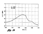
(b) 商業的にはライコム(Lycom)から入手可能であるDCF又は高負分散ファイバである。例えば、図3は、そのようなファイバに関する損失及び分散を示す。特に、1500nmでの分散は、およそ
D=−83ps/nm−kmである。
設計#1:スタンダード・ファイバを具備するファイバ・リンク
45kmの長さのリンクに関して、λ=1500nmでのリンクにおける合計分散
(D×L)LINK=(+14.4ps/nm−km)×(45km)
=+648ps/nm
である。
【0071】
ラマン増幅器における利得ファイバに関して、図3に記載のようなDCFを使用する場合、要求される利得ファイバの長さは
LLINK=(D×L)LINK/(−DDCF)=(648ps/nm)/
(83ps/nm−km)=7.8km
である。
【0072】
この長さは、ラマン増幅器において通常使用される典型的な長さである1キロメートルと比較して長い。
【0073】
要求される最小限の利得を計算するために、利得ファイバ及びリンク損失の挿入損失が計算される必要がある。DCFの損失はおよそ
αLGAIN=0.55dB/km×7.8km=4.3dB
である。
【0074】
1500nmでの伝送リンク損失はおよそ
αLLINK=0.22dB/km×45km=9.9dB
である。
【0075】
それゆえに前記ポンピング電力は、少なくとも
G>αLGAIN+αLLINK=14.2dB
の利得を供給するように調整されなければならない。
【0076】
利得ファイバにおいて、約1400ナノメートルのポンピング波長に関する損失(すなわち、1500nmの動作波長の上の一つのラマン・オーダ)を計算することも重要である。図3より、1500ナノメートルの外挿された損失値は、およそ0.8dB/kmである。それゆえに、利得ファイバにおけるポンピング損失は、およそ
αLPUMP=0.8dB/km×7.8km=6.24dB
である。これは、非線形処理に関する前記Leffを超えるので、前記利得ファイバは、双方向にポンピングされるか、又は前記利得ファイバの半分にされたものの二つが、個別にポンピングされなければならない。
設計#2:分散シフトファイバを具備するファイバ・リンク
45キロメートルの長さのリンクに関して、λ=1500ナノメートルでのリンクにおける合計分散に関して
(D×L)LINK=(−4.25ps/nm−km)×(45km)
=−191.25ps/nm
である。ラマン増幅器における利得ファイバに関して、スタンダードSMF−28を使用する場合、要求される利得ファイバの長さは
LLINK=(D×L)LINK/(−DSMF-28)=(−191.25ps/nm)/(−14.4ps/nm−km)=13.28km
である。この長さは、ラマン増幅器において通常使用される典型的な長さである1キロメートルと比較して、長い。
【0077】
要求される最小限の利得を計算するために、前記利得ファイバ及び前記リンク損失の挿入損失を計算する必要がある。スタンダード・ファイバにおける損失はおよそ
αLGAIN=0.22dB/km×13.28km=2.92dB
である。前記DSFにおける1500ナノメートルでの伝送リンク損失はおよそ
αLLINK=0.25dB/km×45km=11.25dB
である。それゆえに、前記ポンピング電力は少なくとも
G>αLGAIN+αLLINK=14.2dB
の利得を供給するように調整されなければならない。
利得ファイバにおいて、約1400ナノメートルのポンピング波長に関する損失を計算することも重要である。スタンダード・ファイバにおいて、1500ナノメートルでの損失値は、およそ0.5dB/kmである。それゆえに、利得ファイバにおけるポンピング損失は、およそ
αLPUMP=0.5dB/km×13.28km=6.64dB
である。これは、非線形処理に関する前記Leffを超えるので、前記利得ファイバは再度、双方向にポンピングされるか、又は前記利得ファイバの半分にされたものの二つが、個別にポンピングされなければならない。
【0078】
7.DMRA増幅器の好ましい実施形態
図4(a)は、分散管理ラマン増幅器を供給するための開ループ設計を使用する本発明の第一の実施形態を示す。開ループ設計は、最も簡単なDMRAであるが、それは高いポンピング電力を必要とするかもしれない。図4(a)に記載のDMRA増幅器において、光学信号は、入力ポート110から光学利得ファイバ100に入力される。光学利得ファイバ100は、ポンピングレーザ120及び150によって生成されるポンピング光によって、双方向にポンピングされる。前記利得ファイバ100は、信号及びポンピング波長の両方で、単一空間モードであり、前記利得ファイバは、説明されたすべての属性を所有する。増幅された信号は、出力ポート160を通して出力される。前記ポンピングは、信号波長を伝送するがポンピング波長に亘って結合する、波長分割伝送方式(WDM)を通して結合される。
【0079】
ポンピング光の揺らぎが前記増幅された信号に結合しないように、厳格な逆伝播ポンピング及び信号形状を有することがしばしば望ましい。図4(b)に記載の開ループ構造は、前記利得ファイバを二つの区分200及び210に分割することでこれを達成する。二つのポンピング(pump)240及び270は、各区分をポンピングするために使用され、及びWDM230及び260は、前記ポンピングにおいて結合するために使用される。さらに、各光学アイソレータ250は、WDM230において発生するかもしれない、270から240へのポンピング・エネルギの間の干渉を避けるために、前記二つの区分の間に配置される。
【0080】
図4(b)は前記二つの利得区分の間のアイソレータを使用するが、他の素子がその代わりに使用されることができるということが、明確であろう。例えば、利得等化素子及び/又は光学アド/ドロップ・マルチプレクサ(図1)が、前記アイソレータ(図4(C))の代わりに、又は一緒に使用されてもよい。アド/ドロップ・マルチプレクサと関連する、典型的には高い挿入損失のために、前記二つの区分におけるポンピングの間に、有効な絶縁が達成される。
【0081】
前記利得ファイバポンピングに関する交互の構成も、図4(d)に記載される。従来の特許(すなわち特許第5,623,508号及び第5,673,280号)も、前記アイソレータ周辺のポンピング分岐が使用される、アイソレータを使用した実行を説明していたことが認められる。しかしながら、より良い構成が図4(d)に記載される。ここで、前記利得ファイバは、二つの長さに分割され、前記ポンピングは第一のファイバへと導入され、前記信号が導入され及び抽出される前記ポンピングが分岐され、及び前記ポンピングは第二の利得ファイバに入る。前記アイソレータへの損害を避けるように、残りのポンピングを取り除くために任意のWDMが使用されてもよい。前記アイソレータは、前記二つの利得ファイバの間に配置される。従来技術に対する、この構成の長所は:
・前記第一の段は、低ノイズ前置増幅器である;
・前記信号パスにおける前記アイソレータはさらにノイズを低減する;
・前記第二の段は、電力増幅器であり、ポンピング電力を使い果たす;
・微弱信号がより高い利得を見てからのより良いノイズ値
・より良い利得飽和性能;及び
・二重レイリー散乱(Rayleigh scattering)の同じ防止
を含む。
【0082】
さらに、二段増幅器の中段において、アド/ドロップ・マルチプレクサ等の他の素子も配置されることができることが明確であろう。例えば、図4(e)は、前記中段での光学アド/ドロップ・マルチプレクサとともに、図4(d)に記載の二段設計を示す。また、図4(d)及び4(e)に記載の構成は、分散補償ファイバが、利得ファイバとして使用されていなくても、独自のものであり、効果的である。さらに、合成増幅器のノイズ値に大きな影響を与えることなく、電力増幅器利得を増加させるように、二段増幅器の第二の段に双方向ポンピングを有することも、望ましいかもしれない。これは、図4(f)に記載される。
【0083】
前記ポンピング電力の要求を低減するために、サニャック・ラマン・キャビティ等の広帯域キャビティが使用されることができる。図5は、双方向ポンピングを伴うサニャック・ラマン・キャビティ設計を使用するDMRAの実施形態を示す。図5を参照すると、前記DMRAのサニャック・ラマン・キャビティは、広帯域ミラ(broadband mirror)310及びラマン利得ファイバを具備するループ・ミラ(loop mirror)300及びそれに接続された光学カプラ(optical coupler)350によって形成される。前記サニャック・ラマン・キャビティ設計は、アメリカ合衆国特許第5,778,014号に記載され、この特許は、ここに参照のために採用されている。光学信号370は、入力ポート380を通して前記ラマン利得ファイバ300に入力される。ポンピングレーザ320は、結合手段330を通して前記ファイバ300をポンピングするポンピング光を生成する。前記光学信号は増幅され、及び出力ポート390を通して出力する。この構成においては、前記ポンピングは、本来的に前記利得ファイバ300に関して双方向であることが認められる。
【0084】
前記ラマン利得ファイバは、前記開ループ設計に関する上述のものとおなじ特性を有する。同様に、第一の実施形態で使用されるポンピングレーザは、この第二の実施形態で使用される。サニャックDMRAはさらに、偏光状態を制御するために、サニャック・ラマン・キャビティに偏光コントローラ(polarization controller)360をさらに含んでもよい。しかしながら、前記ファイバが偏光を維持される場合、前記偏光コントローラは必要ない。前記光学カプラ350は、少なくとも前記ポンピングと前記信号波長の下の一つのラマン・オーダ(Raman Order)との間で、公称で50:50である。前記結合手段300は、信号及び中間ラマン・オーダを伝送するが、前記ポンピングに亘って結合するWDMカプラである。さらに、前記入力ポート及び出力ポートの各々は、様々なポンピング・オーダを伝送するが、前記信号に亘って結合するWDMカプラを具備する。前記サニャック・ラマン・キャビティの重要な効果は、それが、様々なラマン・オーダのより静止したカスケードに通じる受動ノイズ減衰特性を有することである。特に、差動周波ノイズは、リジェクション・ポート385を通して出力される。
【0085】
前記DMRAの他の構成は、図6に記載のとおり、チャープ・ファイバ回折格子(chirped fiber grating)を伴う循環ループ・キャビティを使用する。前記循環ループ・キャビティ設計は、上述のアメリカ合衆国特許出願「循環ループ・キャビティにおけるラマン増幅に関するチャープ・ピリオド回折格子(Chirped Period Grating)」に記載されている。この特許出願は、参照のためにここに採用されている。図6に記載の構成は、二つの所望の目的を達成する。第一に、前記信号及びカスケード・ラマン・ポンピングは、逆伝播であり、クロストークを低減する。第二に、チャープ・ブラグ回折格子470は、波長制御のために前記ループに導入される。前記チャープ・ブラグ回折格子は、様々なラマン・カスケード・オーダで広帯域反射(broadband reflection)を供給する。このように、前記様々なカスケード・ラマン・オーダに関する波長が選択される一方で、次の各々のカスケードのオーダで広げられた帯域幅を許可するために、十分に広帯域の反射が供給される。
【0086】
前記チャープ・ブラグ回折格子470は、様々なラマン・オーダで帯域幅を調整する一方で、前記ファイバ挿入損失を低減することを可能にする。商業用の回折格子は、40乃至50ナノメートルの大きさの帯域幅のものが入手可能である。また、前記回折格子の周期性における長さ及び変形を調節することで、前記帯域幅を制御することができる。前記回折格子の各々の中央における前記ブラグ状態は、前記カスケード・ラマン・オーダの最大利得波長と一致する。しかしながら、ファイバ・ブラグ回折格子の一つの特徴は、それらが反射モードのみで動作することである。そして、前記回折格子は、前記サーキュレータ(circulator)460のポート2に導入される。
【0087】
光学サーキュレータ460は、一つの方向のみに、ポートからポートへと順番に光の方向を変える、非相互装置(non-reciprocal device)である。特定すれば、ポート1からの入力は、ポート2へと方向を変えられる。しかしながら、ポート2に入る逆信号は完全に、使用可能な信号として、ポート3に伝送される。ポート1及び3は、完全に絶縁される。光学サーキュレータは、偏光独立に、及び低挿入損失であるように作られる3ポート結合装置である。また、光学サーキュレータは、光学アイソレータ技術に基づいており、それはこの点で確立されている。
【0088】
前記サーキュレータ460は、前記ポンピング及びカスケード・ラマン・オーダ波長で適切に動作するのに十分広い帯域であるべきである。前記サーキュレータの二つのポート(ポート1及び3)は、ラマン利得ファイバ400及び410の長さによって接続される。このラマン利得ファイバは、上述のとおり、分散補償のすべての属性を有する。前記利得ファイバは、二つの区分に分割され、その各々は有効にポンピングされる。波長λpにおける前記ポンピング420及び440は、WDMカプラ430及び450を使用して、時計回りに導入される。これらのカプラは、前記ポンピング波長に亘って伝送する一方で、前記カスケード・ラマン・オーダ及び前記信号波長を通過する。前記ポンピング及び様々なカスケード・ラマン・オーダは、前記ループの周りを時計方向に循環する。
【0089】
前記信号は、前記ポンピング及び前記様々なカスケード・ラマン・オーダとは反対に、時計とは逆周りで、前記サーキュレータ・ループを渡る。前記信号490は、WDM480を使用して、前記ラマン利得ファイバの一端に導入され、及びWDM495を使用して前記ファイバの他の一端から除去される。これらWDMは、前記信号波長に亘って伝送する一方で、前記ポンピング及び前記カスケード・ラマン・オーダを通過する。
【0090】
8.ラマン増幅器を伴うWDMシステムに関する利得等化
多重波長WDMチャネルを伴うこれら実施形態のいずれかを使用するために、前記利得を等化するためのいくつかの手段を、前記増幅器の出力において含むことは、最も必要であろう。交替に、図4(c)に記載のとおり、前記利得等化は、二区分利得ファイバにおける中段アクセスに配置されることができる。この波長依存性又は前記利得帯域の非均一性は、単一チャネル伝送に対してほとんど影響を持たない。しかしながら、それは前記増幅器を、一連の増幅器を通して、多重チャネル・オペレーションに適さないものにする。異なる波長でのチャネルが一連の増幅器を通して伝播すると、それらは利得及び信号対ノイズの比に関して、それらの間の増加する不一致を集積する。利得均化素子を使用して、長い一連の増幅器の使用可能な帯域を、顕著に増加させることができる。例えば、前記DMRAは、異なるチャネルに対して利得等化を供給するために、利得均化素子がそれに続くことができる(図1を参照)。
【0091】
前記利得均化素子を実行することの問題は、要求されるフィルタ機能の複雑性によって決定され、それは前記利得スペクトルに適合するために必要とされるガウス又はフーリエの項(Gaussian or Fourier term)の数に従って特徴付けられることができる。例えば、典型的なEDFA利得帯域は、5つのガウスの項が使用可能な帯域に適合することを要求する(図7(a))。一方で、前記ラマン利得スペクトル(図7(b))は、もっと滑らかであり、たった二つのガウスの項を使用することで適度に適合されることができる。その結果ラマン増幅器に対する利得等化は、EDFAに対するものよりも単純である。
【0092】
利得均化フィルタ・タイプに対して、少なくとも4つのアプローチ(approach)がある。異なるアプローチ及びそれらの間のトレードオフ(trade-off)は、以下を含む:
・マッハ・ツェンダ干渉計。単純な機能。赤又は青色帯域フィルタに有用。ノッチ(notch)又は広帯域フィルタにはあまり有用ではない。
・格子装置。一連のカプラ及び遅延線。フーリエ級数(Fourier series)を使用して、ノッチ・フィルタ及び前記広帯域エルビウム・スペクトルに適合することができる。
・誘電フィルタ。広帯域及びノッチ・フィルタが可能である。フーリエ級数も同様である。
・長期回折格子。広帯域及びノッチ・フィルタが可能である。ガウス級数も同様である。
これらの選択のうち、マッハ・ツェンダ干渉計は、おそらく最も安く、最も簡単に作られる。それゆえに、図1に記載の前記利得等化素子60は、二つのマッハ・ツェンダ干渉計を使用して費用効果的に実行されることができる。
【0093】
9.DSファイバを使用した伝送リンクに関するWDMシステム
約1550ナノメートルのゼロ分散波長を伴う従来のDSファイバに基づいた伝送システムは、多重WDMチャネル及びEDFAを使用してそれらの容量を更新するときに、大きな問題に直面する。EDFAに関する利得帯域は、およそ1535乃至1565ナノメートルに及び、典型的には1540乃至1560ナノメートルの均された利得区分を伴う。4WMからのペナルティによって、前記ゼロ分散波長に近接した波長(すなわち、およそ1540乃至1560ナノメートル)は、WDMシステムには使用できない。それゆえに、EDFAの有用な帯域幅のほとんどは、伝送リンクにおいてDSFを使用する時は、WDM更新に対して使用できない。
【0094】
しかしながら、WDMシステムは、ゼロ分散波長から十分に離れた、「紫色帯域」(すなわち1430乃至1530ナノメートル)へと動くことによって、DSFに基づいた伝送システムにおいて実行されることができる。ラマン増幅器は、ここに説明された従来技術及びDMRAに基づいた設計を含む、この波長ウィンドウに利得を供給するために使用されることができる。紫色帯域におけるDSFに対する分散の有限の負の値のために、WDMシステムに関する主な非線形性ペナルティが管理される。すなわち、有限分散値のために、4WMはもう位相整合しない。また、オペレーションは、通常の分散状況(すなわち、D<0)なので、MIは前記伝送リンクにおいては避けられる。
【0095】
伝送線が分散管理されることができるように、DMRAを使用することはより効果的である。4WMを避けるために、局所分散が高い一方で、分散パルスの広がりを避けるために、前記リンクに亘る平均分散はおよそゼロである伝送システムを参照する。分散管理は、伝送線分散が、正と負の値の間の符号が変化することを要求し、一定の伝送スパンに亘る集積分散の打ち消し(cancellation)を可能にする。DSFに基づいた伝送システムにおいて、DMRAは、前記利得ファイバとしてスタンダード分散ファイバを使用することによって、分散管理を簡単に供給することができる。スタンダード・ファイバは大量需要がある成熟した商品であるので、これは前記利得ファイバの費用を低減させる追加的効果を有する。
【0096】
DSFリンクを伴う分散管理WDM伝送システムの例示的な設計が、図8(a)乃至8(c)に記載される。入力信号530及び出力信号540は、多重波長WDMチャネルであり、それらは典型的には100ギガヘルツ(又は0.8ナノメートル)で均一に間隔を置かれる。DSF510及びDMRA570のリンクを含む区分を伴う前記伝送線は、周期的である。例えば、前記DMRAは、1430乃至1530ナノメートルの紫色帯域において動作すると仮定され、及び前記利得ファイバは、スタンダード分散を都合よく有する。必要であれば、利得イコライザ580はまた、前記伝送線内に周期的に配置される。上述のとおり、利得イコライザは、マッハ・ツェンダ干渉計のたった一つ又は二つの段でもよい。前記利得イコライザは、各DMRAに沿って都合よく含まれることができる。
【0097】
図8(a)乃至8(c)は、この例示的なシステムにおける分散及び非線形性管理も示す。特に、前記局所分散は、伝送リンクにおいては負であるが、DMRAにおいては正である。前記DMRAに関する分散補償ファイバの適切な選択をすると、上述のとおり、前記集積分散は、前記WDM波長帯域の中間における各伝送区分において相殺するように作られることができる。
【0098】
10.多重帯域WDMシステムにおけるチャネルの対称的追加による利得傾斜の最小化
前記ファイバの帯域幅利用が増加すると、予想される主な問題は、前記ラマン効果から生じるエネルギ交換による、前記帯域にわたる利得傾斜である。特に、前記ラマン効果は、エネルギを、より短い波長からより長い波長にシフトする。また、前記ラマン利得は、およそゼロの周波数差から、13.2テラヘルツ(又は1550ナノメートルの波長周辺のおよそ100ナノメートル)でのそのピークに増加させる。それゆえに、前記ラマン効果は、小さな周波数差から13.2テラヘルツまでの周波数分離に間隔を置かれたWDMチャネルに重要であり、及びCWチャネルに関するエネルギ交換の大きさは、増加する周波数分離とともに増加する。また、上述の説明から、新しい波長帯域が加えられると、ラマン利得傾斜は、次第に重要な効果になることが明らかになるであろう。ラマンからの一次効果は、エネルギ交換であり、二次効果は、チャネル・クロストークであるかもしれない。
【0099】
今日の長距離のファイバ光学伝送システムは、エルビウムドープファイバ増幅器(erbium-doped fiber amplifier)(EDFA)を使用する。EDFAに関する従来の帯域(C帯域)は、およそ1530乃至1565ナノメートルであり、35ナノメートルの幅である。いくつかのスパンがカスケードされ、及び波長の数が増加すると、ラマン利得傾斜からの影響(すなわち、より短い波長におけるより少ない利得及びより長い波長におけるより多い利得)は、すでに認められている。前記傾斜は、前記システム帯域幅が増加するにつれて悪化すると思われる。
【0100】
帯域幅に対する要求が増え続けるにつれて、新しい波長帯域:長波長又はL帯域を加える方法がある。このL帯域は、およそ1565乃至1610ナノメートルに及ぶので、前記C及びL帯域の間のその結果の合計帯域幅は、およそ80ナノメートルになるであろう。前記より広い波長範囲は、ラマン利得のピークに近づき始めることが認められる。それゆえに、前記新しい帯域の追加は、すでに配置されたC帯域にわたる顕著なラマン利得傾斜を生じると思われる。
【0101】
ラマン利得傾斜変化を説明するための、多くのグループが、理論的及び実験的の両方で、前記効果を研究してきた。例えば、シーメンス(Siemens)のグループはC帯域のみ、及び結合されたC及びL帯域にわたる利得傾斜の効果を研究してきた(光学ファイバ通信会議 OFC1999年、サン・ディエゴ、カリフォルニア州、1999年2月、投稿論文WJ−6に掲載された、P.M.クルムリック、E.ゴットヴァルト、A.マイヤ、C.J.ヴァイスク及びG.フィッシャ、「双方向WDM伝送におけるチャネル電力バランスに対するSRSの影響」)。彼らは、以下の帯域を定義する:
「青色帯域」 − C帯域における1530乃至1545ナノメートル
「赤色帯域」 − C帯域における1545乃至1560ナノメートル
「高帯域」 − L帯域における1570乃至1605ナノメートル
図9(a)及び(b)は、前記C帯域のみに関する、シーメンスからの実験結果を示し(青色帯域から赤色帯域へのラマン利得傾斜)、及び前記最大変化は、前記帯域のどちらか半分にわたり、およそ1デシベルよりも小さい。一方で、図10は、L帯域追加を伴うC帯域に関するシーメンスの計算を示し、及びいずれかの帯域における最大変化は、4デシベルの大きさでもよい。
【0102】
新しい帯域が、現存する帯域における変化を要求することなく、及び現存する帯域への影響を最小化することなく導入されることができる場合、それは有効である。しかしながら、前記ラマン効果によって、現存するC帯域EDFAは、調整可能な利得傾斜を供給するための装置に後付けされなければならない。前記利得傾斜は、チャネルの数、前記チャネル間隔、前記スパン長、及び前記全体の帯域幅に依存するので、調整可能な利得傾斜を有することは価値がある。しかしながら、新しい帯域を追加する一方で現存するC帯域における変化を最小化することが、望ましいであろう。新しい「ノブ(knob)」は常に追加される新しい帯域へ導入されることができるが、現存する帯域から新しい特性を要求することは難しい。
【0103】
C帯域における変化を最小化するための帯域の対称的追加
C帯域における変化を最小化するための簡単な方法は、C帯域の短波長及び長波長サイドの両方に、対照的にチャネル又は帯域を追加することである。そして、より長い波長チャネルは、C帯域からエネルギを除去するかもしれないが、より短い波長チャネルは、前記エネルギを補給するであろう。前記利得傾斜のスロープは、有効電力のみに依存しているが、帯域の対称的追加は、利得変化のゼロ交差又は支点を、C帯域の中央に移動させることができる。
【0104】
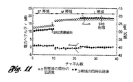
実験は、前記C帯域への変化を最小化するための、帯域の対称的追加の潜在的な効果を説明してきた。例えば、NTT未来ねっと研究所(NTT Network Innovation Laboratories)は、分散シフト・ファイバの100キロメートルに亘る3帯域伝送を実行した(光学ファイバ通信会議OFC1999年、サン・ディエゴ、カリフォルニア州、1999年2月、投稿論文WJ−2に掲載された、J.カニ、K.ハットリ、M.ジンノ、S.アイサワ、T.サカモト及びK.オグチ、「分散シフト・ファイバを通した三重波長帯域WDM伝送」)。図11は、三つの帯域を伴う彼らの実験結果を示す:より短い波長帯域が有効損失を受け、より長い波長帯域が利得を受ける一方で、前記C帯域(又は彼らが呼ぶところのM帯域)は、前記帯域にわたり最小の変化を有する。
【0105】
より特定的に、すでに配置されたファイバ及びそれらの低損失ウィンドウに適用される以下の帯域を説明する:
S+帯域:1430乃至1480ナノメートル
S帯域:1480乃至1530ナノメートル
C帯域:1530乃至1565ナノメートル
L帯域:1565乃至1610ナノメートル
EDFAは、C帯域及びL帯域のために存在する。しかしながら、より短い波長S帯域及びS+帯域に関しては、ラマン光学増幅器が使用されることができる。前記C帯域周辺の周波数又はエネルギに対照的に配置されるようにチャネルを追加する場合(すなわち、前記L帯域における一つのチャネル及び前記S帯域における対称チャネル)、前記ラマン利得傾斜からの効果は、C帯域において最小化されるであろう。
増幅器に対するラマン利得傾斜の影響
前の図から、前記S帯域は、ラマン・エネルギ交換による損失を補償するためだけよりも、光学増幅器からより多くの利得を必要とするであろうことが明らかであろう。同様に、損失を補償するためだけよりも少ない、前記L帯域光学増幅器からの利得が、ラマン・エネルギ交換のために必要とされるであろう。
【0106】
ほとんどのデジタル・システム(digital system)は、2.4Gb/sシステムに対して約20デシベルの信号対ノイズ(SNR)比を必要とする。同じSNRが三つすべての帯域に要求されるので、前記S帯域において必要とされるより高い利得はまた、前記S帯域光学増幅器に対して追加の要求をする。すなわち、より高い利得は通常、より多くのノイズ(すなわち、増幅された自然放出)を意味し、それはSNRに悪い影響を与える。S帯域及びC帯域において同じSNRを維持するための一つの方法は、S帯域におけるビット・レート(bit rate)を低減することである。交替に、同じSNRは、C帯域におけるよりもS帯域においてより低いノイズ値(NF)を伴う光学増幅器を使用することによって、維持されることができる。
【0107】
前記C帯域及びL帯域は、前記光学増幅器のためにEDFAを使用する。しかしながら、前記S帯域は、ラマン増幅器を使用することができる。原理上は、ラマン増幅器は、4段階様システムであるので、EDFAよりも低いノイズ値を有することができる。すなわち、前記ノイズ値は、N2/(N2−N1)に比例し、N2は上位キャリア密度(upper level carrier density)であり、N1は基底状態キャリア密度である。このパラメータは通常EDFAに関する1よりも大きい一方で、ラマン増幅器における1とおよそ等しい。
【0108】
前記S帯域に関する向上したNFを達成するための他の手段は、(次の項で説明されるとおり)分布ラマン増幅を使用することである。例えば、タイコ・サブマリン・システム(Tyco Submarine System)による実験(M.X.マ、H.D.キドルフ、K.ロットウィット、F.W.ケルフット、及びC.R.デビッドソン、「8×2.5Gb/sNRZ伝送を使用する5280キロメートルWDMシステム実験における240キロメートルのリピータ間隔(repeater spacing)」IEEEフォトニクス技術報告、第10巻、893乃至896ページ(1998年))は、分布増幅が、ディスクリート増幅器と比較して、NFにおける-2デシベルの低減又は向上を生じることを示す。各増幅器の場所にディスクリートS帯域増幅器を配置する代わりに、前記S帯域波長から−13.2テラヘルツ、波長が短いポンピングが導入されるであろう(すなわち、ポンピングは、1330ナノメートル乃至1430ナノメートルでよい)。
【0109】
前記C帯域周辺の新しいチャネルの対称的追加は、ラマン効果の一次影響を解決するだけであることが認められる−すなわち、前記利得傾斜は、エネルギ交換から生じる。チャネル間干渉からの第二の効果もあるかもしれない。これら第二の項は、チャネル間の十分な分散を保証することによって、小さく維持されることができるので、パターン依存クロストークを低減するために、チャネル間に十分なウォーク・オフ(walk-off)がある。
【0110】
11.多重帯域WDMシステムにおける分布ラマン増幅
上述の項は、新しい帯域が追加され、及び前記チャネル数が増加するにつれて、次第に重要になる4WM及びラマン利得傾斜からの非線形性減衰を説明した。これら非線形性減衰を最小化するための他の方法は、波長チャネル当たりの電力を低減することである。これは、分布ラマン増幅を使用することによって、レシーバにおける信号対ノイズ比のグラデーションなく達成されることができる。特に、分布ラマン増幅は、ラマン・オシレータ又はレーザ・ダイオードを伴う伝送線を構成するファイバを直接ポンピングすることによって、達成されることができる。前記ポンピング光は、前記伝送ファイバにおける固有ラマン利得を使用して、信号に対するラマン利得を生成する。前記利得は前記伝送線に固有であるので、これは現存するファイバ光学システムを更新する適切な手段を供給する。
【0111】
分布ラマン増幅は、前記ファイバにおける損失を取り消し又は補償するので、チャネル当たりの電力は低減されることができる。前記他の方法、分布ラマン利得は、そのディスクリート増幅器に相当するものよりも効果的により良いノイズ値を有する。前記チャネル電力は、非線形性が重要でなくなる点まで下げられることができる。例えば、典型的な伝送システムにおいて、チャネル当たり、0dBm(1mW)の電力はOC−48又は2.5Gb/sで使用され、6dBm(4mW)はOC−192又は10Gb/sで使用される。分布増幅を追加することで、OC−192システムは、−13dBm(0.05mW)くらい低いチャネル当たりの電力を伴い、実験室で実証された。
【0112】
分布ラマン増幅はまた、利得制御又は利得クランプ(gain clamping)にも役立つことができる。すなわち、チャネルが加えられ又は落とされる時、例えば光学アド/ドロップ・マルチプレクサが使用される時、前記利得レベルの変化を有することは望ましくない。チャネル当たりの電力は、顕著に低減されるので、この利得クランプ問題は、分布ラマン増幅を使用することによって、大幅に解決することができる。前記より低い電力は、無視できる利得すなわちポンピング枯渇があることを保証する。それゆえに、チャネル当たりの低電力と無視できる利得枯渇の組み合わせは、有効な利得クランプを供給する。
向上したノイズ値を示す計算
分布ラマン増幅は、伝送線における増幅器の有効ノイズ値を向上する。異なる増幅体系に対するノイズ値の例は、伝送長の関数(すなわち、周期的に増幅されるシステムにおける一つの期間の長さ)として図12乃至14に記載される。
【0113】
ヤリヴ(Yariv)は、彼の論文「周期的又は分布光学増幅を伴うファイバ・リンクにおける信号対ノイズの考察」(オプティクス報告、15巻、1064乃至1066ページ(1990年))において、信号対ノイズ比を計算する方法を説明した。E.デサビルは、彼の本「エルビウムドープファイバ増幅器、原則と応用」ジョン・ウィレー・アンド・サン、1994年の中で、分布増幅器を説明した。その方法体系の詳細は、デサビルの論文「ラマン活性ファイバ遅延線の論理と実践」(光波技術のIEEEジャーナル、1986年4月、426乃至443ページ)で見ることができる。しかしながら、この論文は双方向ポンピングを扱っておらず、前記信号及び前記ポンピングの両方に対する減衰定数が同じである場合のみを検討する。ヤリヴは、ポンピングの効果については一切触れていない。彼らの一般的なアプローチに続いて、我々は異なる減弱定数及び前方並びに後方ポンピングの変化する挿入を伴う双方向ポンピングの場合に関する一般的な場合の、閉形式の解決法を引き出すことができた。前記双方向の場合に関する我々の方法によって、前記前方並びに後方ポンピングに関する減衰定数は、前記信号のそれとは異なることができる。予想のとおり、我々の方法は、コンピュータを使用して評価される必要があるいくつかの積分を伴う。前記信号及びポンピング減衰定数が同じである場合には、我々はデサビルの公式に解析的に賛同するために、我々の一般的な式を削減することができた。双方向ポンピングの場合に関しては、我々の式は、交差点を前記伝送線の始まりにする、デサビルの後方ポンピングの場合へと削減する(すなわち後方ポンピングではない)。
【0114】
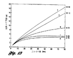
その結果が、いくつかの図に示される。図12は、前記信号及び前記ポンピングに関する減衰定数が同じである特別な場合に関して、我々のノイズ値が、デサビルが彼の本(図2.20、126ページ)で提示したものと同一であることを示すが、我々の最長の線の長さは、デサビルの最大の線の長さがたった50キロメートルであるのと比較して、80キロメートルである。前記減衰定数は、0.2デシベル/キロメートルと仮定される。この図には5つのグラフがある:それらはA、B、C、1、及び2が付けられている。曲線A及びCは、まとめられた増幅器の場合である:Aは前記線の始めにおける前記増幅器の場合で、前記線がその後に続く;Cは、その反対の場合で、すなわち線が最初で、それから増幅器、という場合である。曲線Bは、均一に分布した増幅に関する。一方で、グラフ1は前方分布ラマンポンピングに関し、及びグラフ2は後方分布ラマンポンピングに関する。図13は、前記ポンピング減衰定数が0.5デシベル/キロメートルであると仮定される一方で、前記信号減衰定数が0.2デシベル/キロメートルで維持されることを除いて、図12と同じである。この後半の状態は、ほとんどの現在配置されたファイバに関する現実により近い。
【0115】
これらの図から明らかであるとおり、ケースAは、最低ノイズ値を有し、及びケースCは最高値を有する(80キロメートル線で、それぞれ4.7デシベル及び18.96デシベル)。前記均一分布利得は、80キロメートルの長さで9.23デシベルのノイズ値(グラフB)を与え、それはケースA及びCの間である。前記増幅器によって導入されるノイズは、前記ファイバ伝送によっても減衰される一方で、より悪い場合(ケースC)においては、前記ノイズは、正に端部において導入されるので、第一の増幅器(ケースA)が最善である。前記ポンピング減衰定数を0.2デシベル/キロメートルから0.5デシベル/キロメートルに増加させる時、前記前方ラマン・ポンピングに関するノイズ値は、6.23デシベルから5.20デシベルに下がるが、前記後方ラマン・ポンピングに関しては、13.33デシベルから16.10デシベルに上がる。これは、前記ポンピング減衰が増加するにつれて、前記分布増幅器が、前記ディスクリート増幅器の場合により近づくからである。
【0116】
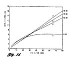
図14は、(1)前方ラマン・ポンピング、(2)後方ラマン・ポンピング、及び(3)双方向ラマン・ポンピングに関するノイズ値を示し、そのすべては0.2デシベル/キロメートルの減衰定数を有する。グラフ4は、0.5デシベル/キロメートルに設定されたポンピング減衰定数を有する双方向の場合に関する。双方向の場合に関しては、前記前方及び後方ポンピングの挿入が、前記線の部分の中間になると仮定する。80キロメートル部分での前記四つのグラフに関するノイズ値は、それぞれ6.23、13.33、15.00及び16.25デシベルである。前記グラフは、長距離を置いた、前記双方向の場合に関するノイズ値が、前記後方ポンピングの場合のそれよりも悪いことを示す。しかしながら、前記線の長さが小さい(40キロメートル以下である)場合、前記後方ポンピングされた場合に対していくつかの改良が可能である。デサビルによって指摘されたとおり、双方向ポンピングは、(改良されたノイズ値の可能性に加えて)二つの効果を有する:(1)両方のファイバの端部における低減された入力ポンピング電力と;及び(2)前記ファイバに沿ったより均一な媒体の反転であり、それは短いパルスを使用して高ビット・レートにおいて特に重要となりうる。
分布ラマン増幅を使用する実験
ファイバ伝送システムにおける前記非線形効果は、多くの最近の実験で説明された分布又は複合ラマン増幅の使用によって、避けることができる。例えば、NTT未来ねっと研究所における研究は、単一波長帯域におけるゼロ分散領域周辺のDSFでの伝送を実証した。特に、彼らは50ギガヘルツ間隔及び8×80キロメートルに対する10Gb/sを伴う32チャネルの高密度WDM(DWDM)伝送を実証する(N.タカチオ、H.スズキ、H.マスダ及びM.コガ、光学ファイバ通信会議OFC1999年、1999年2月、サン・ディエゴ、カリフォルニア州、締め切り後論文PD−9に掲載)。通常は、前記ゼロ分散波長の近隣におけるDWDMシステムは、4WMペナルティに苦しむ。しかしながら、分布ラマン増幅の使用を伴う−13dBmに前記チャネル電力を下げることによって、4WMは避けられ、及びその結果はDSFにおけるDWDM伝送の実施可能性を立証する。
【0117】
ほぼ同時に、ベル研究所/ルーセント・テクノロジーにおける他のグループが、単一波長帯域における4WM又は他の非線形性ペナルティのない、前記ゼロ分散波長に近いDWDM伝送を実証した(P.B.ハンセン、A.ステンツ、T.N.ニールセン、R.エスピンドラ、L.E.ネルソン及びA.A.アブラモヴ、光学ファイバ通信会議OFC1999年、1999年2月、サン・ディエゴ、カリフォルニア州、締め切り後論文PD−9に掲載)。彼らは、いくつかの実験をする:(a)25チャネル、10Gb/sチャネルの100ギガヘルツ間隔、8×83キロメートルの伝送;(b)49チャネル、10Gb/sチャネルの50ギガヘルツ間隔、4×83キロメートルの伝送である。かれらは、複合ラマン/エルビウムドープファイバ増幅器を使用することによって、DSFにおけるたった440mWのポンピング電力で、顕著な改善が得られるという結論に達する。
【0118】
これら二つの実験は、分布ラマン増幅が、単一帯域実験において効果的に、WDMチャネルの間の非線形効果を最小化することができるということを示す(すなわち、前記実験は、いわゆる「C帯域」又は1535乃至1565ナノメートルの従来の帯域においてのみ実施される。)しかしながら、多重帯域伝送が検討される時、帯域当たり一つ以上のポンピング波長に対する必要性があるであろう。この場合、ポンピング間の非線形相互作用は、異なる帯域における利得レベルでの大きな変化に通じうる。例えば、ポンピング間の前記ラマン効果は、より短い波長ポンピングからエネルギを奪って、より長い波長ポンピングに通じるであろう。この相互作用を最小化するために、それらの間の相互作用を最小化するように前記ポンピングを直交させる手段が必要とされる。
多重帯域の場合における分布ラマン増幅
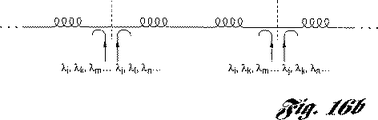
広帯域分布ラマン増幅において、異なる帯域に対するポンピング間の非線形相互作用は、交互の帯域ポンピングを空間的に分散することによって、及び/又は交互の帯域ポンピングを交差偏光することによって、最小化されることができる。一例として、すべてのLampに配置されディスクリート増幅器で周期的に増幅されたシステムを検討する。典型的には、前記増幅器の間隔は、Lamp=80キロメートルのオーダでもよい。いくつかの場合において、いくつかの中間点にアクセスがあってもよく、それは典型的には増幅器間のおよそ中間でもよい。分布ラマン増幅を追加することが望ましい。これは、ラマン・オシレータ又は前記伝送線をポンピングするためのレーザ・ダイオードのみを使用することによって、達成されることができる。増幅される必要がある多くの帯域があるかもしれないので:
λi=帯域iにおける利得に対するラマン・ポンピング波長(一つ以上のポンピング波長でもよい)
λj=帯域jにおける利得に対するラマン・ポンピング波長(一つ以上のポンピング波長でもよい)
i,k,m...一組のポンピング帯域
j,l,n...交互の組のポンピング帯域(すなわち上述の組から交互配置される)
を指定する。
【0119】
ディスクリート及び分布増幅器を具備する複合システムに関して、図15(a)乃至15(d)は、異なる波長帯域に対する前記ラマン・ポンピングを追加するための異なる構成を示す。図15(a)は、分布増幅が、逆伝播ラマン・ポンピングのみとともに追加され、及び中点段におけるアクセスが存在すると仮定する状況を示す。特に、交互の帯域ポンピングは、ポンピング間の非線形相互作用を最小化するために、異なる空間点に追加される。中スパン・アクセス(mid-span access)は利用可能ではないが、双方向ポンピングは可能である場合、図15(b)に記載の構成は使用されることができ、ポンピング間の相互作用を最小化するために、異なる方向に交互の帯域ラマン・ポンピングが着手される。双方向ポンピングが可能であり、及び中段アクセスも可能である場合、図15(c)に記載の構成を使用して、より均一なポンピングが達成されることができる。最後に、逆伝播ポンピングのみが可能であり、中段アクセスがない場合、前記交互ポンピング帯域が、図15(d)に記載のとおり、交互のポンピング帯域は、直交偏光に着手されることができる。この配列は、交差偏光された光に関するラマン利得が、順偏光された光に関するラマン利得の強さのおよそ10分の1であるという事実を利用する。図15(d)に記載の偏光多重伝送はまた、図15(a)乃至15(c)に記載の他の体系のいずれかと有利に結合されることができることが明らかであろう。
【0120】
上述の複合利得よりもむしろ、分布ラマン利得のみを使用することも、有利かもしれない。図16(a)乃至16(d)は、分布ラマン増幅のみに関する対応するポンピング構成を示す。再度、Lampの期間を伴う周期的に増幅されたシステムを仮定する。図16(a)は、中段アクセスが存在する純粋な逆伝播ポンピング体系を示す。前記交互のポンピング帯域は、この場合空間的に分散される。図16(d)は、中段アクセスがない双方向にポンピングされた状況を示し、交互のポンピングが、異なる方向に着手される。図16(c)は、より空間的に均一な利得を作るために、中段アクセスを加えた双方向ポンピングの組み合わせを示す。最後に、図16(d)は、交差偏光された交互のポンピング帯域の着手を示す。再度、図16(d)に記載の交差偏光されたポンピングは、図16(a)乃至16(c)に記載の構成のいずれかと有利に結合されることができる。
【0121】
要約すると、本発明の特徴は:
A) ラマン・アンプ(Raman amp)と結合された分散補償:
(1)前記利得ファイバが、伝送線に対する分散補償をするラマン・アンプ
(2)ファイバはポンピング及び信号に対する単一モードであり、前記ファイバに対する遮断波長が、前記ポンピング波長よりも短いことを意味する
(3)前記増幅器利得レベルは、前記ファイバ・リンクの一区分における損失と同様に、前記分散補償ファイバにおける損失の合計より大きいか又は等しく設定される
(4)前記利得ファイバの長さ及び分散は、前記増幅器の有効分散(D×L)ampが、前記ファイバ伝送リンク(D×L)Linkにおける有効分散をほぼ相殺するように選択される
(5)同じ素子における光学利得を供給する光学増幅器はまた、前記リンクの分散も補償する
(6)前記利得媒体は、レーザ・ダイオード又はラマン・オシレータによってポンピングされる分布利得媒体として機能するファイバである
(7)前記利得が、前記ファイバ・リンクにおける損失及び前記分散補償ファイバにおける損失をほぼ補償するように、前記ポンピングレベルは調整される
(8)前記ラマン・オシレータは、カスケードされたラマン・オシレータである
(9)前記ファイバは、分散補償ファイバである
(10)ファイバは、ポンピング及び信号に対して単一モードである(ファイバに対する遮断波長は、前記ポンピング波長よりも短い)
(11)前記ファイバ分散及び長さは、(D×L)Linkにほぼ等しくかつ反対である前記伝送リンク(D×L)ampにおける合計の分散を相殺するように選択される
(12)前記ファイバは、前記ポンピングに対して4Leffより小さい場合、一方向からポンピングされる
(13)前記ファイバの長さが、前記ポンピングに対する前記Leffを超える場合、前記ファイバは双方向にポンピングされることができる
(14)前記ファイバの長さが、前記ポンピングに対する前記Leffを実質的に超える場合、前記ファイバは二つのポンピングを有する二つの部分に分割されることができる。前記二つの増幅器区分は、アイソレータ、利得等化素子及び/又は光学アド/ドロップ・マルチプレクサによって結合されてもよい。
(15)前記利得ファイバが、伝送線に対して分散補償をするラマン・アンプ
(16)前記利得は、1390乃至1530ナノメートルの波長範囲である
(17)前記利得ファイバが分散補償ファイバであるラマン増幅器
(18)前記ファイバ伝送リンクの有効分散を補償するように選択される長さ及び分散を有するファイバ
(19)前記ファイバの長さが2Leffより大きい場合、それは双方向にポンピングされる
(20)前記ファイバの長さが2Leffより大きい場合、それは個別にポンピングされる二つの部分に分割される。前記二つの区分は、アイソレータ、利得等化素子及び/又は光学アド/ドロップ・マルチプレクサによって結合されてもよい
(21)図4、5、及び6に記載の特定の構成
B)DSFを伴う「紫色」帯域ラマン・アンプの使用
(1)分散シフト・ファイバの使用を具備し、及び1430乃至1530ナノメートルの波長範囲でのオペレーションを伴うファイバ・リンク・システム
(2)多重波長WDMシステムが、最小限の非線形性ペナルティで動作することができるように、ゼロ分散波長を避けるように選択された波長範囲
(3)前記1420乃至1530ナノメートルの範囲内の増幅器は、ラマン増幅器である
(4)前記ラマン増幅器における前記ファイバは、分散補償素子としても機能するように選択される
(5)前記1430乃至1530ナノメートルの範囲で動作するラマン増幅器を使用した、分散シフト・ファイバにおけるファイバ伝送システム
(6)前記システムは、多重チャネルWDMシステムである
(7)4WM及びパラメトリック増幅クロストークを低減するように選択された前記波長範囲
C)分散管理システムを伴うラマン・アンプの使用
(1)前記分散補償素子が、ラマン・ポンピングによってポンピングされる分散管理システム
(2)前記ラマンの利得レベルは、前記分散補償素子と同様に、前記ファイバ・リンクにおける損失を補償するように選択される
(3)前記分散補償素子は、一つのラマン・ポンピングでポンピングされることができ、又はL及びLeffに従って、双方向に又は二つの区分においてポンピングされることができる
(4)図8に記載の特定の構成
D)帯域の対称的追加
(1)前記C帯域における利得傾斜変化を最小化するために、前記L帯域におけるチャネルは、前記S帯域におけるチャネルにほぼ等しい数で追加される。(チャネル数に関して)前記ほぼ対称的なチャネル追加は、前記C帯域におけるラマン・エネルギ交換を相殺する
(2)前記S帯域における利得は、前記ラマン・エネルギ交換の責任を負うための線形損失を補償するために必要とされるよりも大きくなければならない。同様に、前記L帯域における利得は、線形損失を補償するために必要とされるよりも小さいべきである。
(3)前記C帯域及びS帯域における同じSNRを有するために、前記S帯域におけるビット・レートは下げられることができ、又は前記S帯域増幅器は、低ノイズ値を有する必要がある。
(4)前記S帯域における増幅器は、ラマン増幅器でもよく、それは前記増幅器の4段階性質により、より低いノイズ値を有することができる。
(5)前記ファイバに対する前記ゼロ分散波長は、十分なウォーク・オフがチャネル間干渉を最小化することができるようにするために、3つの帯域すべての外側に留められるべきである。
(6)前記C及びL帯域における増幅器が、ディスクリート増幅器でもよい一方で、前記S帯域増幅器は、向上したノイズ値を達成するために、分布増幅器でもよい。
(7)前記S帯域における分布ラマン増幅は、ディスクリート・レーザ・ダイオードを伴う前記伝送線をポンピングすることによって、又はラマン・オシレータによって達成されることができる。
E)多重帯域を伴う分布ラマン増幅
(1)多重帯域分散システムにおいて、ポンピング間の相互作用又はエネルギ交換を最小化するための、前記ポンピングを直交させる手段。
(2)広帯域分布ラマン増幅において、異なる帯域に対するポンピング間の非線形相互作用は、交互の帯域ポンピングを空間的に分散することによって及び/又は交互のポンピング帯域を交差偏光することによって、最小化されることができる。
(3)図15(a)乃至15(d)に記載の前記複合システム。
(4)図16(a)乃至16(d)に記載の前記分布システム。
(5)前記分布ラマン増幅は、ディスクリート・レーザ・ダイオードを伴う前記伝送線をポンピングすることによって、又はラマン・オシレータによって達成されることができる。
【0122】
本発明の実施形態が記載され及び説明されてきた一方で、これらの実施形態は、本発明のすべての可能性のある形式を記載し及び説明するものではない。むしろ、本明細書で使用される単語は、限定よりも説明のための単語であり、本発明の精神と範疇から逸脱することなく、様々な変更がなされてもよいことが理解される。
【図面の簡単な説明】
【図1】図1は、典型的な伝送システムを示す図であり、周期的に前記リンク素子内に、分散補償、光学増幅及び利得等化を供給する構成要素が挿入される。
【図2】図2は、1000ナノメートルのポンピング波長での石英に対する測定されたラマン利得スペクトル(spectrum)を示すグラフである。
【図3】図3は、大きな負の分散を有する分散補償ファイバ(DCF)に関する波長に対する典型的な分散及び損失を示すグラフである;特に、これらの特性はライコム(Lycom)製品で測定される。
【図4】図4(a)乃至4(f)は、前記DMRAに対する開ループ構成を示す図である;図4(a)においては、双方向にポンピングされた利得ファイバが使用され、図4(b)においては、前記利得ファイバは二つの部分に分割され、及び前記構成は前記ポンピング及び信号に対して逆伝播する;図4(b)に対する代替として、図4(c)は、利得等化フィルタ又は光学アド/ドロップ・マルチプレクサ等の他の素子が、前記増幅器の前記二つの区分の間に配置されてもよいことを示す;図4(d)は、前記ポンピングが前記第一の段の逆伝播へと挿入され、及び前記増幅器の第二の段に送られる、改良された二段増幅器を示す;図4(e)は、光学アド/ドロップ・マルチプレクサ等の中段素子を有する、図4(d)に記載の二段設計の他のバージョン(version)を示す;及び図4(f)は、前記合成増幅器に対するノイズ値における厳しい減衰なく、前記電力利得を上昇させるために、前記第二段において双方向ポンピングが使用される、図4(d)に記載の基本的設計のさらなる変形を示す。
【図5】図5は、サニャック・ラマン・キャビティに基づいたDMRAを示す図である。この構成に関する一つの特性は、それが前記利得ファイバの双方向ポンピングを自動的に有することである。
【図6】図6は、チャープ・ブラグ回折格子を有する循環ループ・キャビティに基づくDMRAのさらに他の設計を示す図である;前記循環ループ・キャビティは、前記信号及びラマンポンピングオーダが逆伝播する一方で、前記チャープ・ブラグ回折格子が波長制御を供給することを保証する。
【図7】図7(a)及び7(b)は、前記EDFA及びラマン利得帯域の、異なるガウス関数との適合を示すグラフである;図7(a)に記載の前記EDFA帯域が、5つのガウス関数を必要とする一方で、図7(b)に記載のラマン利得帯域は、二つのガウス関数で十分に概算されることができる。
【図8】前記伝送ファイバがDSファイバに基づいている、例示的な分散管理WDM伝送システムを示す、図8(a)は図であり、図8(b)及び(c)はグラフである。;例として、前記ラマン利得ファイバは、スタンダード分散ファイバでもよい;さらに多重波長に対して、利得イコライザは前記増幅器とともに周期的に配置されることができる。
【図9】図9(a)及び9(b)は、従来のC帯域(光学ファイバ通信会議 OFC1999年、サン・ディエゴ、カリフォルニア州、1999年2月、投稿論文WJ−6に掲載された、P.M.クルムリック、E.ゴットヴァルト、A.マイヤ、C.J.ヴァイスク及びG.フィッシャ、「双方向WDM伝送におけるチャネル電力バランスに対するSRSの影響」から引用)の青色及び赤色帯域に対する利得傾斜を示すグラフである。
【図10】図10(a)及び10(b)は、長波長L帯域(光学ファイバ通信会議 OFC1999年、サン・ディエゴ、カリフォルニア州、1999年2月、投稿論文WJ−6に掲載された、P.M.クルムリック、E.ゴットヴァルト、A.マイヤ、C.J.ヴァイスク及びG.フィッシャ、「双方向WDM伝送におけるチャネル電力バランスに対するSRSの影響」から引用)を補足される時の、前記従来のC帯域に対する利得傾斜を示すグラフである。
【図11】図11は、各帯域が個別に着手され及び三つすべての帯域が一緒に着手される時の、異なる帯域における電力ペナルティを示すグラフである(光学ファイバ通信会議OFC1999年、サン・ディエゴ、カリフォルニア州、1999年2月、投稿論文WJ−2に掲載された、J.カニ、K.ハットリ、M.ジンノ、S.アイサワ、T.サカモト及びK.オグチ、「分散シフト・ファイバを通した三重波長帯域WDM伝送」から引用)。
【図12】図12は、異なる場合に関するファイバ長に対する算出された光学ノイズ値を示すグラフである;前記ポンピング及び信号減弱の両方は、ファイバにおいて0.2デシベル/キロメートルになると仮定される;(A)ファイバの前の増幅器、(B)均一に分布した増幅器、(C)増幅器の前のファイバ、(1)前方ポンピングラマン増幅器、及び(2)後方ポンピングラマン増幅器である。
【図13】図13は、異なる場合のファイバ長に対する算出された光学ノイズ値を示すグラフである;図12においてより現実的であり、ここでは前記ポンピング減弱は、0.5デシベル/キロメートルと仮定される一方で、前記信号減弱は、前記ファイバにおいて0.2デシベル/キロメートルであると仮定される;(A)ファイバの前の増幅器、(B)均一に分布した増幅器、(C)増幅器の前のファイバ、(1)前方ポンピングラマン増幅器、及び(2)後方ポンピングラマン増幅器である。
【図14】図14は、異なる種類の分布ラマン増幅器のファイバ長に対する算出された光学ノイズ値を示すグラフである;(1)0.2デシベル/キロメートルのポンピング及び信号減弱を仮定する前方ポンピングラマン増幅器、(2)0.2デシベル/キロメートルのポンピング及び信号減弱を仮定する後方ポンピングラマン増幅器、(3)0.2デシベル/キロメートルのポンピング及び信号減弱の両方を仮定する双方向ポンピングラマン増幅器、及び(4)前記ポンピング減弱定数が、0.5デシベル/キロメートルであると仮定される点を除いて、(3)と同じ条件である双方向ポンピングラマン増幅器である。
【図15】図15(a)乃至15(d)は、ディスクリート及び分布増幅器を具備する複合システムを示す図である;図15(a)においては、分布増幅は、逆伝播ラマンポンピングのみが加えられ、中点段においてアクセスが存在すると仮定する;ポンピングの間の非線形相互作用を最小化するために、異なる空間点において交互の帯域ポンピングが加えられる;図15(b)においては、中スパン・アクセス(mid-span access)は使用できないが、双方向ポンピングは使用でき、ポンピングの間の相互作用を最小化するために、交互の帯域ラマンポンピングが異なる方向に着手されるこの構成が使用されることができる;図15(c)においては、双方向ポンピングが使用されることができ、中段アクセスも使用可能であり、この体系を使用してより均一なポンピングが達成されることができる;図15(d)においては、逆伝播ポンピングのみが使用されることができ、中段アクセスはなく、前記交互のポンピング帯域は、直交偏光されて着手されることができる;図15(d)に記載の前記偏光多重送信は、図15(a)乃至15(c)に記載の他の体系のいずれかと、有利に結合されることもできる。
【図16】図16(a)乃至(d)は、図15(a)乃至(d)に記載された複合利得よりもむしろ、分布ラマン利得のみを示す図である;図16(a)においては、中段アクセスが存在し、及びこの場合、前記交互のポンピング帯域は空間的に分散される純粋な逆伝播ポンピング体系が示される;図16(b)においては、交互のポンピングが異なる方向に着手される、中段アクセスがない双方向にポンピングされた状態が示される;図16(c)においては、より空間的に均一な利得を作るための、双方向ポンピングに中段アクセスを加えた結合が示される;図16(d)においては、交差偏光された交互のポンピング帯域の着手が示される;図16(d)に記載の交差偏光されたポンピングは、図16(a)乃至(c)に記載の構成のいずれかと有利に結合されることができる。[0001]
(Technical field)
The present invention relates generally to optical amplifiers used in fiber optics for telecommunications, cable television and other fiber optic applications. More specifically, the present invention provides an optical amplifier that also provides dispersion compensation for fiber optic links as well as a method for minimizing gain tilt and an apparatus for minimizing nonlinear interactions during band pumping. is connected with.
[0002]
(Background technology)
Bandwidth requirements continue to increase rapidly in fiber-optic superhighways due to applications such as data communications and the Internet. As a result, the bandwidth of the optical fiber can be increased by using faster speeds for each channel—so-called time division multiplexing systems—and multiple wavelengths of light—so-called wavelength-division multiplexing (WDM). A lot of effort is spent on leveraging width.
[0003]
Most of the fiber optic networks currently in use are two types of fiber: standard single-mode fiber (“standard” fiber) or dispersion-shifted fiber (DSF). Use one of them. Standard fibers have a zero dispersion wavelength of approximately 1310 nanometers, and the dispersion results primarily from the intrinsic glass dispersion. Most of the terrestrial networks in the United States and most of the world are actually based on standard fiber. On the other hand, in DSF, waveguide dispersion is used to shift the zero dispersion wavelength to a longer wavelength. A conventional DSF will have a zero dispersion wavelength at 1550 nanometers with minimal loss in fused silica fiber. However, the zero dispersion wavelength can be shifted by changing the amount of added waveguide dispersion. DSF is used only in two countries, Japan and Italy, as in the new long haul link.
[0004]
Constraining factors for fiber optic transmission lines include loss, dispersion and gain equalization. Loss refers to the fact that the signal is attenuated as it passes through the fiber due to other extrinsic effects such as intrinsic diffusion, absorption and loss. For example, an optical amplifier can be used to compensate for the loss. Dispersion means that light of different frequencies travels at different speeds, and it is due to both material properties and waveguiding effects. When using multi-wavelength systems, and due to frequency and gain non-uniformity, gain equalization is required to stabilize the gain across different wavelength channels.
[0005]
A typical solution to overcome these limitations is to place them periodically in the transmission system elements to compensate for each of these problems. For example, FIG. 1 shows that a
[0006]
Finally, the gain equalizer includes a Mach-Zehnder interferometer and a long-term diffraction grating. Rather than building a system from these individual components, it is easier to combine two or more of the functions described in FIG. 1 into a single component as described in US Pat. No. 5,887,093. Yes and may be more cost effective.
[0007]
Another problem that arises in WDM systems is the interaction between channels and crosstalk through nonlinearities in the fiber. In particular, four-wave mixing (4WM) causes energy exchange between different wavelength channels, but only 4WM is phase matched at near zero dispersion wavelength. As a result, it is difficult to operate a WDM system from approximately 1540 to 1560 nanometers if the fiber link is made from conventional DSF. Since typical EDFAs have a gain of 1535 to 1565 nanometers, this turns out to be very disappointing, and the more uniform gain band is approximately 1540 to 1560 nanometers. A second fiber nonlinearity that may be a problem is modulation instability (MI), which is 4WM, where the nonlinear refractive index of the fiber helps in phase matching. However, when the dispersion is positive or in the so-called soliton regime, only MI is phase matched. Therefore, MI can be avoided by operating at wavelengths shorter than zero dispersion wavelength.
[0008]
As bandwidth utilization increases for individual fibers, the number of bands used for transmission increases. For WDM systems that use many bands, additional complexity arises from the interaction between amplifications in a multi-band scenario. In particular, a specific system design is required for Raman amplification in a multiband transmission system. First, a new non-linearity penalty arises from the gain slope from the interchannel Raman effect. This occurs because long wavelength channels tend to take energy away from short wavelength channels. Therefore, a means for minimizing the gain slope on the existing channel with the addition of a new WDM channel is needed.
[0009]
To minimize the effects of both 4WM and Raman gain tilt, other technical means will use distributed Raman amplification. In a WDM system with multiple bands, complexity arises from the interaction between the different pumps along the transmission line.
[0010]
US Pat. No. 5,883,736 discloses an ER-doped optical fiber amplifier.
[0011]
U.S. Pat. No. 5,673,280 discloses an article comprising a low noise optical fiber Raman amplifier.
[0012]
U.S. Pat. No. 5,623,508 discloses an article comprising an inverse pumped fiber optic Raman amplifier.
[0013]
(Disclosure of the Invention)
It is an object of the present invention to combine dispersion compensation and optical amplifier functions through a single optical element, such as a Raman amplifier in which the amplifier gain fiber simultaneously performs the dispersion compensation.
Another object of the present invention is to provide different designs of the Raman amplifier depending on whether the fiber optic link is standard or uses DS fiber.
Yet another object of the present invention is that the WDM system avoids non-linearity constraints from 4WM and MI by using the "purple" band in a Raman amplifier with dispersion compensating fiber over a DS fiber link. Is to be able to.
[0014]
Yet another object of the present invention is to minimize the effect of gain tilt on existing conventional bands by the symmetrical addition of bands below and above existing bands. While the longer wavelength channel is amplified with an erbium-doped fiber amplifier, the shorter wavelength system may be advantageously amplified with a discrete or distributed Raman amplifier.
[0015]
Finally, yet another object of the present invention is to avoid fiber nonlinear effects in high density WDM systems by using distributed Raman amplification. In order to avoid interaction between pumping in a multi-band system, a means for orthogonalizing adjacent band pumping is described to minimize the interaction between pumping through Raman gain. Therefore, in order to reduce the interaction between pumping for different bands, means are provided to multiplex the pumping for different bands so that they are spatially, directional or polar orthogonal or non-overlapping. The
[0016]
In carrying out the above and other objects of the present invention in a fiber optic transmission system including at least one transmission link having length, optical loss, dispersion, sign of dispersion, and cutoff wavelength, the present invention provides a And a single optical element for compensating the optical loss. The optical element includes an input port for receiving an optical signal having a signal wavelength, a distributed gain medium having an optical loss and connected to the input port for amplifying the optical signal, and the optical signal A pumping wavelength for generating pumping light for pumping the distributed gain medium at a pumping level high enough to receive an effective gain to compensate for optical losses of the transmission link as well as the gain medium Including mechanism. The optical element further includes an output port for outputting the amplified optical signal.
[0017]
The distributed gain medium is typically a gain fiber having a sign of length, dispersion and dispersion. The gain fiber has a dispersion-length product that is substantially equal in size to the dispersion-length product of the at least one transmission link, excluding those of opposite sign. Also, the gain fiber has a cut-off wavelength shorter than the pumping wavelength so that the gain fiber is in a single spatial mode for both the pumping wavelength and the signal wavelength.
[0018]
The optical signal may be amplified in an open loop.
[0019]
The pumping mechanism may be at least one laser diode, Raman oscillator, or Raman wavelength shifter.
[0020]
In one embodiment, the gain fiber is pumped bi-directionally by the pumping mechanism.
[0021]
In another embodiment, the gain fiber has two separate sections, and the pumping mechanism pumps the two sections in back propagation.
The invention further includes an isolator, a gain equalization element and / or an optical add / drop multiplexer for connecting the two sections.
[0022]
In yet another embodiment, a pumping branch is coupled to the input and output ports for branching the pumping mechanism, and the gain fiber is a separate first and second divided by the input and output ports. And the pumping mechanism pumps the first section in back propagation and pumps the second section until the pumping mechanism force is exhausted.
[0023]
The optical signal may be amplified in a closed loop.
[0024]
The gain fiber may at least partially define a broadband cavity that is bi-directionally pumped by the pumping mechanism. In this case, the gain fiber may be a Raman gain fiber, and the broadband cavity may be a Sagnac Raman cavity.
[0025]
In another embodiment, the distributed gain medium includes a circular loop cavity having a chirped Bragg grating, and the gain fiber has two separate sections that are pumped in back propagation by the pumping mechanism.
[0026]
When the transmission line is a multi-wavelength transmission line having non-uniform gain across different wavelength channels, a second optical element is provided to equalize the non-uniform gain across the different wavelength channels. May be. The second optical element includes at least one stage of a Mach-Zehnder interferometer. The distributed gain mechanism may be a gain fiber having two separate sections, and the second optical element connects the two sections.
[0027]
In the transmission system operating in the violet band of 1430-1530 nanometers, wherein the at least one transmission link comprises a DSF having at least one fiber nonlinearity effect and zero dispersion wavelength, the single optical element comprises the at least one In one link, gain is provided in the violet band sufficiently away from the zero dispersion wavelength to avoid the at least one fiber nonlinearity effect. The gain fiber may be a standard dispersion fiber.
[0028]
The at least one fiber nonlinearity may be four-wave mixing and / or modulation instability.
[0029]
The at least one transmission link may have non-uniform gain across different wavelength channels, and the present invention further includes the single optical element for equalizing the non-uniform gain across the different wavelength channels A second optical element connected to the. The second optical element may include at least one stage of a Mach-Zehnder interferometer.
[0030]
The gain fiber may be a dispersion compensating fiber selected such that the integrated dispersion cancels substantially in the middle of the purple band.
[0031]
Further, in carrying out the above and other objects of the present invention, in a fiber optic multiband system including multiple wavelength transmission lines, when an additional band of wavelengths is added, it is within at least one existing band of wavelengths. A method is provided for minimizing the gain slope. The method includes both above and below the at least one existing band of wavelengths to obtain shorter and longer wavelength bands to minimize energy changes in at least one existing band of the wavelengths. Adding a substantially equal number of additional bands. The method also includes amplifying the shorter and longer wavelength bands such that each of the shorter and longer wavelength bands has gain.
[0032]
The step of amplifying the shorter wavelength band may be accomplished with either a discrete or distributed Raman amplifier.
[0033]
The step of amplifying the longer wavelength band may be accomplished with an erbium-doped fiber amplifier. The gain in at least one of the shorter wavelength bands is greater than the gain in at least one of the longer wavelength bands.
[0034]
The step of amplifying the shorter wavelength band may be in the form of a distribution.
[0035]
In addition, an apparatus is provided for carrying out the above and other objects of the present invention in a fiber optic multiband transmission system including multiple wave transmission lines. The apparatus includes a plurality of band pumps for pumping different bands of the transmission line to obtain amplification, and the band pumps for the different bands interact non-linearly by exchanging energy. The apparatus also includes means for orthogonalizing adjacent band pumping to minimize the non-linear interaction.
[0036]
The amplification may be distributed Raman amplification and the energy is Raman energy.
[0037]
Alternate band pumping may be spatially distributed to minimize the interaction between band pumping for the different bands.
[0038]
Alternate band pumping may be cross-polarized to minimize the interaction between band pumping for the different bands.
The plurality of band pumping may define a purely distributed system of distributed Raman amplifiers.
[0039]
Alternatively, the plurality of band pumping may define a combined system of discrete and distributed amplifiers.
[0040]
The plurality of band pumping may include a discrete laser diode or a Raman oscillator for pumping the transmission line.
[0041]
In accordance with the present invention, a Dispersion Managing Raman Amplifier (DMRA) is implemented using a gain fiber that also functions as a dispersion compensator. The fiber should be in single mode for both the pumping and signal wavelengths so that the cutoff wavelength is shorter than the pumping wavelength. The length and dispersion of the fiber should ideally have a dispersion-length product that is as large as the transmission link, but should have the opposite sign of dispersion. The pumping level should be selected to provide a gain that is greater than the sum of the losses from the dispersion compensating fiber and the transmission link. In addition, the pumping system is adapted to the pumping light.
It should be chosen to stay within the 3 dB loss length.
In one embodiment, a dispersion-compensating fiber (DCF) having a large negative dispersion (eg, D <−80 per second / nanometer-kilometer) is used for dispersion of the link using standard fiber. Used to compensate. If the fiber link is 45 kilometers long, the DCF should be about 7.8 kilometers long for dispersion compensation at 1500 nanometers. Also, the gain may exceed 14.2 decibels and the gain fiber may need to be pumped in both directions or in two sections.
[0042]
In other embodiments, standard fibers are used to compensate for link dispersion by using conventional DS fibers and operating in the “purple band”. If the fiber link is 45 kilometers long, the standard gain fiber should be about 13.3 kilometers long for dispersion compensation at 1500 nanometers. Also, the gain should exceed 14.2 dB, and the gain fiber may need to be pumped in both directions or in two sections.
[0043]
In embodiments where the gain fiber is divided into two sections, many elements can be used to connect the two sections. The simplest is to insert an isolator to avoid the interaction between the two pumps. Alternatively, a gain equalization element or optical add / drop multiplexer may be placed at the coupling point between the two sections.
[0044]
The invention also relates to implementing a dispersion and non-linearity managed fiber optic system that uses DS fiber in the transmission link. For multiwavelength WDM systems, operation in the “purple band” of 1430-1530 nanometers is required to avoid wavelengths very close to the zero dispersion wavelength in conventional DSFs. Gain is provided by a Raman amplifier, and the gain fiber also provides for dispersion compensation at the same time. Since 4WM is not phase matched away from the zero dispersion wavelength, the fiber nonlinearity is managed, and MI is avoided because the transmission fiber operates in normal dispersion (ie, D <0) situations.
[0045]
Combining the amplification and dispersion compensation elements simplifies the implementation of the system and is more cost effective for Raman amplifiers. Furthermore, a gain equalization element comprising one or two stages of a Mach-Zehnder interferometer can be used to level the gain band in the Raman amplifier. Also, there is an increasing interest in distributed management systems that alternate between positive and negative distributed segments with zero average variance across the link. This interest extends to virtually all data formats, including non-zero return, zero return and solitons. The Raman amplifier naturally leads to a dispersion and nonlinearity management system using a dispersion compensating fiber.
[0046]
Further, according to the present invention, the gain slope change over the conventional band currently used can be minimized by adding channels in the long wavelength band, approximately equal to the number of channels in the short wavelength band. . The approximately symmetrical channel addition (in terms of channel number) cancels the Raman energy exchange in the conventional band. The conventional and long wavelength bands can use erbium doped fiber amplifiers, while the short wavelength bands can be amplified by discrete or distributed Raman amplifiers.
[0047]
Finally, the invention also relates to distributed Raman amplification with multiple bands. In a multi-band distributed system, non-linear interaction between pumping for different bands can be minimized by spatially distributing alternating band pumping and / or by cross-polarizing alternating pumping bands. it can. Said distributed Raman amplification can be achieved by pumping the transmission line with a discrete laser diode or by a Raman oscillator.
[0048]
The above and other objects, features and advantages of the present invention will become readily apparent from the following detailed description of the best mode for carrying out the invention when considered in conjunction with the accompanying drawings.
[0049]
(Best Mode for Carrying Out the Invention)
The present invention advantageously combines the functions of optical amplification and dispersion compensation to simplify the implementation of a dispersion management system. The DMRA uses Raman amplification in a fiber whose dispersion compensates the surrounding transmission link.
[0050]
More specifically, the DMRA of the present invention has an input port for inputting an optical signal having a wavelength λ, receives the optical signal, amplifies the optical signal there through Raman diffusion, and spectrally. A distributed gain medium for spreading, a pumping means operated at a wavelength λP for generating pumping light for pumping the distributed gain medium, and outputting the amplified and spectrally spread optical signal And an output port. The dispersion and length of the distributed gain medium is selected to be a dispersion-length product of the same magnitude as the transmission link, excluding those with the opposite sign of dispersion. The fiber is made into a single spatial mode for the pumping and signal wavelengths by creating a cutoff wavelength of the gain fiber that is shorter than λP. The amplifier is also pumped such that the effective gain exceeds the total loss in the transmission link and dispersion compensating fiber.
[0051]
The first embodiment of the DMRA uses open loop amplification with an optical fiber gain medium. A pump source is used in which the fiber is pumped in two sections that are pumped bi-directionally or connected through an isolator. Alternatively, the two gain sections can be connected through a gain equalization element and / or an optical add / drop multiplexer. The second embodiment of the DMRA uses a Sagnac Raman cavity that is pumped and uses a dispersion compensating fiber in the loop. Feedback in the Sagnac Raman cavity reduces the required pumping force, and the broadband cavity design supports most of the generated bandwidth. The Sagnac Raman design also automatically achieves the bidirectional pumping. The third embodiment of the DMRA amplifier uses a circulating loop cavity with a chirped Bragg grating in which the fiber is pumped in two parts to maintain a strict back-propagation pumping scheme. The gain fiber length and dispersion in all of these embodiments depends on whether the transmission link uses standard fiber or DS fiber.
[0052]
The invention also relates to a dispersion and non-linearity management system in which the transmission link comprises a DSF. To achieve a multi-wavelength WDM system, the operation is selected to be within the “purple” band of 1430-1530 nanometers, thereby avoiding the wavelength region surrounding the zero dispersion wavelength. The gain fiber also uses DMRA for dispersion compensation. Even though the average dispersion across the link is adjusted to be approximately zero, the local dispersion is not small at any point in the fiber link. Thus, the 4WM penalty is removed because the 4WM is not phase matched. Also, since the operation is within the normal dispersion situation of the transmission fiber, the MI is also not phase matched.
[0053]
The present invention also relates to minimizing the gain slope to the existing conventional band by symmetric addition (in terms of number) of channels at longer and shorter wavelengths to the existing band. Symmetrically with respect to the short wavelength S band, the energy change in the conventional C band is minimized by adding a wavelength to the long wavelength L band. The C and L bands can be amplified with erbium-doped fiber amplifiers, while the S band can use discrete or distributed Raman amplifiers. The gain in the S band must be greater than the gain in the C band, and similarly, the C band may require more gain than the L band.
[0054]
Furthermore, the present invention relates to the use of distributed Raman amplification in a multiband system to reduce nonlinear fiber propagation effects. In wideband distributed Raman amplification, the non-linear interaction between pumping for different bands can be minimized by dispersing spatially alternating band pumping and / or by cross-polarizing alternating pumping bands. Can do. The orthogonality of adjacent band pumping can be done in a pure distribution system or a complex discrete / distribution system.
[0055]
In order to better understand the amplification mechanism and non-linearity operating in the present invention, we first describe stimulated Raman diffusion, Raman cascading, MI and 4WM. The stimulated Raman diffusion effect, MI and 4WM are the result of third-order nonlinearity that occurs when a dielectric material such as an optical fiber is exposed to intense light. The third-order nonlinear effect is proportional to the instantaneous light intensity.
[0056]
1. Stimulated Raman diffusion
Stimulated Raman diffusion is an important nonlinear process that makes optical fibers amplifiers and tunable lasers. Raman gain results from the interaction of optical phonons and strong light in quartz fibers, and the Raman effect is the transfer of energy from one optical beam (pumping) to another optical beam (signal). Leads to The signal is attenuated with respect to frequency (or increased with respect to wavelength) by an amount determined by the vibrational mode of the quartz fiber. The Raman gain coefficient gr for the quartz fiber is described in FIG. It should be noted that the Raman gain gr extends over a large frequency range (up to 40 terahertz) with a broad peak centered at 13.2 terahertz (corresponding to a wavelength of 440 cm −1). This behavior for the large frequency range is due to the amorphous nature of quartz glass, allowing the Raman effect to be used in broadband amplifiers. The Raman gain depends on the configuration of the fiber core and can vary with different dopant concentrations.
[0057]
Raman amplification has several attractive properties. First, Raman gain is a good candidate for updating existing fiber optic links because it is based on the interaction of optical phonons and pumping light in existing fibers. Second, there is no excess loss in the absence of pumping force, except for the loss of the inserted fiber, which is an important consideration for system reliability.
[0058]
2. Raman Cascade
Cascade is a mechanism by which optical energy at the pumping wavelength is converted into an optical signal at a longer wavelength through a series of nonlinear polarizations. Each nonlinear polarization of the dielectric generates a vibrational state of the molecule corresponding to a wavelength that is offset from the wavelength of the light that generated the stimulus. The nonlinear polarization effect is distributed throughout the dielectric, producing a series of cascaded wavelength shifts when energy at one wavelength pumps a vibration mode that produces light at a longer wavelength. This process can flow through many orders. The Raman gain feature has a peak centered at 13.2 terahertz in a silica fiber, so one Raman order can be organized to be separated from the previous order at 13.2 terahertz. it can.
[0059]
The cascade creates a highly desirable inductive Raman diffusion amplifier. Raman amplification itself has a very wide gain spectrum (a bandwidth greater than 5 terahertz with a peak around 13.2 terahertz), so multiple wavelengths or short optical pulses (as in wavelength division multiplex transmission). ) Can be used to amplify. Furthermore, the cascade allows Raman amplification over a wide range of different wavelengths. By changing the pumping wavelength or by using a cascaded order of Raman gain, the gain can be provided for the entire telecommunications window between 1300 nanometers and 1600 nanometers. .
[0060]
3. Modulation instability and four-wave mixing
MI / 4WM isStokes(S) and antiStokes(A) With two pumping (P) photons that generate photons. Both MI / 4WM and Raman amplification result from the third order susceptibility χ (3) in the optical fiber. More specifically, the real part of χ (3), the so-called nonlinear refractive index n2, is responsible for MI / 4WM, while the imaginary part of χ (3) associated with molecular vibration corresponds to the Raman gain effect. To do. In the quartz fiber, about 4/5 of the n2 is an electronic and instantaneous nonlinearity caused by ultraviolet resonance, and about 1/5 of the n2 is, for example, an optical phonon (MN Islam, Resulting from Raman-active vibrations such as ultrafast fiber switch devices and systems, Cambridge University Press, see more details in 1992). The imaginary part of this latter contribution corresponds to the Raman gain spectrum described in FIG.
[0061]
As in Raman amplification, MI / 4WM gain is present in all fibers. However, unlike the Raman effect, both MI and 4WM require phase matching. 4WM is usually not important in long fibers because it requires phase matching unless the operation is close to zero dispersion wavelength. However, since nonlinear refractive index is used to phase match the pumping and sidebands, MI can function as a self-phase match. This is especially true when manipulating near zero dispersion wavelengths in the fiber. In 4WM, when the signal wavelength enters a normal dispersion situation (where the signal wavelength is shorter than the zero dispersion wavelength), a waveband is generated without gain. MI is a 4-photon or parametric amplification whose nonlinear refractive index is used to phase match the signal and waveband. For MI, the pumping wavelength must be in an anomalous group velocity situation (i.e., the signal wavelength is longer than the zero dispersion wavelength), and proper phase matching ensures that the signal and waveband are forward propagated ( co-propagating).
[0062]
4). Distributed and nonlinear management transmission system
Until recently, prior knowledge was that maximum system bandwidth would occur for operation with approximately zero dispersion wavelength in the fiber. However, for WDM systems, this idea has been found to be wrong when nonlinearities are taken into account. When the system operates at or near the zero dispersion wavelength of the fiber, signal and amplifier noise in adjacent wavelength channels travels at a similar rate. Under these conditions, the multi-wavelength signal and noise have a long interaction length and can be mixed.
[0063]
Due to chromatic dispersion, different wavelengths travel through the transmission fiber at different group velocities. Chromatic dispersion can reduce phase-matching or propagation distances where adjacent wavelengths overlap, and can reduce the amount of interaction through nonlinear exponents in the fiber. Thus, in long transmission systems, the non-linear behavior is achieved by adjusting the integrated dispersion so that the length of phase matching is reduced and the end-to-end dispersion is reduced. Can be managed. This technique is known as dispersion mapping (for details, see Fiber Optic Telecommunications IIIA, IP Kamino and TL Cook, Academic Publishing,
[0064]
In dispersion mapping, dispersion compensation elements are periodically inserted into the transmission line in order to cancel integrated dispersion. By using DMRA, the periodicity of the dispersion compensation is the same as the periodicity of the amplifier interval. It is noted that for WDM systems, the integrated dispersion returns to zero for only one wavelength that is close to the mean zero dispersion wavelength for the transmission line. The different integrated dispersion for this WDM channel results from the nonzero slope of the dispersion curve. This is avoided only if the dispersion compensation element has the opposite sign of the dispersion slope from the transmission fiber (not just the opposite sign of dispersion). Except for this case, in order to minimize the signal dispersion, the integrated dispersion for the channels away from the canceling wavelength can be compensated with the opposite dispersion on the receiving side.
[0065]
5). Distributed management Raman amplifier
DMRA combines the amplification and dispersion compensation functions by using the dispersion compensating fiber as a gain fiber in a Raman amplifier. The cutoff wavelength of the gain fiber must be adjusted to be shorter than the pumping wavelength so that the pumping and signal are single mode. By operating away from the zero dispersion wavelength of the transmission fiber and the gain fiber, dispersion and nonlinearity management is achieved because the 4WM is not phase matched.
[0066]
The means of the present invention is an appropriate selection of gain fiber characteristics. In particular, the dispersion at the average optical wavelength multiplied by the length of the amplification fiber (D × L)GAINHowever, the fiber used in the Raman amplifier is selected so that it substantially compensates for the dispersion integrated in the link (preferably within 10 percent of the magnitude of the peak integrated dispersion value). Ie
(D × L)GAIN≒-(D × L)LINK
It is.
[0067]
This shows a few things:
The sign of dispersion for the amplification fiber is opposite to that of the transmission link fiber.
The dispersion value D in the amplification fiber is determined by the operating wavelength and the zero dispersion wavelength in the gain fiber.
The length of the fiber can be adjusted to provide the desired dispersion compensation.
If the transmission fiber is a standard fiber, the gain fiber can potentially lead to effective Raman gain. This is because so-called DCF (or large negative dispersion fibers) typically have a small core size and effective area, and an effective germanium content in the core, both of which contribute to a large Raman effect. .
The only condition is that the overall or average variance x length value for the transmission link segment is offset. That is, if desired, different fiber sections can be coupled within the Raman amplifier to achieve dispersion compensation.
It is important to understand that since the Raman gain is a non-linear process that depends on the pumping strength, gain is achieved only while the pumping strength remains high. For example, the effective length for Raman amplification is
![]()
α [dB / km] = 4.34 × α [km-1]
Is related to this decay constant by Therefore, the effective length for Raman gain is approximately the distance that the pumping intensity falls to half that intensity at the fiber input. If the effective loss at the pumping wavelength is approximately 6 to 7 decibels, the Raman gain is achieved by pumping the fiber bi-directionally or by splitting the fiber in half and pumping each half in half. Can be done.
[0068]
Finally, for proper loss compensation, the pumping power applied to the Raman amplifier is sufficient to compensate for the transmission link loss, the gain fiber loss and the associated coupler or splitter losses. There must be. For example, if the effective gain is given by G and the loss is denoted as the attenuation factor αL,
G [dB] ≧ αLLINK[DB] + αLGAIN FIBER[DB] +
αLCOUPLING & SPLITTING[DB]
It is.
[0069]
6). DMRA exemplary design for standard and DS fiber
To illustrate the DMRA concept, an exemplary system design in a transmission system that uses both standard and DS fibers is selected. To be specific, the following assumptions are made regarding the wavelength, link fiber, amplifier spacing, and gain fiber in the Raman amplifier:
·wavelength. Raman amplifiers have been developed for the purple band extending from 1430 to 1530 nanometers. In particular, the blue-violet band is 1430-1480 nanometers, while the red-violet band is 1480-1530 nanometers. As a specific example, a wavelength of λ = 1500 nanometers is used in the following example, which falls near the middle of the magenta band.
• Dispersion for standard single mode fiber. The standard fiber used is assumed to be Corning SMF-28, whereas the manufacturer:
1200 ≦ λ ≦ 1600nm
S0≦ 0.092ps / nm2-Km
At λ = 1500 nm, D≈ + 14.4 ps / nm-km
Supply dispersion.
• Dispersion for DS fiber. The DSF used is assumed to be Corning SMF / DS, whereas the manufacturer:
D (λ) ≈S0{λ−λ0} [Ps / nm-km]
1500 ≦ λ ≦ 1600nm
λ0≒ 1550nm (nominal)
S0≦ 0.085ps / nm2-Km
At λ = 1500 nm, D≈−4.25 ps / nm-km
Supply dispersion.
[0070]
・ Link length. Amplifier spacing is LLINK= 45 km, which is
A typical hut spacing in fiber optic networks.
-Gain fiber. The gain fiber must always have a cutoff wavelength shorter than the pumping wavelength. Possible candidates for gain fibers include (but not exactly these fibers, but fibers with similar dispersion characteristics):
(A) Standard SMF-28 fiber with 1500 nm and D = 14.4 ps / nm-km
(B) DCF or high negative dispersion fiber, commercially available from Lycom. For example, FIG. 3 shows the loss and dispersion for such a fiber. In particular, the dispersion at 1500 nm is approximately
D = −83 ps / nm-km.
Design # 1: Fiber link with standard fiber
For a 45 km long link, the total dispersion in the link at λ = 1500 nm
(D × L)LINK= (+ 14.4 ps / nm-km) × (45 km)
= +648 ps / nm
It is.
[0071]
For a gain fiber in a Raman amplifier, when using a DCF as shown in FIG. 3, the required gain fiber length is
LLINK= (D × L)LINK/ (-DDCF) = (648 ps / nm) /
(83 ps / nm-km) = 7.8 km
It is.
[0072]
This length is long compared to the one kilometer that is typically used in Raman amplifiers.
[0073]
In order to calculate the required minimum gain, the insertion loss of gain fiber and link loss needs to be calculated. DCF loss is approximately
αLGAIN= 0.55 dB / km x 7.8 km = 4.3 dB
It is.
[0074]
Transmission link loss at 1500nm is approximately
αLLINK= 0.22 dB / km x 45 km = 9.9 dB
It is.
[0075]
Therefore, the pumping power is at least
G> αLGAIN+ ΑLLINK= 14.2 dB
Must be adjusted to provide a gain of.
[0076]
It is also important to calculate the loss for a pump wavelength of about 1400 nanometers (ie, one Raman order above the 1500 nm operating wavelength) in a gain fiber. From FIG. 3, the extrapolated loss value of 1500 nanometers is approximately 0.8 dB / km. Therefore, the pumping loss in the gain fiber is approximately
αLPUMP= 0.8 dB / km × 7.8 km = 6.24 dB
It is. This is the L for non-linear processing.effThe gain fiber must be pumped bi-directionally, or two of the gain fiber halves must be pumped separately.
Design # 2: Fiber link with dispersion-shifted fiber
For a 45 km long link, with respect to the total dispersion in the link at λ = 1500 nanometers
(D × L)LINK= (-4.25 ps / nm-km) x (45 km)
= -191.25 ps / nm
It is. For standard gain fibers in Raman amplifiers, when using standard SMF-28, the required gain fiber length is
LLINK= (D × L)LINK/ (-DSMF-28) = (− 191.25 ps / nm) / (− 14.4 ps / nm-km) = 13.28 km
It is. This length is long compared to 1 kilometer, which is a typical length commonly used in Raman amplifiers.
[0077]
In order to calculate the required minimum gain, it is necessary to calculate the insertion loss of the gain fiber and the link loss. The loss in standard fiber is approximately
αLGAIN= 0.22 dB / km × 13.28 km = 2.92 dB
It is. Transmission link loss at 1500 nanometers in the DSF is approximately
αLLINK= 0.25 dB / km × 45 km = 11.25 dB
It is. Therefore, the pumping power is at least
G> αLGAIN+ ΑLLINK= 14.2 dB
Must be adjusted to provide a gain of.
It is also important to calculate the loss for a pump wavelength of about 1400 nanometers in a gain fiber. For standard fibers, the loss value at 1500 nanometers is approximately 0.5 dB / km. Therefore, the pumping loss in the gain fiber is approximately
αLPUMP= 0.5 dB / km × 13.28 km = 6.64 dB
It is. This is the L for non-linear processing.effThe gain fiber must be pumped in both directions again, or two of the gain fiber halves must be pumped separately.
[0078]
7). Preferred embodiment of DMRA amplifier
FIG. 4 (a) shows a first embodiment of the present invention that uses an open loop design to provide a dispersion managed Raman amplifier. An open loop design is the simplest DMRA, but it may require high pumping power. In the DMRA amplifier illustrated in FIG. 4A, an optical signal is input from the
[0079]
It is often desirable to have a strict backpropagation pumping and signal shape so that fluctuations in the pumping light do not couple to the amplified signal. The open loop structure described in FIG. 4 (b) achieves this by dividing the gain fiber into two
[0080]
Although FIG. 4 (b) uses an isolator between the two gain sections, it will be clear that other elements can be used instead. For example, gain equalization elements and / or optical add / drop multiplexers (FIG. 1) may be used in place of or in conjunction with the isolator (FIG. 4C). Due to the typically high insertion loss associated with add / drop multiplexers, effective isolation is achieved during pumping in the two sections.
[0081]
An alternate configuration for the gain fiber pumping is also described in FIG. It will be appreciated that prior patents (i.e., patents 5,623,508 and 5,673,280) have also described implementations using isolators where pumping branches around the isolator are used. However, a better configuration is described in FIG. Here, the gain fiber is divided into two lengths, the pumping is introduced into a first fiber, the pumping into which the signal is introduced and extracted is branched, and the pumping is into a second Enter the gain fiber. Any WDM may be used to remove the remaining pumping so as to avoid damage to the isolator. The isolator is disposed between the two gain fibers. The advantages of this configuration over the prior art are:
The first stage is a low noise preamplifier;
The isolator in the signal path further reduces noise;
The second stage is a power amplifier, which uses up pumping power;
-A better noise value after a weak signal sees a higher gain
-Better gain saturation performance; and
-Same prevention of double Rayleigh scattering
including.
[0082]
Furthermore, it will be clear that other elements such as add / drop multiplexers can also be arranged in the middle stage of the two-stage amplifier. For example, FIG. 4 (e) shows the two-stage design described in FIG. 4 (d) with the optical add / drop multiplexer in the middle stage. Further, the configurations described in FIGS. 4D and 4E are unique and effective even if the dispersion compensating fiber is not used as a gain fiber. Furthermore, it may be desirable to have bi-directional pumping in the second stage of the two-stage amplifier so as to increase the power amplifier gain without significantly affecting the noise value of the composite amplifier. This is described in FIG. 4 (f).
[0083]
To reduce the pumping power requirement, a broadband cavity such as a Sagnac Raman cavity can be used. FIG. 5 shows an embodiment of a DMRA that uses a Sagnac Raman cavity design with bi-directional pumping. Referring to FIG. 5, the DMRA Sagnac Raman cavity includes a
[0084]
The Raman gain fiber has the same characteristics as described above for the open loop design. Similarly, the pumping laser used in the first embodiment is used in this second embodiment. The Sagnac DMRA may further include a polarization controller 360 in the Sagnac Raman cavity to control the polarization state. However, if the fiber is kept polarized, the polarization controller is not necessary. The
[0085]
Another configuration of the DMRA uses a circulating loop cavity with a chirped fiber grating as described in FIG. The circular loop cavity design is described in the aforementioned US patent application “Chirped Period Grating for Raman amplification in the circular loop cavity”. This patent application is hereby incorporated by reference. The configuration described in FIG. 6 achieves two desired objectives. First, the signal and cascaded Raman pumping are backpropagating and reduce crosstalk. Second, a chirp-Bragg grating 470 is introduced into the loop for wavelength control. The chirped Bragg grating provides broadband reflection in various Raman cascade orders. In this way, the wavelength for the various cascaded Raman orders is selected, while a sufficiently wide band reflection is provided to allow bandwidth expanded in the order of each subsequent cascade.
[0086]
The chirped Bragg grating 470 allows the fiber insertion loss to be reduced while adjusting the bandwidth in various Raman orders. Commercial diffraction gratings are available with bandwidths ranging from 40 to 50 nanometers. Further, the bandwidth can be controlled by adjusting the length and deformation in the periodicity of the diffraction grating. The Bragg state at the center of each of the diffraction gratings corresponds to the maximum gain wavelength of the cascade Raman order. However, one feature of fiber Bragg gratings is that they operate only in reflection mode. The diffraction grating is introduced into
[0087]
The
[0088]
The
[0089]
The signal traverses the circulator loop counterclockwise as opposed to the pumping and the various cascaded Raman orders. The
[0090]
8). Gain equalization for WDM systems with Raman amplifiers
In order to use any of these embodiments with multiple wavelength WDM channels, it would be most necessary to include some means at the output of the amplifier to equalize the gain. Alternatively, as described in FIG. 4 (c), the gain equalization can be arranged in a middle access in a bisection gain fiber. This wavelength dependence or non-uniformity of the gain band has little effect on single channel transmission. However, it makes the amplifier unsuitable for multi-channel operation through a series of amplifiers. As channels at different wavelengths propagate through a series of amplifiers, they accumulate increasing discrepancies between them in terms of gain and signal-to-noise ratio. Using gain leveling elements, the usable bandwidth of a long series of amplifiers can be significantly increased. For example, the DMRA can be followed by a gain leveling element to provide gain equalization for different channels (see FIG. 1).
[0091]
The problem of implementing the gain leveling element is determined by the complexity of the required filter function, which is the Gaussian or Fourier term needed to fit the gain spectrum. Can be characterized according to number. For example, a typical EDFA gain band requires that five Gaussian terms fit into the usable band (FIG. 7 (a)). On the other hand, the Raman gain spectrum (FIG. 7 (b)) is smoother and can be reasonably adapted by using only two Gaussian terms. As a result, gain equalization for Raman amplifiers is simpler than for EDFAs.
[0092]
There are at least four approaches to the gain leveling filter type. Different approaches and the trade-off between them include:
・ Mach-Zehnder interferometer. Simple function. Useful for red or blue bandpass filters. Not very useful for notch or broadband filters.
・ Lattice device. A series of couplers and delay lines. A Fourier series can be used to fit the notch filter and the broadband erbium spectrum.
-Dielectric filter. Wideband and notch filters are possible. The same applies to the Fourier series.
・ Long-term diffraction grating. Wideband and notch filters are possible. The same applies to the Gaussian series.
Of these choices, the Mach-Zehnder interferometer is probably the cheapest and easiest to make. Therefore, the
[0093]
9. WDM system for transmission links using DS fiber
Transmission systems based on conventional DS fibers with a zero dispersion wavelength of about 1550 nanometers face major problems when updating their capacity using multiple WDM channels and EDFAs. The gain band for EDFAs ranges from approximately 1535 to 1565 nanometers, typically with a leveled gain section of 1540 to 1560 nanometers. Due to the penalty from 4WM, wavelengths close to the zero dispersion wavelength (ie approximately 1540 to 1560 nanometers) cannot be used for WDM systems. Therefore, most of the useful bandwidth of EDFA cannot be used for WDM updates when using DSF in the transmission link.
[0094]
However, WDM systems can be implemented in DSF-based transmission systems by moving to the “purple band” (ie, 1430-1530 nanometers), well away from the zero dispersion wavelength. A Raman amplifier can be used to provide gain to this wavelength window, including the prior art and DMRA based designs described herein. Because of the finite negative value of dispersion for the DSF in the purple band, the main nonlinearity penalty for WDM systems is managed. That is, due to the finite dispersion value, 4WM is no longer phase matched. Also, since the operation is a normal distribution situation (ie, D <0), MI is avoided in the transmission link.
[0095]
It is more effective to use DMRA so that the transmission line can be distributed and managed. To avoid 4WM, reference is made to a transmission system in which the local dispersion is high while the average dispersion across the link is approximately zero in order to avoid spread of the dispersion pulses. Dispersion management requires that transmission line dispersion requires the sign to change between positive and negative values, allowing for cancellation of integrated dispersion over a certain transmission span. In a transmission system based on DSF, DMRA can easily provide dispersion management by using a standard dispersion fiber as the gain fiber. Since standard fiber is a mature product with high demand, this has the added benefit of reducing the cost of the gain fiber.
[0096]
An exemplary design of a distributed management WDM transmission system with a DSF link is described in FIGS. 8 (a) -8 (c).
[0097]
FIGS. 8 (a) -8 (c) also illustrate dispersion and nonlinearity management in this exemplary system. In particular, the local dispersion is negative in the transmission link but positive in the DMRA. With appropriate selection of dispersion compensating fiber for the DMRA, as described above, the integrated dispersion can be made to cancel at each transmission segment in the middle of the WDM wavelength band.
[0098]
10. Minimization of gain tilt by symmetrical addition of channels in multi-band WDM systems
As the bandwidth utilization of the fiber increases, the main anticipated problem is gain slope across the band due to energy exchange resulting from the Raman effect. In particular, the Raman effect shifts energy from shorter wavelengths to longer wavelengths. The Raman gain also increases from a frequency difference of approximately zero to its peak at 13.2 terahertz (or approximately 100 nanometers around the 1550 nanometer wavelength). Therefore, the Raman effect is important for WDM channels spaced from small frequency differences to 13.2 terahertz frequency separation, and the magnitude of energy exchange for CW channels increases with increasing frequency separation. To do. It will also be clear from the above description that the Raman gain slope becomes increasingly important as new wavelength bands are added. The primary effect from Raman is energy exchange and the secondary effect may be channel crosstalk.
[0099]
Today's long-distance fiber optic transmission systems use erbium-doped fiber amplifiers (EDFAs). The conventional band (C band) for EDFA is approximately 1530 to 1565 nanometers and is 35 nanometers wide. As several spans are cascaded and the number of wavelengths increased, the effects from Raman gain tilt (ie, less gain at shorter wavelengths and more gain at longer wavelengths) have already been observed. The slope appears to worsen as the system bandwidth increases.
[0100]
As the demand for bandwidth continues to increase, there are ways to add new wavelength bands: long wavelengths or L bands. This L band ranges from approximately 1565 to 1610 nanometers, so the resulting total bandwidth between the C and L bands will be approximately 80 nanometers. It can be seen that the wider wavelength range begins to approach the peak of Raman gain. Therefore, the addition of the new band appears to produce a significant Raman gain slope over the already placed C band.
[0101]
Many groups to account for the Raman gain slope change have studied the effect both theoretically and experimentally. For example, the Siemens group has studied the effect of gain tilt over the C band only and the combined C and L bands (Optical Fiber Communication Conference OFC 1999, San Diego, California, February 1999, PM Krumlick, E. Gottwald, A. Meyer, C. J. Weisk and G. Fischer, “Effect of SRS on Channel Power Balance in Bidirectional WDM Transmission” published in WJ-6 . They define the following bands:
"Blue band"-1530-1545 nanometers in the C band
"Red band"-1545 to 1560 nanometers in the C band
"High Band"-1570 to 1605 nanometers in the L band
FIGS. 9 (a) and (b) show the experimental results from Siemens for the C band only (Raman gain slope from blue band to red band), and the maximum change is over either half of the band. , Less than about 1dB. On the other hand, FIG. 10 shows the Siemens calculation for the C band with L band addition, and the maximum change in either band may be as large as 4 dB.
[0102]
It is useful if a new band can be introduced without requiring changes in the existing band and minimizing the impact on the existing band. However, due to the Raman effect, existing C-band EDFAs must be retrofitted to devices for providing an adjustable gain slope. Since the gain ramp depends on the number of channels, the channel spacing, the span length, and the overall bandwidth, it is worth having an adjustable gain ramp. However, it would be desirable to add a new band while minimizing changes in the existing C band. New “knobs” can be introduced into new bands that are always added, but it is difficult to request new characteristics from existing bands.
[0103]
Symmetrical addition of bands to minimize changes in C band
A simple way to minimize changes in the C band is to add channels or bands in contrast to both the short and long wavelength sides of the C band. And longer wavelength channels may remove energy from the C band, while shorter wavelength channels will replenish the energy. The slope of the gain slope depends only on the active power, but symmetric addition of bands can move the zero crossing or fulcrum of gain change to the center of the C band.
[0104]
Experiments have explained the potential effect of symmetrical addition of bands to minimize the change to the C band. For example, NTT Network Innovation Laboratories performed three-band transmission over 100 kilometers of dispersion-shifted fiber (Optical Fiber Communication Conference OFC 1999, San Diego, California, February 1999, J. Crab, K. Hattori, M. Jinno, S. Aisawa, T. Sakamoto, and K. Oguchi, “Triple Wavelength Band WDM Transmission Through Dispersion Shifted Fibers” published in WJ-2. FIG. 11 shows their experimental results with three bands: the shorter wavelength band receives effective loss and the longer wavelength band receives gain while the C band (or the M band they call). Has minimal change over the band.
[0105]
More specifically, we describe the following bands applied to already deployed fibers and their low loss windows:
S+Band: 1430-1480 nanometers
S band: 1480-1530 nanometers
C band: 1530 to 1565 nanometers
L band: 1565 to 1610 nanometers
An EDFA exists for the C band and the L band. However, shorter wavelength S bands and S+For the band, a Raman optical amplifier can be used. When adding a channel to be placed in contrast to the frequency or energy around the C band (ie, one channel in the L band and a symmetric channel in the S band), the effect from the Raman gain slope is: It will be minimized in the C band.
Effect of Raman gain tilt on amplifiers.
From the previous figure, it will be clear that the S-band will require more gain from the optical amplifier than just to compensate for losses due to Raman energy exchange. Similarly, less gain from the L-band optical amplifier than just to compensate for losses would be needed for Raman energy exchange.
[0106]
Most digital systems require a signal to noise (SNR) ratio of about 20 decibels for a 2.4 Gb / s system. Since the same SNR is required for all three bands, the higher gain required in the S band also makes additional demands on the S band optical amplifier. That is, higher gain usually means more noise (ie amplified spontaneous emission), which negatively impacts SNR. One way to maintain the same SNR in the S and C bands is to reduce the bit rate in the S band. Alternatively, the same SNR can be maintained by using an optical amplifier with a lower noise value (NF) in the S band than in the C band.
[0107]
The C band and L band use EDFA for the optical amplifier. However, a Raman amplifier can be used for the S band. In principle, the Raman amplifier is a four stage-like system and can therefore have a lower noise value than the EDFA. That is, the noise value is N2/ (N2-N1), N2Is the upper level carrier density, N1Is the ground state carrier density. While this parameter is usually greater than 1 for EDFA, it is approximately equal to 1 in a Raman amplifier.
[0108]
Another means to achieve improved NF for the S band is to use distributed Raman amplification (as explained in the next section). For example, experiments with the Tyco Submarine System (MX Ma, HD Kidolph, K. Rottwit, FW Kelfoot, and CR Davidson, “8 × 2 "240 kilometer repeater spacing in a 5280 kilometer WDM system experiment using 5 Gb / s NRZ transmission," IEEE Photonics Technical Report, Vol. 10, pages 893-896 (1998)). Compared to NF-It shows that the reduction or improvement of 2 dB occurs. Instead of placing a discrete S-band amplifier at each amplifier location, pumping with a short wavelength of -13.2 terahertz from the S-band wavelength would be introduced (i.e., pumping from 1330 to 1430 nanometers). )
[0109]
It can be seen that the symmetric addition of a new channel around the C-band only solves the first order effect of the Raman effect—that is, the gain slope results from energy exchange. There may also be a second effect from inter-channel interference. These second terms can be kept small by ensuring sufficient dispersion between the channels, so that sufficient walk-off between the channels to reduce pattern dependent crosstalk. )
[0110]
11. Distributed Raman amplification in multi-band WDM systems
The above section explained the non-linear attenuation from 4WM and Raman gain slope, which becomes increasingly important as new bands are added and the number of channels increases. Another way to minimize these non-linear attenuations is to reduce the power per wavelength channel. This can be achieved without signal-to-noise ratio gradation at the receiver by using distributed Raman amplification. In particular, distributed Raman amplification can be achieved by directly pumping the fibers that make up the transmission line with Raman oscillators or laser diodes. The pumping light uses the intrinsic Raman gain in the transmission fiber to generate a Raman gain for the signal. Since the gain is inherent to the transmission line, this provides a suitable means to update existing fiber optic systems.
[0111]
Distributed Raman amplification cancels or compensates for losses in the fiber so that the power per channel can be reduced. The other method, the distributed Raman gain, has a noise value that is effectively better than that corresponding to its discrete amplifier. The channel power can be lowered to the point where non-linearity is less important. For example, in a typical transmission system, 0 dBm (1 mW) power per channel is used at OC-48 or 2.5 Gb / s, and 6 dBm (4 mW) is used at OC-192 or 10 Gb / s. With the addition of distributed amplification, the OC-192 system has been demonstrated in the laboratory with power per channel as low as -13 dBm (0.05 mW).
[0112]
Distributed Raman amplification can also be useful for gain control or gain clamping. That is, it is not desirable to have the gain level change when a channel is added or dropped, for example when an optical add / drop multiplexer is used. Since the power per channel is significantly reduced, this gain clamping problem can be largely solved by using distributed Raman amplification. The lower power ensures that there is negligible gain or pumping depletion. Therefore, the combination of low power per channel and negligible gain depletion provides an effective gain clamp.
Calculation showing improved noise value
Distributed Raman amplification improves the effective noise value of the amplifier in the transmission line. Examples of noise values for different amplification schemes are described in FIGS. 12-14 as a function of transmission length (ie, the length of one period in a periodically amplified system).
[0113]
Yariv, in his paper “Signal-to-Noise Consideration in Fiber Links with Periodic or Distributed Optical Amplification” (Optics Report, Vol. 15, pages 1064-1066 (1990)). Explained how to calculate. E. Desaville described distributed amplifiers in his book “Erbium-doped fiber amplifiers, principles and applications” John Willey and Sun, 1994. Details of the methodology can be found in Desaville's paper "The Logic and Practice of Raman Active Fiber Delay Lines" (IEEE Journal of Lightwave Technology, April 1986, pages 426-443). However, this paper does not deal with bi-directional pumping, and only considers the case where the attenuation constant for both the signal and the pumping is the same. Jariv makes no mention of the effects of pumping. Following their general approach, we were able to derive a closed-form solution for the general case for the bi-directional pumping case with different attenuation constants and changing insertion of the forward and backward pumping. With our method for the bi-directional case, the attenuation constant for the forward and backward pumping can be different from that of the signal. As expected, our method involves several integrals that need to be evaluated using a computer. If the signal and pumping decay constant were the same, we could reduce our general formula to analytically agree with Desaville's formula. For the case of bidirectional pumping, our equation reduces to the case of Desaville's backward pumping where the intersection is the beginning of the transmission line (ie not backward pumping).
[0114]
The results are shown in several figures. Figure 12 shows that for the special case where the attenuation constant for the signal and the pumping is the same, our noise values are the same as Desaville presented in his book (Figure 2.20, page 126) However, our longest line length is 80 kilometers compared to Desaville's largest line length of only 50 kilometers. The attenuation constant is assumed to be 0.2 dB / km. There are five graphs in this figure: they are labeled A, B, C, 1, and 2. Curves A and C are for a combined amplifier: A is for the amplifier at the beginning of the line, followed by the line; C is the opposite case, ie the line is first, Then it is an amplifier. Curve B relates to a uniformly distributed amplification. On the other hand,
[0115]
As is apparent from these figures, Case A has the lowest noise value and Case C has the highest value (4.7 dB and 18.96 dB, respectively, at 80 kilometers). The uniform distributed gain gives a noise value (graph B) of 9.23 decibels at a length of 80 kilometers, which is between cases A and C. While the noise introduced by the amplifier is also attenuated by the fiber transmission, in the worse case (Case C), the noise is introduced just at the end, so the first amplifier (Case A) is the best. When increasing the pumping attenuation constant from 0.2 dB / km to 0.5 dB / km, the noise value for the forward Raman pumping decreases from 6.23 dB to 5.20 dB, while the backward Raman Regarding pumping, it goes from 13.33 dB to 16.10 dB. This is because as the pumping attenuation increases, the distributed amplifier becomes closer to that of the discrete amplifier.
[0116]
FIG. 14 shows noise values for (1) forward Raman pumping, (2) backward Raman pumping, and (3) bidirectional Raman pumping, all of which have an attenuation constant of 0.2 decibels / km.
Experiments using distributed Raman amplification
The non-linear effects in fiber transmission systems can be avoided by using the distribution or complex Raman amplification described in many recent experiments. For example, research at NTT Future Network Laboratories has demonstrated DSF transmission around the zero dispersion region in a single wavelength band. In particular, they demonstrate 32-channel high density WDM (DWDM) transmission with 50 Gigahertz spacing and 10 Gb / s for 8 × 80 kilometers (N. Takacio, H. Suzuki, H. Masuda and M. Koga, optical fiber) Communications Conference OFC 1999, February 1999, San Diego, California, published in paper PD-9 after the deadline). Normally, DWDM systems in the vicinity of the zero dispersion wavelength suffer from 4WM penalties. However, by reducing the channel power to -13 dBm with the use of distributed Raman amplification, 4WM is avoided, and the result demonstrates the feasibility of DWDM transmission in DSF.
[0117]
At about the same time, other groups at Bell Laboratories / Lucent Technology demonstrated DWDM transmission near the zero dispersion wavelength without 4WM or other nonlinearity penalties in a single wavelength band (P. B. Hansen, A Stenz, TN Nielsen, R. Espindra, LE Nelson and A.A. Posted on). They do several experiments: (a) 25 channel, 10 Gb / s
[0118]
These two experiments show that distributed Raman amplification can effectively minimize non-linear effects between WDM channels in a single band experiment (ie, the experiment is the so-called “C band”). Or implemented only in the conventional band of 1535 to 1565 nanometers.) However, when multi-band transmission is considered, there may be a need for more than one pumping wavelength per band. In this case, the non-linear interaction between pumping can lead to large changes in gain levels in different bands. For example, the Raman effect between pumping will take energy from shorter wavelength pumping and lead to longer wavelength pumping. In order to minimize this interaction, means are required to orthogonalize the pumping so as to minimize the interaction between them.
Distributed Raman amplification in the case of multiple bands
In broadband distributed Raman amplification, non-linear interactions between pumps for different bands can be minimized by spatially dispersing alternating band pumps and / or by cross-polarizing alternating band pumps. it can. As an example, all LampConsider a system that is placed in and periodically amplified by a discrete amplifier. Typically, the amplifier spacing is LampIt may be on the order of 80 kilometers. In some cases, there may be access at some midpoint, which may typically be approximately midway between the amplifiers. It is desirable to add distributed Raman amplification. This can be achieved by using only a Raman oscillator or a laser diode for pumping the transmission line. Because there may be many bands that need to be amplified:
λi = Raman pumping wavelength for gain in band i (may be one or more pumping wavelengths)
λj = Raman pumping wavelength for gain in band j (may be one or more pumping wavelengths)
i, k, m. . . A set of pumping bands
j, l, n. . . Alternate sets of pumping bands (ie, interleaved from the above set)
Is specified.
[0119]
For a complex system with discrete and distributed amplifiers, FIGS. 15 (a) -15 (d) show different configurations for adding the Raman pumping for different wavelength bands. FIG. 15 (a) shows a situation where distributed amplification is added with backpropagation Raman pumping only and there is access at the midpoint stage. In particular, alternating band pumping is added at different spatial points to minimize non-linear interactions between pumping. If mid-span access is not available, but bi-directional pumping is possible, the configuration described in FIG. 15 (b) can be used to minimize the interaction between pumping. In order to achieve this, alternating band Raman pumping in different directions is undertaken. If bi-directional pumping is possible and middle stage access is also possible, more uniform pumping can be achieved using the configuration described in FIG. 15 (c). Finally, in the case where only back propagation pumping is possible and there is no middle stage access, the alternating pumping band can be undertaken with orthogonal polarization as shown in FIG. 15 (d). This arrangement takes advantage of the fact that the Raman gain for cross-polarized light is approximately one tenth of the strength of the Raman gain for forward-polarized light. It will be apparent that the polarization multiplexed transmission described in FIG. 15 (d) can also be advantageously combined with any of the other schemes described in FIGS. 15 (a) to 15 (c).
[0120]
It may also be advantageous to use only distributed Raman gain, rather than the complex gain described above. Figures 16 (a) to 16 (d) show the corresponding pumping configurations for distributed Raman amplification only. Again, LampAssume a periodically amplified system with a period of FIG. 16 (a) shows a pure back-propagation pumping scheme with middle access. The alternating pumping bands are in this case spatially distributed. FIG. 16 (d) shows a situation where pumping is performed in both directions without middle stage access, and alternate pumping is undertaken in different directions. FIG. 16 (c) shows a combination of bi-directional pumping with mid-stage access to create a more spatially uniform gain. Finally, FIG. 16 (d) shows the initiation of cross-polarized alternating pumping bands. Again, the cross-polarized pumping described in FIG. 16 (d) can be advantageously combined with any of the configurations described in FIGS. 16 (a) to 16 (c).
[0121]
In summary, the features of the present invention are:
A) Dispersion compensation combined with a Raman amp:
(1) A Raman amplifier in which the gain fiber performs dispersion compensation for the transmission line.
(2) The fiber is a single mode for pumping and signal, meaning that the cutoff wavelength for the fiber is shorter than the pumping wavelength
(3) The amplifier gain level is set to be greater than or equal to the total loss in the dispersion compensating fiber, similar to the loss in a section of the fiber link.
(4) The length and dispersion of the gain fiber are the effective dispersion of the amplifier (D × L)ampIs the fiber transmission link (D × L)LinkSelected to nearly offset the effective variance in
(5) An optical amplifier providing optical gain in the same element also compensates for the dispersion of the link
(6) The gain medium is a fiber that functions as a distributed gain medium pumped by a laser diode or a Raman oscillator.
(7) The pumping level is adjusted so that the gain substantially compensates for the loss in the fiber link and the loss in the dispersion compensating fiber.
(8) The Raman oscillator is a cascaded Raman oscillator
(9) The fiber is a dispersion compensating fiber
(10) The fiber is single mode for pumping and signal (the cutoff wavelength for the fiber is shorter than the pumping wavelength)
(11) The fiber dispersion and length are (D × L)LinkThe transmission link (D × L) being approximately equal to and opposite toampSelected to offset the total variance in
(12) The fiber is 4L to the pumpingeffIf smaller, pumped from one direction
(13) The length of the fiber is the L with respect to the pumping.effThe fiber can be pumped in both directions
(14) The length of the fiber is L for the pumping.effThe fiber can be split into two parts having two pumpings. The two amplifier sections may be combined by an isolator, a gain equalization element and / or an optical add / drop multiplexer.
(15) A Raman amplifier in which the gain fiber performs dispersion compensation for the transmission line.
(16) The gain is in the wavelength range of 1390-1530 nanometers
(17) A Raman amplifier in which the gain fiber is a dispersion compensating fiber
(18) A fiber having a length and dispersion selected to compensate for the effective dispersion of the fiber transmission link.
(19) The length of the fiber is 2LeffIf greater, it is pumped in both directions
(20) The length of the fiber is 2LeffIf greater, it is split into two parts that are pumped separately. The two sections may be combined by an isolator, a gain equalization element and / or an optical add / drop multiplexer.
(21) Specific configuration described in FIGS.
B) Use of “purple” band Raman amplifier with DSF
(1) A fiber link system comprising the use of dispersion shifted fiber and with operation in the wavelength range of 1430-1530 nanometers
(2) A wavelength range selected to avoid zero-dispersion wavelengths so that a multi-wavelength WDM system can operate with minimal nonlinearity penalties.
(3) The amplifier within the range of 1420 to 1530 nanometer is a Raman amplifier.
(4) The fiber in the Raman amplifier is selected to function also as a dispersion compensation element.
(5) Fiber transmission system in dispersion-shifted fiber using the Raman amplifier operating in the range of 1430 to 1530 nanometers
(6) The system is a multi-channel WDM system
(7) The wavelength range selected to reduce 4WM and parametric amplification crosstalk.
C) Use of Raman amplifier with distributed management system
(1) A dispersion management system in which the dispersion compensation element is pumped by Raman pumping.
(2) The Raman gain level is selected to compensate for losses in the fiber link, similar to the dispersion compensation element.
(3) The dispersion compensation element can be pumped with one Raman pump, or L and LeffCan be pumped in both directions or in two sections
(4) Specific configuration shown in FIG.
D) Symmetric addition of bands
(1) In order to minimize the gain slope change in the C band, the channels in the L band are added in approximately the same number as the channels in the S band. The nearly symmetric channel addition (in terms of channel number) cancels the Raman energy exchange in the C-band
(2) The gain in the S band must be larger than needed to compensate for the linear loss to be responsible for the Raman energy exchange. Similarly, the gain in the L band should be less than needed to compensate for linear losses.
(3) In order to have the same SNR in the C-band and S-band, the bit rate in the S-band can be reduced, or the S-band amplifier needs to have a low noise value.
(4) The amplifier in the S band may be a Raman amplifier, which may have a lower noise value due to the four-stage nature of the amplifier.
(5) The zero dispersion wavelength for the fiber should be kept outside all three bands to allow sufficient walk-off to minimize inter-channel interference.
(6) While the amplifier in the C and L bands may be a discrete amplifier, the S band amplifier may be a distributed amplifier to achieve an improved noise value.
(7) Distributed Raman amplification in the S band can be achieved by pumping the transmission line with a discrete laser diode or by a Raman oscillator.
E) Distributed Raman amplification with multiple bands
(1) In a multi-band distributed system, means for orthogonalizing the pumping to minimize interaction or energy exchange between pumping.
(2) In wideband distributed Raman amplification, non-linear interactions between pumping for different bands are minimized by spatially dispersing alternating band pumping and / or by cross-polarizing alternating pumping bands. be able to.
(3) The composite system described in FIGS. 15 (a) to 15 (d).
(4) The distribution system described in FIGS. 16 (a) to 16 (d).
(5) The distributed Raman amplification can be achieved by pumping the transmission line with a discrete laser diode or by a Raman oscillator.
[0122]
While embodiments of the invention have been described and described, these embodiments do not describe and explain all possible forms of the invention. Rather, the words used in the specification are words of description rather than limitation, and it is understood that various changes may be made without departing from the spirit and scope of the invention.
[Brief description of the drawings]
FIG. 1 illustrates a typical transmission system in which components that provide dispersion compensation, optical amplification and gain equalization are periodically inserted into the link element.
FIG. 2 is a graph showing the measured Raman gain spectrum for quartz at a pumping wavelength of 1000 nanometers.
FIG. 3 is a graph showing typical dispersion and loss versus wavelength for a dispersion compensating fiber (DCF) with large negative dispersion; in particular, these characteristics are measured with a Lycom product. .
4 (a) to 4 (f) show an open loop configuration for the DMRA; in FIG. 4 (a), a bi-pumped gain fiber is used, and FIG. In (b), the gain fiber is split into two parts, and the configuration propagates back to the pumping and signal; as an alternative to FIG. 4 (b), FIG. FIG. 4 (d) shows that other elements, such as a polarization filter or an optical add / drop multiplexer, may be placed between the two sections of the amplifier; FIG. 4 (e) shows a middle stage element such as an optical add / drop multiplexer; FIG. 4 (e) shows an improved two stage amplifier inserted into the back-propagation of and sent to the second stage of the amplifier; Two-stage installation as described in 4 (d) And FIG. 4 (f) shows that bi-directional pumping is used in the second stage to increase the power gain without severe attenuation in noise values for the synthesis amplifier. FIG. 5 shows a further variation of the basic design described in FIG.
FIG. 5 shows a DMRA based on a Sagnac Raman cavity. One characteristic with this configuration is that it automatically has bidirectional pumping of the gain fiber.
FIG. 6 shows yet another design of a DMRA based on a circulating loop cavity with a chirped Bragg grating; the circulating loop cavity backpropagates the signal and Raman pumping order On the one hand, it ensures that the chirp-Bragg grating provides wavelength control.
7 (a) and 7 (b) are graphs showing the fit of the EDFA and Raman gain band with different Gaussian functions; the EDFA band described in FIG. While requiring two Gaussian functions, the Raman gain band described in FIG. 7 (b) can be well approximated with two Gaussian functions.
FIG. 8 (a) is a diagram and FIGS. 8 (b) and (c) are graphs showing an exemplary dispersion managed WDM transmission system in which the transmission fiber is based on a DS fiber. By way of example, the Raman gain fiber may be a standard dispersion fiber; and for multiple wavelengths, a gain equalizer may be periodically arranged with the amplifier.
9 (a) and 9 (b) are the conventional C-band (Optical Fiber Communication Conference OFC 1999, San Diego, California, February 1999, published in WJ-6, Gain slope for blue and red bands of PM Krumlick, E. Gottwald, A. Meyer, C. J. Weisk and G. Fisher, quoted from "Effect of SRS on channel power balance in bi-directional WDM transmission" It is a graph which shows.
FIGS. 10 (a) and 10 (b) are long wavelength L bands (Optical Fiber Communication Conference OFC 1999, San Diego, CA, February 1999, published in WJ-6, When supplemented by PM Krumlick, E. Gottwald, A. Meyer, C. J. Weisk and G. Fischer, "quoted from" Effect of SRS on channel power balance in bi-directional WDM transmission ") It is a graph which shows the gain inclination with respect to the conventional C band.
FIG. 11 is a graph showing power penalties in different bands when each band is undertaken individually and all three bands are undertaken (Optical Fiber Communication Conference OFC 1999, Sun Diego, California, February 1999, J. Crab, K. Hattori, M. Jinno, S. Aisawa, T. Sakamoto and K. Oguchi, published in WJ-2, “Dispersion Shifted Fibers Quoted from "Three-wavelength band WDM transmission through").
FIG. 12 is a graph showing calculated optical noise values versus fiber length for different cases; both pumping and signal attenuation are assumed to be 0.2 decibels / km in the fiber; A) amplifier in front of fiber, (B) uniformly distributed amplifier, (C) fiber in front of amplifier, (1) forward pumping Raman amplifier, and (2) backward pumping Raman amplifier.
FIG. 13 is a graph showing calculated optical noise values for different lengths of fiber; more realistic in FIG. 12, where the pumping attenuation is assumed to be 0.5 decibels / km. While the signal attenuation is assumed to be 0.2 dB / km in the fiber; (A) the amplifier before the fiber, (B) the uniformly distributed amplifier, (C) the amplifier before Fiber, (1) forward pumping Raman amplifier, and (2) backward pumping Raman amplifier.
FIG. 14 is a graph showing calculated optical noise values for different types of distributed Raman amplifier fiber lengths; (1) Forward pumping Raman assuming 0.2 dB / km pumping and signal attenuation. An amplifier, (2) a backward pumping Raman amplifier assuming 0.2 dB / km pumping and signal attenuation, and (3) a bidirectional pumping Raman amplifier assuming both 0.2 dB / km pumping and signal attenuation, and (4) A bidirectional pumping Raman amplifier having the same condition as (3) except that the pumping attenuation constant is assumed to be 0.5 decibel / km.
FIGS. 15 (a) to 15 (d) show a complex system comprising discrete and distributed amplifiers; in FIG. 15 (a), distributed amplification is only applied by back-propagating Raman pumping. Assuming that there is access at the midpoint stage; alternate band pumping is applied at different spatial points to minimize the nonlinear interaction between pumping; in FIG. Mid-span access is not available, but bi-directional pumping is allowed, and this configuration is used in which alternating band Raman pumping is initiated in different directions to minimize the interaction between pumping In FIG. 15 (c), bi-directional pumping can be used, and mid-stage access can also be used. More uniform pumping can be achieved; in FIG. 15 (d), only back-propagation pumping can be used, there is no middle stage access, and the alternating pumping bands are launched orthogonally polarized. The polarization multiplexed transmission described in FIG. 15 (d) can also be advantageously combined with any of the other schemes described in FIGS. 15 (a) to 15 (c).
16 (a)-(d) shows only the distributed Raman gain, rather than the composite gain described in FIGS. 15 (a)-(d); FIG. 16 (a) Shows a pure back-propagation pumping scheme in which there is a middle stage access and in this case the alternating pumping bands are spatially distributed; in FIG. 16 (b), the alternating pumping starts in different directions The bi-directionally pumped state with no intermediate access is shown; FIG. 16 (c) shows the combination of bi-directional pumping plus intermediate access to create a more spatially uniform gain. In FIG. 16 (d) the start of cross-polarized alternating pumping bands is shown; the cross-polarized pumping described in FIG. 16 (d) is described in FIGS. 16 (a) to (c). Of configuration It can be advantageously combined with Zureka.
Claims (24)
少なくとも一つの伝送リンクから、1つ又はそれより多くの光学信号波長を有する光学信号を受け取るように動作可能な入力ポートであって、前記少なくとも一つの伝送リンクは、前記入力ポートに結合しており、かつ、長さ、光学損失、分散、分散の符号及び遮断波長を有する分布ラマン増幅器を含むものである入力ポートと、
前記入力ポートに結合しており、前記光学信号を増幅し、前記少なくとも一つの伝送リンクに関連する分散を補償するように動作可能なラマン利得ファイバであって、当該ラマン利得ファイバは、前記少なくとも一つの伝送リンクの分散−長さ積の大きさから10パーセントの範囲内である分散−長さ積を有し、当該ラマン利得ファイバは前記少なくとも一つの伝送リンクと関連する分散と反対の符号である分散の符号を有するようなラマン利得ファイバと、
前記ラマン利得ファイバと結合し、第1の方向に前記ラマン利得ファイバを伝播する第1のポンピング信号を生成するように動作可能な第1のポンピングソースと、
前記ラマン利得ファイバと結合し、前記第1の方向と逆方向に前記ラマン利得ファイバを伝播する第2のポンピング信号を生成するように動作可能な第2のポンピングソースと、を有し、
前記第1のポンピング信号と前記第2のポンピング信号は、前記伝送リンクの光学損失及び前記ラマン利得ファイバの光学損失を補償するように動作可能であり、前記第1のポンピング信号及び前記第2のポンピング信号は、前記光学信号が前記ラマン利得ファイバ中で有効利得を受けるのに十分に高いパワーであり、前記第1のポンピング信号及び前記第2のポンピング信号は、前記光学信号が前記ラマン利得ファイバ及び前記伝送リンクの両方における光学損失を補償するのに十分に高いパワーであって、
前記増幅された光学信号を出力する出力ポート、
をさらに有することを特徴とする光学素子。An optical element operable to compensate for dispersion associated with the transmission link, comprising:
An input port operable to receive an optical signal having one or more optical signal wavelengths from at least one transmission link, wherein the at least one transmission link is coupled to the input port And an input port comprising a distributed Raman amplifier having length, optical loss, dispersion, sign of dispersion and cutoff wavelength;
A Raman gain fiber coupled to the input port and operable to amplify the optical signal and compensate for dispersion associated with the at least one transmission link, the Raman gain fiber comprising the at least one A dispersion-length product that is in the range of 10 percent from the magnitude of the dispersion-length product of one transmission link, the Raman gain fiber being opposite in sign to the dispersion associated with the at least one transmission link A Raman gain fiber having a sign of dispersion;
A first pumping source coupled to the Raman gain fiber and operable to generate a first pumping signal propagating through the Raman gain fiber in a first direction;
The Raman gain fiber and bound, and a second pumping source operable to generate a second pumping signal propagating through the Raman gain fiber in the first direction and the opposite direction,
Said first pumping signal and the second pumping signal, Ri operatively der to compensate for the optical loss of the optical loss and the Raman gain fiber of the transmission link, the first pumping signal and the second pumping signal, said Ri sufficiently high power der to optical signal undergoes an effective gain in the Raman gain fiber, before Symbol first pumping signal and the second pumping signal, the optical signal is the Power high enough to compensate for optical losses in both the Raman gain fiber and the transmission link ,
An output port for outputting the amplified optical signal;
An optical element further comprising:
前記ラマン利得ファイバは、
光学損失を有し、
第1のラマン利得セグメント及び第2のラマン利得セグメントを含み、前記光学信号は前記ラマン利得ファイバを第1の方向に伝播するものであるラマン利得ファイバと、
前記ラマン利得ファイバと結合するように構成されたポンピングソースであって、当該ポンピングソースは、前記伝送リンクの光学損失及び前記ラマン利得ファイバの光学損失を補償するために前記ラマン利得ファイバをポンピングするポンピング信号を生成するように動作可能であり、前記ポンピング信号はポンピング波長及びポンピング電力を有し、前記ポンピングソースは、前記光学信号が有効利得を受けるのに十分な高さのポンピングレベルのポンピング信号を生成することを特徴とするポンピングソースと、
前記光学信号を出力する信号出力ポートと、を含み、
前記第2のポンピングソースは、前記信号入力ポート及び前記信号出力ポートと結合したポンピング分路であって、当該ポンピング分路は、前記第1のラマン利得セグメントと前記第2のラマン利得セグメントの間で前記ポンピング信号の少なくとも一部を結合することによって前記第1のポンピング信号から前記第2のポンピング信号を生成するように動作可能であり、前記第1のラマン利得セグメントは、前記信号入力ポートと結合し、前記第2のラマン利得セグメントは、前記信号出力ポートと結合し、前記第1のポンピング信号は、前記第1の方向と逆方向に前記第1のラマン利得セグメントを伝播し、次に前記第2のポンピング信号は、前記第1のポンピング信号のポンピング電力を使い果たすまで前記第2のラマン利得セグメントを伝播するようなポンピング分路と、
を有することを特徴とする光学素子。The optical element according to claim 1,
The Raman gain fiber is:
Has optical loss,
A Raman gain fiber first includes a Raman gain segment and a second Raman gain segment, wherein the optical signal is to propagate the Raman gain fiber in a first direction,
A pumping source configured to couple with the Raman gain fiber, the pumping source pumping the Raman gain fiber to compensate for optical loss of the transmission link and optical loss of the Raman gain fiber Operable to generate a signal, wherein the pumping signal has a pumping wavelength and pumping power, and the pumping source provides a pumping signal at a pumping level high enough for the optical signal to receive an effective gain. A pumping source characterized by generating;
It includes a signal output port for outputting the pre-Symbol optical science signal, a,
It said second pumping source of the signal input port and bound a pumping shunt with the signal output port, the pumping shunt, between the first of the Raman gain segment second Raman gain segment Is operable to generate the second pumping signal from the first pumping signal by combining at least a portion of the pumping signal, wherein the first Raman gain segment is coupled to the signal input port. And the second Raman gain segment is coupled to the signal output port, the first pumping signal propagates through the first Raman gain segment in a direction opposite to the first direction, and The second pumping signal is the second Raman gain segment until the pumping power of the first pumping signal is exhausted. A pumping shunt so as to propagate,
An optical element comprising:
Applications Claiming Priority (3)
| Application Number | Priority Date | Filing Date | Title |
|---|---|---|---|
| US8942698P | 1998-06-16 | 1998-06-16 | |
| US60/089,426 | 1998-06-16 | ||
| PCT/US1999/013551 WO1999066607A2 (en) | 1998-06-16 | 1999-06-16 | Fiber-optic compensation for dispersion, gain tilt, and band pump nonlinearity |
Publications (3)
| Publication Number | Publication Date |
|---|---|
| JP2002518854A JP2002518854A (en) | 2002-06-25 |
| JP2002518854A5 JP2002518854A5 (en) | 2007-05-10 |
| JP5069825B2 true JP5069825B2 (en) | 2012-11-07 |
Family
ID=22217579
Family Applications (1)
| Application Number | Title | Priority Date | Filing Date |
|---|---|---|---|
| JP2000555336A Expired - Lifetime JP5069825B2 (en) | 1998-06-16 | 1999-06-16 | Optical fiber compensation for dispersion, gain tilt, and band-pumping nonlinearity |
Country Status (7)
| Country | Link |
|---|---|
| US (1) | US6985283B1 (en) |
| EP (1) | EP1088375B1 (en) |
| JP (1) | JP5069825B2 (en) |
| AT (1) | ATE488037T1 (en) |
| CA (1) | CA2335289C (en) |
| DE (1) | DE69942932D1 (en) |
| WO (1) | WO1999066607A2 (en) |
Families Citing this family (68)
| Publication number | Priority date | Publication date | Assignee | Title |
|---|---|---|---|---|
| US6205268B1 (en) * | 1993-05-28 | 2001-03-20 | Lucent Technologies Inc. | Arrangement of optical fiber segments for minimizing effect of nonlinearities |
| EP0911926B1 (en) * | 1997-02-18 | 2011-12-07 | Nippon Telegraph And Telephone Corporation | Optical amplifier and transmission system using the same |
| US6760148B2 (en) * | 1998-03-24 | 2004-07-06 | Xtera Communications, Inc. | Nonlinear polarization amplifiers in nonzero dispersion shifted fiber |
| US6631028B1 (en) | 1998-03-24 | 2003-10-07 | Xtera Communications, Inc. | Broadband amplifier and communication system |
| US6693737B2 (en) * | 1998-03-24 | 2004-02-17 | Xtera Communications, Inc. | Dispersion compensating nonlinear polarization amplifiers |
| US6600592B2 (en) * | 1998-03-24 | 2003-07-29 | Xtera Communications, Inc. | S+ band nonlinear polarization amplifiers |
| US6101024A (en) | 1998-03-24 | 2000-08-08 | Xtera Communications, Inc. | Nonlinear fiber amplifiers used for a 1430-1530nm low-loss window in optical fibers |
| US6359725B1 (en) | 1998-06-16 | 2002-03-19 | Xtera Communications, Inc. | Multi-stage optical amplifier and broadband communication system |
| US6335820B1 (en) | 1999-12-23 | 2002-01-01 | Xtera Communications, Inc. | Multi-stage optical amplifier and broadband communication system |
| US6574037B2 (en) * | 1998-06-16 | 2003-06-03 | Xtera Communications, Inc. | All band amplifier |
| DE60139923D1 (en) * | 2000-01-12 | 2009-10-29 | Xtera Comm Inc | TWO-SIDED PUMP RAMA AMPLIFIER |
| US6384963B2 (en) * | 2000-03-03 | 2002-05-07 | Lucent Technologies Inc. | Optical communication system with co-propagating pump radiation for raman amplification |
| US6445492B1 (en) * | 2000-03-03 | 2002-09-03 | Lucent Technologies Inc. | Reduction of four-wave mixing in raman amplified optical transmission systems |
| EP1162768A1 (en) * | 2000-06-09 | 2001-12-12 | Alcatel | System and method for amplifying a WDM signal including a Raman amplified Dispersion-compensating fibre |
| DE60116101T2 (en) | 2000-07-10 | 2006-08-31 | Mpb Technologies Inc., Pointe Claire | CASCADED PUMP SYSTEM FOR DISTRIBUTING RAMANIUM REINFORCEMENT IN FIBER OPTIC TRANSMISSION SYSTEMS |
| WO2002007270A2 (en) * | 2000-07-14 | 2002-01-24 | Tycom (Us) Inc. | Hybrid fiber amplifier |
| US6466362B1 (en) * | 2000-08-31 | 2002-10-15 | Ciena Corporation | Hybrid amplifier and control method herefor that minimizes a noise figure for particular span loss |
| US6941054B2 (en) | 2000-08-31 | 2005-09-06 | Pirelli S.P.A. | Optical transmission link with low slope, raman amplified fiber |
| EP1314268B1 (en) * | 2000-08-31 | 2010-12-15 | Prysmian S.p.A. | Optical transmission link with low slope, raman amplified fiber |
| JP2002094157A (en) * | 2000-09-19 | 2002-03-29 | Sumitomo Electric Ind Ltd | Optical amplifier and optical transmission system using the same |
| US6498677B1 (en) | 2000-10-23 | 2002-12-24 | Onetta, Inc. | Optical amplifier systems with transient control |
| US6504989B1 (en) | 2000-10-23 | 2003-01-07 | Onetta, Inc. | Optical equipment and methods for manufacturing optical communications equipment for networks |
| US6441950B1 (en) | 2000-11-03 | 2002-08-27 | Onetta, Inc. | Distributed raman amplifier systems with transient control |
| US6417959B1 (en) | 2000-12-04 | 2002-07-09 | Onetta, Inc. | Raman fiber amplifier |
| JP2002250833A (en) | 2000-12-22 | 2002-09-06 | Furukawa Electric Co Ltd:The | Optical fiber, dispersion compensator using the optical fiber and optical transmission system |
| GB2371160B (en) * | 2001-01-10 | 2004-06-30 | Univ Aston | Optical pulse regenerating transmission lines |
| US6625347B1 (en) | 2001-01-12 | 2003-09-23 | Onetta, Inc. | Pumps for Raman amplifier systems |
| US6433921B1 (en) | 2001-01-12 | 2002-08-13 | Onetta, Inc. | Multiwavelength pumps for raman amplifier systems |
| US6483957B1 (en) | 2001-01-29 | 2002-11-19 | 3M Innovative Properties Company | MEMS-based polarization mode dispersion compensator |
| US6633430B1 (en) | 2001-02-15 | 2003-10-14 | Onetta, Inc. | Booster amplifier with spectral control for optical communications systems |
| US6438010B1 (en) | 2001-03-02 | 2002-08-20 | Onetta, Inc. | Drive circuits for microelectromechanical systems devices |
| US6624927B1 (en) | 2001-03-14 | 2003-09-23 | Onetta, Inc. | Raman optical amplifiers |
| US6731424B1 (en) | 2001-03-15 | 2004-05-04 | Onetta, Inc. | Dynamic gain flattening in an optical communication system |
| US6532101B2 (en) | 2001-03-16 | 2003-03-11 | Xtera Communications, Inc. | System and method for wide band Raman amplification |
| US6810214B2 (en) | 2001-03-16 | 2004-10-26 | Xtera Communications, Inc. | Method and system for reducing degradation of optical signal to noise ratio |
| JP4523188B2 (en) * | 2001-03-16 | 2010-08-11 | 富士通株式会社 | Optical amplification transmission system |
| JP4188573B2 (en) * | 2001-04-09 | 2008-11-26 | 株式会社日立製作所 | Optical amplifier amplification band expansion method, optical amplifier, and extension unit |
| US6850360B1 (en) | 2001-04-16 | 2005-02-01 | Bookham, Inc. | Raman amplifier systems with diagnostic capabilities |
| US6473223B1 (en) * | 2001-05-01 | 2002-10-29 | Nortel Networks Limited | Raman amplifier |
| US6529316B1 (en) | 2001-05-03 | 2003-03-04 | Onetta, Inc. | Optical network equipment with optical channel monitor and dynamic spectral filter alarms |
| US6545800B1 (en) | 2001-06-05 | 2003-04-08 | Onetta, Inc. | Depolarizers for optical channel monitors |
| US6483631B1 (en) | 2001-06-05 | 2002-11-19 | Onetta, Inc. | Optical amplifier spectral tilt controllers |
| JP4612228B2 (en) * | 2001-06-05 | 2011-01-12 | 富士通株式会社 | Optical communication apparatus and wavelength division multiplexing transmission system |
| US6456426B1 (en) | 2001-06-28 | 2002-09-24 | Onetta, Inc. | Raman amplifiers with modulated pumps |
| US6587259B2 (en) | 2001-07-27 | 2003-07-01 | Xtera Communications, Inc. | System and method for controlling noise figure |
| EP1470438A4 (en) * | 2001-08-03 | 2005-08-31 | Ocg Technology Licensing Llc | Optical fiber amplifier |
| GB0122623D0 (en) | 2001-09-19 | 2001-11-07 | Marconi Comm Ltd | Improvements in or relating to signal transmission |
| US20030081307A1 (en) * | 2001-09-28 | 2003-05-01 | Fludger Christopher R. | Raman amplification |
| US6594071B1 (en) | 2001-10-02 | 2003-07-15 | Xtera Communications, Inc. | Method and apparatus for amplifier control |
| US6819479B1 (en) | 2001-12-20 | 2004-11-16 | Xtera Communications, Inc. | Optical amplification using launched signal powers selected as a function of a noise figure |
| US6665114B2 (en) * | 2002-02-26 | 2003-12-16 | Corning Incorporated | Hybrid Raman-erbium optical amplifier |
| US6757468B2 (en) * | 2002-03-14 | 2004-06-29 | Corning Incorporated | Dispersion compensation optical fiber and optical transmission line using same |
| US7058311B1 (en) | 2002-03-15 | 2006-06-06 | Xtera Communications, Inc. | System and method for dispersion compensation in an optical communication system |
| US6778321B1 (en) | 2002-03-15 | 2004-08-17 | Xtera Communications, Inc. | Fiber optic transmission system for a metropolitan area network |
| US6504973B1 (en) * | 2002-03-16 | 2003-01-07 | Fitel Usa Corp. | Raman amplified dispersion compensating modules |
| GB2387478A (en) * | 2002-04-12 | 2003-10-15 | Marconi Comm Ltd | Raman optical amplifier |
| US6967767B2 (en) | 2003-03-18 | 2005-11-22 | Fitel Usa Corp | Swept wavelength broadband Raman pump source |
| FR2853092A1 (en) * | 2003-03-31 | 2004-10-01 | France Telecom | OPTICAL DEVICE, IN PARTICULAR FOR SUPPRESSING NOISE, known as RAYLEIGH DOUBLE BACK BROADCAST, AND INSTALLATION COMPRISING SUCH A DEVICE |
| KR100594038B1 (en) * | 2003-12-19 | 2006-06-30 | 삼성전자주식회사 | L-band light source with high amplifying efficiency and stable output power |
| JP4659498B2 (en) | 2005-03-29 | 2011-03-30 | 富士通株式会社 | Optical transmission equipment |
| US8111453B2 (en) * | 2009-02-13 | 2012-02-07 | Xtera Communications, Inc. | Submarine optical repeater |
| JP2012527018A (en) * | 2009-05-11 | 2012-11-01 | オーエフエス ファイテル,エルエルシー | Cascade Raman fiber laser system based on filter fiber |
| ES2388629B1 (en) * | 2009-05-22 | 2013-08-27 | Consejo Superior De Investigaciones Científicas (Csic) | SYSTEM FOR IMPROVING THE DYNAMIC RANGE AND REDUCTION OF THE UNCERTAINTY OF MEASUREMENT IN DISTRIBUTED SENSORS ON OPTICAL FIBER. |
| US8144737B2 (en) * | 2009-07-06 | 2012-03-27 | Institut National D'optique | Adjustable pulsewidth picosecond fiber laser |
| WO2011003166A1 (en) * | 2009-07-06 | 2011-01-13 | Institut National D'optique | Adjustable pulsewidth picosecond fiber laser |
| KR20140026522A (en) * | 2011-04-25 | 2014-03-05 | 오에프에스 피텔 엘엘씨 | Raman distributed feedback fiber laser and high power laser system using the same |
| CN113991402B (en) * | 2021-10-29 | 2023-10-27 | 北京交通大学 | Ultra-high bandwidth quasi-all-fiber amplifier |
| CN114362825A (en) * | 2022-01-04 | 2022-04-15 | 武汉电信器件有限公司 | Method and system for DWDM system dispersion adjustment based on switch interconnection |
Family Cites Families (105)
| Publication number | Priority date | Publication date | Assignee | Title |
|---|---|---|---|---|
| US4063106A (en) | 1977-04-25 | 1977-12-13 | Bell Telephone Laboratories, Incorporated | Optical fiber Raman oscillator |
| US4616898A (en) | 1980-03-31 | 1986-10-14 | Polaroid Corporation | Optical communication systems using raman repeaters and components therefor |
| DE3577236D1 (en) | 1984-12-13 | 1990-05-23 | Stc Plc | OPTICAL AMPLIFIER. |
| US4699452A (en) | 1985-10-28 | 1987-10-13 | American Telephone And Telegraph Company, At&T Bell Laboratories | Optical communications system comprising Raman amplification means |
| US4685107A (en) | 1986-06-09 | 1987-08-04 | Spectra-Physics, Inc. | Dispersion compensated fiber Raman oscillator |
| US4831616A (en) | 1987-03-31 | 1989-05-16 | Huber David R | Multiplexed fiber optics wideband data distribution system |
| GB2230912B (en) | 1989-04-22 | 1993-10-20 | Stc Plc | Optical amplifier gain control |
| US4995690A (en) | 1989-04-24 | 1991-02-26 | Islam Mohammed N | Modulation instability-based fiber interferometric switch |
| US4932739A (en) | 1989-09-25 | 1990-06-12 | At&T Bell Laboratories | Ultra-fast optical logic devices |
| US5058974A (en) * | 1989-10-06 | 1991-10-22 | At&T Bell Laboratories | Distributed amplification for lightwave transmission system |
| US5020050A (en) | 1989-10-13 | 1991-05-28 | At&T Bell Laboratories | Cascadable optical combinatorial logic gates |
| US5210631A (en) | 1989-12-22 | 1993-05-11 | General Instrument Corporation | Transmission of AM-VSB video signals over an optical fiber |
| US5039199A (en) | 1989-12-29 | 1991-08-13 | At&T Bell Laboratories | Lightwave transmission system having remotely pumped quasi-distributed amplifying fibers |
| US5153762A (en) | 1990-03-19 | 1992-10-06 | General Instrument Corporation | Method and apparatus for recovering AM channell signals distributed on an optical fiber |
| US5050183A (en) | 1990-11-05 | 1991-09-17 | The United States Of America As Represented By The Secretary Of The Navy | Figure eight shaped coherent optical pulse source |
| US5107360A (en) | 1990-11-05 | 1992-04-21 | General Instrument Corporation | Optical transmission of RF subcarriers in adjacent signal bands |
| US5101456A (en) | 1990-11-07 | 1992-03-31 | At&T Bell Laboratories | Predistortion apparatus for optical logic device |
| US5078464A (en) | 1990-11-07 | 1992-01-07 | At&T Bell Laboratories | Optical logic device |
| GB2249682B (en) | 1990-11-09 | 1995-03-29 | Stc Plc | Optical amplifiers |
| US5151908A (en) | 1990-11-20 | 1992-09-29 | General Instrument Corporation | Laser with longitudinal mode selection |
| US5243609A (en) | 1990-11-20 | 1993-09-07 | General Instrument Corporation | Laser with longitudinal mode selection |
| US5134620A (en) | 1990-11-20 | 1992-07-28 | General Instrument Corporation | Laser with longitudinal mode selection |
| US5225925A (en) | 1991-01-23 | 1993-07-06 | Amoco Corporation | Sensitized erbium fiber optical amplifier and source |
| WO1992016037A1 (en) | 1991-03-01 | 1992-09-17 | Australian And Overseas Telecommunications Corporation Limited | Modelocked lasers |
| US5212579A (en) | 1991-03-11 | 1993-05-18 | General Instrument Corporation | Method and apparatus for communicating amplitude modulated signals over an optical communication path |
| US5166821A (en) | 1991-03-12 | 1992-11-24 | General Instrument Corporation | Reduction of non-linear effects in optical fiber communication systems and method of using same |
| US5295209A (en) | 1991-03-12 | 1994-03-15 | General Instrument Corporation | Spontaneous emission source having high spectral density at a desired wavelength |
| US5200964A (en) | 1991-03-12 | 1993-04-06 | General Instrument Corporation | Broad linewidth lasers for optical fiber communication systems |
| US5115488A (en) | 1991-04-02 | 1992-05-19 | At&T Bell Laboratories | Apparatus comprising an all-optical gate |
| US5224194A (en) | 1991-04-02 | 1993-06-29 | At&T Bell Laboratories | All-optical timing restoration |
| US5140456A (en) | 1991-04-08 | 1992-08-18 | General Instrument Corporation | Low noise high power optical fiber amplifier |
| US5132976A (en) | 1991-05-28 | 1992-07-21 | At&T Bell Laboratories | Electrically tunable fiber ring laser |
| NL9101244A (en) | 1991-07-15 | 1993-02-01 | Nederland Ptt | POLARIZATION-SENSITIVE GAINING DEVICE. |
| US5159601A (en) | 1991-07-17 | 1992-10-27 | General Instrument Corporation | Method for producing a tunable erbium fiber laser |
| US5191586A (en) | 1991-07-18 | 1993-03-02 | General Instrument Corporation | Narrow band incoherent optical carrier generator |
| US5268910A (en) | 1991-07-18 | 1993-12-07 | General Instrument Corporation | Superluminescent optical source |
| US5257124A (en) | 1991-08-15 | 1993-10-26 | General Instrument Corporation | Low distortion laser system for AM fiber optic communication |
| GB9118843D0 (en) | 1991-09-03 | 1991-10-16 | British Telecomm | An optical transmission system |
| US5222089A (en) | 1992-01-08 | 1993-06-22 | General Instrument Corporation | Optical signal source for overcoming distortion generated by an optical amplifier |
| US5208819A (en) | 1992-01-23 | 1993-05-04 | General Instrument Corporation | Optical source with frequency locked to an in-fiber grating resonantor |
| US5187760A (en) | 1992-01-23 | 1993-02-16 | General Instrument Corporation | Wavelength selective coupler for high power optical communications |
| US5361319A (en) * | 1992-02-04 | 1994-11-01 | Corning Incorporated | Dispersion compensating devices and systems |
| US5226049A (en) | 1992-02-06 | 1993-07-06 | Amoco Corporation | Optical fiber rare earth ion upconversion laser system |
| US5218655A (en) | 1992-05-29 | 1993-06-08 | At&T Bell Laboratories | Article comprising an optical waveguide with in-line refractive index grating |
| US5825520A (en) | 1992-07-27 | 1998-10-20 | Huber; David R. | Optical demultiplexers with grating reflectors |
| US5293545A (en) | 1992-07-27 | 1994-03-08 | General Instrument Corporation | Optical source with reduced relative intensity noise |
| US5283686A (en) | 1992-07-27 | 1994-02-01 | General Instrument Corporation, Jerrold Communications | Optical systems with grating reflector |
| US5271024A (en) | 1992-07-27 | 1993-12-14 | General Instrument Corporation | Optical fiber amplifier and laser with flattened gain slope |
| US5321707A (en) | 1992-07-27 | 1994-06-14 | General Instrument Corporation | Remote pumping for active optical devices |
| US5244194A (en) | 1992-08-03 | 1993-09-14 | Kabushiki Kaisha Nishimura Jig | Work holder for vice |
| US5400166A (en) | 1992-10-20 | 1995-03-21 | General Instrument Corporation | Communication of signals sharing a single optical source |
| US5321543A (en) | 1992-10-20 | 1994-06-14 | General Instrument Corporation | Apparatus and method for linearizing an external optical modulator |
| US5373389A (en) | 1992-10-27 | 1994-12-13 | General Instrument Corporation | Method for linearizing an unbalanced Mach Zehnder optical frequency discriminator |
| US5504771A (en) | 1992-11-03 | 1996-04-02 | California Institute Of Technology | Fiber-optic ring laser |
| US5416629A (en) | 1992-12-02 | 1995-05-16 | General Instrument Corporation | Intensity modulated digital optical communications using a frequency modulated signal laser |
| FR2700895B1 (en) | 1993-01-28 | 1995-03-03 | Jean Debeau | Method and device for generating optical pulses. |
| US5600473A (en) | 1993-06-04 | 1997-02-04 | Ciena Corporation | Optical amplifier systems with add/drop multiplexing |
| US5579143A (en) | 1993-06-04 | 1996-11-26 | Ciena Corporation | Optical system with tunable in-fiber gratings |
| US5389779A (en) | 1993-07-29 | 1995-02-14 | At&T Corp. | Method and apparatus for near-field, scanning, optical microscopy by reflective, optical feedback |
| GB9318688D0 (en) | 1993-09-09 | 1993-10-27 | Northern Telecom Ltd | Optical amplifiers |
| IT1272640B (en) | 1993-09-16 | 1997-06-26 | Pirelli Cavi Spa | LASER GENERATOR FIBER OPTIC WITH CHAIN PASSIVE MODE WITH NON-LINEAR POLARIZATION SWITCHING |
| US5359612A (en) | 1993-09-29 | 1994-10-25 | The United States Of America As Represented By The Secretary Of The Navy | High repetition rate, mode locked, figure eight laser with extracavity feedback |
| US5323404A (en) * | 1993-11-02 | 1994-06-21 | At&T Bell Laboratories | Optical fiber laser or amplifier including high reflectivity gratings |
| JP3195160B2 (en) | 1994-05-06 | 2001-08-06 | 株式会社日立製作所 | Optical amplifier |
| US5841797A (en) | 1994-06-28 | 1998-11-24 | Ventrudo; Brian F. | Apparatus for stabilizing multiple laser sources and their application |
| US5485481A (en) | 1994-06-28 | 1996-01-16 | Seastar Optics Inc. | Fibre-grating-stabilized diode laser |
| US5659559A (en) | 1994-06-28 | 1997-08-19 | Sdl, Inc. | Apparatus for generating a stabilized laser source |
| US5521738A (en) | 1994-06-30 | 1996-05-28 | At&T Corp. | Data encoded optical pulse generator |
| US5513194A (en) | 1994-06-30 | 1996-04-30 | Massachusetts Institute Of Technology | Stretched-pulse fiber laser |
| JP3373333B2 (en) | 1994-09-12 | 2003-02-04 | Kddi株式会社 | Optical amplification repeater transmission system |
| US5664036A (en) | 1994-10-13 | 1997-09-02 | Accuphotonics, Inc. | High resolution fiber optic probe for near field optical microscopy and method of making same |
| US5485536A (en) | 1994-10-13 | 1996-01-16 | Accuphotonics, Inc. | Fiber optic probe for near field optical microscopy |
| US5450427A (en) | 1994-10-21 | 1995-09-12 | Imra America, Inc. | Technique for the generation of optical pulses in modelocked lasers by dispersive control of the oscillation pulse width |
| US5473622A (en) | 1994-12-29 | 1995-12-05 | At&T Corp. | Cladding-pumped MOPA structure |
| US5559920A (en) | 1995-03-01 | 1996-09-24 | Lucent Technologies Inc. | Dispersion compensation in optical fiber communications |
| EP1841022A3 (en) * | 1995-03-20 | 2009-12-02 | Fujitsu Limited | Apparatus and method for processing an optical signal |
| US5541947A (en) | 1995-05-10 | 1996-07-30 | The Regents Of The University Of Michigan | Selectively triggered, high contrast laser |
| US5726784A (en) | 1995-05-11 | 1998-03-10 | Ciena Corp. | WDM optical communication system with remodulators and diverse optical transmitters |
| US5504609A (en) | 1995-05-11 | 1996-04-02 | Ciena Corporation | WDM optical communication system with remodulators |
| US5530710A (en) | 1995-05-15 | 1996-06-25 | At&T Corp. | High-power pumping of three-level optical fiber laser amplifier |
| US5532864A (en) | 1995-06-01 | 1996-07-02 | Ciena Corporation | Optical monitoring channel for wavelength division multiplexed optical communication system |
| CA2177874C (en) | 1995-06-12 | 2000-06-20 | At&T Ipm Corp. | Multi-channel optical fiber communication system |
| US5838700A (en) * | 1995-07-28 | 1998-11-17 | Nauchny Tsentr Volokonnoi Optiki Pri Institute Obschei Fiziki Rossiiskoi Akademii Nauk | Raman fibre laser, bragg fibre-optical grating and method for changing the refraction index in germanium silicate glass |
| KR0160582B1 (en) | 1995-12-07 | 1999-02-01 | 양승택 | Optical fiber laser |
| US5673280A (en) | 1996-02-12 | 1997-09-30 | Lucent Technologies Inc. | Article comprising low noise optical fiber raman amplifier |
| US5623508A (en) * | 1996-02-12 | 1997-04-22 | Lucent Technologies Inc. | Article comprising a counter-pumped optical fiber raman amplifier |
| US5796909A (en) | 1996-02-14 | 1998-08-18 | Islam; Mohammed N. | All-fiber, high-sensitivity, near-field optical microscopy instrument employing guided wave light collector and specimen support |
| GB9604281D0 (en) * | 1996-02-29 | 1996-05-01 | Stc Submarine Systems Ltd | A fibre raman laser for converting wavelengths or a broadband raman optical amplifier |
| US5673281A (en) | 1996-04-20 | 1997-09-30 | Board Of Trustees Of The Leland Stanford Junior University | Solid state system for frequency conversion using raman-active media and non-linear media |
| US5659644A (en) | 1996-06-07 | 1997-08-19 | Lucent Technologies Inc. | Fiber light source with multimode fiber coupler |
| US5790300A (en) | 1996-10-15 | 1998-08-04 | Mcdonnell Douglas Corporation | Multi-channel fiber amplification system and associated method |
| US5880866A (en) | 1996-11-13 | 1999-03-09 | At&T Corp | Time division demultiplexing using selective Raman amplification |
| US5778014A (en) * | 1996-12-23 | 1998-07-07 | Islam; Mohammed N. | Sagnac raman amplifiers and cascade lasers |
| US5757541A (en) | 1997-01-15 | 1998-05-26 | Litton Systems, Inc. | Method and apparatus for an optical fiber amplifier |
| US5768012A (en) | 1997-03-07 | 1998-06-16 | Sdl, Inc. | Apparatus and method for the high-power pumping of fiber optic amplifiers |
| DE69815314T2 (en) * | 1997-03-17 | 2003-12-11 | Jds Uniphase Corp | MULTI-STAGE FIBER OPTICAL AMPLIFIER |
| US5815518A (en) | 1997-06-06 | 1998-09-29 | Lucent Technologies Inc. | Article comprising a cascaded raman fiber laser |
| US5861981A (en) | 1997-08-20 | 1999-01-19 | Ditech Corporation | Optical amplifier having dynamically shaped gain |
| US5887093A (en) * | 1997-09-12 | 1999-03-23 | Lucent Technologies Incorporated | Optical fiber dispersion compensation |
| US6069718A (en) * | 1997-09-19 | 2000-05-30 | Nortel Networks Corporation | Distortion penalty measurement procedure in optical systems using noise loading |
| EP1055299A2 (en) * | 1998-02-20 | 2000-11-29 | SDL, Inc. | Upgradable, gain flattened fiber amplifiers for wdm applications |
| US6289151B1 (en) * | 1998-10-30 | 2001-09-11 | Lucent Technologies Inc. | All-pass optical filters |
| US6304368B1 (en) * | 1999-01-15 | 2001-10-16 | Lucent Technologies, Inc. | Broadband optical amplification system |
| US6163636A (en) * | 1999-01-19 | 2000-12-19 | Lucent Technologies Inc. | Optical communication system using multiple-order Raman amplifiers |
| US6661973B1 (en) * | 1999-06-04 | 2003-12-09 | David R. Huber | Optical transmission systems, apparatuses, and methods |
-
1999
- 1999-06-16 EP EP99930301A patent/EP1088375B1/en not_active Expired - Lifetime
- 1999-06-16 JP JP2000555336A patent/JP5069825B2/en not_active Expired - Lifetime
- 1999-06-16 CA CA002335289A patent/CA2335289C/en not_active Expired - Fee Related
- 1999-06-16 DE DE69942932T patent/DE69942932D1/en not_active Expired - Lifetime
- 1999-06-16 US US09/719,591 patent/US6985283B1/en not_active Expired - Lifetime
- 1999-06-16 WO PCT/US1999/013551 patent/WO1999066607A2/en active Search and Examination
- 1999-06-16 AT AT99930301T patent/ATE488037T1/en not_active IP Right Cessation
Also Published As
| Publication number | Publication date |
|---|---|
| US6985283B1 (en) | 2006-01-10 |
| CA2335289A1 (en) | 1999-12-23 |
| CA2335289C (en) | 2009-10-13 |
| ATE488037T1 (en) | 2010-11-15 |
| EP1088375A4 (en) | 2005-05-25 |
| DE69942932D1 (en) | 2010-12-23 |
| JP2002518854A (en) | 2002-06-25 |
| WO1999066607A3 (en) | 2000-03-16 |
| EP1088375A2 (en) | 2001-04-04 |
| EP1088375B1 (en) | 2010-11-10 |
| WO1999066607A2 (en) | 1999-12-23 |
Similar Documents
| Publication | Publication Date | Title |
|---|---|---|
| JP5069825B2 (en) | Optical fiber compensation for dispersion, gain tilt, and band-pumping nonlinearity | |
| US6574037B2 (en) | All band amplifier | |
| Giles | Lightwave applications of fiber Bragg gratings | |
| US6603594B2 (en) | Multi-stage optical amplifier and broadband communication system | |
| US6954303B2 (en) | Multi-stage optical amplifier and broadband communication system | |
| Islam | Raman amplifiers for telecommunications | |
| CA2400900C (en) | Raman amplifier with bi-directional pumping | |
| AU2002252194C1 (en) | Method and system for dispersion maps and enhanced distributed gain effect in long haul telecommunications | |
| JP4612228B2 (en) | Optical communication apparatus and wavelength division multiplexing transmission system | |
| US20030035202A1 (en) | Active gain equalization | |
| JP3755962B2 (en) | Optical repeater | |
| US6943936B2 (en) | Co-propagating Raman amplifiers | |
| US6885498B2 (en) | Multi-stage optical amplifier and broadband communication system | |
| Clesca et al. | 1.5 μm fluoride-based fiber amplifiers for wideband multichannel transport networks | |
| Yadlowsky et al. | Optical fibers and amplifiers for WDM systems | |
| Miyakawa et al. | 2.56 Tbit/s (40Gbit/s× 64WDM) Unrepeatered 230km Transmission with 0.8 bit/s/Hz Spectral Efficiency Using Low-Noise Fiber Raman Amplifier and 170µm-Aeff Fiber | |
| US6924926B2 (en) | Laser diode pump sources | |
| US7218807B2 (en) | Optical transmission system using an optical phase conjugation device | |
| JP2001255563A (en) | Optical transmission system | |
| JP2001222036A (en) | Raman amplification and optical signal transmission method utilizing the same | |
| WO2003103108A1 (en) | Cascaded raman pump for raman amplification in optical systems | |
| Hsu et al. | Optically gain-clamped wideband erbium-doped fiber amplifier using a common figure-eight feedback-loop lasing light | |
| Vasilyev et al. | Optimum pre-emphasis in ultra-long-haul networks | |
| Ghatak et al. | Recent advances in fiber optics | |
| Tanaka et al. | 40 Gbit/s× 25 WDM 306 km unrepeatered transmission using 175 µm2-Aeff fibre |
Legal Events
| Date | Code | Title | Description |
|---|---|---|---|
| A521 | Request for written amendment filed |
Free format text: JAPANESE INTERMEDIATE CODE: A523 Effective date: 20060531 |
|
| A621 | Written request for application examination |
Free format text: JAPANESE INTERMEDIATE CODE: A621 Effective date: 20060531 |
|
| A521 | Request for written amendment filed |
Free format text: JAPANESE INTERMEDIATE CODE: A523 Effective date: 20070313 |
|
| A131 | Notification of reasons for refusal |
Free format text: JAPANESE INTERMEDIATE CODE: A131 Effective date: 20080916 |
|
| A601 | Written request for extension of time |
Free format text: JAPANESE INTERMEDIATE CODE: A601 Effective date: 20081216 |
|
| A602 | Written permission of extension of time |
Free format text: JAPANESE INTERMEDIATE CODE: A602 Effective date: 20081224 |
|
| A521 | Request for written amendment filed |
Free format text: JAPANESE INTERMEDIATE CODE: A523 Effective date: 20090316 |
|
| A131 | Notification of reasons for refusal |
Free format text: JAPANESE INTERMEDIATE CODE: A131 Effective date: 20091210 |
|
| A601 | Written request for extension of time |
Free format text: JAPANESE INTERMEDIATE CODE: A601 Effective date: 20100310 |
|
| A602 | Written permission of extension of time |
Free format text: JAPANESE INTERMEDIATE CODE: A602 Effective date: 20100317 |
|
| A521 | Request for written amendment filed |
Free format text: JAPANESE INTERMEDIATE CODE: A523 Effective date: 20100610 |
|
| A02 | Decision of refusal |
Free format text: JAPANESE INTERMEDIATE CODE: A02 Effective date: 20110224 |
|
| A521 | Request for written amendment filed |
Free format text: JAPANESE INTERMEDIATE CODE: A523 Effective date: 20110805 |
|
| A521 | Request for written amendment filed |
Free format text: JAPANESE INTERMEDIATE CODE: A523 Effective date: 20120719 |
|
| A01 | Written decision to grant a patent or to grant a registration (utility model) |
Free format text: JAPANESE INTERMEDIATE CODE: A01 |
|
| A61 | First payment of annual fees (during grant procedure) |
Free format text: JAPANESE INTERMEDIATE CODE: A61 Effective date: 20120820 |
|
| FPAY | Renewal fee payment (event date is renewal date of database) |
Free format text: PAYMENT UNTIL: 20150824 Year of fee payment: 3 |
|
| R150 | Certificate of patent or registration of utility model |
Ref document number: 5069825 Country of ref document: JP Free format text: JAPANESE INTERMEDIATE CODE: R150 Free format text: JAPANESE INTERMEDIATE CODE: R150 |
|
| R250 | Receipt of annual fees |
Free format text: JAPANESE INTERMEDIATE CODE: R250 |
|
| R250 | Receipt of annual fees |
Free format text: JAPANESE INTERMEDIATE CODE: R250 |
|
| R250 | Receipt of annual fees |
Free format text: JAPANESE INTERMEDIATE CODE: R250 |
|
| R250 | Receipt of annual fees |
Free format text: JAPANESE INTERMEDIATE CODE: R250 |
|
| EXPY | Cancellation because of completion of term |