JP5063834B2 - Electronic endoscope system - Google Patents
Electronic endoscope system Download PDFInfo
- Publication number
- JP5063834B2 JP5063834B2 JP2000312508A JP2000312508A JP5063834B2 JP 5063834 B2 JP5063834 B2 JP 5063834B2 JP 2000312508 A JP2000312508 A JP 2000312508A JP 2000312508 A JP2000312508 A JP 2000312508A JP 5063834 B2 JP5063834 B2 JP 5063834B2
- Authority
- JP
- Japan
- Prior art keywords
- imaging device
- solid
- state imaging
- electronic endoscope
- distal end
- Prior art date
- Legal status (The legal status is an assumption and is not a legal conclusion. Google has not performed a legal analysis and makes no representation as to the accuracy of the status listed.)
- Expired - Fee Related
Links
Images


Landscapes
- Instruments For Viewing The Inside Of Hollow Bodies (AREA)
- Endoscopes (AREA)
- Closed-Circuit Television Systems (AREA)
- Studio Devices (AREA)
Description
【0001】
【発明の属する技術分野】
本発明は電子内視鏡システム、更に詳しくは撮像装置で撮像された画像の変換部分に特徴のある電子内視鏡システムに関する。
【0002】
【従来の技術】
特公平3−37405号に示されているように、電子内視鏡の観察像は先端に配置された固体撮像素子から得られる映像信号を、制御装置を介することでモニタテレビ画面に表示している。そして、個々の電子内視鏡ではそれぞれ対物光学系が異なるために、その対物光学系の種類によっては像を反転させる必要があり、像反転セットアップ手段を個々の電子内視鏡のコネクタ装置内に設ける技術が示されている。
【0003】
例えば、NTSCモニタの走査方向は、水平方向は左から右、垂直方向は上から下に統一されている。よって、図23に示すように、光学系を用いて被写体を観察する場合は、被写体の上下左右とモニタ表示上の上下左右を揃えるためには固体撮像装置の走査方向を水平方向は左から右、垂直方向は下から上へとしている。
【0004】
そして、この固体撮像装置の外形は個々の固体撮像装置が個別に有する画素数、受光部の大きさ、そして、リード端子の取付け配置方向等により長方形となっている。
【0005】
【発明が解決しようとする課題】
従来は像反転手段をコネクタ装置内に設けていたため、修理等で撮像装置やコネクタ装置を交換した場合は必ずしも正常な画像をモニタに表示することができなかった。
【0006】
また、外形が長方形である固体撮像装置を電子内視鏡先端部に搭載する場合は、その短辺と長辺の配置方向により先端部外径を大きくせざるを得ない場合がある。そこで、先端部外径を小さくするために固体撮像装置を90°回転させてしまうと、モニタの表示画像も90°回転してしまい、内視鏡先端部のUP方向とモニタ表示画像のUP方向とが一致せず、内視鏡を操作しづらいものとなってしまっていた。つまり、対物光学系のみでなく固体撮像装置の配置を変更することによっても正常な画像をモニタに表示することができなくなることがあった。
【0007】
また、前述した内視鏡先端部を小型化するためには固体撮像装置の外形形状を変更する手段や、固体撮像装置の走査方向を変更する手段もあるが、個別に新しい固体撮像装置を開発することは非常に非効率的であり、内視鏡の原価も高くなってしまう。
【0008】
本発明は、上記事情に鑑みてなされたものであり、固体撮像素子の配置方向によらず、モニタの表示画像上下左右方向と内視鏡先端部の上下左右方向とを一致させることのできる電子内視鏡システムを提供することを目的としている。
【0009】
【課題を解決するための手段】
本発明の電子内視鏡システムは、電子内視鏡の先端部に対物光学系を配置すると共に前記対物光学系の結像位置であって当該先端部において予め決められた位置に配置された固体撮像装置を少なくとも有する撮像装置を備える電子内視鏡と、前記電子内視鏡とコネクタ装置を介して接続され前記撮像装置からの撮像信号を信号処理し表示手段に内視鏡画像を表示させるビデオプロセッサと、前記電子内視鏡に照明光を供給する光源装置とを備えた電子内視鏡システムにおいて、前記撮像装置に配設された方向指示手段であって、前記固体撮像装置の垂直走査方向を当該固体撮像装置における上下方向とし、水平走査方向を当該固体撮像装置における左右方向とした場合の、前記先端部において予め決められた位置に配置された当該固体撮像装置の上下左右の配置方向と、前記電子内視鏡の先端部における所定の湾曲動作方向を当該先端部の上下左右方向と規定した場合において、当該先端部の上下左右の湾曲動作方向に基づく当該先端部と前記固体撮像装置の相対的な位置関係を示す位置関係情報を出力する方向指示手段と、前記方向指示手段から出力された、前記固体撮像装置の上下左右の配置方向と、前記先端部の上下左右の湾曲動作方向との相対的な位置関係を示す前記位置関係情報に基づいて、前記先端部の湾曲動作方向に係る上下左右方向と、前記表示手段の表示画面における画像表示方向の上下左右方向とを一致させるよう前記内視鏡画像の表示方向を変換する表示方向変換手段と、を具備したことを特徴とする。
【0010】
【発明の実施の形態】
以下、図面を参照しながら本発明の実施の形態について述べる。
【0011】
図1ないし図22は本発明の一実施の形態に係わり、図1は電子内視鏡システムの構成を示す構成図、図2は図1の電子内視鏡の先端部の長手軸方向の断面を示す断面図、図3は図2の固体撮像装置の構成を示す構成図、図4は図1のモニタの表示画像上下左右方向を示す図、図5は図3の固体撮像装置の配置方向と電子内視鏡の先端部の湾曲動作方向及びモニタの表示方向の関連を示す図、図6は図2の信号線の基端側の構成を示す図、図7は図2のA−A線断面を示す断面図、図8は図2の複数の電子部品により構成される表示方向選択手段の電子内視鏡システム上の配置を示す図、図9は図2の複数の電子部品により構成される表示方向選択手段の電子内視鏡システム上の配置の変形例を示す図、図10は図2の回路基板の第1の変形例を示す図、図11は図1のビデオプロセッサにブレ補正処理機能を備えた際の作用を説明する図、図12は図2の固体撮像装置の第1の変形例を示す図、図13は図2の回路基板の第2の変形例を示す第1の図、図14は図2の回路基板の第2の変形例を示す第2の図、図15は図2の回路基板の第3の変形例を示す図、図16は図2の回路基板の第4の変形例を示す図、図17は図2の回路基板の第5の変形例を示す図、図18は図2の固体撮像装置の第2の変形例を示す図、図19は図2の固体撮像装置の第3の変形例を示す図、図20は図2の固体撮像装置の第4の変形例を示す図、図21は図2の固体撮像装置の第5の変形例を示す図、図22は図2の固体撮像装置の第6の変形例を示す図である。
【0012】
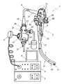
図1に示すように、電子内視鏡システム1は、撮像手段を備えた電子内視鏡2と、電子内視鏡2に着脱自在に接続されて電子内視鏡2に設けられたライトガイドに照明光を供給する光源装置3と、電子内視鏡2と接続ケーブル4を介して接続されて電子内視鏡2の撮像手段を制御すると共に撮像手段から得られた信号を処理するビデオプロセッサ5と、ビデオプロセッサ5から出力される被写体像に対応する映像を表示するモニタ6から構成されている。このモニタ6の走査方向は、垂直方向は上から下へ、水平方向は左から右へ走査されるものである。
【0013】
電子内視鏡2は、可撓性を有する細長の挿入部7と、挿入部7の基端側に接続された操作部8と、操作部8の側部から延出した可撓性を有する連結コード9と、連結コード9の端部に設けられた前記光源装置3と着脱自在に接続されるコネクタ部10と、コネクタ部10の側部に設けられた前記ビデオプロセッサ5と接続された前記接続ケーブル4が着脱自在に接続可能な電気コネクタ部11とを有している。
【0014】
電気コネクタ部11には電子内視鏡2の内部と外部とを連通する図示しない通気部が設けられている。
【0015】
挿入部7と操作部8の接続部には、接続部の急激な曲がりを防止する弾性部材を有する挿入部側折れ止め部材12が設けられており、操作部8と連結コード9の接続部には同様の操作部側折れ止め部材13、連結コード9とコネクタ部10の接続部には同様のコネクタ部側折れ止め部材14が設けられている。
【0016】
挿入部7は、可撓性を有する柔軟な可撓管部15と、可撓管部15の先端側に設けられ操作部8の操作により湾曲可能な湾曲部16と、図2に示す観察光学系をなす撮像装置18、照明光学系19などが配設された先端部17から構成されている。
【0017】
図1に示すように、コネクタ部10には光源装置3に内蔵された図示しない気体供給源と着脱自在に接続される気体供給口金21と、液体供給源である送水タンク22と着脱自在に接続される送水タンク加圧口金23及び液体供給口金24とが設けられている。又、前記吸引口より吸引を行うための図示しない吸引源と接続される吸引口金25が設けられている。
【0018】
又、高周波処置等を行った際に内視鏡に高周波漏れ電流が発生した場合に漏れ電流を高周波処置装置に帰還させるためのアース端子口金27が設けられている。
【0019】
操作部8には送気操作、送水操作を操作する送気送水操作ボタン28と吸引操作を操作するための吸引操作ボタン29と、前記湾曲部の湾曲操作を行うための湾曲操作ノブ30と、前記ビデオプロセッサ5を遠隔操作する複数のリモートスイッチ31、前記処置具チャンネルと連通した開口である処置具挿入口32が設けられている。
【0020】
また、電子内視鏡2の電気コネクタ部11には電気コネクタ部11を液密にシールするための図示しない防水キャップが着脱自在に接続可能である。
【0021】
図2に示すように、複数の対物レンズ33は第1、2対物レンズ枠34、35の中にフレア防止用の光学絞り65及び所定の対物レンズ間距離を保つための間隔管66を介在した状態で配設される。複数の対物レンズ33の最後端レンズには、紫外線硬化型接着剤等により接合された固体撮像装置37が、複数の対物レンズ33の結像位置に配置されている。
【0022】
固体撮像装置37は、図3に示すように、カバーガラス38と、固体撮像素子39と、外部リード40から構成されており、カバーガラス38は固体撮像素子39の受光部20を覆うように紫外線硬化型接着剤にて接着固定されている。この固体撮像素子39の側面(左右方向)に配置される外部リード40は、ポリイミドテープ41(図2参照)上に銅箔により配線が形成されたフレキシブル基板であり、ポリイミドテープ41より延出するインナーリード42は受光部20の左右に形成されたボンディングパッド69に金等のボールバンプを介して接続されている(ボールボンディング)。そして、この固体撮像装置37の走査方向は、垂直方向は下から上へ、水平方向は左から右へと走査される。
【0023】
図2に戻り、この外部リード40のアウターリード43は、固体撮像素子39の後方に配置された固体撮像装置37の短辺と長辺の配置方向と、図4に示すモニタ6の表示画像上下左右方向と、先端部17の上下左右方向とを関連付けするための表示方向選択手段である複数の電子部品44が実装された回路基板45の側面に形成されたサイドスルーホールに半田等により接続されている。そして、複数の信号線46は、アウターリード43が接続される面とは異なる側面に形成されたサイドスルーホールヘと半田等により接続されている。
【0024】
ここで、この表示方向選択手段は、図5に示すように、固体撮像装置37の配置方向と、先端部17の湾曲動作方向と、モニター6上での画像表示方向との関連付けをするものであり、複数の電子部品44を用いた論理回路にて構成されている。
【0025】
なお、図5では4組の関連付けを示したが、当然、それに限定されるものではなく更に複数個の組合せも可能である。
【0026】
複数の信号線46は、図6に示すように、ケブラー等の繊維からなる介在36を中心として寄り束ねられ、その外周にはPTFE等からなるテープ47が螺旋状に被覆されている。そして、その外周には、すずめっき銅合金製のシールド導体48が形成された上にPFAからなる絶縁体49が被覆されることにより信号ケーブル50が形成されている。尚、信号線46の周囲には、信号ケーブル50基端側からの湿気進入を防止するために接着剤71が少なくとも図2中のLの範囲に渡り充填されている。もちろん、全長に渡って充填されても良い。この接着剤71は先端側よりディスペンサにより注入したり、基端側より吸引して充填しても良い。
【0027】
図2に戻り、この信号ケーブル50の外周には、電子内視鏡2の内蔵物からの干渉による破損を防止するためのケーブル保護51が絹糸52により抜けないように結束されている。
【0028】
そして、この固体撮像装置37と回路基板45と信号線46とが接続された後、前記電装構成部周囲には湿気等が進入しないようにエポキシ樹脂よりなる封止樹脂53がシールド枠54内に充填され、このシールド枠54は熱収縮チユーブ55により被覆されている。
【0029】
照明光学系19は、照明レンズ枠56内に配置された照明レンズ57と、この照明レンズ57に当接するライトガイドファイバ58を固定した固定筒59と、固定筒59より後端側のライトガイドファイバ58を被覆するシリコン等からなる被覆チューブ60により構成されている。
【0030】
そして、この前記撮像装置18と照明光学系19は、先端部17を構成する絶縁カバー61と先端硬性部材62に形成した撮像装置取付け孔63、照明光学系取付け孔64に嵌装され接着剤にて固定されている。
【0031】
また、先端部17には送気操作、送水操作によって観察光学系の外表面の光学部材に向けて洗滌液体や気体を先端部に導くための送気送水チャンネルを介して噴出するための図示しない送気送水ノズルと、挿入部7に配設された処置具を挿通したり体腔内の液体を吸引するための処置具チャンネルの先端側開口である吸引口が設けられている。
【0032】
図7は図2に示す先端部17のA−A線縦断面図であり、前述したように先端部17には外形が長方形状の固体撮像装置37を配設する撮像装置18と、円状の照明光学系19、送気送水チャンネル67、処置具チャンネル68が配設されている。
【0033】
このように本実施の形態では、図7に示すように機械的に90°時計周り方向に回転させて配置した固体撮像装置37の取り込み画像を、図8に示すように撮像装置18内に設けた複数の電子部品44より構成される表示方向選択手段44aにて電気的に反時計方向へ90°回転させることで、モニタ6の表示画像上下左右方向と、先端部17の上下左右方向とを一致させることができるので電子内視鏡を操作しやすくなる。
【0034】
また、図7に示すように、固体撮像装置37を90°回転させて縦置きできたため、回転させられない破線で示す撮像装置を配置するよりも先端部17を細径化することができるとともに、修理等で撮像装置を交換しても、その表示方向選択手段44aが撮像装置18内にあるので、確実に正常な画像をモニタ表示することができる。
【0035】
また、撮像装置18内に表示方向選択手段44aを設けることで、1つの固体撮像装置37を使用する撮像装置18にて、複数の電子内視鏡の先端部を細経化することができる。
【0036】
なお、本実施例では90°回転させた場合を説明したが、固体撮像素子の配置方向はこの限りではなく、個々の電子内視鏡が有する内蔵物に応じて、任意の角度にて配置可能である。
【0037】
なお、表示方向選択手段44aを、例えば先端部湾曲動作方向に対する固体撮像装置37の配置方向に基づいて対物光学系より得られる像をどのように反転/変換するかを指示するための表示方向指示手段201と、その指示に応じて、先端部17の湾曲動作方向とモニタ6上での表示画像方向とを一致させるための固体撮像装置37での取り込み画像を変換処理する映像処理回路からなる表示方向変換手段202とに分離することにより、それぞれを配置するスペースを小型化することができる。具体的には図9に示すように、表示方向指示手段201を撮像装置18に配置し、表示方向変換手段202をビデオプロセッサ5内に配置することで撮像装置18を表示方向選択手段にて使用していたときの撮像装置における電子部品44の個数、大きさを削減できるので撮像装置18を小型化することができる。よって、撮像装置18を配設する先端部17を細径化することができる。
【0038】
なお、回路基板45の変形例として、図10に示すように、4隅にサイドスルーホール74を形成してもよく、これにより、接続電極であるサイドスルーホール数を減らすことなく、破線で示す回路基板45を小型化することができるので、撮像装置18を小型化することができる。
【0039】
また、電子内視鏡システム1では、図11のように固体撮像装置72に取り込んだ画像が受光部上でA程度ブレた場合、固体撮像装置72の受光部内ブレ補正処理領域75を用いて、A程度ずらした受光画像をビデオプロセッサ5へ伝送し、モニタ表示することができる。また、ビデオプロセッサ5にブレ補正領域75の画像データを用いてブレ補正処理するための図示しない映像処理回路を設けて、モニタ表示しても良い。
【0040】
これにより、先端部が小刻みに揺れ動いたとしてもブレない観察画像を得ることができる。特に、体内の微少な拍動により観察画像にブレが発生しやすい拡大観察時には有効であり、拡大観察への切替と連動でブレ補正を行うと効果的である。
【0041】
図12に示す固体撮像装置76は、固体撮像素子77の裏面にIC78等の電子部品が実装された回路基板79が取付けられたものである。このIC78は、予め接続基板80上にフリップチップ実装された後、接続基板80の側面に形成されたサイドスルーホールを用いて、回路基板79と半田等で接続されている。そして、この固体撮像装置76の周辺は封止樹脂81にて覆われ、熱収縮チューブ82にて被覆され、その外周には固体撮像装置76及びIC78の発熱を先端硬性部材62に放熱するための放熱枠83が取付けられている。この放熱枠83の後端側は末広がりに開口しており、その開口部84は先端硬性部材62内に嵌装される時に、先端硬性部材62と接触し、接触部は接着剤85にて先端硬性部材62に固定される。
【0042】
これにより、固体撮像装置76やIC78が発生する熱を、接触部より先端硬性部材62へと放熱することができるので、固体撮像装置76やIC78の劣化を防止することができる。
【0043】
図13は回路基板79の上面図である。この回路基板79の基端側には信号線46を取付けるための複数の取付けランド86が形成されており、取付けランド86の基端側には取付けランド86をマスキングする、例えば、絶縁テープ等からなるマスキング部材87が取付けられている。
【0044】
これにより、信号線46は初期組立時は取り付けランド86の前方に取り付け、信号線46が断線等により交換作業が発生した場合は、マスキング部材87を取り除き、図15に示すように基端側の取付けランド86に信号線46を接続することができるので、回路基板の再利用が可能となる。
【0045】
また、図15に示すように回路基板88の上下面に取り付けランド89を形成し、双方は基板に形成されたスルホール90にて接続されている。よって、信号線46等が断線し、交換作業が発生した場合は、もう一方の取付けランド89に信号線46を接続すれば良く、回路基板88を再利用することができる。
【0046】
尚、セラミック等により形成される硬質の回路基板88に限定されるものではなく、図16に示すように、ポリイミドテープ108を挟むように導電部109が両面に形成されたフレキシブル回路基板91にも同様に適用することができる。
【0047】
図17に示す固体撮像装置92の回路基板93の底面にはGND部117が形成されており、そのGND部117には放熱枠94の一部が面接触されるように回路基板93に取付けられている。
【0048】
これにより、固体撮像装置92の発熱を放熱枠94へと放熱することができる。また、GND部を広く取ることができるので外部ノイズ等に対して耐性の強い撮像装置となる。
【0049】
図18の固体撮像装置95は、固体撮像素子96下端に、予め電子部品97等が実装されたフレキシブル回路基板98先端より延出するインナーリード99が屈曲接続されたものである。このフレキシブル回路基板98は、電子部品97を取り付けるランドや配線等を形成する導電部100が絶縁性のポリイミド101を挟んで両面に形成されている。
【0050】
この時、フレキシブル回路基板98の導電部100を厚く(t1、t3>t2)形成することで、固体撮像装置95の熱容量を大きくすることができるので熱に対する耐性が高い固体撮像装置を構成することができる。
【0051】
図19の固体撮像装置102は、フレキシブル回路基板103の後端側を屈曲させて先端硬性部材62に取付けると共に、固体撮像装置102全体を接着剤105にて封止している。
【0052】
これにより、固体撮像装置の発熱を先端硬性部材62へと放熱することができるので、固体撮像装置の劣化を防止することができる。
【0053】
図20の固体撮像装置106は、固体撮像素子107裏面に先端硬性部材62と接続される放熱部材108が取付けられている。
【0054】
これにより、固体撮像装置106の発熱を先端硬性部材62へと放熱することができるので、固体撮像装置の劣化を防止することができる。また、固体撮像装置106を先端硬性部材62内へと嵌装する際に、放熱部剤108を保持しながら取付作業が行えるので組み立て性が向上する。
【0055】
図21の固体撮像装置110のフレキシブル回路基板111裏面には、接続電極が形成されており、ケーブル50が接続された接続電極113を有する接続基板112とフレキシブル回路基板111とを導電性接着剤にて接続することで接続電極同士を接続することが可能となる。
【0056】
これにより、組立性が向上すると共に、信号線46が断線した時でも、フレキシブル回路基板114に新しい信号ケーブル50が接続された接続基板112を取り付けることができるので、固体撮像装置110のフレキシブル回路基板111を破損することなく修理が行える。
【0057】
図22に示す固体撮像装置114は、複数の、例えば4つの出力ライン118を有するものであり、その出力ラインは受光部片側の側方を通って固体撮像装置114上部側へ形成されたボンディングパッド115へと導かれ、フレキシブル回路基板116へと接続されている。
【0058】
これにより、固体撮像装置の外形中心と受光部中心とを近づけることができるので、先端部を小型化することができる。
【0059】
また、フレキシブル回路基板116を固体撮像装置114の上側に配置することで、受光部の中心位置を固体撮像装置114の上側端部より遠ざけることができるので、対物レンズ部を固体撮像装置114及び撮像装置外形の下側に配置することができるので、対物レンズ部上側の空いたスペースに他の内蔵物を配置することができる。よって、先端部を細径化することができる。
【0060】
[付記]
(付記項1) モニタ出画範囲と同数、もしくはそれ以上の画素数を有する固体撮像装置を搭載した撮像装置を先端部に配置した電子内視鏡と、前記撮像装置からの撮像信号を信号処理するビデオプロセッサとより構成される電子内視鏡システムにおいて、
前記ビデオプロセッサの映像処理により形成される電子マスクにより、内視鏡観察画像表示範囲を表示手段の全表示範囲よりも小さく形成し、前記電気マスクにて前記表示手段に表示されない画素を手ぶれ防止のために用いる
ことを特徴とする電子内視鏡システム。
【0061】
(付記項2) 拡大観察時に前記電気マスクにて前記表示手段に表示されない画素を手ぶれ防止のために用いる
ことを特徴とする付記項1に記載の電子内視鏡システム。
【0062】
(付記項3) 固体撮像装置と、回路基板と、信号ケーブルとが電気的に接続された撮像装置において、
前記固体撮像装置と接続される前記回路基板の端部にスルーホールを形成した
ことを特徴とする撮像装置。
【0063】
(付記項4) 固体撮像装置と、回路基板と、信号ケーブルとが電気的に接続された撮像装置において、
前記信号ケープルの前記固体撮像装置側側端部に接着剤充填範囲を形成した
ことを特徴とする撮像装置。
【0064】
(付記項5) 固体撮像装置と、回路基板と、信号ケーブルとが電気的に接続された撮像装置において、
前記回路基板に形成した複数の信号ケーブル接続部の内、前記信号ケーブル接続部の一部を非導電材のマスキング材にて覆った
ことを特徴とする撮像装置。
【0065】
(付記項6) 固体撮像装置と、回路基板と、信号ケーブルとが電気的に接続された撮像装置において、
前記信号ケーブルを接続する前記信号ケーブル接続部を前記回路基板の表裏面に設け、それぞれをスルーホールにて接続した
ことを特徴とする撮像装置。
【0066】
(付記項7) 補強枠内に配置される固体撮像装置と、回路基板と、信号ケーブルとが電気的に接続された撮像装置において、
補強枠後端側の一部に末広がり状に形成された切り欠き部が先端部と接触している
ことを特徴とする撮像装置。
【0067】
(付記項8) 補強枠内に配置される固体撮像装置と、回路基板と、信号ケーブルとが電気的に接続された撮像装置において、
前記回路基板に大きめのGND部を形成し、前記GND部と前記補強枠とを導通させた
ことを特徴とする撮像装置。
【0068】
(付記項9) 補強枠内に配置される固体撮像装置と、固体撮像装置の周辺に放熱部材を配置した撮像装置において、
前記放熱部材を前記補強枠へ接続した
ことを特徴とする撮像装置。
【0069】
(付記項10) フレキシブル回路基板を用いた固体撮像装置を配置する撮像装置において、
前記フレキシブル回路基板に、信号ケーブルが接続された接続用フレキシブル基板が接続された
ことを特徴とする撮像装置。
【0070】
(付記項11) フレキシブル回路基板を用いた固体撮像装置を配置する撮像装置において、
前記フレキシブル回路基板の後方側に形成したGND部を先端部に接続した
ことを特徴とする撮像装置。
【0071】
(付記項12) フレキシブル回路基板を用いた固体撮像装置を配置する撮像装置において、
前記フレキシブル回路基板の導電部層の厚みを基材の樹脂層よりも厚く形成した
ことを特徴とする撮像装置。
【0072】
(付記項13) フレキシブル回路基板を用いた固体撮像装置を配置する撮像装置において、
前記フレキシブル回路基板を前記固体撮像装置上側に接続配置し、前記フレキシブル回路基板が後方へ延出すると共に、フレーム転送された電気信号が受光部下方にある水平転送領域より、受光部のOB部領域の側方より、上側へ配線される
ことを特徴とする撮像装置。
【0073】
【発明の効果】
以上説明したように本発明によれば、固体撮像素子の配置方向によらず、モニタの表示画像上下左右方向と内視鏡先端部の上下左右方向とを一致させることができるという効果がある。
【図面の簡単な説明】
【図1】 本発明の一実施の形態に係る電子内視鏡システムの構成を示す構成図
【図2】 図1の電子内視鏡の先端部の長手軸方向の断面を示す断面図
【図3】 図2の固体撮像装置の構成を示す構成図
【図4】 図1のモニタの表示画像上下左右方向を示す図
【図5】 図3の固体撮像装置の配置方向と電子内視鏡の先端部の湾曲動作方向及びモニタの表示方向の関連を示す図
【図6】 図2の信号線の基端側の構成を示す図
【図7】 図2のA−A線断面を示す断面図
【図8】 図2の複数の電子部品により構成される表示方向選択手段の電子内視鏡システム上の配置を示す図
【図9】 図2の複数の電子部品により構成される表示方向選択手段の電子内視鏡システム上の配置の変形例を示す図
【図10】 図2の回路基板の第1の変形例を示す図
【図11】 図1のビデオプロセッサにブレ補正処理機能を備えた際の作用を説明する図
【図12】 図2の固体撮像装置の第1の変形例を示す図
【図13】 図2の回路基板の第2の変形例を示す第1の図
【図14】 図2の回路基板の第2の変形例を示す第2の図
【図15】 図2の回路基板の第3の変形例を示す図
【図16】 図2の回路基板の第4の変形例を示す図
【図17】 図2の回路基板の第5の変形例を示す図
【図18】 図2の固体撮像装置の第2の変形例を示す図
【図19】 図2の固体撮像装置の第3の変形例を示す図
【図20】 図2の固体撮像装置の第4の変形例を示す図
【図21】 図2の固体撮像装置の第5の変形例を示す図
【図22】 図2の固体撮像装置の第6の変形例を示す図
【図23】 被写体の上下左右とモニタ表示上の上下左右との関係を説明する図
【符号の説明】
1…電子内視鏡システム
2…電子内視鏡
3…光源装置
5…ビデオプロセッサ
6…モニタ
37…固体撮像装置
38…カバーガラス
39…固体撮像素子
40…外部リード
44…電子部品
44a…表示方向選択手段
45…回路基板
46…信号線[0001]
BACKGROUND OF THE INVENTION
The present invention relates to an electronic endoscope system, and more particularly to an electronic endoscope system characterized by a conversion portion of an image captured by an imaging apparatus.
[0002]
[Prior art]
As shown in Japanese Examined Patent Publication No. 3-37405, an observation image of an electronic endoscope is obtained by displaying a video signal obtained from a solid-state imaging device arranged at the tip on a monitor TV screen via a control device. Yes. Since each electronic endoscope has a different objective optical system, it is necessary to invert the image depending on the type of the objective optical system, and the image inversion setup means is provided in the connector device of each electronic endoscope. The technology to provide is shown.
[0003]
For example, the scanning direction of the NTSC monitor is unified from left to right in the horizontal direction and from top to bottom in the vertical direction. Therefore, as shown in FIG. 23, when observing a subject using an optical system, in order to align the top, bottom, left, and right of the subject and the top, bottom, left, and right of the monitor display, the horizontal direction of the scanning direction of the solid-state imaging device is from left to right. The vertical direction is from bottom to top.
[0004]
The outer shape of the solid-state imaging device is rectangular according to the number of pixels that each individual solid-state imaging device has, the size of the light receiving unit, the mounting direction of the lead terminals, and the like.
[0005]
[Problems to be solved by the invention]
Conventionally, since the image inverting means is provided in the connector device, a normal image cannot always be displayed on the monitor when the imaging device or the connector device is replaced for repair or the like.
[0006]
In addition, when a solid-state imaging device having a rectangular outer shape is mounted on the distal end portion of an electronic endoscope, the distal end portion outer diameter may have to be increased depending on the arrangement direction of the short side and the long side. Therefore, if the solid-state imaging device is rotated 90 ° in order to reduce the outer diameter of the distal end, the display image on the monitor is also rotated 90 °, and the UP direction of the endoscope distal end and the UP direction of the monitor display image Did not match, making it difficult to operate the endoscope. That is, a normal image may not be displayed on the monitor by changing not only the objective optical system but also the arrangement of the solid-state imaging device.
[0007]
In addition, there is a means to change the outer shape of the solid-state image pickup device and a means to change the scanning direction of the solid-state image pickup device in order to reduce the size of the endoscope distal end described above, but a new solid-state image pickup device has been developed individually. Doing so is very inefficient and increases the cost of the endoscope.
[0008]
The present invention has been made in view of the above circumstances, and an electronic device capable of matching the vertical and horizontal directions of the display image of the monitor with the vertical and horizontal directions of the distal end portion of the endoscope irrespective of the arrangement direction of the solid-state imaging device. An object is to provide an endoscope system.
[0009]
[Means for Solving the Problems]
An electronic endoscope system according to the present invention includes an objective optical system disposed at a distal end portion of an electronic endoscope, and a solid state disposed at a predetermined position at the distal end portion as an imaging position of the objective optical system. An electronic endoscope including an imaging device having at least an imaging device, and a video that is connected to the electronic endoscope via a connector device and processes an imaging signal from the imaging device and displays an endoscope image on a display means In an electronic endoscope system comprising a processor and a light source device that supplies illumination light to the electronic endoscope, the electronic endoscope system is disposed in the imaging device Direction indication means When the vertical scanning direction of the solid-state imaging device is the vertical direction of the solid-state imaging device and the horizontal scanning direction is the horizontal direction of the solid-state imaging device, the solid-state imaging device is disposed at a predetermined position at the tip portion. When the vertical and horizontal arrangement directions of the solid-state imaging device and the predetermined bending operation direction at the tip of the electronic endoscope are defined as the vertical and horizontal directions of the tip In Up / down / left / right bending motion direction of the tip Direction indicating means for outputting positional relationship information indicating a relative positional relationship between the tip and the solid-state imaging device based on And said Output from direction indicator The relative direction of the vertical and horizontal arrangement directions of the solid-state imaging device and the vertical and horizontal bending operation directions of the tip portion The positional relationship information indicating the positional relationship The display direction for converting the display direction of the endoscopic image so that the vertical and horizontal directions related to the bending operation direction of the distal end portion coincide with the vertical and horizontal directions of the image display direction on the display screen of the display means Conversion means.
[0010]
DETAILED DESCRIPTION OF THE INVENTION
Embodiments of the present invention will be described below with reference to the drawings.
[0011]
1 to 22 relate to an embodiment of the present invention, FIG. 1 is a block diagram showing the configuration of an electronic endoscope system, and FIG. 2 is a cross section in the longitudinal axis direction of the distal end portion of the electronic endoscope of FIG. 3 is a block diagram showing the configuration of the solid-state imaging device of FIG. 2, FIG. 4 is a diagram showing the vertical and horizontal directions of the display image of the monitor of FIG. 1, and FIG. 5 is the arrangement direction of the solid-state imaging device of FIG. FIG. 6 is a diagram showing the configuration of the proximal end side of the signal line in FIG. 2, and FIG. 7 is an AA diagram in FIG. 8 is a cross-sectional view showing a line cross section, FIG. 8 is a view showing an arrangement on the electronic endoscope system of a display direction selecting means constituted by a plurality of electronic components in FIG. 2, and FIG. 9 is constituted by a plurality of electronic components in FIG. FIG. 10 is a diagram showing a modification of the arrangement of the display direction selection means on the electronic endoscope system, and FIG. 10 is a first modification of the circuit board of FIG. Diagram showing, 11 to the video processor of FIG. 1 Blur FIG. 12 is a diagram illustrating an operation when the correction processing function is provided, FIG. 12 is a diagram illustrating a first modification of the solid-state imaging device in FIG. 2, and FIG. 13 is a second modification illustrating the circuit board in FIG. 14 is a second diagram showing a second modification of the circuit board of FIG. 2, FIG. 15 is a diagram showing a third modification of the circuit board of FIG. 2, and FIG. 16 is a circuit of FIG. FIG. 17 is a diagram showing a fourth modification of the substrate, FIG. 17 is a diagram showing a fifth modification of the circuit board in FIG. 2, FIG. 18 is a diagram showing a second modification of the solid-state imaging device in FIG. Is a diagram showing a third modification of the solid-state imaging device of FIG. 2, FIG. 20 is a diagram showing a fourth modification of the solid-state imaging device of FIG. 2, and FIG. 21 is a fifth modification of the solid-state imaging device of FIG. FIG. 22 is a diagram illustrating an example, and FIG. 22 is a diagram illustrating a sixth modification of the solid-state imaging device of FIG.
[0012]
As shown in FIG. 1, an
[0013]
The
[0014]
The
[0015]
The connecting portion between the insertion portion 7 and the
[0016]
The insertion portion 7 includes a flexible
[0017]
As shown in FIG. 1, the
[0018]
In addition, when a high frequency leakage current is generated in the endoscope when a high frequency treatment or the like is performed, an
[0019]
The
[0020]
In addition, a waterproof cap (not shown) for sealing the
[0021]
As shown in FIG. 2, the plurality of
[0022]
As shown in FIG. 3, the solid-
[0023]
Returning to FIG. 2, the outer leads 43 of the external leads 40 are arranged in the arrangement direction of the short side and the long side of the solid-
[0024]
Here, as shown in FIG. 5, the display direction selection means associates the arrangement direction of the solid-
[0025]
In FIG. 5, four sets of associations are shown, but the present invention is not limited to this, and a plurality of combinations are possible.
[0026]
As shown in FIG. 6, the plurality of
[0027]
Returning to FIG. 2, a
[0028]
After the solid-
[0029]
The illumination
[0030]
The
[0031]
In addition, the
[0032]
FIG. 7 is a vertical cross-sectional view of the
[0033]
Thus, in this embodiment, the figure 7 As shown in 9 mechanically A captured image of the solid-
[0034]
In addition, as shown in FIG. 90 ° Since it can be rotated and placed vertically, the
[0035]
In addition, by providing the display direction selection means 44a in the
[0036]
In the present embodiment, the case of rotating by 90 ° has been described. However, the arrangement direction of the solid-state imaging device is not limited to this, and can be arranged at an arbitrary angle according to the built-in objects of each electronic endoscope. It is.
[0037]
For example, the display
[0038]
As a modified example of the
[0039]
Further, in the
[0040]
As a result, even if the tip swings in small increments Blur No observation image can be obtained. This is particularly effective during magnified observation, where the observed image is likely to be blurred due to minute pulsations in the body. Blur It is effective to make corrections.
[0041]
A solid-state imaging device 76 shown in FIG. 12 has a
[0042]
Thereby, the heat generated by the solid-state imaging device 76 and the
[0043]
FIG. 13 is a top view of the
[0044]
As a result, the
[0045]
Further, as shown in FIG. 15, mounting
[0046]
Note that the
[0047]
A
[0048]
Thereby, the heat generated by the solid-state imaging device 92 can be radiated to the
[0049]
The solid-
[0050]
At this time, by forming the
[0051]
In the solid-
[0052]
Thereby, since the heat generated by the solid-state imaging device can be radiated to the distal end
[0053]
In the solid-
[0054]
Thereby, since the heat generated by the solid-
[0055]
A connection electrode is formed on the back surface of the
[0056]
As a result, the assemblability is improved, and even when the
[0057]
The solid-
[0058]
As a result, the center of the outer shape of the solid-state imaging device and the center of the light receiving unit can be brought close to each other, so that the tip can be reduced in size.
[0059]
In addition, by disposing the
[0060]
[Appendix]
(Additional Item 1) An electronic endoscope in which an imaging device equipped with a solid-state imaging device having the same number of pixels as or more than the monitor output range is disposed at the tip, and signal processing of an imaging signal from the imaging device In an electronic endoscope system comprising a video processor
The electronic mask formed by the video processing of the video processor forms an endoscopic observation image display range smaller than the entire display range of the display means, and prevents pixels that are not displayed on the display means by the electric mask from shaking. Use for
An electronic endoscope system characterized by that.
[0061]
(Additional Item 2) Pixels that are not displayed on the display means by the electric mask during magnified observation are used to prevent camera shake.
Item 3. The electronic endoscope system according to
[0062]
(Additional Item 3) In an imaging device in which a solid-state imaging device, a circuit board, and a signal cable are electrically connected,
A through hole was formed at an end of the circuit board connected to the solid-state imaging device.
An imaging apparatus characterized by that.
[0063]
(Additional Item 4) In an imaging device in which a solid-state imaging device, a circuit board, and a signal cable are electrically connected,
An adhesive filling range was formed at the solid-state imaging device side end of the signal cable.
An imaging apparatus characterized by that.
[0064]
(Additional Item 5) In an imaging device in which a solid-state imaging device, a circuit board, and a signal cable are electrically connected,
Of the plurality of signal cable connection portions formed on the circuit board, a part of the signal cable connection portion is covered with a non-conductive masking material.
An imaging apparatus characterized by that.
[0065]
(Additional Item 6) In an imaging device in which a solid-state imaging device, a circuit board, and a signal cable are electrically connected,
The signal cable connecting portion for connecting the signal cable is provided on the front and back surfaces of the circuit board, and each is connected through a through hole.
An imaging apparatus characterized by that.
[0066]
(Additional Item 7) In an imaging device in which a solid-state imaging device, a circuit board, and a signal cable arranged in a reinforcing frame are electrically connected,
A notch formed in a divergent shape at the rear end of the reinforcing frame is in contact with the tip
An imaging apparatus characterized by that.
[0067]
(Additional Item 8) In an imaging device in which a solid-state imaging device, a circuit board, and a signal cable are disposed in a reinforcing frame,
A large GND portion was formed on the circuit board, and the GND portion and the reinforcing frame were made conductive.
An imaging apparatus characterized by that.
[0068]
(Additional Item 9) In the solid-state imaging device arranged in the reinforcing frame and the imaging device in which the heat dissipation member is arranged around the solid-state imaging device,
The heat dissipation member was connected to the reinforcement frame
An imaging apparatus characterized by that.
[0069]
(Additional Item 10) In an imaging device in which a solid-state imaging device using a flexible circuit board is arranged,
A flexible board for connection to which a signal cable is connected is connected to the flexible circuit board.
An imaging apparatus characterized by that.
[0070]
(Additional Item 11) In an imaging device in which a solid-state imaging device using a flexible circuit board is arranged,
The GND part formed on the rear side of the flexible circuit board was connected to the tip part.
An imaging apparatus characterized by that.
[0071]
(Additional Item 12) In an imaging device in which a solid-state imaging device using a flexible circuit board is arranged,
The thickness of the conductive part layer of the flexible circuit board was made thicker than the resin layer of the base material
An imaging apparatus characterized by that.
[0072]
(Additional Item 13) In an imaging device in which a solid-state imaging device using a flexible circuit board is arranged,
The flexible circuit board is connected to the upper side of the solid-state imaging device, the flexible circuit board extends rearward, and the frame-transferred electrical signal is transmitted from the horizontal transfer area below the light receiving section to the OB section area of the light receiving section. Wiring from the side to the upper side
An imaging apparatus characterized by that.
[0073]
【The invention's effect】
As described above, according to the present invention, there is an effect that the vertical and horizontal directions of the display image of the monitor can be matched with the vertical and horizontal directions of the distal end portion of the endoscope regardless of the arrangement direction of the solid-state imaging device.
[Brief description of the drawings]
FIG. 1 is a configuration diagram showing a configuration of an electronic endoscope system according to an embodiment of the present invention.
2 is a cross-sectional view showing a cross section in a longitudinal axis direction of a distal end portion of the electronic endoscope of FIG. 1;
3 is a configuration diagram showing the configuration of the solid-state imaging device of FIG. 2;
4 is a diagram showing the display image on the monitor shown in FIG.
5 is a diagram showing the relationship between the arrangement direction of the solid-state imaging device of FIG. 3, the bending operation direction of the distal end portion of the electronic endoscope, and the display direction of the monitor.
6 is a diagram showing a configuration of a base end side of the signal line in FIG. 2;
7 is a cross-sectional view showing a cross section taken along the line AA in FIG.
FIG. 8 is a diagram showing an arrangement on the electronic endoscope system of display direction selection means constituted by a plurality of electronic components in FIG. 2;
FIG. 9 is a view showing a modification of the arrangement on the electronic endoscope system of the display direction selection means constituted by a plurality of electronic components in FIG. 2;
10 is a diagram showing a first modification of the circuit board of FIG. 2;
FIG. 11 shows a video processor of FIG. Blur The figure explaining the effect at the time of having a correction processing function
FIG. 12 is a diagram showing a first modification of the solid-state imaging device of FIG.
FIG. 13 is a first diagram showing a second modification of the circuit board of FIG. 2;
14 is a second diagram showing a second modification of the circuit board of FIG. 2. FIG.
FIG. 15 is a diagram showing a third modification of the circuit board in FIG. 2;
FIG. 16 is a diagram showing a fourth modification of the circuit board in FIG. 2;
FIG. 17 is a diagram showing a fifth modification of the circuit board in FIG. 2;
FIG. 18 is a diagram showing a second modification of the solid-state imaging device of FIG.
FIG. 19 is a diagram showing a third modification of the solid-state imaging device of FIG.
20 is a diagram illustrating a fourth modification of the solid-state imaging device in FIG. 2;
FIG. 21 is a diagram illustrating a fifth modification of the solid-state imaging device in FIG. 2;
FIG. 22 is a diagram showing a sixth modification of the solid-state imaging device in FIG. 2;
FIG. 23 is a diagram for explaining the relationship between the vertical and horizontal directions of the subject and the vertical and horizontal directions on the monitor display;
[Explanation of symbols]
1 ... Electronic endoscope system
2 ... Electronic endoscope
3. Light source device
5 ... Video processor
6 ... Monitor
37. Solid-state imaging device
38 ... cover Glass
39 ... Solid-state image sensor
40 ... External lead
44 ... Electronic components
44a ... Display direction selection means
45 ... Circuit board
46 ... Signal line
Claims (2)
前記電子内視鏡とコネクタ装置を介して接続され前記撮像装置からの撮像信号を信号処理し表示手段に内視鏡画像を表示させるビデオプロセッサと、
前記電子内視鏡に照明光を供給する光源装置とを備えた電子内視鏡システムにおいて、
前記撮像装置に配設された方向指示手段であって、前記固体撮像装置の垂直走査方向を当該固体撮像装置における上下方向とし、水平走査方向を当該固体撮像装置における左右方向とした場合の、前記先端部において予め決められた位置に配置された当該固体撮像装置の上下左右の配置方向と、前記電子内視鏡の先端部における所定の湾曲動作方向を当該先端部の上下左右方向と規定した場合において、当該先端部の上下左右の湾曲動作方向に基づく当該先端部と前記固体撮像装置の相対的な位置関係を示す位置関係情報を出力する方向指示手段と、
前記方向指示手段から出力された、前記固体撮像装置の上下左右の配置方向と、前記先端部の上下左右の湾曲動作方向との相対的な位置関係を示す前記位置関係情報に基づいて、前記先端部の湾曲動作方向に係る上下左右方向と、前記表示手段の表示画面における画像表示方向の上下左右方向とを一致させるよう前記内視鏡画像の表示方向を変換する表示方向変換手段と、
を具備したことを特徴とする電子内視鏡システム。An electronic device comprising an imaging device having at least a solid-state imaging device arranged at a position determined in advance at an imaging position of the objective optical system, wherein an objective optical system is arranged at a distal end portion of the electronic endoscope An endoscope,
A video processor that is connected to the electronic endoscope via a connector device and that performs signal processing on an imaging signal from the imaging device and displays an endoscopic image on a display unit;
In an electronic endoscope system including a light source device that supplies illumination light to the electronic endoscope,
Direction indicating means disposed in the imaging device, wherein the vertical scanning direction of the solid-state imaging device is the vertical direction in the solid-state imaging device, and the horizontal scanning direction is the horizontal direction in the solid-state imaging device. When the vertical and horizontal arrangement directions of the solid-state imaging device arranged at a predetermined position at the distal end and the predetermined bending operation direction at the distal end of the electronic endoscope are defined as the vertical and horizontal directions of the distal end in a direction instruction means for outputting a positional relationship information indicating a relative positional relationship of the with the tip based on the bending operation directions of up, down, left and right of the front end portion the solid-state imaging device,
Based on the positional relationship information indicating the relative positional relationship between the up / down / left / right arrangement directions of the solid-state imaging device and the up / down / left / right bending operation directions of the distal end portion, which is output from the direction instruction means. Display direction conversion means for converting the display direction of the endoscopic image so as to match the vertical and horizontal directions related to the bending operation direction of the unit and the vertical and horizontal directions of the image display direction on the display screen of the display means;
An electronic endoscope system comprising:
Priority Applications (1)
| Application Number | Priority Date | Filing Date | Title |
|---|---|---|---|
| JP2000312508A JP5063834B2 (en) | 2000-10-12 | 2000-10-12 | Electronic endoscope system |
Applications Claiming Priority (1)
| Application Number | Priority Date | Filing Date | Title |
|---|---|---|---|
| JP2000312508A JP5063834B2 (en) | 2000-10-12 | 2000-10-12 | Electronic endoscope system |
Publications (3)
| Publication Number | Publication Date |
|---|---|
| JP2002112957A JP2002112957A (en) | 2002-04-16 |
| JP2002112957A5 JP2002112957A5 (en) | 2007-09-27 |
| JP5063834B2 true JP5063834B2 (en) | 2012-10-31 |
Family
ID=18792087
Family Applications (1)
| Application Number | Title | Priority Date | Filing Date |
|---|---|---|---|
| JP2000312508A Expired - Fee Related JP5063834B2 (en) | 2000-10-12 | 2000-10-12 | Electronic endoscope system |
Country Status (1)
| Country | Link |
|---|---|
| JP (1) | JP5063834B2 (en) |
Cited By (1)
| Publication number | Priority date | Publication date | Assignee | Title |
|---|---|---|---|---|
| CN106886088A (en) * | 2015-10-15 | 2017-06-23 | 富士胶片株式会社 | Endoscope |
Families Citing this family (16)
| Publication number | Priority date | Publication date | Assignee | Title |
|---|---|---|---|---|
| JP4512452B2 (en) * | 2004-08-31 | 2010-07-28 | Hoya株式会社 | The tip of the electronic endoscope |
| JP4578913B2 (en) * | 2004-09-28 | 2010-11-10 | オリンパス株式会社 | Imaging device |
| WO2006073121A1 (en) * | 2005-01-07 | 2006-07-13 | Olympus Medical Systems Corp. | Inserted part for endoscopes |
| JP2006187555A (en) * | 2005-01-07 | 2006-07-20 | Olympus Medical Systems Corp | Insertion tube for endoscope and endoscope |
| WO2006073187A1 (en) * | 2005-01-07 | 2006-07-13 | Olympus Medical Systems Corp. | Endoscope-use insertion unit |
| JP2006187554A (en) * | 2005-01-07 | 2006-07-20 | Olympus Medical Systems Corp | Insertion tube for endoscope and endoscope |
| JP4414897B2 (en) * | 2005-01-11 | 2010-02-10 | オリンパスメディカルシステムズ株式会社 | Endoscope insertion part and endoscope |
| JP4451333B2 (en) * | 2005-03-15 | 2010-04-14 | オリンパスメディカルシステムズ株式会社 | Endoscope insertion part and endoscope |
| JP5134782B2 (en) * | 2006-05-12 | 2013-01-30 | オリンパスメディカルシステムズ株式会社 | Imaging device |
| JP2009131513A (en) * | 2007-11-30 | 2009-06-18 | Toshiba Corp | Camera head of endoscope and wire connection method in camera head |
| JP2009219779A (en) * | 2008-03-18 | 2009-10-01 | Toshiba Corp | Camera head of endoscope, and its manufacturing method |
| WO2012005049A1 (en) * | 2010-07-08 | 2012-01-12 | オリンパスメディカルシステムズ株式会社 | Endoscope |
| JP6411731B2 (en) * | 2013-12-04 | 2018-10-24 | オリンパス株式会社 | Imaging apparatus and endoscope |
| CN107205614A (en) | 2015-01-23 | 2017-09-26 | 奥林巴斯株式会社 | Camera device and endoscope |
| JP5905130B2 (en) * | 2015-01-30 | 2016-04-20 | オリンパス株式会社 | Image processing apparatus, endoscope apparatus, and operation method of image processing apparatus |
| JP6512522B2 (en) * | 2015-06-16 | 2019-05-15 | オリンパス株式会社 | Endoscope |
Family Cites Families (3)
| Publication number | Priority date | Publication date | Assignee | Title |
|---|---|---|---|---|
| JPH067226B2 (en) * | 1986-03-22 | 1994-01-26 | 株式会社東芝 | Endoscope device |
| JPS62211040A (en) * | 1986-03-11 | 1987-09-17 | 富士写真光機株式会社 | Endoscope |
| JPH06105330B2 (en) * | 1988-04-11 | 1994-12-21 | オリンパス光学工業株式会社 | Endoscope device |
-
2000
- 2000-10-12 JP JP2000312508A patent/JP5063834B2/en not_active Expired - Fee Related
Cited By (1)
| Publication number | Priority date | Publication date | Assignee | Title |
|---|---|---|---|---|
| CN106886088A (en) * | 2015-10-15 | 2017-06-23 | 富士胶片株式会社 | Endoscope |
Also Published As
| Publication number | Publication date |
|---|---|
| JP2002112957A (en) | 2002-04-16 |
Similar Documents
| Publication | Publication Date | Title |
|---|---|---|
| JP5063834B2 (en) | Electronic endoscope system | |
| JP2015062555A (en) | Endoscope | |
| JP5964003B1 (en) | Imaging unit, imaging module, and endoscope system | |
| JP6293391B1 (en) | Imaging unit and endoscope | |
| JP2009082503A (en) | Imaging device and endoscope equipped with the same | |
| US10499799B2 (en) | Image pickup unit and endoscope | |
| US20160037029A1 (en) | Image pickup apparatus and electronic endoscope | |
| US11330972B2 (en) | Oblique-viewing endoscope | |
| JP4772826B2 (en) | Imaging device | |
| JP3905152B2 (en) | Imaging device for endoscope | |
| CN112135557A (en) | Image pickup unit and squint endoscope | |
| JP4530497B2 (en) | Imaging device | |
| US11857166B2 (en) | Imaging unit and endoscope | |
| JP2007007429A (en) | Imaging device | |
| JPH0435474A (en) | Solid-state image pickup element | |
| JP3548467B2 (en) | Imaging device | |
| JP4938936B2 (en) | Solid-state imaging device | |
| JP3689188B2 (en) | Imaging device | |
| WO2018079328A1 (en) | Image capture unit and endoscope system | |
| JP2001178675A (en) | Imaging unit | |
| JPH10248803A (en) | Image pick-up device | |
| JP2004072526A (en) | Image pickup device | |
| JPH1099267A (en) | Imaging device | |
| JP2002131656A (en) | Imaging device | |
| US20220265131A1 (en) | Endoscope distal end structure and endoscope |
Legal Events
| Date | Code | Title | Description |
|---|---|---|---|
| A521 | Request for written amendment filed |
Free format text: JAPANESE INTERMEDIATE CODE: A523 Effective date: 20070810 |
|
| A621 | Written request for application examination |
Free format text: JAPANESE INTERMEDIATE CODE: A621 Effective date: 20070810 |
|
| A977 | Report on retrieval |
Free format text: JAPANESE INTERMEDIATE CODE: A971007 Effective date: 20100304 |
|
| A131 | Notification of reasons for refusal |
Free format text: JAPANESE INTERMEDIATE CODE: A131 Effective date: 20101005 |
|
| A521 | Request for written amendment filed |
Free format text: JAPANESE INTERMEDIATE CODE: A523 Effective date: 20101206 |
|
| A02 | Decision of refusal |
Free format text: JAPANESE INTERMEDIATE CODE: A02 Effective date: 20110913 |
|
| A521 | Request for written amendment filed |
Free format text: JAPANESE INTERMEDIATE CODE: A523 Effective date: 20111212 |
|
| A911 | Transfer to examiner for re-examination before appeal (zenchi) |
Free format text: JAPANESE INTERMEDIATE CODE: A911 Effective date: 20120124 |
|
| A131 | Notification of reasons for refusal |
Free format text: JAPANESE INTERMEDIATE CODE: A131 Effective date: 20120403 |
|
| A521 | Request for written amendment filed |
Free format text: JAPANESE INTERMEDIATE CODE: A523 Effective date: 20120604 |
|
| TRDD | Decision of grant or rejection written | ||
| A01 | Written decision to grant a patent or to grant a registration (utility model) |
Free format text: JAPANESE INTERMEDIATE CODE: A01 Effective date: 20120724 |
|
| A01 | Written decision to grant a patent or to grant a registration (utility model) |
Free format text: JAPANESE INTERMEDIATE CODE: A01 |
|
| A61 | First payment of annual fees (during grant procedure) |
Free format text: JAPANESE INTERMEDIATE CODE: A61 Effective date: 20120808 |
|
| FPAY | Renewal fee payment (event date is renewal date of database) |
Free format text: PAYMENT UNTIL: 20150817 Year of fee payment: 3 |
|
| S531 | Written request for registration of change of domicile |
Free format text: JAPANESE INTERMEDIATE CODE: R313531 |
|
| R350 | Written notification of registration of transfer |
Free format text: JAPANESE INTERMEDIATE CODE: R350 |
|
| LAPS | Cancellation because of no payment of annual fees |