JP5048899B2 - microscope - Google Patents
microscope Download PDFInfo
- Publication number
- JP5048899B2 JP5048899B2 JP2001304123A JP2001304123A JP5048899B2 JP 5048899 B2 JP5048899 B2 JP 5048899B2 JP 2001304123 A JP2001304123 A JP 2001304123A JP 2001304123 A JP2001304123 A JP 2001304123A JP 5048899 B2 JP5048899 B2 JP 5048899B2
- Authority
- JP
- Japan
- Prior art keywords
- illumination
- optical axis
- light
- digital micromirror
- micromirror device
- Prior art date
- Legal status (The legal status is an assumption and is not a legal conclusion. Google has not performed a legal analysis and makes no representation as to the accuracy of the status listed.)
- Expired - Fee Related
Links
- 238000005286 illumination Methods 0.000 claims description 94
- 230000003287 optical effect Effects 0.000 claims description 41
- 230000005284 excitation Effects 0.000 claims description 14
- 238000010586 diagram Methods 0.000 description 15
- 238000003384 imaging method Methods 0.000 description 10
- 230000000007 visual effect Effects 0.000 description 8
- 239000004973 liquid crystal related substance Substances 0.000 description 7
- 230000000694 effects Effects 0.000 description 6
- 238000000034 method Methods 0.000 description 6
- 238000009792 diffusion process Methods 0.000 description 4
- 238000010521 absorption reaction Methods 0.000 description 3
- 239000003153 chemical reaction reagent Substances 0.000 description 3
- 239000011248 coating agent Substances 0.000 description 3
- 238000000576 coating method Methods 0.000 description 3
- 239000000470 constituent Substances 0.000 description 3
- 238000005562 fading Methods 0.000 description 3
- 238000002834 transmittance Methods 0.000 description 3
- 230000005540 biological transmission Effects 0.000 description 2
- QSHDDOUJBYECFT-UHFFFAOYSA-N mercury Chemical compound [Hg] QSHDDOUJBYECFT-UHFFFAOYSA-N 0.000 description 2
- 229910052753 mercury Inorganic materials 0.000 description 2
- OYPRJOBELJOOCE-UHFFFAOYSA-N Calcium Chemical compound [Ca] OYPRJOBELJOOCE-UHFFFAOYSA-N 0.000 description 1
- 241000276498 Pollachius virens Species 0.000 description 1
- 230000009286 beneficial effect Effects 0.000 description 1
- 229910052791 calcium Inorganic materials 0.000 description 1
- 239000011575 calcium Substances 0.000 description 1
- 230000007423 decrease Effects 0.000 description 1
- 238000013461 design Methods 0.000 description 1
- 238000004043 dyeing Methods 0.000 description 1
- 239000007850 fluorescent dye Substances 0.000 description 1
- 229910052736 halogen Inorganic materials 0.000 description 1
- 150000002367 halogens Chemical class 0.000 description 1
- 238000003780 insertion Methods 0.000 description 1
- 230000037431 insertion Effects 0.000 description 1
- 238000012986 modification Methods 0.000 description 1
- 230000004048 modification Effects 0.000 description 1
- 238000012545 processing Methods 0.000 description 1
- 210000001747 pupil Anatomy 0.000 description 1
- 238000011084 recovery Methods 0.000 description 1
- 239000000126 substance Substances 0.000 description 1
- 230000002123 temporal effect Effects 0.000 description 1
- 238000013519 translation Methods 0.000 description 1
- 230000014616 translation Effects 0.000 description 1
- 210000000689 upper leg Anatomy 0.000 description 1
- 229910052724 xenon Inorganic materials 0.000 description 1
- FHNFHKCVQCLJFQ-UHFFFAOYSA-N xenon atom Chemical compound [Xe] FHNFHKCVQCLJFQ-UHFFFAOYSA-N 0.000 description 1
Images


Classifications
-
- G—PHYSICS
- G02—OPTICS
- G02B—OPTICAL ELEMENTS, SYSTEMS OR APPARATUS
- G02B21/00—Microscopes
- G02B21/16—Microscopes adapted for ultraviolet illumination ; Fluorescence microscopes
Landscapes
- Physics & Mathematics (AREA)
- Chemical & Material Sciences (AREA)
- Analytical Chemistry (AREA)
- General Physics & Mathematics (AREA)
- Optics & Photonics (AREA)
- Microscoopes, Condenser (AREA)
Description
【0001】
【発明の属する技術分野】
この発明は、例えば照明機構を備える蛍光顕微鏡等の顕微鏡に関する。
【0002】
【従来の技術】
一般に、ケーラー照明を持った顕微鏡においては、観察範囲と同じ範囲を照明する視野絞り機能が設けられている。そして、蛍光観察時等、視野内の一部分を観察対象とするような場合には、標本の他の部分が劣化して、蛍光褪色を防ぐために、その視野絞りを小さくして視野内の必要な部分のみを照明する方法が採られる。
【0003】
また、最近では、蛍光観察時に視野内を部分的に褪色させ、その復帰状態を観察することで、細胞内の物質移動を観察するFRAP(Fluorescence Recovery After Potobleaching)、FLIP(Fluorescence Los In Photovleaching)や、科学的に特性を封じ込めたCaged試薬で染色しておき、部分的に照明光を当てることで、その部分のみ特性を回復させ、その拡散を観察する手段等が行われている。このため、蛍光観察時、視野内の一部分を、任意の大きさや形状で照明する要求が高まっている。
【0004】
視野内の一部分を照明する方法として、受光照明光学系の視野絞り位置(標本と共役位置)にピンホールやスリットを着脱可能に配設して、部分照明を実現する方法がある。
【0005】
ところで、一般的に視野絞りには、機械的に径が変更可能な虹彩絞りが使用されている。例えば特開平7―134250号公報、特表2000―502472号公報には、透過液晶素子(LCD)を絞り位置に配置し、その濃淡の制御により絞りとして使用する方式が開示されている。この方式を採用すると、観察範囲と照明範囲を合わせる機能だけでなく、視野内の一部分を任意の大きさや形状で照明することが可能となる、
しかしながら、この液晶絞り方式では、その液晶素子に偏光板を使用していることで、100%透過制御の状態でも、その透過率が低く、照明光量が落ちるうえ、透過光の色特性が変化してしまうために、その観測精度が低下されるという不具合を有する。さらに、蛍光照明には、UV光が用いられる場合があるが、液晶自体のUV透過率が低く、また自家蛍光が小さいものを用いるのは困難である。
【0006】
また、これによると、制御時の応答速度が、数十ミリ秒オーダーであるために、視野内で照明位置や形状を切り替えながら細胞内の時間変化を観察する場合、その応答速度では高精度な観察が困難であるという不具合を有する。
【0007】
なお、上記従来例として説明した特表2000―502472号公報には、その特許請求の範囲において、単に、液晶素子(LCD)の代わりに光変調構造の異なるDMD(デジタルミラーデバイス)を用いるとの記述があります。しかし、この公報の実施例の説明においては、当業者により実施可能なDMDを用いた照明装置の配置構成について、具体的な構成は、全く開示も、示唆もされてなく、その組み合わせ配置自体が皆無である。
【0008】
【発明が解決しようとする課題】
以上述べたように、従来の液晶絞り方式の顕微鏡では、透過率が悪く、透過光の色特性が変化するうえ、制御系の応答特性が悪いために、満足の行く観測精度を達成するものでないということが明確である。
【0009】
この発明は上記の事情に鑑みてなされたもので、照明光の高精度な色特性を確保しつつ、迅速にして高精度な照明光の調整制御を実現し得る高い観測精度を備えた顕微鏡を提供することを目的とする。
【0010】
【課題を解決するための手段】
この発明は、標本に対向配置される対物レンズと、前記標本を照明する照明光を発生する第1、及び第2の照明手段と、照明光軸上にあって、且つ前記第1、及び第2の照明手段と前記対物レンズの間に配置された視野絞り投影レンズと、前記標本と共役位置で、且つ前記対物レンズを通る光軸上の位置に配置され、電圧制御に連動して選択的に偏向制御可能な複数の微小光偏向部で構成され、前記標本面上に照射される前記第1、及び第2の照明手段からの照明光を夫々独立して偏向させる光偏向素子アレイと、前記光偏向素子アレイを選択的に電圧制御する制御部と、前記照明光軸上にあって、且つ前記光偏向素子アレイと前記第1、及び第2の照明手段との間に配置される第1、及び第2の反射部材と、前記照明光軸上にあって、且つ前記光偏向素子アレイと前記第1、及び第2の照明手段との間に配置される第1、及び第2の励起フィルタと、
を備えて顕微鏡を構成した。
【0013】
上記構成によれば、光偏向素子アレイは、その複数の微小光偏向部が視野絞り投影レンズを通して、共役位置に配置される標本面上に投影されることにより、該微小光偏向部の電圧制御により、選択的に第1、及び第2の照明手段から放射された照明光を、第1、及び第2の励起フィルタ、および反射部材を介して視野絞り投影レンズを通して標本面上の所望の位置に、所望の大きさと、所望の形状で照射する。これにより、照明手段から照射される照明光の色特性を確保したうえで、照明光の迅速にして高精度な調整制御が可能となり、観測精度の向上が図れる。
【0014】
【発明の実施の形態】
以下、この発明の実施の形態について、図面を参照して詳細に説明する。
【0015】
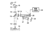
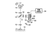
図1は、この発明の一実施の形態に係る顕微鏡の要部を示すもので、顕微鏡本体のステージ10には、標本11が載置される。このステージ11上には、対物レンズ12が対向配置され、この対物レンズ12の光軸上には、ダイクロイックミラー13、吸収フィルタ14、結像レンズ15、プリズム16を介して接眼レンズ17が配設される。また、上記ダイクロイックミラー13の反射光軸(照明光軸)A上には、励起フィルタ18、視野絞り投影レンズ19、デジタル微小ミラー装置20が配設される。そして、このデジタル微小ミラー装置20の入射路には、反射部材である反射ミラー21、コレクタレンズ22を介して、例えば水銀ランプで構成される光源23が配設される。
【0016】
上記デジタル微小ミラー装置20としては、例えば米国特許5,061,049号公報に開示されるところのDMD(Digital Micromirror Davices)で、図2に示すように角度位置が静電的に変化される複数の微小ミラー201を、2次元空間的に配列し、各微小ミラー201に対する印加電圧をオン・オフ制御(印加電圧の制御)することにより、各微小ミラー201が夫々独立に角度制御できるものである。
【0017】
即ち、デジタル微小ミラー装置20は、その複数の微小ミラー201が、照明光軸Aに対して垂直で、対物レンズ12の光軸に対して垂直に投影されるように上記標本の共役位置に配置され、駆動制御部24を介して複数の微小ミラー201が、夫々独立して10マイクロ秒オーダーの応答速度で選択的にオン・オフ切換制御される。
【0018】
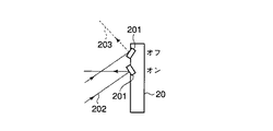
例えば複数の微小ミラー201は、1024個×768個が配列され(但し、図2中では、図の都合上、2個のみを図示)、それぞれの垂線に対して予め決められた傾斜角度α(例えば10°)に個別に傾斜されて配設され、所望の面積(DMDに依存、例えば20μm以下の方形状)に形成される。そして、これら複数の微小ミラー201は、例えばオン制御された状態で光源23からの照明光を照明光軸Aに案内し、オフ制御された状態で光源23からの照明光を退避光軸(外部)203方向に案内するように配設される。
【0019】
ここで、照明光軸A上に配置される視野絞り投影レンズ19は、その焦点位置が対物レンズ12の瞳位置及び微小ミラー201の面上になるように配設される。即ち、視野絞り投影レンズ19は、微小ミラー201を最適な大きさで投影するように、その焦点距離f1が50mm〜300mm程度の1枚以上のレンズで形成されるレンズ群で構成される。これは焦点距離f1が50mm以下では、実構成を取ることが困難なことと、焦点距離f1が300mmを超えると、標本11面上に投影される投影倍率が小さくなりすぎて、使い勝手のよい視野を確保することが困難となると共に、照明光が暗くなるためである。本実施の形態では、例えばf1=170mmを使用する。
【0020】
また、デジタル微小ミラー装置20は、標本11の観察像を撮像する図示しない撮像部の撮像素子のサイズとの関係が、結像レンズ15の焦点距離をf2とし、撮像素子の対角サイズをCとし、配列された複数の微小ミラー201の対角サイズをDとすると、
0.3<f2/f1<5
0.3<C/D<6.6
の関係を満足すると、容易な配置構成が可能となる。本実施の形態では、例えばf2=180mmの焦点距離を用いている。
【0021】
上記構成において、光源23から照射された照明光は、コレクタレンズ22により集光され、反射ミラー21で反射された後、デジタル微小ミラー装置20に導かれる。ここで、デジタル微小ミラー装置20は、その微小ミラー201がオンになっているものが照明光軸A方向へ反射させて投影レンズ19に出力する。この際、微小ミラー201のうちオフになっているものは、退避光軸203方向に反射させて照明として使用されない。
【0022】
上記視野絞り投影レンズ19に導かれた照明光は、励起フィルタ18により標本11の蛍光物質を励起するのに適切な光りに撰択された後、ダイクロイックミラー13により反射され、対物レンズ12により標本11に照射される。ここで、標本11は、照射された照射光に基づいた蛍光を発生する。
【0023】
標本11から発した蛍光は、上記対物レンズ12により集光され、ダイクロイックミラー13を透過して、吸収フィルタ14により蛍光が選択的に透過され、結像レンズ15により結像されて、プリズム16により偏向され、接眼レンズ17により入射される。この接眼レンズ17で観察される光学像は、例えば上記撮像部(図示せず)等に導かれて観察画像として取得することもできる。
【0024】
この際、デジタル微小ミラー装置20の各微小ミラー201の像は、視野絞り投影レンズ19と対物レンズ12により標本11のピント面に結像される。ここで、オン制御された状態の微小ミラー201の像は、照明光の反射光が標本11面まで導かれているため明るく投影され、オフ制御された状態の微小ミラー201の像は、照明光の反射光が標本11面に導かれないために、真暗に投影される。つまり標本11上ではデジタル微小ミラー装置20の各微小ミラー201の像は、そのオン・オフ制御状態により明暗として投影されるため、明の部分のみが照明されている状態となり、微小ミラー201のオン・オフ切換制御によって、標本11の部分的な照明が可能となる。
【0025】
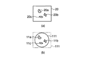
例えば図3(a)は、デジタル微小ミラー装置20の制御状態を示す図で、領域20a、20b、20cに対応する微小ミラー201のみがオン制御の状態を示し、その光が図3(b)に示すように標本11面上の観察視野111の領域11a、11b、11cに投影される。ここで、デジタル微小ミラー装置20の微小ミラー201を制御することにより、観察視野111内の、領域11a、11b、11cの部分のみを順に照明するように制御することも可能である。
【0026】
なお、デジタル微小ミラー装置20としては、その微小ミラー201を最小単位とした制御で可能であれば領域数に制限は無く、その大きさや形状も任意に可変設定するように制御することも可能である。そして、このデジタル微小ミラー装置20の使用形態としては、例えば微小ミラー201をすべてオフ制御すると、照明光を全て遮断できることにより、高速のシャッターとして、使用することもできる。
【0027】
また、蛍光観察を行う場合は、視野に相当する部分の微小ミラー201のみをオン制御することで、視野絞りとして使用できる。そして、標本11として、例えばシャーレ内に培養された複数の細胞のうち、一つの細胞のみを観察したい場合は、その細胞に対応する部分(例えば領域11a)のみを照明してやることで、観察対象以外の細胞へなんら影響(腿色等)を与えることなく、目的の細胞の観察が可能となる。
【0028】
さらに、FRAP観察を行う場合には、デジタル微小ミラー装置20を制御することで、褪色させる範囲(位置、形状、大きさ)を指定し、照明光を一定時間照射し部分的に褪色させる。その後、デジタル微小ミラー装置20の視野111に対応する範囲の微小ミラー201を全てオン制御し、蛍光観察を行い、褪色した部分への周囲の蛍光色素の拡散を観察する。この時、褪色のための部分領域照明状態と、視野全体照明状態は、デジタル微小ミラー装置20の応答速度である数十マイクロ秒オーダーでの切換が可能で、例えば細胞内の高速な拡散でもタイムラグが非常に少ない状態で観察できる。
【0029】
また、褪色時の照明と蛍光観察時の照明の波長を、例えば電動フィルターホイールや電動蛍光キューブターレット等の顕微鏡で、既知な図示しない手段で、励起フィルタ18やダイクロイックミラー13を切換えることで変更することも可能である。そして、同様の制御でケージド試薬を用いた観察を行うことも可能である。さらに、カルシウム指示薬等で、細胞の蛍光の変化を明るさ情報として取得したい場合には、対象とする細胞に相当する一部分(例えば領域11b)のみを照明し、観察光学系に例えば図示しないPMTを配置して受光することで、所望の部分のみのデータが測光できる。
【0030】
また、複数の細胞に対応した領域、例えば領域11a、11b、11cの順に照明光を順次切換えてやることで、複数の細胞の個々の状況をタイムラグが、非常に少ない状態で測光することができる。
【0031】
このように、上記顕微鏡では、光源23から放射され、反射ミラー21を介して入射された照明光を、オン・オフ切換制御により選択的に反射制御して標本11面上の任意の位置に、照明するための複数の微小ミラー201からなる照明手段を、標本11と共役位置で、且つ、対物レンズ12で形成される光軸に垂直に配置するように構成した。
【0032】
これによれば、反射構造を採用していることで、光源23から照射される照明光のコントラストが高く高精度な色特性を確保することができ、しかも、デジタル微小ミラー装置20の微小ミラー201のオン・オフ制御により、光源23から放射された照明光を、標本11面上の所望の位置に、所望の大きさと、所望の形状で照射することができるため、照明光の迅速にして高精度な調整制御が可能となり、観測精度の向上が図れる。また、これによれば、照明光調整時に機械的な振動が発生しないことで、観察像に振動の影響を受けることなく、高精度な観察が実現される。特に、観察形態として、蛍光観察時に、有益な効果が得られる。
【0033】
また、この発明は、上記実施の形態に限ることなく、その他、図4乃至図13に示すように構成しても良い。但し、図4乃至図13においては、上記図1乃至図3と同一部分について、同一符号を付して、その詳細な説明を省略する。
【0034】
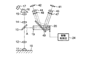
図4は、反射ミラーとして、50%透過、50%反射のハーフミラー31を、デジタル微小ミラー装置20とコレクタレンズ22との間に配置するように構成したものである。本実施の形態によれば、照明光をさげるために、反射部材を遠ざける必要がないためデジタル微小ミラー装置20と視野絞り投影レンズ19との配置間隔を、短くすることが可能となり、視野絞り投影レンズ19の焦点距離の自由度を向上させることができるため、デジタル微小ミラー装置20の標本11面への投影倍率の自由度が高められる。
【0035】
図5は、デジタル微小ミラー装置20の入射軸に対応して第1及び第2の光源41、42を、それぞれ第1及び第2のコレクタレンズ43、44、第1及び第2の反射ミラー45、46を介して対向配置する。そして、第1のコレクタレンズ43と第1の反射ミラー45との間の光軸上、及び第2のコレクタレンズ44と第2の反射ミラー46との間の光軸上には、特性の異なる第1及び第2の励起フィルタ47、48を介在するように構成したものである。
【0036】
上記構成により、第1の光源41から放射された照明光は、第1のコレクタレンズ43により集光され、第1の励起フィルタ47により選択的に透過された後、反射ミラー45で反射されデジタル微小ミラー装置20に導かれる。ここで、デジタル微小ミラー装置20は、その微小ミラー201がオン制御状態で、照明光を照明光軸A方向に反射させて視野絞り投影レンズ19に案内する。そして、デジタル微小ミラー装置20の微小ミラー201かオフ制御状態では、退避光軸203方向へ反射され、照明として使用されない。
【0037】
この際、第2の光源42から放射された照明光は、第2のコレクタレンズ44により集光され、第2の励起フィルタ48により選択的に透過された後、第2の反射ミラー46で反射されデジタル微小ミラー装置20に導かれる。ここで、デジタル微小ミラー装置20は、その微小ミラー201がオフ制御状態で、照明光を照明光軸A方向に反射させて視野絞り投影レンズ19に案内する。そして、デジタル微小ミラー装置20の微小ミラー201がオン制御状態では、照明光が退避光軸203方向へ反射され、照明として使用されない。
【0038】
これにより、例えば図6に示すように視野11内のデジタル微小ミラー装置20の微小ミラー201が、オン制御になっている状態に対応する任意領域Gは、第1の光源41からの照明光で照明され、デジタル微小ミラー装置20の微小ミラー201がオフ制御になっている状態に対応する領域Hは、第2の光源からの照明光で照明される。
【0039】
そこで、上記第1及び第2の励起フィルタ47、48を、例えば異なる波長帯域のバンドパスフィルタで構成した場合には、領域Gと領域Hを異なる波長で照明することができる。このような構成において、ケージド蛍光試薬による観察を行う場合には、その領域Gをケージド解除の波長で照明し、領域Hを解除後の蛍光観察の波長で照明することで、まさに解除しながら同時にタイムラグ無しに拡散の様子を観察することができる。
【0040】
ここで、例えばデジタル微小ミラー装置20の全微小ミラー201を同時にオン・オフ切換制御することにより、2つの波長の照明光を、数十マイクロ秒オーダーの高速、かつ、無振動に切換えることができるため、目視観察では、あたかも2波長同時に照明しているかの如く観察できる。このように本実施の形態によれば、観察形態の多様化が図れて使い勝手の向上を図ることができる。
【0041】
図7は、図5の第1及び第2の反射ミラー45、46を、ハーフミラー49で兼用するように配置構成したものである。本実施の形態によれば、第1及び第2の光源の配置位置を変更することが可能となり、空間的配置構成のバリエーションを得ることが可能となり、設計の自由度の向上が図れる。
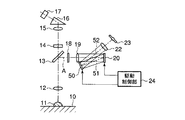
【0042】
また、図8は、開口絞りと共役位置に第2のデジタル微小ミラー装置50を上記デジタル微小ミラー装置20に対向させて配設し、この第2のデジタル微小ミラー装置50の後段には、上記コレクタレンズ22を介して光源が配設するように構成したものである。ここで、51は、上記デジタル微小ミラー装置20の微小ミラー201がオン制御状態での照明光軸で、52は、第2のデジタル微小ミラー装置50の微小ミラー201がオン制御の状態での照明光軸である。
【0043】
上記構成において、光源23から放射された照明光は、コレクタレンズ22により集光され、第2のデジタル微小ミラー装置50へ導かれる。第2のデジタル微小ミラー装置50の微小ミラー201がオン状態で、照明光は、照明光軸51方向に反射され、デジタル微小ミラー装置20へ導かれる。このデジタル微小ミラー装置20の微小ミラー201がオン状態で、照明光は、光軸A方向へ反射され、標本11を照明する。
【0044】
ここで、第2のデジタル微小ミラー装置50は、開口絞りと共役位置に置かれているため、各微小ミラー201の制御によって、開口絞り位置に様々な形状の絞りを入れたことと同義になり、一般的に絞りによって与えられる顕微鏡の照明変調効果を自由に得ることができる。例えば第2のデジタル微小ミラー装置50上の光軸中心に円形の微小ミラー201のオン領域を作ってやり、大きさを制御することで、明るさ調節が可能となる。また、開口絞り径の半分に相当する微小ミラー201をオン制御にすることで、偏射照明が可能となる。本実施の形態によれば、デジタル微小ミラー装置20の効果に加え、第2のデジタル微小ミラー装置50により開口絞りの機能も加えることができる。
【0045】
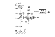
図9は、図1の配置構成において、そのコレクタレンズ22及び光源23の配置を変更し、図10は、デジタル微小ミラー装置20の後段に反射ミラー21を配設するようにして、小型化の促進を図るように構成したものである。
【0046】
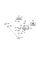
また、図11は、ハーフミラーコーティング面601及び全反射面602を有したプリズム60を、その全反射面602をデジタル微小ミラー装置に対向させ、且つそのハーフミラーコーティング面601を視野絞り投影レンズ19に対向させた状態で、コレクタレンズ22及び視野絞り投影レンズ19との間に介在するように構成したものである。本実施の形態によれば、反射面の距離を短くすることができるので、小型化の促進を図ることが可能となる。
【0047】
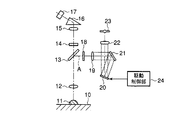
図12は、デジタル微小ミラー装置20とコレクタレンズ22との間に配設される反射ミラー21を削除し、光源23からの照明光をコレクタレンズ22で集光して、直接的にデジタル微小ミラー装置20に導くように構成したもので、部品点数の軽減が図れて小型化の促進が図れる。
【0048】
図13は、倒立式顕微鏡に適用したもので、接眼レンズ17と結像レンズ15との間に配設されるプリズム16に代えてリレーレンズ70及び全反射ミラー71を配設するように構成したものである。
【0049】
また、上記実施の形態では、デジタル微小ミラー装置の微小ミラーをオン状態で照明軸方向に位置され、そのオフ状態で、退避軸方向に対応するように構成した場合で説明したが、これに限ることなく、オン状態で退避軸方向に対応され、オフ状態で照明軸方向に対応するように構成することも可能である。
【0050】
さらに、上記実施の形態では、照明光を反射するデジタル微小ミラー装置を用いて構成した場合で説明したが、これに限ることなく、反射型の液晶素子を用いて構成することも可能である。
【0051】
よって、この発明は、上記実施の形態に限ることなく、その他、実施段階ではその要旨を逸脱しない範囲で種々の変形を実施し得ることが可能である。さらに、上記実施形態には、種々の段階の発明が含まれており、開示される複数の構成要件における適宜な組合せにより種々の発明が抽出され得る。
【0052】
例えば実施形態に示される全構成要件から幾つかの構成要件が削除されても、発明が解決しようとする課題の欄で述べた課題が解決でき、発明の効果で述べられている効果が得られる場合には、この構成要件が削除された構成が発明として抽出され得る。
【0053】
また、上述した実施の形態では、照明用の光源に水銀灯やキセノンランプ、ハロゲンランプなどの白色光源を用いていたが、照明用の光源はこれらに限られるものではなく、例えば図14に示すようにレーザ光源81を用いることもできる。
【0054】
図14の構成は、基本的に前述した実施の形態と大きく異なるものではないため詳細な説明は省略するが、図14に示される顕微鏡の構成は、光源にレーザ光源81を用いるために、光束を広げるためにレーザ光源81から発せられるレーザ光の光軸上に凹凸レンズからなるビームエクスパンダー82が設けられている点と、白色光源に比べて波長特性が安定しているため、白色光源を用いている場合に必要であった励起フィルタが不要となる点と、レーザ光により励起された標本からの蛍光を撮像するためのカメラ83及び該カメラ83で撮像した画像情報をモニタ84に表示するために画像処理を行うコンピュータ85とを備えている点とが前述した実施の形態の構成と異なる。
【0055】
上述した構成によれば、各種波長の選択には規制が生じるが、白色光源に比べてより明るい照明を実現することができる。
【0056】
【発明の効果】
以上詳述したように、この発明によれば、照明光の高精度な色特性を確保したうえで、照明光の迅速にして高精度な調整制御を実現し得るようにして、観測精度の向上を図った顕微鏡を提供することができる。
【図面の簡単な説明】
【図1】この発明の一実施の形態に係る顕微鏡の要部を示した構成図である。
【図2】図1のデジタル微小ミラー装置の詳細を説明するために示した構成説明図である。
【図3】図1の観察動作を説明するために示した動作説明図である。
【図4】この発明の他の実施の形態に係る顕微鏡の要部を示した構成図である。
【図5】この発明の他の実施の形態に係る顕微鏡の要部を示した構成図である。
【図6】図5の観察動作を説明するために示した動作説明図である。
【図7】この発明の他の実施の形態に係る顕微鏡の要部を示した構成図である。
【図8】この発明の他の実施の形態に係る顕微鏡の要部を示した構成図である。
【図9】この発明の他の実施の形態に係る顕微鏡の要部を示した構成図である。
【図10】この発明の他の実施の形態に係る顕微鏡の要部を示した構成図である。
【図11】この発明の他の実施の形態に係る顕微鏡の要部を示した構成図である。
【図12】この発明の他の実施の形態に係る顕微鏡の要部を示した構成図である。
【図13】この発明の他の実施の形態に係る顕微鏡の要部を示した構成図である。
【図14】この発明の他の実施の形態に係る顕微鏡の要部を示した構成図である。
【符号の説明】
10 … ステージ。
11 … 標本。
12 … 対物レンズ。
13 … ダイクロイックミラー。
14 … 吸収フィルタ。
15 … 結像レンズ。
16 … プリズム。
17 … 接眼レンズ。
18 … 励起フィルタ。
19 … 視野絞り投影レンズ。
20 … デジタル微小ミラー装置。
201 … 微小ミラー。
21 … 反射ミラー。
22 … コレクタレンズ。
23 … 光源。
24 … 駆動制御部。
31 … ハーフミラー。
41、42 … 第1及び第2の光源。
43、44 … 第1及び第2のコレクタレンズ。
45、46 … 第1及び第2の反射ミラー。
47、48 … 第1及び第2の励起フィルタ。
49 … ハーフミラー。
50 … 第2のデジタル微小ミラー装置。
60 … プリズム。
601 … ハーフミラーコーティング面。
602 … 全反射面。
70 … リレーレンズ。
71 … 全反射ミラー。[0001]
BACKGROUND OF THE INVENTION
The present invention relates to a microscope such as a fluorescence microscope having an illumination mechanism, for example.
[0002]
[Prior art]
In general, a microscope having Koehler illumination is provided with a field stop function for illuminating the same range as the observation range. When a part of the field of view is to be observed, such as during fluorescence observation, the other part of the sample is deteriorated, and the field stop is made smaller to prevent fluorescence fading. The method of illuminating only the part is taken.
[0003]
In addition, recently, in fluorescence observation, the inside of the visual field is partially faded, and the return state is observed, so that FRAP (Fluorescence Recovery After Photography), FLIP (Fluorescence Loss In Photoleaching), A means for observing the diffusion and the like is performed by dyeing with a Caged reagent that has scientifically confined characteristics, and partially illuminating it with illumination light. For this reason, at the time of fluorescence observation, the request | requirement which illuminates a part in a visual field with arbitrary magnitude | sizes and shapes is increasing.
[0004]
As a method of illuminating a part of the field of view, there is a method of realizing partial illumination by detachably disposing a pinhole or a slit at a field stop position (a position conjugate with the sample) of the light receiving illumination optical system.
[0005]
Incidentally, an iris diaphragm whose diameter can be mechanically changed is generally used for the field diaphragm. For example, Japanese Patent Application Laid-Open Nos. 7-134250 and 2000-502472 disclose a method in which a transmissive liquid crystal element (LCD) is arranged at a stop position and used as a stop by controlling the density. By adopting this method, not only the function of matching the observation range and the illumination range, but also a part of the field of view can be illuminated with an arbitrary size and shape.
However, in this liquid crystal diaphragm method, the polarizing plate is used for the liquid crystal element, so that the transmittance is low, the amount of illumination light decreases, and the color characteristics of the transmitted light change even in the state of 100% transmission control. Therefore, the observation accuracy is lowered. Furthermore, UV light may be used for fluorescent illumination, but it is difficult to use a liquid crystal that has low UV transmittance and low autofluorescence.
[0006]
Also, according to this, since the response speed at the time of control is on the order of several tens of milliseconds, when observing temporal changes in cells while switching the illumination position and shape in the visual field, the response speed is highly accurate. There is a problem that observation is difficult.
[0007]
In the Japanese translations of PCT publication No. 2000-502472 described as the above-mentioned conventional example, the DMD (digital mirror device) having a different light modulation structure is simply used in place of the liquid crystal element (LCD) in the claims. There is a description. However, in the description of the embodiments of this publication, the specific configuration of the illumination device using DMD that can be implemented by those skilled in the art is not disclosed or suggested at all, and the combined arrangement itself is not disclosed. There is nothing.
[0008]
[Problems to be solved by the invention]
As described above, in the conventional liquid crystal diaphragm type microscope, the transmittance is poor, the color characteristics of transmitted light are changed, and the response characteristics of the control system are poor, so that satisfactory observation accuracy is not achieved. It is clear that.
[0009]
The present invention has been made in view of the above circumstances, and a microscope having high observation accuracy capable of realizing high-precision adjustment control of illumination light quickly while ensuring high-precision color characteristics of illumination light. The purpose is to provide.
[0010]
[Means for Solving the Problems]
The present invention generates an objective lens disposed opposite to a specimen and illumination light that illuminates the specimen.First and secondLighting means;A field stop projection lens on the illumination optical axis and disposed between the first and second illumination means and the objective lens;A plurality of minute light deflecting units arranged at a position conjugate with the sample and on the optical axis passing through the objective lens, and selectively deflectable in conjunction with voltage control.Configured,The irradiation on the specimen surfaceFirst and secondAn optical deflection element array for independently deflecting illumination light from the illumination means, and the optical deflection element arraySelectively voltageA control unit to control;First and second reflecting members that are on the illumination optical axis and are disposed between the light deflection element array and the first and second illumination means, and on the illumination optical axis And first and second excitation filters disposed between the light deflection element array and the first and second illumination means,
A microscope was constructed.
[0013]
According to the above configuration, the optical deflection element array includes the plurality of minute optical deflection units.Field of viewBy projecting on the sample surface arranged at the conjugate position through the aperture projection lens, the voltage control of the minute light deflection unit selectivelyFirst and secondThe illumination light emitted from the illumination meansFirst and second excitation filters; andThrough the reflective memberField of viewIrradiate a desired position on the sample surface through the aperture projection lens with a desired size and a desired shape. As a result, while ensuring the color characteristics of the illumination light emitted from the illumination means, it is possible to adjust the illumination light quickly and with high accuracy, thereby improving the observation accuracy.
[0014]
DETAILED DESCRIPTION OF THE INVENTION
Hereinafter, embodiments of the present invention will be described in detail with reference to the drawings.
[0015]
FIG. 1 shows a main part of a microscope according to an embodiment of the present invention. A
[0016]
The
[0017]
That is, the
[0018]
For example, a plurality of
[0019]
Here, the field
[0020]
Further, in the
0.3 <f2 / f1 <5
0.3 <C / D <6.6
If the above relationship is satisfied, an easy arrangement configuration is possible. In the present embodiment, for example, a focal length of f2 = 180 mm is used.
[0021]
In the above configuration, the illumination light emitted from the
[0022]
The illumination light guided to the field
[0023]
The fluorescence emitted from the
[0024]
At this time, the image of each
[0025]
For example, FIG. 3A is a diagram showing the control state of the
[0026]
The
[0027]
In addition, when performing fluorescence observation, it can be used as a field stop by turning on only the
[0028]
Furthermore, when performing FRAP observation, the
[0029]
Further, the wavelength of illumination during fading and illumination during fluorescence observation is changed by switching the
[0030]
In addition, by sequentially switching the illumination light in the order corresponding to the plurality of cells, for example, the
[0031]
As described above, in the microscope, the illumination light emitted from the
[0032]
According to this, by adopting the reflection structure, it is possible to ensure high-accuracy color characteristics with high contrast of illumination light emitted from the
[0033]
Further, the present invention is not limited to the above-described embodiment, but may be configured as shown in FIGS. However, in FIGS. 4 to 13, the same parts as those in FIGS. 1 to 3 are denoted by the same reference numerals, and detailed description thereof is omitted.
[0034]
FIG. 4 shows a configuration in which a 50% transmission and 50%
[0035]
FIG. 5 shows the first and second
[0036]
With the above configuration, the illumination light emitted from the
[0037]
At this time, the illumination light emitted from the second
[0038]
Thereby, for example, as shown in FIG. 6, the arbitrary region G corresponding to the state in which the
[0039]
Therefore, when the first and second excitation filters 47 and 48 are constituted by bandpass filters having different wavelength bands, for example, the region G and the region H can be illuminated with different wavelengths. In such a configuration, when observation with a caged fluorescent reagent is performed, the region G is illuminated with the wavelength of the caged release, and the region H is illuminated with the wavelength of the fluorescence observation after the release. The state of diffusion can be observed without time lag.
[0040]
Here, for example, by simultaneously controlling on / off switching of all the
[0041]
FIG. 7 shows a configuration in which the first and second reflection mirrors 45 and 46 of FIG. According to the present embodiment, it is possible to change the arrangement positions of the first and second light sources, to obtain a variation of the spatial arrangement configuration, and to improve the degree of freedom in design.
[0042]
Further, in FIG. 8, the second
[0043]
In the above configuration, the illumination light emitted from the
[0044]
Here, since the second
[0045]
9 changes the arrangement of the
[0046]
FIG. 11 shows a
[0047]
In FIG. 12, the
[0048]
FIG. 13 shows an application to an inverted microscope, in which a
[0049]
In the above-described embodiment, the description has been given of the case where the micromirror of the digital micromirror device is configured to be positioned in the illumination axis direction in the on state and to correspond to the retracting axis direction in the off state. Instead, it can be configured to correspond to the retracting axis direction in the on state and correspond to the illumination axis direction in the off state.
[0050]
Furthermore, in the above-described embodiment, the case where the digital micromirror device that reflects illumination light is used has been described. However, the present invention is not limited to this, and a configuration using a reflective liquid crystal element is also possible.
[0051]
Therefore, the present invention is not limited to the above-described embodiment, and various modifications can be made without departing from the scope of the invention at the stage of implementation. Further, the above embodiments include inventions at various stages, and various inventions can be extracted by appropriately combining a plurality of disclosed constituent elements.
[0052]
For example, even if some constituent elements are deleted from all the constituent elements shown in the embodiment, the problems described in the column of problems to be solved by the invention can be solved, and the effects described in the effects of the invention can be obtained. In some cases, a configuration from which this configuration requirement is deleted can be extracted as an invention.
[0053]
In the above-described embodiment, a white light source such as a mercury lamp, a xenon lamp, or a halogen lamp is used as the illumination light source. However, the illumination light source is not limited to these, and for example, as shown in FIG. A
[0054]
The configuration of FIG. 14 is basically not significantly different from the above-described embodiment, and thus detailed description thereof is omitted. However, the configuration of the microscope shown in FIG. In order to broaden the range, the
[0055]
According to the configuration described above, the selection of various wavelengths is restricted, but it is possible to realize brighter illumination than a white light source.
[0056]
【The invention's effect】
As described above in detail, according to the present invention, the high-precision color characteristics of the illumination light can be ensured, and the illumination light can be quickly adjusted to achieve high-precision adjustment control, thereby improving the observation accuracy. The microscope which aimed at can be provided.
[Brief description of the drawings]
FIG. 1 is a configuration diagram showing a main part of a microscope according to an embodiment of the present invention.
FIG. 2 is an explanatory diagram of a configuration shown for explaining details of the digital micromirror device of FIG. 1;
FIG. 3 is an operation explanatory diagram shown for explaining the observation operation of FIG. 1;
FIG. 4 is a configuration diagram showing a main part of a microscope according to another embodiment of the present invention.
FIG. 5 is a configuration diagram showing a main part of a microscope according to another embodiment of the present invention.
6 is an operation explanatory diagram shown for explaining the observation operation of FIG. 5. FIG.
FIG. 7 is a configuration diagram showing a main part of a microscope according to another embodiment of the present invention.
FIG. 8 is a configuration diagram showing a main part of a microscope according to another embodiment of the present invention.
FIG. 9 is a configuration diagram showing a main part of a microscope according to another embodiment of the present invention.
FIG. 10 is a configuration diagram showing a main part of a microscope according to another embodiment of the present invention.
FIG. 11 is a configuration diagram showing a main part of a microscope according to another embodiment of the present invention.
FIG. 12 is a configuration diagram showing a main part of a microscope according to another embodiment of the present invention.
FIG. 13 is a configuration diagram showing a main part of a microscope according to another embodiment of the present invention.
FIG. 14 is a configuration diagram showing a main part of a microscope according to another embodiment of the present invention.
[Explanation of symbols]
10 ... Stage.
11… Specimen.
12 ... Objective lens.
13 ... Dichroic mirror.
14: Absorption filter.
15: Imaging lens.
16 ... Prism.
17 ... Eyepiece.
18: Excitation filter.
19 ... Field stop projection lens.
20: Digital micromirror device.
201 ... A micro mirror.
21 ... Reflective mirror.
22 ... Collector lens.
23: Light source.
24: Drive control unit.
31 ... Half mirror.
41, 42... First and second light sources.
43, 44... First and second collector lenses.
45, 46: first and second reflecting mirrors.
47, 48... First and second excitation filters.
49 ... Half mirror.
50: Second digital micromirror device.
60 ... Prism.
601: Half mirror coating surface.
602: Total reflection surface.
70: Relay lens.
71: Total reflection mirror.
Claims (3)
前記標本を照明する照明光を発生する第1、及び第2の照明手段と、
照明光軸上にあって、且つ前記第1、及び第2の照明手段と前記対物レンズの間に配置された視野絞り投影レンズと、
前記標本と共役位置で、且つ前記対物レンズを通る光軸上の位置に配置され、電圧制御に連動して選択的に偏向制御可能な複数の微小光偏向部で構成され、前記標本面上に照射される前記第1、及び第2の照明手段からの照明光を夫々独立して偏向させる光偏向素子アレイと、
前記光偏向素子アレイを選択的に電圧制御する制御部と、
前記照明光軸上にあって、且つ前記光偏向素子アレイと前記第1、及び第2の照明手段との間に配置される第1、及び第2の反射部材と、
前記照明光軸上にあって、且つ前記光偏向素子アレイと前記第1、及び第2の照明手段との間に配置される第1、及び第2の励起フィルタと、
を具備することを特徴とする顕微鏡。An objective lens placed opposite the specimen;
First and second illumination means for generating illumination light for illuminating the specimen;
A field stop projection lens on the illumination optical axis and disposed between the first and second illumination means and the objective lens ;
It is arranged at a position conjugate with the sample and on the optical axis passing through the objective lens, and is composed of a plurality of minute optical deflecting units that can selectively control deflection in conjunction with voltage control. A light deflection element array for independently deflecting illumination light from the first and second illumination means to be irradiated;
A controller for selectively controlling the voltage of the optical deflection element array;
Be on the illumination optical axis, the first and second reflecting members are and disposed between the optical deflector element array and the first and second illumination means,
Be on the illumination optical axis, and and the first and second excitation filter is disposed between said light deflecting element array the first and second illumination means,
The microscope characterized by comprising.
Priority Applications (3)
| Application Number | Priority Date | Filing Date | Title |
|---|---|---|---|
| JP2001304123A JP5048899B2 (en) | 2001-09-28 | 2001-09-28 | microscope |
| US10/252,434 US6898004B2 (en) | 2001-09-28 | 2002-09-23 | Microscope system |
| DE10244431A DE10244431A1 (en) | 2001-09-28 | 2002-09-24 | microscope system |
Applications Claiming Priority (1)
| Application Number | Priority Date | Filing Date | Title |
|---|---|---|---|
| JP2001304123A JP5048899B2 (en) | 2001-09-28 | 2001-09-28 | microscope |
Publications (2)
| Publication Number | Publication Date |
|---|---|
| JP2003107361A JP2003107361A (en) | 2003-04-09 |
| JP5048899B2 true JP5048899B2 (en) | 2012-10-17 |
Family
ID=19124094
Family Applications (1)
| Application Number | Title | Priority Date | Filing Date |
|---|---|---|---|
| JP2001304123A Expired - Fee Related JP5048899B2 (en) | 2001-09-28 | 2001-09-28 | microscope |
Country Status (3)
| Country | Link |
|---|---|
| US (1) | US6898004B2 (en) |
| JP (1) | JP5048899B2 (en) |
| DE (1) | DE10244431A1 (en) |
Families Citing this family (44)
| Publication number | Priority date | Publication date | Assignee | Title |
|---|---|---|---|---|
| EP1333305B8 (en) * | 2002-02-04 | 2007-08-01 | Carl Zeiss Surgical GmbH | Stereoscopic examination system, stereoscopic image processing apparatus and operating method |
| JP2004309702A (en) * | 2003-04-04 | 2004-11-04 | Olympus Corp | Microscope |
| US7580178B2 (en) * | 2004-02-13 | 2009-08-25 | Angstrom, Inc. | Image-guided microsurgery system and method |
| US20060066842A1 (en) * | 2004-09-30 | 2006-03-30 | Saunders Winston A | Wafer inspection with a customized reflective optical channel component |
| JP2006171024A (en) * | 2004-12-10 | 2006-06-29 | Olympus Corp | Multi-point fluorescence spectrophotometry microscope and multi-point fluorescence spectrophotometry method |
| US20060158668A1 (en) * | 2005-01-20 | 2006-07-20 | Eastman Kodak Company | Method and apparatus for increasing color gamut of a three color primary additive display device |
| JP2006220818A (en) * | 2005-02-09 | 2006-08-24 | Hamamatsu Univ School Of Medicine | Confocal microscope |
| DE102006001427B4 (en) * | 2005-03-04 | 2021-02-04 | Leica Microsystems Cms Gmbh | Method for illuminating a sample |
| JP4526988B2 (en) * | 2005-03-23 | 2010-08-18 | 株式会社ブイ・テクノロジー | Minute height measuring method, minute height measuring apparatus and displacement unit used therefor |
| JP4538633B2 (en) * | 2005-03-29 | 2010-09-08 | 国立大学法人浜松医科大学 | DLP slit optical scanning microscope |
| JP2006317836A (en) * | 2005-05-16 | 2006-11-24 | Olympus Corp | Scanning microscope |
| US7593156B2 (en) * | 2005-08-26 | 2009-09-22 | Leica Microsystems (Schweiz) Ag | Microscope with micro-mirrors for optional deflection and/or beam splitting |
| DE102005040471B4 (en) * | 2005-08-26 | 2007-06-21 | Leica Microsystems (Schweiz) Ag | microscope |
| JP4725967B2 (en) * | 2006-02-09 | 2011-07-13 | 株式会社ブイ・テクノロジー | Minute height measuring device and displacement meter unit |
| DE102006022592B4 (en) * | 2006-05-15 | 2008-02-07 | Leica Microsystems (Schweiz) Ag | Microscope with lighting unit |
| DE102006025149A1 (en) * | 2006-05-30 | 2007-12-06 | Leica Microsystems (Schweiz) Ag | Optical device with increased depth of field |
| DE102006027836B4 (en) * | 2006-06-16 | 2020-02-20 | Carl Zeiss Microscopy Gmbh | Microscope with auto focus device |
| JP5021254B2 (en) * | 2006-09-06 | 2012-09-05 | オリンパス株式会社 | Control method of microscope apparatus, microscope apparatus |
| JP4891057B2 (en) * | 2006-12-27 | 2012-03-07 | オリンパス株式会社 | Confocal laser scanning microscope |
| JP5137488B2 (en) * | 2007-07-25 | 2013-02-06 | オリンパス株式会社 | Laser irradiation apparatus and laser processing system using the same |
| JP5393406B2 (en) * | 2009-11-06 | 2014-01-22 | オリンパス株式会社 | Pattern projector, scanning confocal microscope, and pattern irradiation method |
| DE102010026213A1 (en) | 2010-07-06 | 2012-01-12 | Carl Zeiss Ag | Method for illuminating biological tissue of pupil of eyes of patient in e.g. operation microscope, involves carrying out alteration of intensity distribution such that location in object field is illuminated with high intensity |
| CN103168236B (en) | 2010-08-23 | 2016-01-20 | 哈佛大学管理委员会 | For the light genetics probe that membrane potential measures |
| US9207237B2 (en) | 2010-08-23 | 2015-12-08 | President And Fellows Of Harvard College | Systems, methods, and workflows for optogenetics analysis |
| JP6351951B2 (en) * | 2013-10-22 | 2018-07-04 | 浜松ホトニクス株式会社 | Total reflection light irradiation device |
| JP2017520237A (en) | 2014-04-22 | 2017-07-27 | キュー−ステート バイオサイエンシーズ, インコーポレイテッドQ−State Biosciences, Inc. | Diagnostic methods for neuronal disorders |
| US9518103B2 (en) | 2014-06-18 | 2016-12-13 | President And Fellows Of Harvard College | Optogenetic probes for measuring membrane potential |
| US10077463B2 (en) | 2015-01-15 | 2018-09-18 | President And Fellows Of Harvard College | Optical selection of cells |
| US10048275B2 (en) | 2015-03-13 | 2018-08-14 | Q-State Biosciences, Inc. | Cardiotoxicity screening methods |
| US10288863B2 (en) | 2015-05-21 | 2019-05-14 | Q-State Biosciences, Inc. | Optogenetics microscope |
| JP2019066706A (en) * | 2017-10-02 | 2019-04-25 | ソニー株式会社 | Fluorescence microscope device and fluorescence microscope system |
| CA3065780A1 (en) | 2018-01-08 | 2019-07-11 | Illumina, Inc. | Systems and devices for high-throughput sequencing with semiconductor-based detection |
| NL2020619B1 (en) | 2018-01-16 | 2019-07-25 | Illumina Inc | Dual optical grating slide structured illumination imaging |
| NL2020620B1 (en) | 2018-01-16 | 2019-07-25 | Illumina Inc | Pattern angle spatial selection structured illumination imaging |
| TWI699559B (en) | 2018-01-16 | 2020-07-21 | 美商伊路米納有限公司 | Structured illumination imaging system and method of creating a high-resolution image using structured light |
| NL2020622B1 (en) | 2018-01-24 | 2019-07-30 | Lllumina Cambridge Ltd | Reduced dimensionality structured illumination microscopy with patterned arrays of nanowells |
| NL2020623B1 (en) | 2018-01-24 | 2019-07-30 | Illumina Inc | Structured illumination microscopy with line scanning |
| CN108519152A (en) * | 2018-04-11 | 2018-09-11 | 中科谱光科技(北京)有限公司 | A kind of projection bloom spectra system |
| DE102018110083A1 (en) | 2018-04-26 | 2019-10-31 | Carl Zeiss Microscopy Gmbh | Optical arrangement for flexible multi-color lighting for a light microscope and method for this purpose |
| NL2021258B1 (en) | 2018-06-14 | 2019-12-20 | Illumina Inc | Device for luminescent imaging |
| TWI718557B (en) | 2018-06-29 | 2021-02-11 | 美商伊路米納有限公司 | Method, system, and non-transitory computer-readable medium for predicting structured illumination parameters |
| JP7380569B2 (en) | 2018-08-09 | 2023-11-15 | ソニーグループ株式会社 | Optical microscope equipment and optical microscope system |
| US10901202B2 (en) | 2018-09-19 | 2021-01-26 | Illumina, Inc. | Structured illumination of a sample |
| IL262619B (en) | 2018-10-25 | 2020-05-31 | Beyeonics Surgical Ltd | System and method to automatically adjust illumination during a microsurgical procedure |
Family Cites Families (6)
| Publication number | Priority date | Publication date | Assignee | Title |
|---|---|---|---|---|
| US5061049A (en) | 1984-08-31 | 1991-10-29 | Texas Instruments Incorporated | Spatial light modulator and method |
| GB9014263D0 (en) * | 1990-06-27 | 1990-08-15 | Dixon Arthur E | Apparatus and method for spatially- and spectrally- resolvedmeasurements |
| US5923466A (en) | 1993-10-20 | 1999-07-13 | Biophysica Technologies, Inc. | Light modulated confocal optical instruments and method |
| JPH07134250A (en) | 1993-11-10 | 1995-05-23 | Nikon Corp | Illuminating light controlling device |
| DE19644662C2 (en) | 1996-10-25 | 2000-04-13 | Leica Microsystems | Illumination device for a microscope |
| ATE272224T1 (en) | 1997-11-17 | 2004-08-15 | Max Planck Gesellschaft | CONFOCAL SPECTROSCOPY SYSTEM AND METHOD |
-
2001
- 2001-09-28 JP JP2001304123A patent/JP5048899B2/en not_active Expired - Fee Related
-
2002
- 2002-09-23 US US10/252,434 patent/US6898004B2/en not_active Expired - Lifetime
- 2002-09-24 DE DE10244431A patent/DE10244431A1/en not_active Ceased
Also Published As
| Publication number | Publication date |
|---|---|
| DE10244431A1 (en) | 2003-04-24 |
| US20030063376A1 (en) | 2003-04-03 |
| JP2003107361A (en) | 2003-04-09 |
| US6898004B2 (en) | 2005-05-24 |
Similar Documents
| Publication | Publication Date | Title |
|---|---|---|
| JP5048899B2 (en) | microscope | |
| JP5244605B2 (en) | microscope | |
| US7359117B2 (en) | Illumination device for microscope | |
| EP2315065B1 (en) | Microscope | |
| JP2012212155A (en) | Method and apparatus for fluorescent confocal microscopy | |
| JP2004109348A (en) | Microscope apparatus | |
| WO2006104184A1 (en) | Dlp type slit scanning microscope | |
| EP2312369A1 (en) | Confocal optical scanner | |
| JP2007334319A (en) | Illuminating device | |
| JP2005345716A (en) | Microscope | |
| JP2004347777A (en) | Total reflection fluorescence microscope | |
| JP4854880B2 (en) | Laser microscope | |
| US6903869B2 (en) | Illumination system for microscopy and observation or measuring method using the same | |
| US6072623A (en) | Slit lamp microscope | |
| JP5209186B2 (en) | Epi-illumination optical system for microscope | |
| CN113056696B (en) | Microscope and microscopic examination method | |
| JP4370404B2 (en) | DLP type evanescence microscope | |
| KR101907845B1 (en) | Transmissive illumination fluorescence microscope comprising Koehler illumination | |
| JP4128387B2 (en) | Microscope equipment | |
| JP6945557B2 (en) | Optical scanning microscope and inspection method | |
| JP2008102535A (en) | Stereo microscope | |
| JP4172212B2 (en) | Microscope specimen illumination method and microscope having illumination apparatus using the same | |
| JP4869606B2 (en) | Laser light irradiation device and microscope device with laser light irradiation device | |
| US11880026B2 (en) | Microscope and method for light-field microscopy with light-sheet excitation and for confocal microscopy | |
| US20060087727A1 (en) | Apparatus, system and method for selective photobleaching, imaging and confocal microscopy |
Legal Events
| Date | Code | Title | Description |
|---|---|---|---|
| A621 | Written request for application examination |
Free format text: JAPANESE INTERMEDIATE CODE: A621 Effective date: 20080825 |
|
| A131 | Notification of reasons for refusal |
Free format text: JAPANESE INTERMEDIATE CODE: A131 Effective date: 20110607 |
|
| A521 | Request for written amendment filed |
Free format text: JAPANESE INTERMEDIATE CODE: A523 Effective date: 20110808 |
|
| A131 | Notification of reasons for refusal |
Free format text: JAPANESE INTERMEDIATE CODE: A131 Effective date: 20111108 |
|
| A521 | Request for written amendment filed |
Free format text: JAPANESE INTERMEDIATE CODE: A523 Effective date: 20120106 |
|
| A02 | Decision of refusal |
Free format text: JAPANESE INTERMEDIATE CODE: A02 Effective date: 20120306 |
|
| A521 | Request for written amendment filed |
Free format text: JAPANESE INTERMEDIATE CODE: A523 Effective date: 20120530 |
|
| A911 | Transfer to examiner for re-examination before appeal (zenchi) |
Free format text: JAPANESE INTERMEDIATE CODE: A911 Effective date: 20120606 |
|
| TRDD | Decision of grant or rejection written | ||
| A01 | Written decision to grant a patent or to grant a registration (utility model) |
Free format text: JAPANESE INTERMEDIATE CODE: A01 Effective date: 20120717 |
|
| A01 | Written decision to grant a patent or to grant a registration (utility model) |
Free format text: JAPANESE INTERMEDIATE CODE: A01 |
|
| A61 | First payment of annual fees (during grant procedure) |
Free format text: JAPANESE INTERMEDIATE CODE: A61 Effective date: 20120720 |
|
| FPAY | Renewal fee payment (event date is renewal date of database) |
Free format text: PAYMENT UNTIL: 20150727 Year of fee payment: 3 |
|
| S531 | Written request for registration of change of domicile |
Free format text: JAPANESE INTERMEDIATE CODE: R313531 |
|
| R350 | Written notification of registration of transfer |
Free format text: JAPANESE INTERMEDIATE CODE: R350 |
|
| LAPS | Cancellation because of no payment of annual fees |