JP5040493B2 - Imaging apparatus and imaging method - Google Patents
Imaging apparatus and imaging method Download PDFInfo
- Publication number
- JP5040493B2 JP5040493B2 JP2007186468A JP2007186468A JP5040493B2 JP 5040493 B2 JP5040493 B2 JP 5040493B2 JP 2007186468 A JP2007186468 A JP 2007186468A JP 2007186468 A JP2007186468 A JP 2007186468A JP 5040493 B2 JP5040493 B2 JP 5040493B2
- Authority
- JP
- Japan
- Prior art keywords
- imaging
- microlens
- lens
- microlens array
- array unit
- Prior art date
- Legal status (The legal status is an assumption and is not a legal conclusion. Google has not performed a legal analysis and makes no representation as to the accuracy of the status listed.)
- Expired - Fee Related
Links
Images


Classifications
-
- G—PHYSICS
- G02—OPTICS
- G02B—OPTICAL ELEMENTS, SYSTEMS OR APPARATUS
- G02B3/00—Simple or compound lenses
- G02B3/0006—Arrays
- G02B3/0037—Arrays characterized by the distribution or form of lenses
- G02B3/0056—Arrays characterized by the distribution or form of lenses arranged along two different directions in a plane, e.g. honeycomb arrangement of lenses
-
- G—PHYSICS
- G02—OPTICS
- G02B—OPTICAL ELEMENTS, SYSTEMS OR APPARATUS
- G02B3/00—Simple or compound lenses
- G02B3/0006—Arrays
- G02B3/0075—Arrays characterized by non-optical structures, e.g. having integrated holding or alignment means
-
- G—PHYSICS
- G02—OPTICS
- G02B—OPTICAL ELEMENTS, SYSTEMS OR APPARATUS
- G02B3/00—Simple or compound lenses
- G02B3/12—Fluid-filled or evacuated lenses
- G02B3/14—Fluid-filled or evacuated lenses of variable focal length
-
- G—PHYSICS
- G03—PHOTOGRAPHY; CINEMATOGRAPHY; ANALOGOUS TECHNIQUES USING WAVES OTHER THAN OPTICAL WAVES; ELECTROGRAPHY; HOLOGRAPHY
- G03B—APPARATUS OR ARRANGEMENTS FOR TAKING PHOTOGRAPHS OR FOR PROJECTING OR VIEWING THEM; APPARATUS OR ARRANGEMENTS EMPLOYING ANALOGOUS TECHNIQUES USING WAVES OTHER THAN OPTICAL WAVES; ACCESSORIES THEREFOR
- G03B15/00—Special procedures for taking photographs; Apparatus therefor
-
- H—ELECTRICITY
- H04—ELECTRIC COMMUNICATION TECHNIQUE
- H04N—PICTORIAL COMMUNICATION, e.g. TELEVISION
- H04N13/00—Stereoscopic video systems; Multi-view video systems; Details thereof
- H04N13/20—Image signal generators
- H04N13/204—Image signal generators using stereoscopic image cameras
- H04N13/207—Image signal generators using stereoscopic image cameras using a single 2D image sensor
- H04N13/229—Image signal generators using stereoscopic image cameras using a single 2D image sensor using lenticular lenses, e.g. arrangements of cylindrical lenses
-
- H—ELECTRICITY
- H04—ELECTRIC COMMUNICATION TECHNIQUE
- H04N—PICTORIAL COMMUNICATION, e.g. TELEVISION
- H04N13/00—Stereoscopic video systems; Multi-view video systems; Details thereof
- H04N13/20—Image signal generators
- H04N13/204—Image signal generators using stereoscopic image cameras
- H04N13/207—Image signal generators using stereoscopic image cameras using a single 2D image sensor
- H04N13/232—Image signal generators using stereoscopic image cameras using a single 2D image sensor using fly-eye lenses, e.g. arrangements of circular lenses
-
- H—ELECTRICITY
- H04—ELECTRIC COMMUNICATION TECHNIQUE
- H04N—PICTORIAL COMMUNICATION, e.g. TELEVISION
- H04N23/00—Cameras or camera modules comprising electronic image sensors; Control thereof
- H04N23/60—Control of cameras or camera modules
-
- H—ELECTRICITY
- H04—ELECTRIC COMMUNICATION TECHNIQUE
- H04N—PICTORIAL COMMUNICATION, e.g. TELEVISION
- H04N23/00—Cameras or camera modules comprising electronic image sensors; Control thereof
- H04N23/60—Control of cameras or camera modules
- H04N23/667—Camera operation mode switching, e.g. between still and video, sport and normal or high- and low-resolution modes
-
- H—ELECTRICITY
- H04—ELECTRIC COMMUNICATION TECHNIQUE
- H04N—PICTORIAL COMMUNICATION, e.g. TELEVISION
- H04N23/00—Cameras or camera modules comprising electronic image sensors; Control thereof
- H04N23/95—Computational photography systems, e.g. light-field imaging systems
- H04N23/957—Light-field or plenoptic cameras or camera modules
Landscapes
- Physics & Mathematics (AREA)
- Engineering & Computer Science (AREA)
- General Physics & Mathematics (AREA)
- Multimedia (AREA)
- Signal Processing (AREA)
- Optics & Photonics (AREA)
- Theoretical Computer Science (AREA)
- Computing Systems (AREA)
- Studio Devices (AREA)
- Transforming Light Signals Into Electric Signals (AREA)
- Stereoscopic And Panoramic Photography (AREA)
- Structure And Mechanism Of Cameras (AREA)
- Facsimile Heads (AREA)
- Testing, Inspecting, Measuring Of Stereoscopic Televisions And Televisions (AREA)
- Liquid Crystal (AREA)
Description
本発明は、撮像装置及び撮像方法に関し、より具体的には、例えば、ライト・フィールド・フォトグラフィー(Light Field Photography)技術に基づく撮像モード、及び、通常の高解像度の撮像モードの2つの撮像モードを切り替えて撮像することを可能とする撮像装置及び撮像方法に関する。 The present invention relates to an imaging apparatus and an imaging method, and more specifically, for example, two imaging modes of an imaging mode based on a light field photography technique and a normal high-resolution imaging mode. The present invention relates to an image pickup apparatus and an image pickup method capable of picking up images.
従来から、様々な撮像装置が提案され、開発されている。また、撮像して得られた撮像信号に対して、所定の画像処理を施して出力するようにした撮像装置も提案されている。例えば、特許文献1及び非特許文献1には、ライト・フィールド・フォトグラフィーと呼ばれる手法を用いた撮像装置が提案されている。この撮像装置は、撮像レンズと、マイクロレンズアレイと、受光素子と、画像処理部とから構成されており、受光素子から得られる撮像信号は、受光素子の受光面における光の強度に加えて、その光の進行方向の情報をも含んでいる。そして、このような撮像信号に基づき、画像処理部において、任意の視点や方向からの観察画像が再構築される。 Conventionally, various imaging devices have been proposed and developed. There has also been proposed an imaging apparatus in which predetermined image processing is performed on an imaging signal obtained by imaging and output. For example, Patent Document 1 and Non-Patent Document 1 propose an imaging apparatus using a technique called light field photography. This imaging device is composed of an imaging lens, a microlens array, a light receiving element, and an image processing unit. An imaging signal obtained from the light receiving element is in addition to the light intensity on the light receiving surface of the light receiving element. It also contains information on the direction of travel of the light. Then, based on such an imaging signal, an observation image from an arbitrary viewpoint or direction is reconstructed in the image processing unit.
ところで、ライト・フィールド・フォトグラフィー技術を利用した撮像装置において、ライト・フィールド・フォトグラフィー技術を用いない通常の高解像度の撮像モード(第1の撮像モードと呼ぶ)と、ライト・フィールド・フォトグラフィー技術に基づく撮像モード(第2の撮像モードと呼ぶ)とを、適宜切り替えて使用することが考えられる。ところが、このように2つの撮像モードを切り替えるには、マイクロレンズアレイを機械的に動かす必要がある。即ち、第1の撮像モードでは、マイクロレンズアレイは不要なので、マイクロレンズアレイを光軸上から移動させて、光軸上から除く必要がある。一方、第2の撮像モードでは、マイクロレンズアレイを光軸上に配置させる必要がある。よって、2つの撮像モードを切り替えて用いることを試みた場合、撮像装置の構成、構造が複雑となり、撮像装置全体が大型化してしまうといった問題がある。 By the way, in an imaging apparatus using light field photography technology, a normal high resolution imaging mode (referred to as a first imaging mode) that does not use light field photography technology, and light field photography. It is conceivable that the imaging mode based on technology (referred to as a second imaging mode) is used by switching as appropriate. However, in order to switch between the two imaging modes in this way, it is necessary to mechanically move the microlens array. That is, in the first imaging mode, since the microlens array is unnecessary, it is necessary to move the microlens array from the optical axis and remove it from the optical axis. On the other hand, in the second imaging mode, it is necessary to arrange the microlens array on the optical axis. Therefore, when attempting to switch between the two imaging modes, there is a problem that the configuration and structure of the imaging apparatus become complicated and the entire imaging apparatus becomes large.
従って、本発明の目的は、簡易な構成、構造で、例えば、ライト・フィールド・フォトグラフィー技術に基づく撮像モード及び通常の高解像度の撮像モードの2つの撮像モードの切り替えを容易に行うことが可能な撮像装置、及び、係る撮像装置を用いた撮像方法を提供することにある。 Therefore, an object of the present invention is to have a simple configuration and structure, and for example, it is possible to easily switch between two imaging modes, for example, an imaging mode based on light field photography technology and a normal high-resolution imaging mode. An imaging device and an imaging method using the imaging device are provided.
上記の目的を達成するための本発明の第1の態様に係る撮像装置は、
(A)撮像レンズ、
(B)撮像レンズを通過した光が入射するマイクロレンズアレイ部、及び、
(C)マイクロレンズアレイ部から出射された光を受光する撮像素子、
を備えており、
マイクロレンズアレイ部を構成する各マイクロレンズは、印加される電圧に応じて焦点距離が可変であることを特徴とする。
In order to achieve the above object, an imaging apparatus according to the first aspect of the present invention provides:
(A) an imaging lens,
(B) a microlens array unit on which light that has passed through the imaging lens enters, and
(C) an image sensor that receives light emitted from the microlens array unit;
With
Each microlens constituting the microlens array unit is characterized in that the focal length is variable according to the applied voltage.
本発明の第1の態様に係る撮像装置にあっては、
第1の撮像モード及び第2の撮像モードによって撮像がなされ、
第1の撮像モードによる撮像時、マイクロレンズアレイ部を構成する各マイクロレンズの焦点距離が無限大とされることで、撮像レンズによる像が撮像素子上に結像され、
第2の撮像モードによる撮像時、撮像レンズによる像がマイクロレンズ上に結像され、各マイクロレンズの焦点距離が有限の値とされることで、マイクロレンズ上に結像された撮像レンズによる像が撮像素子上に投影される構成とすることができる。
In the imaging device according to the first aspect of the present invention,
Imaging is performed in the first imaging mode and the second imaging mode,
At the time of imaging in the first imaging mode, the focal length of each microlens constituting the microlens array unit is infinite, so that an image by the imaging lens is formed on the imaging element,
At the time of imaging in the second imaging mode, an image by the imaging lens is formed on the microlens, and the focal length of each microlens is set to a finite value so that the image by the imaging lens imaged on the microlens. Can be projected onto the image sensor.
また、上記の目的を達成するための本発明の第1の態様に係る撮像方法は、本発明の第1の態様に係る撮像装置、即ち、
(A)撮像レンズ、
(B)撮像レンズを通過した光が入射するマイクロレンズアレイ部、及び、
(C)マイクロレンズアレイ部から出射された光を受光する撮像素子、
を備えており、
マイクロレンズアレイ部を構成する各マイクロレンズは、印加される電圧に応じて焦点距離が可変である撮像装置を用いた撮像方法であって、
第1の撮像モード及び第2の撮像モードによって撮像され、
第1の撮像モードによる撮像時、マイクロレンズアレイ部を構成する各マイクロレンズの焦点距離を無限大とすることで、撮像レンズによる像を撮像素子上に結像させ、
第2の撮像モードによる撮像時、撮像レンズによる像をマイクロレンズ上に結像させ、各マイクロレンズの焦点距離を有限の値とすることで、マイクロレンズ上に結像された撮像レンズによる像を撮像素子上に投影することを特徴とする。
An imaging method according to the first aspect of the present invention for achieving the above object is an imaging apparatus according to the first aspect of the present invention, that is,
(A) an imaging lens,
(B) a microlens array unit on which light that has passed through the imaging lens enters, and
(C) an image sensor that receives light emitted from the microlens array unit;
With
Each microlens constituting the microlens array unit is an imaging method using an imaging device whose focal length is variable according to an applied voltage,
Images are captured in the first imaging mode and the second imaging mode,
At the time of imaging in the first imaging mode, by making the focal length of each microlens constituting the microlens array unit infinite, an image by the imaging lens is formed on the imaging element,
At the time of imaging in the second imaging mode, an image by the imaging lens is formed on the microlens, and the focal length of each microlens is set to a finite value so that an image by the imaging lens imaged on the microlens is obtained. Projecting on an image sensor.
上記の好ましい構成を含む本発明の第1の態様に係る撮像装置あるいは撮像方法にて用いられる撮像装置(以下、これらを総称して、『本発明の第1の態様に係る撮像装置等』と呼ぶ)にあっては、
(D)撮像素子からの信号に対して所定の画像処理を施すための画像処理部、及び、
(E)マイクロレンズアレイ部に電圧を印加するための電圧供給部、
を更に備えており、
撮像装置においては、第1の撮像モード及び第2の撮像モードによって撮像がなされ、
第1の撮像モードによる撮像時、電圧供給部からマイクロレンズアレイ部への電圧の印加が停止され、且つ、画像処理部による所定の画像処理が停止され、
第2の撮像モードによる撮像時、電圧供給部からマイクロレンズアレイ部への電圧の印加が行われ、且つ、画像処理部による所定の画像処理が行われる構成とすることができる。尚、このような構成を、便宜上、第1の構成と呼ぶ。
The imaging apparatus or the imaging method according to the first aspect of the present invention including the above-described preferred configuration (hereinafter collectively referred to as “the imaging apparatus according to the first aspect of the present invention”) Call)
(D) an image processing unit for performing predetermined image processing on a signal from the image sensor, and
(E) a voltage supply unit for applying a voltage to the microlens array unit;
Is further provided,
In the imaging device, imaging is performed in the first imaging mode and the second imaging mode,
During imaging in the first imaging mode, application of voltage from the voltage supply unit to the microlens array unit is stopped, and predetermined image processing by the image processing unit is stopped,
During imaging in the second imaging mode, a voltage can be applied from the voltage supply unit to the microlens array unit, and predetermined image processing can be performed by the image processing unit. Such a configuration is referred to as a first configuration for convenience.
あるいは又、本発明の第1の態様に係る撮像装置等にあっては、
(D)撮像素子からの信号に対して所定の画像処理を施すための画像処理部、及び、
(E)マイクロレンズアレイ部に電圧を印加するための電圧供給部、
を更に備えており、
撮像装置においては、第1の撮像モード及び第2の撮像モードによって撮像がなされ、
第1の撮像モードによる撮像時、電圧供給部からマイクロレンズアレイ部への電圧の印加が行われ、且つ、画像処理部による所定の画像処理が停止され、
第2の撮像モードによる撮像時、電圧供給部からマイクロレンズアレイ部への電圧の印加が停止され、且つ、画像処理部による所定の画像処理が行われる構成とすることができる。尚、このような構成を、便宜上、第2の構成と呼ぶ。
Alternatively, in the imaging device according to the first aspect of the present invention,
(D) an image processing unit for performing predetermined image processing on a signal from the image sensor, and
(E) a voltage supply unit for applying a voltage to the microlens array unit;
Is further provided,
In the imaging device, imaging is performed in the first imaging mode and the second imaging mode,
During imaging in the first imaging mode, voltage is applied from the voltage supply unit to the microlens array unit, and predetermined image processing by the image processing unit is stopped,
At the time of imaging in the second imaging mode, the application of voltage from the voltage supply unit to the microlens array unit can be stopped, and predetermined image processing can be performed by the image processing unit. Such a configuration is referred to as a second configuration for convenience.
以上に説明した好ましい各種の構成を含む本発明の第1の態様に係る撮像装置等にあっては、撮像レンズとマイクロレンズアレイ部との間の距離を一定に保ちつつ、マイクロレンズアレイ部と撮像素子との間の距離を変化させる駆動手段を更に備えている構成とすることができる。尚、このような構成を、便宜上、第3の構成と呼ぶ。そして、この第3の構成にあっては、駆動手段は、撮像装置の光軸に沿って撮像素子を移動させる構成とすることができるし、あるいは又、この第3の構成にあっては、駆動手段は、撮像装置の光軸に沿って撮像レンズ及びマイクロレンズアレイ部を移動させる構成とすることができるし、あるいは又、この第3の構成にあっては、
(D)撮像素子からの信号に対して所定の画像処理を施すための画像処理部、及び、
(E)マイクロレンズアレイ部に電圧を印加するための電圧供給部、
を更に備えており、
撮像レンズのFナンバーとマイクロレンズアレイ部を構成するマイクロレンズのFナンバーとの間に不整合が生じた場合、電圧供給部からマイクロレンズアレイ部へ印加する電圧が変化させられると共に、駆動手段によってマイクロレンズアレイ部と撮像素子との間の距離が変化させられる構成とすることができる。
In the imaging apparatus and the like according to the first aspect of the present invention including the various preferable configurations described above, the microlens array unit and the microlens array unit are maintained while maintaining a constant distance between the imaging lens and the microlens array unit. It can be set as the structure further provided with the drive means to change the distance between imaging devices. Such a configuration is referred to as a third configuration for convenience. In the third configuration, the driving means can be configured to move the imaging element along the optical axis of the imaging device. Alternatively, in the third configuration, The driving means can be configured to move the imaging lens and the microlens array unit along the optical axis of the imaging device. Alternatively, in the third configuration,
(D) an image processing unit for performing predetermined image processing on a signal from the image sensor, and
(E) a voltage supply unit for applying a voltage to the microlens array unit;
Is further provided,
When a mismatch occurs between the F number of the imaging lens and the F number of the microlens array unit, the voltage applied from the voltage supply unit to the microlens array unit is changed, and the driving means The distance between the microlens array unit and the image sensor can be changed.
更には、以上に説明した好ましい各種の構成を含む本発明の第1の態様に係る撮像装置等にあっては、マイクロレンズアレイ部は、液晶レンズアレイから構成されている構成とすることができる。尚、このような構成を、便宜上、第4の構成と呼ぶ。そして、この第4の構成において、液晶レンズアレイは、
(a)第1電極を有する第1基板、
(b)第2電極を有する第2基板、及び、
(c)第1電極と第2電極との間に配置された液晶層、
から構成されており、
第1電極及び第2電極への電圧の印加の有無によって、液晶レンズアレイがレンズとして機能する構成とすることができる。尚、第1電極及び第2電極の内の少なくとも一方の電極は、マイクロレンズを構成するための曲面を有していることが好ましいが、これに限定するものではない。
Furthermore, in the imaging apparatus and the like according to the first aspect of the present invention including the various preferred configurations described above, the microlens array unit can be configured to include a liquid crystal lens array. . Such a configuration is referred to as a fourth configuration for convenience. In this fourth configuration, the liquid crystal lens array is
(A) a first substrate having a first electrode;
(B) a second substrate having a second electrode, and
(C) a liquid crystal layer disposed between the first electrode and the second electrode;
Consists of
The liquid crystal lens array can be configured to function as a lens depending on whether or not voltage is applied to the first electrode and the second electrode. Note that at least one of the first electrode and the second electrode preferably has a curved surface for forming a microlens, but the present invention is not limited to this.
あるいは又、この第4の構成にあっては、撮像装置の光軸をZ軸とした3次元ガウス空間を想定し、液晶レンズアレイがレンズとして機能するとき、各マイクロレンズは、X軸方向及びY軸方向において略等しいパワー(光学パワー)を有している構成とすることができる。尚、このような構成を、便宜上、第4Aの構成と呼ぶ。ここで、X軸方向及びY軸方向において略等しいパワーを有するとは、Z軸と直交する任意の軸を想定し、係る軸とZ軸とを含む仮想平面を想定したとき、最大パワーが得られる仮想平面に含まれる軸をX軸とし、X軸方向におけるパワーをPX、Y軸方向におけるパワーをPYとすると、PY=PXを満足することを意味する。あるいは又、撮像装置の光軸をZ軸とした3次元ガウス空間を想定したとき、撮像レンズとマイクロレンズアレイ部との間には、X軸方向に偏光した光を出射する偏光板、及び、偏光方向可変素子が、配置されており、液晶レンズアレイがレンズとして機能するとき、各マイクロレンズは、X軸方向にはパワー(光学パワー)を有さず、Y軸方向にはパワー(光学パワー)を有する構成とすることができる。尚、このような構成を、便宜上、第4Bの構成と呼ぶ。この第4Bの構成にあっては、液晶レンズアレイは、Z軸を中心として異方的な焦点距離を有するマイクロレンズアレイ部を構成する。即ち、液晶レンズアレイを構成する各液晶レンズは、YZ平面内において有限の焦点距離を有し、XZ平面内において無限大の焦点距離を有するマイクロレンズを構成する。あるいは又、撮像装置の光軸をZ軸とした3次元ガウス空間を想定したとき、撮像レンズとマイクロレンズアレイ部との間には、X軸方向に偏光した光を出射する偏光板、及び、偏光方向可変素子が、配置されており、液晶レンズアレイがレンズとして機能するとき、各マイクロレンズは、Y軸方向にはパワー(光学パワー)を有さず、X軸方向にはパワー(光学パワー)を有する構成とすることができる。尚、このような構成を、便宜上、第4Cの構成と呼ぶ。この第4Cの構成にあっても、液晶レンズアレイは、Z軸を中心として異方的な焦点距離を有するマイクロレンズアレイ部を構成する。即ち、液晶レンズアレイを構成する各液晶レンズは、XZ平面内において有限の焦点距離を有し、YZ平面内において無限大の焦点距離を有するマイクロレンズを構成する。パワー(光学パワー)とは、レンズの屈折力を指し、一般に、レンズの焦点距離の逆数で表される。また、X軸方向にパワーを有するとは、X軸方向に偏光した光に対してレンズ効果が及ぼされることを意味し、Y軸方向にパワーを有するとは、Y軸方向に偏光した光に対してレンズ効果が及ぼされることを意味し、X軸方向にパワーを有さないとは、X軸方向に偏光した光に対してレンズ効果が及ぼされないことを意味し、Y軸方向にパワーを有さないとは、Y軸方向に偏光した光に対してレンズ効果が及ぼされないことを意味する。 Alternatively, in the fourth configuration, assuming a three-dimensional Gaussian space in which the optical axis of the imaging device is the Z-axis, when the liquid crystal lens array functions as a lens, each microlens is It can be set as the structure which has substantially the same power (optical power) in the Y-axis direction. Such a configuration is referred to as a 4A configuration for convenience. Here, having substantially the same power in the X-axis direction and the Y-axis direction means that an arbitrary axis orthogonal to the Z-axis is assumed, and the maximum power is obtained when a virtual plane including the axis and the Z-axis is assumed. If the axis included in the imaginary plane is the X axis, the power in the X axis direction is P X , and the power in the Y axis direction is P Y , this means that P Y = P X is satisfied. Alternatively, when a three-dimensional Gaussian space with the optical axis of the imaging device as the Z axis is assumed, a polarizing plate that emits light polarized in the X axis direction between the imaging lens and the microlens array unit, and When the polarization direction variable element is arranged and the liquid crystal lens array functions as a lens, each micro lens does not have power (optical power) in the X-axis direction, but power (optical power) in the Y-axis direction. ). Such a configuration is referred to as a 4B configuration for convenience. In the configuration 4B, the liquid crystal lens array forms a microlens array portion having an anisotropic focal length about the Z axis. That is, each liquid crystal lens constituting the liquid crystal lens array forms a micro lens having a finite focal length in the YZ plane and an infinite focal length in the XZ plane. Alternatively, when a three-dimensional Gaussian space with the optical axis of the imaging device as the Z axis is assumed, a polarizing plate that emits light polarized in the X axis direction between the imaging lens and the microlens array unit, and When the polarization direction variable element is arranged and the liquid crystal lens array functions as a lens, each micro lens does not have power (optical power) in the Y-axis direction, but power (optical power) in the X-axis direction. ). Such a configuration is referred to as a 4C configuration for convenience. Even in the fourth C configuration, the liquid crystal lens array forms a microlens array portion having an anisotropic focal length about the Z axis. That is, each liquid crystal lens constituting the liquid crystal lens array constitutes a microlens having a finite focal length in the XZ plane and an infinite focal length in the YZ plane. Power (optical power) refers to the refractive power of a lens and is generally represented by the reciprocal of the focal length of the lens. Further, having power in the X-axis direction means that a lens effect is exerted on light polarized in the X-axis direction, and having power in the Y-axis direction means that light polarized in the Y-axis direction is applied. On the other hand, it means that the lens effect is exerted, and having no power in the X-axis direction means that the lens effect is not exerted on the light polarized in the X-axis direction, and the power is exerted in the Y-axis direction. “Not present” means that the lens effect is not exerted on the light polarized in the Y-axis direction.
上記の目的を達成するための本発明の第2の態様に係る撮像装置は、
(A)撮像レンズ、
(B)撮像レンズを通過した光が入射するマイクロレンズアレイ部、及び、
(C)マイクロレンズアレイ部から出射された光を受光する撮像素子、
を備えた撮像装置であって、
撮像装置の光軸をZ軸とした3次元ガウス空間を想定したとき、撮像レンズとマイクロレンズアレイ部との間には、X軸方向に偏光した光を出射する偏光板、及び、偏光方向可変素子が、更に配置されており、
マイクロレンズアレイ部は、液晶レンズアレイから構成されており、
マイクロレンズアレイ部を構成する各マイクロレンズは、X軸方向にはパワーを有さず、Y軸方向にはパワーを有しており、あるいは又、Y軸方向にはパワーを有さず、X軸方向にはパワーを有していることを特徴とする。
In order to achieve the above object, an imaging apparatus according to the second aspect of the present invention provides:
(A) an imaging lens,
(B) a microlens array unit on which light that has passed through the imaging lens enters, and
(C) an image sensor that receives light emitted from the microlens array unit;
An imaging device comprising:
Assuming a three-dimensional Gaussian space where the optical axis of the imaging device is the Z-axis, a polarizing plate that emits light polarized in the X-axis direction and a variable polarization direction between the imaging lens and the microlens array unit An element is further arranged;
The micro lens array part is composed of a liquid crystal lens array,
Each microlens constituting the microlens array unit has no power in the X-axis direction, has power in the Y-axis direction, or has no power in the Y-axis direction. It is characterized by having power in the axial direction.
本発明の第2の態様に係る撮像装置にあっては、
第1の撮像モード及び第2の撮像モードによって撮像がなされ、
第1の撮像モードによる撮像時、偏光方向可変素子の作動によって、マイクロレンズアレイ部を構成する各マイクロレンズのパワーを有さない方向に偏光された光がマイクロレンズを通過し、撮像レンズによる像が撮像素子上に結像され、
第2の撮像モードによる撮像時、偏光方向可変素子の作動によって、マイクロレンズアレイ部を構成する各マイクロレンズのパワーを有する方向に偏光された光がマイクロレンズに入射され、撮像レンズによる像がマイクロレンズ上に結像され、マイクロレンズ上に結像された撮像レンズによる像がマイクロレンズによって撮像素子に投影される構成とすることができる。
In the imaging apparatus according to the second aspect of the present invention,
Imaging is performed in the first imaging mode and the second imaging mode,
During imaging in the first imaging mode, the light polarized in the direction not having the power of each microlens constituting the microlens array unit passes through the microlens by the operation of the polarization direction variable element, and is imaged by the imaging lens. Is imaged on the image sensor,
During imaging in the second imaging mode, light polarized in a direction having the power of each microlens constituting the microlens array unit is incident on the microlens by the operation of the polarization direction variable element, and the image by the imaging lens is microscopically. An image formed on the lens and an image formed by the imaging lens formed on the microlens can be projected onto the imaging element by the microlens.
上記の目的を達成するための本発明の第2の態様に係る撮像方法は、本発明の第2の態様に係る撮像装置、即ち、
(A)撮像レンズ、
(B)撮像レンズを通過した光が入射するマイクロレンズアレイ部、及び、
(C)マイクロレンズアレイ部から出射された光を受光する撮像素子、
を備えた撮像装置であって、
撮像装置の光軸をZ軸とした3次元ガウス空間を想定したとき、撮像レンズとマイクロレンズアレイ部との間には、X軸方向に偏光した光を出射する偏光板、及び、偏光方向可変素子が、更に配置されており、
マイクロレンズアレイ部は液晶レンズアレイから構成されており、
マイクロレンズアレイ部を構成する各マイクロレンズは、X軸方向にはパワーを有さず、Y軸方向にはパワーを有しており、あるいは又、Y軸方向にはパワーを有さず、X軸方向にはパワーを有している撮像装置を用いた撮像方法であって、
第1の撮像モード及び第2の撮像モードによって撮像され、
第1の撮像モードによる撮像時、偏光方向可変素子の作動によって、マイクロレンズアレイ部を構成する各マイクロレンズのパワーを有さない方向に偏光した光をマイクロレンズを通過させ、撮像レンズによる像を撮像素子上に結像させ、
第2の撮像モードによる撮像時、偏光方向可変素子の作動によって、マイクロレンズアレイ部を構成する各マイクロレンズのパワーを有する方向に偏光された光をマイクロレンズに入射させ、撮像レンズによる像をマイクロレンズ上に結像させ、マイクロレンズ上に結像された撮像レンズによる像をマイクロレンズによって撮像素子に投影することを特徴とする。
In order to achieve the above object, an imaging method according to the second aspect of the present invention is an imaging apparatus according to the second aspect of the present invention, that is,
(A) an imaging lens,
(B) a microlens array unit on which light that has passed through the imaging lens enters, and
(C) an image sensor that receives light emitted from the microlens array unit;
An imaging device comprising:
Assuming a three-dimensional Gaussian space where the optical axis of the imaging device is the Z-axis, a polarizing plate that emits light polarized in the X-axis direction and a variable polarization direction between the imaging lens and the microlens array unit An element is further arranged;
The micro lens array part is composed of a liquid crystal lens array,
Each microlens constituting the microlens array unit has no power in the X-axis direction, has power in the Y-axis direction, or has no power in the Y-axis direction. An imaging method using an imaging device having power in the axial direction,
Images are captured in the first imaging mode and the second imaging mode,
During imaging in the first imaging mode, the polarization direction variable element is actuated so that light polarized in a direction that does not have the power of each microlens constituting the microlens array section is passed through the microlens, and an image by the imaging lens is obtained. Form an image on the image sensor,
At the time of imaging in the second imaging mode, the polarization direction variable element is actuated to cause the light polarized in the direction having the power of each microlens constituting the microlens array unit to enter the microlens, and the image by the imaging lens is micronized. The image is formed on a lens, and an image of the imaging lens formed on the microlens is projected onto the imaging element by the microlens.
上記の好ましい構成を含む本発明の第2の態様に係る撮像装置あるいは撮像方法において用いられる撮像装置(以下、これらを総称して、『本発明の第2の態様に係る撮像装置等』と呼ぶ)にあっては、
(D)撮像素子からの信号に対して所定の画像処理を施すための画像処理部、
を更に備えており、
撮像装置においては、第1の撮像モード及び第2の撮像モードによって撮像がなされ、
第1の撮像モードによる撮像時、画像処理部による所定の画像処理が停止され、
第2の撮像モードによる撮像時、画像処理部による所定の画像処理が行われる構成とすることができる。
The imaging apparatus or the imaging method according to the second aspect of the present invention including the above-described preferred configuration (hereinafter, these are collectively referred to as “imaging apparatus according to the second aspect of the present invention”). )
(D) an image processing unit for performing predetermined image processing on a signal from the image sensor;
Is further provided,
In the imaging device, imaging is performed in the first imaging mode and the second imaging mode,
During imaging in the first imaging mode, predetermined image processing by the image processing unit is stopped,
It is possible to adopt a configuration in which predetermined image processing is performed by the image processing unit during imaging in the second imaging mode.
以上に説明した好ましい各種の構成を含む本発明の第2の態様に係る撮像装置等にあっては、撮像レンズとマイクロレンズアレイ部との間の距離を一定に保ちつつ、マイクロレンズアレイ部と撮像素子との間の距離を変化させる駆動手段を更に備えている構成とすることができる。そして、この構成にあっては、駆動手段は、撮像装置の光軸に沿って撮像素子を移動させる構成とすることができるし、あるいは又、この構成にあっては、駆動手段は、撮像装置の光軸に沿って撮像レンズ及びマイクロレンズアレイ部を移動させる構成とすることができるし、あるいは又、この構成にあっては、
(D)撮像素子からの信号に対して所定の画像処理を施すための画像処理部、
を更に備えており、
撮像レンズのFナンバーとマイクロレンズアレイ部を構成するマイクロレンズのFナンバーとの間に不整合が生じた場合、マイクロレンズアレイ部を構成する各マイクロレンズのパワーが変化させられると共に、駆動手段によってマイクロレンズアレイ部と撮像素子との間の距離が変化させられる構成とすることができる。
In the imaging device or the like according to the second aspect of the present invention including the various preferred configurations described above, the microlens array unit and the microlens array unit are maintained while maintaining a constant distance between the imaging lens and the microlens array unit. It can be set as the structure further provided with the drive means to change the distance between imaging devices. In this configuration, the driving unit can be configured to move the imaging element along the optical axis of the imaging device. Alternatively, in this configuration, the driving unit is configured to move the imaging device. The imaging lens and the microlens array unit can be moved along the optical axis of the above, or in this configuration,
(D) an image processing unit for performing predetermined image processing on a signal from the image sensor;
Is further provided,
When a mismatch occurs between the F-number of the imaging lens and the F-number of the microlens array unit, the power of each microlens that configures the microlens array unit is changed, and the driving means The distance between the microlens array unit and the image sensor can be changed.
以上に説明した好ましい各種の構成を含む本発明の第2の態様に係る撮像装置等にあっては、偏光方向可変素子は、液晶素子から構成されている構成とすることができる。具体的には、偏光方向可変素子を構成する液晶素子は、
(a’)一対の基板、
(b’)一対の基板のそれぞれに設けられた電極、及び、
(c’)一対の基板のそれぞれに設けられた電極の間に配置された液晶層、
から構成されている構造とすることができる。ここで、一対の基板の内の一方の基板近傍における液晶分子の配向方向はX軸方向と平行であり、他方の基板近傍における液晶分子の配向方向はY軸方向と平行である。また、一対の電極のそれぞれは、1枚の電極から構成することができる。ここで、偏光方向可変素子における液晶層を構成する液晶材料として、一般的なツイステッドネマティック効果(TN効果)を有する液晶材料を挙げることができる。また、偏光板(偏光フィルムあるいは偏光シートを含む)は、周知の構成、構造を有する偏光板とすればよい。
In the imaging apparatus and the like according to the second aspect of the present invention including the various preferable configurations described above, the polarization direction variable element can be configured by a liquid crystal element. Specifically, the liquid crystal element constituting the polarization direction variable element is:
(A ′) a pair of substrates,
(B ′) an electrode provided on each of the pair of substrates; and
(C ′) a liquid crystal layer disposed between the electrodes provided on each of the pair of substrates,
It can be set as the structure comprised from these. Here, the alignment direction of the liquid crystal molecules in the vicinity of one of the pair of substrates is parallel to the X-axis direction, and the alignment direction of the liquid crystal molecules in the vicinity of the other substrate is parallel to the Y-axis direction. Each of the pair of electrodes can be composed of a single electrode. Here, as a liquid crystal material constituting the liquid crystal layer in the polarization direction variable element, a liquid crystal material having a general twisted nematic effect (TN effect) can be exemplified. The polarizing plate (including the polarizing film or the polarizing sheet) may be a polarizing plate having a known configuration and structure.
尚、以上に説明した好ましい各種の構成を含む本発明の第2の態様に係る撮像装置等にあっては、液晶レンズアレイは、
(a)第1電極を有する第1基板、
(b)第2電極を有する第2基板、及び、
(c)第1電極と第2電極との間に配置された液晶層、
から構成されており、
第1電極及び第2電極への電圧の印加の有無によって、液晶レンズアレイがレンズとして機能する構成とすることができるが、これに限定するものではない。尚、第1電極及び第2電極の内の少なくとも一方の電極は、マイクロレンズを構成するための曲面を有していることが好ましいが、これに限定するものではない。
In the imaging device according to the second aspect of the present invention including the various preferred configurations described above, the liquid crystal lens array is
(A) a first substrate having a first electrode;
(B) a second substrate having a second electrode, and
(C) a liquid crystal layer disposed between the first electrode and the second electrode;
Consists of
Although the liquid crystal lens array can function as a lens depending on whether or not voltage is applied to the first electrode and the second electrode, the present invention is not limited to this. Note that at least one of the first electrode and the second electrode preferably has a curved surface for forming a microlens, but the present invention is not limited to this.
本発明の第2の態様に係る撮像装置等にあっては、撮像レンズとマイクロレンズアレイ部との間に偏光板及び偏光方向可変素子が配置されているが、撮像レンズ側から、偏光板、及び、偏光方向可変素子の順で配置されていてもよいし、偏光方向可変素子、及び、偏光板の順で配置されていてもよい。 In the imaging device or the like according to the second aspect of the present invention, the polarizing plate and the polarization direction variable element are disposed between the imaging lens and the microlens array unit. And it may be arrange | positioned in order of a polarization direction variable element, and may be arrange | positioned in order of a polarization direction variable element and a polarizing plate.
本発明の第1の態様あるいは第2の態様に係る撮像装置等(以下、これらを総称して、単に、本発明の撮像装置等と呼ぶ)における撮像レンズとして、ビデオカメラやスチルカメラ等で使用される一般的な撮像レンズを挙げることができる。また、撮像素子(撮像手段)として、2次元マトリクス状に配列された複数のCCD(Charge Coupled Device;電荷結合素子)やCMOSセンサー(以下、便宜上、これらを、撮像素子を構成する撮像センサーと呼ぶ)を挙げることができる。マイクロレンズアレイ部は、複数のマイクロレンズが2次元マトリクス状に配列されて成るが、マイクロレンズの数をP×Q、複数のCCDやCMOSセンサーの数をM×Nとしたとき、例えば、限定するものではないが、P=12M,Q=12Nを例示することができる。マイクロレンズの有限の焦点距離とは、具体的には、マイクロレンズの焦点面に撮像素子の撮像面が位置するような値とすればよい。1つのマイクロレンズから出射した光は、係るマイクロレンズに隣接したマイクロレンズに対応する撮像センサーには入射しない構造とすることが望ましい。 Used in a video camera, a still camera, or the like as an imaging lens in the imaging device or the like according to the first aspect or the second aspect of the invention (hereinafter collectively referred to simply as the imaging device of the invention) The general imaging lens to be used can be mentioned. In addition, as an image sensor (imaging means), a plurality of CCDs (Charge Coupled Devices) and CMOS sensors (hereinafter referred to as image sensors constituting the image sensor for convenience) arranged in a two-dimensional matrix. ). The microlens array unit is formed by arranging a plurality of microlenses in a two-dimensional matrix, but when the number of microlenses is P × Q and the number of CCDs or CMOS sensors is M × N, for example, a limitation is imposed. Although not intended, P = 12M and Q = 12N can be exemplified. Specifically, the finite focal length of the microlens may be a value such that the imaging surface of the imaging element is located on the focal plane of the microlens. It is desirable that the light emitted from one microlens does not enter the imaging sensor corresponding to the microlens adjacent to the microlens.
本発明の撮像装置等において、駆動手段として、例えば、電気信号を機械的動作に変換させる素子、具体的には、ピエゾ素子、圧電アクチュエータ、バイメタルを挙げることができる。 In the imaging apparatus or the like of the present invention, examples of the driving unit include an element that converts an electrical signal into a mechanical operation, specifically, a piezo element, a piezoelectric actuator, and a bimetal.
本発明の撮像装置等において、マイクロレンズアレイ部を液晶レンズアレイから構成する場合、液晶材料として、ネマティック液晶、コレステリック液晶、カイラルネマティック液晶を例示することができる。 In the imaging device of the present invention, when the microlens array portion is composed of a liquid crystal lens array, examples of the liquid crystal material include nematic liquid crystal, cholesteric liquid crystal, and chiral nematic liquid crystal.
本発明の撮像装置等にあっては、マイクロレンズを非球面レンズとすることができるが、これに限定するものではなく、その他、例えば、ゾーンプレート、ホログラフィックレンズ、キノフォームレンズ、バイナリー光学素子で例示される回折レンズとすることもできる。 In the imaging device or the like of the present invention, the microlens can be an aspherical lens, but is not limited to this, for example, a zone plate, a holographic lens, a kinoform lens, a binary optical element. It can also be a diffractive lens exemplified by
本発明の第1の態様に係る撮像装置あるいは撮像方法によれば、印加電圧に応じて焦点距離が可変のマイクロレンズアレイ部を備えているが故に、マイクロレンズアレイ部への入射光をそのままの方向にて撮像素子にて結像させる第1の撮像モードと、入射光をマイクロレンズ上に結像させた上、撮像素子にて投影させる第2の撮像モードとの間での撮像モードの切り替えを容易に行うことができる。また、これらの2つの撮像モード間で同じ撮像光学系を用いるので、撮像装置の構成、構造が複雑になることもない。 According to the imaging device or the imaging method of the first aspect of the present invention, since the microlens array unit whose focal length is variable according to the applied voltage is provided, the incident light to the microlens array unit is not changed. Switching of the imaging mode between the first imaging mode in which an image is formed by the imaging device in the direction and the second imaging mode in which incident light is imaged on the microlens and projected by the imaging device Can be easily performed. Further, since the same imaging optical system is used between these two imaging modes, the configuration and structure of the imaging apparatus are not complicated.
また、本発明の第2の態様に係る撮像装置あるいは撮像方法によれば、撮像レンズとマイクロレンズアレイ部との間に偏光板及び偏光方向可変素子が配置されているので、マイクロレンズアレイ部への入射光をそのままの方向にて撮像素子にて結像させる第1の撮像モードと、入射光をマイクロレンズ上に結像させた上、撮像素子にて投影させる第2の撮像モードとの間での撮像モードの切り替えを、偏光方向可変素子の作動によって、容易に行うことができる。また、これらの2つの撮像モード間で同じ撮像光学系を用いるので、撮像装置の構成、構造が複雑になることもない。 Moreover, according to the imaging device or the imaging method according to the second aspect of the present invention, since the polarizing plate and the polarization direction variable element are arranged between the imaging lens and the microlens array unit, to the microlens array unit. Between the first imaging mode in which the incident light is imaged by the imaging element in the same direction and the second imaging mode in which the incident light is imaged on the microlens and projected by the imaging element. The imaging mode can be easily switched by the operation of the polarization direction variable element. Further, since the same imaging optical system is used between these two imaging modes, the configuration and structure of the imaging apparatus are not complicated.
マイクロレンズアレイ部を液晶レンズアレイから構成するとき、使用する液晶材料にも依るが、液晶レンズの屈折率が入射光の偏光方向に大きく依存する場合がある。無偏光(ランダム偏光)である自然光を対象とした撮像用途においては、所望の屈折力を実現するための液晶材料としてこのような液晶材料を用いると、液晶レンズアレイ単体では、色分散が起こり、その結果、大きな軸上色収差や倍率色収差が発生する懸念がある。そこで、このような現象の発生を回避するためには、例えば、光源として、自然光を用いるのではなく、単色光を用い、しかも、本発明の第1の態様に係る撮像装置等における第4Bの構成若しくは第4Cの構成、又は、本発明の第2の態様に係る撮像装置等を用いればよい。但し、これらの撮像装置等における光源は、単色光に限定されるものではなく、使用する液晶材料に依っては自然光を用いることもできる。 When the microlens array part is composed of a liquid crystal lens array, the refractive index of the liquid crystal lens may greatly depend on the polarization direction of incident light, depending on the liquid crystal material used. In imaging applications targeting natural light that is non-polarized light (random polarized light), if such a liquid crystal material is used as a liquid crystal material for realizing a desired refractive power, color dispersion occurs in the liquid crystal lens array alone, As a result, there is a concern that large axial chromatic aberration and lateral chromatic aberration may occur. Therefore, in order to avoid the occurrence of such a phenomenon, for example, instead of using natural light as a light source, monochromatic light is used, and the 4B in the imaging device or the like according to the first aspect of the present invention is used. The imaging device or the like according to the configuration or the 4C configuration or the second aspect of the present invention may be used. However, the light source in these imaging devices and the like is not limited to monochromatic light, and natural light can be used depending on the liquid crystal material used.
以下、図面を参照して、実施例に基づき本発明を説明する。 Hereinafter, the present invention will be described based on examples with reference to the drawings.
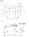
実施例1は、本発明の第1の態様に係る撮像装置及び撮像方法に関する。より具体的には、実施例1の撮像装置は、第1の構成、及び、第4Aの構成を有する。実施例1の撮像装置1の概念図を図1に示す。 Example 1 relates to an imaging apparatus and an imaging method according to the first aspect of the present invention. More specifically, the imaging apparatus according to the first embodiment has the first configuration and the fourth configuration. FIG. 1 shows a conceptual diagram of the image pickup apparatus 1 according to the first embodiment.
実施例1の撮像装置1は、撮像対象物を撮像して撮像データDoutを出力するものであり、
(A)撮像レンズ11、
(B)撮像レンズ11を通過した光が入射するマイクロレンズアレイ部12、及び、
(C)マイクロレンズアレイ部12から出射された光を受光する撮像素子(撮像手段)13、
を備えている。そして、マイクロレンズアレイ部12を構成する各マイクロレンズ12’は、印加される電圧に応じて焦点距離が可変である。
The imaging device 1 according to the first embodiment captures an imaging target and outputs imaging data Dout .
(A)
(B) a
(C) an imaging element (imaging means) 13 that receives light emitted from the
It has. And each micro lens 12 'which comprises the micro
ここで、実施例1の撮像装置1にあっては、
第1の撮像モード及び第2の撮像モードによって撮像がなされ、
第1の撮像モードによる撮像時、マイクロレンズアレイ部12を構成する各マイクロレンズ12’の焦点距離が無限大とされることで、撮像レンズ11による像が撮像素子13上に結像され(図1においては、点線の光線で示す)、
第2の撮像モードによる撮像時、撮像レンズ11による像がマイクロレンズ12’上に結像され、各マイクロレンズ12’の焦点距離が有限の値とされることで、マイクロレンズ12’上に結像された撮像レンズ11による像が撮像素子13上に投影される(図1においては、実線の光線で示す)。
Here, in the imaging apparatus 1 of the first embodiment,
Imaging is performed in the first imaging mode and the second imaging mode,
At the time of imaging in the first imaging mode, the focal length of each microlens 12 ′ constituting the
At the time of imaging in the second imaging mode, an image by the
また、実施例1の撮像装置1は、更に、
(D)撮像素子13からの信号に対して所定の画像処理を施すための画像処理部14、及び、
(E)マイクロレンズアレイ部12に電圧を印加するための電圧供給部(撮像モード切替部にも相当する)15、
を備え、
(F)画像処理部14及び電圧供給部15を制御する制御部17、
を更に備えている。
In addition, the imaging apparatus 1 according to the first embodiment further includes:
(D) an
(E) a voltage supply unit (which also corresponds to an imaging mode switching unit) 15 for applying a voltage to the
With
(F) a
Is further provided.
そして、撮像装置1においては、第1の撮像モード及び第2の撮像モードによって撮像がなされ、第1の撮像モードによる撮像時、電圧供給部15からマイクロレンズアレイ部12への電圧の印加が停止され、且つ、画像処理部14による所定の画像処理が停止され、第2の撮像モードによる撮像時、電圧供給部15からマイクロレンズアレイ部12への電圧の印加が行われ、且つ、画像処理部14による所定の画像処理が行われる。
In the imaging apparatus 1, imaging is performed in the first imaging mode and the second imaging mode, and application of voltage from the
実施例1、あるいは、後述する実施例2〜実施例4において、撮像レンズ11は、撮像対象物を撮像するためのメインレンズであり、例えば、ビデオカメラやスチルカメラ等で使用される一般的な撮像レンズから構成されている。また、マイクロレンズアレイ部12は、複数(実施例1にあっては、P×Q=325×230個)のマイクロレンズ12’が2次元マトリクス状に配列されて成り、撮像レンズ11の合焦点状態にも依るが、撮像レンズ11の焦点面に配置されている。尚、図中の符号f1は、撮像レンズ11の中心からマイクロレンズアレイ部12の結像面までの距離を表す。ここで、マイクロレンズアレイ部12は、液晶レンズアレイから構成されている。撮像素子13は、例えば、2次元マトリクス状に配列された複数のCCD(実施例1にあっては、画素数M×N=4032×2688個)から構成されている。撮像素子13においては、マイクロレンズアレイ部12から出射された光を受光して、撮像信号が生成される。撮像素子13は、マイクロレンズアレイ部12の焦点面に配置されている。尚、図中の符号f2は、マイクロレンズアレイ部12の中心から撮像素子13の撮像面までの距離(マイクロレンズ12’の焦点距離)を表し、例えば、f2=0.432mmである。撮像素子駆動手段16によって、撮像素子13が駆動され、撮像素子13の受光動作の制御が行われる。制御部17は、画像処理部14、電圧供給部15及び撮像素子駆動手段16の動作を制御する。具体的には、撮像素子駆動手段16の駆動動作を適宜制御すると共に、第1の撮像モード及び第2の撮像モードの2つの撮像モードに応じて、画像処理部14及び電圧供給部15の動作を制御する。制御部17は、マイクロコンピュータから構成されている。
In Embodiment 1 or Embodiments 2 to 4 to be described later, the
実施例1、あるいは、後述する実施例2〜実施例4において、電圧供給部15によって、マイクロレンズアレイ部12に電圧が印加される。そして、実施例1、あるいは、後述する実施例2〜実施例3にあっては、マイクロレンズアレイ部12への電圧の印加状態に応じて、2つの撮像モード、即ち、通常の高解像度での撮像モードである第1の撮像モード、及び、ライト・フィールド・フォトグラフィー技術に基づく撮像モードである第2の撮像モードの間の切り替えが行われる。
In Example 1 or Examples 2 to 4 described later, a voltage is applied to the
実施例1、あるいは、後述する実施例2〜実施例4において、第2の撮像モードにあっては、画像処理部14において所定の画像処理が施される。画像処理部14は、第2の撮像モードにおいて、撮像素子13で得られた信号(撮像信号)に対して所定の画像処理を施し、撮像データDoutとして出力する。具体的には、ライト・フィールド・フォトグラフィー技術に基づくリフォーカス(Refocusing)演算処理が行われる。そして、これによって、任意の視点や方向からの観察画像を再構築することができるし、画像の3次元情報を取得することができる。尚、リフォーカス演算処理については後述する。
In Example 1 or Examples 2 to 4 to be described later, in the second imaging mode, the
実施例1、あるいは、後述する実施例2におけるマイクロレンズアレイ部12の模式的な一部断面図を図2の(A)に示す。マイクロレンズアレイ部12は、液晶レンズアレイから構成されており、液晶レンズアレイは、
(a)第1電極22を有する第1基板21、
(b)第2電極24を有する第2基板25、及び、
(c)第1電極と第2電極との間に配置された液晶層23、
から構成されている。そして、第1電極22及び第2電極24への電圧の印加の有無によって、液晶レンズアレイがレンズとして機能する。ここで、第1電極22及び第2電極24の内の少なくとも一方の電極(実施例1にあっては第1電極22)は、マイクロレンズ12’を構成するための曲面を有している。尚、第1電極22、第2電極24には、電圧供給部15から電圧が印加される。また、第1電極22、第2電極24は共通電極(コモン電極)であり、それぞれが1枚の電極から構成されている。実施例1にあっては、撮像装置1の光軸をZ軸とした3次元ガウス空間を想定し、液晶レンズアレイがレンズとして機能するとき、各マイクロレンズ12’は、X軸方向及びY軸方向において略等しいパワー(光学パワー)を有している。具体的には、Z軸と直交する任意の軸を想定し、係る軸とZ軸とを含む仮想平面を想定したとき、最大パワーが得られる仮想平面に含まれる軸をX軸とし、X軸方向におけるパワーをPX、Y軸方向におけるパワーをPYとすると、例えば、PY=PXである。即ち、このような構成にあっては、液晶レンズアレイは、Z軸を中心として等方的な焦点距離を有するマイクロレンズアレイ部を構成する。尚、このような液晶レンズアレイとして、限定するものではないが、例えば、特開2006−18325や特開2006−189434に開示された光学特性可変光学素子を用いればよい。
FIG. 2A shows a schematic partial cross-sectional view of the
(A) a
(B) a
(C) a
It is composed of The liquid crystal lens array functions as a lens depending on whether or not voltage is applied to the
ここで、第1基板21及び第2基板25は、それぞれ、入射光を透過するガラス基板といった透明基板から構成されている。また、第1電極22及び第2電極24は、それぞれ、例えばITO(Indium TinOxide;酸化インジウムスズ)等の透明電極から構成されており、第1基板21及び第2基板25と同様に、入射光を透過する。第1電極22及び第2電極24の表面S1,S2の内、電極22側の表面S1には、上述したとおり、凹状の複数の曲面が2次元マトリクス状に形成されている。液晶層23は、無偏光・等方性屈折率液晶、例えばネマティック液晶から構成されており、第1電極22、第2電極24間に印加される電圧に応じて、液晶層23における液晶分子の配列状態が変わることで、屈折率が変化する。尚、このような液晶レンズアレイの基本的な構成、構造は、後述する実施例2〜実施例4における液晶レンズアレイから構成されたマイクロレンズアレイ部にあっても同様とすることができる。
Here, the
尚、実施例1の撮像装置1のように、様々な波長領域の光を含んだ自然光を撮像に利用する場合には、第1電極22側の表面S1を非球面とし、マイクロレンズ12’を非球面レンズとすることが好ましい。球面レンズで構成した場合と比べて、曲率を小さくことができる結果、光学設計が容易になる。また、マイクロレンズ12’を回折レンズで構成した場合と比較すると、入射光を屈折させる際の波長依存性が無くなるため、軸上色収差等の発生を回避することができ、様々な波長領域の光を含んだ自然光による撮像に適した構成とすることができる。尚、単色光を用いたイメージング用途等の場合には、波長依存性や軸上色収差の問題が無いため、マイクロレンズ12’を回折レンズで構成した方が、非球面レンズで構成した場合と比べて、優れた光学特性を得ることができる場合がある。
When natural light including light in various wavelength regions is used for imaging as in the imaging device 1 of the first embodiment, the surface S 1 on the
図1、図3の(A)及び(B)、図4の(A)及び(B)を参照して、実施例1の撮像装置1の動作について詳細に説明する。ここで、図3の(A)及び(B)は、マイクロレンズアレイ部12のレンズ効果を説明するための模式的な一部断面図であり、図3の(A)には、マイクロレンズアレイ部12に対して電圧を印加していない場合(第1の撮像モード)を示し、図3の(B)には、マイクロレンズアレイ部12に電圧を印加している場合(第2の撮像モード)を示す。
With reference to FIGS. 1 and 3A and 3B, and FIGS. 4A and 4B, the operation of the imaging apparatus 1 according to the first embodiment will be described in detail. Here, FIGS. 3A and 3B are schematic partial cross-sectional views for explaining the lens effect of the
実施例1の撮像装置1にあっては、第2の撮像モード時、撮像レンズ11による撮像対象物の像は、マイクロレンズ12’上に結像する。そして、マイクロレンズ12’から出射された光は、撮像素子13へ到達して、投影され、撮像素子駆動手段16の制御下、撮像素子13から撮像信号が得られる。即ち、電圧供給部15から第1電極22、第2電極24に電圧が印加される第2の撮像モードにあっては、液晶層23の屈折率が変化するため、図3の(B)に示すように、マイクロレンズ12’に入射した入射光L11は、マイクロレンズ12’において屈折され、光軸L0上の焦点である画素PL11に集光される。このように、第2の撮像モードによる撮像時、マイクロレンズアレイ部12への電圧の印加を行い、マイクロレンズアレイ部12を構成する各マイクロレンズ12’の焦点距離を有限な値とすることで(具体的には、マイクロレンズ12’の焦点距離を、マイクロレンズアレイ部12の結像面から撮像素子13の撮像面までの距離とすることで)、マイクロレンズ12’上に結像された撮像レンズ11による像を、撮像素子13上に投影(集光、収束)させることができる。
In the imaging apparatus 1 according to the first embodiment, in the second imaging mode, the image of the object to be imaged by the
一方、第1の撮像モード時、マイクロレンズアレイ部12を構成する各マイクロレンズ12’の焦点距離は無限大とされ、撮像レンズ11による撮像対象物の像は、マイクロレンズ12’によって何らの影響を受けること無く、撮像素子13上に結像する。そして、撮像素子駆動手段16の制御下、撮像素子13から撮像信号が得られる。即ち、電圧供給部15から第1電極22、第2電極24に電圧が印加されない第1の撮像モードにあっては、液晶層23の屈折率は変化しないため、図3の(A)に示すように、マイクロレンズアレイ部12に入射した光は、マイクロレンズ12’において屈折されない。マイクロレンズアレイ部12の焦点距離は無限大であり、撮像素子13に向かってそのまま進行する。このように、第1の撮像モードによる撮像時、マイクロレンズアレイ部12への電圧の印加を停止し、マイクロレンズアレイ部12を構成する各マイクロレンズ12’の焦点距離を無限大とすることで、撮像レンズ11による像を撮像素子13上に結像させることができる。
On the other hand, in the first imaging mode, the focal length of each microlens 12 ′ constituting the
このように、通常の高解像度の撮像モード(第1の撮像モード)にあっては、制御部17の制御下、電圧供給部15によるマイクロレンズアレイ部12への電圧の印加が停止される結果、マイクロレンズアレイ部12を構成する各マイクロレンズ12’の焦点距離が無限大となり、マイクロレンズアレイ部12への入射光がそのまま進行し、撮像レンズ11による像を撮像素子13上に結像させる。即ち、撮像レンズ11による像がそのまま撮像素子13へ到達し、通常の高解像度の撮像データが得られる。一方、ライト・フィールド・フォトグラフィー技術に基づく撮像モード(第2の撮像モード)にあっては、撮像レンズ11による像をマイクロレンズ12’上に結像させる。そして、制御部17の制御下、電圧供給部15によるマイクロレンズアレイ部12へ電圧が印加される結果、マイクロレンズ12’からの出射光が撮像素子13上に集光される。即ち、マイクロレンズアレイ部12を構成する各マイクロレンズ12’の焦点距離を有限な値とすることで、撮像レンズ11による像を撮像素子13上に投影させることができる。具体的には、図3の(B)に示すように、マイクロレンズアレイ部12への入射光L11(実線で示す)は、撮像素子13上の点(画素)PL11に投影され、マイクロレンズアレイ部12への入射光L12(点線で示す)は、撮像素子13上の点(画素)PL12に投影され、マイクロレンズアレイ部12への入射光L13(一点鎖線で示す)は、撮像素子13上の点(画素)PL13に投影される。即ち、マイクロレンズアレイ部12への入射光の入射方向が異なると、撮像素子13上の異なる点(異なる画素)上に投影(集光)される。
As described above, in the normal high-resolution imaging mode (first imaging mode), the
撮像素子13で得られた撮像信号は、画像処理部14へ送出される。そして、画像処理部14では、制御部17の制御下、この撮像信号に対して所定の画像処理が施され、撮像データDoutとして出力される。具体的には、第1の撮像モードにあっては、制御部17の制御下、画像処理部14による所定の画像処理を停止させる結果、入力した撮像信号がそのまま撮像データDoutとして出力される。一方、第2の撮像モードにあっては、制御部17の制御下、画像処理部14による所定の画像処理(リフォーカス演算処理)がなされる結果、入力した撮像信号に対して所定の画像処理が施され、撮像データDoutとして出力される。
An imaging signal obtained by the
ここで、図4の(A)及び(B)を参照して、画像処理部14における所定の画像処理であるリフォーカス演算処理について詳細に説明する。尚、このリフォーカス演算処理は、後述する実施例2〜実施例4に対しても同様に適用される。
Here, with reference to FIG. 4A and FIG. 4B, the refocus calculation process which is a predetermined image process in the
図4の(A)に示すように、撮像レンズ11の撮像レンズ面11A上において直交座標系(u,v)を想定し、撮像素子13の撮像面13A上において直交座標系(x,y)を想定する。撮像レンズ11の撮像レンズ面と撮像素子13の撮像面との間の距離をfとすると、図4の(A)に示すような撮像レンズ11及び撮像素子13を通る光線L14は、4次元関数LF(x,y,u,v)で表すことができる。従って、光線L14の位置情報に加え、光線L14の進行方向の情報を得ることができる。そして、この場合、図4の(B)に示すように撮像レンズ面11A、撮像面13A及びリフォーカス面(撮像レンズ11による像が結像されるマイクロレンズアレイ部12の結像面)12A間の位置関係を設定した場合、即ち、f’=α・fとなるようにリフォーカス面12Aを設定した場合、リフォーカス面12A上の座標(s,t)の撮像面13A上における検出光強度LF'(s,t,u,v)は、以下の式(1)で表すことができる。また、リフォーカス面12Aで得られるイメージEF'(s,t)は、検出光強度LF'(s,t,u,v)をレンズ口径に関して積分したものであるので、以下の式(2)で表すことができる。従って、式(2)に基づきリフォーカス演算を行うことによって、ライト・フィールド・フォトグラフィー技術に基づく撮像データDoutにより、任意の視点や方向からの観察画像を再構築することができるし、画像の3次元情報を取得することができる。
As shown in FIG. 4A, an orthogonal coordinate system (u, v) is assumed on the

このように、実施例1にあっては、マイクロレンズアレイ部12を液晶レンズアレイから構成したので、液晶層23に対する電圧の印加の有無に応じて液晶層23の屈折率を変化させ、入射光の屈折方向(焦点位置)を変化させることができる。即ち、電圧供給部15からマイクロレンズアレイ部12に電圧が印加されると、マイクロレンズアレイ部12を構成するマイクロレンズ12’への入射光が屈折され、撮像素子13上に投影される。一方、マイクロレンズアレイ部12に電圧が印加されていない状態では、入射光は屈折されず、そのままの状態で撮像素子13にて結像される。従って、入射光が撮像素子13上に投影されて得られた撮像信号に所定の画像処理を施す第2の撮像モードと、入射光をそのままの方向にて撮像素子13にて結像させて撮像信号を得る第1の撮像モードとの間で、撮像モードの切り替えが可能となる。また、第1の撮像モード及び第2の撮像モードにおいて、同じ撮像光学系(撮像レンズ11、マイクロレンズアレイ部12及び撮像素子13)を用いているので、装置構成が複雑になることはない。しかも、電気的に撮像モードを切り替えるので、機械的に切り替える場合と比較して、切り替え動作時の信頼性が向上する。
Thus, in Example 1, since the
更には、マイクロレンズ12’を非球面レンズから構成すれば、球面レンズから構成した場合と比較して、曲率を小さくことができるので、光学設計を容易にすることが可能となる。また、回折レンズで構成した場合と比較すると、入射光を屈折させる際の波長依存性を無くすことができ、軸上色収差等の発生を回避することができる。それ故、様々な波長領域の光を含んだ自然光を利用する撮像装置として最適な構成とすることが可能となる。
Furthermore, if the
尚、以上に説明した実施例1にあっては、場合によっては、第1の撮像モードによる撮像時、及び、第2の撮像モードによる撮像時の電圧供給部15からマイクロレンズアレイ部12への電圧の印加の状態を逆とした、第2の構成とすることもできる。即ち、
(D)撮像素子13からの信号に対して所定の画像処理を施すための画像処理部14、及び、
(E)マイクロレンズアレイ部12に電圧を印加するための電圧供給部15、
を更に備えており、
撮像装置においては、第1の撮像モード(通常撮像モード)及び第2の撮像モード(ライト・フィールド・フォトグラフィー技術に基づく撮像モード)によって撮像がなされ、
第1の撮像モードによる撮像時、電圧供給部15からマイクロレンズアレイ部12への電圧の印加が行われ、且つ、画像処理部14による所定の画像処理が停止され、
第2の撮像モードによる撮像時、電圧供給部15からマイクロレンズアレイ部12への電圧の印加が停止され、且つ、画像処理部14による所定の画像処理が行われる構成とすることもできる。尚、後述する実施例2〜実施例3においても同様とすることができる。
In the first embodiment described above, in some cases, the
(D) an
(E) a
Is further provided,
In the imaging apparatus, imaging is performed in the first imaging mode (normal imaging mode) and the second imaging mode (imaging mode based on light field photography technology),
During imaging in the first imaging mode, voltage application from the
During imaging in the second imaging mode, the application of voltage from the
実施例2は、実施例1の変形であり、具体的には、第3の構成、及び、第4Aの構成に関する。実施例2の撮像装置の概念図を図5に示すが、実施例2の撮像装置2にあっては、撮像レンズ11とマイクロレンズアレイ部12との間の距離を一定に保ちつつ、マイクロレンズアレイ部12と撮像素子(撮像手段)13との間の距離を変化させる駆動手段18が更に備えられている。そして、撮像レンズ11のFナンバーとマイクロレンズアレイ部12を構成するマイクロレンズのFナンバーとの間に不整合が生じた場合、電圧供給部15からマイクロレンズアレイ部12へ印加する電圧が変化させられると共に、駆動手段18によってマイクロレンズアレイ部12と撮像素子13との間の距離が変化させられる。駆動手段(撮像素子シフト部に相当する)18は、電気信号を機械的動作に変換させる素子、例えば、ピエゾ素子や、圧電アクチュエータ、バイメタルから構成することができる。
The second embodiment is a modification of the first embodiment, and specifically relates to the third configuration and the fourth configuration. FIG. 5 shows a conceptual diagram of the image pickup apparatus of the second embodiment. In the image pickup apparatus 2 of the second embodiment, the microlens is maintained while keeping the distance between the
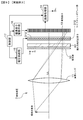
図5、図6、及び、図7の(A)〜(D)を参照して、実施例2の撮像装置2における特徴的な動作である、Fナンバーの整合処理(撮像レンズ11の絞り値を変更する際の撮像光学系の最適化処理)について詳細に説明する。ここで、図6は、絞り値変更の際の撮像光学系の最適化処理を流れ図で表したものであり、図7の(A)〜(D)は、撮像レンズ11の絞り値を変更する際の撮像光学系の最適化処理における光路の一例を説明するための撮像レンズ11等の模式的な模式図である。尚、撮像装置2の基本動作(撮像動作)は、実施例1の撮像装置1と同様とすることができるので、詳細な説明は省略する。
With reference to FIGS. 5, 6, and 7 (A) to 7 (D), F number matching processing (aperture value of the imaging lens 11), which is a characteristic operation in the imaging apparatus 2 of the second embodiment. (Optimization processing of the imaging optical system when changing the above) will be described in detail. Here, FIG. 6 is a flowchart showing optimization processing of the imaging optical system when changing the aperture value. FIGS. 7A to 7D change the aperture value of the
撮像装置2では、例えば図7の(A)に示す光線L21,L22のように、撮像レンズ11のFナンバーとマイクロレンズアレイ部12を構成するマイクロレンズのFナンバー(以下、単に、マイクロレンズのFナンバーと呼ぶ)とが整合している場合を、先ず、想定する。そして、図7の(A)に示した状態から、撮像レンズ11の絞り値が変更された場合には(図6のステップ−S21)、図7の(B)に示す光線L23,L22のように、撮像レンズ11の(入射瞳径11’からの)Fナンバーと、マイクロレンズのFナンバーとの間で不整合が生じる(ステップ−S22)。図7の(B)に示した例の場合には、制御部17によって、電圧供給部15からマイクロレンズアレイ部12に印加される電圧を変化させ、マイクロレンズアレイ部12において発生するパワーを変化させる(ステップ−S23)。
In the imaging device 2, for example, like the light beams L 21 and L 22 shown in FIG. 7A, the F number of the
すると、図7の(C)に示すように、マイクロレンズアレイ部12での光の屈折が緩和され、マイクロレンズアレイ部12から射出する光が、光線L22から光線L24のように変化する。すると、光線L23,L24に示すように、撮像レンズ11の(入射瞳径11’からの)Fナンバーと、マイクロレンズのFナンバーとが再び整合するようになる(ステップ−S24)。但し、図7の(C)から分かるように、図7の(A)及び(B)における光線L22の場合とは異なり、撮像素子13において1つのマイクロレンズに対応する撮像領域13’(図7の(A)〜(D)においては、斜線を付した領域で示す)と、この撮像領域13’上における光線L24の到達領域とが一致しなくなり、このままでは、撮像の際の解像度が低下してしまう。
Then, as shown in FIG. 7 (C), is alleviated refraction of light by the
そこで、次に、制御部17によって駆動手段(撮像素子シフト部)18を制御し、撮像素子13を、光軸L0(撮像装置の光軸LL)に沿って、図示した例では、マイクロレンズアレイ部12から離れる方向に移動させる(ステップ−S25)。すると、図7の(D)に示した光線L23,L24のように、撮像領域13’と、この撮像領域13’における光線L24の到達領域とが再び一致するようになり、撮像素子13での撮像領域が最適化される。このようにして、撮像レンズ11の絞り値を変更する際の撮像光学系の最適化処理が終了する。実施例2にあっては、このような処理を行うので、撮像の際の解像度低下が生じない。駆動手段18を、例えば電気信号を機械的動作に変換させる素子から構成すれば、簡易、且つ、省スペースな構成とすることができる。
Therefore, next, the
尚、マイクロレンズアレイ部12を構成するマイクロレンズのパワー変更処理(ステップ−S23)を行った後に、撮像素子13のシフト処理(ステップ−S25)を行う代わりに、撮像素子13のシフト処理(ステップ−S25)を行った後に、マイクロレンズアレイ部12を構成するマイクロレンズのパワー変更処理(ステップ−S23)を行ってもよい。
In addition, after performing the power change process (step-S23) of the microlens which comprises the
また、撮像レンズ11とマイクロレンズのFナンバーを整合させた後に、駆動手段18が撮像素子13を移動させることで、マイクロレンズアレイ部12と撮像素子13との間の距離を変化させたが、代替的に、ステップ−S21〜S−24の処理後に、図7の(D)を参照して説明した動作の代わりに、図8の(A)及び(B)に示すように、駆動手段によって、撮像レンズ11とマイクロレンズアレイ部12との間の距離を一定に保ちつつ、撮像レンズ11及びマイクロレンズアレイ部12を撮像装置の光軸LLに沿って移動させる構成とすることもできる。具体的には、撮像素子13上での像の大きさが、光線L21,L22による場合と、移動後の光線L23,L24による場合とで一致するように(撮像領域が共に撮像領域13’となるように)、撮像レンズ11及びマイクロレンズアレイ部12を撮像装置の光軸L0(撮像装置の光軸LL)に沿って移動させる。撮像レンズ11を移動させる機構としては、通常の撮像に用いる際の撮像レンズの駆動機構を利用すればよい。
In addition, after the F number of the
以上の実施例2において説明した駆動手段18、及び、Fナンバーの整合処理(撮像レンズの絞り値を変更する際の撮像光学系の最適化処理)を、後述する実施例3〜実施例4にも適用することができる。 The driving means 18 and F-number matching processing (processing for optimizing the imaging optical system when changing the aperture value of the imaging lens) described in the second embodiment is applied to the third to fourth embodiments described later. Can also be applied.
実施例3も、実施例1の変形である。実施例3にあっては第4Bの構成を採用した。即ち、図9に概念図を示すように、撮像装置3の光軸をZ軸とした3次元ガウス空間を想定したとき、撮像レンズ11とマイクロレンズアレイ部312との間には、X軸方向に偏光した光を出射する偏光板30、及び、偏光方向可変素子40が、配置されている。そして、マイクロレンズアレイ部312を構成する液晶レンズアレイがレンズとして機能するとき、各マイクロレンズは、X軸方向にはパワー(光学パワー)を有さず、Y軸方向にはパワー(光学パワー)を有する。即ち、液晶レンズアレイは、Z軸を中心として異方的な焦点距離を有するマイクロレンズアレイ部312を構成する。云い換えれば、液晶レンズアレイを構成する各液晶レンズは、YZ平面内において有限の焦点距離を有し、XZ平面内において無限大の焦点距離を有するマイクロレンズを構成する。
The third embodiment is also a modification of the first embodiment. In Example 3, the configuration of 4B was adopted. That is, as shown in a conceptual diagram in FIG. 9, when assuming a three-dimensional Gaussian space in which the optical axis of the imaging device 3 is the Z axis, there is an X-axis direction between the
偏光方向可変素子40は液晶素子から成る。具体的には、偏光方向可変素子40は、図2の(B)に模式的な一部断面図を示すように、
(a’)一対の基板41,45、
(b’)一対の基板41,45のそれぞれに設けられた電極42,44、及び、
(c’)一対の基板41,45のそれぞれに設けられた電極42,44の間に配置された液晶層43、
から構成されている。ここで、一方の基板41近傍における液晶分子の配向方向はX軸方向と平行であり、他方の基板45近傍における液晶分子の配向方向はY軸方向と平行である。また、電極42は平坦な1枚の電極から構成され、電極44も平坦な1枚の電極から構成されている。
The polarization direction
(A ′) a pair of
(B ′) electrodes 42 and 44 provided on each of the pair of
(C ′) a
It is composed of Here, the alignment direction of the liquid crystal molecules in the vicinity of one
実施例3にあっては、光源として、限定するものではないが、単色光の光源を使用する。偏光板30を通過した光は、X軸に平行な偏光成分のみを有する。そして、偏光方向可変素子40の第1の動作モードにあっては、偏光方向可変素子40を通過した光は、偏光方向可変素子40を構成する液晶分子によって偏光方向を曲げられず、元の方向のままである。マイクロレンズアレイ部312を構成する液晶レンズアレイを構成する各液晶レンズは、Z軸を中心として異方的な焦点距離を有するマイクロレンズ(X軸方向の焦点距離は無限大であり、Y軸方向の焦点距離は有限の値)であるが故に、マイクロレンズ312’を通過した光(撮像レンズ11による像)は、マイクロレンズ312’によって変化を受けることがない。そして、マイクロレンズ312’を通過した光(撮像レンズ11による像)は、撮像素子(撮像手段)13において結像する。この状態を、模式的に、図10の(A)に示す。
In the third embodiment, the light source is not limited, but a monochromatic light source is used. The light that has passed through the
一方、偏光方向可変素子40の第2の動作モードにあっては、偏光方向可変素子40を通過した光は、偏光方向可変素子40を構成する液晶分子によって偏光方向をY軸方向に曲げられる。ここで、上述したとおり、マイクロレンズアレイ部312を構成する液晶レンズアレイにおける各液晶レンズは、Z軸を中心として異方的な焦点距離を有するマイクロレンズ(X軸方向の焦点距離は無限大であり、Y軸方向の焦点距離は有限の値)であるが故に、マイクロレンズ312’において結像した光(撮像レンズ11による像)は、撮像素子13上に投影される。
On the other hand, in the second operation mode of the polarization direction
そして、実施例3にあっては、偏光方向可変素子40を第1の動作モードとしたとき、第1の撮像モードとし、偏光方向可変素子40を第2の動作モードとしたとき、第2の撮像モードとすればよい。
In the third embodiment, when the polarization direction
このような液晶レンズアレイとして、限定するものではないが、例えば、特開2006−079669に開示された液晶レンズ素子や、特開平5−034656に開示された焦点距離可変液晶レンズを用いればよい。これらの液晶レンズ素子あるいは液晶レンズは、ラビング方向と同方向の偏光方向の光のみに対してレンズ効果を発現する。従って、一対の基板41,45におけるラビング方向を、X軸方向と平行な方向、及び、Y軸方向と平行な方向とすればよい。
Although not limited as such a liquid crystal lens array, for example, a liquid crystal lens element disclosed in Japanese Patent Application Laid-Open No. 2006-079669 or a variable focal length liquid crystal lens disclosed in Japanese Patent Application Laid-Open No. 5-034656 may be used. These liquid crystal lens elements or liquid crystal lenses exhibit a lens effect only for light having a polarization direction that is the same as the rubbing direction. Therefore, the rubbing direction in the pair of
使用する液晶層43を構成する液晶材料の種類によって、電極42,44に電圧を印加したときに、第2の動作モードを得る場合もあるし、電極42,44に電圧を印加しないときに、第2の動作モードを得る場合もある。また、液晶層43を構成する液晶材料の種類によっては、液晶レンズアレイがレンズとして機能するとき、各マイクロレンズは、Y軸方向にはパワー(光学パワー)を有さず(この状態を、模式的に、図11の(A)に示す)、X軸方向にはパワー(光学パワー)を有する(この状態を、模式的に、図11の(B)に示す)構成、即ち、第4Cの構成とすることもできる。このような第4Cの構成にあっては、液晶レンズアレイは、Z軸を中心として異方的な焦点距離を有するマイクロレンズアレイ部312を構成する。即ち、液晶レンズアレイを構成する各液晶レンズは、XZ平面内において有限の焦点距離を有し、YZ平面内において無限大の焦点距離を有するマイクロレンズを構成する。そして、この場合にも、電極42,44に電圧を印加したときに、第2の動作モードを得る場合もあるし、電極42,44に電圧を印加しないときに、第2の動作モードを得る場合もある。後述する実施例4においても同様である。
Depending on the type of liquid crystal material constituting the
実施例3の撮像装置3、あるいは又、後述する実施例4の撮像装置4のように、単色光を撮像に利用する場合には、マイクロレンズを回折レンズで構成した方が、波長依存性や軸上色収差の問題が無いため、非球面レンズで構成した場合と比べて、優れた光学特性を得ることができる。 When the monochromatic light is used for imaging as in the imaging device 3 of the third embodiment or the imaging device 4 of the fourth embodiment which will be described later, it is more preferable to configure the microlens with a diffraction lens. Since there is no problem of axial chromatic aberration, superior optical characteristics can be obtained as compared with the case of an aspheric lens.
実施例4は、本発明の第2の態様に係る撮像装置及び撮像方法に関する。実施例4の撮像装置4の概念図を、図12に示す。即ち、実施例4の撮像装置4は、実施例3における撮像装置3と同様に、
(A)撮像レンズ11、
(B)撮像レンズ11を通過した光が入射するマイクロレンズアレイ部412、及び、
(C)マイクロレンズアレイ部412から出射された光を受光する撮像素子(撮像手段)13、
を備えており、撮像装置4の光軸をZ軸とした3次元ガウス空間を想定したとき、撮像レンズ11とマイクロレンズアレイ部412との間には、X軸方向に偏光した光を出射する偏光板30、及び、偏光方向可変素子40が、更に配置されている。
Example 4 relates to an imaging apparatus and an imaging method according to the second aspect of the present invention. FIG. 12 shows a conceptual diagram of the image pickup apparatus 4 of the fourth embodiment. That is, the imaging device 4 of Example 4 is similar to the imaging device 3 of Example 3,
(A)
(B) a
(C) an imaging element (imaging means) 13 that receives light emitted from the
Assuming a three-dimensional Gaussian space in which the optical axis of the imaging device 4 is the Z axis, light polarized in the X-axis direction is emitted between the
そして、実施例3の撮像装置3と同様に、マイクロレンズアレイ部412は、液晶レンズアレイから構成されており、実施例4にあっては、マイクロレンズアレイ部412を構成する各マイクロレンズ412’は、X軸方向にはパワーを有さず、Y軸方向にはパワーを有している。実施例4にあっても、光源として、限定するものではないが、単色光の光源を使用する。
Similarly to the imaging device 3 of the third embodiment, the
実施例4の撮像装置4にあっては、実施例3の撮像装置3と同様に、
第1の撮像モード及び第2の撮像モードによって撮像がなされ、
第1の撮像モードによる撮像時、偏光方向可変素子40の作動によって、マイクロレンズアレイ部412を構成する各マイクロレンズ412’のパワーを有さない方向に偏光された光がマイクロレンズ412’を通過し、撮像レンズ11による像が撮像素子13上に結像され、
第2の撮像モードによる撮像時、偏光方向可変素子40の作動によって、マイクロレンズアレイ部412を構成する各マイクロレンズ412’のパワーを有する方向に偏光された光がマイクロレンズ412’に入射され、撮像レンズ11による像がマイクロレンズ412’上に結像され、マイクロレンズ412’上に結像された撮像レンズ11による像はマイクロレンズ412’によって撮像素子13に投影される。
In the imaging device 4 of the fourth embodiment, similarly to the imaging device 3 of the third embodiment,
Imaging is performed in the first imaging mode and the second imaging mode,
During imaging in the first imaging mode, the light polarized in the direction not having the power of each
During imaging in the second imaging mode, by the operation of the polarization direction
また、実施例4の撮像装置4においては、撮像素子13からの信号に対して所定の画像処理を施すための画像処理部14を更に備えている。そして、撮像装置4においては、第1の撮像モード及び第2の撮像モードによって撮像がなされ、第1の撮像モードによる撮像時、画像処理部14による所定の画像処理が停止され、第2の撮像モードによる撮像時、画像処理部14による所定の画像処理が行われる。
In addition, the imaging apparatus 4 according to the fourth embodiment further includes an
偏光方向可変素子40は、液晶素子から構成されている。偏光方向可変素子40を構成する液晶素子は、具体的には、実施例3において説明した液晶素子と同様とすることができるので、詳細な説明は省略する。また、実施例4の撮像装置4を構成する撮像レンズ11、マイクロレンズアレイ部412、及び、撮像素子13の構成、構造も、実施例3の撮像装置3を構成する撮像レンズ11、マイクロレンズアレイ部312、及び、撮像素子13の構成、構造と同様とすることができるので、詳細な説明は省略する。
The polarization direction
但し、実施例4の撮像装置4にあっては、第1の撮像モードと第2の撮像モードとの切り替えにあっては、電圧供給部15からのマイクロレンズアレイ部412への電圧の印加の有無で行うのではなく、上述したとおり、電圧供給部15からの偏光方向可変素子40を構成する電極42,44への電圧の印加の有無によって行われる。マイクロレンズアレイ部412にあっては、液晶層を構成する液晶材料に依存するが、マイクロレンズアレイ部412を構成する各マイクロレンズ412’が、X軸方向にはパワーを有さず、Y軸方向にはパワーを有する状態が達成できるように、マイクロレンズアレイ部412を構成する液晶レンズアレイの第1電極22、第2電極24に適切な電圧を印加すればよい。尚、実施例3において説明したと同様に、Y軸方向にはパワーを有さず、X軸方向にはパワーを有する状態が達成できるように、マイクロレンズアレイ部412を構成する液晶レンズアレイの第1電極22、第2電極24に適切な電圧を印加してもよい。通常、電圧供給部15からマイクロレンズアレイ部412へは、一定の値の電圧を印加すればよい。そして、実施例2において説明したように、Fナンバーの整合処理(撮像レンズ11の絞り値を変更する際の撮像光学系の最適化処理)を行う場合には、電圧供給部15からマイクロレンズアレイ部412への印加電圧の値を適切に変化させればよい。
However, in the imaging device 4 of the fourth embodiment, in switching between the first imaging mode and the second imaging mode, voltage application from the
以上、本発明を好ましい実施例に基づき説明したが、本発明はこれらの実施例に限定するものではなく、種々の変形が可能である。 As mentioned above, although this invention was demonstrated based on the preferable Example, this invention is not limited to these Examples, A various deformation | transformation is possible.
実施例1〜実施例4にあっては、マイクロレンズアレイ部において、電極22,24の表面S1,S2の内、表面S1が曲面である平凸レンズとしたが、代替的に、表面S2を曲面としてもよいし、表面S1,S2の両方が曲面である両凸レンズとしてもよい。実施例1〜実施例2にあっては、マイクロレンズアレイ部を、液晶レンズアレイから構成する代わりに、エレクトロウェッティング現象(電気毛管現象)を利用した液体マイクロレンズアレイ部を用いることもできる。更には、実施例にあっては、画像処理部14における所定の画像処理方法として、ライト・フィールド・フォトグラフィー技術に基づくリフォーカス演算処理について説明したが、画像処理部14における画像処理方法は、これに限られず、他の画像処理方法(例えば、視野を振るといった画像処理や、マイクロレンズアレイ部及び撮像素子を一種のステレオ・カメラとして機能させることで得られる距離算出といった画像処理)としてもよい。また、マイクロレンズアレイ部を構成する各レンズの形状は、円形に限定されず、矩形や六角形等の各種の多角形とすることもできる。矩形や六角形のレンズを用いることで、光利用効率が高められると共に、矩形や六角形のレンズが密に配列されたマイクロレンズアレイ部にあっては、円形のレンズにおけるレンズとレンズの間の平らな部分が存在しないので、円形のレンズにおけるレンズとレンズの間の平らな部分を通ってきた光線の影響を回避できるという利点がある。
In Example 1 to Example 4, in the microlens array portion, of the surface S 1, S 2 of the
1,2,3,4・・・撮像装置、11・・・撮像レンズ、11’・・・入射瞳径、11A・・・撮像レンズ面、12,312,412・・・マイクロレンズアレイ部、12’,312’412’・・・マイクロレンズ、12A・・・リフォーカス面、13・・・撮像素子、13A・・・撮像面、14・・・画像処理部、15・・・電圧供給部(撮像モード切替部)、16・・・撮像素子駆動手段、17・・・制御部、18・・・駆動手段(撮像素子シフト部)、21,25,41,45・・・基板、22,24,42,44・・・電極、23,43・・・液晶層 1, 2, 3, 4 ... imaging device, 11 ... imaging lens, 11 '... entrance pupil diameter, 11A ... imaging lens surface, 12, 312, 412 ... micro lens array section, 12 ′, 312′412 ′... Micro lens, 12A... Refocus plane, 13... Imaging element, 13A... Imaging plane, 14. (Imaging mode switching unit), 16... Imaging device driving means, 17... Control unit, 18... Driving means (imaging device shifting unit), 21, 25, 41, 45. 24, 42, 44 ... electrodes, 23, 43 ... liquid crystal layer
Claims (20)
(B)撮像レンズを通過した光が入射するマイクロレンズアレイ部、
(C)マイクロレンズアレイ部から出射された光を受光する撮像素子、
(D)撮像素子からの信号に対して所定の画像処理を施すための画像処理部、
(E)マイクロレンズアレイ部に電圧を印加するための電圧供給部、及び、
(F)撮像レンズとマイクロレンズアレイ部との間の距離を一定に保ちつつ、マイクロレンズアレイ部と撮像素子との間の距離を変化させる駆動手段、
を備えており、
マイクロレンズアレイ部を構成する各マイクロレンズは、印加される電圧に応じて焦点距離が可変であり、
撮像レンズのFナンバーとマイクロレンズアレイ部を構成するマイクロレンズのFナンバーとの間に不整合が生じた場合、電圧供給部からマイクロレンズアレイ部へ印加する電圧が変化させられると共に、駆動手段によってマイクロレンズアレイ部と撮像素子との間の距離が変化させられる撮像装置。 (A) an imaging lens,
(B) a microlens array unit on which light that has passed through the imaging lens is incident ;
(C) an image sensor that receives light emitted from the microlens array unit;
(D) an image processing unit for performing predetermined image processing on a signal from the image sensor;
(E) a voltage supply unit for applying a voltage to the microlens array unit, and
(F) Driving means for changing the distance between the microlens array unit and the imaging element while keeping the distance between the imaging lens and the microlens array unit constant;
With
Each micro lens forming the micro lens array unit, Ri variable focal length Der according to an applied voltage,
When a mismatch occurs between the F number of the imaging lens and the F number of the microlens array unit, the voltage applied from the voltage supply unit to the microlens array unit is changed, and the driving means An imaging apparatus in which a distance between a microlens array unit and an imaging element can be changed .
第1の撮像モードによる撮像時、マイクロレンズアレイ部を構成する各マイクロレンズの焦点距離が無限大とされることで、撮像レンズによる像が撮像素子上に結像され、
第2の撮像モードによる撮像時、撮像レンズによる像がマイクロレンズ上に結像され、各マイクロレンズの焦点距離が有限の値とされることで、マイクロレンズ上に結像された撮像レンズによる像が撮像素子上に投影される請求項1に記載の撮像装置。 Imaging is performed in the first imaging mode and the second imaging mode,
At the time of imaging in the first imaging mode, the focal length of each microlens constituting the microlens array unit is infinite, so that an image by the imaging lens is formed on the imaging element,
At the time of imaging in the second imaging mode, an image by the imaging lens is formed on the microlens, and the focal length of each microlens is set to a finite value so that the image by the imaging lens imaged on the microlens. The imaging apparatus according to claim 1, wherein is projected onto the imaging element.
第1の撮像モードによる撮像時、電圧供給部からマイクロレンズアレイ部への電圧の印加が停止され、且つ、画像処理部による所定の画像処理が停止され、
第2の撮像モードによる撮像時、電圧供給部からマイクロレンズアレイ部への電圧の印加が行われ、且つ、画像処理部による所定の画像処理が行われる請求項1に記載の撮像装置。 Imaging is performed in the first imaging mode and the second imaging mode,
During imaging in the first imaging mode, application of voltage from the voltage supply unit to the microlens array unit is stopped, and predetermined image processing by the image processing unit is stopped,
The imaging apparatus according to claim 1, wherein during imaging in the second imaging mode, voltage is applied from the voltage supply unit to the microlens array unit, and predetermined image processing is performed by the image processing unit.
第1の撮像モードによる撮像時、電圧供給部からマイクロレンズアレイ部への電圧の印加が行われ、且つ、画像処理部による所定の画像処理が停止され、
第2の撮像モードによる撮像時、電圧供給部からマイクロレンズアレイ部への電圧の印加が停止され、且つ、画像処理部による所定の画像処理が行われる請求項1に記載の撮像装置。 Imaging is performed in the first imaging mode and the second imaging mode,
During imaging in the first imaging mode, voltage is applied from the voltage supply unit to the microlens array unit, and predetermined image processing by the image processing unit is stopped,
The imaging apparatus according to claim 1, wherein during imaging in the second imaging mode, application of a voltage from the voltage supply unit to the microlens array unit is stopped, and predetermined image processing is performed by the image processing unit.
(a)第1電極を有する第1基板、
(b)第2電極を有する第2基板、及び、
(c)第1電極と第2電極との間に配置された液晶層、
から構成されており、
第1電極及び第2電極への電圧の印加の有無によって、液晶レンズアレイがレンズとして機能する請求項7に記載の撮像装置。 The liquid crystal lens array
(A) a first substrate having a first electrode;
(B) a second substrate having a second electrode, and
(C) a liquid crystal layer disposed between the first electrode and the second electrode;
Consists of
The imaging apparatus according to claim 7 , wherein the liquid crystal lens array functions as a lens depending on whether a voltage is applied to the first electrode and the second electrode.
液晶レンズアレイがレンズとして機能するとき、各マイクロレンズは、X軸方向にはパワーを有さず、Y軸方向にはパワーを有する請求項7に記載の撮像装置。 Assuming a three-dimensional Gaussian space where the optical axis of the imaging device is the Z-axis, a polarizing plate that emits light polarized in the X-axis direction and a variable polarization direction between the imaging lens and the microlens array unit The elements are arranged,
The imaging apparatus according to claim 7 , wherein when the liquid crystal lens array functions as a lens, each microlens has no power in the X-axis direction and has power in the Y-axis direction.
液晶レンズアレイがレンズとして機能するとき、各マイクロレンズは、Y軸方向にはパワーを有さず、X軸方向にはパワーを有する請求項7に記載の撮像装置。 Assuming a three-dimensional Gaussian space where the optical axis of the imaging device is the Z-axis, a polarizing plate that emits light polarized in the X-axis direction and a variable polarization direction between the imaging lens and the microlens array unit The elements are arranged,
The imaging device according to claim 7 , wherein when the liquid crystal lens array functions as a lens, each microlens has no power in the Y-axis direction and has power in the X-axis direction.
(B)撮像レンズを通過した光が入射するマイクロレンズアレイ部、
(C)マイクロレンズアレイ部から出射された光を受光する撮像素子、
(D)撮像素子からの信号に対して所定の画像処理を施すための画像処理部、及び、
(E)撮像レンズとマイクロレンズアレイ部との間の距離を一定に保ちつつ、マイクロレンズアレイ部と撮像素子との間の距離を変化させる駆動手段、
を備えた撮像装置であって、
撮像装置の光軸をZ軸とした3次元ガウス空間を想定したとき、撮像レンズとマイクロレンズアレイ部との間には、X軸方向に偏光した光を出射する偏光板、及び、偏光方向可変素子が、更に配置されており、
マイクロレンズアレイ部は、液晶レンズアレイから構成されており、
マイクロレンズアレイ部を構成する各マイクロレンズは、X軸方向にはパワーを有さず、Y軸方向にはパワーを有しており、あるいは又、Y軸方向にはパワーを有さず、X軸方向にはパワーを有しており、
撮像レンズのFナンバーとマイクロレンズアレイ部を構成するマイクロレンズのFナンバーとの間に不整合が生じた場合、マイクロレンズアレイ部を構成する各マイクロレンズのパワーが変化させられると共に、駆動手段によってマイクロレンズアレイ部と撮像素子との間の距離が変化させられる撮像装置。 (A) an imaging lens,
(B) a microlens array unit on which light that has passed through the imaging lens is incident ;
(C) an image sensor that receives light emitted from the microlens array unit;
(D) an image processing unit for performing predetermined image processing on a signal from the image sensor, and
(E) Driving means for changing the distance between the microlens array unit and the imaging element while keeping the distance between the imaging lens and the microlens array unit constant;
An imaging device comprising:
Assuming a three-dimensional Gaussian space where the optical axis of the imaging device is the Z-axis, a polarizing plate that emits light polarized in the X-axis direction and a variable polarization direction between the imaging lens and the microlens array unit An element is further arranged;
The micro lens array part is composed of a liquid crystal lens array,
Each microlens constituting the microlens array unit has no power in the X-axis direction, has power in the Y-axis direction, or has no power in the Y-axis direction. It has power in the axial direction ,
When a mismatch occurs between the F-number of the imaging lens and the F-number of the microlens array unit, the power of each microlens that configures the microlens array unit is changed, and the driving means An imaging apparatus in which a distance between a microlens array unit and an imaging element can be changed .
第1の撮像モードによる撮像時、偏光方向可変素子の作動によって、マイクロレンズアレイ部を構成する各マイクロレンズのパワーを有さない方向に偏光された光がマイクロレンズを通過し、撮像レンズによる像が撮像素子上に結像され、
第2の撮像モードによる撮像時、偏光方向可変素子の作動によって、マイクロレンズアレイ部を構成する各マイクロレンズのパワーを有する方向に偏光された光がマイクロレンズに入射され、撮像レンズによる像がマイクロレンズ上に結像され、マイクロレンズ上に結像された撮像レンズによる像がマイクロレンズによって撮像素子に投影される請求項13に記載の撮像装置。 Imaging is performed in the first imaging mode and the second imaging mode,
During imaging in the first imaging mode, the light polarized in the direction not having the power of each microlens constituting the microlens array unit passes through the microlens by the operation of the polarization direction variable element, and is imaged by the imaging lens. Is imaged on the image sensor,
During imaging in the second imaging mode, light polarized in a direction having the power of each microlens constituting the microlens array unit is incident on the microlens by the operation of the polarization direction variable element, and the image by the imaging lens is microscopically. The image pickup apparatus according to claim 13, wherein the image is formed on the lens and an image of the image pickup lens formed on the microlens is projected onto the image pickup element by the microlens.
第1の撮像モードによる撮像時、画像処理部による所定の画像処理が停止され、
第2の撮像モードによる撮像時、画像処理部による所定の画像処理が行われる請求項13に記載の撮像装置。 Imaging is performed in the first imaging mode and the second imaging mode,
During imaging in the first imaging mode, predetermined image processing by the image processing unit is stopped,
The imaging apparatus according to claim 13 , wherein predetermined image processing is performed by the image processing unit during imaging in the second imaging mode.
(B)撮像レンズを通過した光が入射するマイクロレンズアレイ部、及び、
(C)マイクロレンズアレイ部から出射された光を受光する撮像素子、
を備えており、
マイクロレンズアレイ部を構成する各マイクロレンズは、印加される電圧に応じて焦点距離が可変である撮像装置を用いた撮像方法であって、
第1の撮像モード及び第2の撮像モードによって撮像され、
第1の撮像モードによる撮像時、マイクロレンズアレイ部を構成する各マイクロレンズの焦点距離を無限大とすることで、撮像レンズによる像を撮像素子上に結像させ、
第2の撮像モードによる撮像時、撮像レンズによる像をマイクロレンズ上に結像させ、各マイクロレンズの焦点距離を有限の値とすることで、マイクロレンズ上に結像された撮像レンズによる像を撮像素子上に投影し、
撮像レンズのFナンバーとマイクロレンズアレイ部を構成するマイクロレンズのFナンバーとの間に不整合が生じた場合、マイクロレンズアレイ部を構成する各マイクロレンズのパワーを変化させると共に、撮像レンズとマイクロレンズアレイ部との間の距離を一定に保ちつつ、マイクロレンズアレイ部と撮像素子との間の距離を変化させる撮像方法。 (A) an imaging lens,
(B) a microlens array unit on which light that has passed through the imaging lens enters, and
(C) an image sensor that receives light emitted from the microlens array unit;
With
Each microlens constituting the microlens array unit is an imaging method using an imaging device whose focal length is variable according to an applied voltage,
Images are captured in the first imaging mode and the second imaging mode,
At the time of imaging in the first imaging mode, by making the focal length of each microlens constituting the microlens array unit infinite, an image by the imaging lens is formed on the imaging element,
At the time of imaging in the second imaging mode, an image by the imaging lens is formed on the microlens, and the focal length of each microlens is set to a finite value so that an image by the imaging lens imaged on the microlens is obtained. Project onto the image sensor ,
When a mismatch occurs between the F number of the imaging lens and the F number of the microlens array unit, the power of each microlens configuring the microlens array unit is changed, and the imaging lens and the microlens An imaging method for changing a distance between a microlens array part and an imaging element while keeping a distance between the lens array part constant .
(B)撮像レンズを通過した光が入射するマイクロレンズアレイ部、及び、
(C)マイクロレンズアレイ部から出射された光を受光する撮像素子、
を備えた撮像装置であって、
撮像装置の光軸をZ軸とした3次元ガウス空間を想定したとき、撮像レンズとマイクロレンズアレイ部との間には、X軸方向に偏光した光を出射する偏光板、及び、偏光方向可変素子が、更に配置されており、
マイクロレンズアレイ部は液晶レンズアレイから構成されており、
マイクロレンズアレイ部を構成する各マイクロレンズは、X軸方向にはパワーを有さず、Y軸方向にはパワーを有しており、あるいは又、Y軸方向にはパワーを有さず、X軸方向にはパワーを有している撮像装置を用いた撮像方法であって、
第1の撮像モード及び第2の撮像モードによって撮像され、
第1の撮像モードによる撮像時、偏光方向可変素子の作動によって、マイクロレンズアレイ部を構成する各マイクロレンズのパワーを有さない方向に偏光した光をマイクロレンズを通過させ、撮像レンズによる像を撮像素子上に結像させ、
第2の撮像モードによる撮像時、偏光方向可変素子の作動によって、マイクロレンズアレイ部を構成する各マイクロレンズのパワーを有する方向に偏光された光をマイクロレンズに入射させ、撮像レンズによる像をマイクロレンズ上に結像させ、マイクロレンズ上に結像された撮像レンズによる像をマイクロレンズによって撮像素子に投影し、
撮像レンズのFナンバーとマイクロレンズアレイ部を構成するマイクロレンズのFナンバーとの間に不整合が生じた場合、マイクロレンズアレイ部を構成する各マイクロレンズのパワーを変化させると共に、撮像レンズとマイクロレンズアレイ部との間の距離を一定に保ちつつ、マイクロレンズアレイ部と撮像素子との間の距離を変化させる撮像方法。 (A) an imaging lens,
(B) a microlens array unit on which light that has passed through the imaging lens enters, and
(C) an image sensor that receives light emitted from the microlens array unit;
An imaging device comprising:
Assuming a three-dimensional Gaussian space where the optical axis of the imaging device is the Z-axis, a polarizing plate that emits light polarized in the X-axis direction and a variable polarization direction between the imaging lens and the microlens array unit An element is further arranged;
The micro lens array part is composed of a liquid crystal lens array,
Each microlens constituting the microlens array unit has no power in the X-axis direction, has power in the Y-axis direction, or has no power in the Y-axis direction. An imaging method using an imaging device having power in the axial direction,
Images are captured in the first imaging mode and the second imaging mode,
During imaging in the first imaging mode, the polarization direction variable element is actuated so that light polarized in a direction that does not have the power of each microlens constituting the microlens array section is passed through the microlens, and an image by the imaging lens is obtained. Form an image on the image sensor,
At the time of imaging in the second imaging mode, the polarization direction variable element is actuated to cause the light polarized in the direction having the power of each microlens constituting the microlens array unit to enter the microlens, and the image by the imaging lens is micronized. The image is formed on the lens, and the image of the imaging lens formed on the microlens is projected onto the imaging element by the microlens .
When a mismatch occurs between the F number of the imaging lens and the F number of the microlens array unit, the power of each microlens configuring the microlens array unit is changed, and the imaging lens and the microlens An imaging method for changing a distance between a microlens array part and an imaging element while keeping a distance between the lens array part constant .
Priority Applications (6)
| Application Number | Priority Date | Filing Date | Title |
|---|---|---|---|
| JP2007186468A JP5040493B2 (en) | 2006-12-04 | 2007-07-18 | Imaging apparatus and imaging method |
| PCT/JP2007/072976 WO2008069077A1 (en) | 2006-12-04 | 2007-11-28 | Imaging device and imaging method |
| KR1020097011517A KR20090094266A (en) | 2006-12-04 | 2007-11-28 | Imaging device and imaging method |
| CN2007800448393A CN101554042B (en) | 2006-12-04 | 2007-11-28 | Imaging device and imaging method |
| EP07832698A EP2104334B1 (en) | 2006-12-04 | 2007-11-28 | Imaging device and imaging method |
| US12/312,752 US8305429B2 (en) | 2006-12-04 | 2007-11-28 | Image pickup apparatus and image pickup method |
Applications Claiming Priority (3)
| Application Number | Priority Date | Filing Date | Title |
|---|---|---|---|
| JP2006326750 | 2006-12-04 | ||
| JP2006326750 | 2006-12-04 | ||
| JP2007186468A JP5040493B2 (en) | 2006-12-04 | 2007-07-18 | Imaging apparatus and imaging method |
Publications (3)
| Publication Number | Publication Date |
|---|---|
| JP2008167395A JP2008167395A (en) | 2008-07-17 |
| JP2008167395A5 JP2008167395A5 (en) | 2010-05-13 |
| JP5040493B2 true JP5040493B2 (en) | 2012-10-03 |
Family
ID=39491978
Family Applications (1)
| Application Number | Title | Priority Date | Filing Date |
|---|---|---|---|
| JP2007186468A Expired - Fee Related JP5040493B2 (en) | 2006-12-04 | 2007-07-18 | Imaging apparatus and imaging method |
Country Status (6)
| Country | Link |
|---|---|
| US (1) | US8305429B2 (en) |
| EP (1) | EP2104334B1 (en) |
| JP (1) | JP5040493B2 (en) |
| KR (1) | KR20090094266A (en) |
| CN (1) | CN101554042B (en) |
| WO (1) | WO2008069077A1 (en) |
Families Citing this family (144)
| Publication number | Priority date | Publication date | Assignee | Title |
|---|---|---|---|---|
| JP4752031B2 (en) * | 2004-10-01 | 2011-08-17 | ボード オブ トラスティーズ オブ ザ レランド スタンフォード ジュニア ユニバーシティ | Imaging apparatus and method |
| EP2042920B1 (en) * | 2006-08-01 | 2010-05-12 | Panasonic Corporation | Camera device, liquid lens and image pickup method |
| JP2008312080A (en) | 2007-06-18 | 2008-12-25 | Sony Corp | Imaging apparatus and imaging method |
| JP4730347B2 (en) * | 2007-07-03 | 2011-07-20 | ソニー株式会社 | Imaging apparatus and imaging method |
| US11792538B2 (en) | 2008-05-20 | 2023-10-17 | Adeia Imaging Llc | Capturing and processing of images including occlusions focused on an image sensor by a lens stack array |
| EP3876510A1 (en) | 2008-05-20 | 2021-09-08 | FotoNation Limited | Capturing and processing of images using monolithic camera array with heterogeneous imagers |
| US8866920B2 (en) | 2008-05-20 | 2014-10-21 | Pelican Imaging Corporation | Capturing and processing of images using monolithic camera array with heterogeneous imagers |
| JP4538766B2 (en) * | 2008-08-21 | 2010-09-08 | ソニー株式会社 | Imaging device, display device, and image processing device |
| JP5224046B2 (en) * | 2008-09-08 | 2013-07-03 | ソニー株式会社 | Image processing apparatus, imaging apparatus, and display apparatus |
| JP5332423B2 (en) * | 2008-09-08 | 2013-11-06 | ソニー株式会社 | Imaging device |
| JP5369564B2 (en) * | 2008-09-11 | 2013-12-18 | 株式会社ニコン | Shape measuring device |
| JP5369563B2 (en) * | 2008-09-11 | 2013-12-18 | 株式会社ニコン | Shape measuring device |
| KR101441586B1 (en) | 2008-10-06 | 2014-09-23 | 삼성전자 주식회사 | Apparatus and method for capturing image |
| KR101563728B1 (en) | 2009-01-30 | 2015-10-27 | 삼성전자 주식회사 | Apparatus and method of capturing multi-view light field data using variable modulator |
| JP5463718B2 (en) * | 2009-04-16 | 2014-04-09 | ソニー株式会社 | Imaging device |
| JP5532741B2 (en) * | 2009-08-19 | 2014-06-25 | 株式会社ニコン | Imaging device |
| KR101600010B1 (en) | 2009-09-22 | 2016-03-04 | 삼성전자주식회사 | Modulator apparatus for obtaining light field data using modulator apparatus and method for processing light field data using modulator |
| US8514491B2 (en) | 2009-11-20 | 2013-08-20 | Pelican Imaging Corporation | Capturing and processing of images using monolithic camera array with heterogeneous imagers |
| JP5468404B2 (en) * | 2010-02-02 | 2014-04-09 | パナソニック株式会社 | Imaging apparatus and imaging method, and image processing method for the imaging apparatus |
| JP5387856B2 (en) * | 2010-02-16 | 2014-01-15 | ソニー株式会社 | Image processing apparatus, image processing method, image processing program, and imaging apparatus |
| US8928793B2 (en) | 2010-05-12 | 2015-01-06 | Pelican Imaging Corporation | Imager array interfaces |
| US9485495B2 (en) | 2010-08-09 | 2016-11-01 | Qualcomm Incorporated | Autofocus for stereo images |
| CN103141082B (en) * | 2010-10-01 | 2017-03-08 | 富士胶片株式会社 | Imaging device |
| US8878950B2 (en) | 2010-12-14 | 2014-11-04 | Pelican Imaging Corporation | Systems and methods for synthesizing high resolution images using super-resolution processes |
| GB2488519A (en) * | 2011-02-16 | 2012-09-05 | St Microelectronics Res & Dev | Multi-channel image sensor incorporating lenslet array and overlapping fields of view. |
| JP5214754B2 (en) * | 2011-02-25 | 2013-06-19 | 株式会社東芝 | Solid-state imaging device and portable information terminal |
| JP5331838B2 (en) | 2011-02-25 | 2013-10-30 | 株式会社東芝 | Solid-state imaging device and portable information terminal |
| JP5704702B2 (en) * | 2011-02-25 | 2015-04-22 | 独立行政法人情報通信研究機構 | Stereo image acquisition device |
| JP2012195921A (en) * | 2011-02-28 | 2012-10-11 | Sony Corp | Solid-state imaging element and camera system |
| GB2488978A (en) * | 2011-03-07 | 2012-09-19 | Sharp Kk | Switching lenses for multi-view displays |
| WO2012155119A1 (en) | 2011-05-11 | 2012-11-15 | Pelican Imaging Corporation | Systems and methods for transmitting and receiving array camera image data |
| JP5634946B2 (en) * | 2011-06-06 | 2014-12-03 | 富士フイルム株式会社 | Imaging device |
| WO2012174401A2 (en) * | 2011-06-16 | 2012-12-20 | Lenny Lipton | Stereoscopic camera with polarizing apertures |
| US20130265459A1 (en) | 2011-06-28 | 2013-10-10 | Pelican Imaging Corporation | Optical arrangements for use with an array camera |
| JP5623356B2 (en) | 2011-08-29 | 2014-11-12 | キヤノン株式会社 | Imaging device |
| WO2013043761A1 (en) | 2011-09-19 | 2013-03-28 | Pelican Imaging Corporation | Determining depth from multiple views of a scene that include aliasing using hypothesized fusion |
| CN103119516B (en) | 2011-09-20 | 2016-09-07 | 松下知识产权经营株式会社 | Light field camera head and image processing apparatus |
| US9438889B2 (en) | 2011-09-21 | 2016-09-06 | Qualcomm Incorporated | System and method for improving methods of manufacturing stereoscopic image sensors |
| JP2013074400A (en) * | 2011-09-27 | 2013-04-22 | Toshiba Corp | Solid-state image pickup device |
| WO2013049699A1 (en) | 2011-09-28 | 2013-04-04 | Pelican Imaging Corporation | Systems and methods for encoding and decoding light field image files |
| JP2013081087A (en) * | 2011-10-04 | 2013-05-02 | Sony Corp | Imaging device |
| CN104185808A (en) * | 2011-10-11 | 2014-12-03 | 派力肯影像公司 | Lens stack arrays including adaptive optical elements |
| JP5923755B2 (en) | 2011-10-13 | 2016-05-25 | パナソニックIpマネジメント株式会社 | Depth estimation imaging device and imaging device |
| CN103137026B (en) * | 2011-11-29 | 2015-06-03 | 联想(北京)有限公司 | Electronic equipment and imaging method thereof |
| JP5871625B2 (en) * | 2012-01-13 | 2016-03-01 | キヤノン株式会社 | IMAGING DEVICE, ITS CONTROL METHOD, AND IMAGING SYSTEM |
| WO2013118428A1 (en) | 2012-02-08 | 2013-08-15 | パナソニック株式会社 | Light field imaging device, and imaging element |
| US9412206B2 (en) | 2012-02-21 | 2016-08-09 | Pelican Imaging Corporation | Systems and methods for the manipulation of captured light field image data |
| JP2013198016A (en) * | 2012-03-21 | 2013-09-30 | Casio Comput Co Ltd | Imaging apparatus |
| KR20130112541A (en) * | 2012-04-04 | 2013-10-14 | 삼성전자주식회사 | Plenoptic camera apparatus |
| JP5851320B2 (en) * | 2012-04-18 | 2016-02-03 | 株式会社東芝 | The camera module |
| US9210392B2 (en) | 2012-05-01 | 2015-12-08 | Pelican Imaging Coporation | Camera modules patterned with pi filter groups |
| US9565420B2 (en) | 2012-05-28 | 2017-02-07 | Panasonic Intellectual Property Management Co., Ltd. | Image processor, image capture device, image processing method and program |
| JP5958837B2 (en) | 2012-05-28 | 2016-08-02 | パナソニックIpマネジメント株式会社 | Depth estimation imaging device |
| EP2873028A4 (en) | 2012-06-28 | 2016-05-25 | Pelican Imaging Corp | Systems and methods for detecting defective camera arrays, optic arrays, and sensors |
| US20140002674A1 (en) | 2012-06-30 | 2014-01-02 | Pelican Imaging Corporation | Systems and Methods for Manufacturing Camera Modules Using Active Alignment of Lens Stack Arrays and Sensors |
| JP6202910B2 (en) * | 2012-08-13 | 2017-09-27 | キヤノン株式会社 | Video processing apparatus, control method therefor, and program |
| CN104662589B (en) | 2012-08-21 | 2017-08-04 | 派力肯影像公司 | For the parallax detection in the image using array camera seizure and the system and method for correction |
| WO2014032020A2 (en) | 2012-08-23 | 2014-02-27 | Pelican Imaging Corporation | Feature based high resolution motion estimation from low resolution images captured using an array source |
| US9214013B2 (en) | 2012-09-14 | 2015-12-15 | Pelican Imaging Corporation | Systems and methods for correcting user identified artifacts in light field images |
| JP5649702B2 (en) * | 2012-09-21 | 2015-01-07 | キヤノン株式会社 | Imaging device |
| EP4307659A1 (en) | 2012-09-28 | 2024-01-17 | Adeia Imaging LLC | Generating images from light fields utilizing virtual viewpoints |
| JP5820794B2 (en) * | 2012-10-05 | 2015-11-24 | オリンパス株式会社 | Imaging device |
| US9398264B2 (en) | 2012-10-19 | 2016-07-19 | Qualcomm Incorporated | Multi-camera system using folded optics |
| US9143711B2 (en) | 2012-11-13 | 2015-09-22 | Pelican Imaging Corporation | Systems and methods for array camera focal plane control |
| US9667846B2 (en) * | 2012-11-27 | 2017-05-30 | Nokia Technologies Oy | Plenoptic camera apparatus, a method and a computer program |
| CN103019021B (en) * | 2012-12-27 | 2016-05-11 | Tcl集团股份有限公司 | The processing method of a kind of 3D light field camera and photographic images thereof |
| JP6220125B2 (en) * | 2012-12-28 | 2017-10-25 | キヤノン株式会社 | Imaging apparatus and control method thereof |
| CN103091258B (en) * | 2013-01-29 | 2015-08-19 | 中国科学院光电研究院 | A kind of multi-spectral imager based on liquid zoom technology |
| JP6103969B2 (en) | 2013-02-07 | 2017-03-29 | キヤノン株式会社 | Imaging apparatus, control method thereof, and program |
| WO2014130849A1 (en) | 2013-02-21 | 2014-08-28 | Pelican Imaging Corporation | Generating compressed light field representation data |
| WO2014133974A1 (en) | 2013-02-24 | 2014-09-04 | Pelican Imaging Corporation | Thin form computational and modular array cameras |
| US9774789B2 (en) | 2013-03-08 | 2017-09-26 | Fotonation Cayman Limited | Systems and methods for high dynamic range imaging using array cameras |
| US8866912B2 (en) | 2013-03-10 | 2014-10-21 | Pelican Imaging Corporation | System and methods for calibration of an array camera using a single captured image |
| US9519972B2 (en) | 2013-03-13 | 2016-12-13 | Kip Peli P1 Lp | Systems and methods for synthesizing images from image data captured by an array camera using restricted depth of field depth maps in which depth estimation precision varies |
| WO2014164909A1 (en) | 2013-03-13 | 2014-10-09 | Pelican Imaging Corporation | Array camera architecture implementing quantum film sensors |
| WO2014164550A2 (en) | 2013-03-13 | 2014-10-09 | Pelican Imaging Corporation | System and methods for calibration of an array camera |
| US9106784B2 (en) | 2013-03-13 | 2015-08-11 | Pelican Imaging Corporation | Systems and methods for controlling aliasing in images captured by an array camera for use in super-resolution processing |
| US9100586B2 (en) | 2013-03-14 | 2015-08-04 | Pelican Imaging Corporation | Systems and methods for photometric normalization in array cameras |
| US9578259B2 (en) | 2013-03-14 | 2017-02-21 | Fotonation Cayman Limited | Systems and methods for reducing motion blur in images or video in ultra low light with array cameras |
| US9445003B1 (en) | 2013-03-15 | 2016-09-13 | Pelican Imaging Corporation | Systems and methods for synthesizing high resolution images using image deconvolution based on motion and depth information |
| US9497429B2 (en) | 2013-03-15 | 2016-11-15 | Pelican Imaging Corporation | Extended color processing on pelican array cameras |
| US10122993B2 (en) | 2013-03-15 | 2018-11-06 | Fotonation Limited | Autofocus system for a conventional camera that uses depth information from an array camera |
| WO2014145856A1 (en) | 2013-03-15 | 2014-09-18 | Pelican Imaging Corporation | Systems and methods for stereo imaging with camera arrays |
| WO2014150856A1 (en) | 2013-03-15 | 2014-09-25 | Pelican Imaging Corporation | Array camera implementing quantum dot color filters |
| JP2014182300A (en) * | 2013-03-19 | 2014-09-29 | Toshiba Corp | Liquid crystal optical element, solid state imaging device, portable information terminal, and display device |
| JP2014209170A (en) | 2013-03-22 | 2014-11-06 | 株式会社東芝 | Liquid crystal optical device, solid-state imaging device, portable information terminal, and display unit |
| JP6238548B2 (en) * | 2013-04-10 | 2017-11-29 | キヤノン株式会社 | Imaging apparatus and control method thereof, interchangeable lens and control method thereof, and imaging system and control method thereof |
| US20140354777A1 (en) * | 2013-05-29 | 2014-12-04 | Electronics And Telecommunications Research Institute | Apparatus and method for obtaining spatial information using active array lens |
| KR102080679B1 (en) * | 2013-06-07 | 2020-02-24 | 한양대학교 산학협력단 | Method for acquiring multi dimensional image and apparatus for acquiring multi dimensional image |
| WO2015005672A1 (en) | 2013-07-09 | 2015-01-15 | Samsung Electronics Co., Ltd. | Image generating apparatus and method and non-transitory recordable medium |
| CN103364961B (en) * | 2013-08-02 | 2016-03-09 | 浙江大学 | Based on the 3 D displaying method of many projected array and multilayer liquid crystal complex modulated |
| US10178373B2 (en) | 2013-08-16 | 2019-01-08 | Qualcomm Incorporated | Stereo yaw correction using autofocus feedback |
| WO2015048694A2 (en) | 2013-09-27 | 2015-04-02 | Pelican Imaging Corporation | Systems and methods for depth-assisted perspective distortion correction |
| CN104580869B (en) * | 2013-10-10 | 2018-06-05 | 华为技术有限公司 | A kind of light-field camera |
| CN104580877B (en) * | 2013-10-29 | 2018-03-06 | 华为技术有限公司 | The device and method that image obtains |
| EP3066690A4 (en) | 2013-11-07 | 2017-04-05 | Pelican Imaging Corporation | Methods of manufacturing array camera modules incorporating independently aligned lens stacks |
| US10119808B2 (en) | 2013-11-18 | 2018-11-06 | Fotonation Limited | Systems and methods for estimating depth from projected texture using camera arrays |
| US9426361B2 (en) | 2013-11-26 | 2016-08-23 | Pelican Imaging Corporation | Array camera configurations incorporating multiple constituent array cameras |
| JP2015126253A (en) * | 2013-12-25 | 2015-07-06 | 株式会社ニコン | Imaging apparatus |
| CN103728808B (en) * | 2013-12-30 | 2016-05-11 | 深圳市墨克瑞光电子研究院 | Liquid crystal lens imaging device and liquid crystal lens formation method |
| TWI500966B (en) * | 2014-02-20 | 2015-09-21 | 中強光電股份有限公司 | Head-up display |
| WO2015134996A1 (en) | 2014-03-07 | 2015-09-11 | Pelican Imaging Corporation | System and methods for depth regularization and semiautomatic interactive matting using rgb-d images |
| US9383550B2 (en) | 2014-04-04 | 2016-07-05 | Qualcomm Incorporated | Auto-focus in low-profile folded optics multi-camera system |
| US9374516B2 (en) | 2014-04-04 | 2016-06-21 | Qualcomm Incorporated | Auto-focus in low-profile folded optics multi-camera system |
| US9521319B2 (en) | 2014-06-18 | 2016-12-13 | Pelican Imaging Corporation | Array cameras and array camera modules including spectral filters disposed outside of a constituent image sensor |
| US10013764B2 (en) | 2014-06-19 | 2018-07-03 | Qualcomm Incorporated | Local adaptive histogram equalization |
| US9819863B2 (en) | 2014-06-20 | 2017-11-14 | Qualcomm Incorporated | Wide field of view array camera for hemispheric and spherical imaging |
| US9549107B2 (en) | 2014-06-20 | 2017-01-17 | Qualcomm Incorporated | Autofocus for folded optic array cameras |
| US9541740B2 (en) | 2014-06-20 | 2017-01-10 | Qualcomm Incorporated | Folded optic array camera using refractive prisms |
| US9294672B2 (en) | 2014-06-20 | 2016-03-22 | Qualcomm Incorporated | Multi-camera system using folded optics free from parallax and tilt artifacts |
| US9386222B2 (en) | 2014-06-20 | 2016-07-05 | Qualcomm Incorporated | Multi-camera system using folded optics free from parallax artifacts |
| CN104156916B (en) * | 2014-07-31 | 2017-03-29 | 北京航空航天大学 | A kind of light field projecting method recovered for scene illumination |
| US10250871B2 (en) | 2014-09-29 | 2019-04-02 | Fotonation Limited | Systems and methods for dynamic calibration of array cameras |
| US9832381B2 (en) | 2014-10-31 | 2017-11-28 | Qualcomm Incorporated | Optical image stabilization for thin cameras |
| CN104410784B (en) | 2014-11-06 | 2019-08-06 | 北京智谷技术服务有限公司 | Optical field acquisition control method and device |
| CN107004685B (en) | 2014-12-18 | 2022-06-14 | 索尼公司 | Solid-state imaging device and electronic apparatus |
| US9857594B2 (en) * | 2015-01-29 | 2018-01-02 | Kabushiki Kaisha Toshiba | Optical device and head-mounted display device and imaging device equipped with the same |
| JP6471538B2 (en) * | 2015-03-02 | 2019-02-20 | セイコーエプソン株式会社 | Projector and projector system |
| US9942474B2 (en) | 2015-04-17 | 2018-04-10 | Fotonation Cayman Limited | Systems and methods for performing high speed video capture and depth estimation using array cameras |
| CN105093472B (en) | 2015-08-25 | 2017-11-28 | 华为技术有限公司 | Imaging device and imaging method |
| CN106610542B (en) * | 2015-10-21 | 2019-09-10 | 深圳超多维科技有限公司 | Liquid crystal microlens array imaging device and imaging method |
| CN106610521B (en) | 2015-10-22 | 2019-11-19 | 中强光电股份有限公司 | Image-taking device and image shooting method |
| EP3185540A1 (en) * | 2015-12-21 | 2017-06-28 | Thomson Licensing | A method for operating a plenoptic camera and a corresponding plenoptic camera |
| US10911643B2 (en) | 2016-02-26 | 2021-02-02 | Hitachi, Ltd. | Imaging device modulating intensity of light with grating pattern |
| KR102487393B1 (en) * | 2016-04-15 | 2023-01-12 | 에스케이하이닉스 주식회사 | Image Sensor Having a Light Field Mode and a Conventional Mode |
| CN108459411A (en) | 2017-02-20 | 2018-08-28 | 上海蔚兰动力科技有限公司 | Head up display and means of transport |
| WO2018211603A1 (en) | 2017-05-16 | 2018-11-22 | オリンパス株式会社 | Image capture device |
| WO2018211601A1 (en) | 2017-05-16 | 2018-11-22 | オリンパス株式会社 | Image capture device and image capture system |
| US10482618B2 (en) | 2017-08-21 | 2019-11-19 | Fotonation Limited | Systems and methods for hybrid depth regularization |
| WO2019131925A1 (en) * | 2017-12-28 | 2019-07-04 | 日東電工株式会社 | Optical element, microlens array, and method for producing optical element |
| JP7233082B2 (en) * | 2017-12-28 | 2023-03-06 | 国立大学法人信州大学 | Optical element, microlens array, and method for fabricating optical element |
| KR102155329B1 (en) * | 2018-11-09 | 2020-09-11 | 경북대학교 산학협력단 | Light field imaging system |
| BR112022004811A2 (en) | 2019-09-17 | 2022-06-21 | Boston Polarimetrics Inc | Systems and methods for surface modeling using polarization indications |
| MX2022004162A (en) | 2019-10-07 | 2022-07-12 | Boston Polarimetrics Inc | Systems and methods for augmentation of sensor systems and imaging systems with polarization. |
| CN110855882B (en) * | 2019-11-01 | 2021-10-08 | RealMe重庆移动通信有限公司 | Shooting processing method and device, storage medium and electronic equipment |
| CN110855881B (en) * | 2019-11-01 | 2021-07-02 | RealMe重庆移动通信有限公司 | Shooting processing method and device, storage medium and electronic equipment |
| JP7329143B2 (en) | 2019-11-30 | 2023-08-17 | ボストン ポーラリメトリックス,インコーポレイティド | Systems and methods for segmentation of transparent objects using polarization cues |
| US11195303B2 (en) | 2020-01-29 | 2021-12-07 | Boston Polarimetrics, Inc. | Systems and methods for characterizing object pose detection and measurement systems |
| US11797863B2 (en) | 2020-01-30 | 2023-10-24 | Intrinsic Innovation Llc | Systems and methods for synthesizing data for training statistical models on different imaging modalities including polarized images |
| WO2021243088A1 (en) | 2020-05-27 | 2021-12-02 | Boston Polarimetrics, Inc. | Multi-aperture polarization optical systems using beam splitters |
| US20220086321A1 (en) * | 2020-09-15 | 2022-03-17 | Micron Technology, Inc. | Reduced diffraction micro lens imaging |
| US11290658B1 (en) | 2021-04-15 | 2022-03-29 | Boston Polarimetrics, Inc. | Systems and methods for camera exposure control |
| US11954886B2 (en) | 2021-04-15 | 2024-04-09 | Intrinsic Innovation Llc | Systems and methods for six-degree of freedom pose estimation of deformable objects |
| US11689813B2 (en) | 2021-07-01 | 2023-06-27 | Intrinsic Innovation Llc | Systems and methods for high dynamic range imaging using crossed polarizers |
Family Cites Families (12)
| Publication number | Priority date | Publication date | Assignee | Title |
|---|---|---|---|---|
| JPH0534656A (en) | 1991-08-01 | 1993-02-12 | Toyota Motor Corp | Focal length variable liquid crystal lens |
| US6538823B2 (en) * | 2001-06-19 | 2003-03-25 | Lucent Technologies Inc. | Tunable liquid microlens |
| US6864951B1 (en) * | 2002-05-08 | 2005-03-08 | University Of Central Florida | Tunable electronic lens and prisms using inhomogeneous nano scale liquid crystal droplets |
| US20060192869A1 (en) * | 2005-02-28 | 2006-08-31 | Kazutora Yoshino | Multi-dimensional input, transfer, optional memory, and output method |
| CN100541260C (en) * | 2003-11-13 | 2009-09-16 | 柯尼卡美能达精密光学株式会社 | Imaging lens system and camera head |
| JP4235539B2 (en) * | 2003-12-01 | 2009-03-11 | 独立行政法人科学技術振興機構 | Image composition apparatus and image composition method |
| US7535649B2 (en) * | 2004-03-09 | 2009-05-19 | Tang Yin S | Motionless lens systems and methods |
| JP4380477B2 (en) | 2004-09-07 | 2009-12-09 | 旭硝子株式会社 | Liquid crystal lens element and optical head device |
| JP4752031B2 (en) | 2004-10-01 | 2011-08-17 | ボード オブ トラスティーズ オブ ザ レランド スタンフォード ジュニア ユニバーシティ | Imaging apparatus and method |
| US8317035B2 (en) | 2004-12-30 | 2012-11-27 | Global Nuclear Fuel-Americas, Llc. | Debris filter |
| JP4242862B2 (en) | 2005-09-12 | 2009-03-25 | オリンパス株式会社 | Optical property variable optical element and display device including optical property variable optical element |
| US7583444B1 (en) * | 2005-12-21 | 2009-09-01 | 3M Innovative Properties Company | Process for making microlens arrays and masterforms |
-
2007
- 2007-07-18 JP JP2007186468A patent/JP5040493B2/en not_active Expired - Fee Related
- 2007-11-28 KR KR1020097011517A patent/KR20090094266A/en not_active Application Discontinuation
- 2007-11-28 US US12/312,752 patent/US8305429B2/en not_active Expired - Fee Related
- 2007-11-28 CN CN2007800448393A patent/CN101554042B/en not_active Expired - Fee Related
- 2007-11-28 WO PCT/JP2007/072976 patent/WO2008069077A1/en active Application Filing
- 2007-11-28 EP EP07832698A patent/EP2104334B1/en not_active Not-in-force
Also Published As
| Publication number | Publication date |
|---|---|
| US8305429B2 (en) | 2012-11-06 |
| CN101554042A (en) | 2009-10-07 |
| KR20090094266A (en) | 2009-09-04 |
| US20100066812A1 (en) | 2010-03-18 |
| EP2104334A1 (en) | 2009-09-23 |
| EP2104334B1 (en) | 2012-11-07 |
| EP2104334A4 (en) | 2010-03-17 |
| JP2008167395A (en) | 2008-07-17 |
| WO2008069077A1 (en) | 2008-06-12 |
| CN101554042B (en) | 2013-01-09 |
Similar Documents
| Publication | Publication Date | Title |
|---|---|---|
| JP5040493B2 (en) | Imaging apparatus and imaging method | |
| TWI380051B (en) | Imaging device and method | |
| JP4264569B2 (en) | Imaging device | |
| JP4730347B2 (en) | Imaging apparatus and imaging method | |
| JP6751594B2 (en) | Display device and operation method of display device | |
| JP4950916B2 (en) | Manufacturing method of imaging device | |
| EP2008445B1 (en) | Improved plenoptic camera | |
| US8643762B2 (en) | Optical device, solid-state image apparatus, portable information terminal, and display apparatus | |
| JP2010050707A (en) | Image pickup apparatus, display apparatus, and image processing apparatus | |
| RU2015156050A (en) | DEVICE FOR FORMING AN IMAGE WITH A WIDE FIELD OF REVIEW (FOV) WITH THE POSSIBILITY OF ACTIVE GUIDING VIEW ON THE PURPOSE | |
| JP7019720B2 (en) | A method for providing a multi-aperture image pickup device, an image pickup system, and a multi-aperture image pickup device. | |
| JP2008167154A (en) | Imaging apparatus | |
| JP2020523625A (en) | Multi-aperture imaging device, imaging system, and method for providing a multi-aperture imaging device | |
| JP2020523625A5 (en) | ||
| JP5115068B2 (en) | Imaging device | |
| JPWO2017051876A1 (en) | Imaging device and imaging apparatus | |
| JP2005176040A (en) | Imaging device | |
| WO2020181869A1 (en) | Imaging apparatus and electronic device | |
| TW202117385A (en) | Tof camera | |
| Sims et al. | Stretchcam: zooming using thin, elastic optics | |
| US11463674B1 (en) | Imaging system and display apparatus incorporating super resolution using fixed focus cameras | |
| KR101819977B1 (en) | Dual Lens Multiscale Imaging System | |
| JP2006053420A (en) | Optical characteristic variable optical element and optical apparatus using the same |
Legal Events
| Date | Code | Title | Description |
|---|---|---|---|
| A521 | Request for written amendment filed |
Free format text: JAPANESE INTERMEDIATE CODE: A523 Effective date: 20100318 |
|
| A621 | Written request for application examination |
Free format text: JAPANESE INTERMEDIATE CODE: A621 Effective date: 20100318 |
|
| A131 | Notification of reasons for refusal |
Free format text: JAPANESE INTERMEDIATE CODE: A131 Effective date: 20120403 |
|
| A521 | Request for written amendment filed |
Free format text: JAPANESE INTERMEDIATE CODE: A523 Effective date: 20120523 |
|
| TRDD | Decision of grant or rejection written | ||
| A01 | Written decision to grant a patent or to grant a registration (utility model) |
Free format text: JAPANESE INTERMEDIATE CODE: A01 Effective date: 20120612 |
|
| A01 | Written decision to grant a patent or to grant a registration (utility model) |
Free format text: JAPANESE INTERMEDIATE CODE: A01 |
|
| A61 | First payment of annual fees (during grant procedure) |
Free format text: JAPANESE INTERMEDIATE CODE: A61 Effective date: 20120625 |
|
| FPAY | Renewal fee payment (event date is renewal date of database) |
Free format text: PAYMENT UNTIL: 20150720 Year of fee payment: 3 |
|
| LAPS | Cancellation because of no payment of annual fees |