JP5039368B2 - Semiconductor memory device, manufacturing method thereof and driving method thereof - Google Patents
Semiconductor memory device, manufacturing method thereof and driving method thereof Download PDFInfo
- Publication number
- JP5039368B2 JP5039368B2 JP2006325510A JP2006325510A JP5039368B2 JP 5039368 B2 JP5039368 B2 JP 5039368B2 JP 2006325510 A JP2006325510 A JP 2006325510A JP 2006325510 A JP2006325510 A JP 2006325510A JP 5039368 B2 JP5039368 B2 JP 5039368B2
- Authority
- JP
- Japan
- Prior art keywords
- conductivity type
- region
- diffusion layer
- type well
- type diffusion
- Prior art date
- Legal status (The legal status is an assumption and is not a legal conclusion. Google has not performed a legal analysis and makes no representation as to the accuracy of the status listed.)
- Expired - Fee Related
Links
- 239000004065 semiconductor Substances 0.000 title claims description 281
- 238000000034 method Methods 0.000 title claims description 98
- 238000004519 manufacturing process Methods 0.000 title claims description 90
- 238000009792 diffusion process Methods 0.000 claims description 316
- 239000000758 substrate Substances 0.000 claims description 76
- 230000001681 protective effect Effects 0.000 claims description 75
- 238000003860 storage Methods 0.000 claims description 45
- 229910021332 silicide Inorganic materials 0.000 claims description 39
- FVBUAEGBCNSCDD-UHFFFAOYSA-N silicide(4-) Chemical group [Si-4] FVBUAEGBCNSCDD-UHFFFAOYSA-N 0.000 claims description 39
- 230000008878 coupling Effects 0.000 claims description 28
- 238000010168 coupling process Methods 0.000 claims description 28
- 238000005859 coupling reaction Methods 0.000 claims description 28
- 238000002955 isolation Methods 0.000 claims description 21
- 229910052751 metal Inorganic materials 0.000 claims description 20
- 239000002184 metal Substances 0.000 claims description 20
- 239000003990 capacitor Substances 0.000 claims description 19
- VYPSYNLAJGMNEJ-UHFFFAOYSA-N Silicium dioxide Chemical compound O=[Si]=O VYPSYNLAJGMNEJ-UHFFFAOYSA-N 0.000 claims description 16
- 239000011159 matrix material Substances 0.000 claims description 16
- 229910052814 silicon oxide Inorganic materials 0.000 claims description 16
- 238000005530 etching Methods 0.000 claims description 10
- 238000000059 patterning Methods 0.000 claims description 10
- 229910052581 Si3N4 Inorganic materials 0.000 claims description 8
- 238000005498 polishing Methods 0.000 claims description 8
- HQVNEWCFYHHQES-UHFFFAOYSA-N silicon nitride Chemical compound N12[Si]34N5[Si]62N3[Si]51N64 HQVNEWCFYHHQES-UHFFFAOYSA-N 0.000 claims description 8
- 239000000126 substance Substances 0.000 claims description 6
- 230000005283 ground state Effects 0.000 claims description 4
- 238000005304 joining Methods 0.000 claims description 3
- 150000004767 nitrides Chemical class 0.000 claims description 2
- LPQOADBMXVRBNX-UHFFFAOYSA-N ac1ldcw0 Chemical compound Cl.C1CN(C)CCN1C1=C(F)C=C2C(=O)C(C(O)=O)=CN3CCSC1=C32 LPQOADBMXVRBNX-UHFFFAOYSA-N 0.000 claims 1
- 230000008569 process Effects 0.000 description 37
- 238000001312 dry etching Methods 0.000 description 18
- 238000002347 injection Methods 0.000 description 18
- 239000007924 injection Substances 0.000 description 18
- 230000004048 modification Effects 0.000 description 17
- 238000012986 modification Methods 0.000 description 17
- 230000015572 biosynthetic process Effects 0.000 description 15
- 238000005229 chemical vapour deposition Methods 0.000 description 13
- 230000006870 function Effects 0.000 description 13
- 238000000151 deposition Methods 0.000 description 12
- 229910021420 polycrystalline silicon Inorganic materials 0.000 description 12
- 230000015556 catabolic process Effects 0.000 description 11
- 239000012535 impurity Substances 0.000 description 9
- 238000001459 lithography Methods 0.000 description 9
- 239000003870 refractory metal Substances 0.000 description 8
- 238000004518 low pressure chemical vapour deposition Methods 0.000 description 6
- 238000005268 plasma chemical vapour deposition Methods 0.000 description 5
- 229910052710 silicon Inorganic materials 0.000 description 5
- 239000010703 silicon Substances 0.000 description 5
- NBIIXXVUZAFLBC-UHFFFAOYSA-N Phosphoric acid Chemical compound OP(O)(O)=O NBIIXXVUZAFLBC-UHFFFAOYSA-N 0.000 description 4
- 229910052785 arsenic Inorganic materials 0.000 description 4
- RQNWIZPPADIBDY-UHFFFAOYSA-N arsenic atom Chemical compound [As] RQNWIZPPADIBDY-UHFFFAOYSA-N 0.000 description 4
- 230000008021 deposition Effects 0.000 description 4
- 230000000694 effects Effects 0.000 description 4
- 238000010438 heat treatment Methods 0.000 description 4
- CIWBSHSKHKDKBQ-JLAZNSOCSA-N Ascorbic acid Chemical compound OC[C@H](O)[C@H]1OC(=O)C(O)=C1O CIWBSHSKHKDKBQ-JLAZNSOCSA-N 0.000 description 3
- PXHVJJICTQNCMI-UHFFFAOYSA-N Nickel Chemical compound [Ni] PXHVJJICTQNCMI-UHFFFAOYSA-N 0.000 description 3
- 238000009825 accumulation Methods 0.000 description 3
- 230000008859 change Effects 0.000 description 3
- 230000003111 delayed effect Effects 0.000 description 3
- 239000010936 titanium Substances 0.000 description 3
- 229910000147 aluminium phosphate Inorganic materials 0.000 description 2
- 238000007796 conventional method Methods 0.000 description 2
- 238000010586 diagram Methods 0.000 description 2
- 150000002500 ions Chemical class 0.000 description 2
- 230000003647 oxidation Effects 0.000 description 2
- 238000007254 oxidation reaction Methods 0.000 description 2
- 230000000630 rising effect Effects 0.000 description 2
- 238000001039 wet etching Methods 0.000 description 2
- RTAQQCXQSZGOHL-UHFFFAOYSA-N Titanium Chemical compound [Ti] RTAQQCXQSZGOHL-UHFFFAOYSA-N 0.000 description 1
- 239000010941 cobalt Substances 0.000 description 1
- 229910017052 cobalt Inorganic materials 0.000 description 1
- GUTLYIVDDKVIGB-UHFFFAOYSA-N cobalt atom Chemical compound [Co] GUTLYIVDDKVIGB-UHFFFAOYSA-N 0.000 description 1
- 239000000470 constituent Substances 0.000 description 1
- 238000009413 insulation Methods 0.000 description 1
- 230000007257 malfunction Effects 0.000 description 1
- 239000000463 material Substances 0.000 description 1
- 150000002736 metal compounds Chemical class 0.000 description 1
- 239000007769 metal material Substances 0.000 description 1
- 229910052759 nickel Inorganic materials 0.000 description 1
- 238000004544 sputter deposition Methods 0.000 description 1
- 230000008685 targeting Effects 0.000 description 1
- 229910052719 titanium Inorganic materials 0.000 description 1
- WFKWXMTUELFFGS-UHFFFAOYSA-N tungsten Chemical compound [W] WFKWXMTUELFFGS-UHFFFAOYSA-N 0.000 description 1
- 229910052721 tungsten Inorganic materials 0.000 description 1
- 239000010937 tungsten Substances 0.000 description 1
- 230000005641 tunneling Effects 0.000 description 1
Images


Landscapes
- Semiconductor Integrated Circuits (AREA)
- Metal-Oxide And Bipolar Metal-Oxide Semiconductor Integrated Circuits (AREA)
- Semiconductor Memories (AREA)
- Non-Volatile Memory (AREA)
Description
本発明は、半導体記憶装置、特にEEPROM(electrically erasable programmable read-only memory)等の不揮発性半導体記憶装置に関する。 The present invention relates to a semiconductor memory device, and more particularly to a nonvolatile semiconductor memory device such as an EEPROM (electrically erasable programmable read-only memory).
半導体記憶装置は、読み出し対象となるメモリセルのゲート電極に所定の電圧を加えることにより、電荷蓄積層の電荷量の違いによる閾値電圧の変化を利用してデータとしての「0」又は「1」を区別する。そのため、複数のメモリセルのゲート電極同士、ドレイン領域同士及びソース領域同士をそれぞれ共通に接続し、半導体基板上に複数のメモリセルを行列状に配置してメモリセルアレイを構成している。各メモリセルのゲート電極は、メモリセルアレイの行方向に沿って連続的に延設されてワード線として用いられる。各メモリセルのドレイン領域はメモリセルアレイの列方向に沿ってビット線と共通に接続され、ソース領域はメモリセルアレイの列方向に沿ってソース線と共通に接続されている。 The semiconductor memory device applies “0” or “1” as data by applying a predetermined voltage to the gate electrode of the memory cell to be read and using the change in threshold voltage due to the difference in the amount of charge in the charge storage layer. To distinguish. Therefore, the gate electrodes, the drain regions, and the source regions of a plurality of memory cells are connected in common, and a plurality of memory cells are arranged in a matrix on a semiconductor substrate to constitute a memory cell array. The gate electrode of each memory cell is continuously extended along the row direction of the memory cell array and used as a word line. The drain region of each memory cell is commonly connected to the bit line along the column direction of the memory cell array, and the source region is commonly connected to the source line along the column direction of the memory cell array.
メモリセルアレイにおいては、以降に詳述するように製造工程中にゲート電極の帯電を防止することを目的として、通常、ワード線はその端部に保護ダイオードが接続されている。 In a memory cell array, a word line is usually connected to a protective diode at its end for the purpose of preventing the gate electrode from being charged during the manufacturing process as will be described in detail later.
図32は従来の一般的なメモリセルアレイにおけるワード線と保護ダイオードとの接続部分の断面構成を示している(例えば、特許文献1を参照。)。 FIG. 32 shows a cross-sectional configuration of a connection portion between a word line and a protection diode in a conventional general memory cell array (see, for example, Patent Document 1).
図32に示すように、P型半導体基板(又はP型ウェル)101の上部には、素子分離絶縁膜102により区画されたメモリセルアレイ領域Aと保護ダイオード領域Bとが形成されている。メモリセルアレイ領域Aには、P型半導体基板101の上に第1ゲート酸化膜103、電荷蓄積層104及び第2ゲート酸化膜105が順次形成された複数のゲート絶縁膜が行列状に配置されている。また、各第2ゲート酸化膜105の上には行方向に形成されたゲート電極を兼ねる複数のワード線108が形成されている。
As shown in FIG. 32, a memory cell array region A and a protection diode region B partitioned by an element
P型半導体基板101の上部における列方向に延びるゲート絶縁膜同士の間の領域にはソースドレイン拡散層106が形成され、該ソースドレイン拡散層106とワード線108との間には、絶縁膜107が形成されている。
A source /
メモリセルアレイ領域Aに隣接する保護ダイオード領域Bには、P型半導体基板101の上部に形成されたN型拡散層109が形成されて、該N型拡散層109とP型半導体基板101とから保護ダイオード素子が形成されている。
In the protective diode region B adjacent to the memory cell array region A, an N-
保護ダイオード素子におけるN型拡散層109とワード線108の端部とは、第1メタル配線111及び高融点金属からなるコンタクト110を介して電気的に接続されている。
The N-
ところで、半導体記憶装置の製造工程、特にプラズマを使用する製造工程において、ワード線108の帯電により、該ワード線108の電位が高くなることがある。このとき、ワード線108に電流パスが存在しないと、ワード線108の電圧降下が起こらず、ワード線108に高い電位が保たれることになる。例えば、ワード線108が正に帯電した場合は、ワード線108に正の電圧が印加される状態と同等であるため、ソースドレイン拡散層106から電荷蓄積層104に電子が注入される。また、ワード線108が負に帯電した場合は、ワード線108に負の電圧が印加される状態と同等であるため、ソースドレイン拡散層106から電荷蓄積層104にホールが注入されるか、又はワード線108から電荷蓄積層104に電子が注入される。
By the way, in the manufacturing process of the semiconductor memory device, particularly in the manufacturing process using plasma, the potential of the
前述したように、メモリセルは、電荷蓄積層104に電荷を蓄積させることによる閾値電圧の変化を検出してデータである「1」又は「0」を判別する。従って、製造直後のメモリセルの閾値は、製造工程におけるワード線108の帯電による電荷蓄積層104の電荷量の変化の影響を受けることになり、データを判別する際の誤動作の原因となる。さらに、ワード線108が帯電により高電位となることは、各ゲート酸化膜103、105へのストレスとなるため、各ゲート酸化膜103、105の膜質が低下して、該酸化膜103、105の寿命が短縮してしまうという問題もある。
As described above, the memory cell detects a change in threshold voltage caused by accumulating charges in the
このため、一般には、図32に示すように、ワード線108は例えば第1メタル配線111を介して保護ダイオード領域Bと接続されることにより、ワード線形成工程以降の各製造工程における高電圧の印加から保護されている。
しかしながら、前記従来の半導体記憶装置の製造方法において、第1メタル配線111等の配線層を介してワード線108と保護ダイオード領域Bとを接続する方法は、配線層を形成するまで、より具体的には、最初の配線層を形成するための導電膜を堆積するまでの工程において、保護ダイオード領域Bの機能を活用することができない。
However, in the conventional method of manufacturing a semiconductor memory device, the method of connecting the
特に、図32に示すコンタクト110の形成工程において、コンタクト110の構成材料である例えばタングステン等からなる高融点金属膜を形成する以前であれば、比較的に高温の熱処理(650℃以上)が可能であり、たとえ製造工程中のワード線108の帯電により、電荷蓄積層104に電荷が蓄積されたとしても、高温の熱処理を追加することにより、蓄積された電荷を放出させることが可能である。しかしながら、コンタクト形成用の高融点金属膜を形成した後は、高温の熱処理を実施できないため、電荷蓄積層104に蓄積された電荷を放出することができない。
In particular, in the step of forming the
通常、コンタクト形成工程では、コンタクトホールのドライエッチングを含め、金属膜をスパッタリング成長する際等にプラズマを使用する。このため、配線層を介したワード線と保護ダイオード領域との接続は、ワード線形成用の導電層を堆積した後で且つコンタクト形成工程における高融点金属膜を形成した時点からその配線層を形成するまで、より具体的には、最初の配線層を形成するための導電膜を堆積するまでの間に生じるワード線の帯電による電荷蓄積層への電荷の注入を防ぐことができないという問題がある。 Usually, in the contact formation process, plasma is used for sputtering growth of a metal film including dry etching of contact holes. For this reason, the connection between the word line and the protection diode region through the wiring layer is formed after the conductive layer for forming the word line is deposited and when the refractory metal film is formed in the contact formation process. More specifically, there is a problem that it is impossible to prevent the injection of charges into the charge storage layer due to the charging of the word line that occurs until the conductive film for forming the first wiring layer is deposited. .
本発明は、前記従来の問題を解決し、ワード線形成用の導電層を堆積した後の工程においても、ワード線の帯電による高電圧の印加からメモリセルを保護することができるようにすることを目的とする。 The present invention solves the above-described conventional problems, and enables a memory cell to be protected from application of a high voltage due to charging of a word line even in a process after depositing a conductive layer for forming a word line. With the goal.
前記の目的を達成するため、本発明は、半導体記憶装置を、ワード線形成用の導電膜を保護ダイオード領域と直接に接する構成とする。 In order to achieve the above object, according to the present invention, a semiconductor memory device is configured such that a conductive film for forming a word line is in direct contact with a protective diode region.
具体的に、本発明に係る半導体記憶装置は、第1導電型の半導体領域に形成され、複数のメモリセルが行列状に配置されたメモリセルアレイ領域と、複数のメモリセルのうち、同一の行に並ぶメモリセル同士を共通に接続する複数のワード線と、半導体領域にメモリセルアレイ領域と分離して形成された保護ダイオード領域とを備え、保護ダイオード領域には、半導体領域の上部に形成された第1の第2導電型拡散層と半導体領域とが接合してなる保護ダイオード素子が構成され、各ワード線は、保護ダイオード領域に延伸して第1の第2導電型拡散層と直接に接続されることにより、保護ダイオード素子と電気的に接続されていることを特徴とする。 Specifically, a semiconductor memory device according to the present invention includes a memory cell array region formed in a first conductivity type semiconductor region and having a plurality of memory cells arranged in a matrix, and the same row of the plurality of memory cells. A plurality of word lines commonly connecting memory cells arranged in a row, and a protection diode region formed separately from the memory cell array region in the semiconductor region. The protection diode region is formed above the semiconductor region. A protection diode element is formed by joining the first second conductivity type diffusion layer and the semiconductor region, and each word line extends to the protection diode region and is directly connected to the first second conductivity type diffusion layer. By doing so, the protective diode element is electrically connected.
本発明の半導体記憶装置によると、各ワード線は、保護ダイオード領域に延伸して第1の第2導電型拡散層と直接に接続されることにより、保護ダイオード素子と電気的に接続されているため、ワード線形成用の導電膜が形成された後は保護ダイオード素子が機能するようになる。すなわち、ワード線が保護ダイオード領域の第1の第2導電型拡散層と接続された後は、例えば第1導電型がP型で且つ第2導電型がN型の場合は、製造工程で発生するワード線(ゲート電極)の負の帯電はPN接合の順方向電圧となる電流パスを持つため、ワード線は絶対値が大きい負の電位とはならない。また、製造工程で発生するワード線の正の帯電に対しても、PN接合の逆方向電圧以上の電位となることはない。このため、従来では配線層を介したワード線と保護ダイオードとの接続法では防ぐことができなかった、コンタクト形成工程の高融点金属膜の形成後から配線層の堆積までの間においてもワード線の帯電による電荷蓄積層への電荷の注入を防止することができる。なお、上記の効果は、第1導電型がP型で且つ第2導電型がN型の場合を説明したが、これとは逆に、第1導電型がN型で且つ第2導電型がP型である場合についても、順方向及び逆方向の帯電の方向が逆になるだけであり、上記と同様の効果を得られることはいうまでもない。 According to the semiconductor memory device of the present invention, each word line is electrically connected to the protection diode element by extending to the protection diode region and directly connected to the first second conductivity type diffusion layer. Therefore, the protection diode element functions after the conductive film for forming the word line is formed. That is, after the word line is connected to the first second conductivity type diffusion layer in the protection diode region, for example, when the first conductivity type is P type and the second conductivity type is N type, it occurs in the manufacturing process. Since the negative charging of the word line (gate electrode) has a current path that becomes the forward voltage of the PN junction, the word line does not become a negative potential having a large absolute value. Further, even when the word line is positively charged in the manufacturing process, the potential does not exceed the reverse voltage of the PN junction. For this reason, the word line has not been prevented by the conventional method of connecting the word line and the protective diode via the wiring layer, but after the formation of the refractory metal film in the contact formation process until the deposition of the wiring layer. It is possible to prevent the injection of charges into the charge storage layer due to the charging. In addition, although the above effect has been described in the case where the first conductivity type is P type and the second conductivity type is N type, conversely, the first conductivity type is N type and the second conductivity type is Even in the case of the P-type, only the forward and reverse charging directions are reversed, and it goes without saying that the same effect as described above can be obtained.
本発明の半導体記憶装置において、保護ダイオード領域は、半導体領域からなる第1導電型ウェルと、該第1導電型ウェルに対してメモリセルアレイ領域の反対側に隣接して形成された第1の第2導電型ウェルと、第1導電型ウェルと第1の第2導電型ウェルとの上部で且つ接合部を跨ぐように形成された第1の第1導電型拡散層とを有し、保護ダイオード素子は、第1の第2導電型拡散層、第1導電型ウェル、第1の第1導電型拡散層及び第1の第2導電型ウェルにより構成されていることが好ましい。 In the semiconductor memory device of the present invention, the protection diode region includes a first conductivity type well made of a semiconductor region, and a first first type formed adjacent to the opposite side of the memory cell array region with respect to the first conductivity type well. A protection diode having a two-conductivity type well, and a first first-conductivity-type diffusion layer formed above the first conductivity-type well and the first second-conductivity-type well and across the junction The element is preferably constituted by a first second conductivity type diffusion layer, a first conductivity type well, a first first conductivity type diffusion layer, and a first second conductivity type well.
このようにすると、ワード線が保護ダイオード領域の第1導電型ウェル内の第1の第2導電型拡散層と接続された後は、例えば第1導電型がP型で且つ第2導電型がN型の場合は、製造工程で発生するワード線の負の帯電は、保護ダイオード領域における第1導電型ウェルと第1の第2導電型ウェルとの接合部の上部で且つ接合部を跨ぐように形成された第1の第1導電型拡散層と第1の第2導電型ウェルとの接合部分においてPN接合の逆方向電圧となるため、ワード線は逆方向電圧よりも絶対値が大きい負の電位とはならない。また、製造工程で発生するワード線の正の帯電も、保護ダイオード領域における第1導電型ウェルと該第1導電型ウェルの上部の第1の第2導電型拡散層との接合部分においてPN接合の逆方向電圧となるため、ワード線は逆方向電圧以上の正の高い電位とはならない。このため、ワード線の帯電による電荷蓄積層への電荷の注入を防止することができる。また、ワード線に負の電圧を印加した場合においても、ワード線の負の電位の絶対値を高めることができるため、ワード線に負電圧を印加可能なデバイスを実現できる。 In this way, after the word line is connected to the first second conductivity type diffusion layer in the first conductivity type well in the protection diode region, for example, the first conductivity type is P type and the second conductivity type is In the case of the N type, the negative charging of the word line generated in the manufacturing process is so as to be above the junction between the first conductivity type well and the first second conductivity type well in the protection diode region and across the junction. Since the reverse voltage of the PN junction is obtained at the junction between the first first conductivity type diffusion layer and the first second conductivity type well formed in the negative electrode, the word line has a negative value whose absolute value is larger than the reverse voltage. It will not be the potential. Further, the positive charging of the word line generated in the manufacturing process is also caused by the PN junction at the junction between the first conductivity type well in the protection diode region and the first second conductivity type diffusion layer above the first conductivity type well. Therefore, the word line does not have a positive potential higher than the reverse voltage. For this reason, injection of charges into the charge storage layer due to charging of the word lines can be prevented. Further, even when a negative voltage is applied to the word line, the absolute value of the negative potential of the word line can be increased, so that a device that can apply a negative voltage to the word line can be realized.
本発明の半導体記憶装置において、第1導電型ウェル及び第1の第2導電型ウェルは、第1導電型の半導体基板に形成されており、保護ダイオード領域は、第1導電型ウェル及び第1の第2導電型ウェルを内包し且つ第1導電型ウェル及び第1の第2導電型ウェルよりも接合面が深い第2の第2導電型ウェルと、第1の第2導電型ウェルと半導体基板との上部で且つ接合部を跨ぐように形成された第2の第2導電型拡散層とを有し、保護ダイオード素子は、第1の第2導電型拡散層、第1導電型ウェル、第1の第1導電型拡散層、第1の第2導電型ウェル、第2の第2導電型ウェル及び第2の第2導電型拡散層により構成されていることが好ましい。 In the semiconductor memory device of the present invention, the first conductivity type well and the first second conductivity type well are formed on the first conductivity type semiconductor substrate, and the protection diode region includes the first conductivity type well and the first conductivity type well. A second conductivity type well containing the second conductivity type well and having a junction surface deeper than the first conductivity type well and the first second conductivity type well, the first second conductivity type well, and the semiconductor A second conductive type diffusion layer formed on the upper portion of the substrate and straddling the junction, and the protective diode element includes the first second conductive type diffusion layer, the first conductive type well, Preferably, the first conductive type diffusion layer, the first second conductive type well, the second second conductive type well, and the second second conductive type diffusion layer are used.
このようにすると、ワード線が保護ダイオード領域の第1の第2導電型拡散層と接続された後は、例えば第1導電型がP型で且つ第2導電型がN型の場合は、製造工程で発生するワード線の負の帯電は、保護ダイオード領域における第1導電型ウェルと第1の第2導電型ウェルとの上部で且つ接合部を跨ぐように形成された第1の第1導電型拡散層と、第1の第2導電型ウェルとの接合部分においてPN接合の逆方向電圧となるため、ワード線は逆方向電圧よりも絶対値が大きい負の電位とはならない。また、製造工程で発生するワード線の正の帯電については、保護ダイオード領域における第1導電型ウェルと該第1導電型ウェル内の第1の第2導電型拡散層との接合部分と、保護ダイオード領域における第1導電型の半導体基板と第1の第2導電型ウェルとの上部で且つ接合部を跨ぐように形成された第2の第2導電型拡散層と半導体基板との接合部分との2箇所でPN接合の逆方向電圧となるため、ワード線は逆方向電圧以上の正の高い電位とはならない。このため、ワード線の帯電による電荷蓄積層への電荷の注入を防止することが可能となる。その上、ワード線に負の電圧を印加した場合においても、ワード線の負の電位の絶対値を高めることができるため、ワード線に負電圧を印加可能なデバイスを実現できる。 Thus, after the word line is connected to the first second conductivity type diffusion layer in the protection diode region, for example, when the first conductivity type is P type and the second conductivity type is N type, The negative charging of the word line generated in the process is caused by the first first conductivity formed so as to cross over the junction between the first conductivity type well and the first second conductivity type well in the protection diode region. Since the reverse voltage of the PN junction is at the junction between the type diffusion layer and the first second conductivity type well, the word line does not have a negative potential whose absolute value is larger than the reverse voltage. Further, regarding positive charging of the word line that occurs in the manufacturing process, the protection portion protects the junction between the first conductivity type well and the first second conductivity type diffusion layer in the first conductivity type well, and protection. A junction between the semiconductor substrate and the second second conductivity type diffusion layer formed on the first conductivity type semiconductor substrate and the first second conductivity type well in the diode region and over the junction. Since the reverse voltage of the PN junction is generated at these two locations, the word line does not have a positive high potential higher than the reverse voltage. For this reason, it becomes possible to prevent the injection of charges into the charge storage layer due to the charging of the word lines. In addition, even when a negative voltage is applied to the word line, the absolute value of the negative potential of the word line can be increased, so that a device that can apply a negative voltage to the word line can be realized.
本発明の半導体記憶装置において、第1導電型ウェル及び第1の第2導電型ウェルは、第1導電型の半導体基板に形成されており、保護ダイオード領域は、第1導電型ウェル及び第1の第2導電型ウェルを内包し且つ第1導電型ウェル及び第1の第2導電型ウェルよりも接合面が深い第2の第2導電型ウェルと、第1の第1導電型拡散層の上部に形成された金属による第1のシリサイド領域と、第1の第2導電型ウェルと半導体基板との上部で且つ接合部を跨ぐように形成された金属による第2のシリサイド領域とを有し、保護ダイオード素子は、第1の第2導電型拡散層、第1導電型ウェル、第1の第1導電型拡散層、第1のシリサイド領域、第1の第2導電型ウェル、第2の第2導電型ウェル及び第2のシリサイド領域により構成されていることが好ましい。 In the semiconductor memory device of the present invention, the first conductivity type well and the first second conductivity type well are formed on the first conductivity type semiconductor substrate, and the protection diode region includes the first conductivity type well and the first conductivity type well. A second conductivity type well containing a second conductivity type well and having a junction surface deeper than the first conductivity type well and the first second conductivity type well, and a first conductivity type diffusion layer. A first silicide region made of metal formed on the upper portion; and a second silicide region made of metal formed on the upper portion of the first second conductivity type well and the semiconductor substrate and straddling the junction. The protective diode element includes a first second conductivity type diffusion layer, a first conductivity type well, a first first conductivity type diffusion layer, a first silicide region, a first second conductivity type well, a second Consists of a second conductivity type well and a second silicide region Rukoto is preferable.
このようにすると、ワード線が保護ダイオード領域の第1の第2導電型拡散層と接続された後は、例えば第1導電型がP型で且つ第2導電型がN型の場合は、製造工程で発生するワード線の負の帯電は、保護ダイオード領域における第1導電型ウェルと第1の第2導電型ウェルとの上部で且つ接合部を跨ぐように形成された第1の第1導電型拡散層と第1の第2導電型ウェルとの接合部分においてPN接合の逆方向電圧となるため、ワード線は逆方向電圧よりも絶対値が大きい負の電位とはならない。また、製造工程で発生するワード線の正の帯電については、保護ダイオード領域における第1導電型ウェルと該第1導電型ウェル内の第1の第2導電型拡散層との接合部分においてPN接合の逆方向電圧となるため、ワード線は逆方向電圧以上の正の高い電位とはならない。このため、ワード線の帯電による電荷蓄積層への電荷の注入を防止することが可能となる。その上、ワード線に負の電圧を印加した場合においても、ワード線の負の電位の絶対値を高めることができるため、ワード線に負電圧を印加可能なデバイスを実現できる。また、ワード線に正の高電圧が印加された場合は、電流が半導体基板に流れるまでに逆方向電圧となる箇所が1箇所のみであるため、耐圧の制御が容易となり且つ動作が安定する。 Thus, after the word line is connected to the first second conductivity type diffusion layer in the protection diode region, for example, when the first conductivity type is P type and the second conductivity type is N type, The negative charging of the word line generated in the process is caused by the first first conductivity formed so as to cross over the junction between the first conductivity type well and the first second conductivity type well in the protection diode region. Since the reverse voltage of the PN junction is at the junction between the type diffusion layer and the first second conductivity type well, the word line does not have a negative potential whose absolute value is larger than the reverse voltage. Further, regarding positive charging of the word line generated in the manufacturing process, a PN junction is formed at the junction between the first conductivity type well in the protection diode region and the first second conductivity type diffusion layer in the first conductivity type well. Therefore, the word line does not have a positive potential higher than the reverse voltage. For this reason, it becomes possible to prevent the injection of charges into the charge storage layer due to the charging of the word lines. In addition, even when a negative voltage is applied to the word line, the absolute value of the negative potential of the word line can be increased, so that a device that can apply a negative voltage to the word line can be realized. In addition, when a positive high voltage is applied to the word line, there is only one place where the reverse voltage is applied before the current flows to the semiconductor substrate, so that the withstand voltage can be easily controlled and the operation is stabilized.
本発明の半導体記憶装置において、第1導電型ウェル及び第1の第2導電型ウェルは、第1導電型の半導体基板に形成されており、保護ダイオード領域は、第1導電型ウェル及び第1の第2導電型ウェルを内包し且つ第1導電型ウェル及び第1の第2導電型ウェルよりも接合面が深い第2の第2導電型ウェルと、第1の第2導電型ウェルにおける第1の第1導電型拡散層と反対側の上部に形成された第2の第2導電型拡散層と、半導体基板の上部における第2の第2導電型拡散層と隣接して形成された第2の第1導電型拡散層とを有し、保護ダイオード素子は、第1の第2導電型拡散層、第1導電型ウェル、第1の第1導電型拡散層、第1の第2導電型ウェル、第2の第2導電型ウェル、第2の第2導電型拡散層及び第2の第1導電型拡散層により構成されていることが好ましい。 In the semiconductor memory device of the present invention, the first conductivity type well and the first second conductivity type well are formed on the first conductivity type semiconductor substrate, and the protection diode region includes the first conductivity type well and the first conductivity type well. A second conductivity type well including the second conductivity type well and having a junction surface deeper than the first conductivity type well and the first second conductivity type well, and the second conductivity type well in the first second conductivity type well. A second second conductivity type diffusion layer formed on an upper side opposite to the first first conductivity type diffusion layer, and a second second conductivity type diffusion layer formed adjacent to the second second conductivity type diffusion layer on the upper portion of the semiconductor substrate. And a protective diode element includes a first second conductivity type diffusion layer, a first conductivity type well, a first first conductivity type diffusion layer, and a first second conductivity type. Type well, second second conductivity type well, second second conductivity type diffusion layer, and second first conductivity type diffusion layer Which is preferably more configuration.
このようにすると、ワード線が保護ダイオード領域の第2導電型拡散層と接続された後は、例えば第1導電型がP型で且つ第2導電型がN型の場合は、製造工程で発生するワード線の負の帯電は、保護ダイオード領域における第1導電型ウェルと第1の第2導電型ウェルとの上部で且つ接合部を跨ぐように形成された第1の第1導電型拡散層と第1の第2導電型ウェルとの接合部分においてPN接合の逆方向電圧となるため、ワード線は逆方向電圧よりも絶対値が大きい負の電位とはならない。また、製造工程で発生するワード線の正の帯電については、保護ダイオード領域における第1導電型ウェルと該第1導電型ウェル内の第1の第2導電型拡散層との接合部分と、保護ダイオード領域における第1の第2導電型ウェル内の第2の第2導電型拡散層と第1導電型の半導体基板における第2の第1導電型拡散層との接合部分との2箇所でPN接合の逆方向電圧となるため、ワード線は逆方向電圧以上の正の高い電位とはならない。このため、ワード線の帯電による電荷蓄積層への電荷の注入を防止することが可能となる。また、ワード線に負の電圧を印加した場合においてもワード線の負の電位の絶対値を高めることができるため、ワード線に負の電圧を印加可能なデバイスを実現できる。また、保護ダイオード領域における第1の第2導電型ウェル内の第2の第2導電型拡散層と、半導体基板中の第2の第1導電型拡散層とのPN接合は、不純物濃度を容易に高くすることができるため、この部分のPN接合耐圧をより低く設計することができるので、耐圧の制御が容易となり且つ動作が安定する。 In this way, after the word line is connected to the second conductive type diffusion layer in the protection diode region, for example, when the first conductive type is P type and the second conductive type is N type, it occurs in the manufacturing process. The negative charging of the word line is caused by the first first conductivity type diffusion layer formed so as to straddle the junction and above the first conductivity type well and the first second conductivity type well in the protection diode region. Since the reverse voltage of the PN junction is at the junction between the first and second conductivity type wells, the word line does not have a negative potential whose absolute value is greater than the reverse voltage. Further, regarding positive charging of the word line that occurs in the manufacturing process, the protection portion protects the junction between the first conductivity type well and the first second conductivity type diffusion layer in the first conductivity type well, and protection. PN at two locations of the junction between the second second conductivity type diffusion layer in the first second conductivity type well in the diode region and the second first conductivity type diffusion layer in the first conductivity type semiconductor substrate. Since the reverse voltage is applied to the junction, the word line does not have a positive potential higher than the reverse voltage. For this reason, it becomes possible to prevent the injection of charges into the charge storage layer due to the charging of the word lines. Further, even when a negative voltage is applied to the word line, the absolute value of the negative potential of the word line can be increased, so that a device that can apply a negative voltage to the word line can be realized. The PN junction between the second second conductivity type diffusion layer in the first second conductivity type well in the protection diode region and the second first conductivity type diffusion layer in the semiconductor substrate facilitates impurity concentration. Therefore, the PN junction breakdown voltage of this portion can be designed to be lower, so that the breakdown voltage can be easily controlled and the operation is stabilized.
本発明の半導体記憶装置において、第1の第1導電型拡散層の上部には金属による第1のシリサイド領域が形成され、第2の第2導電型拡散層の上部には金属による第2のシリサイド領域が形成されていることが好ましい。 In the semiconductor memory device of the present invention, a first silicide region made of metal is formed on the first first conductivity type diffusion layer, and a second metal material is formed on the second second conductivity type diffusion layer. A silicide region is preferably formed.
このようにすると、第1の第1導電型拡散層及び第2の第2導電型拡散層がシリサイドにより低抵抗化することが可能となるため、製造工程においてワード線が正又は負に帯電して、該ワード線に保護ダイオード素子の逆方向耐圧以上の電圧が印加された場合に、発生した電流を半導体基板に容易に流すことが可能となる。その結果、例えばゲート絶縁膜へのストレス又はメモリセルの電荷蓄積層への電荷の注入を確実に抑制することができる。 This makes it possible to reduce the resistance of the first first-conductivity-type diffusion layer and the second second-conductivity-type diffusion layer by silicide, so that the word line is charged positively or negatively in the manufacturing process. Thus, when a voltage higher than the reverse breakdown voltage of the protection diode element is applied to the word line, the generated current can be easily passed through the semiconductor substrate. As a result, for example, stress on the gate insulating film or charge injection into the charge storage layer of the memory cell can be reliably suppressed.
本発明の半導体記憶装置において、第1の第1導電型拡散層の上部には金属による第1のシリサイド領域が形成され、第2の第2導電型拡散層の上部及び第2の第1導電型拡散層の上部に跨るように、金属による第2のシリサイド領域が形成されていることが好ましい。 In the semiconductor memory device of the present invention, a first silicide region made of metal is formed above the first first conductivity type diffusion layer, and an upper portion of the second second conductivity type diffusion layer and the second first conductivity type. A second silicide region made of metal is preferably formed so as to straddle the upper part of the mold diffusion layer.
このようにすると、保護ダイオード領域における第2の第2導電型拡散層と第2の第1導電型拡散層とが金属シリサイドにより接続されるため、ワード線に正の高電圧が印加された場合に、電流が半導体基板に流れるまでに逆方向電圧となる箇所が保護ダイオード領域の第1導電型ウェル領域と第1導電型ウェル領域内の第2導電型拡散層との接合部分の1箇所のみとなる。その結果、耐圧の制御が容易となり且つ動作が安定する。 In this case, since the second second conductivity type diffusion layer and the second first conductivity type diffusion layer in the protective diode region are connected by the metal silicide, a positive high voltage is applied to the word line. In addition, the location where the reverse voltage is applied before the current flows through the semiconductor substrate is only one of the junctions between the first conductivity type well region in the protection diode region and the second conductivity type diffusion layer in the first conductivity type well region. It becomes. As a result, the breakdown voltage can be easily controlled and the operation is stabilized.
本発明の半導体記憶装置において、メモリセルアレイ領域における互いに隣接するメモリセル同士の間には絶縁膜が形成され、保護ダイオード領域における第1の第2導電型拡散層の上には絶縁膜が形成されていないことが好ましい。 In the semiconductor memory device of the present invention, an insulating film is formed between adjacent memory cells in the memory cell array region, and an insulating film is formed on the first second conductivity type diffusion layer in the protective diode region. Preferably not.
このようにすると、メモリセルアレイ領域においては、互いに隣接するメモリセル同士の間に絶縁膜が確実に埋め込まれると共に、保護ダイオード領域においては、第1の第2導電型拡散層の上に絶縁膜が形成されないことから、第1の第2導電型拡散層の上に絶縁膜が形成される場合と比べて、ワード線と第2導電型拡散層とをより小さいサイズで直接に接続することができる。 In this manner, in the memory cell array region, the insulating film is securely embedded between the adjacent memory cells, and in the protective diode region, the insulating film is formed on the first second conductivity type diffusion layer. Since it is not formed, the word line and the second conductivity type diffusion layer can be directly connected in a smaller size as compared with the case where the insulating film is formed on the first second conductivity type diffusion layer. .
本発明の半導体記憶装置において、各ワード線は、複数のメモリセルにそれぞれ形成された第1の導電層と、複数の第1の導電層のうち同一の行に並ぶ第1の導電層同士を共通に接続する第2の導電層とから構成されていることが好ましい。 In the semiconductor memory device of the present invention, each word line includes a first conductive layer formed in each of a plurality of memory cells, and first conductive layers arranged in the same row among the plurality of first conductive layers. It is preferable that the second conductive layer is connected in common.
このようにすると、ワード線と保護ダイオード領域における第1の第2導電型拡散層とが自己整合的に接続されると共に、ワード線と第1の導電層もそれぞれ直接に接続される。 Thus, the word line and the first second conductivity type diffusion layer in the protection diode region are connected in a self-aligned manner, and the word line and the first conductive layer are also directly connected to each other.
本発明の半導体記憶装置において、各メモリセルは、第1の半導体領域と各第1の導電層との間に形成され、酸化膜の間に窒化膜が挟まれてなる積層絶縁膜を有するMONOS型メモリセルであることが好ましい。 In the semiconductor memory device of the present invention, each memory cell is formed between the first semiconductor region and each first conductive layer, and has a laminated insulating film in which a nitride film is sandwiched between oxide films. Type memory cells are preferred.
また、本発明の半導体記憶装置において、各ワード線は、複数のメモリセルにそれぞれ形成された第1の導電層と、複数の第1の導電層のうち同一の行に並ぶ第1の導電層同士を絶縁膜を介在させて容量結合する第2の導電層とから構成されていることが好ましい。 In the semiconductor memory device of the present invention, each word line includes a first conductive layer formed in each of the plurality of memory cells and a first conductive layer arranged in the same row among the plurality of first conductive layers. It is preferable that the first conductive layer and the second conductive layer are capacitively coupled to each other with an insulating film interposed therebetween.
このようにすると、ワード線と保護ダイオード領域における第1の第2導電型拡散層とが自己整合的に接続されると共に、ワード線と第1の導電層は絶縁膜を介在させて容量結合される。 In this way, the word line and the first second conductive type diffusion layer in the protection diode region are connected in a self-aligned manner, and the word line and the first conductive layer are capacitively coupled via the insulating film. The
この場合に、各メモリセルは、第1の半導体領域と各第1の導電層との間に形成されたトンネル絶縁膜を有する浮遊ゲート電極型メモリセルであることが好ましい。 In this case, each memory cell is preferably a floating gate electrode type memory cell having a tunnel insulating film formed between the first semiconductor region and each first conductive layer.
本発明に係る第1の半導体記憶装置の製造方法は、第1導電型の半導体領域の上に、複数のメモリセルを行列状に配置したメモリセルアレイ領域と保護ダイオード領域とを分離して形成する半導体記憶装置の製造方法を対象とし、半導体領域に素子分離絶縁膜を選択的に形成する工程(a)と、素子分離絶縁膜を含む半導体領域の上に、第1のシリコン酸化膜、シリコン窒化膜及び第2のシリコン酸化膜からなるONO膜、並びに第1の導電層を順次形成する工程(b)と、メモリセルアレイ領域において、第1の導電層及びONO膜を列方向に延びる短冊状にパターニングすると共に、保護ダイオード領域において、第1の導電層を除去するようにパターニングする工程(c)と、工程(c)よりも後に、パターニングされた第1の導電層をマスクとして、半導体領域のメモリセルアレイ領域においては、第2導電型拡散層からなりメモリセルのソースドレイン領域を形成すると共に、半導体領域の保護ダイオード領域においては、保護ダイオード素子を構成する第2導電型拡散層を形成する工程(d)と、工程(d)よりも後に、パターニングされた第1の導電層を含む半導体領域の上に絶縁膜を形成した後、メモリセルアレイ領域において、パターニングされた第1の導電層の上面を露出する工程(e)と、工程(d)よりも後に、保護ダイオード領域において、第2導電型拡散層の少なくとも一部を露出する工程(f)と、工程(f)よりも後に、半導体領域におけるメモリセルアレイ領域及び保護ダイオード領域の上に第2の導電層を形成する工程(g)と、工程(g)よりも後に、メモリセルアレイ領域において、第2の導電層及び第1の導電層を行方向にパターニングすることにより、それぞれ第1の導電層を含む行列状に配置された複数のメモリセルと、第2の導電層からなり同一の行に並ぶ複数のメモリセルを共通に接続する複数のワード線とを形成すると共に、保護ダイオード領域において、保護ダイオード素子の第2導電型拡散層とワード線の端部とを直接に接続する工程(h)とを備えていることを特徴とする。 In the first method of manufacturing a semiconductor memory device according to the present invention, a memory cell array region in which a plurality of memory cells are arranged in a matrix and a protection diode region are separately formed on a first conductivity type semiconductor region. A method (a) for selectively forming an element isolation insulating film in a semiconductor region, and a first silicon oxide film and a silicon nitride on the semiconductor region including the element isolation insulating film. A step (b) of sequentially forming an ONO film composed of a film and a second silicon oxide film, and a first conductive layer; and in the memory cell array region, the first conductive layer and the ONO film are formed in a strip shape extending in the column direction. (C) patterning and removing the first conductive layer in the protective diode region, and after the step (c), the patterned first conductive layer As a mask, in the memory cell array region of the semiconductor region, the source / drain region of the memory cell is formed by the second conductivity type diffusion layer, and in the protection diode region of the semiconductor region, the second conductivity type constituting the protection diode element. After the step (d) of forming the diffusion layer and the step (d), an insulating film is formed on the semiconductor region including the patterned first conductive layer, and then patterned in the memory cell array region. Step (e) for exposing the upper surface of the first conductive layer, Step (f) for exposing at least a part of the second conductivity type diffusion layer in the protective diode region after Step (d), and Step (f) (G) and (g) forming a second conductive layer on the memory cell array region and the protective diode region in the semiconductor region, Thereafter, in the memory cell array region, by patterning the second conductive layer and the first conductive layer in the row direction, a plurality of memory cells each arranged in a matrix including the first conductive layer, And a plurality of word lines connected in common to the plurality of memory cells arranged in the same row, and in the protection diode region, the second conductivity type diffusion layer of the protection diode element and the end of the word line And a step (h) of directly connecting the parts.
第1の半導体記憶装置の製造方法によると、メモリセルアレイ領域において、第2の導電層及び第1の導電層を行方向にパターニングすることにより、それぞれ第1の導電層を含む行列状に配置された複数のメモリセルと、第2の導電層からなり同一の行に並ぶ複数のメモリセルを共通に接続する複数のワード線とを形成すると共に、表面が露出した保護ダイオード領域において、保護ダイオード素子の第2導電型拡散層とワード線の端部とを直接に接続する。このため、メモリセル形成工程において、ワード線と保護ダイオード素子とが同時に且つ自己整合的に接続されるため、製造過程に新たな工程を追加することなく、メモリセルの安定した電気的特性を実現できる。また、ワード線形成用の第2の導電層を堆積した後の工程においては保護ダイオード素子が機能するため、従来では配線層を介したワード線と保護ダイオード素子の接続では防ぐことができなかった、コンタクト形成工程の高融点金属膜形成以降から配線層堆積までの間においても、ワード線の帯電による電荷蓄積層への電荷の注入を防止することが可能となる。 According to the first method for manufacturing a semiconductor memory device, in the memory cell array region, the second conductive layer and the first conductive layer are patterned in the row direction so as to be arranged in a matrix including the first conductive layer, respectively. Forming a plurality of memory cells and a plurality of word lines commonly connecting the plurality of memory cells made of the second conductive layer and arranged in the same row, and the protection diode element in the protection diode region where the surface is exposed The second conductivity type diffusion layer is directly connected to the end of the word line. For this reason, in the memory cell formation process, the word line and the protection diode element are connected simultaneously and in a self-aligned manner, thereby realizing stable electrical characteristics of the memory cell without adding a new process to the manufacturing process. it can. In addition, since the protective diode element functions in the process after depositing the second conductive layer for forming the word line, conventionally, it cannot be prevented by the connection between the word line and the protective diode element via the wiring layer. In addition, even after the formation of the refractory metal film in the contact formation process until the wiring layer deposition, it is possible to prevent the injection of charges into the charge storage layer due to the charging of the word lines.
第1の半導体記憶装置の製造方法において、工程(e)及び工程(f)は、形成された絶縁膜に対してエッチングを行なうことにより、メモリセルアレイ領域において、各第1の導電層の上面を露出し且つ互いに隣接する第1の導電層及びONO膜の間を埋め込むと共に、保護ダイオード領域において、第2導電型拡散層の少なくとも一部を露出する工程であることが好ましい。 In the first method for manufacturing a semiconductor memory device, in steps (e) and (f), the formed insulating film is etched to form the upper surface of each first conductive layer in the memory cell array region. It is preferable that the step is a step of embedding a space between the first conductive layer and the ONO film that are exposed and adjacent to each other and at least a part of the second conductivity type diffusion layer is exposed in the protective diode region.
また、第1の半導体記憶装置の製造方法において、工程(e)は、形成された絶縁膜に対して、化学機械研磨法により研磨することにより、メモリセルアレイ領域において、各第1の導電層の上面を露出する工程であり、工程(f)は、保護ダイオード領域において、絶縁膜に対してエッチングを行なうことにより、第2導電型拡散層の少なくとも一部を露出する工程であることが好ましい。 In the first method for manufacturing a semiconductor memory device, in step (e), the formed insulating film is polished by a chemical mechanical polishing method so that each first conductive layer in the memory cell array region is polished. It is a step of exposing the upper surface, and step (f) is preferably a step of exposing at least part of the second conductivity type diffusion layer by etching the insulating film in the protective diode region.
第1の半導体記憶装置の製造方法は、工程(c)において、保護ダイオード領域における前記ONO膜をさらに除去するようにパターニングすることが好ましい。 In the first method for manufacturing a semiconductor memory device, it is preferable that in the step (c), patterning is performed so as to further remove the ONO film in the protection diode region.
また、第1の半導体記憶装置の製造方法において、工程(b)は、保護ダイオード領域におけるONO膜を選択的に除去する工程と、ONO膜が除去された保護ダイオード領域に第3のシリコン酸化膜を選択的に形成する工程とを含むことが好ましい。 In the first method of manufacturing a semiconductor memory device, the step (b) includes a step of selectively removing the ONO film in the protection diode region, and a third silicon oxide film in the protection diode region from which the ONO film has been removed. Preferably, the method includes a step of selectively forming.
本発明に係る第2の半導体記憶装置の製造方法は、第1導電型の半導体領域の上に、複数のメモリセルを行列状に配置したメモリセルアレイ領域と保護ダイオード領域とを分離して形成する半導体記憶装置の製造方法を対象とし、半導体領域に素子分離絶縁膜を選択的に形成する工程(a)と、素子分離絶縁膜を含む半導体領域の上に、トンネル絶縁膜及び第1の導電層を順次形成する工程(b)と、メモリセルアレイ領域において、第1の導電層を列方向に延びる短冊状にパターニングすると共に、保護ダイオード領域において、第1の導電層を除去するようにパターニングする工程(c)と、工程(c)よりも後に、パターニングされた第1の導電層をマスクとして、半導体領域のメモリセルアレイ領域においては、第2導電型拡散層からなりメモリセルのソースドレイン領域を形成すると共に、半導体領域の保護ダイオード領域においては、保護ダイオード素子を構成する第2導電型拡散層を形成する工程(d)と、工程(d)よりも後に、パターニングされた第1の導電層を含む半導体領域の上に絶縁膜を形成した後、メモリセルアレイ領域において、パターニングされた第1の導電層の上面を露出する工程(e)と、工程(d)よりも後に、保護ダイオード領域において、第2導電型拡散層の少なくとも一部を露出する工程(f)と、メモリセルアレイ領域において、上面が露出した第1の導電層の上に、結合容量絶縁膜を選択的に形成する工程(g)と、工程(g)よりも後に、半導体領域におけるメモリセルアレイ領域及び保護ダイオード領域の上に第2の導電層を形成する工程(h)と、工程(h)よりも後に、メモリセルアレイ領域において、第2の導電層、結合容量絶縁膜及び第1の導電層を行方向にパターニングすることにより、それぞれ第1の導電層及び結合容量絶縁膜を含む行列状に配置された複数のメモリセルと、第2の導電層からなり同一の行に並ぶ複数のメモリセルを共通に接続する複数のワード線とを形成すると共に、保護ダイオード領域において、保護ダイオード素子の第2導電型拡散層とワード線の端部とを直接に接続する工程(i)とを備えていることを特徴とする。 In the second method for manufacturing a semiconductor memory device according to the present invention, a memory cell array region in which a plurality of memory cells are arranged in a matrix and a protection diode region are separately formed on a first conductivity type semiconductor region. A method (a) for selectively forming an element isolation insulating film in a semiconductor region, and a tunnel insulating film and a first conductive layer on the semiconductor region including the element isolation insulating film. And sequentially patterning the first conductive layer in a strip shape extending in the column direction in the memory cell array region and removing the first conductive layer in the protective diode region. (C) and after the step (c), using the patterned first conductive layer as a mask, in the memory cell array region of the semiconductor region, the second conductive type diffusion layer Forming a source / drain region of the memory cell and forming a second conductivity type diffusion layer constituting the protective diode element in the protective diode region of the semiconductor region, and after the step (d), (E) forming an insulating film on the semiconductor region including the patterned first conductive layer, and then exposing an upper surface of the patterned first conductive layer in the memory cell array region; and (d) Later, in step (f), at least a part of the second conductivity type diffusion layer is exposed in the protective diode region, and in the memory cell array region, the coupling capacitor insulating film is formed on the first conductive layer whose upper surface is exposed. Selectively forming the second conductive layer on the memory cell array region and the protection diode region in the semiconductor region after the step (g) and the step (g) After the step (h) and the step (h), the second conductive layer, the coupling capacitor insulating film, and the first conductive layer are patterned in the row direction in the memory cell array region. A plurality of memory cells arranged in a matrix including a conductive layer and a coupling capacitor insulating film, and a plurality of word lines connected in common to the plurality of memory cells made of the second conductive layer and arranged in the same row are formed. And a step (i) of directly connecting the second conductive type diffusion layer of the protection diode element and the end portion of the word line in the protection diode region.
第2の半導体記憶装置の製造方法によると、メモリセルアレイ領域において、第2の導電層、結合容量絶縁膜及び第1の導電層を行方向にパターニングすることにより、それぞれ第1の導電層及び結合容量絶縁膜を含む行列状に配置された複数のメモリセルと、第2の導電層からなり同一行に並ぶ複数のメモリセルを共通に接続するワード線とを形成すると共に、表面が露出した保護ダイオード領域において、保護ダイオード素子の第2導電型拡散層とワード線の端部とを直接に接続させる。このため、メモリセル形成工程において、ワード線と保護ダイオードとが同時に且つ自己整合的に接続されるため、製造過程に新たな工程を追加することなく、メモリセルの安定した電気的特性を実現できる。また、ワード線形成用の第2の導電層を堆積した後の工程において保護ダイオード素子が機能するため、従来のように配線層を介したワード線と保護ダイオード素子との接続では防ぐことができなかった、コンタクト形成工程の高融点金属膜形成以降から配線層堆積までの間においても、ワード線の帯電によるトンネル絶縁膜へのストレスを抑制することが可能となる。 According to the second semiconductor memory device manufacturing method, in the memory cell array region, the second conductive layer, the coupling capacitor insulating film, and the first conductive layer are patterned in the row direction, whereby the first conductive layer and the coupling are respectively formed. Forming a plurality of memory cells arranged in a matrix including a capacitive insulating film and a word line commonly connecting a plurality of memory cells made of the second conductive layer and arranged in the same row, and protecting the exposed surface In the diode region, the second conductive type diffusion layer of the protection diode element and the end of the word line are directly connected. For this reason, in the memory cell formation process, the word line and the protective diode are connected simultaneously and in a self-aligned manner, so that stable electrical characteristics of the memory cell can be realized without adding a new process to the manufacturing process. . In addition, since the protection diode element functions in the process after depositing the second conductive layer for forming the word line, it can be prevented by connecting the word line and the protection diode element via the wiring layer as in the conventional case. Even after the formation of the refractory metal film in the contact formation process until the wiring layer deposition, it is possible to suppress stress on the tunnel insulating film due to the charging of the word line.
第2の半導体記憶装置の製造方法において、工程(e)及び工程(f)は、形成された絶縁膜に対してエッチングを行なうことにより、メモリセルアレイ領域において、各第1の導電層の上面を露出し且つ互いに隣接する第1の導電層の間を埋め込むと共に、保護ダイオード領域において、第2導電型拡散層の少なくとも一部を露出する工程であることが好ましい。 In the second method for manufacturing a semiconductor memory device, in steps (e) and (f), the formed insulating film is etched to form the upper surface of each first conductive layer in the memory cell array region. It is preferable to bury the space between the first conductive layers that are exposed and adjacent to each other, and to expose at least a part of the second conductivity type diffusion layer in the protective diode region.
また、第2の半導体記憶装置の製造方法において、工程(e)は、形成された絶縁膜に対して、化学機械研磨法により研磨することにより、メモリセルアレイ領域において、各第1の導電層の上面を露出する工程であり、工程(f)及び(g)は、保護ダイオード領域において、結合容量絶縁膜及び絶縁膜に対してエッチングを行なうことにより、第2導電型拡散層の少なくとも一部を露出する工程であることが好ましい。 Further, in the second method for manufacturing a semiconductor memory device, in the step (e), the formed insulating film is polished by a chemical mechanical polishing method so that each of the first conductive layers in the memory cell array region is polished. In the step (f) and (g), at least a part of the second conductivity type diffusion layer is etched by etching the coupling capacitor insulating film and the insulating film in the protective diode region. The step of exposing is preferable.
このようにすると、微細パターンにおいても、メモリセルアレイ領域において互いに隣接する第1の導電層同士の間の領域を絶縁膜で確実に埋め込むことができる。また、保護ダイオード領域においても、保護ダイオード領域の第2導電型拡散層を確実に露出させることが可能となる。従って、メモリセルの間隔を狭めることができると共に、保護ダイオード領域のサイズをも縮小することができる。 In this way, even in the fine pattern, the region between the first conductive layers adjacent to each other in the memory cell array region can be reliably embedded with the insulating film. Also in the protection diode region, the second conductive type diffusion layer in the protection diode region can be reliably exposed. Therefore, the interval between the memory cells can be reduced, and the size of the protection diode region can be reduced.
本発明に係る第1の半導体記憶装置の駆動方法は、本発明に係る半導体記憶装置のうち、第1導電型ウェル及び第1の第2導電型ウェルは、第1導電型の半導体基板に形成されており、保護ダイオード領域は、第1導電型ウェル及び第1の第2導電型ウェルを内包し且つ第1導電型ウェル及び第1の第2導電型ウェルよりも接合面が深い第2の第2導電型ウェルと、第1の第2導電型ウェルにおける第1の第1導電型拡散層と反対側の上部に形成された第2の第2導電型拡散層と、半導体基板の上部における第2の第2導電型拡散層と隣接して形成された第2の第1導電型拡散層とを有し、保護ダイオード素子は、第1の第2導電型拡散層、第1導電型ウェル、第1の第1導電型拡散層、第1の第2導電型ウェル、第2の第2導電型ウェル、第2の第2導電型拡散層及び第2の第1導電型拡散層により構成された半導体記憶装置を対象とし、ワード線に第1の端子を接続し、第1の第1導電型拡散層に第2の端子を接続し、第2の第2導電型拡散層及び第2の第1導電型拡散層に第3の端子を接続する工程と、第1の端子に正のバイアス電圧を印加する際に、第2の端子及び第3の端子は接地状態とする工程とを備えていることを特徴とする。 According to the first semiconductor memory device driving method of the present invention, in the semiconductor memory device of the present invention, the first conductivity type well and the first second conductivity type well are formed on the first conductivity type semiconductor substrate. The protection diode region includes a first conductivity type well and a first second conductivity type well and has a second junction surface deeper than the first conductivity type well and the first second conductivity type well. A second conductivity type well; a second second conductivity type diffusion layer formed on an upper side of the first second conductivity type well opposite to the first first conductivity type diffusion layer; and an upper portion of the semiconductor substrate. A protection diode element comprising: a first second conductivity type diffusion layer; a first conductivity type well; and a second first conductivity type diffusion layer formed adjacent to the second second conductivity type diffusion layer. , A first first conductivity type diffusion layer, a first second conductivity type well, a second second conductivity type well, A semiconductor memory device including two second-conductivity-type diffusion layers and a second first-conductivity-type diffusion layer is used as a target, a first terminal is connected to a word line, and the first first-conductivity-type diffusion layer is connected Connecting the second terminal, connecting the third terminal to the second second conductivity type diffusion layer and the second first conductivity type diffusion layer, and applying a positive bias voltage to the first terminal; In this case, the second terminal and the third terminal are provided with a step of grounding.
第1の半導体記憶装置の駆動方法によると、保護ダイオード領域において深い接合面を持つ第2の第2導電型ウェル中に形成された第1導電型ウェルの電位が安定化するため、メモリセルの書き込み、消去及び読み出しの各動作を安定的に行なうことができる。 According to the driving method of the first semiconductor memory device, the potential of the first conductivity type well formed in the second second conductivity type well having a deep junction surface in the protection diode region is stabilized. Each operation of writing, erasing and reading can be stably performed.
第1の半導体記憶装置の駆動方法は、第1の端子に正のバイアス電圧を印加することにより、選択されたメモリセルに対して書き込み動作又は読み出し動作を行なう工程をさらに備えていることが好ましい。 The driving method of the first semiconductor memory device preferably further includes a step of performing a write operation or a read operation on the selected memory cell by applying a positive bias voltage to the first terminal. .
本発明に係る第2の半導体記憶装置の駆動方法は、本発明に係る半導体記憶装置のうち、第1導電型ウェル及び第1の第2導電型ウェルは、第1導電型の半導体基板に形成されており、保護ダイオード領域は、第1導電型ウェル及び第1の第2導電型ウェルを内包し且つ第1導電型ウェル及び第1の第2導電型ウェルよりも接合面が深い第2の第2導電型ウェルと、第1の第2導電型ウェルにおける第1の第1導電型拡散層と反対側の上部に形成された第2の第2導電型拡散層と、半導体基板の上部における第2の第2導電型拡散層と隣接して形成された第2の第1導電型拡散層とを有し、保護ダイオード素子は、第1の第2導電型拡散層、第1導電型ウェル、第1の第1導電型拡散層、第1の第2導電型ウェル、第2の第2導電型ウェル、第2の第2導電型拡散層及び第2の第1導電型拡散層により構成された半導体記憶装置を対象とし、ワード線に第1の端子を接続し、第1の第1導電型拡散層に第2の端子を接続し、第2の第2導電型拡散層及び第2の第1導電型拡散層に第3の端子を接続する工程と、第1の端子に負のバイアス電圧を印加する際に、第2の端子には第1の端子と同一の電圧を印加し、且つ第3の端子は接地状態とする工程とを備えていることを特徴とする。 The second semiconductor memory device driving method according to the present invention is such that, in the semiconductor memory device according to the present invention, the first conductivity type well and the first second conductivity type well are formed on a first conductivity type semiconductor substrate. The protection diode region includes a first conductivity type well and a first second conductivity type well and has a second junction surface deeper than the first conductivity type well and the first second conductivity type well. A second conductivity type well; a second second conductivity type diffusion layer formed on an upper side of the first second conductivity type well opposite to the first first conductivity type diffusion layer; and an upper portion of the semiconductor substrate. A protection diode element comprising: a first second conductivity type diffusion layer; a first conductivity type well; and a second first conductivity type diffusion layer formed adjacent to the second second conductivity type diffusion layer. , A first first conductivity type diffusion layer, a first second conductivity type well, a second second conductivity type well, A semiconductor memory device including two second-conductivity-type diffusion layers and a second first-conductivity-type diffusion layer is used as a target, a first terminal is connected to a word line, and the first first-conductivity-type diffusion layer is connected Connecting the second terminal, connecting the third terminal to the second second conductive type diffusion layer and the second first conductive type diffusion layer, and applying a negative bias voltage to the first terminal; In this case, the second terminal includes a step of applying the same voltage as that of the first terminal and setting the third terminal to a ground state.
第2の半導体記憶装置の駆動方法は、第1の端子に負のバイアス電圧を印加することにより、選択されたメモリセルに対して消去動作を行なう工程をさらに備えていることが好ましい。 The second semiconductor memory device driving method preferably further includes a step of performing an erasing operation on the selected memory cell by applying a negative bias voltage to the first terminal.
本発明に係る第3の半導体記憶装置の駆動方法は、本発明に係る半導体記憶装置のうち、第1導電型ウェル及び第1の第2導電型ウェルは、第1導電型の半導体基板に形成されており、保護ダイオード領域は、第1導電型ウェル及び第1の第2導電型ウェルを内包し且つ第1導電型ウェル及び第1の第2導電型ウェルよりも接合面が深い第2の第2導電型ウェルと、第1の第2導電型ウェルと半導体基板との上部で且つ接合部を跨ぐように形成された第2の第2導電型拡散層とを有し、保護ダイオード素子は、第1の第2導電型拡散層、第1導電型ウェル、第1の第1導電型拡散層、第1の第2導電型ウェル、第2の第2導電型ウェル及び第2の第2導電型拡散層により構成された半導体記憶装置を対象とし、ワード線に第1の端子を接続し、第1の第1導電型拡散層に第2の端子を接続し、第2の第2導電型拡散層に第3の端子を接続する工程と、第1の端子に正のバイアス電圧を印加することにより、選択されたメモリセルに対して書き込み動作又は読み出し動作を行なう工程と、第1の端子に負のバイアス電圧を印加することにより、選択されたメモリセルに対して消去動作を行なう工程とを備えていることを特徴とする。 According to the third method for driving a semiconductor memory device of the present invention, in the semiconductor memory device of the present invention, the first conductivity type well and the first second conductivity type well are formed on the first conductivity type semiconductor substrate. The protection diode region includes a first conductivity type well and a first second conductivity type well and has a second junction surface deeper than the first conductivity type well and the first second conductivity type well. A protection diode element having a second conductivity type well, and a second second conductivity type diffusion layer formed on the first second conductivity type well and the semiconductor substrate so as to straddle the junction. , First second conductivity type diffusion layer, first conductivity type well, first first conductivity type diffusion layer, first second conductivity type well, second second conductivity type well, and second second. For a semiconductor memory device composed of a conductive diffusion layer, connect the first terminal to the word line. Connecting the second terminal to the first first conductivity type diffusion layer, connecting the third terminal to the second second conductivity type diffusion layer, and applying a positive bias voltage to the first terminal; A step of performing a write operation or a read operation on the selected memory cell, and a step of performing an erase operation on the selected memory cell by applying a negative bias voltage to the first terminal. It is characterized by having.
本発明に係る第4の半導体記憶装置の駆動方法は、本発明に係る半導体記憶装置のうち、第1導電型ウェル及び第1の第2導電型ウェルは、第1導電型の半導体基板に形成されており、保護ダイオード領域は、第1導電型ウェル及び第1の第2導電型ウェルを内包し且つ第1導電型ウェル及び第1の第2導電型ウェルよりも接合面が深い第2の第2導電型ウェルと、第1の第1導電型拡散層の上部に形成された第1のシリサイド領域と、第1の第2導電型ウェルと半導体基板との上部で且つ接合部を跨ぐように形成された第2のシリサイド領域とを有し、保護ダイオード素子は、第1の第2導電型拡散層、第1導電型ウェル、第1の第1導電型拡散層、第1のシリサイド領域、第1の第2導電型ウェル、第2の第2導電型ウェル及び第2のシリサイド領域により構成された半導体記憶装置を対象とし、ワード線に第1の端子を接続し、第1のシリサイド領域に第2の端子を接続し、第2のシリサイド領域に第3の端子を接続する工程と、第1の端子に正のバイアス電圧を印加することにより、選択されたメモリセルに対して書き込み動作又は読み出し動作を行なう工程と、第1の端子に負のバイアス電圧を印加することにより、選択されたメモリセルに対して消去動作を行なう工程とを備えていることを特徴とする。 According to the fourth semiconductor memory device driving method of the present invention, in the semiconductor memory device of the present invention, the first conductivity type well and the first second conductivity type well are formed on the first conductivity type semiconductor substrate. The protection diode region includes a first conductivity type well and a first second conductivity type well and has a second junction surface deeper than the first conductivity type well and the first second conductivity type well. The second conductivity type well, the first silicide region formed on the upper portion of the first first conductivity type diffusion layer, and the upper portion of the first second conductivity type well and the semiconductor substrate and straddling the junction. The protection diode element includes a first second conductivity type diffusion layer, a first conductivity type well, a first first conductivity type diffusion layer, and a first silicide region. , First second conductivity type well, second second conductivity type well, and second shii Targeting a semiconductor memory device composed of side regions, a first terminal is connected to a word line, a second terminal is connected to a first silicide region, and a third terminal is connected to a second silicide region Performing a write operation or a read operation on the selected memory cell by applying a positive bias voltage to the first terminal, and applying a negative bias voltage to the first terminal. And a step of performing an erasing operation on the selected memory cell.
本発明に係る半導体記憶装置及びその製造方法によると、ワード線形成用の導電層を堆積した後の工程においても、ワード線の帯電による高電圧の印加からメモリセルを保護することができる。 According to the semiconductor memory device and the method for manufacturing the same according to the present invention, the memory cell can be protected from the application of a high voltage due to the charging of the word line even in the step after depositing the conductive layer for forming the word line.
(第1の実施形態)
本発明の第1の実施形態について図面を参照しながら説明する。第1の実施形態においては、ゲート絶縁膜に電荷蓄積層を有する不揮発性半導体記憶装置を一例として取り上げる。
(First embodiment)
A first embodiment of the present invention will be described with reference to the drawings. In the first embodiment, a nonvolatile semiconductor memory device having a charge storage layer in a gate insulating film is taken as an example.
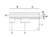
図1は本発明の第1の実施形態に係る半導体記憶装置の断面構成を示している。図1に示すように、例えばシリコンからなるP型ウェル(又はP型半導体基板)1の上部には、素子分離絶縁膜2により区画されたメモリセルアレイ領域Aと保護ダイオード領域Bとが形成されている。
FIG. 1 shows a cross-sectional configuration of a semiconductor memory device according to the first embodiment of the present invention. As shown in FIG. 1, a memory cell array region A and a protection diode region B partitioned by an element
メモリセルアレイ領域Aには、例えば酸化シリコンからなる第1ゲート絶縁膜3、窒化シリコンからなる電荷蓄積層4及び酸化シリコンからなる第2ゲート絶縁膜5が順次形成されてなる、いわゆるONO膜50と、該ONO膜50の上に形成された多結晶シリコン等からなり、ゲート電極を構成する第1導電層12とを有するMONOS(metal oxide-nitride-oxide-semiconductor)型メモリセルが行列状に配置されている。
In the memory cell array region A, for example, a so-called
P型ウェル1の上部における列方向(紙面に垂直な方向)に延びるONO膜50同士の間の領域にはソースドレイン拡散層6が形成され、該ソースドレイン拡散層6と第2導電層13との間には絶縁膜21が形成されている。
A source /
メモリセルアレイ領域Aに隣接する保護ダイオード領域Bには、P型ウェル1の上部に形成されたN型拡散層9が形成されて、該N型拡散層9とP型ウェル1とから保護ダイオード素子が形成されている。
In the protection diode region B adjacent to the memory cell array region A, an N-
メモリセルアレイ領域Aには、メモリセルアレイの行方向に並ぶ複数のメモリセルのゲート電極を共通に接続する例えば多結晶シリコンからなり、ワード線及びゲート電極を構成する第2導電層13が形成されている。第2導電層13は保護ダイオード領域Bにまで延伸して、保護ダイオード領域BにおけるN型拡散層9と直接に接続されている。
In the memory cell array region A, there is formed a second
第1の実施形態によると、第2導電層13が保護ダイオード領域BにおけるP型ウェル1内のN型拡散層9と直接に接続された後は、製造工程で発生する第2導電層13の負の帯電は、PN接合の順方向電圧となる電流パスを持つため、第2導電層13は絶対値が大きい負の電位とならない。また、製造工程で発生するゲート電極の正の帯電に対しても、PN接合の逆方向電圧以上の電位となることはなく、逆方向電圧(耐圧)を10V程度に制御することにより、高電圧の印加によるONO膜50へのストレス又は該ONO膜50の電荷蓄積層4への電荷の注入を防止又は抑制することができる。
According to the first embodiment, after the second
なお、上記の説明は、ゲート電極が第1導電層12と第2導電層13との積層膜により構成され、ワード線が第2導電層13により構成された場合の例である。図2に示すように、ゲート電極及びワード線を第1導電層12のみで形成した場合においても、上記と同様の効果を得ることができる。このことは、第1の実施形態のみならず、以下の各実施形態においても同様にいえる。
The above description is an example in the case where the gate electrode is composed of a laminated film of the first
以下、前記のように構成された第1の実施形態に係る半導体記憶装置の製造方法について図面を参照しながら説明する。 Hereinafter, a method of manufacturing the semiconductor memory device according to the first embodiment configured as described above will be described with reference to the drawings.
まず、図3(a)に示すように、P型ウェル1の上部にシャロウトレンチ分離(Shallow Trench Isolation:STI)構造を持つ素子分離絶縁膜2を選択的に形成する。
First, as shown in FIG. 3A, an element
次に、図3(b)に示すように、例えば化学気相堆積(Chemical Vapor Deposition:CVD)法により、P型ウェル(又はP型半導体基板)1の上に素子分離絶縁膜2を含む全面にわたって、第1ゲート絶縁膜3、電荷蓄積層4、第2ゲート絶縁膜5及び多結晶シリコンからなる第1導電層12を順次形成する。
Next, as shown in FIG. 3B, the entire surface including the element
次に、図3(c)に示すように、リソグラフィ法によるレジストパターン20を用いてドライエッチングにより、メモリセルアレイ領域Aにおける第1導電層12、第2ゲート絶縁膜5、電荷蓄積層4、第1ゲート絶縁膜3を列方向に且つ短冊状にパターニングする。このとき、保護ダイオード領域Bにおいては、P型ウェル1の上面の少なくとも一部が露出する。
Next, as shown in FIG. 3C, the first
次に、図4(a)に示すように、第1導電層12をマスクとして砒素(As)イオン等からなるN型不純物イオンをP型ウェル1に注入することにより、メモリセルアレイ領域Aにはソースドレイン拡散層6を形成し、保護ダイオード領域Bには保護ダイオード素子を構成するN型拡散層9を形成する。
Next, as shown in FIG. 4A, N-type impurity ions made of arsenic (As) ions or the like are implanted into the P-type well 1 using the first
次に、図4(b)に示すように、例えば低圧CVD(low pressure CVD)法により、短冊状にパターニングされた第1導電層12を覆うように、P型ウェル1の上に酸化シリコンからなる絶縁膜21を形成する。
Next, as shown in FIG. 4B, silicon oxide is formed on the P-type well 1 so as to cover the first
次に、図4(c)に示すように、形成された絶縁膜21に対してドライエッチングによるエッチバックを行なって、メモリセルアレイ領域Aにおいては、絶縁膜21から第1導電層12を露出すると共に、保護ダイオード領域Bからは、N型拡散層9を露出する。
Next, as shown in FIG. 4C, the formed insulating
次に、図5に示すように、CVD法により、露出された第1導電層12及びN型拡散層9を含めP型ウェル1の上すなわちウェハ上の全面に多結晶シリコンからなる第2導電層13を形成する。続いて、リソグラフィ法により、第2導電層13の上に行方向(紙面に平行な方向)に延伸する複数の開口パターンを有するレジストパターン(図示せず)を形成し、形成したレジストパターンをマスクとして、行方向に並ぶ複数の第1導電層12同士が電気的に接続されるように、第2導電層13及び第1導電層12をドライエッチングしてワード線を形成する。このとき、ワード線の端部においては、第2導電層13が保護ダイオード領域Bから露出したN型拡散層9に直接に接続された状態が維持されるように、第2導電層13、第1導電層12、ONO膜50及び絶縁膜21をパターニングする。
Next, as shown in FIG. 5, the second conductive layer made of polycrystalline silicon is formed on the P-type well 1 including the exposed first
なお、その後の製造工程については、図示は省略するが、ワード線の上方を含む半導体基板の全体にわたって上層の絶縁膜を形成し、その後、上層の絶縁膜の所定の位置に必要なコンタクトホールを形成する。続いて、コンタクトホールの内部を含む上層の絶縁膜上に配線層を形成する。 Although the illustration of the subsequent manufacturing process is omitted, an upper insulating film is formed over the entire semiconductor substrate including above the word line, and then a necessary contact hole is formed at a predetermined position of the upper insulating film. Form. Subsequently, a wiring layer is formed on the upper insulating film including the inside of the contact hole.
ここで、製造方法の第1変形例として、図3(b)に示したように、保護ダイオード領域Bに、第1ゲート絶縁膜3、電荷蓄積層4及び第2ゲート絶縁膜5からなるONO膜50を形成する代わりに、図6に示すように、少なくともP型ウェル1の全面に、一旦ONO膜50を形成した後、形成したONO膜50における保護ダイオード領域Bに含まれる部分を選択的に除去する。続いて、保護ダイオード領域Bの上に酸化シリコンからなる第3ゲート絶縁膜31を形成し、その後、第1導電層12及び第3ゲート絶縁膜31を形成してもよい。その際、保護ダイオード領域B上における第3ゲート絶縁膜31の除去は、図3(c)に示すドライエッチング又は図4(b)に示す絶縁膜21のドライエッチング時に同時に行なえばよい。このようにすると、図3(c)に示すONO膜50をエッチングする際に、エッチング不足で窒化シリコンからなる電荷蓄積層4が残ってしまい、さらには、その後の図4(b)における絶縁膜21に対するエッチバックを行なう際にも、エッチングレートの違いから窒化シリコンからなる電荷蓄積層4がエッチングされずに残ってしまい、保護ダイオード領域BにおけるN型拡散層9を露出できなくなるという事態を回避することができる。
Here, as a first modification of the manufacturing method, as shown in FIG. 3B, an ONO composed of the first
また、製造方法の第2変形例として、図3(c)において、図7に示すように第1導電層12のみをドライエッチングにより除去し、ONO膜50は残したままでもよい。この場合には、図4(c)において、保護ダイオード領域Bにおける絶縁膜21をドライエッチングによりエッチバックする際に、保護ダイオード領域B上の第1ゲート絶縁膜3、電荷蓄積層4及び第2ゲート絶縁膜5からなるONO膜50を除去することにより、保護ダイオード領域BにおけるN型拡散層9を露出することができる。
As a second modification of the manufacturing method, in FIG. 3C, only the first
以上のような製造方法とすることにより、メモリセルアレイ領域Aにおける第1導電層12の上面を露出すると同時に、拡散ビット線となるソースドレイン拡散層6の上に絶縁膜21を埋め込むことができる。さらに、保護ダイオード領域Bにおいては、第2導電型拡散層9の上の絶縁膜21が除去されて、該第2導電型拡散層9を露出することができる。また、ワード線を構成する第2導電層13を堆積することにより、ワード線と保護ダイオード領域Bの第2導電型拡散層9とが自己整合的に且つ直接に接続されると共に、ワード線は第1導電層12に対しても直接に接続される。
With the manufacturing method as described above, the upper surface of the first
従って、図4(a)〜図4(c)に示すメモリセル形成工程において、保護ダイオード領域Bにおける第2導電型拡散層9の形成及び該第2導電型拡散層9上の絶縁膜21の除去を同時に行なえるため、保護ダイオード素子を形成するための新たな工程が不要となる。
Therefore, in the memory cell formation step shown in FIGS. 4A to 4C, the formation of the second conductivity
以上説明したように、第1の実施形態によると、ワード線を構成する第2導電層13の端部は、保護ダイオード領域Bと直接に接続されているため、ワード線形成用の第2導電層13を堆積した後の製造工程において保護ダイオード素子が機能し、その後のゲート電極及びワード線の帯電による電荷蓄積層4への電荷の注入及びONO膜50へのストレスを防止することができる。
As described above, according to the first embodiment, since the end portion of the second
(第2の実施形態)
以下、本発明の第2の実施形態について図面を参照しながら説明する。
(Second Embodiment)
Hereinafter, a second embodiment of the present invention will be described with reference to the drawings.
図8は本発明の第2の実施形態に係る半導体記憶装置の断面構成を示している。第2の実施形態に係る半導体記憶装置は、第1の実施形態に係る半導体記憶装置におけるデバイス仕様及び保護ダイオード素子の構造を変更している。図8において、図1に示す構成部材と同一の構成部材には同一の符号を付すことにより説明を省略する。 FIG. 8 shows a cross-sectional configuration of a semiconductor memory device according to the second embodiment of the present invention. In the semiconductor memory device according to the second embodiment, the device specification and the structure of the protection diode element in the semiconductor memory device according to the first embodiment are changed. In FIG. 8, the same components as those shown in FIG.
図8に示すように、P型ウェル1は、例えばN型シリコンからなるN型半導体基板14におけるメモリセルアレイ領域A及び保護ダイオード領域Bに分かれて形成されている。
As shown in FIG. 8, the P-
N型半導体基板14の保護ダイオード領域Bには、P型ウェル1のメモリセルアレイ領域Aに対して反対側の領域にN型ウェル15がP型ウェル1と接して形成されている。さらに、保護ダイオード領域BにおけるP型ウェル1とN型ウェル15との接合部の上部には、P型拡散層16が形成されている。
In the protective diode region B of the N-
従って、保護ダイオード領域Bには、N型半導体基板14に形成され、P型ウェル1の上部に形成されたN型拡散層9と、互いに隣接するP型ウェル1及びN型ウェル15と、該P型ウェル1及びN型ウェル15の接合部に跨がるように形成されたP型拡散層16とによって保護ダイオード素子が構成される。
Therefore, in the protection diode region B, the N-
メモリセルアレイ領域Aにおいてワード線を構成する第2導電層13は、保護ダイオード領域Bにまで延伸し、保護ダイオード領域BにおけるP型ウェル1の上部に形成されたN型拡散層9と直接に接続されている。
The second
第2の実施形態によると、ワード線となる第2導電層13が保護ダイオード領域BにおけるP型ウェル1の上部に形成されたN型拡散層9と接続された後は、製造工程で発生するワード線(ゲート電極)に対する負の帯電は、保護ダイオード領域BにおけるP型ウェル1及びN型ウェル15の上部で且つ接合部を跨ぐように形成されたP型拡散層16とN型ウェル15との接合部分においてPN接合の逆方向電圧を生じさせる。従って、逆方向電圧(耐圧)を10V程度に制御することにより、第2導電層13は逆方向電圧よりも絶対値が大きい負の電位とはならない。
According to the second embodiment, after the second
また、製造工程で発生するワード線(ゲート電極)に対する正の帯電においても、保護ダイオード領域BにおけるP型ウェル1と該P型ウェル1の上部に形成されたN型拡散層9との接合部分でPN接合の逆方向電圧を生じさせる。このため、逆方向電圧(耐圧)を10V程度に制御することにより、ワード線は逆方向電圧以上の正の高い電位とはならない。その結果、高電圧の印加によるONO膜50へのストレス又は該ONO膜50の電荷蓄積層4への電荷の注入を抑制することができる。
Further, even in the positive charging with respect to the word line (gate electrode) generated in the manufacturing process, the junction between the P-
さらに、第1の実施形態においては、デバイスの動作時にワード線に負の電圧を印加した場合に、ワード線の負の電位の絶対値を上げることはできないが、第2の実施形態によると、ワード線に負の電圧を印加した場合においても、ワード線の負の電位の絶対値を上げることが可能であるため、ワード線に負電圧を印加可能なデバイスを実現できる。 Furthermore, in the first embodiment, when a negative voltage is applied to the word line during device operation, the absolute value of the negative potential of the word line cannot be increased, but according to the second embodiment, Even when a negative voltage is applied to the word line, the absolute value of the negative potential of the word line can be increased, so that a device that can apply a negative voltage to the word line can be realized.
以上説明したように、第2の実施形態によると、ワード線を構成する第2導電層13の端部は、保護ダイオード領域Bと直接に接続されているため、ワード線形成用の第2導電層13を堆積した後の製造工程において保護ダイオード素子が機能し、その後のゲート電極及びワード線の帯電による電荷蓄積層4への電荷の注入及びONO膜50へのストレスを防止することができる。
As described above, according to the second embodiment, since the end portion of the second
また、ワード線に負電圧を印加する場合においても、保護ダイオード素子が機能するため、ワード線に負電圧を印加するデバイス動作が可能となる。 Further, even when a negative voltage is applied to the word line, the protection diode element functions, so that a device operation that applies a negative voltage to the word line becomes possible.
(第3の実施形態)
以下、本発明の第3の実施形態について図面を参照しながら説明する。
(Third embodiment)
Hereinafter, a third embodiment of the present invention will be described with reference to the drawings.
図9は本発明の第3の実施形態に係る半導体記憶装置の断面構成を示している。第3の実施形態に係る半導体記憶装置は、第2の実施形態に係る半導体記憶装置の第1変形例である。図9において、図8に示す構成部材と同一の構成部材には同一の符号を付すことにより説明を省略する。 FIG. 9 shows a cross-sectional structure of a semiconductor memory device according to the third embodiment of the present invention. The semiconductor memory device according to the third embodiment is a first modification of the semiconductor memory device according to the second embodiment. In FIG. 9, the same components as those shown in FIG.
図9に示すように、保護ダイオード領域Bにおいて互いに隣接するP型ウェル1及びN型ウェル15は、例えばP型シリコンからなるP型半導体基板22に形成された深いN型ウェル17の上部に形成されている。また、保護ダイオード領域Bにおいて、N型ウェル15とP型半導体基板22との上部で且つ接合部を跨ぐようにN型拡散層18が形成されている。
As shown in FIG. 9, the P-
従って、保護ダイオード領域Bには、P型半導体基板22におけるP型ウェル1の上部に形成されたN型拡散層9と、互いに隣接するP型ウェル1及びN型ウェル15と、該P型ウェル1及びN型ウェル15に跨がるように形成されたP型拡散層16と、深いN型ウェル17と、N型ウェル15及びP型半導体基板22の接合部に跨がるように形成されたN型拡散層18とによって保護ダイオード素子が構成される。
Therefore, in the protective diode region B, the N-
第3の実施形態においては、ワード線となる第2導電層13が保護ダイオード領域BにおけるP型ウェル1の上部に形成されたN型拡散層9と接続された後は、製造工程で発生するワード線(ゲート電極)に対する負の帯電は、保護ダイオード領域BにおけるP型ウェル1及びN型ウェル15の上部で且つ接合部を跨ぐように形成されたP型拡散層16とN型ウェル15との接合部分においてPN接合の逆方向電圧を生じさせる。従って、逆方向電圧(耐圧)を10V程度に制御することにより、第2導電層13は逆方向電圧よりも絶対値が大きい負の電位とはならない。
In the third embodiment, after the second
また、製造工程で発生するワード線(ゲート電極)に対する正の帯電は、保護ダイオード領域BにおけるP型ウェル1と該P型ウェル1の上部に形成されたN型拡散層9との接合部分と、保護ダイオード領域BにおけるN型ウェル15とP型半導体基板22との接合部に跨ぐように形成されたN型拡散層18とP型半導体基板22との接合部分の2箇所においてPN接合の逆方向電圧を生じさせる。このため、逆方向電圧(耐圧)を10V程度に制御することにより、ワード線は逆方向電圧以上の正の高い電位とはならない。その結果、高電圧の印加によるONO膜50へのストレス又は該ONO膜50の電荷蓄積層4への電荷の注入を抑制することができる。
Further, the positive charge to the word line (gate electrode) generated in the manufacturing process is caused by the junction between the P-type well 1 in the protective diode region B and the N-
他の変形例として、図10に示すように、保護ダイオード領域Bにおいて、P型ウェル1とN型ウェル15とに跨がるように形成されたP型拡散層16の上部と、N型ウェル15とP型半導体基板22とに跨がるように形成されたN型拡散層18の上部とに、チタン(Ti)、コバルト(Co)又はニッケル(Ni)等の金属とシリコンとの金属化合物からなる第1のシリサイド領域19A及び第2のシリサイド領域19Bをそれぞれ形成してもよい。このようにすると、P型拡散層16及びN型拡散層18を低抵抗化できるため、製造工程においてワード線(ゲート電極)が正又は負に帯電して、ワード線に保護ダイオード素子の逆方向電圧以上の絶対値を持つ電圧が印加された場合に、印加された電圧により発生した電流は、P型半導体基板22に容易に流れるようになる。このため、ONO膜50へのストレス又は該ONO膜50の電荷蓄積層4への電荷の注入をより確実に抑制することが可能となる。
As another modification, as shown in FIG. 10, in the protection diode region B, an upper portion of a P-
(第4の実施形態)
以下、本発明の第4の実施形態について図面を参照しながら説明する。
(Fourth embodiment)
Hereinafter, a fourth embodiment of the present invention will be described with reference to the drawings.
図11は本発明の第4の実施形態に係る半導体記憶装置の断面構成を示している。第4の実施形態に係る半導体記憶装置は、第2の実施形態に係る半導体記憶装置の第2変形例である。図11において、図8に示す構成部材と同一の構成部材には同一の符号を付すことにより説明を省略する。 FIG. 11 shows a cross-sectional structure of a semiconductor memory device according to the fourth embodiment of the present invention. The semiconductor memory device according to the fourth embodiment is a second modification of the semiconductor memory device according to the second embodiment. In FIG. 11, the same components as those shown in FIG.
図11に示すように、保護ダイオード領域Bにおいて互いに隣接するP型ウェル1及びN型ウェル15は、P型シリコンからなるP型半導体基板22に形成された深いN型ウェル17の上部に形成されている。また、保護ダイオード領域Bにおいて、P型拡散層16の上部と、N型ウェル15とP型半導体基板22との接合部分の上部とには、それぞれTiシリサイド等からなる第1のシリサイド領域19A及び第2のシリサイド領域19Bが形成されている。
As shown in FIG. 11, the P-
従って、保護ダイオード領域Bには、P型半導体基板22におけるP型ウェル1の上部に形成されたN型拡散層9と、互いに隣接するP型ウェル1及びN型ウェル15と、該P型ウェル1及びN型ウェル15に跨がるように形成されたP型拡散層16及び第1のシリサイド領域19Aと、深いN型ウェル17と、N型ウェル15及びP型半導体基板22の接合部に跨がるように形成された第2のシリサイド領域19Bとによって保護ダイオード素子が構成される。
Therefore, in the protective diode region B, the N-
第4の実施形態においては、ワード線となる第2導電層13が保護ダイオード領域BにおけるP型ウェル1の上部に形成されたN型拡散層9と接続された後は、製造工程で発生するワード線(ゲート電極)に対する負の帯電は、保護ダイオード領域BにおけるP型ウェル1及びN型ウェル15の上部で且つ接合部を跨ぐように形成されたP型拡散層16とN型ウェル15との接合部分においてPN接合の逆方向電圧を生じさせる。従って、逆方向電圧(耐圧)を10V程度に制御することにより、第2導電層13は逆方向電圧よりも絶対値が大きいの負の電位とはならない。
In the fourth embodiment, after the second
また、製造工程で発生するワード線(ゲート電極)に対する正の帯電は、保護ダイオード領域BにおけるP型ウェル1と該P型ウェル1の上部に形成されたN型拡散層9との接合部分においてPN接合の逆方向電圧を生じさせる。このため、逆方向電圧(耐圧)を10V程度に制御することにより、ワード線は逆方向電圧以上の正の高い電位とはならない。その結果、高電圧の印加によるONO膜50へのストレス又は該ONO膜50の電荷蓄積層4への電荷の注入を抑制することができる。
Further, the positive charging of the word line (gate electrode) generated in the manufacturing process is caused at the junction between the P-
さらに、ワード線に正の高電圧が印加された場合に、第4の実施形態は第3の実施形態と比べて、高電圧による電流がP型半導体基板22に流れるまでに逆方向電圧となる箇所が1箇所のみであるため、耐圧の制御が容易で且つデバイス動作が安定するという効果を有する。
Furthermore, when a positive high voltage is applied to the word line, the fourth embodiment becomes a reverse voltage before the current due to the high voltage flows to the P-
(第5の実施形態)
以下、本発明の第5の実施形態について図面を参照しながら説明する。
(Fifth embodiment)
Hereinafter, a fifth embodiment of the present invention will be described with reference to the drawings.
図12は本発明の第5の実施形態に係る半導体記憶装置の断面構成を示している。第5の実施形態に係る半導体記憶装置は、第3の実施形態に係る半導体記憶装置の第1変形例である。図12において、図9に示す構成部材と同一の構成部材には同一の符号を付すことにより説明を省略する。 FIG. 12 shows a cross-sectional structure of a semiconductor memory device according to the fifth embodiment of the present invention. The semiconductor memory device according to the fifth embodiment is a first modification of the semiconductor memory device according to the third embodiment. In FIG. 12, the same components as those shown in FIG.
図12に示すように、保護ダイオード領域Bにおいて、N型ウェル15におけるP型拡散層16の反対側の上端部にはN型拡散層40が形成され、さらに、P型半導体基板22におけるN型拡散層40に対してP型拡散層16の反対側の上端部には、P型拡散層41が形成されている。ここで、N型拡散層40とP型拡散層41との接合部分は、N型ウェル15とP型半導体基板22との接合部分とほぼ一致している。
As shown in FIG. 12, in the protection diode region B, an N-
従って、保護ダイオード領域Bには、P型半導体基板22におけるP型ウェル1の上部に形成されたN型拡散層9と、互いに隣接するP型ウェル1及びN型ウェル15と、該P型ウェル1及びN型ウェル15に跨がるように形成されたP型拡散層16と、深いN型ウェル17と、N型ウェル15におけるP型拡散層16と反対側の上端部に形成されたN型拡散層40と、P型半導体基板22におけるN型拡散層40に対してP型拡散層16と反対側の上端部に形成されたP型拡散層41とによって保護ダイオード素子が構成される。
Therefore, in the protective diode region B, the N-
第5の実施形態においては、ワード線となる第2導電層13が保護ダイオード領域BにおけるP型ウェル1の上部に形成されたN型拡散層9と接続された後は、製造工程で発生するワード線(ゲート電極)に対する負の帯電は、保護ダイオード領域BにおけるP型ウェル1及びN型ウェル15の上部で且つ接合部を跨ぐように形成されたP型拡散層16とN型ウェル15との接合部分においてPN接合の逆方向電圧を生じさせる。従って、逆方向電圧(耐圧)を10V程度に制御することにより、第2導電層13は逆方向電圧よりも絶対値が大きいの負の電位とはならない。
In the fifth embodiment, after the second
また、製造工程で発生するワード線(ゲート電極)に対する正の帯電は、保護ダイオード領域BにおけるP型ウェル1と該P型ウェル1の上部に形成されたN型拡散層9との接合部分と、保護ダイオード領域BにおけるN型ウェル15の上部に形成されたN型拡散層40とP型半導体基板22の上部に形成されたP型拡散層41との接合部分との2箇所においてPN接合の逆方向電圧を生じさせる。このため、逆方向電圧(耐圧)を10V程度に制御することにより、ワード線は逆方向電圧以上の正の高い電位とはならない。その結果、高電圧の印加によるONO膜50へのストレス又は該ONO膜50の電荷蓄積層4への電荷の注入を抑制することができる。
Further, the positive charge to the word line (gate electrode) generated in the manufacturing process is caused by the junction between the P-type well 1 in the protective diode region B and the N-
ところで、図9に示した第3の実施形態に係る半導体記憶装置の場合、N型拡散層18とP型半導体基板22とのPN接合部は、N型拡散層18を形成した後に高温熱処理が施され、N型拡散層18からN型不純物が拡散する場合に、N型拡散層18とP型半導体基板22とのPN接合付近におけるP型不純物濃度が低くなるため、耐圧を10V程度に低く制御することが困難となるおそれがある。このとき、製造工程においてワード線が正に帯電して、P型ウェル1と該P型ウェル1内のN型拡散層9とのPN接合が10V程度でクランプしたとする。しかしながら、N型拡散層18とP型半導体基板22とのPN接合は耐圧が高いためにクランプせず、P型ウェル1が充電される結果、ワード線の電位は10V以上にまで上昇してしまう場合がある。
Incidentally, in the semiconductor memory device according to the third embodiment shown in FIG. 9, the PN junction between the N-
第5の実施形態においては、P型半導体基板22に形成され、N型拡散層40と接合部を有するP型拡散層41の不純物濃度をP型ウェル1よりも高くすることができるため、上記の問題を回避することができる。
In the fifth embodiment, the impurity concentration of the P-
具体的には、P型拡散層41の不純物濃度をP型ウェル1よりも高くすると、N型拡散層40とP型拡散層41とのPN接合の耐圧を第3の実施形態に係るN型拡散層18とP型半導体基板22とのPN接合の耐圧よりも大幅に低く設定することができる。その結果、上記のような問題を生じることがない、実用的な耐圧を持つ保護ダイオード素子を得ることができる。また、N型拡散層40とP型拡散層41とのPN接合の耐圧を大幅に低く設定することができるため、ワード線が正に帯電した場合の逆方向電圧(耐圧)をP型ウェル1と該P型ウェル1に形成されたN型拡散層9とのPN接合の耐圧のみで制御することが可能となる。
Specifically, when the impurity concentration of the P-
また、一変形例として、図13に示すように、保護ダイオード領域Bにおいて、P型ウェル1とN型ウェル15とに跨がるように形成されたP型拡散層16の上部と、互いに隣接するN型拡散層40及びP型拡散層41の上部とに、第4の実施形態と同様に第1のシリサイド領域19A及び第2のシリサイド領域19Bをそれぞれ形成してもよい。このようにすると、ワード線が正に帯電した場合の逆方向電圧(耐圧)を、P型ウェル1と該P型ウェル1内のN型拡散層9とのPN接合の耐圧のみで制御することが、より容易となり且つデバイス動作が安定する。
As a modification, as shown in FIG. 13, in the protection diode region B, the upper part of the P-
(第6の実施形態)
以下、本発明の第6の実施形態について図面を参照しながら説明する。
(Sixth embodiment)
Hereinafter, a sixth embodiment of the present invention will be described with reference to the drawings.
図14は本発明の第6の実施形態に係る半導体記憶装置の断面構成を示している。図14において、図1に示す構成部材と同一の構成部材には同一の符号を付すことにより説明を省略する。第6の実施形態に係る半導体記憶装置は、第1〜第5の実施形態に係る半導体記憶装置と比べて微細化を可能にする構造を有している。 FIG. 14 shows a cross-sectional structure of a semiconductor memory device according to the sixth embodiment of the present invention. In FIG. 14, the same components as those shown in FIG. The semiconductor memory device according to the sixth embodiment has a structure that enables miniaturization as compared with the semiconductor memory devices according to the first to fifth embodiments.
ところで、図4(c)に示したように、第1の実施形態に係る半導体記憶装置の製造方法においては、P型ウェル1を覆う絶縁膜21をドライエッチングによりエッチバックすることにより、メモリセルアレイ領域Aにおける第1導電膜12を露出すると共に、保護ダイオード領域BにおけるN型拡散層9を露出している。このとき、メモリセルアレイ領域Aにおいては、互いに隣接するメモリセルを構成する第1導電層12同士の間は絶縁膜21で埋め込まれている必要がある。仮に、第1導電層12同士の間の領域に絶縁膜21が埋め込まれていないとすると、第2導電層13がソースドレイン拡散層6と電気的に接続するおそれがあるため、メモリセルを正常に動作させることができない。通常、図4(c)を含む製造方法の場合は、絶縁膜21は低圧CVD法で形成されるが、微細化が進むとメモリセル同士の間隔が小さくなるため、低圧CVD法では第1導電層12の間の領域を完全に埋め込むことができなくおそれがある。
Incidentally, as shown in FIG. 4C, in the method of manufacturing the semiconductor memory device according to the first embodiment, the insulating
また、図4(c)に示す工程において、保護ダイオード領域BにおけるN型拡散層9の表面に絶縁膜21が残った状態となると、第2導電層13がN型拡散層9と接続されない状態となるため、保護ダイオード素子が機能しなくなるおそれがある。微細化が進むと、保護ダイオード領域Bのサイズの縮小が求められる。このため、低圧CVD法で絶縁膜21を堆積した後に、エッチングにより絶縁膜21をエッチバックすると、ONO膜50及び第1導電層12の側面上に形成される絶縁膜21からなるサイドウォールがN型拡散層9を覆ってしまい、前述したような第2導電層13とN型拡散層9が接続できない状態となるおそれがある。
4C, when the insulating
そこで、第6の実施形態においては、本発明の特徴を有し且つ微細化が可能な半導体記憶装置及びその製造方法を説明する。 Therefore, in the sixth embodiment, a semiconductor memory device having the characteristics of the present invention and capable of being miniaturized and a manufacturing method thereof will be described.
図14に示すように、P型ウェル1の上部における列方向に延びるONO膜50同士の間の領域にはソースドレイン拡散層6が形成され、該ソースドレイン拡散層6と第2導電層13との間には、上面が平坦化されたソースドレイン拡散層上絶縁膜33(以下、絶縁膜33と略称する。)が形成されている。第6の実施形態の特徴として、該絶縁膜33は、メモリセルアレイ領域Aにのみに形成され、保護ダイオード領域Bには形成されない。
As shown in FIG. 14, a source /
メモリセルアレイ領域Aに隣接する保護ダイオード領域Bには、第1の実施形態と同様に、P型ウェル1の上部に形成されたN型拡散層9が形成されて、該N型拡散層9とP型ウェル1とから保護ダイオード素子が形成されている。また、N型拡散層9の側端部上には、第1ゲート絶縁膜3、電荷蓄積層4及び第2ゲート絶縁膜からなるONO膜50に代えて、酸化シリコンからなる第3ゲート絶縁膜31が形成されている。
In the protective diode region B adjacent to the memory cell array region A, as in the first embodiment, an N-
メモリセルアレイ領域Aには、メモリセルアレイの行方向に並ぶ複数のメモリセルのゲート電極を共通に接続する例えば多結晶シリコンからなり、ワード線及びゲート電極を構成する第2導電層13が形成されている。第2導電層13は保護ダイオード領域Bにまで延伸して、保護ダイオード領域BにおけるN型拡散層9と直接に接続されている。
In the memory cell array region A, there is formed a second
第6の実施形態によると、第1の実施形態と同様に、製造工程においてONO膜50へのストレス又は該ONO膜50の電荷蓄積層4への電荷の注入を抑制することができる。その上、保護ダイオード領域BにおけるN型拡散層9の上には、サイドウォール状の絶縁膜が形成されないことから、保護ダイオード領域Bのサイズを縮小することができるため、半導体記憶装置の微細化が可能となる。
According to the sixth embodiment, as in the first embodiment, stress on the
以下、前記のように構成された半導体記憶装置の製造方法について図面を参照しながら説明する。 Hereinafter, a method for manufacturing the semiconductor memory device configured as described above will be described with reference to the drawings.
まず、図15(a)に示すように、P型ウェル(又はP型半導体基板)1の上部にSTI構造を持つ素子分離絶縁膜2を選択的に形成する。
First, as shown in FIG. 15A, an element
次に、図15(b)に示すように、例えばCVD法により、P型ウェル1の上に素子分離絶縁膜2を含む全面にわたって、第1ゲート絶縁膜3、電荷蓄積層4及び第2ゲート絶縁膜5を順次形成してONO膜50を形成する。その後、形成されたONO膜50における保護ダイオード領域Bに含まれる部分を選択的に除去する。続いて、保護ダイオード領域Bに露出したP型ウェル1及び素子分離絶縁膜2の上に第3ゲート絶縁膜31を選択的に形成する。続いて、メモリセルアレイ領域A及び保護ダイオード領域Bの上に全面にわたって多結晶シリコンからなる第1導電層12及び窒化シリコンからなるゲート電極加工用絶縁膜32を順次形成する。
Next, as shown in FIG. 15B, the first
次に、図15(c)に示すように、リソグラフィ法及びエッチング法により、メモリセルアレイ領域Aにおいては、ゲート電極加工用絶縁膜32を列方向に且つ短冊状にパターニングすると共に、保護ダイオード領域Bにおいては、ゲート電極加工用絶縁膜32におけるP型ウェル1の上側部分を除去する。その後、パターニングされたゲート電極加工用絶縁膜32をマスクとして、第1導電層12及びその下側の第1ゲート絶縁膜3、電荷蓄積層4、第2ゲート絶縁膜5からなるONO膜50、及び第3ゲート絶縁膜31をドライエッチングによりパターニングする。
Next, as shown in FIG. 15C, in the memory cell array region A, the gate electrode processing insulating
次に、図16(a)に示すように、ゲート電極加工用絶縁膜32をマスクとして砒素(As)等のN型不純物をP型ウェル1に注入して、メモリセルアレイ領域AにはN型のソースドレイン領域6を形成し、保護ダイオード領域Bには保護ダイオード素子を構成するN型拡散層9を形成する。
Next, as shown in FIG. 16A, N-type impurities such as arsenic (As) are implanted into the P-type well 1 using the gate electrode processing insulating
次に、図16(b)に示すように、例えば高密度プラズマCVD(High Density Plasma CVD)法により、酸化シリコンからなる絶縁膜33を、P型ウェル1の全面にゲート電極加工用絶縁膜32を覆うように形成する。
Next, as shown in FIG. 16B, an insulating
次に、図16(c)に示すように、化学機械研磨(Chemical Mechanical Polish:CMP)法により、絶縁膜33をゲート電極加工用絶縁膜32が露出するまで研磨し、その後、ゲート電極加工用絶縁膜32を熱リン酸等を用いたウェットエッチングによって除去する。
Next, as shown in FIG. 16C, the insulating
次に、図16(d)に示すように、リソグラフィ法により、保護ダイオード領域BにおけるN型拡散層9の上側部分に開口部を持つ第1のレジストパターン34を形成する。続いて、形成した第1のレジストパターン34をマスクとして、保護ダイオード領域Bにおける絶縁膜33をドライエッチングすることにより、保護ダイオード領域BからN型拡散層9を露出する。
Next, as shown in FIG. 16D, a first resist
次に、図17(a)に示すように、第1のレジストパターン34を除去した後、CVD法により、露出された第1導電層12及びN型拡散層9を含めP型ウェル1の上すなわちウェハ上の全面に、多結晶シリコンからなる第2導電層13を堆積する。これにより、保護ダイオード領域Bにおいて、第2導電層13がN型拡散層9と直接に接続される。
Next, as shown in FIG. 17A, after removing the first resist
次に、図17(b)に示すように、第2導電層13の上に行方向に延伸する複数の開口パターンを持つ第2のレジストパターン35を形成する。続いて、形成した第2のレジストパターン35をマスクとして、行方向に並ぶ複数の第1導電層12同士が電気的に接続されるように、第2導電層13及び第1導電層12をドライエッチングしてワード線を形成する。このとき、ワード線の端部においては、第2導電層13が保護ダイオード領域Bから露出したN型拡散層9に直接に接続された状態を維持するように、第2導電層13、第1導電層12、ONO膜50及び絶縁膜33をパターニングする。
Next, as shown in FIG. 17B, a second resist
ここで、第1変形例として、図18に示すように、図15(b)に示す工程において保護ダイオード領域Bに第3ゲート絶縁膜を形成する代わりに、保護ダイオード領域BからONO膜50を除去せずに、該ONO膜50を残したまま、第1導電層12及びゲート電極加工用絶縁膜32を形成してもよい。第1変形例の場合には、保護ダイオード領域Bに残るONO膜50は、図15(c)に示す工程におけるドライエッチング、又は図16(d)に示す工程におけるドライエッチングの際に同時に除去することにより、保護ダイオード領域BにおけるN型拡散層9を露出することが可能となる。
Here, as a first modification, as shown in FIG. 18, instead of forming the third gate insulating film in the protection diode region B in the step shown in FIG. 15B, the
また、第2変形例として、図19に示すように、図15(c)に示す工程において第1導電層12のみをドライエッチングにより除去し、メモリセル領域AにおいてはONO膜50を残した状態とし、保護ダイオード領域Bにおいては第3ゲート絶縁膜31を残した状態としてもよい。第2の変形例の場合には、図16(d)において、保護ダイオード領域Bにおける絶縁膜33をドライエッチングにより除去する際に、第3ゲート絶縁膜31をも連続して除去することにより、保護ダイオード領域BにおけるN型拡散層9を露出することが可能となる。
Further, as a second modification, as shown in FIG. 19, only the first
なお、第6の実施形態においては、図16(b)において、高密度プラズマCVD法を用いることにより、低圧CVD法を用いた場合よりも高アスペクト比となる領域への絶縁膜33の埋め込みをより確実に行なえるようにしている。しかしながら、高密度プラズマCVD法により絶縁膜を形成した場合は、成膜直後の絶縁膜の形状が低圧CVD法の場合のように下地膜の形状を反映した形状とはならない。すなわち、ゲート電極加工用絶縁膜32上に形成される絶縁膜33の膜厚は、メモリセル同士の間及び保護ダイオード領域BにおけるP型ウェル1上に形成される絶縁膜33の膜厚よりも小さくなる。
In the sixth embodiment, in FIG. 16B, the high density plasma CVD method is used to embed the insulating
従って、第1の実施形態の図4(c)の工程に示したように、保護ダイオード領域Bに形成された絶縁膜33をエッチングにより除去し、且つメモリセルアレイ領域Aにおける第1導電層12をも露出させようとすると、メモリセル同士の間に形成された絶縁膜33も同時に除去されてしまう。
Therefore, as shown in the step of FIG. 4C of the first embodiment, the insulating
そこで、第6の実施形態においては、図16(c)に示すように、CMP法を用いて第1導電層12上の絶縁膜33を除去している。その後は、図16(d)に示すように、第2のレジストパターン34を用いたエッチングにより、メモリセルアレイ領域Aにおけるメモリセル同士の間の絶縁膜33を残しながら、保護ダイオード領域Bにおける絶縁膜33を確実に除去することができる。
Therefore, in the sixth embodiment, as shown in FIG. 16C, the insulating
以上説明したように、第6の実施形態に係る半導体記憶装置の製造方法によると、図14に示すように、ワード線を構成する第2導電層13は、保護ダイオード素子を構成するP型拡散層9と直接に接続されているため、ワード線形成用の第2の導電層13を堆積した後の工程において保護ダイオード素子が機能する。このため、第2導電層13を堆積した後は、ONO膜50へのストレスを抑制することができる。さらに、メモリセル同士の間の間隔を縮小することができると共に、保護ダイオード領域Bのサイズをも縮小できる。
As described above, according to the method of manufacturing the semiconductor memory device according to the sixth embodiment, as shown in FIG. 14, the second
なお、第6の実施形態においても、保護ダイオード領域Bの構成は、第2〜第5の各実施形態のいずれかと同様の構成を採ってもよい。これは、以下の第7の実施形態及び第8の実施形態においても同様である。 In the sixth embodiment, the configuration of the protection diode region B may be the same as that of any of the second to fifth embodiments. The same applies to the following seventh and eighth embodiments.
(第7の実施形態)
以下、本発明の第7の実施形態について図面を参照しながら説明する。
(Seventh embodiment)
The seventh embodiment of the present invention will be described below with reference to the drawings.
図20は本発明の第7の実施形態に係る浮遊ゲート電極型メモリセルを有する半導体記憶装置の断面構成を示している。図20において、図1に示す構成部材と同一の構成部材には同一の符号を付すことにより説明を省略する。 FIG. 20 shows a cross-sectional structure of a semiconductor memory device having floating gate electrode type memory cells according to the seventh embodiment of the present invention. 20, the description of the same components as shown in FIG. 1 is omitted by retaining the same reference numerals.
前述した第1〜第6の各実施形態においては、メモリセルとして、いずれもゲート絶縁膜50を構成する電荷蓄積層4にシリコン窒化膜を用いたMONOS型を説明した。しかしながら、本発明は、MONOS型メモリセルに限定されず、電荷蓄積層に例えば多結晶シリコンを用いた浮遊ゲート電極型メモリセルに対しても適用可能である。そこで、第7の実施形態においては、浮遊ゲート電極型メモリセルを用いた半導体記憶装置装置とその製造方法について説明する。
In each of the first to sixth embodiments described above, the MONOS type using a silicon nitride film for the
図20に示すように、メモリセルアレイ領域Aにおいて、浮遊ゲート電極型メモリセルは、P型ウェル1と第1導電層12との間にトンネル絶縁膜としてのトンネル酸化膜36が形成され、また、第1導電層12と第2導電層13との間に結合容量絶縁膜37が形成されている。これにより、第1導電層12は結合容量絶縁膜37を介して第2導電層13と容量結合する結果、第1導電層12は浮遊ゲート電極として機能する。
As shown in FIG. 20, in the memory cell array region A, the floating gate electrode type memory cell has a
また、第1〜第6の実施形態と同様に、保護ダイオード領域Bには、P型ウェル1の上部に形成されたN型拡散層9とP型ウェル1とによって保護ダイオード素子が構成されている。ここで、メモリセルアレイ領域Aには、メモリセルアレイの行方向に並ぶ複数のメモリセルのゲート電極を共通に接続する第2導電層13からなるワード線が形成されている。ワード線となる第2導電層13は保護ダイオード領域Bにまで延伸し、保護ダイオード領域BにおけるP型ウェル1の上部に形成されたN型拡散層9と直接に接続されている。
Similarly to the first to sixth embodiments, in the protection diode region B, a protection diode element is configured by the N-
第7の実施形態によると、第1〜第6の実施形態と同様に、製造工程においてゲート絶縁膜(トンネル酸化膜36)へのストレスを抑制することができる。 According to the seventh embodiment, similarly to the first to sixth embodiments, stress on the gate insulating film (tunnel oxide film 36) can be suppressed in the manufacturing process.
以下、前記のように構成された半導体記憶装置の製造方法について図面を参照しながら説明する。 Hereinafter, a method for manufacturing the semiconductor memory device configured as described above will be described with reference to the drawings.
まず、図21(a)に示すように、P型ウェル(又はP型半導体基板)1の上部にSTI構造を持つ素子分離絶縁膜2を選択的に形成する。
First, as shown in FIG. 21A, an element
次に、図21(b)に示すように、例えば熱酸化法又はCVD法により、P型ウェル1の上に素子分離絶縁膜2を含む全面にわたって、酸化シリコンからなるトンネル酸化膜36を形成する。続いて、形成したトンネル酸化膜36の上に、CVD法により多結晶シリコンからなる第1導電層12を形成する。
Next, as shown in FIG. 21B, a
次に、図21(c)に示すように、リソグラフィ法により形成された第1のレジストパターン42を用いて、ドライエッチングにより、メモリセルアレイ領域Aに形成された第1導電層12に対して列方向に且つ短冊状にパターニングすると共に、保護ダイオード領域Bに形成された第1導電層12の少なくとも一部を除去する。
Next, as shown in FIG. 21C, the first resist
次に、図22(a)に示すように、第1のレジストパターン42を除去した後、第1導電層12をマスクとして砒素(As)等のN型不純物をP型ウェル1に注入して、メモリセルアレイ領域AにはN型のソースドレイン領域6を形成し、保護ダイオード領域Bには保護ダイオード素子を構成するN型拡散層9を形成する。
Next, as shown in FIG. 22A, after removing the first resist
次に、図22(b)に示すように、例えば低圧CVD法により、短冊状にパターニングされた第1導電層12を覆うように、トンネル酸化膜36の上に酸化シリコンからなる絶縁膜21を形成する。
Next, as shown in FIG. 22B, an insulating
次に、図22(c)に示すように、形成された絶縁膜21に対してドライエッチングによるエッチバックを行なって、メモリセルアレイ領域Aにおいては絶縁膜21から第1導電層12を露出させると共に、保護ダイオード領域BにおいてはN型拡散層9を露出する。
Next, as shown in FIG. 22C, the formed insulating
次に、図23(a)に示すように、CVD法により、露出された第1導電層12及びN型拡散層9を含めP型ウェル1すなわちウェハの全面にONO膜構造を有する結合容量絶縁膜37を形成する。
Next, as shown in FIG. 23 (a), the coupling capacitance insulation having the ONO film structure on the entire surface of the P-
次に、図23(b)に示すように、リソグラフィ法により、保護ダイオード領域Bの結合容量絶縁膜37を露出する開口パターンを有する第2のレジストパターン43を形成し、形成した第2のレジストパターン43をマスクとして、ドライエッチングにより、保護ダイオード領域Bから結合容量絶縁膜37を除去する。これにより、保護ダイオード領域BのN型拡散層9が露出する。
Next, as shown in FIG. 23B, a second resist
次に、図23(c)に示すように、第2のレジストパターン43を除去した後、CVD法により、結合容量絶縁膜37及び露出されたN型拡散層9を含めP型ウェル1の上すなわちウェハ上の全面に多結晶シリコンからなる第2導電層13を形成する。続いて、リソグラフィ法により、第2導電層13の上に行方向に延伸する複数の開口パターンを有する第3のレジストパターン(図示せず)を形成し、形成した第3のレジストパターンをマスクとして、行方向に並ぶ複数の第1導電層12同士が同一電位となるように、第2導電層13、結合容量絶縁膜37及び第1導電層12をドライエッチングしてワード線を形成する。このとき、ワード線の端部においては、第2導電層13が保護ダイオード領域Bから露出したN型拡散層9に直接に接続された状態を維持するように、第2導電層13、結合容量絶縁膜37、第1導電層12及び絶縁膜21をパターニングする。
Next, as shown in FIG. 23C, after the second resist
以上説明したように、第7の実施形態に係る半導体記憶装置の製造方法によると、図20に示すように、浮遊ゲート電極型メモリセルにおいても、ワード線形成用の第2の導電層13を堆積した後の工程において保護ダイオード素子が機能する。このため、第2の導電層13を堆積した後は、トンネル酸化膜36及び結合容量絶縁膜37へのストレスを抑制することができる。
As described above, according to the manufacturing method of the semiconductor memory device according to the seventh embodiment, as shown in FIG. 20, the second
(第8の実施形態)
以下、本発明の第8の実施形態について図面を参照しながら説明する。
(Eighth embodiment)
Hereinafter, an eighth embodiment of the present invention will be described with reference to the drawings.
図24は本発明の第8の実施形態に係る浮遊ゲート電極型メモリセルを有する半導体記憶装置の断面構成を示している。図24において、図1及び図20に示す構成部材と同一の構成部材には同一の符号を付すことにより説明を省略する。 FIG. 24 shows a cross-sectional structure of a semiconductor memory device having floating gate electrode type memory cells according to the eighth embodiment of the present invention. 24, the same components as those shown in FIGS. 1 and 20 are denoted by the same reference numerals, and the description thereof is omitted.
第8の実施形態は、第7の実施形態と同様に浮遊ゲート電極型メモリセルを有し、さらに第7の実施形態に係る半導体記憶装置よりも微細化が可能な半導体記憶装置とその製造方法について説明する。 The eighth embodiment has a floating gate electrode type memory cell as in the seventh embodiment, and can be further miniaturized than the semiconductor memory device according to the seventh embodiment, and a method for manufacturing the same. Will be described.
第8の実施形態に係る半導体記憶装置は、第7の実施形態と同様に、メモリセルアレイ領域Aにおいて浮遊ゲート電極型メモリセルを有している。浮遊ゲート電極型メモリセルは、P型ウェル1の上に、トンネル酸化膜36、第1導電層12、結合容量絶縁膜37及び第2導電層13からなる積層構造を持つ。第1導電層12は第2導電層13と容量結合絶縁膜37を介して容量結合し、浮遊ゲート電極として機能する。
The semiconductor memory device according to the eighth embodiment has floating gate electrode type memory cells in the memory cell array region A, as in the seventh embodiment. The floating gate electrode type memory cell has a laminated structure including a
また、微細化を可能とするため、第6の実施形態と同様に、ソースドレイン拡散層上絶縁膜(絶縁膜)33は、メモリセルアレイ領域Aにのみに形成されており、保護ダイオード領域Bには形成されていない。 Further, in order to enable miniaturization, the source / drain diffusion layer upper insulating film (insulating film) 33 is formed only in the memory cell array region A and is formed in the protective diode region B as in the sixth embodiment. Is not formed.
保護ダイオード領域Bには、P型ウェル1の上部に形成されたN型拡散層9とP型ウェル1とによって保護ダイオード素子が構成されている。ここで、メモリセルアレイ領域Aには、メモリセルアレイの行方向に並ぶ複数のメモリセルのゲート電極を共通に接続する第2導電層13からなるワード線が形成されている。ワード線となる第2導電層13は保護ダイオード領域Bにまで延伸し、保護ダイオード領域BにおけるP型ウェル1の上部に形成されたN型拡散層9と直接に接続されている。
In the protection diode region B, the N-
第8の実施形態によると、第1〜第7の実施形態と同様に、製造工程においてゲート絶縁膜(トンネル酸化膜36)へのストレスを抑制することができる。また、図24に示す構造により、第6の実施形態と同様に、保護ダイオード領域Bにサイドウォール状の絶縁膜が形成されないことから、保護ダイオード領域Bのサイズを縮小することができるため、半導体記憶装置の微細化が可能となる。 According to the eighth embodiment, similarly to the first to seventh embodiments, stress on the gate insulating film (tunnel oxide film 36) can be suppressed in the manufacturing process. 24, since the sidewall-shaped insulating film is not formed in the protective diode region B, as in the sixth embodiment, the size of the protective diode region B can be reduced. The memory device can be miniaturized.
以下、前記のように構成された半導体記憶装置の製造方法について図面を参照しながら説明する。 Hereinafter, a method for manufacturing the semiconductor memory device configured as described above will be described with reference to the drawings.
まず、図25(a)に示すように、P型ウェル1(又はP型半導体基板)の上部にSTI構造を持つ素子分離絶縁膜2を選択的に形成する。
First, as shown in FIG. 25A, an element
次に、図25(b)に示すように、例えば熱酸化法又はCVD法により、P型ウェル1の上に素子分離絶縁膜2を含む全面にわたって、酸化シリコンからなるトンネル酸化膜36を形成する。続いて、形成したトンネル酸化膜36の上に、CVD法により多結晶シリコンからなる第1導電層12及び窒化シリコンからなるゲート電極加工用絶縁膜32を順次を形成する。
Next, as shown in FIG. 25B, a
次に、図25(c)に示すように、リソグラフィ法及びエッチング法により、メモリセルアレイ領域Aにおいては、ゲート電極加工用絶縁膜32を列方向に且つ短冊状にパターニングすると共に、保護ダイオード領域Bにおいては、ゲート電極加工用絶縁膜32におけるP型ウェル1の上側部分を除去する。その後、パターニングされたゲート電極加工用絶縁膜32をマスクとして、第1導電層12をドライエッチングによりパターニングする。
Next, as shown in FIG. 25C, in the memory cell array region A, the gate electrode processing insulating
次に、図26(a)に示すように、ゲート電極加工用絶縁膜32をマスクとして砒素(As)等のN型不純物をP型ウェル1に注入して、メモリセルアレイ領域AにはN型のソースドレイン領域6を形成し、保護ダイオード領域Bには保護ダイオード素子を構成するN型拡散層9を形成する。
Next, as shown in FIG. 26A, an N-type impurity such as arsenic (As) is implanted into the P-type well 1 using the gate electrode processing insulating
次に、図26(b)に示すように、例えば高密度プラズマCVD法により、酸化シリコンからなるソースドレイン拡散層上絶縁膜(絶縁膜)33を、P型ウェル1の全面にゲート電極加工用絶縁膜32を覆うように形成する。
Next, as shown in FIG. 26B, a source / drain diffusion layer upper insulating film (insulating film) 33 made of silicon oxide is formed on the entire surface of the P-type well 1 by, for example, high-density plasma CVD. The insulating
次に、図26(c)に示すように、化学機械研磨(CMP)法により、絶縁膜33をゲート電極加工用絶縁膜32が露出するまで研磨し、その後、ゲート電極加工用絶縁膜32を熱リン酸等を用いたウェットエッチングによって除去する。
Next, as shown in FIG. 26C, the insulating
次に、図26(d)に示すように、CVD法により、露出された第1導電層12及び絶縁膜33を含めP型ウェル1すなわちウェハの全面にONO膜構造を有する結合容量絶縁膜37を形成する。
Next, as shown in FIG. 26D, a coupling
次に、図27(a)に示すように、リソグラフィ法により、保護ダイオード領域BにおけるN型拡散層9の上側部分に開口部を持つ第1のレジストパターン34を形成する。続いて、形成した第1のレジストパターン34をマスクとして、保護ダイオード領域Bにおける結合容量絶縁膜37、絶縁膜33及びトンネル酸化膜36をドライエッチングすることにより、保護ダイオード領域BからN型拡散層9を露出する。
Next, as shown in FIG. 27A, a first resist
次に、図27(b)に示すように、第1のレジストパターン34を除去した後、CVD法により、露出されたN型拡散層9を含めP型ウェル1の上すなわちウェハ上の全面に、多結晶シリコンからなる第2導電層13を堆積する。これにより、保護ダイオード領域Bにおいて、第2導電層13がN型拡散層9と直接に接続される。
Next, as shown in FIG. 27B, after removing the first resist
次に、図27(c)に示すように、第2導電層13の上に行方向に延伸する複数の開口パターンを持つ第2のレジストパターン35を形成する。続いて、形成した第2のレジストパターン35をマスクとして、行方向に並ぶ複数の第1導電層12同士が同一電位となるように、第2導電層13、結合容量絶縁膜37及び及び第1導電層12をドライエッチングしてワード線を形成する。このとき、ワード線の端部においては、第2導電層13が保護ダイオード領域Bから露出したN型拡散層9に直接に接続された状態を維持するように、第2導電層13、結合容量絶縁膜37、第1導電層12及び絶縁膜33をパターニングする。
Next, as shown in FIG. 27C, a second resist
以上説明したように、第8の実施形態に係る半導体記憶装置の製造方法によると、図24に示すように、浮遊ゲート電極型メモリセルにおいても、ワード線を構成する第2導電層13は、保護ダイオード素子を構成するP型拡散層9と直接に接続されているため、ワード線形成用の第2の導電層13を堆積した後の工程において保護ダイオード素子が機能する。このため、第2導電層13を堆積した後は、トンネル酸化膜36及び結合容量絶縁膜37へのストレスを抑制することができる。さらに、第6の実施形態と同様に、メモリセル同士の間の間隔を縮小することができると共に、保護ダイオード領域Bのサイズをも縮小できる。
As described above, according to the manufacturing method of the semiconductor memory device according to the eighth embodiment, as shown in FIG. 24, in the floating gate electrode type memory cell, the second
(第9の実施形態)
以下、本発明の第9の実施形態について図面を参照しながら説明する。
(Ninth embodiment)
The ninth embodiment of the present invention will be described below with reference to the drawings.
第9の実施形態においては、第3〜第5及び第7の各実施形態で説明した半導体記憶装置に関し、メモリセルに対する書き込み動作、消去動作及び読み出し動作時の駆動方法を説明する。特に、本発明に係る保護ダイオード領域に形成した保護ダイオード素子の場合、複数のPN接合が存在するため、PN接合ごとのノードが不安定な電位とならないように、各ノードの電位を適切に印加する必要がある。 In the ninth embodiment, a driving method during a write operation, an erase operation, and a read operation for a memory cell will be described with respect to the semiconductor memory devices described in the third to fifth and seventh embodiments. In particular, in the case of the protection diode element formed in the protection diode region according to the present invention, since a plurality of PN junctions exist, the potential of each node is appropriately applied so that the node for each PN junction does not become an unstable potential. There is a need to.
図28は第5の実施形態に示した半導体記憶装置において、メモリセルを動作させる場合に必要な端子の構成を示している。VGは、ワード線及びゲート電極を構成する第2導電層13と接続されたゲート端子であり、各メモリセルと接続されたワード線の電位を制御する。VW1は、保護ダイオード領域BにおけるP型ウェル1及びN型ウェル1の上部で且つ接合部に跨がるように形成されたP型拡散層16と接続された第1のウェル端子であり、P型ウェル1の電位を制御する。VW2は、保護ダイオード領域BにおけるP型拡散層40及びN型拡散層41と接続された第2のウェル端子であり、深いN型ウェル17、N型ウェル15及びP型半導体基板22の電位を制御する。
FIG. 28 shows a configuration of terminals necessary for operating a memory cell in the semiconductor memory device shown in the fifth embodiment. VG is a gate terminal connected to the second
図29は第3の実施形態に示した半導体記憶装置において、メモリセルを動作させる場合に必要な端子の構成を示している。VGは、図28と同様に、第2導電層13と接続されたゲート端子であり、各メモリセルのワード線の電位を制御する。VW1は、保護ダイオード領域BのP型拡散層16と接続された第1のウェル端子であり、P型ウェル1の電位を制御する。VW2は、保護ダイオード領域BのN型拡散層18と接続された第2のウェル端子であり、深いN型ウェル17、N型ウェル15及びP型半導体基板22の電位を制御する。
FIG. 29 shows a configuration of terminals necessary for operating a memory cell in the semiconductor memory device shown in the third embodiment. Similarly to FIG. 28, VG is a gate terminal connected to the second
図30は第4の実施形態に示した半導体記憶装置において、メモリセルを動作させる場合に必要な端子の構成を示している。VGは、図28と同様に、第2導電層13と接続されたゲート端子であり、メモリセルのワード線の電位を制御する。VW1は、保護ダイオード領域BのP型拡散層16と第1シリサイド領域19Aを介して接続された第1のウェル端子であり、P型ウェル1の電位を制御する。VW2は、第2シリサイド領域19Bを介して保護ダイオード領域BのN型ウェル15とP型半導体基板22とに接続された第2のウェル端子であり、深いN型ウェル17、N型ウェル15及びP型半導体基板22の電位を制御する。
FIG. 30 shows a configuration of terminals necessary for operating a memory cell in the semiconductor memory device shown in the fourth embodiment. As in FIG. 28, VG is a gate terminal connected to the second
このように、図28、図29及び図30のいずれにおいても、ゲート端子VGはメモリセルのワード線の電位を制御し、第1のウェル端子VW1はP型ウェル1の電位を制御し、第2のウェル端子VW2は深いN型ウェル17、N型ウェル15及びP型半導体基板22の電位を制御する端子である。
As described above, in any of FIGS. 28, 29 and 30, the gate terminal VG controls the potential of the word line of the memory cell, the first well terminal VW1 controls the potential of the P-
図31は本発明に係る半導体記憶装置におけるメモリセルアレイ領域Aと保護ダイオード領域Bとを模式的に示している。ここで、第1のウェル端子VW1及び第2のウェル端子端子VW2は、図28、図29及び図30とそれぞれ対応しており、他の符号も図28、図29又は図30と対応している。また、図28、図29及び図30に示すゲート端子VGは、図31において各ワード線と接続された第1のゲート端子VG1、第2のゲート端子VG2及び第3のゲート端子VG3と対応する。また、ビット線端子VBL1〜VBL4は各ソースドレイン拡散層6と接続された端子である。
FIG. 31 schematically shows a memory cell array region A and a protection diode region B in the semiconductor memory device according to the present invention. Here, the first well terminal VW1 and the second well terminal terminal VW2 correspond to FIG. 28, FIG. 29, and FIG. 30, respectively, and other reference numerals also correspond to FIG. 28, FIG. 29, or FIG. Yes. 28, 29, and 30 correspond to the first gate terminal VG1, the second gate terminal VG2, and the third gate terminal VG3 connected to each word line in FIG. . The bit line terminals VBL 1 to
[表1]に書き込み動作、消去動作及び読み出し動作時における各端子のバイアス条件を示す。いずれも図31に示した選択セルCに対して、書き込み動作及び読み出し動作を行なう。消去動作は選択されたソースドレイン拡散層と接続されたすべてのメモリセルに対して行なわれる。 [Table 1] shows bias conditions of each terminal during a write operation, an erase operation, and a read operation. In either case, a write operation and a read operation are performed on the selected cell C shown in FIG. The erase operation is performed on all the memory cells connected to the selected source / drain diffusion layer.
なお、ここでは、MONOS型メモリセルを想定した動作を示しており、書き込み動作はCHE(Channel Hot Electron)により電子を電荷蓄積層4に注入し、消去動作はBTBT(Band To Band Tunneling)電流によりホールを電荷蓄積層4に注入することにより行なう。
Here, an operation assuming a MONOS type memory cell is shown. In a write operation, electrons are injected into the

(書き込み動作)
まず、書き込み動作について説明する。
(Write operation)
First, the write operation will be described.
書き込み動作は、所定の1ビット、すなわち一のメモリセルに対して行なう必要があるため、選択セルCと接続されたワード線にのみ、正の高電圧を印加する。ここでは、選択ワード線と接続された第2のゲート端子VG2に9Vの電圧を印加する。非選択ワード線と接続された第1のゲート端子VG1及び第2のゲート端子VG3は接地状態(0V)とする。第1のウェル端子VW1及び第2のウェル端子VW2は、接地状態とすることにより、保護ダイオード領域BにおけるP型ウェル1、深いN型ウェル17、N型ウェル15及びP型半導体基板22を0Vの電位とする。このとき、保護ダイオード領域BにおけるN型拡散層9とP型ウェル1とのPN接合には、第2のゲート端子VG2と第1のウェル端子VW1の電位差が逆方向に印加された状態にある。しかしながら、N型拡散層9とP型ウェル1とのPN接合の耐圧が10V程度に設定されていることから、第2のゲート端子VG2と第1のウェル端子VW1との電圧差が9Vであれば、該PN接合がクランプすることなく、常にP型ウェル1は0Vを保った状態となる。
Since the write operation needs to be performed for a predetermined one bit, that is, one memory cell, a positive high voltage is applied only to the word line connected to the selected cell C. Here, a voltage of 9 V is applied to the second gate terminal VG2 connected to the selected word line. The first gate terminal VG1 and the second gate terminal VG3 connected to the unselected word line are set to the ground state (0 V). The first well terminal VW1 and the second well terminal VW2 are grounded, so that the P-
仮に、第1のウェル端子VW1を接地状態とせずに開放状態とした場合は、保護ダイオード領域BのP型ウェル1が不安定な電位となって、選択ワード線の電位の立ち上がりが遅れるおそれがあるため、書き込み速度の低下を招くことにもなる。また、第1のウェル端子VW1を正電位に固定すると、第2のウェル端子VW2と順方向電圧となることから、保護ダイオード領域Bの各ウェル電位が不安定になるため望ましくない。これとは逆に、第1のウェル端子VW1を負電圧に固定すると、ワード線との電位差が大きくなるため、保護ダイオード領域BにおけるN型拡散層9とP型ウェル1とのPN接合との耐圧を高く設定する必要がある。しかしながら、このようにすると、製造中にワード線が受ける帯電による電圧を高くすることになり、電荷蓄積層4への電荷の注入やゲート絶縁膜へのストレスを助長することになる。従って、第1のウェル端子VW1は開放状態とせずに、第2のウェル端子VW2と同一電位の接地状態にする必要がある。
If the first well terminal VW1 is in an open state without being grounded, the P-type well 1 in the protection diode region B becomes an unstable potential, and the rising of the potential of the selected word line may be delayed. For this reason, the writing speed is reduced. In addition, if the first well terminal VW1 is fixed at a positive potential, it becomes a forward voltage with the second well terminal VW2, and therefore, each well potential in the protection diode region B becomes unstable, which is not desirable. On the contrary, if the first well terminal VW1 is fixed to a negative voltage, the potential difference from the word line increases, so that the N-
(消去動作)
次に、消去動作について説明する。
(Erase operation)
Next, the erase operation will be described.
消去動作は、複数ビットを同時に消去する必要がある。本実施形態においては、一のソースドレイン拡散層6と接続されたすべてのメモリセルが消去されるように、全ワード線に絶対値が大きい負の電圧を印加する。ここでは、全ワード線のゲート端子VG1〜VG3に−5Vを印加する。第1のウェル端子VW1には各ゲート端子VG1〜VG3と同一の−5Vを印加する。第2のウェル端子VW2は接地状態として、保護ダイオード領域Bにおける深いN型ウェル17、N型ウェル15及びP型半導体基板22を0Vとする。このとき、保護ダイオード領域BにおけるP型ウェル1とN型ウェル15との電位差は、保護ダイオード領域におけるP型拡散層16とN型ウェル15とのPN接合に対して逆方向電圧となり、且つ耐圧がこの電位差以上に大きく設定されているため、ワード線の負電位がより降下することはない。
The erase operation needs to erase a plurality of bits at the same time. In the present embodiment, a negative voltage having a large absolute value is applied to all word lines so that all memory cells connected to one source /
仮に、第1のウェル端子VW1をワード線と同一の−5Vに設定しない場合は、保護ダイオード領域BのP型ウェル1が不安定な電位となることにより、選択ワード線の電位の立ち上がりが遅れるおそれがあるため、消去速度が低下することにもなる。従って、第1のウェル端子VW1はワード線と同一電位にする必要がある。 If the first well terminal VW1 is not set to the same −5V as that of the word line, the rising of the potential of the selected word line is delayed due to the unstable potential of the P-type well 1 in the protection diode region B. Since there is a fear, the erasing speed may be reduced. Therefore, the first well terminal VW1 needs to have the same potential as the word line.
(読み出し動作)
次に、読み出し動作について説明する。
(Read operation)
Next, the reading operation will be described.
読み出し動作は、所定の1ビット、すなわち一のメモリセルに対して行なう必要があるため、選択セルCと接続されたワード線にのみ正の電圧を印加する。ここでは、選択ワード線と接続された第2のゲート端子VG2に4Vの電圧を印加する。非選択ワード線と接続された第1のゲートの端子VG1及び第3のゲート端子VG3は接地状態(0V)とする。また、第1のウェル端子VW1及び第2のウェル端子VW2は、書き込み動作時と同様に接地状態として、保護ダイオード領域BにおけるP型ウェル1、深いN型ウェル17、N型ウェル15及びP型半導体基板22を0Vとする。このとき、保護ダイオード領域BにおけるN型拡散層9とP型ウェル1とのPN接合には、第2のゲート端子VG2と第1のウェル端子VW1との電位差が逆方向に印加された状態にある。しかしながら、前述した書き込み動作時にPN接合がクランプしないように設定されていれば、読み出し動作はそれ以下の電位差であるため問題は生じない。
Since the read operation needs to be performed on a predetermined one bit, that is, one memory cell, a positive voltage is applied only to the word line connected to the selected cell C. Here, a voltage of 4 V is applied to the second gate terminal VG2 connected to the selected word line. The terminal VG1 and the third gate terminal VG3 of the first gate connected to the unselected word line are set to the ground state (0 V). Further, the first well terminal VW1 and the second well terminal VW2 are grounded as in the write operation, and the P-
仮に、第1のウェル端子VW1を接地状態とせずに開放状態とした場合は、書き込み動作時と同様に、保護ダイオード領域BにおけるP型ウェル1が不安定な電位となることから、選択ワード線の電位の立ち上がりが遅れるおそれがあるため、書き込み速度の低下を招くことにもなる。従って、第1のウェル端子VW1は開放状態とせずに、所定の電位を印加しておく必要がある。 If the first well terminal VW1 is opened without being grounded, the P-type well 1 in the protection diode region B becomes an unstable potential as in the write operation, so that the selected word line There is a possibility that the rise of the potential will be delayed, leading to a decrease in writing speed. Accordingly, it is necessary to apply a predetermined potential to the first well terminal VW1 without opening it.
なお、第9の実施形態においては、MONOS型メモリセルについて説明したが、第7の実施形態又は第8の実施形態に示す浮遊ゲート電極型メモリセルを用いる場合であっても、書き込み動作等の各動作において、ワード線への印加電圧の極性はMONOS型メモリセルと同等であることから、第1のウェル端子VW1及び第2のウェル端子VW2に印加する電位は第9の実施形態と同等とすればよい。このとき、書き込み動作はCHE(Channel Hot Electron)によって電子を電荷蓄積層に注入して行ない、消去動作はF−N(Fowler-Nordheim)電流によって電子を電荷蓄積層から除去することにより行なう。 In the ninth embodiment, the MONOS type memory cell has been described. However, even when the floating gate electrode type memory cell shown in the seventh embodiment or the eighth embodiment is used, a write operation or the like is performed. In each operation, since the polarity of the voltage applied to the word line is equivalent to that of the MONOS type memory cell, the potential applied to the first well terminal VW1 and the second well terminal VW2 is equivalent to that of the ninth embodiment. do it. At this time, the writing operation is performed by injecting electrons into the charge storage layer by CHE (Channel Hot Electron), and the erasing operation is performed by removing the electrons from the charge storage layer by FN (Fowler-Nordheim) current.
以上のように、第9の実施形態に係る半導体記憶装置の駆動方法によると、各ノードの電位を安定に保つことができるため、メモリセルに対する書き込み動作、消去動作及び読み出し動作を安定して行なうことが可能となる。 As described above, according to the driving method of the semiconductor memory device according to the ninth embodiment, the potential of each node can be kept stable, so that the writing operation, the erasing operation, and the reading operation with respect to the memory cell are performed stably. It becomes possible.
なお、上述した第1〜9の各実施形態においてはMONOS型の不揮発性半導体記憶装置又は浮遊ゲート電極型の不揮発性半導体記憶装置を例として挙げたが、これに限定されない。 In each of the first to ninth embodiments described above, the MONOS type nonvolatile semiconductor memory device or the floating gate electrode type nonvolatile semiconductor memory device is given as an example. However, the present invention is not limited to this.
本発明に係る半導体記憶装置及びその製造方法は、高融点金属を含むコンタクトの形成工程から配線層となる導電膜を堆積するまでの間においても、ゲート電極の帯電による高電圧の印加からメモリセルを保護することを可能とし、特に、EEPROM等の不揮発性半導体記憶装置等に有用である。 A semiconductor memory device and a method of manufacturing the same according to the present invention can provide a memory cell from application of a high voltage due to charging of a gate electrode even during a process of forming a contact containing a refractory metal and depositing a conductive film serving as a wiring layer. This is particularly useful for nonvolatile semiconductor memory devices such as EEPROMs.
1 P型ウェル又はP型半導体基板
2 素子分離絶縁膜
3 第1ゲート絶縁膜
4 電荷蓄積層
5 第2ゲート絶縁膜
6 ソースドレイン拡散層
9 N型拡散層
12 第1導電層
13 第2導電層(ワード線)
14 N型半導体基板
15 N型ウェル
16 P型拡散層
17 深いN型ウェル
18 N型拡散層
19A 第1のシリサイド領域
19B 第2のシリサイド領域
20 レジスト
21 絶縁膜
31 第3ゲート絶縁膜
32 ゲート電極加工用絶縁膜
33 ソースドレイン拡散層上絶縁膜(絶縁膜)
34 第1のレジストパターン
35 第2のレジストパターン
36 トンネル酸化膜(トンネル絶縁膜)
37 結合容量絶縁膜
40 N型拡散層
41 P型拡散層
42 第1のレジストパターン
43 第2のレジストパターン
50 ゲート絶縁膜
1 P-type well or P-
14 N-type semiconductor substrate 15 N-type well 16 P-
34 First resist
37 Coupling capacitor insulating film 40 N-type diffusion layer 41 P-
Claims (29)
前記複数のメモリセルのうち、同一の行に並ぶメモリセル同士を共通に接続する複数のワード線と、
第2の半導体領域に前記メモリセルアレイ領域と分離して形成された保護ダイオード領域とを備え、
前記保護ダイオード領域には、前記第2の半導体領域の上部に形成された第1の拡散層と前記第2の半導体領域とが接合してなる保護ダイオード素子が構成され、
前記各ワード線は、前記保護ダイオード領域に延伸して前記第1の拡散層と直接に接続されることにより、前記保護ダイオード素子と電気的に接続されており、
前記第1の半導体領域は、第1導電型であり、
前記第2の半導体領域は、第1導電型ウエルを含み、
前記第1の拡散層は、第2導電型であって、且つ前記第1導電型ウエル内に形成されており、
前記保護ダイオード領域は、前記第1導電型ウエルと、該第1導電型ウエルに隣接して形成された第1の第2導電型ウエルと、前記第1導電型ウエルと前記第1の第2導電型ウエルとの上部で且つ接合部を跨ぐように形成された第1の第1導電型拡散層とを有し、
前記保護ダイオード素子は、前記第1の第2導電型拡散層、第1導電型ウエル、第1の第1導電型拡散層及び第1の第2導電型ウエルにより構成されていることを特徴とする半導体記憶装置。 A memory cell array region formed in a first semiconductor region and having a plurality of memory cells arranged in a matrix;
Among the plurality of memory cells, a plurality of word lines commonly connecting memory cells arranged in the same row;
A protection diode region formed separately from the memory cell array region in a second semiconductor region;
In the protection diode region, a protection diode element formed by joining the first diffusion layer formed on the second semiconductor region and the second semiconductor region is configured,
Each of the word lines is electrically connected to the protection diode element by extending to the protection diode region and directly connected to the first diffusion layer ,
The first semiconductor region is of a first conductivity type;
The second semiconductor region includes a first conductivity type well,
The first diffusion layer is of a second conductivity type and is formed in the first conductivity type well,
The protection diode region includes the first conductivity type well, a first second conductivity type well formed adjacent to the first conductivity type well, the first conductivity type well, and the first second type well. A first conductive type diffusion layer formed on the conductive type well and across the junction;
The protective diode element includes the first second conductivity type diffusion layer, the first conductivity type well, the first first conductivity type diffusion layer, and the first second conductivity type well. A semiconductor memory device.
前記保護ダイオード領域は、前記第1導電型ウエル及び第1の第2導電型ウエルを内包し且つ前記第1導電型ウエル及び第1の第2導電型ウエルよりも接合面が深い第2の第2導電型ウエルと、前記第1の第2導電型ウエルと前記半導体基板との上部で且つ接合部を跨ぐように形成された第2の第2導電型拡散層とを有し、
前記保護ダイオード素子は、前記第1の第2導電型拡散層、第1導電型ウエル、第1の第1導電型拡散層、第1の第2導電型ウエル、第2の第2導電型ウエル及び第2の第2導電型拡散層により構成されていることを特徴とする請求項1に記載の半導体記憶装置。 The first conductivity type well and the first second conductivity type well are formed on a first conductivity type semiconductor substrate,
The protection diode region includes the first conductivity type well and the first second conductivity type well, and has a second junction deeper than the first conductivity type well and the first second conductivity type well. A second conductivity type well, and a second second conductivity type diffusion layer formed above the first second conductivity type well and the semiconductor substrate and across the junction,
The protection diode element includes the first second conductivity type diffusion layer, the first conductivity type well, the first first conductivity type diffusion layer, the first second conductivity type well, and the second second conductivity type well. 2. The semiconductor memory device according to claim 1 , comprising: a second conductive type diffusion layer.
前記保護ダイオード領域は、前記第1導電型ウエル及び第1の第2導電型ウエルを内包し且つ前記第1導電型ウエル及び第1の第2導電型ウエルよりも接合面が深い第2の第2導電型ウエルと、前記第1の第1導電型拡散層の上部に形成された金属による第1のシリサイド領域と、前記第1の第2導電型ウエルと前記半導体基板との上部で且つ接合部を跨ぐように形成された金属による第2のシリサイド領域とを有し、
前記保護ダイオード素子は、前記第1の第2導電型拡散層、第1導電型ウエル、第1の第1導電型拡散層、第1のシリサイド領域、第1の第2導電型ウエル、第2の第2導電型ウエル及び第2のシリサイド領域により構成されていることを特徴とする請求項1に記載の半導体記憶装置。 The first conductivity type well and the first second conductivity type well are formed on a first conductivity type semiconductor substrate,
The protection diode region includes the first conductivity type well and the first second conductivity type well, and has a second junction deeper than the first conductivity type well and the first second conductivity type well. A two-conductivity well, a first silicide region made of metal formed on the first first-conductivity-type diffusion layer, an upper portion of the first second-conductivity well and the semiconductor substrate, and a junction A second silicide region made of metal formed so as to straddle the portion,
The protection diode element includes the first second conductivity type diffusion layer, the first conductivity type well, the first first conductivity type diffusion layer, the first silicide region, the first second conductivity type well, the second 2. The semiconductor memory device according to claim 1 , comprising: a second conductivity type well and a second silicide region.
前記保護ダイオード領域は、前記第1導電型ウエル及び第1の第2導電型ウエルを内包し且つ前記第1導電型ウエル及び第1の第2導電型ウエルよりも接合面が深い第2の第2導電型ウエルと、前記第1の第2導電型ウエルにおける前記第1の第1導電型拡散層と反対側の上部に形成された第2の第2導電型拡散層と、前記半導体基板の上部における前記第2の第2導電型拡散層と隣接して形成された第2の第1導電型拡散層とを有し、
前記保護ダイオード素子は、前記第1の第2導電型拡散層、第1導電型ウエル、第1の第1導電型拡散層、第1の第2導電型ウエル、第2の第2導電型ウエル、第2の第2導電型拡散層及び第2の第1導電型拡散層により構成されていることを特徴とする請求項1に記載の半導体記憶装置。 The first conductivity type well and the first second conductivity type well are formed on a first conductivity type semiconductor substrate,
The protection diode region includes the first conductivity type well and the first second conductivity type well, and has a second junction deeper than the first conductivity type well and the first second conductivity type well. A second conductivity type well, a second second conductivity type diffusion layer formed on an upper side of the first second conductivity type well opposite to the first first conductivity type diffusion layer, and the semiconductor substrate A second first conductivity type diffusion layer formed adjacent to the second second conductivity type diffusion layer in the upper portion;
The protection diode element includes the first second conductivity type diffusion layer, the first conductivity type well, the first first conductivity type diffusion layer, the first second conductivity type well, and the second second conductivity type well. 2. The semiconductor memory device according to claim 1 , comprising: a second second conductivity type diffusion layer and a second first conductivity type diffusion layer.
前記第2の第2導電型拡散層の上部には金属による第2のシリサイド領域が形成されていることを特徴とする請求項2に記載の半導体記憶装置。 A first silicide region made of metal is formed on the first first conductivity type diffusion layer,
3. The semiconductor memory device according to claim 2 , wherein a second silicide region made of metal is formed on the second second conductivity type diffusion layer.
前記第2の第2導電型拡散層の上部及び前記第2の第1導電型拡散層の上部に跨るように、金属による第2のシリサイド領域が形成されていることを特徴とする請求項4に記載の半導体記憶装置。 A first silicide region made of metal is formed on the first first conductivity type diffusion layer,
Claim 4, characterized in that upper and manner across the upper part of the second first-conductivity-type diffusion layer, the second silicide region by the metal of the second second-conductivity-type diffusion layer is formed The semiconductor memory device described in 1.
前記保護ダイオード領域における前記第1の拡散層の上には前記絶縁膜が形成されていないことを特徴とする請求項1に記載の半導体記憶装置。The semiconductor memory device according to claim 1, wherein the insulating film is not formed on the first diffusion layer in the protection diode region.
前記複数のメモリセルのうち、同一の行に並ぶメモリセル同士を共通に接続する複数のワード線と、
第2の半導体領域に前記メモリセルアレイ領域と分離して形成された保護ダイオード領域とを備え、
前記保護ダイオード領域には、前記第2の半導体領域の上部に形成された第1の拡散層と前記第2の半導体領域とが接合してなる保護ダイオード素子が構成され、
前記各ワード線は、前記保護ダイオード領域に延伸して前記第1の拡散層と直接に接続されることにより、前記保護ダイオード素子と電気的に接続されており、
前記第1の半導体領域は、第1導電型であり、
前記第2の半導体領域は、第2導電型ウエルを含み、
前記第1の拡散層は、第1導電型であって、且つ前記第2導電型ウエル内に形成されており、
前記保護ダイオード領域は、前記第2導電型ウエルと、該第2導電型ウエルに隣接して形成された第1の第1導電型ウエルと、前記第2導電型ウエルと前記第1の第1導電型ウエルとの上部で且つ接合部を跨ぐように形成された第1の第2導電型拡散層とを有し、
前記保護ダイオード素子は、前記第1の第1導電型拡散層、第2導電型ウエル、第1の第2導電型拡散層及び第1の第1導電型ウエルにより構成されていることを特徴とする半導体記憶装置。 A memory cell array region formed in a first semiconductor region and having a plurality of memory cells arranged in a matrix;
Among the plurality of memory cells, a plurality of word lines commonly connecting memory cells arranged in the same row;
A protection diode region formed separately from the memory cell array region in a second semiconductor region;
In the protection diode region, a protection diode element formed by joining the first diffusion layer formed on the second semiconductor region and the second semiconductor region is configured,
Each of the word lines is electrically connected to the protection diode element by extending to the protection diode region and directly connected to the first diffusion layer,
The first semiconductor region is of a first conductivity type;
The second semiconductor region includes a second conductivity type well;
The first diffusion layer is of a first conductivity type and is formed in the second conductivity type well,
The protection diode region includes the second conductivity type well, a first first conductivity type well formed adjacent to the second conductivity type well, the second conductivity type well, and the first first type well. A first second conductivity type diffusion layer formed so as to straddle the junction with the conductivity type well;
The protection diode element includes the first first conductivity type diffusion layer, the second conductivity type well, the first second conductivity type diffusion layer, and the first first conductivity type well. semiconductors storage you.
前記保護ダイオード領域は、前記第1の第1導電型ウエルにおける前記第1の第2導電型拡散層と反対側の上部に形成された第2の第1導電型拡散層を有し、
前記保護ダイオード素子は、前記第1の第1導電型拡散層、第2導電型ウエル、第1の第2導電型拡散層、第1の第1導電型ウエル及び第2の第1導電型拡散層により構成されていることを特徴とする請求項8に記載の半導体記憶装置。 The second conductivity type well and the first first conductivity type well are formed on a first conductivity type semiconductor substrate,
The protection diode region has a second first conductivity type diffusion layer formed in an upper portion of the first first conductivity type well opposite to the first second conductivity type diffusion layer;
The protection diode element includes the first first conductivity type diffusion layer, the second conductivity type well, the first second conductivity type diffusion layer, the first first conductivity type well, and the second first conductivity type diffusion. The semiconductor memory device according to claim 8 , comprising a layer.
前記第2の第1導電型拡散層の上部には金属による第2のシリサイド領域が形成されていることを特徴とする請求項9に記載の半導体記憶装置。 A first silicide region made of metal is formed on the first second conductivity type diffusion layer,
10. The semiconductor memory device according to claim 9 , wherein a second silicide region made of a metal is formed on the second first conductivity type diffusion layer.
前記保護ダイオード領域における前記第1の拡散層の上には前記絶縁膜が形成されていないことを特徴とする請求項8に記載の半導体記憶装置。 An insulating film is formed between the memory cells adjacent to each other in the memory cell array region,
9. The semiconductor memory device according to claim 8 , wherein the insulating film is not formed on the first diffusion layer in the protection diode region.
前記半導体領域に素子分離絶縁膜を選択的に形成する工程(a)と、
前記素子分離絶縁膜を含む前記半導体領域の上に、第1のシリコン酸化膜、シリコン窒化膜及び第2のシリコン酸化膜からなるONO膜、並びに第1の導電層を順次形成する工程(b)と、
前記メモリセルアレイ領域において、前記第1の導電層及びONO膜を列方向に延びる短冊状にパターニングすると共に、前記保護ダイオード領域において、前記第1の導電層を除去するようにパターニングする工程(c)と、
前記工程(c)よりも後に、パターニングされた前記第1の導電層をマスクとして、前記半導体領域の前記メモリセルアレイ領域においては、第2導電型拡散層からなり前記メモリセルのソースドレイン領域を形成すると共に、前記半導体領域の前記保護ダイオード領域においては、保護ダイオード素子を構成する第2導電型拡散層を形成する工程(d)と、
前記工程(d)よりも後に、パターニングされた前記第1の導電層を含む前記半導体領域の上に絶縁膜を形成した後、前記メモリセルアレイ領域において、パターニングされた前記第1の導電層の上面を露出する工程(e)と、
前記工程(d)よりも後に、前記保護ダイオード領域において、前記第2導電型拡散層の少なくとも一部を露出する工程(f)と、
前記工程(f)よりも後に、前記半導体領域における前記メモリセルアレイ領域及び保護ダイオード領域の上に第2 の導電層を形成する工程(g)と、
前記工程(g)よりも後に、前記メモリセルアレイ領域において、前記第2の導電層及び第1の導電層を行方向にパターニングすることにより、それぞれ前記第1の導電層を含む行列状に配置された複数の前記メモリセルと、前記第2の導電層からなり同一の行に並ぶ複数の前記メモリセルを共通に接続する複数のワード線とを形成すると共に、前記保護ダイオード領域において、前記保護ダイオード素子の第2導電型拡散層と前記ワード線の端部とを直接に接続する工程(h)とを備えていることを特徴とする半導体記憶装置の製造方法。 A method for manufacturing a semiconductor memory device, wherein a memory cell array region in which a plurality of memory cells are arranged in a matrix and a protection diode region are separately formed on a first conductivity type semiconductor region,
A step (a) of selectively forming an element isolation insulating film in the semiconductor region;
(B) sequentially forming an ONO film made of a first silicon oxide film, a silicon nitride film and a second silicon oxide film, and a first conductive layer on the semiconductor region including the element isolation insulating film; When,
Patterning the first conductive layer and the ONO film in a strip shape extending in the column direction in the memory cell array region, and patterning the first conductive layer in the protection diode region to remove the first conductive layer (c) When,
After the step (c), using the patterned first conductive layer as a mask, in the memory cell array region of the semiconductor region, a source / drain region of the memory cell including a second conductivity type diffusion layer is formed. And, in the protective diode region of the semiconductor region, a step (d) of forming a second conductivity type diffusion layer constituting the protective diode element;
After the step (d), an insulating film is formed on the semiconductor region including the patterned first conductive layer, and then the upper surface of the patterned first conductive layer in the memory cell array region. Exposing step (e);
(F) exposing the at least part of the second conductivity type diffusion layer in the protective diode region after the step (d);
A step (g) of forming a second conductive layer on the memory cell array region and the protection diode region in the semiconductor region after the step (f);
After the step (g), in the memory cell array region, the second conductive layer and the first conductive layer are patterned in a row direction so as to be arranged in a matrix including the first conductive layer, respectively. Forming a plurality of the memory cells and a plurality of word lines that are connected to the plurality of memory cells made of the second conductive layer and arranged in the same row, and in the protection diode region, the protection diode And a step (h) of directly connecting the second conductivity type diffusion layer of the element and the end of the word line.
前記工程(f)は、前記保護ダイオード領域において、前記絶縁膜に対してエッチングを行なうことにより、前記第2導電型拡散層の少なくとも一部を露出する工程であることを特徴とする請求項16に記載の半導体記憶装置の製造方法。 The step (e) is a step of exposing the upper surface of each first conductive layer in the memory cell array region by polishing the formed insulating film by a chemical mechanical polishing method.
Wherein step (f), in the protective diode region, wherein by etching the insulating film, according to claim 16, characterized in that a step of exposing at least a portion of the second conductive type diffusion layer A manufacturing method of the semiconductor memory device according to the above.
前記ONO膜が除去された前記保護ダイオード領域に第3のシリコン酸化膜を選択的に形成する工程とを含むことを特徴とする請求項16〜18のいずれか1項に記載の半導体記憶装置の製造方法。 The step (b) includes a step of selectively removing the ONO film in the protection diode region;
The method according to claim 16 , further comprising: selectively forming a third silicon oxide film in the protection diode region from which the ONO film has been removed. Production method.
前記半導体領域に素子分離絶縁膜を選択的に形成する工程(a)と、
前記素子分離絶縁膜を含む前記半導体領域の上に、トンネル絶縁膜及び第1の導電層を順次形成する工程(b)と、
前記メモリセルアレイ領域において、前記第1の導電層を列方向に延びる短冊状にパターニングすると共に、前記保護ダイオード領域において、前記第1の導電層を除去するようにパターニングする工程(c)と、
前記工程(c)よりも後に、パターニングされた前記第1の導電層をマスクとして、前記半導体領域の前記メモリセルアレイ領域においては、第2導電型拡散層からなり前記メモリセルのソースドレイン領域を形成すると共に、前記半導体領域の前記保護ダイオード領域においては、保護ダイオード素子を構成する第2導電型拡散層を形成する工程(d)と、
前記工程(d)よりも後に、パターニングされた前記第1の導電層を含む前記半導体領域の上に絶縁膜を形成した後、前記メモリセルアレイ領域において、パターニングされた前記第1の導電層の上面を露出する工程(e)と、
前記工程(d)よりも後に、前記保護ダイオード領域において、前記第2導電型拡散層の少なくとも一部を露出する工程(f)と、
前記メモリセルアレイ領域において、上面が露出した前記第1の導電層の上に、結合容量絶縁膜を選択的に形成する工程(g)と、
前記工程(g)よりも後に、前記半導体領域における前記メモリセルアレイ領域及び保護ダイオード領域の上に第2の導電層を形成する工程(h)と、
前記工程(h)よりも後に、前記メモリセルアレイ領域において、前記第2の導電層、結合容量絶縁膜及び第1の導電層を行方向にパターニングすることにより、それぞれ前記第1の導電層及び結合容量絶縁膜を含む行列状に配置された複数の前記メモリセルと、前記第2の導電層からなり同一の行に並ぶ複数の前記メモリセルを共通に接続する複数のワード線とを形成すると共に、前記保護ダイオード領域において、前記保護ダイオード素子の第2導電型拡散層と前記ワード線の端部とを直接に接続する工程(i)とを備えていることを特徴とする半導体記憶装置の製造方法。 A method for manufacturing a semiconductor memory device, wherein a memory cell array region in which a plurality of memory cells are arranged in a matrix and a protection diode region are separately formed on a first conductivity type semiconductor region,
A step (a) of selectively forming an element isolation insulating film in the semiconductor region;
A step (b) of sequentially forming a tunnel insulating film and a first conductive layer on the semiconductor region including the element isolation insulating film;
Patterning the first conductive layer in a strip shape extending in the column direction in the memory cell array region, and patterning the first conductive layer in the protective diode region to remove the first conductive layer;
After the step (c), using the patterned first conductive layer as a mask, in the memory cell array region of the semiconductor region, a source / drain region of the memory cell including a second conductivity type diffusion layer is formed. And, in the protective diode region of the semiconductor region, a step (d) of forming a second conductivity type diffusion layer constituting the protective diode element;
After the step (d), an insulating film is formed on the semiconductor region including the patterned first conductive layer, and then the upper surface of the patterned first conductive layer in the memory cell array region. Exposing step (e);
(F) exposing the at least part of the second conductivity type diffusion layer in the protective diode region after the step (d);
A step (g) of selectively forming a coupling capacitor insulating film on the first conductive layer whose upper surface is exposed in the memory cell array region;
A step (h) of forming a second conductive layer on the memory cell array region and the protection diode region in the semiconductor region after the step (g);
After the step (h), in the memory cell array region, the second conductive layer, the coupling capacitor insulating film, and the first conductive layer are patterned in the row direction, so that the first conductive layer and the coupling are respectively formed. Forming a plurality of memory cells arranged in a matrix including a capacitive insulating film, and a plurality of word lines connected in common to the plurality of memory cells made of the second conductive layer and arranged in the same row. And a step (i) of directly connecting a second conductive type diffusion layer of the protection diode element and an end of the word line in the protection diode region. Method.
前記工程(f)及び(g)は、前記保護ダイオード領域において、前記結合容量絶縁膜及び絶縁膜に対してエッチングを行なうことにより、前記第2導電型拡散層の少なくとも一部を露出する工程であることを特徴とする請求項21に記載の半導体記憶装置の製造方法。 The step (e) is a step of exposing the upper surface of each first conductive layer in the memory cell array region by polishing the formed insulating film by a chemical mechanical polishing method.
The steps (f) and (g) are steps in which at least a part of the second conductivity type diffusion layer is exposed by etching the coupling capacitor insulating film and the insulating film in the protection diode region. The method of manufacturing a semiconductor memory device according to claim 21 , wherein:
前記ワード線に第1の端子を接続し、前記第1の第1導電型拡散層に第2の端子を接続し、前記第2の第2導電型拡散層及び第2の第1導電型拡散層に第3の端子を接続する工程と、
前記第1の端子に正のバイアス電圧を印加する際に、前記第2の端子及び第3 の端子は接地状態とする工程とを備えていることを特徴とする半導体記憶装置の駆動方法。 A method for driving a semiconductor memory device according to claim 4 , wherein:
A first terminal is connected to the word line, a second terminal is connected to the first first conductivity type diffusion layer, and the second second conductivity type diffusion layer and the second first conductivity type diffusion are connected. Connecting a third terminal to the layer;
A method of driving a semiconductor memory device, comprising: applying a positive bias voltage to the first terminal, wherein the second terminal and the third terminal are grounded.
前記ワード線に第1の端子を接続し、前記第1の第1導電型拡散層に第2の端子を接続し、前記第2の第2導電型拡散層及び第2の第1導電型拡散層に第3の端子を接続する工程と、
前記第1の端子に負のバイアス電圧を印加する際に、前記第2の端子には前記第1の端子と同一の電圧を印加し、且つ前記第3の端子は接地状態とする工程とを備えていることを特徴とする半導体記憶装置の駆動方法。 A method for driving a semiconductor memory device according to claim 4 , wherein:
A first terminal is connected to the word line, a second terminal is connected to the first first conductivity type diffusion layer, and the second second conductivity type diffusion layer and the second first conductivity type diffusion are connected. Connecting a third terminal to the layer;
Applying a negative bias voltage to the first terminal, applying the same voltage to the second terminal as the first terminal, and setting the third terminal to a ground state. A method for driving a semiconductor memory device, comprising:
前記ワード線に第1の端子を接続し、前記第1の第1導電型拡散層に第2の端子を接続し、前記第2の第2導電型拡散層に第3の端子を接続する工程と、
前記第1の端子に正のバイアス電圧を印加することにより、選択されたメモリセルに対して書き込み動作又は読み出し動作を行なう工程と、
前記第1の端子に負のバイアス電圧を印加することにより、選択されたメモリセルに対して消去動作を行なう工程とを備えていることを特徴とする半導体記憶装置の駆動方法。 A method for driving a semiconductor memory device according to claim 2 , wherein:
Connecting a first terminal to the word line, connecting a second terminal to the first first conductivity type diffusion layer, and connecting a third terminal to the second second conductivity type diffusion layer; When,
Performing a write operation or a read operation on a selected memory cell by applying a positive bias voltage to the first terminal;
And a step of erasing the selected memory cell by applying a negative bias voltage to the first terminal.
前記ワード線に第1の端子を接続し、前記第1のシリサイド領域に第2の端子を接続し、前記第2のシリサイド領域に第3の端子を接続する工程と、
前記第1の端子に正のバイアス電圧を印加することにより、選択されたメモリセルに対して書き込み動作又は読み出し動作を行なう工程と、
前記第1の端子に負のバイアス電圧を印加することにより、選択されたメモリセルに対して消去動作を行なう工程とを備えていることを特徴とする半導体記憶装置の駆動方法。 A method of driving a semiconductor memory device according to claim 3 ,
Connecting a first terminal to the word line, connecting a second terminal to the first silicide region, and connecting a third terminal to the second silicide region;
Performing a write operation or a read operation on a selected memory cell by applying a positive bias voltage to the first terminal;
And a step of erasing the selected memory cell by applying a negative bias voltage to the first terminal.
Priority Applications (1)
| Application Number | Priority Date | Filing Date | Title |
|---|---|---|---|
| JP2006325510A JP5039368B2 (en) | 2005-12-13 | 2006-12-01 | Semiconductor memory device, manufacturing method thereof and driving method thereof |
Applications Claiming Priority (3)
| Application Number | Priority Date | Filing Date | Title |
|---|---|---|---|
| JP2005358969 | 2005-12-13 | ||
| JP2005358969 | 2005-12-13 | ||
| JP2006325510A JP5039368B2 (en) | 2005-12-13 | 2006-12-01 | Semiconductor memory device, manufacturing method thereof and driving method thereof |
Publications (3)
| Publication Number | Publication Date |
|---|---|
| JP2007189204A JP2007189204A (en) | 2007-07-26 |
| JP2007189204A5 JP2007189204A5 (en) | 2009-04-09 |
| JP5039368B2 true JP5039368B2 (en) | 2012-10-03 |
Family
ID=38344120
Family Applications (1)
| Application Number | Title | Priority Date | Filing Date |
|---|---|---|---|
| JP2006325510A Expired - Fee Related JP5039368B2 (en) | 2005-12-13 | 2006-12-01 | Semiconductor memory device, manufacturing method thereof and driving method thereof |
Country Status (1)
| Country | Link |
|---|---|
| JP (1) | JP5039368B2 (en) |
Cited By (3)
| Publication number | Priority date | Publication date | Assignee | Title |
|---|---|---|---|---|
| US9802374B2 (en) | 2006-11-03 | 2017-10-31 | Tufts University | Biopolymer sensor and method of manufacturing the same |
| US9969134B2 (en) | 2006-11-03 | 2018-05-15 | Trustees Of Tufts College | Nanopatterned biopolymer optical device and method of manufacturing the same |
| US10040834B2 (en) | 2006-11-03 | 2018-08-07 | Tufts University | Biopolymer optofluidic device and method of manufacturing the same |
Families Citing this family (4)
| Publication number | Priority date | Publication date | Assignee | Title |
|---|---|---|---|---|
| JP5274878B2 (en) * | 2008-04-15 | 2013-08-28 | パナソニック株式会社 | Semiconductor device and manufacturing method thereof |
| JP5259246B2 (en) * | 2008-05-09 | 2013-08-07 | ルネサスエレクトロニクス株式会社 | Semiconductor device |
| JP6292041B2 (en) * | 2014-06-11 | 2018-03-14 | 富士通セミコンダクター株式会社 | Semiconductor device and manufacturing method thereof |
| JPWO2023281795A1 (en) * | 2021-07-09 | 2023-01-12 |
Family Cites Families (6)
| Publication number | Priority date | Publication date | Assignee | Title |
|---|---|---|---|---|
| JPH10173157A (en) * | 1996-12-06 | 1998-06-26 | Toshiba Corp | Semiconductor device |
| JPH10200077A (en) * | 1997-01-08 | 1998-07-31 | Sony Corp | Semiconductor device and its manufacturing method |
| JP3528575B2 (en) * | 1998-02-17 | 2004-05-17 | セイコーエプソン株式会社 | Nonvolatile semiconductor memory device and method of manufacturing the same |
| JP2002164447A (en) * | 2000-11-28 | 2002-06-07 | Sharp Corp | Manufacturing method of non-volatile semiconductor memory |
| US6940152B2 (en) * | 2002-02-21 | 2005-09-06 | Matsushita Electric Industrial Co., Ltd. | Semiconductor storage device and its manufacturing method |
| JP4163610B2 (en) * | 2003-12-22 | 2008-10-08 | 株式会社東芝 | Nonvolatile semiconductor memory device |
-
2006
- 2006-12-01 JP JP2006325510A patent/JP5039368B2/en not_active Expired - Fee Related
Cited By (4)
| Publication number | Priority date | Publication date | Assignee | Title |
|---|---|---|---|---|
| US9802374B2 (en) | 2006-11-03 | 2017-10-31 | Tufts University | Biopolymer sensor and method of manufacturing the same |
| US9969134B2 (en) | 2006-11-03 | 2018-05-15 | Trustees Of Tufts College | Nanopatterned biopolymer optical device and method of manufacturing the same |
| US10040834B2 (en) | 2006-11-03 | 2018-08-07 | Tufts University | Biopolymer optofluidic device and method of manufacturing the same |
| US10280204B2 (en) | 2006-11-03 | 2019-05-07 | Tufts University | Electroactive biopolymer optical and electro-optical devices and method of manufacturing the same |
Also Published As
| Publication number | Publication date |
|---|---|
| JP2007189204A (en) | 2007-07-26 |
Similar Documents
| Publication | Publication Date | Title |
|---|---|---|
| JP5191633B2 (en) | Semiconductor device and manufacturing method thereof | |
| JP4758625B2 (en) | Semiconductor device | |
| JP6591291B2 (en) | Semiconductor device and manufacturing method thereof | |
| JP4818061B2 (en) | Nonvolatile semiconductor memory | |
| TWI408800B (en) | Nonvolatile memory cell and method for fabricating the same | |
| JP5086558B2 (en) | Semiconductor device and manufacturing method thereof | |
| JP5039368B2 (en) | Semiconductor memory device, manufacturing method thereof and driving method thereof | |
| JP2008530771A (en) | Electrically rewritable non-volatile memory cell for storing multiple data and manufacturing method thereof | |
| JP2006005357A (en) | Split-gate type flash memory element and method of manufacturing the same | |
| US8409949B2 (en) | Non-volatile semiconductor memory device and method of manufacturing the same | |
| US7474548B2 (en) | Semiconductor memory device and method for manufacturing the same | |
| KR100953050B1 (en) | Nonvolatile memory device and method of manufacturing the same | |
| CN106024889B (en) | Semiconductor device and method for manufacturing the same | |
| US6432773B1 (en) | Memory cell having an ONO film with an ONO sidewall and method of fabricating same | |
| CN100568508C (en) | Symmetrical and self aligned non-volatile memory architecture | |
| JP6786440B2 (en) | Semiconductor devices and their manufacturing methods | |
| CN101000924A (en) | Semiconductor memory device and method for producing the same | |
| JP2019117913A (en) | Semiconductor device and manufacturing method thereof | |
| US7611946B2 (en) | Method of fabricating a non-volatile memory device | |
| JP4758951B2 (en) | Semiconductor device | |
| KR20000076852A (en) | Semiconductor memory device and method of manufacturing the same | |
| US11205655B2 (en) | Method for manufacturing semiconductor device including fin-structured transistor | |
| JP2009194221A (en) | Semiconductor device and its production process | |
| JP2006310564A (en) | Nonvolatile semiconductor memory and its manufacturing method | |
| US20120037974A1 (en) | Semiconductor device and method of manufacturing the same |
Legal Events
| Date | Code | Title | Description |
|---|---|---|---|
| A521 | Request for written amendment filed |
Free format text: JAPANESE INTERMEDIATE CODE: A523 Effective date: 20090224 |
|
| A621 | Written request for application examination |
Free format text: JAPANESE INTERMEDIATE CODE: A621 Effective date: 20090224 |
|
| A977 | Report on retrieval |
Free format text: JAPANESE INTERMEDIATE CODE: A971007 Effective date: 20110519 |
|
| RD02 | Notification of acceptance of power of attorney |
Free format text: JAPANESE INTERMEDIATE CODE: A7422 Effective date: 20120120 |
|
| A131 | Notification of reasons for refusal |
Free format text: JAPANESE INTERMEDIATE CODE: A131 Effective date: 20120417 |
|
| A521 | Request for written amendment filed |
Free format text: JAPANESE INTERMEDIATE CODE: A523 Effective date: 20120522 |
|
| TRDD | Decision of grant or rejection written | ||
| A01 | Written decision to grant a patent or to grant a registration (utility model) |
Free format text: JAPANESE INTERMEDIATE CODE: A01 Effective date: 20120612 |
|
| A01 | Written decision to grant a patent or to grant a registration (utility model) |
Free format text: JAPANESE INTERMEDIATE CODE: A01 |
|
| A61 | First payment of annual fees (during grant procedure) |
Free format text: JAPANESE INTERMEDIATE CODE: A61 Effective date: 20120709 |
|
| FPAY | Renewal fee payment (event date is renewal date of database) |
Free format text: PAYMENT UNTIL: 20150713 Year of fee payment: 3 |
|
| R150 | Certificate of patent or registration of utility model |
Ref document number: 5039368 Country of ref document: JP Free format text: JAPANESE INTERMEDIATE CODE: R150 Free format text: JAPANESE INTERMEDIATE CODE: R150 |
|
| R250 | Receipt of annual fees |
Free format text: JAPANESE INTERMEDIATE CODE: R250 |
|
| R250 | Receipt of annual fees |
Free format text: JAPANESE INTERMEDIATE CODE: R250 |
|
| R250 | Receipt of annual fees |
Free format text: JAPANESE INTERMEDIATE CODE: R250 |
|
| R250 | Receipt of annual fees |
Free format text: JAPANESE INTERMEDIATE CODE: R250 |
|
| R250 | Receipt of annual fees |
Free format text: JAPANESE INTERMEDIATE CODE: R250 |
|
| R250 | Receipt of annual fees |
Free format text: JAPANESE INTERMEDIATE CODE: R250 |
|
| R250 | Receipt of annual fees |
Free format text: JAPANESE INTERMEDIATE CODE: R250 |
|
| R250 | Receipt of annual fees |
Free format text: JAPANESE INTERMEDIATE CODE: R250 |
|
| S533 | Written request for registration of change of name |
Free format text: JAPANESE INTERMEDIATE CODE: R313533 |
|
| R350 | Written notification of registration of transfer |
Free format text: JAPANESE INTERMEDIATE CODE: R350 |
|
| S111 | Request for change of ownership or part of ownership |
Free format text: JAPANESE INTERMEDIATE CODE: R313113 |
|
| R350 | Written notification of registration of transfer |
Free format text: JAPANESE INTERMEDIATE CODE: R350 |
|
| LAPS | Cancellation because of no payment of annual fees |