JP5025552B2 - Touch panel - Google Patents
Touch panel Download PDFInfo
- Publication number
- JP5025552B2 JP5025552B2 JP2008106811A JP2008106811A JP5025552B2 JP 5025552 B2 JP5025552 B2 JP 5025552B2 JP 2008106811 A JP2008106811 A JP 2008106811A JP 2008106811 A JP2008106811 A JP 2008106811A JP 5025552 B2 JP5025552 B2 JP 5025552B2
- Authority
- JP
- Japan
- Prior art keywords
- light
- receiving element
- light receiving
- light source
- light guide
- Prior art date
- Legal status (The legal status is an assumption and is not a legal conclusion. Google has not performed a legal analysis and makes no representation as to the accuracy of the status listed.)
- Expired - Fee Related
Links
Images


Landscapes
- Position Input By Displaying (AREA)
Description
本発明は、タッチパネルに関するものであり、特に、光学式タッチパネルの改良に関するものである。 The present invention relates to a touch panel, and particularly relates to an improvement of an optical touch panel.
従来、ディスプレイ装置の表示面に装着されるタッチパネルとして、光学式、抵抗膜式、静電容量式、超音波式等の各種方式が知られている。 Conventionally, various types such as an optical type, a resistive film type, a capacitance type, and an ultrasonic type are known as a touch panel mounted on a display surface of a display device.
そのうち、光学式タッチパネルとしては、例えば、特許文献1に液晶ディスプレイパネル等の表示装置上に配置する導光板の側面に光源と検知用ラインセンサが配置されたタッチパネルが開示されている。このタッチパネルは、光を導光体の側面の光源から供給し、入力ペン等の光吸収により変化する光信号を光源に対向して配置された検知用ラインセンサで検知する。 Among them, as an optical touch panel, for example, Patent Document 1 discloses a touch panel in which a light source and a detection line sensor are disposed on a side surface of a light guide plate disposed on a display device such as a liquid crystal display panel. This touch panel supplies light from a light source on the side surface of the light guide, and detects an optical signal that changes due to light absorption by an input pen or the like with a detection line sensor disposed opposite the light source.
また、特許文献2には液晶ディスプレイの画面の前面に平面状の検出範囲を備え、鏡を検出範囲の一方の側部にのみ設け、鏡を設けた辺と直交する一方の辺側に光リニアセンサと赤外線発光体を設けた位置検出装置が開示されている。直接指示棒に向けて放射された赤外光は、指示棒の先端の再帰反射球の再帰反射機能により入射方向に反射され、実像としてセンサに入力される。 Further, Patent Document 2 includes a flat detection range on the front surface of a liquid crystal display screen, a mirror is provided only on one side of the detection range, and an optical linear is provided on one side orthogonal to the side where the mirror is provided. A position detection device provided with a sensor and an infrared light emitter is disclosed. The infrared light directly emitted toward the indicator bar is reflected in the incident direction by the retroreflection function of the retroreflective sphere at the tip of the indicator bar, and is input to the sensor as a real image.
赤外線発光体の赤外光の一部は、鏡で反射して指示棒の先端の再帰反射球に入射する。再帰反射球の再帰反射機能により赤外光は入射方向に反射され、鏡で再度反射され赤外線発光体の方向に戻っていく。この反射光は写像としてセンサに入力される。そして、実像の位置情報及び写像の位置情報より指示棒の位置を求める。
特許文献1のタッチパネルでは、入力ペン等の光吸収による光信号の変化を検知する方式であるため、外来光の入射によりコントラストが低下する。また、特許文献2の位置検出装置は、鏡に直接外来光が入射する構成であるため、鏡に対して垂直に近い角度で入射する外来光は光リニアセンサに入射し、入射した外来光の情報を含めて一計算がなされる。従って、特許文献1や特許文献2ものでは、タッチ位置の認識精度が外来光によって低下するという問題点があった。 Since the touch panel of Patent Document 1 is a method of detecting a change in an optical signal due to light absorption by an input pen or the like, the contrast is reduced by the incidence of external light. In addition, since the position detection device of Patent Document 2 has a configuration in which extraneous light is directly incident on the mirror, the extraneous light incident at an angle near to the mirror is incident on the optical linear sensor, and the incident extraneous light is incident on the mirror. A calculation is made including the information. Therefore, in Patent Document 1 and Patent Document 2, there is a problem that the recognition accuracy of the touch position is lowered by external light.
本発明の目的は、外来光の影響を低減し、タッチ位置の認識精度を向上させることが可能なタッチパネルを提供することにある。 An object of the present invention is to provide a touch panel that can reduce the influence of extraneous light and improve the accuracy of touch position recognition.
本発明のタッチパネルは、接触した被検出体の位置を検知するための第1の面と、前記第1の面に対向する第2の面とを有する導光手段と、
前記導光手段に光を入射する光源と、
前記導光手段の側面の一部に配置された受光素子と、
前記導光手段の側面と前記受光素子との間に配置され、前記第1の面に接触した前記被検出体により散乱した前記光源からの光を前記受光素子に結像する結像手段と、を有するタッチパネルにおいて、
前記受光素子が配置された前記導光手段の側面の一部を除く側面の少なくとも一部に光を吸収する光吸収手段が配置され、前記受光素子は前記光源の照射範囲外に配置されており、
前記結像手段はスリットもしくはピンホールであり、
前記スリットもしくはピンホールと前記受光素子との間に前記導光手段と屈折率が等しく、前記光源の波長に対して透明な樹脂が充填されていることを特徴とする。
The touch panel according to the present invention includes a light guide having a first surface for detecting the position of the object to be detected, and a second surface facing the first surface,
A light source for entering light into the light guide means;
A light receiving element disposed on a part of a side surface of the light guiding means;
An imaging unit that is disposed between a side surface of the light guide unit and the light receiving element and forms an image on the light receiving element of light from the light source scattered by the detected object in contact with the first surface; In a touch panel having
The light receiving element is disposed a light absorbing means for absorbing light in at least a portion of the side surface excluding the portion of the side surface of the light guide means is disposed, the light receiving element are arranged outside the irradiation range of the light source ,
The imaging means is a slit or a pinhole,
The light guide means has a refractive index equal to that between the slit or pinhole and the light receiving element, and is filled with a resin transparent to the wavelength of the light source .
本発明のタッチパネルは、接触した被検出体の位置を検知するための第1の面と、前記第1の面に対向する第2の面とを有する導光手段と、
前記導光板の端面の一部に配置された複数の光源と、
前記導光板の端面の一部に配置された複数の受光素子と、
前記導光板の端面と前記受光素子の各々の間に配置され、前記被検出体により散乱された前記光源からの光をそれぞれ前記複数の受光素子に結像する結像手段と、を有するタッチパネルにおいて、
前記導光手段の端面のうち前記受光素子が配置された前記導光手段の端面以外の端面の少なくとも一部に光を吸収する光吸収手段が配置され、
前記複数の光源は各々前記複数の受光素子のいずれかと対を成しており、前記複数の受光素子の光検出期間は各々対を成す前記光源の点灯期間に内包され、且つ、対を成さない前記光源の点灯期間とは重複しておらず、
前記結像手段はスリットもしくはピンホールであり、
前記スリットもしくはピンホールと前記受光素子との間に前記導光手段と屈折率が等しく、前記光源の波長に対して透明な樹脂が充填されていることを特徴とする。
The touch panel according to the present invention includes a light guide having a first surface for detecting the position of the object to be detected, and a second surface facing the first surface,
A plurality of light sources arranged on a part of an end surface of the light guide plate;
A plurality of light receiving elements arranged on a part of the end face of the light guide plate;
In a touch panel, comprising: an imaging unit that is disposed between an end face of the light guide plate and each of the light receiving elements, and forms an image on each of the plurality of light receiving elements of light from the light source scattered by the detected body ,
A light absorbing means for absorbing light is disposed on at least a part of an end face of the light guide means other than the end face of the light guide means on which the light receiving element is disposed;
Each of the plurality of light sources is paired with one of the plurality of light receiving elements, and a light detection period of each of the plurality of light receiving elements is included in a lighting period of the pair of light sources, and forms a pair. There is no overlap with the lighting period of the light source ,
The imaging means is a slit or a pinhole,
The light guide means has a refractive index equal to that between the slit or pinhole and the light receiving element, and is filled with a resin transparent to the wavelength of the light source .
本発明のタッチパネルによれば、外来光の影響を低減でき、タッチ位置の認識精度を向上させることができる。 According to the touch panel of the present invention, the influence of external light can be reduced, and the recognition accuracy of the touch position can be improved.
次に、発明を実施するための最良の形態について図面を参照して詳細に説明する。なお、本発明は以下の実施形態の内容に限定されるものではない。 Next, the best mode for carrying out the invention will be described in detail with reference to the drawings. In addition, this invention is not limited to the content of the following embodiment.
(第1の実施形態)
図1(A)は本発明に係るタッチパネルの第1の実施形態を示す図である。図1(A)は斜視図、図1(B)は図1(A)の受光素子104の周辺の拡大図である。検知用導光板である導光板101は接触した対象物の位置を検知するため、接触面の第1の面と、第1の面に対向する第2の面とを有する。導光板101の材料には、ガラスもしくはアクリルやプラスチック等様々な材質が用いられる。
(First embodiment)
FIG. 1A is a diagram showing a first embodiment of a touch panel according to the present invention. 1A is a perspective view, and FIG. 1B is an enlarged view of the periphery of the light receiving element 104 in FIG. 1A. The light guide plate 101 serving as a detection light guide plate has a first surface of the contact surface and a second surface opposite to the first surface in order to detect the position of the contacted object. As the material of the light guide plate 101, various materials such as glass, acrylic and plastic are used.
この材料には、導光板101の第1面(表面)、第2面(裏面)に配置される物質に比べてある程度大きな屈折率を有する物体で、且つ、透明度がある程度高い物体であればどのような材料でも良い。本実施形態では、導光板101の表面側、裏面側の物質を空気とする。測定の対象物である被検出体201には、例えば、指や入力ペン等が一般的に用いられる。光源102は被検出体201を導光板101を介して照射する光源であり、波長λ0の光を発光する。タッチパネルはディスプレイ上に配置するため、光源102の波長は非可視光であることが好ましく、シリコン系の受光素子の感度特性等から赤外線であることが好ましい。 This material can be any material that has a refractive index that is somewhat larger than the substances placed on the first surface (front surface) and the second surface (back surface) of the light guide plate 101 and that has a certain degree of transparency. Such materials may be used. In the present embodiment, the material on the front side and the back side of the light guide plate 101 is air. For example, a finger, an input pen, or the like is generally used for the detected object 201 that is an object to be measured. The light source 102 is a light source that irradiates the detection target 201 through the light guide plate 101, and emits light having a wavelength λ 0 . Since the touch panel is disposed on the display, the wavelength of the light source 102 is preferably non-visible light, and infrared light is preferable from the sensitivity characteristics of the silicon-based light receiving element.
更に、太陽光のスペクトルには、950nm付近に大気中の水蒸気の吸収による極小値が存在することが知られており、屋外の強烈な太陽光下での使用を考慮すると、波長λ0は950±20nmであることが好ましい。光源102からの出射光は照射範囲103に照射される。受光素子104と導光板101の間及び受光素子105と導光板101の間には、それぞれ光源102の発光波長λ0を主に選択的に透過し、それ以外の光は透過しない波長選択フィルタ106が配置されている。受光素子104、105はライン方向に複数の画素が配列されたラインセンサである。 Furthermore, it is known that there is a local minimum in the spectrum of sunlight due to absorption of water vapor in the atmosphere in the vicinity of 950 nm. Considering the use under intense sunlight outdoors, the wavelength λ 0 is 950. It is preferably ± 20 nm. Light emitted from the light source 102 is irradiated to the irradiation range 103. Between the light receiving element 104 and the light guide plate 101 and between the light receiving element 105 and the light guide plate 101, the wavelength selective filter 106 that mainly selectively transmits the emission wavelength λ 0 of the light source 102 and does not transmit other light. Is arranged. The light receiving elements 104 and 105 are line sensors in which a plurality of pixels are arranged in the line direction.
波長選択フィルタ106は光源102の波長λ0よりも短波長側の光をカットするが、長波長側の光もカットするバンドパスフィルタであればより望ましい。導光板101と波長選択フィルタ106の間に結像手段107が配置されている。結像手段107はレンズであるが、スリットやピンホール等が好適に用いられる。導光板101の側面には光吸収手段108が配置されている。光吸収手段108は光源102が配置された側面を除く少なくとも一部の側面に配置されている。光吸収手段108には、例えば、カーボンブラック含有樹脂が用いられる。 The wavelength selection filter 106 cuts light on the shorter wavelength side than the wavelength λ 0 of the light source 102, but is more preferably a bandpass filter that also cuts light on the longer wavelength side. An imaging means 107 is disposed between the light guide plate 101 and the wavelength selection filter 106. The imaging means 107 is a lens, but a slit, a pinhole or the like is preferably used. Light absorbing means 108 is disposed on the side surface of the light guide plate 101. The light absorbing means 108 is disposed on at least a part of the side surfaces excluding the side surface on which the light source 102 is disposed. For the light absorption means 108, for example, a carbon black-containing resin is used.
次に、本実施形態の動作を説明する。導光板101の側面に配置された光源102から照射された光は導光板101の内部で全反射を繰り返しながら伝播する。光源102による照射範囲103の導光板101表面に接触した被検出体201は導光板101の表面に存在するエバネッセント光等を散乱する。散乱された光の一部は導光板101内部で全反射を繰り返しながら受光素子104、105が配置された導光板101の側面にまで伝播する。この光は結像手段107により受光素子104、105上に結像される。 Next, the operation of this embodiment will be described. Light emitted from the light source 102 disposed on the side surface of the light guide plate 101 propagates while repeating total reflection inside the light guide plate 101. The detected object 201 that is in contact with the surface of the light guide plate 101 in the irradiation range 103 by the light source 102 scatters evanescent light or the like existing on the surface of the light guide plate 101. Part of the scattered light propagates to the side surface of the light guide plate 101 on which the light receiving elements 104 and 105 are arranged while repeating total reflection inside the light guide plate 101. This light is imaged on the light receiving elements 104 and 105 by the imaging means 107.
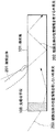
受光素子104、105で検知される信号強度の測定例を図2(B)に示す。横軸は受光素子上の画素番号であり、縦軸は受光素子で検知された光信号強度である。各受光素子はライン方向に複数の画素が配列されており、画素番号とは受光素子のライン方向の画素の位置を表す。ここで、信号強度は本来画素軸に対して離散的な値をとりうるが、ここでは模式的に連続的な曲線でデータを例示する。 A measurement example of the signal intensity detected by the light receiving elements 104 and 105 is shown in FIG. The horizontal axis is the pixel number on the light receiving element, and the vertical axis is the optical signal intensity detected by the light receiving element. Each light receiving element has a plurality of pixels arranged in the line direction, and the pixel number represents the position of the pixel in the line direction of the light receiving element. Here, the signal intensity can originally take a discrete value with respect to the pixel axis, but here, the data is schematically illustrated by a continuous curve.
なお、図2(B)の横軸の画素番号と図1(A)の受光素子104、105との対応は次の通りである。即ち、図2(B)の横軸の左側は、導光板の第1面を上にして受光素子の導光板とは反対側から受光素子を見て受光素子104の左側の画素、受光素子105の左側の画素に対応する。さらに、図2(B)の横軸の左側は、導光板の第1面を上にして各受光素子から導光板を見て右側のタッチ位置に対応する。 The correspondence between the pixel numbers on the horizontal axis in FIG. 2B and the light receiving elements 104 and 105 in FIG. 1A is as follows. That is, the left side of the horizontal axis in FIG. 2B is a pixel on the left side of the light receiving element 104 when the light receiving element is viewed from the side opposite to the light guide plate of the light receiving element with the first surface of the light guide plate facing up, the light receiving element 105. Corresponds to the pixel on the left side of. Furthermore, the left side of the horizontal axis in FIG. 2B corresponds to the right touch position when the light guide plate is viewed from each light receiving element with the first surface of the light guide plate facing up.
図2(A)に示すように被検出体210、受光素子104、受光素子105を結ぶ三角形のうち、受光素子104、105間の距離111はタッチパネル固有の値である。受光素子104の光信号112の位置(画素番号)から角度αが、受光素子105の光信号113の位置(画素番号)から角度βが計測できる。三角測量の原理から被検出体201の座標を計算する。 As shown in FIG. 2A, among the triangles connecting the detected object 210, the light receiving element 104, and the light receiving element 105, the distance 111 between the light receiving elements 104 and 105 is a value unique to the touch panel. The angle α can be measured from the position (pixel number) of the optical signal 112 of the light receiving element 104, and the angle β can be measured from the position (pixel number) of the optical signal 113 of the light receiving element 105. The coordinates of the detected object 201 are calculated from the principle of triangulation.
次に、本実施形態の効果を説明する。まず、図1(A)に示すようにタッチパネルを構成するいずれの部品も導光板101の端面に配置されているため、薄型化が可能となる。例えば、第2面側に検知用の光源やセンサを設けると装置が厚くなってしまう。そのため、本発明の構成は薄型化に好適である。 Next, the effect of this embodiment will be described. First, as shown in FIG. 1A, since any component constituting the touch panel is disposed on the end face of the light guide plate 101, the thickness can be reduced. For example, if a light source or sensor for detection is provided on the second surface side, the apparatus becomes thick. Therefore, the configuration of the present invention is suitable for thinning.
また、受光素子104、105を光源102の照射範囲103の外に配置することで、光源102からの直接光が入射するのを防止できる。更に、光源102、受光素子104、105が配置されている部分を除き、光を吸収する光吸収手段108を配置している。そのため、被検出体201により散乱された光が導光板101の端面で反射され、受光素子104、105に到達することでゴースト信号となるのを防止することができる。 In addition, by arranging the light receiving elements 104 and 105 outside the irradiation range 103 of the light source 102, direct light from the light source 102 can be prevented from entering. Further, a light absorbing means 108 that absorbs light is disposed except for a portion where the light source 102 and the light receiving elements 104 and 105 are disposed. Therefore, it is possible to prevent the light scattered by the detection target 201 from being reflected by the end face of the light guide plate 101 and reaching the light receiving elements 104 and 105 to become a ghost signal.
また、図3に示すように被検出体201を介して導光板101内部に侵入した外来光202は被検出体201が散乱した光源102からの光と同様に被検出体201の位置情報を有するため座標検出に利用できる。一方、導光板101表面に接触した被検出体201の位置情報を持たない外来光203は導光板101の端面に配置された光吸収手段108により吸収され、導光板101内部に侵入しない。このような構成とすることで、薄型化をしつつ外来光に対する影響を軽減することが可能となる。 Further, as shown in FIG. 3, the extraneous light 202 that has entered the light guide plate 101 through the detected object 201 has positional information of the detected object 201 in the same manner as the light from the light source 102 scattered by the detected object 201. Therefore, it can be used for coordinate detection. On the other hand, extraneous light 203 that does not have position information of the detected object 201 in contact with the surface of the light guide plate 101 is absorbed by the light absorbing means 108 disposed on the end face of the light guide plate 101 and does not enter the light guide plate 101. With such a configuration, it is possible to reduce the influence on external light while reducing the thickness.
(第2の実施形態)
図4は本発明の第2の実施形態を示す図である。図4(A)は平面図、図4(B)は図4(A)の受光素子104周辺の拡大図である。図4では図1と同一の部分には同一符号を付している。第1の実施形態との違いはミラー114を導光板101の端面に設けている点である。また、受光素子105及びそれに付随する波長選択フィルタや結像手段は配置されていない。
(Second Embodiment)
FIG. 4 is a diagram showing a second embodiment of the present invention. 4A is a plan view, and FIG. 4B is an enlarged view around the light receiving element 104 in FIG. 4A. In FIG. 4, the same parts as those in FIG. The difference from the first embodiment is that the
ミラー114が配置された導光板101の端面は、受光素子104が配置された端面及び受光素子104が配置された端面と隣り合う端面以外の端面である。本実施形態の動作のうち、被検出体201から直接受光素子104に至る実像からの光204の拳動は第1の実施形態と同様である。
The end surface of the light guide plate 101 on which the
図4(A)に示すように被検出体201が散乱した光のうちミラー114に反射して受光素子104に入射する光は、被検出体201の虚像201aからの光205として受光素子104にて観測される。このような構成とすることで、図5に示す様に被検出体201が散乱した光の実像からの光信号115と虚像201aからの光信号116の二つの信号を一つの受光素子104で観測することが可能となる。その結果、被検出体201の座標を一つの受光素子104で計算することが可能となる。図5の横軸と受光素子との対応は図2(B)の場合と同様である。
As shown in FIG. 4A, light that is reflected by the
本実施形態によれば、第1の実施形態の効果に加えて、受光素子及びそれに付随する波長選択フィルタ、或いは結像手段等の数を減らすことが可能となるため、コスト削減が可能となる。 According to the present embodiment, in addition to the effects of the first embodiment, it is possible to reduce the number of light receiving elements and wavelength selection filters associated therewith, or image forming means, thereby enabling cost reduction. .
(第3の実施形態)
図6は本発明の第3の実施形態を示す図である。本実施形態では、光源102aと光源102bが導光板101の対向する側面に配置されている。また、受光素子104aと104bが配置されている。光源102aと受光素子104aは対を成しており、光源102bと受光素子104bは対を成すものである。
(Third embodiment)
FIG. 6 is a diagram showing a third embodiment of the present invention. In the present embodiment, the light source 102 a and the light source 102 b are disposed on the opposite side surfaces of the light guide plate 101. In addition, light receiving elements 104a and 104b are arranged. The light source 102a and the light receiving element 104a make a pair, and the light source 102b and the light receiving element 104b make a pair.
光源102aと102bは図1の光源102と同じものであり、受光素子104a及び受光素子104bは図1の受光素子104と同じものである。その他の構成は図1と同様である。図6では図1と同一の部分には同一符号を付している。 The light sources 102a and 102b are the same as the light source 102 in FIG. 1, and the light receiving element 104a and the light receiving element 104b are the same as the light receiving element 104 in FIG. Other configurations are the same as those in FIG. In FIG. 6, the same parts as those in FIG.
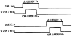
図6(A)は平面図であり、光源102aが点灯している状態を示す。図6(B)は同様に平面図であり、光源102bが点灯している状態を示す。受光素子の周辺の拡大図は省略しているが、図1(B)或いは図4(B)等と同様である。図7は図6の各光源の点灯期間、各受光素子の光検出期間の関係を示す。横軸は経過時間、縦軸は点灯及び光検出の有無を示す。 FIG. 6A is a plan view showing a state where the light source 102a is turned on. FIG. 6B is similarly a plan view showing a state where the light source 102b is lit. Although an enlarged view of the periphery of the light receiving element is omitted, it is the same as FIG. 1B or 4B. FIG. 7 shows the relationship between the lighting period of each light source in FIG. 6 and the light detection period of each light receiving element. The horizontal axis represents elapsed time, and the vertical axis represents the presence or absence of lighting and light detection.
第1及び第2の実施形態との違いは、対を成す複数の光源102aと受光素子104a及び光源102bと受光素子104bを導光板101の端面に設けている点である。受光素子104aは対を成す光源102aの照射範囲103a外に配置され、受光素子104bは対を成す光源102bの照射範囲103b外に配置されている。 The difference from the first and second embodiments is that a plurality of light sources 102 a and light receiving elements 104 a and light sources 102 b and light receiving elements 104 b forming a pair are provided on the end surface of the light guide plate 101. The light receiving element 104a is arranged outside the irradiation range 103a of the paired light sources 102a, and the light receiving element 104b is arranged outside the irradiation range 103b of the paired light sources 102b.
図7に示すように受光素子104aの光検出期間118aは、対を成す光源102aの点灯期間117aに内包され、受光素子104bの光検出期間118bは対を成す光源102bの点灯期間117bに内包される。光源102aの点灯期間117aは光源102bの点灯期間117bとは重複しない。すなわち、光源102aの点灯期間117aは受光素子104bの光検出期間118bとは重複しない。 As shown in FIG. 7, the light detection period 118a of the light receiving element 104a is included in the lighting period 117a of the paired light sources 102a, and the light detection period 118b of the light receiving element 104b is included in the lighting period 117b of the paired light sources 102b. The The lighting period 117a of the light source 102a does not overlap with the lighting period 117b of the light source 102b. That is, the lighting period 117a of the light source 102a does not overlap with the light detection period 118b of the light receiving element 104b.
本実施形態の動作のうち、光源102a或いは102bから照射された光を被検出体201が散乱し、散乱光の一部が導光板101を伝播して受光素子104a或いは104bで検知する一連の動作は第1の実施形態と同じである。 Among the operations of the present embodiment, a series of operations in which light to be detected from the light source 102a or 102b is scattered by the detected object 201 and a part of the scattered light propagates through the light guide plate 101 and is detected by the light receiving element 104a or 104b. Is the same as in the first embodiment.
ここで、光源102aの点灯期間117a中、被検出体201で光源102aからの光が散乱されたとする。散乱された光の一部は導光板内部で全反射を繰り返しながら受光素子104aが配置された導光板101の端面にまで伝播する。この光は不図示の結像手段により受光素子104a上に結像される。 Here, it is assumed that light from the light source 102a is scattered by the detected object 201 during the lighting period 117a of the light source 102a. A part of the scattered light propagates to the end face of the light guide plate 101 where the light receiving element 104a is arranged while repeating total reflection inside the light guide plate. This light is imaged on the light receiving element 104a by imaging means (not shown).
この時、図7に示すように受光素子104bは点灯期間117aには受光しないので、図6(A)に示すように位置的には光源102aの照射範囲内であっても光源102aからの直接光を検出することは無い。また、同様の理由で図6(B)に示すように受光素子104aは位置的には光源102bの照射範囲内であっても光源102bからの直接光を検出することは無い。 At this time, as shown in FIG. 7, the light receiving element 104b does not receive light during the lighting period 117a. Therefore, as shown in FIG. 6A, even if the position is within the irradiation range of the light source 102a, the light receiving element 104b directly receives light from the light source 102a. There is no detection of light. For the same reason, as shown in FIG. 6B, the light receiving element 104a does not detect the direct light from the light source 102b even if it is within the irradiation range of the light source 102b.
複数の光源及び受光素子を配置する場合、第1の実施形態では全ての光源の照射範囲外に全ての受光素子を配置しなければならない。本実施形態では、対を成す光源の照射範囲外に受光素子を配置するだけで済み、第1の実施形態と比較して光源及び受光素子の配置に自由度が増すという効果が得られる。 When arranging a plurality of light sources and light receiving elements, in the first embodiment, all the light receiving elements must be arranged outside the irradiation range of all the light sources. In the present embodiment, it is only necessary to arrange the light receiving elements outside the irradiation range of the paired light sources, and an effect of increasing the degree of freedom in the arrangement of the light sources and the light receiving elements can be obtained as compared with the first embodiment.
(第4の実施形態)
図8は本発明の第4の実施形態を示す図である。本実施形態では結像手段としてスリットを使ったタッチパネルを示す。図8では図1と同一部分には同一符号を付している。図8(A)は図1の受光素子104近辺の構成を示す。受光素子105の近辺も同様である。その他の構成は図1と同様である。
(Fourth embodiment)
FIG. 8 is a diagram showing a fourth embodiment of the present invention. In the present embodiment, a touch panel using a slit as an imaging means is shown. In FIG. 8, the same parts as those in FIG. FIG. 8A shows a configuration in the vicinity of the light receiving element 104 in FIG. The same applies to the vicinity of the light receiving element 105. Other configurations are the same as those in FIG.
具体的には、図8(A)に示すようにスリット121と受光素子104の間に屈折率が導光板101と略等しく光源102からの光に対して透明な樹脂119を充填している。図8(A)にはその場合の信号光の軌跡を示す。図8(B)は図8(A)の構成に対して樹脂119を充填していない点が異なる。図8(B)には信号光の軌跡を示す。 Specifically, as shown in FIG. 8A, a resin 119 having a refractive index substantially equal to that of the light guide plate 101 and transparent to the light from the light source 102 is filled between the slit 121 and the light receiving element 104. FIG. 8A shows a locus of signal light in that case. FIG. 8B is different from the structure of FIG. 8A in that the resin 119 is not filled. FIG. 8B shows a locus of signal light.
本実施形態では図8(A)、図8(B)の両構成が可能である。波長選択フィルタ106は省略しているが、透明な樹脂119にその機能を持たせても良い。120aは導光板101の屈折率と空気の屈折率から決まる導光板101から空気中に抜ける臨界角未満の角度でスリット121に到達した信号光の軌跡を示す。120bは臨界角以上の角度でスリット121に到達した信号光の軌跡を示す。本実施形態のその他の動作は第1の実施形態の説明と同様である。 In this embodiment, both configurations shown in FIGS. 8A and 8B are possible. Although the wavelength selection filter 106 is omitted, the transparent resin 119 may have the function. Reference numeral 120a denotes a trajectory of the signal light that has reached the slit 121 at an angle less than a critical angle that passes through the light guide plate 101 into the air determined from the refractive index of the light guide plate 101 and the refractive index of air. Reference numeral 120b denotes a trajectory of the signal light that has reached the slit 121 at an angle greater than the critical angle. Other operations in the present embodiment are the same as those described in the first embodiment.
本実施形態では、結像手段107としてスリット121を使用することによりレンズを使用する場合に比べてコストが抑えられる。図8(A)に示すように樹脂119を充填した場合には、導光板101と空気層の界面が無いため、臨界角による制限が無くなり、より広い角度の信号光が受光素子104に到達し、受光素子から見た視野角が広がるという効果が得られる。更に、透明樹脂119に信号光の波長は透過するが、それ以外の波長の光を遮断するフィルタ機能を付加することにより、部品点数を削減できるという効果が得られる。 In the present embodiment, the use of the slit 121 as the imaging means 107 can reduce the cost compared to the case where a lens is used. When the resin 119 is filled as shown in FIG. 8A, there is no interface between the light guide plate 101 and the air layer, so there is no restriction by the critical angle, and signal light with a wider angle reaches the light receiving element 104. The effect of widening the viewing angle viewed from the light receiving element can be obtained. Furthermore, although the wavelength of the signal light is transmitted to the transparent resin 119, an effect that the number of parts can be reduced can be obtained by adding a filter function for blocking light of other wavelengths.
図8(A)、図8(B)の構成は図1、図4、図6の実施形態の結像手段としてのレンズの代わりに使用することが可能である。また、後述する図9に示す実施形態にも使用可能である。 The configurations shown in FIGS. 8A and 8B can be used in place of the lens as the imaging means in the embodiments shown in FIGS. It can also be used in an embodiment shown in FIG.
(第5の実施形態)
図9は本発明の第5の実施形態を示す図である。図9(A)は斜視図、図9(B)は受光素子周辺の拡大図を示す。図9では図1、図4等と同一部分には同一符号を付している。本実施形態では、図1や図4等の構成に液晶ディスプレイ115、バックライト用導光板116等が追加され、検知用の光源102が表示用光源105と同様にバックライト用導光板116に配置されている。
(Fifth embodiment)
FIG. 9 is a diagram showing a fifth embodiment of the present invention. FIG. 9A is a perspective view, and FIG. 9B is an enlarged view around the light receiving element. In FIG. 9, the same parts as those in FIGS. In the present embodiment, a liquid crystal display 115, a backlight light guide plate 116, and the like are added to the configuration of FIGS. 1 and 4, and the detection light source 102 is arranged on the backlight light guide plate 116 in the same manner as the display light source 105. Has been.
検知用の導光板101の材料には、ガラスもしくはアクリルやプラスチック等様々な材質が用いられる。この材料には、導光板101の第1面(表面)、第2面(裏面)に配置される物質に比べてある程度大きな屈折率を有する物体で、且つ、透明度がある程度高い物体であればどのような材料でも良い。本実施形態では、導光板101の表面側、裏面側の物質を同様に空気とする。 As a material of the light guide plate 101 for detection, various materials such as glass, acrylic or plastic are used. This material can be any material that has a refractive index that is somewhat larger than the substances placed on the first surface (front surface) and the second surface (back surface) of the light guide plate 101 and that has a certain degree of transparency. Such materials may be used. In the present embodiment, the material on the front side and the back side of the light guide plate 101 is similarly air.
本実施形態では、導光板101の下部に液晶ディスプレイ115が配置され、液晶ディスプレイ115の下には表示用のバックライト用導光板116が配置されている。図9ではバックライトを構成する光学フィルム類は省略している。 In the present embodiment, a liquid crystal display 115 is disposed below the light guide plate 101, and a backlight light guide plate 116 for display is disposed below the liquid crystal display 115. In FIG. 9, the optical films constituting the backlight are omitted.
バックライト用導光板116の端面には表示用光源105及び検知用の光源102が配置されている。表示用光源105は一般に白色光源である。光源102は被検出体201に照射する光源であり、波長λ0の光を発光する。液晶ディスプレイ115は表示の有無に関らず波長λ0の光の大部分を透過する。 A display light source 105 and a detection light source 102 are disposed on the end face of the backlight light guide plate 116. The display light source 105 is generally a white light source. The light source 102 is a light source that irradiates the detection target 201 and emits light having a wavelength λ 0 . The liquid crystal display 115 transmits most of the light having the wavelength λ 0 regardless of whether the display is present.
タッチパネルは液晶ディスプレイ115上に配置されるため、光源102の波長は非可視光であることが好ましく、シリコン系の受光素子の感度特性等から赤外線であることが好ましい。更に、太陽光のスペクトルには、950nm付近に大気中の水蒸気による吸収による極小値が存在するので、屋外の強烈な太陽光下での使用を考慮すると波長λ0は950±20nmであることが好ましい。 Since the touch panel is disposed on the liquid crystal display 115, the wavelength of the light source 102 is preferably non-visible light, and is preferably infrared from the sensitivity characteristics of the silicon-based light receiving element. Furthermore, in the spectrum of sunlight, there is a minimum value due to absorption by water vapor in the atmosphere in the vicinity of 950 nm. Therefore, when considering use under intense sunlight outdoors, the wavelength λ 0 may be 950 ± 20 nm. preferable.
103は光源102の照射範囲を示す。受光素子104の前には光源102の発光波長λ0を主に選択的に透過し、それ以外の光は透過しない波長選択フィルタ106が配置されている。波長選択フィルタ106は光源102の波長λ0よりも短波長側の光をカットするが、長波長側の光もカットするバンドパスフィルタであれば尚良い。 Reference numeral 103 denotes an irradiation range of the light source 102. In front of the light receiving element 104, a wavelength selection filter 106 that mainly selectively transmits the light emission wavelength λ 0 of the light source 102 and does not transmit other light is disposed. The wavelength selection filter 106 cuts light on the shorter wavelength side than the wavelength λ 0 of the light source 102, but may be a band-pass filter that also cuts light on the longer wavelength side.
107は結像手段、108は光吸収手段である。114は図4と同様のミラーである。光源102の照射光は光源102の照射範囲103に接触した被検出体201により散乱され、その光がミラー114で反射されて受光素子104に入射する。その場合、光源102の照射光が直接ミラー114に反射して受光素子104には入射しないように導光板101の端面に受光素子104が配置されている。
Reference numeral 107 denotes an image forming means, and 108 denotes a light absorbing means.
本実施形態では、光源102はバックライト用導光板116の端面に配置された表示用光源105に併設されている。光源102から照射された光は全反射を繰り返しながらバックライト用導光板116の内部を伝播し、表示用光源105と同様に液晶ディスプレイ115の表示面に対して垂直な方向に光を発する面光源となる。光源102の照射範囲103に接触した被検出体201により光源102からの照明光が散乱され、散乱された光の一部は導光板101内部で全反射を繰り返しながら受光素子104が配置された導光板101の端面にまで伝播する。 In the present embodiment, the light source 102 is provided side by side with the display light source 105 disposed on the end face of the backlight light guide plate 116. The light emitted from the light source 102 propagates through the backlight light guide plate 116 while repeating total reflection, and emits light in a direction perpendicular to the display surface of the liquid crystal display 115 like the display light source 105. It becomes. Illumination light from the light source 102 is scattered by the detected object 201 that is in contact with the irradiation range 103 of the light source 102, and a part of the scattered light is totally guided inside the light guide plate 101 while the light receiving element 104 is disposed. It propagates to the end face of the optical plate 101.
この光は結像手段107により受光素子104上に結像される。散乱された光の一部は導光板101内部で全反射を繰り返しながらミラー114に到達する。ミラー114により反射された散乱光は導光板101内部で全反射を繰り返しながら受光素子104が配置された導光板101の端面にまで伝播する。この光は結像手段107により受光素子104上に結像される。
This light is imaged on the light receiving element 104 by the imaging means 107. A part of the scattered light reaches the
受光素子104で検知される信号強度の測定例を図10(B)に示す。横軸は受光素子上の画素番号であり、縦軸が受光素子で検知された光信号強度である。受光素子は上述のように長手方向に複数の画素が配列されており、画素番号とは受光素子の長手方向の画素の位置を表す。信号強度は本来画素軸に対して離散的な値をとりうるが、ここでは模式的に連続的な曲線でデータを例示する。なお、図10(B)の横軸と受光素子との対応は図2(B)の場合と同様である。 A measurement example of the signal intensity detected by the light receiving element 104 is shown in FIG. The horizontal axis is the pixel number on the light receiving element, and the vertical axis is the optical signal intensity detected by the light receiving element. The light receiving element has a plurality of pixels arranged in the longitudinal direction as described above, and the pixel number represents the position of the pixel in the longitudinal direction of the light receiving element. The signal intensity can originally take a discrete value with respect to the pixel axis, but here, the data is schematically illustrated by a continuous curve. Note that the correspondence between the horizontal axis in FIG. 10B and the light receiving element is the same as that in FIG.
図10(A)に示すように被検出体201、受光素子104、仮想受光素子104aを結ぶ三角形のうち、受光素子104、仮想受光素子104a間の距離111はタッチパネル固有の値となる。また、図10(B)に示すように受光素子104による被検出体201の実像の光信号112の位置(画素番号)から角度αが計測できる。更に、受光素子104による被検出体201の虚像の光信号113の位置(画素番号)から角度βが計測できる。三角測量の原理から被検出体201の座標を計算することが可能である。 As shown in FIG. 10A, among the triangles connecting the detected object 201, the light receiving element 104, and the virtual light receiving element 104a, the distance 111 between the light receiving element 104 and the virtual light receiving element 104a is a value unique to the touch panel. Further, as shown in FIG. 10B, the angle α can be measured from the position (pixel number) of the optical signal 112 of the real image of the detected object 201 by the light receiving element 104. Further, the angle β can be measured from the position (pixel number) of the optical signal 113 of the virtual image of the detected object 201 by the light receiving element 104. It is possible to calculate the coordinates of the detected object 201 from the principle of triangulation.
本実施形態では、図9(A)に示すように受光素子104を光源102の照射範囲103の外に配置することで、光源102からの直接光が入射するのを防止できる。更に、受光素子104及びミラー114が配置されている部分を除き、導光板101の端面に光吸収手段108を配置している。そのため、被検出体201により散乱された光が導光板101の端面で反射されて受光素子104に到達してゴースト信号となるのを防止できる。
In the present embodiment, as shown in FIG. 9A, by arranging the light receiving element 104 outside the irradiation range 103 of the light source 102, direct light from the light source 102 can be prevented from entering. Further, the light absorbing means 108 is disposed on the end face of the light guide plate 101 except for the portion where the light receiving element 104 and the
また、図3で説明したように被検出体201を介して導光板101内部に侵入した外来光202は被検出体201が散乱した光源102からの光と同様に被検出体201の位置情報を有するため座標検出に利用できる。 Further, as described with reference to FIG. 3, the extraneous light 202 that has entered the light guide plate 101 through the detected object 201 uses the positional information of the detected object 201 in the same manner as the light from the light source 102 scattered by the detected object 201. It can be used for coordinate detection.
一方、導光板101表面に接触した被検出体201の位置情報をもたない外来光203は導光板101の端面に配置した光吸収手段108により吸収され、導光板101内部に侵入しない。また、導光板101の端面に配置したミラー114により被検出体201の虚像からの信号も受光素子104で検出可能になる。このような構成とすることで、外来光に対する影響を軽減することが可能となる。
On the other hand, extraneous light 203 that does not have position information of the detected object 201 in contact with the surface of the light guide plate 101 is absorbed by the light absorbing means 108 disposed on the end face of the light guide plate 101 and does not enter the light guide plate 101. Further, the light receiving element 104 can also detect a signal from a virtual image of the detection target 201 by the
101 導光板
102 光源
102a、102b 光源
103 光源の照射範囲
104、105 受光素子
104a、104b 受光素子
105 表示用光源
106 選択選択フィルタ
107 結像手段
108 光吸収手段
114 ミラー
115 液晶ディスプレイ
116 バックライト用導光板
119 透明樹脂
121 スリット
201 被検出体
DESCRIPTION OF SYMBOLS 101 Light guide plate 102 Light source 102a, 102b Light source 103 Light source irradiation range 104, 105 Light receiving element 104a, 104b Light receiving element 105 Light source for display 106 Selection selection filter 107 Imaging means 108 Light absorbing means 114 Mirror 115 Liquid crystal display 116 Guide for backlight Optical plate 119 Transparent resin 121 Slit 201 Object to be detected
Claims (7)
前記導光手段に光を入射する光源と、
前記導光手段の側面の一部に配置された受光素子と、
前記導光手段の側面と前記受光素子との間に配置され、前記第1の面に接触した前記被検出体により散乱した前記光源からの光を前記受光素子に結像する結像手段と、を有するタッチパネルにおいて、
前記受光素子が配置された前記導光手段の側面の一部を除く側面の少なくとも一部に光を吸収する光吸収手段が配置され、前記受光素子は前記光源の照射範囲外に配置されており、
前記結像手段はスリットもしくはピンホールであり、
前記スリットもしくはピンホールと前記受光素子との間に前記導光手段と屈折率が等しく、前記光源の波長に対して透明な樹脂が充填されていることを特徴とするタッチパネル。 A light guide means having a first surface for detecting the position of the object to be detected, and a second surface opposite to the first surface;
A light source for entering light into the light guide means;
A light receiving element disposed on a part of a side surface of the light guiding means;
An imaging unit that is disposed between a side surface of the light guide unit and the light receiving element and forms an image on the light receiving element of light from the light source scattered by the detected object in contact with the first surface; In a touch panel having
The light receiving element is disposed a light absorbing means for absorbing light in at least a portion of the side surface excluding the portion of the side surface of the light guide means is disposed, the light receiving element are arranged outside the irradiation range of the light source ,
The imaging means is a slit or a pinhole,
A touch panel characterized in that a refractive index equal to that of the light guide means is filled between the slit or pinhole and the light receiving element, and a resin transparent to the wavelength of the light source is filled .
前記導光板の端面の一部に配置された複数の光源と、
前記導光板の端面の一部に配置された複数の受光素子と、
前記導光板の端面と前記受光素子の各々の間に配置され、前記被検出体により散乱された前記光源からの光をそれぞれ前記複数の受光素子に結像する結像手段と、を有するタッチパネルにおいて、
前記導光手段の端面のうち前記受光素子が配置された前記導光手段の端面以外の端面の少なくとも一部に光を吸収する光吸収手段が配置され、
前記複数の光源は各々前記複数の受光素子のいずれかと対を成しており、前記複数の受光素子の光検出期間は各々対を成す前記光源の点灯期間に内包され、且つ、対を成さない前記光源の点灯期間とは重複しておらず、
前記結像手段はスリットもしくはピンホールであり、
前記スリットもしくはピンホールと前記受光素子との間に前記導光手段と屈折率が等しく、前記光源の波長に対して透明な樹脂が充填されていることを特徴とするタッチパネル。 A light guide means having a first surface for detecting the position of the object to be detected, and a second surface opposite to the first surface;
A plurality of light sources arranged on a part of an end surface of the light guide plate;
A plurality of light receiving elements arranged on a part of the end face of the light guide plate;
In a touch panel, comprising: an imaging unit that is disposed between an end face of the light guide plate and each of the light receiving elements, and forms an image on each of the plurality of light receiving elements of light from the light source scattered by the detected body ,
A light absorbing means for absorbing light is disposed on at least a part of an end face of the light guide means other than the end face of the light guide means on which the light receiving element is disposed;
Each of the plurality of light sources is paired with one of the plurality of light receiving elements, and a light detection period of each of the plurality of light receiving elements is included in a lighting period of the pair of light sources, and forms a pair. There is no overlap with the lighting period of the light source ,
The imaging means is a slit or a pinhole,
A touch panel characterized in that a refractive index equal to that of the light guide means is filled between the slit or pinhole and the light receiving element, and a resin transparent to the wavelength of the light source is filled .
Priority Applications (1)
| Application Number | Priority Date | Filing Date | Title |
|---|---|---|---|
| JP2008106811A JP5025552B2 (en) | 2008-04-16 | 2008-04-16 | Touch panel |
Applications Claiming Priority (1)
| Application Number | Priority Date | Filing Date | Title |
|---|---|---|---|
| JP2008106811A JP5025552B2 (en) | 2008-04-16 | 2008-04-16 | Touch panel |
Publications (2)
| Publication Number | Publication Date |
|---|---|
| JP2009258967A JP2009258967A (en) | 2009-11-05 |
| JP5025552B2 true JP5025552B2 (en) | 2012-09-12 |
Family
ID=41386310
Family Applications (1)
| Application Number | Title | Priority Date | Filing Date |
|---|---|---|---|
| JP2008106811A Expired - Fee Related JP5025552B2 (en) | 2008-04-16 | 2008-04-16 | Touch panel |
Country Status (1)
| Country | Link |
|---|---|
| JP (1) | JP5025552B2 (en) |
Families Citing this family (13)
| Publication number | Priority date | Publication date | Assignee | Title |
|---|---|---|---|---|
| JP2010019822A (en) * | 2008-07-10 | 2010-01-28 | Pixart Imaging Inc | Sensing system |
| JP5029631B2 (en) * | 2009-03-02 | 2012-09-19 | エプソンイメージングデバイス株式会社 | Optical position detection device, display device with position detection function, and electronic device |
| JP5783045B2 (en) * | 2009-09-15 | 2015-09-24 | 日本電気株式会社 | Input device and input system |
| JP5493674B2 (en) * | 2009-10-13 | 2014-05-14 | セイコーエプソン株式会社 | Photodetector, optical position detection device, and display device with position detection function |
| JP5445321B2 (en) | 2010-05-13 | 2014-03-19 | セイコーエプソン株式会社 | Optical detection device, display device, and electronic apparatus |
| JP5672018B2 (en) * | 2011-01-19 | 2015-02-18 | セイコーエプソン株式会社 | Position detection system, display system, and information processing system |
| FR2976093B1 (en) * | 2011-06-01 | 2013-08-16 | Thales Sa | OPTICAL TRANSMITTER AND RECEIVER TOUCH SYSTEM |
| JP5886080B2 (en) * | 2012-02-29 | 2016-03-16 | シャープ株式会社 | Input device and input system including the input device |
| JP2013214268A (en) * | 2012-03-09 | 2013-10-17 | Sharp Corp | Input device and input system including the same |
| JP2014021789A (en) * | 2012-07-19 | 2014-02-03 | Sharp Corp | Input device, and input system including the same |
| JP5792348B1 (en) | 2014-04-16 | 2015-10-07 | シャープ株式会社 | Position input device and touch panel |
| WO2016111084A1 (en) * | 2015-01-08 | 2016-07-14 | シャープ株式会社 | Optical sensing member and touch panel device comprising same |
| JP6422782B2 (en) * | 2015-01-08 | 2018-11-14 | シャープ株式会社 | Touch panel device |
Family Cites Families (4)
| Publication number | Priority date | Publication date | Assignee | Title |
|---|---|---|---|---|
| JP3876942B2 (en) * | 1997-06-13 | 2007-02-07 | 株式会社ワコム | Optical digitizer |
| JP2005025415A (en) * | 2003-06-30 | 2005-01-27 | Sony Corp | Position detector |
| ATE514991T1 (en) * | 2003-09-12 | 2011-07-15 | Flatfrog Lab Ab | SYSTEM AND METHOD FOR DETERMINING A POSITION OF A RADIATION SCATTERING/REFLECTION ELEMENT |
| JP4757144B2 (en) * | 2006-08-22 | 2011-08-24 | キヤノン株式会社 | Coordinate input device, control method therefor, and program |
-
2008
- 2008-04-16 JP JP2008106811A patent/JP5025552B2/en not_active Expired - Fee Related
Also Published As
| Publication number | Publication date |
|---|---|
| JP2009258967A (en) | 2009-11-05 |
Similar Documents
| Publication | Publication Date | Title |
|---|---|---|
| JP5025552B2 (en) | Touch panel | |
| JP5101702B2 (en) | Coordinate sensor, electronic equipment, display device, light receiving unit | |
| US7995039B2 (en) | Touch pad system | |
| EP2845079B1 (en) | Pressure-sensing touch system utilizing total-internal reflection | |
| US8248388B2 (en) | Touch screen panel | |
| TWI397847B (en) | Optical touch device and locating method thereof | |
| JP5025551B2 (en) | Touch panel | |
| TWI571769B (en) | Contactless input device and method | |
| JP6757779B2 (en) | Non-contact input device | |
| KR20110103140A (en) | Apparatus for multi touch and proximated object sensing by irradiating light selectively | |
| KR20080044017A (en) | Touch screen | |
| JP2017514232A5 (en) | ||
| TWI438669B (en) | Optical touch module and method thereof | |
| JP2009277214A (en) | Position input device | |
| JP5368731B2 (en) | Touch panel | |
| JP2014099139A (en) | Coordinate input device and coordinate input system | |
| TWI543045B (en) | Touch device and touch projection system using the same | |
| WO2013047445A1 (en) | Touch panel and display device comprising touch panel | |
| TWI488093B (en) | Method for detecting touch position and optical touch apparatus using the same | |
| JP5813533B2 (en) | Input device and input system | |
| JP2013190980A (en) | Coordinate input device, coordinate input system, and coordinate input method | |
| JP2019095366A (en) | Light guide body unit and light sensor | |
| CN103376952A (en) | Optical input unit, optical input device and position input method | |
| JP2002032188A (en) | Optical system coordinate input device | |
| JP2013210943A (en) | Coordinate input device, coordinate input system, and coordinate input method |
Legal Events
| Date | Code | Title | Description |
|---|---|---|---|
| RD04 | Notification of resignation of power of attorney |
Free format text: JAPANESE INTERMEDIATE CODE: A7424 Effective date: 20100201 |
|
| RD01 | Notification of change of attorney |
Free format text: JAPANESE INTERMEDIATE CODE: A7421 Effective date: 20100630 |
|
| A621 | Written request for application examination |
Free format text: JAPANESE INTERMEDIATE CODE: A621 Effective date: 20110406 |
|
| A977 | Report on retrieval |
Free format text: JAPANESE INTERMEDIATE CODE: A971007 Effective date: 20120222 |
|
| A131 | Notification of reasons for refusal |
Free format text: JAPANESE INTERMEDIATE CODE: A131 Effective date: 20120228 |
|
| A521 | Written amendment |
Free format text: JAPANESE INTERMEDIATE CODE: A523 Effective date: 20120427 |
|
| TRDD | Decision of grant or rejection written | ||
| A01 | Written decision to grant a patent or to grant a registration (utility model) |
Free format text: JAPANESE INTERMEDIATE CODE: A01 Effective date: 20120522 |
|
| A01 | Written decision to grant a patent or to grant a registration (utility model) |
Free format text: JAPANESE INTERMEDIATE CODE: A01 |
|
| A61 | First payment of annual fees (during grant procedure) |
Free format text: JAPANESE INTERMEDIATE CODE: A61 Effective date: 20120619 |
|
| FPAY | Renewal fee payment (event date is renewal date of database) |
Free format text: PAYMENT UNTIL: 20150629 Year of fee payment: 3 |
|
| R151 | Written notification of patent or utility model registration |
Ref document number: 5025552 Country of ref document: JP Free format text: JAPANESE INTERMEDIATE CODE: R151 |
|
| LAPS | Cancellation because of no payment of annual fees |