JP5021312B2 - Angular velocity sensor and manufacturing method thereof - Google Patents
Angular velocity sensor and manufacturing method thereof Download PDFInfo
- Publication number
- JP5021312B2 JP5021312B2 JP2006536699A JP2006536699A JP5021312B2 JP 5021312 B2 JP5021312 B2 JP 5021312B2 JP 2006536699 A JP2006536699 A JP 2006536699A JP 2006536699 A JP2006536699 A JP 2006536699A JP 5021312 B2 JP5021312 B2 JP 5021312B2
- Authority
- JP
- Japan
- Prior art keywords
- frame
- sensor
- mass
- wafer
- etching
- Prior art date
- Legal status (The legal status is an assumption and is not a legal conclusion. Google has not performed a legal analysis and makes no representation as to the accuracy of the status listed.)
- Expired - Fee Related
Links
Images


Classifications
-
- G—PHYSICS
- G01—MEASURING; TESTING
- G01C—MEASURING DISTANCES, LEVELS OR BEARINGS; SURVEYING; NAVIGATION; GYROSCOPIC INSTRUMENTS; PHOTOGRAMMETRY OR VIDEOGRAMMETRY
- G01C19/00—Gyroscopes; Turn-sensitive devices using vibrating masses; Turn-sensitive devices without moving masses; Measuring angular rate using gyroscopic effects
- G01C19/56—Turn-sensitive devices using vibrating masses, e.g. vibratory angular rate sensors based on Coriolis forces
- G01C19/5705—Turn-sensitive devices using vibrating masses, e.g. vibratory angular rate sensors based on Coriolis forces using masses driven in reciprocating rotary motion about an axis
- G01C19/5712—Turn-sensitive devices using vibrating masses, e.g. vibratory angular rate sensors based on Coriolis forces using masses driven in reciprocating rotary motion about an axis the devices involving a micromechanical structure
-
- G—PHYSICS
- G01—MEASURING; TESTING
- G01C—MEASURING DISTANCES, LEVELS OR BEARINGS; SURVEYING; NAVIGATION; GYROSCOPIC INSTRUMENTS; PHOTOGRAMMETRY OR VIDEOGRAMMETRY
- G01C19/00—Gyroscopes; Turn-sensitive devices using vibrating masses; Turn-sensitive devices without moving masses; Measuring angular rate using gyroscopic effects
- G01C19/56—Turn-sensitive devices using vibrating masses, e.g. vibratory angular rate sensors based on Coriolis forces
- G01C19/5719—Turn-sensitive devices using vibrating masses, e.g. vibratory angular rate sensors based on Coriolis forces using planar vibrating masses driven in a translation vibration along an axis
-
- H—ELECTRICITY
- H03—ELECTRONIC CIRCUITRY
- H03H—IMPEDANCE NETWORKS, e.g. RESONANT CIRCUITS; RESONATORS
- H03H9/00—Networks comprising electromechanical or electro-acoustic devices; Electromechanical resonators
- H03H9/02—Details
- H03H9/02244—Details of microelectro-mechanical resonators
- H03H9/02338—Suspension means
- H03H2009/02346—Anchors for ring resonators
- H03H2009/02354—Anchors for ring resonators applied along the periphery, e.g. at nodal points of the ring
Landscapes
- Physics & Mathematics (AREA)
- Engineering & Computer Science (AREA)
- General Physics & Mathematics (AREA)
- Radar, Positioning & Navigation (AREA)
- Remote Sensing (AREA)
- Gyroscopes (AREA)
Description
本発明は、角速度センサに関し、特に、2つの振動に影響されない質量を有する面内角速度センサに関する。 The present invention relates to an angular velocity sensor, and more particularly to an in-plane angular velocity sensor having a mass that is not affected by two vibrations.
角速度の感知は、多くの場合、慣性センサにより行われる。慣性角速度センサは、広義の意味でいえば、センサに第1の運動を起こさせ、第1の運動および感知する角速度の両方に反応するセンサの第2の運動を測定することにより機能する。 The angular velocity is often sensed by an inertial sensor. An inertial angular velocity sensor, in a broad sense, functions by causing the sensor to perform a first motion and measuring a second motion of the sensor that is responsive to both the first motion and the angular velocity sensed.
多くの場合、センサ内の質量(通常、プルーフ質量と呼ばれる)は、アクチュエータにより振動を起こす。センサが回転すると、角速度(または回転速度)に比例し、プルーフ質量の速度ベクトルに対する角速度ベクトルの向きに依存する、振動質量にコリオリ力が加わる。コリオリ力、角速度ベクトルおよび質量速度ベクトルは、相互に直交している。例えば、Y軸を中心にして回転するセンサ内をX方向に移動するプルーフ質量は、Z方向のコリオリ力を受ける。同様に、Z軸を中心にして回転するセンサ内をX方向に移動するプルーフ質量は、Y方向のコリオリ力を受ける。最後に、X軸を中心にして回転するセンサ内をX方向に移動するプルーフ質量は、コリオリ力を受けない。プルーフ質量にかかるコリオリ力は、通常、コリオリ力に応じるセンサ内の運動を測定することにより間接的に感知される。 In many cases, the mass in the sensor (usually called the proof mass) is vibrated by the actuator. As the sensor rotates, a Coriolis force is applied to the vibrating mass that is proportional to the angular velocity (or rotational velocity) and depends on the orientation of the angular velocity vector relative to the velocity vector of the proof mass. The Coriolis force, the angular velocity vector, and the mass velocity vector are orthogonal to each other. For example, a proof mass that moves in the X direction within a sensor that rotates about the Y axis receives a Coriolis force in the Z direction. Similarly, a proof mass that moves in the X direction within a sensor that rotates about the Z axis receives a Coriolis force in the Y direction. Finally, the proof mass that moves in the X direction within the sensor that rotates about the X axis is not subject to Coriolis force. Coriolis force on the proof mass is usually sensed indirectly by measuring the movement in the sensor in response to the Coriolis force.
最近、微細加工技術(MEMS技術とも呼ばれる)が開発され、それにより種々のMEMS角速度慣性センサが開発された。MEMS技術は、基本的には平面技術であり、面内運動を起こすのに適しているMEMSアクチュエータは、面外運動を起こすのに適しているMEMSアクチュエータとはかなり異なる傾向にある。同様に、コリオリ力に応じる面内運動を測定するのに適しているMEMSセンサは、コリオリ力に応じる面外運動を測定するのに適しているMEMSセンサとはかなり異なる傾向にある。これらの違いは、構造上の違いでもあるし、性能上の違いでもある。 Recently, microfabrication technology (also referred to as MEMS technology) has been developed, thereby developing various MEMS angular velocity inertial sensors. MEMS technology is basically a planar technology, and MEMS actuators suitable for causing in-plane motion tend to be quite different from MEMS actuators suitable for causing out-of-plane motion. Similarly, MEMS sensors that are suitable for measuring in-plane motion in response to Coriolis force tend to be significantly different from MEMS sensors that are suitable for measuring out-of-plane motion in response to Coriolis force. These differences are both structural and performance differences.
面内MEMS角速度センサは、上記の質量速度、角速度、およびコリオリ力が直交していることによる面内角速度成分を検出するために、面外運動を起こすか、または面外運動を感知しなければならない。対照的に、面外MEMS角速度センサは、面外角速度成分を検出するために、2つの直交する面内運動を起こし、感知することができる。MEMS技術の平面的性質のために、面内MEMSセンサおよび面外MEMSセンサは、かなり異なる傾向がある。 An in-plane MEMS angular velocity sensor must detect out-of-plane motion or sense out-of-plane motion in order to detect in-plane angular velocity components due to the above-described mass velocity, angular velocity, and Coriolis force being orthogonal. Don't be. In contrast, an out-of-plane MEMS angular velocity sensor can cause and sense two orthogonal in-plane motions to detect an out-of-plane angular velocity component. Due to the planar nature of MEMS technology, in-plane and out-of-plane MEMS sensors tend to be quite different.
ある周知の面内MEMS角速度センサは、振動を起こさせる2つのプルーフ質量を有する。例えば、Cardarelliの特許文献1は、面内MEMSセンサを教示している。Cardarelliの座標の場合には、デバイス面はYZ面内に位置する。第1の実施形態の場合には、Cardarelliは、+/−Y方向(すなわち、面内)で振動した2つの質量を教示している。Z軸を中心とする角速度により、2つの質量の上にX方向のコリオリ力がかかる。2つの質量は、質量上のX方向の力が、ジンバル上にZ方向のトルクを加えるように、Z軸を中心にして回転することができるジンバルに取り付けられている。2つの質量は、反対方向の速度を有するように振動し、そのため2つのコリオリ力は、Z軸を中心にしてジンバル上に正味のトルクを加える。Z軸を中心にするジンバルの運動が感知される。 One known in-plane MEMS angular rate sensor has two proof masses that cause vibration. For example, Cardarielli, US Pat. In the case of Cardarielli coordinates, the device plane is located in the YZ plane. In the case of the first embodiment, Cardarili teaches two masses that oscillate in the +/− Y direction (ie, in-plane). An angular velocity about the Z axis causes a Coriolis force in the X direction on the two masses. The two masses are attached to a gimbal that can rotate about the Z axis so that an X force on the mass applies a Z direction torque on the gimbal. The two masses vibrate to have opposite velocities, so the two Coriolis forces apply a net torque on the gimbal around the Z axis. Gimbal motion about the Z axis is sensed.
第2の実施形態の場合には、Cardarelliは、+/−X方向(すなわち、面外)で振動する2つの質量を教示している。Z軸を中心にする角速度により、2つの質量上にY方向のコリオリ力が加わる。2つの質量は、質量上のY方向の力が、ジンバル上にZ方向のトルクを加えるように、Z軸を中心にして回転することができるジンバルに取り付けられている。2つの質量は、反対方向の速度を有するように振動し、そのため2つのコリオリ力は、Z軸を中心にしてジンバル上に正味のトルクを加える。Z軸を中心にしたジンバルの運動が感知される。 In the case of the second embodiment, Cardarelli teaches two masses that vibrate in the +/− X direction (ie, out-of-plane). The angular velocity around the Z axis adds a Coriolis force in the Y direction on the two masses. The two masses are attached to a gimbal that can rotate about the Z axis so that a force in the Y direction on the mass applies a torque in the Z direction on the gimbal. The two masses vibrate to have opposite velocities, so the two Coriolis forces apply a net torque on the gimbal around the Z axis. Gimbal movement around the Z axis is detected.
McCall他の特許文献2は、振動する2つのプルーフ質量を有するもう1つの周知の面内MEMS角速度センサを教示している。McCall他は、デバイス面内に横方向に配置されていて、この面の方向に相互に位相からずれて振動する2つの連結されていない質量を有する面内MEMSセンサを教示している。説明を分かりやすくするために、デバイス面をXY面とし、振動はX方向を向いているものとしよう。Z方向のコリオリ力のためにセンサがY軸を中心にして回転すると、質量はZ方向に振動する。質量のZ方向の振動が感知される。 McCall et al., US Pat. No. 6,057,059, teaches another known in-plane MEMS angular rate sensor having two oscillating proof masses. McCall et al. Teach an in-plane MEMS sensor with two unconnected masses arranged laterally in the plane of the device and oscillating out of phase with each other in the direction of this plane. For ease of explanation, let us assume that the device plane is the XY plane and the vibration is pointing in the X direction. When the sensor rotates about the Y axis due to the Coriolis force in the Z direction, the mass vibrates in the Z direction. A vibration in the Z direction of the mass is sensed.
Cardarelliのアプローチも、McCall他のアプローチも、角速度の測定から「共通モード」の干渉を排除するためのものである。例えば、1つのプルーフ質量を有する角速度センサは、コリオリ力を感知するのと同じ方向の線加速度を受けると、測定値が不正確になる恐れがある。2つの質量を使用した場合には、コリオリ力に反応する上記のものを含めて種々の装置が可能になるが、通常、コリオリ力と同じ方向の線加速度には反応しない。通常、このような装置は、その速度がいつでも等しく反対方向を向くように、2つの質量の駆動に依存する。速度が等しく反対方向を向いていなければならないという条件から少しでもずれると不利になる。何故なら、このようなずれは、コリオリ力への所望のレスポンスを低減し、線加速度への望ましくないレスポンスを増大するからである。 Both the Cardarili approach and the McCall et al. Approach are intended to eliminate “common mode” interference from angular velocity measurements. For example, an angular velocity sensor with a single proof mass may experience inaccurate measurements when subjected to linear acceleration in the same direction that senses the Coriolis force. When two masses are used, various devices are possible, including those described above that respond to Coriolis force, but usually do not respond to linear acceleration in the same direction as Coriolis force. Typically, such devices rely on driving two masses so that their speeds are always equally opposite. Any deviation from the condition that the speeds must be equal and opposite is a disadvantage. This is because such a shift reduces the desired response to Coriolis force and increases the undesirable response to linear acceleration.
しかし、実際には、2つの質量を同じ大きさであるが反対方向の速度で駆動するのは簡単ではない。例えば、2つの名目上同じものであり、同じように装着されている質量が実際には異なっている場合があり、そのため同じ作動力でこれら2つの質量を作動すると、等しくなく、反対方向の速度となる。同様に、アクチュエータの効果も変化する傾向があり、そのため、2つの質量が同じであり、同じように装着しても、2つの質量に連結されているアクチュエータ内の変動により、この場合も、等しくない反対方向の質量速度となる恐れがある。同様に、アクチュエータに連結されている回路も同じでない等の問題がある。その結果、今まで、周知のように、2つの質量面内角速度センサは、2つの質量の構成が約束する共通モード排除を完全に実現したことはない。
それ故、本発明の1つの目的は、2つの質量が反対方向に移動するのを機械的に制限し、それにより共通モード排除を改善することにより、測定精度が改善された面内角速度センサを提供することにある。 Therefore, one object of the present invention is to provide an in-plane angular velocity sensor with improved measurement accuracy by mechanically limiting the movement of two masses in opposite directions, thereby improving common mode rejection. It is to provide.
本発明のもう1つの目的は、感知および駆動電子回路を垂直方向に集積することによりコストを抑えた角速度センサを提供することにある。
本発明のさらにもう1つの目的は、低コストの密封包装を有する角速度センサを提供することにある。
Another object of the present invention is to provide an angular velocity sensor that is cost effective by integrating sensing and driving electronics in the vertical direction.
Yet another object of the present invention is to provide an angular rate sensor having a low cost sealed package.
本発明のさらにもう1つの目的は、行程距離の長いより大きなプルーフ質量を提供するバルクMEMS技術の使用により、性能を改善した角速度センサを提供することにある。
本発明のさらにもう1つの目的は、質量行程距離を長くするために、質量に取り付けられているレバー・アームを有する捻れ力により装着され、静電的に駆動されるプレートの使用により、性能が改善され、コストの安い角速度センサを提供することにある。
Yet another object of the present invention is to provide an angular rate sensor with improved performance through the use of bulk MEMS technology that provides a larger proof mass for longer travel distances.
Yet another object of the present invention is to use a plate that is electrostatically driven and mounted by a torsional force with a lever arm attached to the mass to increase the mass travel distance. An object is to provide an improved angular sensor having a low cost.
本発明のさらにもう1つの目的は、同じデバイス・ダイ上に集積したX軸角速度センサおよびY軸角速度センサを有する低コストの二重軸面内ジャイロスコープ・モジュールを提供することにある。 Yet another object of the present invention is to provide a low cost dual axis in-plane gyroscope module having an X-axis angular velocity sensor and a Y-axis angular velocity sensor integrated on the same device die.
本発明は、面内に横方向に配置されていて、フレームに間接的に連結されている2つの質量を有する面内角速度センサを提供する。2つの質量は、これら質量が、Z方向に沿って反対方向に移動するように(すなわち、一方の質量が+Z方向に移動すると、他方の質量が−Z方向に移動し、その逆も行うように)、リンク装置により一緒に連結されている。ここで、Zは、面外方向である。面内角速度は、2つの質量をZ方向に反対位相で振動させ、それによりフレームに加わる角振動の振幅を測定することにより感知することができる。別の方法としては、フレームをZ軸を中心にして角振動させ、それにより2つの質量に加わるZ方向の反対位相の振動の振幅を測定することにより、面内角速度を感知することができる。 The present invention provides an in-plane angular velocity sensor having two masses disposed laterally in a plane and indirectly coupled to a frame. The two masses are such that they move in opposite directions along the Z direction (ie, if one mass moves in the + Z direction, the other mass moves in the -Z direction and vice versa) And linked together by a link device. Here, Z is the out-of-plane direction. The in-plane angular velocity can be sensed by vibrating the two masses in opposite directions in the Z direction, thereby measuring the amplitude of the angular vibration applied to the frame. Alternatively, the in-plane angular velocity can be sensed by oscillating the frame about the Z axis and thereby measuring the amplitude of the anti-phase vibrations in the Z direction applied to the two masses.
好ましい実施形態の場合には、フレーム、2つの質量およびリンク装置は、ジャイロスコープ・ウェハを形成するためのバルク微細加工(MEMS)技術により、1つのシリコン・ウェハから製造される。もう1つの好ましい実施形態の場合には、ジャイロスコープ・ウェハの素子を運動させ、感知するための回路は、ジャイロスコープ・ウェハに固定される基準ウェハを形成するために、1つのシリコン・ウェハに内蔵されている。この実施形態の場合には、ジャイロスコープ・ウェハが、キャップ・ウェハと基準ウェハとの間にサンドイッチ状に挟まれるように、1つのシリコン・ウェハからキャップ・ウェハを製造し、このキャップ・ウェハをジャイロスコープ・ウェハに固定することも好ましい。このようにして、ジャイロスコープ・ウェハの素子を環境から保護するための密封バリアを形成することができる。 In the preferred embodiment, the frame, the two masses and the link device are manufactured from a single silicon wafer by bulk micromachining (MEMS) technology to form a gyroscope wafer. In another preferred embodiment, circuitry for moving and sensing the elements of the gyroscope wafer is formed on one silicon wafer to form a reference wafer that is secured to the gyroscope wafer. Built in. In this embodiment, the cap wafer is manufactured from one silicon wafer so that the gyroscope wafer is sandwiched between the cap wafer and the reference wafer. It is also preferable to fix to a gyroscope wafer. In this way, a hermetic barrier can be formed to protect the gyroscope wafer elements from the environment.
図1は、本発明の好ましい実施形態によるジャイロスコープ・ウェハ20の概略平面図である。図1の実施形態の場合には、図に示す種々の素子は、好適には、1つのシリコン・ウェハから製造することが好ましい。最初に、ジャイロスコープ・ウェハ20の機械構成について説明し、その後でその動作について説明する。最後に、ジャイロスコープ・ウェハ20の製造について説明する。
機械的構成
図1の実施形態の場合には、センター・プレート28が、捻れヒンジ28Aによりフレーム34に取り付けられていて、このヒンジによりセンター・プレート28は、図1のX軸を中心にして回転することができる。ヒンジ28Aは、また、その位置をX−Y面内の名目的な位置に戻そうとするプレート28上に復元トルクを提供することができる。プルーフ質量22は、ヒンジ58によりセンタ・プレート28に取り付けられ、プルーフ質量24は、ヒンジ56によりセンター・プレート28に取り付けられている。センター・プレート28、プルーフ質量22およびプルーフ質量24のサブアセンブリは、プルーフ質量22および24が必ずZ軸に沿って反対方向に移動するように一緒にリンク装置を形成している。
FIG. 1 is a schematic plan view of a
Mechanical Configuration In the embodiment of FIG. 1, a
好適には、追加の素子を下記のようにリンク装置に内蔵させることが好ましい。すなわち、第1の縁部プレート26が、ヒンジ60によりプルーフ質量22に取り付けられ、捻れヒンジ26Aによりフレーム34に取り付けられ、第2の縁部プレート30が、ヒンジ54によりプルーフ質量24に取り付けられ、捻れヒンジ30Aによりフレーム34に取り付けられる。捻れヒンジ26Aおよび30Aにより、プレート26および30は、それぞれ、図1のX軸を中心にして回転することができ、また、プレート26および30の位置をX−Y面内のその名目位置に戻そうとする復元トルクを、それぞれプレート26および30に提供することができる。
Preferably, additional elements are preferably incorporated in the link device as described below. That is, the
フレーム34は、複数の固定具32によりベース36に取り付けられている。固定具32は、フレーム34がZ軸を中心にしてその名目位置とは異なる位置に回転した場合に、フレーム34に復元トルクを提供するように配置されている。図1は、フレーム34の周辺の周りに対称的に配置されている4つの固定具32を示す。図1の構成のようなフレーム34に対して優れた機械的な支持を行っている対称的な固定具構成が好ましいが、本発明は、このような固定具の構成を必ず必要とするものではない。
The
ベース36に対するフレーム34の回転は、フレーム34とベース36との間に位置していて、これらフレームおよびベースと連結されている容量センサにより感知することができる。別の方法としては、フレーム34とベース36との間に位置していて、これらフレームおよびベースと連結されている静電アクチュエータにより、Z軸を中心にしてフレーム34を角振動させることができる。当業者にとって、このような容量センサおよび静電アクチュエータの種々の構成は周知のものであり、多くの場合、特定の電極構成が各機能を提供することができる。
The rotation of the
図5の参照番号38A、38Bおよび38C、および40A、40Bおよび40Cは、ベース36に対するフレーム34の相対的角運動を感知し、および/または起こさせるのに適している2つの例示としての電極構成の概略を示す。好適には、これらまたは類似の電極構成は、フレーム34の周辺の回りに対称的に配置することが好ましい。本発明を実行するには、特殊な電極構成を必要としない。
図1のフレーム34内の素子(すなわち、質量22および24、およびプレート26、28および30を含む好適なリンク装置)は、ヒンジ26A、28Aおよび30Aだけでフレーム34に取り付けられている。フレーム34と質量22および24との間にはギャップが存在している。これらのヒンジ用の取付点のところ以外に、フレーム34とプレート26、28および30との間にもギャップがある。これらのギャップは十分広いので、リンク装置は、フレーム34と衝突しないでその設計範囲を通して移動することができる。これらのギャップは図1には示していない。
Elements within
図2は、本発明の一実施形態の概略断面図である。この断面図は、I線に沿って切断した図1のジャイロスコープ・ウェハ20の断面図を含む。好適には、図1のジャイロスコープ・ウェハ20は、図2に示すように、ジャイロスコープ・ウェハ20が、キャップ・ウェハ42と基準ウェハ44との間にサンドイッチ状に挟まれるように、キャップ・ウェハ42および基準ウェハ44に固定することが好ましい。このような構成により、キャップ・ウェハ42および基準ウェハ44は、協力してジャイロスコープ・ウェハ20を周囲の環境から保護し、それによりセンサの信頼性および丈夫さを増大する。さらに、移動する質量22および24のような、ジャイロスコープ・ウェハ20の重要な素子と周囲環境との間に密封バリアを形成するために、ジャイロスコープ・ウェハ20とウェハ42および44との間を接合することができる。
FIG. 2 is a schematic cross-sectional view of one embodiment of the present invention. This cross-sectional view includes a cross-sectional view of the
質量22および24、およびプレート26、28および30を含むリンク装置の運動は、図2、図11aおよび図11bを参照した場合に最もよく理解することができる。図2の点26B、28Bおよび30Bは、それぞれ捻れヒンジ26A、28Aおよび30Aと整合しているので、プレート26、28および30は、点26B、28Bおよび30Bを中心にして、それぞれ図2の面(Y−Z面)内を回転することができる。このリンク装置の構成要素は、隣接する構成要素の相対的並進を防止する固定具ヒンジ54、56、58および60により一緒に連結されているが、Y−Z面内では、隣接する構成要素は相対的回転を行うことができる。
The movement of the linking device comprising the
それ故、質量22が図2上で+Z方向に移動すると(すなわち、図2上で上に移動すると)、プレート28は、点28Bを中心にして時計方向に回転し、質量24は、−Z方向に移動しなければならない。一方、プレート26および30は図11bに示すように、反時計方向に回転する。同様に、質量22が−Z方向に移動すると、プレート28は、反時計方向に回転し、質量24は、+Z方向に移動し、一方、プレート26および30は、図11aに示すように、時計方向に回転する。すなわち、質量22、質量24およびプレート26、28および30からなるリンク装置により、質量22および24は、必ずZ軸に沿って反対方向に移動する。すでに説明したように、フレーム34とプレート26との間、およびフレーム34とプレート30の間には、図2を見れば分かるようにギャップがある。
Therefore, when
キャップ・ウェハ42および基準ウェハ44は、ジャイロスコープ・ウェハ20のベース36に取り付けられていて、図2に示すように、ジャイロスコープ・ウェハ20の他のどの構成要素とも接触しない。撓み部分32およびフレーム34はキャップ・ウェハ42とは接触しないし、または基準ウェハ44とも接触しないので、これらのウェハは、Z軸を中心にするフレーム34の回転に干渉しない。図2の参照番号46は、基準ウェハ44とベース36との間の接続の概略を示す。接続46は、基準ウェハ44とベース36との間の機械的接続でもあるし、基準ウェハ44とベース36との間の電気的接続でもある。このようにして、基準ウェハ44上の回路は、図5の電極38A、38B、38Cまたは電極40A、40B、40Cのようなジャイロスコープ・ウェハ20の感知/駆動手段と接続している。
電極48Aおよび48Bは、プレート30の下の基準ウェハ44上に位置する。電極48Aおよび48Bは、図2の点30Bで示すように、プレート30の回転軸のどちらかの側面上に位置する。同様に、電極50Aおよび50Bは、プレート28の下に位置していて、電極52Aおよび52Bはプレート26の下に位置する。
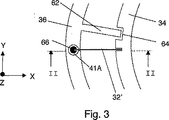
図3は、図1の撓み部分32の好適な構成の簡単ではあるが、より詳細な平面図である。図3の構成の場合には、撓み部分32は、スプリング32’およびベース撓み部分マウント66を備える。図3に示すように、マウント66へのスプリング32’の取付点は、マウント66内に凹状に窪んでいて、同様に、フレーム34に対しても凹状に窪んでいて、マウント66からスプリング32’への、およびフレーム34からスプリング32’への表面応力の伝達を低減している。
FIG. 3 is a simple but more detailed plan view of the preferred configuration of the
ベース撓み部分マウント66は、ベース36の応力から撓み部分32を機械的に絶縁する働きをするベース分離トレンチ41Aで囲まれている。このような応力は、包装および/または接合プロセス、熱膨張等の結果として、キャップ・ウェハ42および基準ウェハ44によりベース36に伝えることができる。図3は、またフレーム溝64と係合しているベース・タブ62も示す。フレーム溝64は、図3に概略的に示すように、ベース・タブ62の幅より若干長いために、フレーム34は、ベース・タブ62がフレーム溝64の壁部に突き当たる前に、ベース36に対してある選択した範囲内だけを回転することができる。この選択した範囲は、選択した範囲内の動きにより撓み部分32が決して損傷を受けないように選択される。このようにして、タブ62と溝64の組合せが、撓み部分32を保護する。
The base
図4の断面図は、撓み部分32の好適な構成の詳細図である。図4は、II線に沿って切断した図3の断面図を含む。II線は、スプリング32’の間近に隣接しているが、スプリングを切断しているわけではなく、これがスプリング32’が図4の断面図として図示されていない理由である。ベース撓み部分マウント66は、キャップ・ウェハ42に固定されていて、接続部46Bを通して基準ウェハ44に連結されている。このようにして、撓み部分32は、キャップ・ウェハ42および基準ウェハ44に連結されていて、ベース36から絶縁されている。このことは有利である。何故なら、キャップ・ウェハ42および基準ウェハ44は、通常、ベース36より遥かに厚く(ジャイロスコープ・ウェハ20の典型的な厚さは50ミクロンにしか過ぎない)、そのため撓み部分32を固定するための機械的剛性が遥かに大きくなるからである。図4は、また、基準分離トレンチ41Cおよびキャップ分離トレンチ41Bも示す。基準分離トレンチ41Cは、基準ウェハ44の頂面(すなわち、ベース36に接合している基準ウェハ44の表面)内に位置しているかもしれない応力から撓み部分32を絶縁する働きをする。同様に、キャップ分離トレンチ41Bは、キャップ・ウェハ42の底面(すなわち、ベース36に接合しているキャップ・ウェハ42の表面)内に位置しているかもしれない応力から、撓み部分32を絶縁する働きをする。図3および図4の湾曲部構成の場合でも、撓み部分32は、スプリング32’およびベース・マウント66を有することが好ましいが、このことは本発明を実行するために必ずそうしなければならないものではない。
The cross-sectional view of FIG. 4 is a detailed view of a preferred configuration of the
図6は、捻れヒンジ26Aおよび曲げヒンジ60の好適な構成の詳細図である、ジャイロスコープ・ウェハ20の一部の概略拡大平面図である。図6に示すように、プレート26は、捻れヒンジ26Aによりフレーム34に取り付けられている。捻れヒンジ26Aの構成は、プレート26が複数の捻れヒンジ26Aの中心を連結している軸を中心にして回転できるようになっている。図6に示すように、捻れヒンジ26Aの長さを増大するために、プレート26内にはスロットが形成されている。このようにスロットが形成されているのは、プレート26の所与の回転を収容するために、捻れヒンジ26A上の必要な歪みを低減するためである。
FIG. 6 is a schematic enlarged plan view of a portion of the
プレート26は、曲げヒンジ60により質量22に連結されている。曲げヒンジ60の構成は、質量26に対してプレート22が傾くことができるようになっている(逆も行われる)。図6に示すように、プレート26に対する質量22の所与の傾斜を収容する目的で、曲げヒンジ60上に必要な歪みを低減するために、曲げヒンジ60の長さを増大するためにスロットが質量22内に形成されている。
The
曲げヒンジ58、56および54の構成は、好適には、図6の曲げヒンジ60の構成に類似していることが好ましい。同様に、好適には、捻れヒンジ28Aおよび30Aの構成は、図6の捻れヒンジ26Aの構成に類似していることが好ましい。図6のヒンジ構成は、本発明の好ましい実施形態に関連する。本発明を実施するために、特定のヒンジ構成を必要とするものではない。
動作
図1および図2の実施形態は、2つの動作モードを有する。第1の好適な動作モードの場合には、質量22および24が振動し、Y方向の角速度を測定するためにフレーム34の運動が感知される。第2の動作モードの場合には、フレーム34が振動し、Y方向の角速度を測定するために質量22および24の運動が感知される。これら2つの方法を順番に考察する。
The configuration of the bending hinges 58, 56 and 54 is preferably similar to that of the bending
Operation The embodiment of FIGS. 1 and 2 has two modes of operation. In the first preferred mode of operation, the
第1の好適な動作モードは、リンク装置を振動するためのアクチュエータを含む。図1および図2の実施形態の場合には、図2の電極48A、48B、50A、50B、52Aおよび52Bが、静電アクチュエータを形成している。電極48A、48B、50A、50B、52Aおよび52Bは、静電相互作用によりプレート30、28および26と相互に作用する。この場合、電極と対応するプレート間の電位差が大きくなると力も増大する。プレート26、28および30は、通常、同じ電位に保持され、一般性を失わないで電位のゼロ基準まで下げることができる。
A first preferred mode of operation includes an actuator for vibrating the linkage. In the embodiment of FIGS. 1 and 2, the
好適には、電極48A、48B、50A、50B、52Aおよび52Bは、図2に示すように、分割電極であることが好ましい。その主な理由は、プレートと電極との間の静電相互作用は、(反発力の代わりに)引力になる傾向があるからである。そのため、どちらかの方向にトルクを提供するために、図2に示すように、回転軸のどちらかの側面上に電極素子が必要になる。好適には、電極48A、48B、50A、50B、52Aおよび52Bと対応するプレート(それぞれ30、28、26)間のギャップは、アクチュエータの運動のための適当な隙間を保持しながら、プレートの所与の回転を得るために必要な電圧をできるだけ低減するために、製造中にギャップの高さdに正確に制御することが好ましい。好適には、電極48A、48B、50A、50B、52Aおよび52Bは、質量22および24、質量22および24の振動を有するプレート26、28および30が形成するリンク装置の振動モードを、Z方向(すなわち、面外方向)において位相が相互に実質的にずれるように励起するには、協力するように電気的に駆動されることが好ましい。図11aおよび図11bは、この振動モードに対応するリンク装置の運動の略図である。
Preferably, the
また好適には、プレート26は、質量22の方向に延びるレバー・アームを含むことが好ましく、プレート30は、質量24の方向に延びるレバー・アームを含むことが好ましく、プレート28は、両方の質量22および24の方向に延びるレバー・アームを含むことが好ましい。図1はこれらすべてを示す。レバー・アームが、プレート26、28および30から延びているために、曲げヒンジ(54,56,58,60)とプレート回転軸(26B,28B,30B)間の距離が増大し、それによりプレートの所与の回転による質量22および24の変位が増大する。このような変位の増大は、ジャイロスコープの性能を改善するために、および/またはより安いコストで所望の性能レベルにするために非常に望ましいことである。質量22および24の増大した行程を収容するために、質量22および24の下の基準ウェハ44内に、凹部45および47がそれぞれ形成される。キャップ・ウェハ42も、ジャイロスコープ・ウェハ20のすべての可動部分を収容するための十分な隙間を有することができるように構成される。
Also preferably, the
ジャイロスコープ・ウェハ20が、角速度wyでY軸を中心にして回転すると、質量22および24は、ジャイロスコープ・ウェハ20の基準フレーム内で振動するX方向のコリオリ力を受ける。質量22および24上のコリオリ力は、X軸に沿って反対方向を向いている。何故なら、2つの質量は、Z軸に沿って反対方向に移動するからである。質量22および24上のコリオリ力は、Z軸を中心にしてフレーム34上に振動トルクを誘起し、これによりフレーム34は角振動を起こす。フレーム34の角振動の振幅は、wyに依存するので(理想的には、振幅はwyに比例することが好ましいが)、この振幅を測定すれば角速度wyを測定することができる。
ジャイロスコープの感度を改善するために、好適には、ジャイロスコープ構造体の機械共振を利用することが好ましい。それ故、好適には、質量22および24を含むリンク装置を、基本的リンク装置共振モード周波数に等しいか、ほぼ等しい周波数で駆動することが好ましい。好適には、基本的リンク装置共振モード(すなわち、最も低い周波数のメカニカル・モード)は、図11aおよび図11bに示すように、質量22および24の逆位相振動に対応することが好ましい。このような対応は、リンク装置およびその支持撓み部分の設計中に確実に行うことができる。駆動周波数をリンク装置の固有周波数のところまたはその近くに選択することにより、所与のアクチュエータ力により供給するリンク装置の運動が増大する。
In order to improve the sensitivity of the gyroscope, it is preferable to use the mechanical resonance of the gyroscope structure. Therefore, it is preferred to drive the link
また、好適には、基本的フレーム共振モードを、確実にZ軸を中心とするフレーム34の剛体角振動に対応させることが好ましい。このことは、フレーム34および撓み部分32を適当に設計することにより行うことができる。さらに、好適には、フレーム基本周波数は、リンク装置の基本周波数より高いことが好ましい。そうすると、確実に、駆動周波数が、周波数において、フレーム34の任意の他の共振モードよりもフレーム34の基本モードに近くなり、それによりジャイロスコープの動作と干渉する恐れがある、フレーム34の高次メカニカル・モードの励起が最小限度まで低減する。
In addition, it is preferable that the basic frame resonance mode should correspond to the rigid body angular vibration of the
この実施形態の場合には、フレーム34の角振動の振幅は、トランスジューサにより感知される。好適には、トランスジューサは、フレーム34およびベース36の間に位置していて、これらフレームおよびベースに連結されている容量性センサであることが好ましい。図5は、このような容量性センサの適当な電極構成を示す。図5の参照番号38A、38Bおよび38Cが示す構成は、木構成と呼ばれ、一方、図5の参照番号40A、40Bおよび40Cが示す構成は、半径構成と呼ばれる。
In this embodiment, the amplitude of the angular vibration of the
木構成の場合、電極38Aはフレーム34に取り付けられ、フレーム34と一緒に移動し、一方、電極38Bおよび38Cは、両方ともベース36に取り付けられていて、フレーム34と一緒に移動しない。1つの電極38A、1つの電極38Bおよび1つの電極38Cからなる「ユニット・セル」は、フレーム34とベース36との間の領域で必要に応じて反復して配置することができる。図5は、2つのこのような「ユニット・セル」を示す。電気的に、すべての電極38Aは、相互に連結されていて、すべての電極38Bは相互に連結されていて、すべての電極38Cは相互に連結されている。それ故、2つのコンデンサ、すなわち、電極38Aと38Bとの間のコンデンサAB、および電極38Aと38Cの間のコンデンサACが形成される。電極38Bが電極38Cに連結されていないこのような配置は、スプリット・フィンガー構成と呼ばれる。フレーム34の運動がコンデンサABおよびACの容量を変えるので、回路でこれらの容量を測定すれば、フレーム34の運動を感知することができる。好適には、このような回路は、基準ウェハ44上に位置することが好ましい。
In the tree configuration,
同様に、半径構成の場合、電極40Aはフレーム34に取り付けられていて、フレーム34と一緒に移動し、一方、電極40Bおよび40Cは、ベース36に取り付けられていて、フレーム34と一緒に移動しない。この場合も、2つのコンデンサが形成され、(好適には、基準ウェハ44上に位置することが好ましい)回路でこれらの容量を測定すれば、フレーム34の運動を感知することができる。
Similarly, in the radial configuration,
第2の動作モードの場合には、フレーム34は、Z軸を中心にして角振動を起こし、この角振動によりX軸に沿って質量22および24の逆位相振動が起こる。ジャイロスコープ・ウェハ20が、角速度wyでY軸を中心にして回転すると、フレーム34の振動が、質量22および24上に振動するZ方向のコリオリ力を誘起する。これにより質量22および24を含むリンク装置が振動する。リンク装置の振動の振幅は、wyに依存するので(理想的には、振幅はwyに比例することが好ましいが)、この振幅を測定すれば角速度wyを測定することができる。
In the second operation mode, the
この第2の動作モードは、第1の好適な動作モードに類似しているので、下記の違いはあっても上記説明を適用することができる。
1)第2の動作モードは、フレーム34を角振動させるためのアクチュエータを含む。フレーム34およびベース36に連結されている静電アクチュエータは、フレーム34を角振動させるための1つの適している手段である。このような静電アクチュエータは、図5の構成を含む種々の電極構成を有することができる。
Since the second operation mode is similar to the first preferred operation mode, the above description can be applied even with the following differences.
1) The second operation mode includes an actuator for angularly vibrating the
2)第2の動作モードの場合、好適には、フレームをその基本共振周波数でまたはその近くの周波数で駆動することが好ましく、また好適には、リンク装置の基本周波数をフレームの基本周波数より高くすることが好ましい。 2) In the case of the second mode of operation, it is preferable to drive the frame at or near its fundamental resonance frequency, and preferably the link device fundamental frequency is higher than the frame fundamental frequency. It is preferable to do.
3)第2の動作モードは、リンク装置の振動を感知するためのトランスジューサを含む。リンク装置に連結されている容量性センサは、適当なトランスジューサである。
図2の電極48A、48B、50A、50B、52Aおよび52Bは、このような容量性センサを供給する。電極52Aおよび52B上のプレート26の運動は、電極52Aとプレート26との間のキャパシタンスを測定することにより、また電極52Bとプレート26との間のキャパシタンスを測定することにより感知される。プレート28および30の運動も同様に感知される。
3) The second mode of operation includes a transducer for sensing the vibration of the link device. A capacitive sensor coupled to the link device is a suitable transducer.
The
両方の動作モードの場合、本発明のある実施形態による角速度センサは、都合のよいことに、センサが受ける任意の線加速度による誤差を低減する。第1の動作モードの場合、感知する運動は、フレーム34の角振動であり、センサの線加速度は、このような運動を誘起する傾向にない。第2の動作モードの場合、感知される運動は、質量22および24の逆位相振動であり、この場合も、感知した運動は、直線加速度を誘起する傾向にある運動ではない。例えば、Z方向の線加速度は、質量22および24の(逆位相とは反対の)同位相の振動を誘起しようとする。
製造
好ましい実施形態の場合には、上記の構造および動作を有する角回転センサ(またはジャイロスコープ)は、(MEMS技術とも呼ばれる)微細加工技術により製造される。2つのタイプのMEMS技術、すなわち、バルクMEMS技術および表面MEMS技術は周知である。バルクMEMS技術は、本発明にとって好適なものである。何故なら、バルクMEMSのプルーフ質量(すなわち、質量22および24)は、より大きな質量を有することができ、表面MEMSのプルーフ質量よりも広い範囲で運動することができるからである。図7a〜図7d、図8a〜図8d、図9a〜図9dおよび図10a、図10bは、本発明の実施形態を製造するのに適している例示としての製造シーケンスの略図である。
For both modes of operation, an angular rate sensor according to an embodiment of the present invention advantageously reduces errors due to any linear acceleration experienced by the sensor. In the first mode of operation, the sensed motion is an angular vibration of the
Manufacturing In the preferred embodiment, the angular rotation sensor (or gyroscope) having the structure and operation described above is manufactured by microfabrication technology (also referred to as MEMS technology). Two types of MEMS technology are well known: bulk MEMS technology and surface MEMS technology. Bulk MEMS technology is preferred for the present invention. This is because the bulk MEMS proof mass (ie,
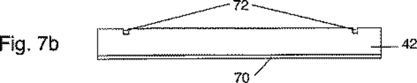
図7a〜図7dは、キャップ・ウェハ42を製造するのに適しているステップのシーケンスの略図である。図7aの場合には、キャップ・ウェハ42は、背面整合マーク72によりパターン形成される。マーク72は、反応性イオン・エッチング(RIE)により形成することができる。図7aから図7bに移動する間に、整合マーク72の反対側のキャップ・ウェハ42の表面が清掃され、次に、酸化物層70を形成するために熱的に酸化される。酸化物層70は、好適には、厚さが約0.5ミクロンであり、水を含む周囲環境で(例えば、1000℃より高い)高温にウェハ42’を加熱することにより作ることができるものであることが好ましい。図7bから図7cに移動する間に、酸化物層70は、図7cに概略示すように、リソグラフィ装置によりパターン形成される。図7cから図7dに移動する間に、酸化物層70により保護されていないキャップ・ウェハ42の材料は、約100ミクロンの深さまでエッチングされる。深RIE(DRIE)は、このステップに適しているエッチング方法である。このプロセス中のこの時点で、キャップ・ウェハ42は、図2に示す構成になる。エッチングの後で、キャップ・ウェハ42は、溶融接合のための準備中に清掃される。適当な清掃ステップは、高温(300℃以上)灰化ステップおよび過酸化硫黄浸漬(sulfuric peroxide dip)ステップを含む。使用する清掃方法は、パターン形成された酸化物層70を無傷のまま残さなければならない。
FIGS. 7 a-7 d are schematic illustrations of a sequence of steps suitable for manufacturing the
図8a〜図8dは、ジャイロスコープ・ウェハ20を製造するにの適している処理ステップのシーケンスの略図である。好適には、ジャイロスコープ・ウェハ20は、プライム低全厚変動(TTV)ウェハであることが好ましい。ジャイロスコープ・ウェハ20は、過酸化硫黄浸漬ステップで清掃され、次に、図8aに示すように、キャップ・ウェハ42上にパターン形成された酸化物層70に溶融接合される。図7〜図10の処理シーケンス中、キャップ・ウェハ42のジャイロスコープ・ウェハ20への接合は、ジャイロスコープ・ウェハ20への基準ウェハ44の接合前の処理の初期段階で行われる。それ故、ジャイロスコープ・ウェハ20へキャップ・ウェハ42を接合するには、共融金属接合、ガラス接合、半田接合、金共融接合、Si−SiO2溶融接合、およびSi−Si溶融接合を含むが、これらに限定されない比較的高温の接合プロセスを使用することが好ましい。図8aから図8bに移動する間に、ジャイロスコープ・ウェハ20の厚さは、通常約500ミクロンの厚さから約400ミクロンの厚さに薄く削られる。従来の研磨方法は、この厚さを薄くするステップを行うのに適している方法である。ジャイロスコープ・ウェハ20は均一に薄くすることもできるし、または質量22および24になるジャイロスコープ・ウェハ20の領域が、ジャイロスコープ・ウェハ20の他の部分より厚くなるように薄くすることもできる。このように厚さを増大すると有利である。何故なら、質量22および24の質量が増大するからである。ジャイロスコープ・ウェハ20を薄くした後で、図8bのスタンドオフ71が、エッチングの前のリソグラフィ装置によるパターン形成により形成される。KOHエッチングがこのステップに適している。スタンドオフ71の目的は、図2の電極48A、B、50A、Bおよび52A、Bのようなアクチュエータの電極と、対応するプレート(すなわち、それぞれプレート30、28および26)との間の垂直方向の分離dを正確に決定することである。
FIGS. 8 a-8 d are schematic diagrams of a sequence of processing steps suitable for manufacturing the
図8bから図8cに移動する間に、パターン形成された層46’がジャイロスコープ・ウェハ20上に堆積する。好適には、パターン形成された層46’は、堆積され、次に、(例えば、リソグラフィおよびその後のエッチングにより)パターン形成されるGe層であることが好ましい。好適には、パターン形成された層46’も、図5に示すタイプであってもよい電極をフレーム34とベース36間に形成することが好ましい。別の方法としては、フレーム34とベース36との間の電極は、パターン形成された層46’の堆積とは別の処理ステップで形成することができる。
While moving from FIG. 8 b to FIG. 8 c, a patterned
図8cから図8dに移動する間に、ジャイロスコープ・ウェハ20の機械素子が、ジャイロスコープ・ウェハ20を貫通するエッチングにより形成される。エッチングするパターンは、フォトリソグラフィにより形成することができる。酸化物層70上で止まるこのエッチングの場合には、2ミクロンのライン幅と2ミクロンの間隔が適している。シリコン・オン・インシュレータ(SOI)アンチフッティング改善による深いRIEがこのステップに適しているエッチング方法である。好適には、このエッチングは、高アスペクト比のフィーチャを生成するのに適しているエッチング・プロセスで実行することが好ましい。図8dのエッチングを実行した後で、図1〜図4および図6に示すジャイロスコープ・ウェハ20のすべての機械素子が形成される。これらの素子としては、質量22および24、プレート26、28および30、撓み部分32、フレーム34、およびヒンジ26A、28A、30A、54、56、58および60等がある。図を分かりやすくするために、図8dにはプレート28と質量22および24だけを示す。
While moving from FIG. 8 c to FIG. 8 d, the mechanical elements of the
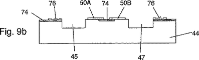
図9a〜図9bは、基準ウェハ44を製造するのに適している処理ステップのシーケンスの略図である。図9aの場合には、参照番号74は基準ウェハ44の能動エリアの略図を示す。能動エリア74は、ジャイロスコープ・ウェハ20、およびジャイロスコープ・ウェハ20を駆動するための回路、およびジャイロスコープ・ウェハ20が供給する出力信号を感知するための回路に電気的に接触する領域を含む。好適には、このような回路は、従来のシリコンCMOS回路であることが好ましい。好ましい実施形態の場合には、従来のCMOSプロセス中に堆積される金属の最後の層は、接合金属として使用するのに適している金属層である。金属のこの上部層も、電極48A、B、50A、Bおよび52A、B(図9bには、電極50A、Bだけを図示してある)、および図9aに概略を示す接合パッド76を形成する。図9aから図9bに移動する間に、基準ウェハ44内に凹部45および47が形成される。好適には、凹部45および47は、DRIEにより約100ミクロンの深さに形成することが好ましい。
FIGS. 9 a-9 b are schematic diagrams of a sequence of processing steps that are suitable for manufacturing the
図10a〜図10bは、ジャイロスコープ・ウェハ20、基準ウェハ44およびキャップ・ウェハ42の最終組立に適している処理ステップのシーケンスの略図である。図10aの場合には、基準ウェハ44は、ジャイロスコープ・ウェハ20上のパターン形成された層46’と基準ウェハ44上の接合パッド76との間の整合している金属−金属接合を通して、ジャイロスコープ・ウェハ20に取り付けられている。図7〜図10の処理シーケンス中に、ジャイロスコープ・ウェハ20への基準ウェハ44の接合が、ジャイロスコープ・ウェハ20へのキャップ・ウェハ42の接合より後の処理段階で行われる。それ故、ジャイロスコープ・ウェハ20への基準ウェハ44の接合は、共融金属接合、アルミニウム−ゲルマニウム接合、半田接合、インジウム−金接合、およびポリマー結合を含むが、これらに限定されない比較的低温の接合プロセスにより行うことが好ましい。
FIGS. 10 a-10 b are schematic diagrams of a sequence of processing steps suitable for final assembly of the
図10aのプレート28と電極50Aおよび50B間の間隔dは、スタンドオフ71およびパターン形成された層46’の厚さの合計により決まり、スタンドオフ71の高さを選択することにより正確に制御(または予め決定)することができる。他の電極(例えば、電極48A、B、および電極52A、B)と、対応するプレート(例えば、各プレート30および26)との間の間隔も、同じ方法で決まり、通常、すべてのプレートとその対応する電極との間の間隔は同じ所定の間隔dになる。図7〜図10の処理シーケンスでは、プレートと電極との間に間隔を形成するために、ジャイロスコープ・ウェハ20上だけでスタンドオフ71が形成されているが、基準ウェハ44上だけ、またはジャイロスコープ・ウェハ20および基準ウェハ44両方上でスタンドオフを形成することもできる。図10aから図10bに移動する間に、上方から能動エリア74にアクセスすることができるように、材料をキャップ・ウェハ42からエッチングにより除去することができる。上方から能動エリア74にアクセスすることができるようにすることにより、図10bの角速度センサへの電気的接続が容易になる。
The spacing d between the
好適には、基準ウェハ44は、密封状態にすることができる金属−金属接合を通して、ジャイロスコープ・ウェハ20に取り付けることが好ましい。同様に、好適には、ジャイロスコープ・ウェハ20は、同様に密封状態にすることができる溶融接合により、キャップ・ウェハ42に取り付けることが好ましい。その結果、基準ウェハ44、ジャイロスコープ・ウェハ20およびキャップ・ウェハ42のアセンブリ全体は、ジャイロスコープ素子(質量22および24など)と周囲の環境との間に密封バリアを供給することができる。
Preferably, the
ジャイロスコープの異なる市場のいくつかの性能仕様に適合するために、ある場合には、密封バリアが形成するエンクロージャ内に、低圧(例えば、大気圧よりかなり低い約1mTorr)を供給すると有利である。このようにして、エンクロージャを満たしている空気(または他の気体)による質量22および24の運動に対する抵抗を必要に応じて低減することができる。別の方法としては、運動への空気抵抗を低減するために、質量22および24内(およびリンク装置の他の可動部分内)に孔部を設けることもできる。ほかの場合には、大気圧より高い圧力を密封エンクロージャ内に供給するのが望ましい場合もある。
In order to meet several performance specifications in different markets for gyroscopes, in some cases it may be advantageous to provide a low pressure (eg, about 1 mTorr well below atmospheric pressure) within the enclosure formed by the hermetic barrier. In this way, the resistance to movement of the
図7a〜図7d、図8a〜図8d、図9a〜図9bおよび図10a〜図10bのこの説明は、本発明の好ましい実施形態を製造するのに適している、例示としての処理ステップのシーケンスの概要を説明するためのものである。それ故、上記1つのステップが、本発明を実行するのに不可欠なものであるのではない。さらに、上記ステップの大部分は、上記以外の他の方法であるが、半導体処理業界では周知の方法により実行することができる。より一般的な言い方をすると、詳細な説明全体は、ほとんど例示としてのものであって、本発明を制限するものではない。本発明の実施形態の他の例について以下に簡単に説明する。 This description of FIGS. 7a-7d, 8a-8d, 9a-9b, and 10a-10b is an exemplary sequence of processing steps that is suitable for manufacturing a preferred embodiment of the present invention. It is for explaining the outline of the. Therefore, the above one step is not essential for carrying out the present invention. Furthermore, most of the steps are other methods than those described above, but can be performed by methods well known in the semiconductor processing industry. In more general terms, the entire detailed description is merely exemplary and is not intended to limit the invention. Another example of the embodiment of the present invention will be briefly described below.
図12は、他の電極構成の概略平面図である。図12の場合には、質量22および24、およびプレート26、28および30は図示していない。そのためリンク装置のこれらの素子の下の電極を見ることができる。図12の構成の場合には、電極48A、B、50A、Bおよび52A、Bは、すでに説明したように、それぞれプレート30、28および26を駆動するためのものである。さらに、図12の構成は、質量の運動、またはより一般的な言い方をすると、リンク装置の運動を感知するための電極51Aおよび51Bを提供する。電極51Aおよび51Bが供給する信号は、リンク装置アクチュエータを駆動する回路により有利に使用することができる。例えば、このようにリンク装置の運動を感知することにより、駆動回路は、その基本的な機械共振周波数でリンク装置を正確に駆動することができる。
FIG. 12 is a schematic plan view of another electrode configuration. In the case of FIG. 12, the
図13は、本発明のある実施形態による集積二重軸ジャイロスコープの概略平面図である。図13の構成の場合には、好適には、Y軸サブセンサ20YおよびX軸サブセンサ20Xは、1つのシリコン・チップ21上に形成するのが好ましい。好適には、サブセンサ20Xおよび20Yは、図1および図2のところで説明したセンサであることが好ましく、図13の構成は、集積角速度センサにより二重軸感知を行うことが好ましい。このように集積することにより、2つの非集積型の単一軸センサと比較した場合、コストが大幅に低減する。
FIG. 13 is a schematic plan view of an integrated dual axis gyroscope according to an embodiment of the present invention. In the case of the configuration of FIG. 13, it is preferable that the Y-
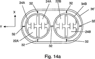
図14aおよび図14bは、望ましくない運動の共通モード拒否を行う本発明のある実施形態の概略平面図である。図14aおよび図14bの構成は、2つのフレーム、すなわちフレーム34Aおよびフレーム34Bを含む。質量22および24が図1のフレーム34内に位置するのとほぼ同じように、質量22Aおよび24Aは、フレーム34A内に位置していて、質量22Bおよび24Bはフレーム34B内に位置する。図14aおよび図14bの質量22A、Bおよび24A、Bは、質量24Aおよび22Bが同位相になるように振動する。質量22Aおよび24Aは、質量22Bおよび24Bのように、位相からずれるようにリンクしている。
Figures 14a and 14b are schematic plan views of an embodiment of the present invention that provides common mode rejection of undesirable movement. The configuration of FIGS. 14a and 14b includes two frames, namely frame 34A and frame 34B. Just as
フレーム34Aおよび34Bは、撓み部分32により相互に連結されていて、複数の撓み部分32によりベース36’に連結されている。図14aおよび図14bの撓み部分の構成は例示としてのものであって、本発明は他の撓み部分構成によっても実行することができる。撓み部分32によるフレーム34Aとフレーム34Bとの接続は、フレーム34Aおよび34Bの位相ずれ回転に対してフレーム34Aおよび34Bの同位相回転を阻止する傾向がある。何故なら、フレーム34Aおよび34Bの同位相回転は、同じ大きさの位相ずれ回転よりも大きく撓み部分32を延ばすからである。
The
図14aのセンサが、図14aのY軸を中心にして回転すると(または図14bのセンサが、図14bのY軸を中心にして回転すると)、フレーム34Aおよび34Bに加わるZ方向のトルクは位相からずれる。その理由は、フレーム34Aおよび34B内の2つのリンク装置が、相互に位相からずれるように運動するからである。対照的に、Z軸を中心とする図14aおよび図14bのセンサの角加速度は、フレーム34Aおよび34Bを同位相で回転させる。それ故、図14aおよび図14bのセンサは、Z軸を中心とする角加速度による偽の信号を拒否することができる。これは図1の実施形態が有していない機能である。図14aおよび図14bのフレーム34Aおよび34Bの回転は、(例えば、容量性センサにより)上記のように感知することができる。
When the sensor of FIG. 14a rotates about the Y axis of FIG. 14a (or when the sensor of FIG. 14b rotates about the Y axis of FIG. 14b), the torque in the Z direction applied to the
さらに、図14aおよび図14bの実施形態は、被駆動リンク装置内にゼロの正味の線形および角運動量を有し、一方、図1の実施形態は、被駆動リンク装置内にゼロの正味の線形運動量を有するが、ゼロでない正味の角運動量を有する。センサ・パッケージへの振動の伝導は、被駆動リンク装置がゼロの正味の線形または角運動量を有している場合には、低減する傾向があるので、図14aおよび図14bの実施形態は、図1の実施形態と比較した場合、供給するパッケージ振動は小さいものでなければならない。振動が小さいと、バイアス誤差および象限誤差のような測定誤差が小さくなる。 Further, the embodiment of FIGS. 14a and 14b has zero net linearity and angular momentum in the driven link device, while the embodiment of FIG. 1 has zero net linearity in the driven link device. Has momentum but non-zero net angular momentum. Since the conduction of vibrations to the sensor package tends to decrease if the driven linkage has zero net linear or angular momentum, the embodiment of FIGS. Compared to one embodiment, the supplied package vibration must be small. When the vibration is small, measurement errors such as bias error and quadrant error are small.
図14aおよび図14bの実施形態が提供するZ方向の角加速度の共通モード拒否の利点を最大にするためには、好適には、フレーム34Aおよび34Bは、ほぼ同じ形を有することが好ましく、フレーム34Aおよび34B内のリンク装置は、ほぼ同じ構成および向きを有することが好ましい。対称をこのレベルにすることにより、Y方向の角速度に応じない運動(例えば、Z方向の角加速度による運動)の拒否を最大にする、ほぼ等しく反対方向であるY方向の角速度に応じる運動が生じる。
In order to maximize the advantages of the common mode rejection of angular acceleration in the Z direction provided by the embodiment of FIGS. 14a and 14b, it is preferred that the
図15は、フレーム34およびベース36が円形ではなく矩形の形をしている本発明の他の実施形態の略図である。図1の実施形態と同様に、図15のフレーム34内には、質量22および24がプレート26、28および30により一緒に連結されている。また、図1の実施形態のように、質量22および24、およびプレート26、28および30を含むリンク装置は、好適には、(図15には図示していない)静電アクチュエータにより振動することが好ましい。Y軸を中心にして図15の実施形態が回転すると、質量22および24上にX方向のコリオリ力が生じる。フレーム34は、フレーム34をベース36に対して移動させることができる複数の撓み部分32によりベース36と連結されている。Y軸を中心にするセンサの角速度に応じた質量22および24上のX方向のコリオリ力は、X方向にフレーム34をベース36に対して移動させようとする。フレーム34とベース36との間の相対運動は、好適には、図15に略図で示す容量性センサ100により感知することが好ましい。
FIG. 15 is a schematic illustration of another embodiment of the present invention in which the
図15のフレーム34および撓み部分32の構成は、フレーム34の回転全体を禁止し、Y方向の角速度に対するフレーム34のX方向の変形を感知する。(例えば、フレーム34の硬度をさらに硬くして)X方向の変形を禁止し、フレーム34の回転を感知する、図15のフレーム34と撓み部分32の他の構成も使用することができる。
The configuration of the
図16aおよび図16bは、フレーム34とベース36との間の撓み部分32の他の構成のいくつかの例を示す。図16aは、図1の撓み部分32の配置に対して45度回転した撓み部分32の配置である。図16bは、フレーム34とベース36との間に対称的に位置している3つの撓み部分32の配置である。もちろん、感知する角速度に応じてベース36に対してフレーム34が移動することができるフレーム34とベース36との間の撓み部分の任意の配置により本発明を実行することができる。
FIGS. 16 a and 16 b show some examples of other configurations of the
本発明の実施形態の上記詳細な説明においては、静電アクチュエータであるリンク装置を振動させるためのアクチュエータについて説明した。リンク装置を振動させるための他のアクチュエータとしては、電磁アクチュエータ、圧電アクチュエータおよび熱アクチュエータ等があるが、これらに限定されない。また、上記説明においては、容量性センサであるフレーム34の角振動を感知するためのトランスジューサについて説明した。フレーム34の角振動を感知するための他のトランスジューサとしては、電磁センサ、ピエゾ抵抗センサおよび圧電センサ等があるが、これらに限定されない。
In the detailed description of the embodiment of the present invention, the actuator for vibrating the link device which is an electrostatic actuator has been described. Other actuators for vibrating the link device include, but are not limited to, electromagnetic actuators, piezoelectric actuators, and thermal actuators. In the above description, the transducer for sensing the angular vibration of the
本発明の実施形態の上記詳細な説明においては、静電アクチュエータである、フレーム34を角振動させるためのアクチュエータについて説明した。フレーム34を振動させるための他のアクチュエータとしては、電磁アクチュエータ、圧電アクチュエータおよび熱アクチュエータ等があるが、これらに限定されない。また、上記説明においては、容量性センサであるリンク装置の振動を感知するためのトランスジューサについて説明した。リンク装置の振動を感知するための他のトランスジューサとしては、電磁センサ、ピエゾ抵抗センサおよび圧電センサ等があるが、これらに限定されない。
In the detailed description of the embodiment of the present invention, an actuator for angularly vibrating the
Claims (78)
a)感知サブアセンブリであって、
i)前記面に平行で平らなフレームと、
ii)前記面内に配置されている第1の質量と、
iii)前記第1の質量とともに前記面内に配置されている第2の質量と、
iv)前記フレーム内に位置し、前記フレームに連結されているリンク装置であって、前記リンク装置は、前記第1の質量および前記第2の質量に連結され、前記リンク装置は、前記第1および第2の質量が、前記面に垂直にそれぞれ反対方向に移動するのを許容するリンク装置とを備える感知サブアセンブリと、
b)前記リンク装置及び前記フレームの一方を駆動周波数で振動させるためのアクチュエータと、
c)前記角速度により前記リンク装置及び前記フレームの他方の運動を感知するためのトランスジューサとを備えるセンサ。A sensor for measuring an angular velocity of a sensor surface, wherein the sensor is
a) a sensing subassembly comprising:
i) a flat frame parallel to the surface;
ii) a first mass disposed in the plane;
iii) a second mass disposed in the plane along with the first mass;
iv) A link device located in the frame and connected to the frame, wherein the link device is connected to the first mass and the second mass, and the link device is connected to the first mass A sensing subassembly comprising: and a linking device that allows the second mass to move in respective opposite directions perpendicular to the plane;
b) an actuator for vibrating one of the link device and the frame at a driving frequency;
c) A sensor comprising a transducer for sensing the other movement of the link device and the frame according to the angular velocity.
前記フレームに連結され、また前記第1および第2の質量におよびその間に連結されたセンター・プレートであって、回転の中心軸を中心にして回転可能なセンター・プレートと、
前記フレームおよび前記第1の質量に連結された第1の縁部プレートであって、回転の第1の軸を中心にして回転可能な第1の縁部プレートと、
前記フレームおよび前記第2の質量に連結されている第2の縁部プレートであって、回転の第2の軸を中心にして回転可能な第2の縁部プレートとをさらに備え、
回転の前記中心軸、第1および第2の軸が相互に平行であり、また前記センサ面に平行である請求項1に記載のセンサ。The link device is
A center plate coupled to the frame and coupled to and between the first and second masses, the center plate being rotatable about a central axis of rotation;
A first edge plate coupled to the frame and the first mass, the first edge plate being rotatable about a first axis of rotation;
A second edge plate coupled to the frame and the second mass, the second edge plate being rotatable about a second axis of rotation;
The sensor of claim 1, wherein the central axis of rotation, the first and second axes are parallel to each other and parallel to the sensor surface.
前記フレームに連結され、また前記第1および第2の質量におよびその間に連結されたセンター・プレートであって、回転の中心軸を中心にして回転可能なセンター・プレートと、
前記フレームおよび前記第1の質量に連結されている第1の縁部プレートであって、回転の第1の軸を中心にして回転可能な第1の縁部プレートと、
前記フレームおよび前記第2の質量に連結されている第2の縁部プレートであって、回転の第2の軸を中心にして回転可能な第2の縁部プレートとをさらに備え、
回転の前記中心軸、第1および第2の軸が相互に平行であり、また前記センサ面に平行である請求項19に記載のセンサ。The link device is
A center plate coupled to the frame and coupled to and between the first and second masses, the center plate being rotatable about a central axis of rotation;
A first edge plate coupled to the frame and the first mass, the first edge plate being rotatable about a first axis of rotation;
A second edge plate coupled to the frame and the second mass, the second edge plate being rotatable about a second axis of rotation;
20. A sensor according to claim 19, wherein the central axis of rotation, the first and second axes are parallel to each other and parallel to the sensor surface.
前記基準ウェハの前記頂面上の前記第1の縁部プレートの下に位置し、所定の距離dだけ前記第1の縁部プレートから離れている第1の縁部分割電極と、
前記基準ウェハの前記頂面上の前記第2の縁部プレートの下に位置し、前記距離dだけ前記第2の縁部プレートから離れている第2の縁部分割電極と、
前記基準ウェハの前記頂面上の前記センター・プレートの下に位置し、前記距離dだけ前記センター・プレートから離れているセンター分割電極とを備える請求項20に記載のセンサ。The actuator is
A first edge segmented electrode located below the first edge plate on the top surface of the reference wafer and spaced from the first edge plate by a predetermined distance d;
A second edge segmented electrode located below the second edge plate on the top surface of the reference wafer and separated from the second edge plate by the distance d;
21. The sensor according to claim 20, further comprising a center split electrode located below the center plate on the top surface of the reference wafer and spaced from the center plate by the distance d.
A)角速度のX成分を測定するための第1のサブセンサを備え、前記第1のサブセンサが、
a)第1の感知サブアセンブリであって、
i)前記面に平行で平らな第1のフレームと、
ii)前記面内に配置される第1の質量と、
iii)前記第1の質量とともに前記面内に配置される第2の質量と、
iv)前記フレーム内に位置し、前記フレームに連結された第1のリンク装置であって、前記第1の質量および前記第2の質量に連結され、前記第1および第2の質量がそれぞれ前記面に垂直な反対方向に移動するのを許容する第1のリンク装置とを備える第1の感知サブアセンブリと、
b)駆動周波数で前記第1のリンク装置及び前記第1のフレームの一方を振動するための第1のアクチュエータと、
c)角速度のX成分による前記第1のリンク装置及び前記第1のフレームの他方の運動を感知するための第1のトランスジューサとを備え、さらに、
B)角速度のY成分を測定するための第2のサブセンサを備え、前記第2のサブセンサが、
a)第2の感知サブアセンブリであって、
i)前記面に平行で平らな第2のフレームと、
ii)前記面内に配置される第3の質量と、
iii)前記第3の質量とともに前記面内に配置される第4の質量と、
iv)前記第2のフレーム内に位置し、前記第2のフレームに連結された第2のリンク装置であって、前記第3の質量および前記第4の質量に連結され、前記第3および第4の質量が前記面に垂直な反対方向に移動するのを許容する第2のリンク装置とを備える第2の感知サブアセンブリと、
b)駆動周波数で前記第2のリンク装置及び前記第2のフレームの一方を振動するための第2のアクチュエータと、
c)角速度のY成分による前記第2のリンク装置及び前記第2のフレームの他方の運動を感知するための第2のトランスジューサとを備えるセンサ。A biaxial sensor for measuring the X and Y components of the angular velocity of the XY sensor surface, the biaxial sensor comprising:
A) comprising a first subsensor for measuring the X component of the angular velocity, wherein the first subsensor comprises:
a) a first sensing subassembly, comprising:
i) a first frame parallel to and flat with said plane;
ii) a first mass disposed in the plane;
iii) a second mass disposed in the plane along with the first mass;
iv) a first link device located in the frame and connected to the frame, wherein the first link device is connected to the first mass and the second mass, and the first and second masses are respectively A first sensing subassembly comprising a first linkage that allows movement in an opposite direction perpendicular to the surface;
b) a first actuator for vibrating one of the first link device and the first frame at a drive frequency;
c) a first transducer for sensing movement of the first link device and the other of the first frame due to an X component of angular velocity; and
B) comprising a second subsensor for measuring the Y component of the angular velocity, wherein the second subsensor comprises:
a) a second sensing subassembly, comprising:
i) a second frame parallel to and flat with said plane;
ii) a third mass disposed in the plane;
iii) a fourth mass disposed in the plane along with the third mass;
iv) a second link device located in the second frame and connected to the second frame, wherein the second link device is connected to the third mass and the fourth mass; A second sensing subassembly comprising a second linkage that allows a mass of 4 to move in an opposite direction perpendicular to said plane;
b) a second actuator for vibrating one of the second link device and the second frame at a drive frequency;
c) A sensor comprising a second transducer for sensing movement of the second link device and the other of the second frame due to a Y component of angular velocity.
a)第1の感知サブアセンブリであって、
i)前記面に平行で平らな第1のフレームと、
ii)前記面内に配置される第1の質量と、
iii)前記第1の質量とともに前記面内に配置される第2の質量と、
iv)前記フレーム内に位置し、前記フレームに連結された第1のリンク装置であって、前記第1の質量および前記第2の質量に連結され、前記第1および第2の質量がそれぞれ前記面に垂直な反対方向に移動するのを許容する第1のリンク装置とを備える第1の感知サブアセンブリと、
b)駆動周波数で前記第1のリンク装置及び前記第1のフレームの一方を振動するための第1のアクチュエータと、
c)前記角速度に応じた前記第1のリンク装置及び前記第1のフレームの他方の第1の運動を感知するための第1のトランスジューサと、
d)第2の感知サブアセンブリであって、
i)前記面に平行で平らな第2のフレームと、
ii)前記面内に配置される第3の質量と、
iii)前記第3の質量とともに前記面内に配置される第4の質量と、
iv)前記第2のフレーム内に位置し、前記第2のフレームに連結された第2のリンク装置であって、前記第3の質量および前記第4の質量に連結され、前記第3および第4の質量がそれぞれ前記面に垂直な反対方向に移動するのを許容し、前記第1のリンク装置と同じ構成および向きを有していて、前記第3の質量が前記第1の質量に対応し、前記第4の質量が前記第2の質量に対応する第2のリンク装置とを備える第2の感知サブアセンブリと、
e)駆動周波数で前記第2のリンク装置及び前記第2のフレームの一方を振動するための第2のアクチュエータと、
f)前記角速度に応じた前記第2のリンク装置及び前記第2のフレームの他方の第2の運動を感知するための第2のトランスジューサとを備え、
前記第1および第2のトランスジューサからの信号が、前記角速度に応じた前記第1および第2の運動を、前記角速度によらない運動から区別するために結合されるセンサ。A sensor for measuring an angular velocity of a sensor surface, wherein the sensor is
a) a first sensing subassembly, comprising:
i) a first frame parallel to and flat with said plane;
ii) a first mass disposed in the plane;
iii) a second mass disposed in the plane along with the first mass;
iv) a first link device located in the frame and connected to the frame, wherein the first link device is connected to the first mass and the second mass, and the first and second masses are respectively A first sensing subassembly comprising a first linkage that allows movement in an opposite direction perpendicular to the surface;
b) a first actuator for vibrating one of the first link device and the first frame at a drive frequency;
c) a first transducer for sensing the first movement of the other of the first link device and the first frame in response to the angular velocity;
d) a second sensing subassembly, comprising:
i) a second frame parallel to and flat with said plane;
ii) a third mass disposed in the plane;
iii) a fourth mass disposed in the plane along with the third mass;
iv) a second link device located in the second frame and connected to the second frame, wherein the second link device is connected to the third mass and the fourth mass; 4 masses are allowed to move in opposite directions perpendicular to the plane, have the same configuration and orientation as the first link device, and the third mass corresponds to the first mass And a second sensing subassembly comprising a second linkage wherein the fourth mass corresponds to the second mass;
e) a second actuator for vibrating one of the second link device and the second frame at a drive frequency;
f) a second transducer for sensing the second movement of the second link device according to the angular velocity and the other second movement of the second frame;
A sensor in which signals from the first and second transducers are coupled to distinguish the first and second motions in response to the angular velocity from motions that are not dependent on the angular velocity.
a)ジャイロスコープ・ウェハから感知サブアセンブリをエッチングするステップであって、前記サブアセンブリが、
i)前記面に平行で平らなフレームと、
ii)前記フレームに連結されたリンク装置であって、前記面内に配置され、前記面に垂直な反対方向へのそれぞれの移動が許容された第1の質量および第2の質量を備えたリンク装置とを備えるステップと、
b)駆動周波数で前記リンク装置及び前記フレームの一方を振動するためのアクチュエータを提供するステップと、
c)前記角速度に応じた前記リンク装置及び前記フレームの他方の運動を感知するためのトランスジューサを提供するステップとを含む方法。A method for manufacturing a sensor for measuring the angular velocity of a sensing surface, the method comprising:
a) etching a sensing subassembly from a gyroscope wafer, the subassembly comprising:
i) a flat frame parallel to the surface;
ii) A link device connected to the frame, the link device having a first mass and a second mass arranged in the plane and allowed to move in opposite directions perpendicular to the plane. An apparatus comprising:
b) providing an actuator for vibrating one of the link device and the frame at a drive frequency;
c) providing a transducer for sensing movement of the link device and the other of the frame in response to the angular velocity.
基準ウェハの頂面に前記ベースを基準接合するステップとをさらに含み、
アクチュエータを提供する前記ステップが、前記基準ウェハの前記頂面上に複数の電極を堆積するステップを含み、
トランスジューサを提供する前記ステップが、前記フレームに連結されているフレーム電極を堆積するステップと、前記ベースに連結されているベース電極を堆積するステップとを含み、前記フレームおよびベース電極が容量性センサを備える請求項40に記載の方法。Etching a flat base from the gyroscope wafer, the base being parallel to the frame and positioned around the frame;
Further comprising the step of reference bonding the base to the top surface of a reference wafer;
Providing the actuator comprises depositing a plurality of electrodes on the top surface of the reference wafer;
Providing a transducer includes depositing a frame electrode coupled to the frame and depositing a base electrode coupled to the base, the frame and the base electrode comprising a capacitive sensor. 41. The method of claim 40, comprising.
前記フレームに連結され、また前記第1および第2の質量におよびその間に連結されているセンター・プレートをエッチングするステップと、
前記フレームおよび前記第1の質量に連結されている第1の縁部プレートをエッチングするステップと、
前記フレームおよび前記第2の質量に連結されている第2の縁部プレートをエッチングするステップとをさらに含み、
前記プレートが、前記センサ面に平行な、平行回転軸を中心にして回転することができ、
前記リンク装置が、前記センター・プレートと、前記第1および第2の縁部プレートとをさらに備える請求項51に記載の方法。The step of etching the sensing subassembly comprises:
Etching a center plate coupled to the frame and coupled to and between the first and second masses;
Etching a first edge plate coupled to the frame and the first mass;
Etching a second edge plate coupled to the frame and the second mass;
The plate can rotate about a parallel axis of rotation parallel to the sensor surface;
52. The method of claim 51, wherein the linkage further comprises the center plate and the first and second edge plates.
前記センター・プレートを前記フレームに連結している撓み部分の第1のペアをエッチングするステップと、
前記第1の縁部プレートを前記フレームに連結している撓み部分の第2のペアをエッチングするステップと、
前記第2の縁部プレートを前記フレームに連結している撓み部分の第3のペアをエッチングするステップとをさらに含む請求項57に記載の方法。The step of etching the sensing subassembly comprises:
Etching a first pair of flexures connecting the center plate to the frame;
Etching a second pair of flexures connecting the first edge plate to the frame;
58. The method of claim 57, further comprising: etching a third pair of flexures connecting the second edge plate to the frame.
前記基準ウェハの前記頂面上の前記第1の縁部プレートの下に位置し、所定の距離(d)だけ前記第1の縁部プレートから分離している第1の縁部分割電極を堆積するステップと、
前記基準ウェハの前記頂面上の前記第2の縁部プレートの下に位置し、前記距離(d)だけ前記第2の縁部プレートから分離している第2の縁部分割電極を堆積するステップと、
前記基準ウェハの前記頂面上の前記センター・プレートの下に位置し、前記距離(d)だけ前記センター・プレートから分離しているセンター分割電極を堆積するステップとを含む請求項57に記載の方法。The step of depositing a plurality of control electrodes comprises:
Depositing a first edge-dividing electrode located below the first edge plate on the top surface of the reference wafer and separated from the first edge plate by a predetermined distance (d); And steps to
Depositing a second edge-dividing electrode located below the second edge plate on the top surface of the reference wafer and separated from the second edge plate by the distance (d); Steps,
58. depositing a center split electrode located below the center plate on the top surface of the reference wafer and separated from the center plate by the distance (d). Method.
前記ベースから前記撓み部分を分離している複数のベース分離トレンチをエッチングするステップとをさらに含み、
それにより前記ベースの応力が前記撓み部分に伝わらない請求項51に記載の方法。Etching a plurality of flexures connecting the frame to the reference wafer;
Etching a plurality of base isolation trenches separating the flexible portion from the base;
52. The method of claim 51, whereby stress in the base is not transferred to the flexure.
それにより前記基準ウェハの前記頂面の応力が前記撓み部分に伝わらない請求項68に記載の方法。Etching a plurality of reference isolation trenches separating the flexible portion from the top surface of the reference wafer;
69. The method of claim 68, whereby stress on the top surface of the reference wafer is not transferred to the flexure.
前記ベースから前記撓み部分を分離する複数のベース分離トレンチをエッチングするステップとをさらに含み、
それにより前記ベースの応力が前記撓み部分に伝わらない請求項記70載の方法。Etching a plurality of flexures connecting the frame to the cap wafer;
Etching a plurality of base isolation trenches that isolate the flexure from the base;
71. A method according to claim 70, wherein stress of the base is not transmitted to the bent portion.
Applications Claiming Priority (3)
| Application Number | Priority Date | Filing Date | Title |
|---|---|---|---|
| US10/690,224 US6892575B2 (en) | 2003-10-20 | 2003-10-20 | X-Y axis dual-mass tuning fork gyroscope with vertically integrated electronics and wafer-scale hermetic packaging |
| US10/690,224 | 2003-10-20 | ||
| PCT/US2004/034431 WO2005043079A2 (en) | 2003-10-20 | 2004-10-12 | X-y axis dual-mass tuning fork gyroscope with vertically integrated electronics and wafer-scale hermetic packaging |
Publications (3)
| Publication Number | Publication Date |
|---|---|
| JP2007509346A JP2007509346A (en) | 2007-04-12 |
| JP2007509346A5 JP2007509346A5 (en) | 2007-05-31 |
| JP5021312B2 true JP5021312B2 (en) | 2012-09-05 |
Family
ID=34521583
Family Applications (1)
| Application Number | Title | Priority Date | Filing Date |
|---|---|---|---|
| JP2006536699A Expired - Fee Related JP5021312B2 (en) | 2003-10-20 | 2004-10-12 | Angular velocity sensor and manufacturing method thereof |
Country Status (5)
| Country | Link |
|---|---|
| US (1) | US6892575B2 (en) |
| EP (1) | EP1676096B1 (en) |
| JP (1) | JP5021312B2 (en) |
| TW (1) | TWI247896B (en) |
| WO (1) | WO2005043079A2 (en) |
Families Citing this family (119)
| Publication number | Priority date | Publication date | Assignee | Title |
|---|---|---|---|---|
| US7458263B2 (en) * | 2003-10-20 | 2008-12-02 | Invensense Inc. | Method of making an X-Y axis dual-mass tuning fork gyroscope with vertically integrated electronics and wafer-scale hermetic packaging |
| KR100652952B1 (en) * | 2004-07-19 | 2006-12-06 | 삼성전자주식회사 | The MEMS gyroscope with coupling spring |
| FR2876180B1 (en) * | 2004-10-06 | 2006-12-08 | Commissariat Energie Atomique | RESONATOR WITH OSCILLATING MASSES. |
| FI116544B (en) * | 2004-12-31 | 2005-12-15 | Vti Technologies Oy | Oscillating, micro-mechanical angular velocity sensor has stationary electrode pairs together with surface of mass forming two capacitance which varies as function of angle of rotation of primary motion of mass |
| FI116543B (en) * | 2004-12-31 | 2005-12-15 | Vti Technologies Oy | Oscillating micro-mechanical angular velocity sensor, for vehicle, has seismic masses that are connected to support areas using springs or auxiliary structures |
| US7442570B2 (en) | 2005-03-18 | 2008-10-28 | Invensence Inc. | Method of fabrication of a AL/GE bonding in a wafer packaging environment and a product produced therefrom |
| US7240552B2 (en) * | 2005-06-06 | 2007-07-10 | Bei Technologies, Inc. | Torsional rate sensor with momentum balance and mode decoupling |
| US7621183B2 (en) * | 2005-11-18 | 2009-11-24 | Invensense Inc. | X-Y axis dual-mass tuning fork gyroscope with vertically integrated electronics and wafer-scale hermetic packaging |
| US20090064783A1 (en) | 2006-01-24 | 2009-03-12 | Matsushita Electric Industrial Co., Ltd. | Inertial force sensor |
| JP4974340B2 (en) * | 2006-05-15 | 2012-07-11 | 住友精密工業株式会社 | Angular velocity sensor |
| JP4310325B2 (en) * | 2006-05-24 | 2009-08-05 | 日立金属株式会社 | Angular velocity sensor |
| US7434464B2 (en) * | 2006-09-29 | 2008-10-14 | Freescale Semiconductor, Inc. | Methods and apparatus for a MEMS gyro sensor |
| DE102006046772A1 (en) * | 2006-09-29 | 2008-04-03 | Siemens Ag | Rotating rate measuring arrangement, has capacitive units formed by fixed electrodes and by other electrodes that are connected with fixed connection, where exciting voltages are supplied to fixed electrodes of capacitive units |
| US7461552B2 (en) * | 2006-10-23 | 2008-12-09 | Custom Sensors & Technologies, Inc. | Dual axis rate sensor |
| JP4942470B2 (en) * | 2006-12-20 | 2012-05-30 | 住友精密工業株式会社 | 2-axis angular velocity sensor |
| US7934423B2 (en) | 2007-12-10 | 2011-05-03 | Invensense, Inc. | Vertically integrated 3-axis MEMS angular accelerometer with integrated electronics |
| US20090262074A1 (en) * | 2007-01-05 | 2009-10-22 | Invensense Inc. | Controlling and accessing content using motion processing on mobile devices |
| US8141424B2 (en) * | 2008-09-12 | 2012-03-27 | Invensense, Inc. | Low inertia frame for detecting coriolis acceleration |
| US8020441B2 (en) | 2008-02-05 | 2011-09-20 | Invensense, Inc. | Dual mode sensing for vibratory gyroscope |
| US20100071467A1 (en) * | 2008-09-24 | 2010-03-25 | Invensense | Integrated multiaxis motion sensor |
| US7796872B2 (en) * | 2007-01-05 | 2010-09-14 | Invensense, Inc. | Method and apparatus for producing a sharp image from a handheld device containing a gyroscope |
| US20090265671A1 (en) * | 2008-04-21 | 2009-10-22 | Invensense | Mobile devices with motion gesture recognition |
| US8250921B2 (en) | 2007-07-06 | 2012-08-28 | Invensense, Inc. | Integrated motion processing unit (MPU) with MEMS inertial sensing and embedded digital electronics |
| US8462109B2 (en) | 2007-01-05 | 2013-06-11 | Invensense, Inc. | Controlling and accessing content using motion processing on mobile devices |
| US8508039B1 (en) | 2008-05-08 | 2013-08-13 | Invensense, Inc. | Wafer scale chip scale packaging of vertically integrated MEMS sensors with electronics |
| US8047075B2 (en) | 2007-06-21 | 2011-11-01 | Invensense, Inc. | Vertically integrated 3-axis MEMS accelerometer with electronics |
| US8952832B2 (en) | 2008-01-18 | 2015-02-10 | Invensense, Inc. | Interfacing application programs and motion sensors of a device |
| JP4792143B2 (en) * | 2007-02-22 | 2011-10-12 | 株式会社デンソー | Semiconductor device and manufacturing method thereof |
| RU2445635C2 (en) * | 2007-04-13 | 2012-03-20 | Кинетик, Инк. | Force sensor and method of determining turning radius of moving object |
| KR100856293B1 (en) * | 2007-05-04 | 2008-09-03 | 삼성전기주식회사 | A crystal device fabrication method |
| EP2011762B1 (en) * | 2007-07-02 | 2015-09-30 | Denso Corporation | Semiconductor device with a sensor connected to an external element |
| US20090085194A1 (en) * | 2007-09-28 | 2009-04-02 | Honeywell International Inc. | Wafer level packaged mems device |
| US7677099B2 (en) * | 2007-11-05 | 2010-03-16 | Invensense Inc. | Integrated microelectromechanical systems (MEMS) vibrating mass Z-axis rate sensor |
| US8125512B2 (en) * | 2007-11-16 | 2012-02-28 | Samsung Electronics Co., Ltd. | System and method for moving object selection in a handheld image capture device |
| US8089518B2 (en) * | 2007-11-16 | 2012-01-03 | Samsung Electronics Co., Ltd. | System and method for automatic image capture in a handheld camera with a multiple-axis actuating mechanism |
| JP5450451B2 (en) * | 2008-02-05 | 2014-03-26 | インベンセンス,インク. | XY Axis Dual Mass Tuning Fork Gyroscope with Vertically Integrated Electronic Circuits and Wafer Scale Sealed Packaging |
| US7971483B2 (en) * | 2008-03-28 | 2011-07-05 | Honeywell International Inc. | Systems and methods for acceleration and rotational determination from an out-of-plane MEMS device |
| US7984648B2 (en) * | 2008-04-10 | 2011-07-26 | Honeywell International Inc. | Systems and methods for acceleration and rotational determination from an in-plane and out-of-plane MEMS device |
| US8011247B2 (en) * | 2008-06-26 | 2011-09-06 | Honeywell International Inc. | Multistage proof-mass movement deceleration within MEMS structures |
| KR101001666B1 (en) * | 2008-07-08 | 2010-12-15 | 광주과학기술원 | The method for fabricating micro vertical structure |
| US8682606B2 (en) * | 2008-10-07 | 2014-03-25 | Qualcomm Incorporated | Generating virtual buttons using motion sensors |
| JP2010117292A (en) * | 2008-11-14 | 2010-05-27 | Alps Electric Co Ltd | Angular velocity sensor |
| DE102008043796B4 (en) | 2008-11-17 | 2023-12-21 | Robert Bosch Gmbh | Rotation rate sensor |
| US8351910B2 (en) * | 2008-12-02 | 2013-01-08 | Qualcomm Incorporated | Method and apparatus for determining a user input from inertial sensors |
| DE102009001244A1 (en) * | 2009-02-27 | 2010-09-02 | Sensordynamics Ag | Micro gyroscope for determining rotational movements about an x, y or z axis |
| FI20095201A0 (en) * | 2009-03-02 | 2009-03-02 | Vti Technologies Oy | Oscillating micromechanical angular velocity sensor |
| US8151641B2 (en) | 2009-05-21 | 2012-04-10 | Analog Devices, Inc. | Mode-matching apparatus and method for micromachined inertial sensors |
| US8266961B2 (en) * | 2009-08-04 | 2012-09-18 | Analog Devices, Inc. | Inertial sensors with reduced sensitivity to quadrature errors and micromachining inaccuracies |
| WO2011019702A1 (en) * | 2009-08-13 | 2011-02-17 | Analog Devices, Inc. | Mems in-plane resonators |
| US8783103B2 (en) * | 2009-08-21 | 2014-07-22 | Analog Devices, Inc. | Offset detection and compensation for micromachined inertial sensors |
| WO2011029878A1 (en) | 2009-09-09 | 2011-03-17 | Continental Teves Ag & Co. Ohg | Double-axial, impact-resistant yaw rate sensor comprising linear and rotatory seismic elements |
| US8534127B2 (en) | 2009-09-11 | 2013-09-17 | Invensense, Inc. | Extension-mode angular velocity sensor |
| US9097524B2 (en) | 2009-09-11 | 2015-08-04 | Invensense, Inc. | MEMS device with improved spring system |
| US8701459B2 (en) * | 2009-10-20 | 2014-04-22 | Analog Devices, Inc. | Apparatus and method for calibrating MEMS inertial sensors |
| US9032796B2 (en) * | 2010-04-30 | 2015-05-19 | Qualcomm Mems Technologies, Inc. | Stacked lateral overlap transducer (SLOT) based three-axis accelerometer |
| US8966400B2 (en) | 2010-06-07 | 2015-02-24 | Empire Technology Development Llc | User movement interpretation in computer generated reality |
| TWI434803B (en) | 2010-06-30 | 2014-04-21 | Ind Tech Res Inst | Apparatus integrating microelectromechanical system device with circuit chip and methods for fabricating the same |
| US8395381B2 (en) | 2010-07-09 | 2013-03-12 | Invensense, Inc. | Micromachined magnetic field sensors |
| US20120007597A1 (en) * | 2010-07-09 | 2012-01-12 | Invensense, Inc. | Micromachined offset reduction structures for magnetic field sensing |
| US8567246B2 (en) | 2010-10-12 | 2013-10-29 | Invensense, Inc. | Integrated MEMS device and method of use |
| US8631700B2 (en) | 2010-11-05 | 2014-01-21 | Analog Devices, Inc. | Resonating sensor with mechanical constraints |
| US9091544B2 (en) | 2010-11-05 | 2015-07-28 | Analog Devices, Inc. | XY-axis shell-type gyroscopes with reduced cross-talk sensitivity and/or mode matching |
| US8616056B2 (en) | 2010-11-05 | 2013-12-31 | Analog Devices, Inc. | BAW gyroscope with bottom electrode |
| US8604663B2 (en) * | 2010-11-15 | 2013-12-10 | DigitalOptics Corporation MEMS | Motion controlled actuator |
| DE102010062056B4 (en) | 2010-11-26 | 2018-09-27 | Robert Bosch Gmbh | Micromechanical component |
| EP2646773B1 (en) | 2010-12-01 | 2015-06-24 | Analog Devices, Inc. | Apparatus and method for anchoring electrodes in mems devices |
| US9664750B2 (en) | 2011-01-11 | 2017-05-30 | Invensense, Inc. | In-plane sensing Lorentz force magnetometer |
| US8860409B2 (en) | 2011-01-11 | 2014-10-14 | Invensense, Inc. | Micromachined resonant magnetic field sensors |
| US8947081B2 (en) | 2011-01-11 | 2015-02-03 | Invensense, Inc. | Micromachined resonant magnetic field sensors |
| JP5790915B2 (en) * | 2011-01-13 | 2015-10-07 | セイコーエプソン株式会社 | Physical quantity sensor and electronic equipment |
| US9039976B2 (en) | 2011-01-31 | 2015-05-26 | Analog Devices, Inc. | MEMS sensors with closed nodal anchors for operation in an in-plane contour mode |
| JP5807381B2 (en) * | 2011-05-20 | 2015-11-10 | セイコーエプソン株式会社 | Physical quantity sensor and electronic equipment |
| US9705450B2 (en) * | 2011-06-24 | 2017-07-11 | The United States Of America As Represented By The Secretary Of The Navy | Apparatus and methods for time domain measurement of oscillation perturbations |
| US20130001710A1 (en) * | 2011-06-29 | 2013-01-03 | Invensense, Inc. | Process for a sealed mems device with a portion exposed to the environment |
| EP2544370B1 (en) * | 2011-07-06 | 2020-01-01 | Nxp B.V. | MEMS resonator |
| US9714842B2 (en) | 2011-09-16 | 2017-07-25 | Invensense, Inc. | Gyroscope self test by applying rotation on coriolis sense mass |
| US9863769B2 (en) | 2011-09-16 | 2018-01-09 | Invensense, Inc. | MEMS sensor with decoupled drive system |
| US9170107B2 (en) * | 2011-09-16 | 2015-10-27 | Invensense, Inc. | Micromachined gyroscope including a guided mass system |
| US10914584B2 (en) | 2011-09-16 | 2021-02-09 | Invensense, Inc. | Drive and sense balanced, semi-coupled 3-axis gyroscope |
| US8833162B2 (en) * | 2011-09-16 | 2014-09-16 | Invensense, Inc. | Micromachined gyroscope including a guided mass system |
| US8739627B2 (en) * | 2011-10-26 | 2014-06-03 | Freescale Semiconductor, Inc. | Inertial sensor with off-axis spring system |
| DE102011056971A1 (en) * | 2011-12-23 | 2013-06-27 | Maxim Integrated Products, Inc. | Micromechanical Coriolis rotation rate sensor |
| TWI453371B (en) | 2011-12-30 | 2014-09-21 | Ind Tech Res Inst | Micro-electro-mechanical-system device with oscillating assembly |
| DE102012200132A1 (en) | 2012-01-05 | 2013-07-11 | Robert Bosch Gmbh | Rotation rate sensor and method for operating a rotation rate sensor |
| US8984942B2 (en) * | 2012-02-10 | 2015-03-24 | Hewlett-Packard Development Company, L.P. | Suspended masses in micro-mechanical devices |
| JP5708535B2 (en) * | 2012-03-13 | 2015-04-30 | 株式会社デンソー | Angular velocity sensor |
| US9212908B2 (en) | 2012-04-26 | 2015-12-15 | Analog Devices, Inc. | MEMS gyroscopes with reduced errors |
| US9194704B2 (en) | 2013-03-13 | 2015-11-24 | Freescale Semiconductor, Inc. | Angular rate sensor having multiple axis sensing capability |
| US10273147B2 (en) | 2013-07-08 | 2019-04-30 | Motion Engine Inc. | MEMS components and method of wafer-level manufacturing thereof |
| WO2015003264A1 (en) | 2013-07-08 | 2015-01-15 | Motion Engine Inc. | Mems device and method of manufacturing |
| WO2015013828A1 (en) | 2013-08-02 | 2015-02-05 | Motion Engine Inc. | Mems motion sensor and method of manufacturing |
| US9599471B2 (en) | 2013-11-14 | 2017-03-21 | Analog Devices, Inc. | Dual use of a ring structure as gyroscope and accelerometer |
| US9709595B2 (en) | 2013-11-14 | 2017-07-18 | Analog Devices, Inc. | Method and apparatus for detecting linear and rotational movement |
| WO2015103688A1 (en) | 2014-01-09 | 2015-07-16 | Motion Engine Inc. | Integrated mems system |
| US9958271B2 (en) | 2014-01-21 | 2018-05-01 | Invensense, Inc. | Configuration to reduce non-linear motion |
| JP2015184009A (en) | 2014-03-20 | 2015-10-22 | セイコーエプソン株式会社 | Vibration element, electronic apparatus, and mobile entity |
| WO2015154173A1 (en) | 2014-04-10 | 2015-10-15 | Motion Engine Inc. | Mems pressure sensor |
| US11674803B2 (en) | 2014-06-02 | 2023-06-13 | Motion Engine, Inc. | Multi-mass MEMS motion sensor |
| JP2016057073A (en) | 2014-09-05 | 2016-04-21 | セイコーエプソン株式会社 | Physical quantity sensor element, physical quantity sensor, electronic apparatus, and mobile entity |
| JP6481293B2 (en) | 2014-09-05 | 2019-03-13 | セイコーエプソン株式会社 | Physical quantity sensor element, physical quantity sensor, electronic device and mobile object |
| JP6481294B2 (en) | 2014-09-05 | 2019-03-13 | セイコーエプソン株式会社 | Physical quantity sensor element, physical quantity sensor, electronic device and mobile object |
| WO2016040018A1 (en) | 2014-09-08 | 2016-03-17 | Invensense Incorporated | System and method for hierarchical sensor processing |
| US10746548B2 (en) | 2014-11-04 | 2020-08-18 | Analog Devices, Inc. | Ring gyroscope structural features |
| CA3004760A1 (en) | 2014-12-09 | 2016-06-16 | Motion Engine Inc. | 3d mems magnetometer and associated methods |
| US10231337B2 (en) | 2014-12-16 | 2019-03-12 | Inertial Sense, Inc. | Folded printed circuit assemblies and related methods |
| WO2016112463A1 (en) | 2015-01-15 | 2016-07-21 | Motion Engine Inc. | 3d mems device with hermetic cavity |
| KR101659207B1 (en) | 2015-02-05 | 2016-09-22 | 삼성전기주식회사 | Angular Velocity Sensor |
| WO2016130722A1 (en) | 2015-02-11 | 2016-08-18 | Invensense, Inc. | 3D INTEGRATION USING Al-Ge EUTECTIC BOND INTERCONNECT |
| US9869552B2 (en) | 2015-03-20 | 2018-01-16 | Analog Devices, Inc. | Gyroscope that compensates for fluctuations in sensitivity |
| KR101915954B1 (en) * | 2016-06-29 | 2018-11-08 | 주식회사 신성씨앤티 | MEMS based 3-axis accelerometer |
| US10192850B1 (en) | 2016-09-19 | 2019-01-29 | Sitime Corporation | Bonding process with inhibited oxide formation |
| JP6639377B2 (en) | 2016-12-08 | 2020-02-05 | 株式会社東芝 | Vibration device |
| DE102017200725A1 (en) | 2017-01-18 | 2018-07-19 | Robert Bosch Gmbh | Micromechanical sensor |
| US10466053B2 (en) * | 2017-04-04 | 2019-11-05 | Invensense, Inc. | Out-of-plane sensing gyroscope robust to external acceleration and rotation |
| US11656077B2 (en) | 2019-01-31 | 2023-05-23 | Analog Devices, Inc. | Pseudo-extensional mode MEMS ring gyroscope |
| EP3696503B1 (en) * | 2019-02-15 | 2022-10-26 | Murata Manufacturing Co., Ltd. | Vibration-robust multiaxis gyroscope |
| US11060866B2 (en) * | 2019-02-15 | 2021-07-13 | Murata Manufacturing Co., Ltd. | Balanced multiaxis gyroscope |
| DE102020205372A1 (en) * | 2020-04-28 | 2021-10-28 | Robert Bosch Gesellschaft mit beschränkter Haftung | Micromechanical component for a yaw rate sensor and a corresponding manufacturing process |
| US11714102B2 (en) | 2021-06-08 | 2023-08-01 | Analog Devices, Inc. | Fully differential accelerometer |
Family Cites Families (21)
| Publication number | Priority date | Publication date | Assignee | Title |
|---|---|---|---|---|
| US5359893A (en) * | 1991-12-19 | 1994-11-01 | Motorola, Inc. | Multi-axes gyroscope |
| DE4414237A1 (en) * | 1994-04-23 | 1995-10-26 | Bosch Gmbh Robert | Micromechanical vibrator of an oscillation gyrometer |
| DE19523895A1 (en) * | 1995-06-30 | 1997-01-02 | Bosch Gmbh Robert | Acceleration sensor |
| US5992233A (en) | 1996-05-31 | 1999-11-30 | The Regents Of The University Of California | Micromachined Z-axis vibratory rate gyroscope |
| JPH1038578A (en) * | 1996-07-17 | 1998-02-13 | Tokin Corp | Angular speed sensor |
| US6122961A (en) | 1997-09-02 | 2000-09-26 | Analog Devices, Inc. | Micromachined gyros |
| JP3882973B2 (en) * | 1998-06-22 | 2007-02-21 | アイシン精機株式会社 | Angular velocity sensor |
| JP3106395B2 (en) * | 1998-07-10 | 2000-11-06 | 株式会社村田製作所 | Angular velocity sensor |
| US6481283B1 (en) | 1999-04-05 | 2002-11-19 | Milli Sensor Systems & Actuators, Inc. | Coriolis oscillating gyroscopic instrument |
| AU7049000A (en) | 1999-04-21 | 2000-11-21 | Regents Of The University Of California, The | Micro-machined angle-measuring gyroscope |
| US6189381B1 (en) * | 1999-04-26 | 2001-02-20 | Sitek, Inc. | Angular rate sensor made from a structural wafer of single crystal silicon |
| US6487907B1 (en) | 1999-07-08 | 2002-12-03 | California Institute Of Technology | Microgyroscope with integrated vibratory element |
| US6508122B1 (en) | 1999-09-16 | 2003-01-21 | American Gnc Corporation | Microelectromechanical system for measuring angular rate |
| KR100343211B1 (en) | 1999-11-04 | 2002-07-10 | 윤종용 | Fablication method of Micro Electromechanical System structure which can be packaged in the state of wafer level |
| WO2001071364A1 (en) * | 2000-03-17 | 2001-09-27 | Microsensors, Inc. | Method of canceling quadrature error in an angular rate sensor |
| JP2002148048A (en) * | 2000-11-08 | 2002-05-22 | Murata Mfg Co Ltd | Angular speed detecting element |
| US6480320B2 (en) | 2001-02-07 | 2002-11-12 | Transparent Optical, Inc. | Microelectromechanical mirror and mirror array |
| US6513380B2 (en) | 2001-06-19 | 2003-02-04 | Microsensors, Inc. | MEMS sensor with single central anchor and motion-limiting connection geometry |
| US6629460B2 (en) * | 2001-08-10 | 2003-10-07 | The Boeing Company | Isolated resonator gyroscope |
| KR100436367B1 (en) | 2001-12-14 | 2004-06-19 | 삼성전자주식회사 | MEMS gyroscpoe having inertial masses vibrating vertically on a substrate |
| KR100431004B1 (en) | 2002-02-08 | 2004-05-12 | 삼성전자주식회사 | Rotation type MEMS gyroscpoe of a decoupled structure |
-
2003
- 2003-10-20 US US10/690,224 patent/US6892575B2/en not_active Expired - Lifetime
-
2004
- 2004-10-12 JP JP2006536699A patent/JP5021312B2/en not_active Expired - Fee Related
- 2004-10-12 WO PCT/US2004/034431 patent/WO2005043079A2/en active Application Filing
- 2004-10-12 EP EP04795573.7A patent/EP1676096B1/en active Active
- 2004-10-15 TW TW093131432A patent/TWI247896B/en active
Also Published As
| Publication number | Publication date |
|---|---|
| WO2005043079A2 (en) | 2005-05-12 |
| WO2005043079A3 (en) | 2005-08-11 |
| US6892575B2 (en) | 2005-05-17 |
| TW200526961A (en) | 2005-08-16 |
| JP2007509346A (en) | 2007-04-12 |
| EP1676096A2 (en) | 2006-07-05 |
| TWI247896B (en) | 2006-01-21 |
| EP1676096B1 (en) | 2017-06-07 |
| EP1676096A4 (en) | 2009-11-18 |
| US20050081633A1 (en) | 2005-04-21 |
Similar Documents
| Publication | Publication Date | Title |
|---|---|---|
| JP5021312B2 (en) | Angular velocity sensor and manufacturing method thereof | |
| US7250112B2 (en) | Method of making an X-Y axis dual-mass tuning fork gyroscope with vertically integrated electronics and wafer-scale hermetic packaging | |
| US7621183B2 (en) | X-Y axis dual-mass tuning fork gyroscope with vertically integrated electronics and wafer-scale hermetic packaging | |
| KR101105059B1 (en) | Method of making an x-y axis dual-mass tuning fork gyroscope with vertically integrated electronics and wafer-scale hermetic packaging | |
| JP5450451B2 (en) | XY Axis Dual Mass Tuning Fork Gyroscope with Vertically Integrated Electronic Circuits and Wafer Scale Sealed Packaging | |
| KR101100021B1 (en) | Z-axis angular rate sensor | |
| US9683844B2 (en) | Extension-mode angular velocity sensor | |
| CN107576322B (en) | Micro-electro-mechanical system (MEMS) proof-mass with split z-axis portion | |
| EP2462408B1 (en) | Micromachined inertial sensor devices | |
| EP1212585B1 (en) | Electrically decoupled micromachined gyroscope | |
| US8739626B2 (en) | Micromachined inertial sensor devices | |
| Seeger et al. | Development of high-performance high-volume consumer MEMS gyroscopes | |
| US20120210789A1 (en) | Physical quantity sensor and electronic device | |
| KR100319920B1 (en) | Laterally driving gimbal type gyroscope having unbalanced inner torsional gimbal |
Legal Events
| Date | Code | Title | Description |
|---|---|---|---|
| A521 | Request for written amendment filed |
Free format text: JAPANESE INTERMEDIATE CODE: A523 Effective date: 20070326 |
|
| A621 | Written request for application examination |
Free format text: JAPANESE INTERMEDIATE CODE: A621 Effective date: 20070326 |
|
| A977 | Report on retrieval |
Free format text: JAPANESE INTERMEDIATE CODE: A971007 Effective date: 20100910 |
|
| A131 | Notification of reasons for refusal |
Free format text: JAPANESE INTERMEDIATE CODE: A131 Effective date: 20100921 |
|
| A601 | Written request for extension of time |
Free format text: JAPANESE INTERMEDIATE CODE: A601 Effective date: 20101221 |
|
| A602 | Written permission of extension of time |
Free format text: JAPANESE INTERMEDIATE CODE: A602 Effective date: 20110104 |
|
| A521 | Request for written amendment filed |
Free format text: JAPANESE INTERMEDIATE CODE: A523 Effective date: 20110322 |
|
| A131 | Notification of reasons for refusal |
Free format text: JAPANESE INTERMEDIATE CODE: A131 Effective date: 20110524 |
|
| A521 | Request for written amendment filed |
Free format text: JAPANESE INTERMEDIATE CODE: A523 Effective date: 20110824 |
|
| TRDD | Decision of grant or rejection written | ||
| A01 | Written decision to grant a patent or to grant a registration (utility model) |
Free format text: JAPANESE INTERMEDIATE CODE: A01 Effective date: 20120522 |
|
| A01 | Written decision to grant a patent or to grant a registration (utility model) |
Free format text: JAPANESE INTERMEDIATE CODE: A01 |
|
| A61 | First payment of annual fees (during grant procedure) |
Free format text: JAPANESE INTERMEDIATE CODE: A61 Effective date: 20120614 |
|
| R150 | Certificate of patent or registration of utility model |
Ref document number: 5021312 Country of ref document: JP Free format text: JAPANESE INTERMEDIATE CODE: R150 Free format text: JAPANESE INTERMEDIATE CODE: R150 |
|
| FPAY | Renewal fee payment (event date is renewal date of database) |
Free format text: PAYMENT UNTIL: 20150622 Year of fee payment: 3 |
|
| R250 | Receipt of annual fees |
Free format text: JAPANESE INTERMEDIATE CODE: R250 |
|
| R250 | Receipt of annual fees |
Free format text: JAPANESE INTERMEDIATE CODE: R250 |
|
| R250 | Receipt of annual fees |
Free format text: JAPANESE INTERMEDIATE CODE: R250 |
|
| R250 | Receipt of annual fees |
Free format text: JAPANESE INTERMEDIATE CODE: R250 |
|
| R250 | Receipt of annual fees |
Free format text: JAPANESE INTERMEDIATE CODE: R250 |
|
| R250 | Receipt of annual fees |
Free format text: JAPANESE INTERMEDIATE CODE: R250 |
|
| LAPS | Cancellation because of no payment of annual fees |