JP5018227B2 - Force detection unit - Google Patents

Force detection unit Download PDF

Info

Publication number
JP5018227B2
JP5018227B2 JP2007128847A JP2007128847A JP5018227B2 JP 5018227 B2 JP5018227 B2 JP 5018227B2 JP 2007128847 A JP2007128847 A JP 2007128847A JP 2007128847 A JP2007128847 A JP 2007128847A JP 5018227 B2 JP5018227 B2 JP 5018227B2
Authority
JP
Japan
Prior art keywords
detection unit
force
force detection
piezoelectric
idt electrodes
Prior art date
Legal status (The legal status is an assumption and is not a legal conclusion. Google has not performed a legal analysis and makes no representation as to the accuracy of the status listed.)
Expired - Fee Related
Application number
JP2007128847A
Other languages
Japanese (ja)
Other versions
JP2008286520A (en
Inventor
國人 山中
Current Assignee (The listed assignees may be inaccurate. Google has not performed a legal analysis and makes no representation or warranty as to the accuracy of the list.)
Seiko Epson Corp
Original Assignee
Seiko Epson Corp
Priority date (The priority date is an assumption and is not a legal conclusion. Google has not performed a legal analysis and makes no representation as to the accuracy of the date listed.)
Filing date
Publication date
Application filed by Seiko Epson Corp filed Critical Seiko Epson Corp
Priority to JP2007128847A priority Critical patent/JP5018227B2/en
Publication of JP2008286520A publication Critical patent/JP2008286520A/en
Application granted granted Critical
Publication of JP5018227B2 publication Critical patent/JP5018227B2/en
Expired - Fee Related legal-status Critical Current
Anticipated expiration legal-status Critical

Links

Images

Landscapes

  • Force Measurement Appropriate To Specific Purposes (AREA)

Description

本発明は、力検知ユニットに関し、特に弾性表面波の周波数変動を利用した力検知ユニットに関する。 The present invention relates to a force-sensing unit relates to the force detection unit which in particular using a frequency variation of the surface acoustic wave.

力検知ユニットは、力センサ、圧力センサ、加速度センサ等に用いられ、特に加速度センサは、従来から自動車、航空機、ロケットから各種プラントの異常振動監視等にまで、広く使用されている。
特許文献1には弾性表面波を利用した外力センサが開示されている。図28は外力センサの構成を示す側面図であり、圧電材料からなる長板状のビーム101が、基端部の表裏面を2個の直方体状の支持部108に挟まれ、片持ち梁状に接着されている。接着には接着性の弾性表面波吸収材107が用いられる。ビーム101は、先端部の両面を2個の直方体状の重り109に挟まれ、接着されている。重り109は外力を効率よく歪みに変換するためのものである。支持部108と重り109との間のビーム101の両面には、ビームを挟んで対向する位置に一対の送信用のIDT電極103が設けられている。送信用のIDT電極103と支持部108との間のビーム101の両面に、ビーム101を挟んで対向する位置に一対の受信用のIDT電極104が設けられている。
The force detection unit is used for a force sensor, a pressure sensor, an acceleration sensor, and the like, and in particular, the acceleration sensor has been widely used from automobiles, aircrafts, rockets to monitoring abnormal vibrations of various plants.
Patent Document 1 discloses an external force sensor using surface acoustic waves. FIG. 28 is a side view showing the configuration of the external force sensor. A long plate-like beam 101 made of a piezoelectric material is sandwiched between two rectangular parallelepiped support portions 108 on the front and back surfaces of the base end portion, and is cantilevered. It is glued to. An adhesive surface acoustic wave absorber 107 is used for adhesion. The beam 101 is sandwiched and bonded by two rectangular parallelepiped weights 109 on both sides of the tip. The weight 109 is for efficiently converting external force into strain. On both surfaces of the beam 101 between the support unit 108 and the weight 109, a pair of IDT electrodes 103 for transmission are provided at positions facing each other across the beam. A pair of reception IDT electrodes 104 are provided on both sides of the beam 101 between the transmission IDT electrode 103 and the support unit 108 at positions facing each other across the beam 101.

受信用のIDT電極104は、夫々対応する増幅器105に接続され、各増幅器105は、夫々対応する送信用のIDT電極103及びオシレータ出力バッファアンプ113に接続されている。オシレータ出力バッファアンプ113は、ミキサー106に接続されている。一対の送信用のIDT電極103と、受信用のIDT電極104と、増幅器105とは、表裏一対の発振器を構成している。オシレータ出力バッファアンプ113は、表裏一対の発振器がミキサー106の負荷変動の影響を受けないようにするためのものである。   The reception IDT electrodes 104 are connected to the corresponding amplifiers 105, and each amplifier 105 is connected to the corresponding transmission IDT electrode 103 and the oscillator output buffer amplifier 113. The oscillator output buffer amplifier 113 is connected to the mixer 106. The pair of IDT electrodes 103 for transmission, the IDT electrode 104 for reception, and the amplifier 105 constitute a pair of front and back oscillators. The oscillator output buffer amplifier 113 is for preventing the pair of front and back oscillators from being affected by the load fluctuation of the mixer 106.

ビーム101の先端部に取り付けた重り109に外力102が作用すると、ビーム101の表面に歪みが発生する。この歪みは、ビーム101の表面を伝搬する弾性表面波の伝搬時間を変化させる。送信用のIDT電極103と受信用のIDT電極104との間の弾性表面波の伝搬時間が変化すると、IDT電極103と、IDT電極104と、増幅器105とで構成する発振器の発振周波数が変化する。ミキサー106が、表裏一対の発振器の発振周波数を信号処理して、差周波数成分を出力し、ゼロクロスコンパレータ114がこの出力を矩形波出力として取り出す。この出力を処理することにより外力102の大きさが求められる。
特開平2−228530号公報
When the external force 102 acts on the weight 109 attached to the tip of the beam 101, the surface of the beam 101 is distorted. This distortion changes the propagation time of the surface acoustic wave propagating on the surface of the beam 101. When the propagation time of the surface acoustic wave between the transmitting IDT electrode 103 and the receiving IDT electrode 104 changes, the oscillation frequency of the oscillator constituted by the IDT electrode 103, the IDT electrode 104, and the amplifier 105 changes. . The mixer 106 performs signal processing on the oscillation frequency of the pair of front and back oscillators and outputs a difference frequency component, and the zero-cross comparator 114 extracts this output as a rectangular wave output. By processing this output, the magnitude of the external force 102 is obtained.
JP-A-2-228530

しかしながら、特許文献1に開示されているように、長板状のビーム101の表裏に送受信用夫々一対のIDT電極を形成すると、フォトリソグラフィ工程の工数が掛かるという問題と、表裏に形成されるIDT電極のパターン精度が微妙に異なり、外力センサの測定精度を劣化させるという問題をもたらす。
本発明は上記問題を解決するためになされたもので、圧電基板の一方の面にのみIDT電極を形成し、外力の測定精度を改善した力検知ユニットを提供することにある。
However, as disclosed in Patent Document 1, if a pair of transmission / reception IDT electrodes are formed on the front and back sides of the long plate-like beam 101, the problem of increasing the number of man-hours for the photolithography process, and the IDT formed on the front and back sides. The pattern accuracy of the electrodes is slightly different, resulting in a problem that the measurement accuracy of the external force sensor is degraded.
The present invention has been made to solve the above problems, an IDT electrode formed on only one surface of the piezoelectric substrate, to provide a force sensing unit having an improved measurement accuracy of the external force.

本発明は、力検知ユニットの測定精度を改善すると共に、小型で、薄型の力検知ユニットを実現するため、平行な2本の細幅帯状の圧電片を連結支持部によりコ字状に一体化した圧電基板と、該2本の圧電片の各一方の主面から該連結支持部にかけて夫々形成された少なくとも送受一対のIDT電極と、を有した力感応素子と、前記力感応素子の連結支持部の他方の主面側を接着保持する支持基板と、を備えた力検知ユニットであって、一方の前記圧電片に形成した前記送受一対のIDT電極と、他方の前記圧電片に形成した前記送受一対のIDT電極と、を夫々並列接続しており、送信側IDT電極と受信側IDT電極との間の位相推移が、前記一方の前記圧電片に形成した前記送受一対のIDT電極と、前記他方の前記圧電片に形成した前記送受一対のIDT電極との間で、外力を加えない状態の時において互いに180°異なった力検知ユニットを構成する。
以上のように力検知ユニットを構成すると、印加された外力を発生する電荷で検出でき、しかも薄型で感度のよい力検知ユニットができるという効果がある。
In order to improve the measurement accuracy of the force detection unit and realize a small and thin force detection unit, the present invention integrates two parallel narrow strips of piezoelectric pieces into a U-shape by a connection support portion. A force-sensitive element having a piezoelectric substrate, and at least a pair of transmitting and receiving IDT electrodes formed from one main surface of each of the two piezoelectric pieces to the connection support portion, and connection support of the force-sensitive element And a support substrate that adheres and holds the other main surface side of the part, the pair of IDT electrodes formed on one of the piezoelectric pieces, and the piezoelectric piece formed on the other piezoelectric piece A pair of transmission / reception IDT electrodes connected in parallel, and the phase transition between the transmission-side IDT electrode and the reception-side IDT electrode is the pair of transmission / reception IDT electrodes formed on the one piezoelectric piece, Formed on the other piezoelectric piece Between the serial transmission and reception pair of IDT electrodes, constituting the mutually 180 ° different force sensing unit in the state where no external force is applied.
When the force detection unit is configured as described above, there is an effect that a force detection unit that can detect a charge generated by an applied external force and that is thin and has high sensitivity can be obtained.

一方の前記圧電片及び前記連結支持部は、均一厚の厚肉部であり、他方の前記圧電片は、前記厚肉部よりも薄い薄肉部を有した力検知ユニットを構成する。
以上のように力検知ユニットを構成すると、圧電片に薄肉部を形成することにより、外力に対する感度が良くなると共に、外力を電荷量で検出でき、しかも薄型の検知ユニットができるという効果がある。
One of the piezoelectric pieces and the connection support part is a thick part having a uniform thickness, and the other piezoelectric piece constitutes a force detection unit having a thin part thinner than the thick part.
When the force detection unit is configured as described above, by forming the thin portion in the piezoelectric piece, the sensitivity to the external force is improved, the external force can be detected by the amount of charge, and a thin detection unit can be obtained.

一方の前記圧電片及び前記連結支持部は、均一厚の厚肉部であり、他方の前記圧電片はその一方の主面の略中央部に凹陥部を形成することにより形成した薄肉部を有すると共に両端部に厚肉部を有した圧電基板の力検知ユニットを構成する。
以上のように力検知ユニットを構成すると、中央部に形成した凹陥部の薄肉部により、外力に対して感度が良くなると共に、一方の端部の質量により感度が改善する。その上、外力を電荷量で検出でき、しかも薄型の検知ユニットができるという効果がある。
One of the piezoelectric pieces and the connection support part is a thick part having a uniform thickness, and the other piezoelectric piece has a thin part formed by forming a recessed part in a substantially central part of one main surface thereof. In addition, a force detection unit for a piezoelectric substrate having thick portions at both ends is configured.
When the force detection unit is configured as described above, the sensitivity to external force is improved by the thin portion of the recessed portion formed in the central portion, and the sensitivity is improved by the mass of one end portion. In addition, the external force can be detected by the amount of charge, and the thin detection unit can be obtained.

以下、本発明の実施の形態を図面に基づいて詳細に説明する。
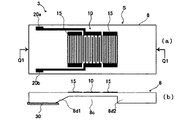
図1は、本発明の一実施形態としての力検知ユニットの構成例を示す図であり、同図(a)は平面図、同図(b)、同図(c)は夫々Q1−Q1、及びQ2−Q2における断面図である。本発明に係る力検知ユニット1は、平行な2本の細幅帯状の圧電片8a、8bを連結支持部9によりコ字状に一体化した圧電基板8と、2本の圧電片8a、8bの各一方の主面(上面)から連結支持部9にかけて夫々形成された送信用及び受信用の各IDT電極10、11及び12、13(以下、送受一対のIDT電極、という)と、を有した力感応素子Sと、力感応素子Sの連結支持部9の他方の主面(下面)を接着保持する支持基板Pと、を備えた力検知ユニット1である。そして、一方の圧電片8aに形成した送受一対のIDT電極10、11と、他方の圧電片8bに形成した送受一対のIDT電極12、13と、を夫々並列接続する。更に、他方の圧電片8bに形成した送受一対のIDT電極12、13のうち、受信側のIDT電極13を反転接続して構成する。また、6個のボンディングパッド20a〜20fは連結支持部9の左側に形成し、その外側と、圧電片8a、8bの右側端部とには夫々音波吸収材25を塗布する。
Hereinafter, embodiments of the present invention will be described in detail with reference to the drawings.
FIG. 1 is a diagram illustrating a configuration example of a force detection unit according to an embodiment of the present invention, in which FIG. 1A is a plan view, FIG. 1B and FIG. 1C are Q1-Q1, respectively. And is a cross-sectional view at Q2-Q2. The force detection unit 1 according to the present invention includes a piezoelectric substrate 8 in which two parallel narrow strips of piezoelectric pieces 8a and 8b are integrated in a U shape by a connection support portion 9, and two piezoelectric pieces 8a and 8b. Transmitting and receiving IDT electrodes 10, 11 and 12, 13 (hereinafter referred to as a pair of transmitting and receiving IDT electrodes) respectively formed from one main surface (upper surface) to the connection support portion 9. The force detection unit 1 includes the force-sensitive element S and the support substrate P that adheres and holds the other main surface (lower surface) of the connection support portion 9 of the force-sensitive element S. The pair of transmission / reception IDT electrodes 10 and 11 formed on one piezoelectric piece 8a and the pair of transmission / reception IDT electrodes 12 and 13 formed on the other piezoelectric piece 8b are connected in parallel. Further, among the pair of IDT electrodes 12 and 13 formed on the other piezoelectric piece 8b, the IDT electrode 13 on the receiving side is reversely connected. The six bonding pads 20a to 20f are formed on the left side of the connection support portion 9, and the sound absorbing material 25 is applied to the outside and the right end portions of the piezoelectric pieces 8a and 8b, respectively.

図1(a)に示すように、IDT電極10の上のバスバーをボンディングパッド20aに、IDT電極10の下のバスバーと、IDT電極11の上のバスバーとをボンディングパッド20bに、IDT電極11の下のバスバーをボンディングパッド20cに、夫々接続する。更に、IDT電極12の上のバスバーをボンディングパッド20dに、IDT電極12の下のバスバーと、IDT電極13の上のバスバーとをボンディングパッド20eに、IDT電極13の下のバスバーをボンディングパッド20fに、夫々接続する。そして、ボンディングパッド20aと20dを接続し、ボンディングパッド20bと20eを接続して入力側のIDT電極10、12を並列接続する。同様に、ボンディングパッド20cと20fを接続し、出力側のIDT電極11、13を並列接続して、本発明に係る力検知ユニット1を構成する。なお、ボンディングパッド20bと20eは接地する。IDT電極10〜13は、互いに間挿し合う複数の電極指からなり、その電極材料はアルミニウム合金等を用いる。IDT電極10〜12における電極指のバスバーへの接続と、IDT電極13における電極指のバスバーへの接続とは異なるように形成する。IDT電極10とIDT電極12の極性が互いに同相に、且つIDT電極11とIDT電極13の極性が互いに逆相となるように接続する。   As shown in FIG. 1A, the bus bar above the IDT electrode 10 is used as the bonding pad 20a, the bus bar below the IDT electrode 10 and the bus bar above the IDT electrode 11 are used as the bonding pad 20b, and the IDT electrode 11 The lower bus bars are connected to the bonding pads 20c, respectively. Further, the bus bar above IDT electrode 12 is used as bonding pad 20d, the bus bar below IDT electrode 12 and the bus bar above IDT electrode 13 are used as bonding pad 20e, and the bus bar below IDT electrode 13 is used as bonding pad 20f. , Connect each one. Then, the bonding pads 20a and 20d are connected, the bonding pads 20b and 20e are connected, and the input-side IDT electrodes 10 and 12 are connected in parallel. Similarly, the bonding pads 20c and 20f are connected, and the IDT electrodes 11 and 13 on the output side are connected in parallel to constitute the force detection unit 1 according to the present invention. The bonding pads 20b and 20e are grounded. The IDT electrodes 10 to 13 are composed of a plurality of electrode fingers interleaved with each other, and an aluminum alloy or the like is used as the electrode material. The connection between the electrode fingers of the IDT electrodes 10 to 12 and the bus bar is different from the connection of the electrode fingers of the IDT electrode 13 to the bus bar. The IDT electrode 10 and the IDT electrode 12 are connected so that their polarities are in phase with each other, and the IDT electrode 11 and the IDT electrode 13 are in reverse phases with each other.

図1(b)、(c)に示すように、一方の圧電片8a及び連結支持部9は、均一厚の厚肉部であり、他方の圧電片8bは、前記厚肉部よりも薄い薄肉部を有するように、圧電基板8を構成する。図1(b)に示すように、トラックT1を構成する連結支持部9と圧電片8aとの厚さは、圧電片8aに垂直方向から外力が加えられた場合にも撓まないような厚さとする。一方、トラックT2を構成する連結支持部9と圧電片8bの厚さは、連結支持部9と圧電片8bとの境界近傍で漸減し、圧電片8bの薄肉部は一様の厚さに形成されている。圧電片8bに垂直方向から外力が加えられた場合には圧電片8bが撓むように構成されている。図1(a)に示した実施例では、各圧電片8a、8bに送受一対のIDT電極を形成した例を示したが、送受二対、送受三対のIDT電極を設けてもよい。   As shown in FIGS. 1B and 1C, one piezoelectric piece 8a and the connecting support portion 9 are thick portions having a uniform thickness, and the other piezoelectric piece 8b is a thin wall portion thinner than the thick portion. The piezoelectric substrate 8 is configured to have a portion. As shown in FIG. 1B, the thickness of the connection support portion 9 and the piezoelectric piece 8a constituting the track T1 is such that the piezoelectric piece 8a does not bend even when an external force is applied from the vertical direction. Say it. On the other hand, the thickness of the connecting support portion 9 and the piezoelectric piece 8b constituting the track T2 gradually decreases in the vicinity of the boundary between the connecting support portion 9 and the piezoelectric piece 8b, and the thin portion of the piezoelectric piece 8b is formed to have a uniform thickness. Has been. The piezoelectric piece 8b is configured to bend when an external force is applied to the piezoelectric piece 8b from the vertical direction. In the embodiment shown in FIG. 1A, an example in which a pair of transmission / reception IDT electrodes is formed on each piezoelectric piece 8a, 8b is shown, but two pairs of transmission / reception IDTs and three pairs of transmission / reception IDT electrodes may be provided.

図2は、支持基板Pとしてセラミックパッケージを用いた例で、力検知ユニット素子Sの連結支持部9の裏面側を、セラミックパッケージの凹陥部の内底面に接着剤30を用いて接着固定し、力検知ユニット素子Sのボンディングパッドと、セラミックパッケージの周縁に形成した電極部とを、ボンディングワイヤ35にて接続して力検知ユニット1を構成した例である。なお、図2に示した力検知ユニット1は、力検知ユニット素子1とセラミックパッケージPの電極部とのボンディング回数を少なくするため、リード電極の配線とボンディングパッドの位置とに工夫を施した例である。   FIG. 2 is an example in which a ceramic package is used as the support substrate P, and the back surface side of the connection support portion 9 of the force detection unit element S is bonded and fixed to the inner bottom surface of the recessed portion of the ceramic package using an adhesive 30. In this example, the force detection unit 1 is configured by connecting the bonding pads of the force detection unit element S and the electrode portions formed on the periphery of the ceramic package with bonding wires 35. The force detection unit 1 shown in FIG. 2 is an example in which the wiring of the lead electrode and the position of the bonding pad are devised in order to reduce the number of times of bonding between the force detection unit element 1 and the electrode portion of the ceramic package P. It is.

図3、図4は、本発明の動作を説明するためのIDT電極の概略図であって、図3は力検知ユニットに外力が加わっていない状態(外力無印加時)を、図4は外力Fが加わった状態(外力印加時)を示している。IDT電極10、12を並列接続して入力側とし、IDT電極11、13を並列接続して出力側とする。入力側のIDT電極10、12に高周波電圧を加えて弾性表面波を励起し、該弾性表面波がトラックT1、T2上を伝搬し、出力側のIDT電極11、13に到達して、IDT電極11、13上に電荷が発生する。図3はある瞬間の電荷の発生状態を示したものである。IDT電極13の電極指とバスバーとの接続が、他のIDT電極10〜12と異なる、つまり反転しているため、IDT電極11、13を並列接続すると、IDT電極11、13上に発生した電荷は互いに打ち消し合い、出力OUTの電圧はほぼ零となる。   3 and 4 are schematic diagrams of IDT electrodes for explaining the operation of the present invention. FIG. 3 shows a state in which no external force is applied to the force detection unit (when no external force is applied), and FIG. A state where F is applied (when an external force is applied) is shown. The IDT electrodes 10 and 12 are connected in parallel to be an input side, and the IDT electrodes 11 and 13 are connected in parallel to be an output side. A high frequency voltage is applied to the IDT electrodes 10 and 12 on the input side to excite surface acoustic waves, the surface acoustic waves propagate on the tracks T1 and T2, reach the IDT electrodes 11 and 13 on the output side, and then IDT electrodes Charges are generated on 11 and 13. FIG. 3 shows the state of charge generation at a certain moment. Since the connection between the electrode finger of the IDT electrode 13 and the bus bar is different from the other IDT electrodes 10 to 12, that is, is inverted, the charge generated on the IDT electrodes 11 and 13 when the IDT electrodes 11 and 13 are connected in parallel. Cancel each other, and the voltage at the output OUT becomes almost zero.

一方、入力側IDT電極10、12に高周波電圧を加えて弾性表面波を励起した状態で、図4(a)に示すように力検知ユニットに外力Fが印加された場合を考える。トラックT1を構成する連結支持部9と圧電片8aとは、肉厚に形成されているため、外力Fが印加された場合にも撓まず、圧電片8aに歪みは生じない。しかるに、トラックT2を構成する連結支持部9と圧電片8bとは、連結支持部9と圧電片8bとの境界近傍で厚さが漸減し、圧電片8bは一様な薄肉に形成されている。このため外力Fが圧電片8bに印加されると、圧電片8bは撓み、圧電片8b全体に歪みが生じる。歪みが生じている状態では、弾性表面波の伝搬速度が変化し、図4(b)に示すように、ある瞬間にIDT電極13に発生する電荷は、同時刻にIDT電極11に発生する電荷と異なる。その結果、IDT電極11、13を並列接続した出力OUTには、IDT電極11、13の夫々に発生した電荷の差が発生することになる。IDT電極13に発生する電荷は印加する外力に応じて変化するので、出力OUTの電荷(電圧)により印加された力の大きさが分かる。   On the other hand, consider a case where an external force F is applied to the force detection unit as shown in FIG. 4A in a state where a high frequency voltage is applied to the input-side IDT electrodes 10 and 12 to excite a surface acoustic wave. Since the connecting support portion 9 and the piezoelectric piece 8a constituting the track T1 are formed thick, even when an external force F is applied, the piezoelectric piece 8a does not bend and the piezoelectric piece 8a is not distorted. However, the thickness of the connecting support portion 9 and the piezoelectric piece 8b constituting the track T2 gradually decreases in the vicinity of the boundary between the connecting support portion 9 and the piezoelectric piece 8b, and the piezoelectric piece 8b is formed in a uniform thin wall. . For this reason, when the external force F is applied to the piezoelectric piece 8b, the piezoelectric piece 8b bends and the entire piezoelectric piece 8b is distorted. In the state where distortion occurs, the propagation speed of the surface acoustic wave changes, and as shown in FIG. 4B, the charge generated in the IDT electrode 13 at a certain moment is the charge generated in the IDT electrode 11 at the same time. And different. As a result, a difference in charge generated in each of the IDT electrodes 11 and 13 occurs in the output OUT in which the IDT electrodes 11 and 13 are connected in parallel. Since the charge generated in the IDT electrode 13 changes according to the applied external force, the magnitude of the force applied by the charge (voltage) of the output OUT can be known.

図5は、本発明に係る力検知ユニットとしての第2の実施例を示す図であり、IDT電極10〜13とその接続状態のみを示す図である。圧電片8a、8b、連結支持部9からなる圧電基板8と、リード電極と、ボンディングパッド20a〜20fと、音波吸収材25と、は図示しないが、図1と同様に構成されている。ただ、図1と異なる点は、図5に示す第2の実施例では、圧電片8a、8bに形成した送受一対のIDT電極10〜13の中、受信側のIDT電極11の極性を反転し、IDT電極13では、左から奇数番目の電極指を接地して構成している。これに対し、図1のIDT電極13では左から偶数番目が接地されている。要するに、夫々送受一対のIDT電極10、11とIDT電極12、13との間で、位相差が互いに180°異なるように構成されている。図1と同様に、IDT電極10、12を並列接続して入力側INとし、IDT電極11、13を並列接続して出力側OUTとする。図5に示すIDT電極構成で、入力IN側のIDT電極10、12に高周波電圧を加えて弾性表面波を励起し、該弾性表面波がトラックT1、T2上を伝搬し、出力側のIDT電極11、13に到達して、IDT電極11、13に電荷が発生する。IDT電極11とIDT電極13とは極性を反転しているため、IDT電極11、13を並列することにより、IDT電極11、13上に発生した電荷は互いに打ち消し合い、出力OUT側の電荷(電圧)はほぼ零となる。図5の力検知ユニットに力外Fが印加されると、トラックT1は歪まないので弾性表面波の伝搬速度に変化はないが、トラックT2は外力Fによる歪みのために、弾性表面波の伝搬速度が変化し、出力OUTに電荷(電圧)が発生する。この電圧により印加された力の大きさを測定する。 FIG. 5 is a diagram showing a second embodiment as a force detection unit according to the present invention, and shows only the IDT electrodes 10 to 13 and their connection states. The piezoelectric substrate 8 including the piezoelectric pieces 8a and 8b and the connection support portion 9, the lead electrode, the bonding pads 20a to 20f, and the sound absorbing material 25 are not illustrated, but are configured in the same manner as in FIG. However, the difference from FIG. 1 is that in the second embodiment shown in FIG. 5, the polarity of the IDT electrode 11 on the receiving side of the pair of IDT electrodes 10 to 13 formed on the piezoelectric pieces 8a and 8b is reversed. The IDT electrode 13 is configured by grounding odd-numbered electrode fingers from the left. On the other hand, even numbers from the left are grounded in the IDT electrode 13 of FIG. In short, the phase difference between the pair of transmission / reception IDT electrodes 10 and 11 and the IDT electrodes 12 and 13 is different from each other by 180 ° . As in FIG. 1, the IDT electrodes 10 and 12 are connected in parallel to be an input side IN, and the IDT electrodes 11 and 13 are connected in parallel to be an output side OUT. In the IDT electrode configuration shown in FIG. 5, a high frequency voltage is applied to the IDT electrodes 10 and 12 on the input IN side to excite surface acoustic waves, and the surface acoustic waves propagate on the tracks T1 and T2, and the IDT electrodes on the output side 11 and 13, and charges are generated in the IDT electrodes 11 and 13. Since the IDT electrode 11 and the IDT electrode 13 are reversed in polarity, the charges generated on the IDT electrodes 11 and 13 cancel each other out by arranging the IDT electrodes 11 and 13 in parallel, and the charges on the output OUT side (voltage ) Is almost zero. When the external force F is applied to the force detection unit of FIG. 5, the track T1 is not distorted and the propagation speed of the surface acoustic wave is not changed, but the track T2 is propagated by the surface acoustic wave due to the distortion caused by the external force F. The speed changes and a charge (voltage) is generated at the output OUT. The magnitude of the force applied by this voltage is measured.

図6(a)は、図1に示した力検知ユニット1に外力Fを加えない状態で、入力側に高周波電圧を印加した場合、出力側に発生した電圧波形を示した図である。出力電圧は、IDT電極間の長さの精度、IDT電極を構成する電極指の精度等により、完全には零とならないが、極めて小さい。一方、図6(b)は、入力側に高周波電圧を印加した状態で、外力Fを加えた場合の出力側に発生する電圧波形を示した図である。   FIG. 6A is a diagram showing a voltage waveform generated on the output side when a high frequency voltage is applied to the input side in the state where the external force F is not applied to the force detection unit 1 shown in FIG. The output voltage is not completely zero due to the accuracy of the length between the IDT electrodes, the accuracy of the electrode fingers constituting the IDT electrode, and the like, but is extremely small. On the other hand, FIG. 6B is a diagram showing a voltage waveform generated on the output side when an external force F is applied with a high frequency voltage applied to the input side.

図7は、力検知ユニットの出力側に発生する電圧から印加された外力Fの大きさを求める処理方法の一例を示した図である。力検知ユニットの入力側に(a)の高周波電圧信号が入力されると、出力側から外力に応じて(b)の出力電圧が得られる。この出力電圧を全波整流すると(c)の波形の電圧が得られる。この電圧を(d)の積分回路に入力すると、(e)に示す直流電圧が得られる。この直流電圧の大きさから印加された外力Fの大きさを求める。   FIG. 7 is a diagram illustrating an example of a processing method for obtaining the magnitude of the external force F applied from the voltage generated on the output side of the force detection unit. When the high-frequency voltage signal (a) is input to the input side of the force detection unit, the output voltage (b) is obtained from the output side according to the external force. When this output voltage is full-wave rectified, a voltage having the waveform (c) is obtained. When this voltage is input to the integration circuit of (d), a DC voltage shown in (e) is obtained. The magnitude of the applied external force F is determined from the magnitude of the DC voltage.

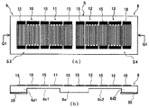
図8は、力検知ユニットに係る第3の実施例の構成を示す図であり、同図(a)は平面図、同図(b)、(c)は夫々Q1−Q1、Q2−Q2における断面図である。第3の実施例の力検知ユニットは、図8(a)に示すように、IDT電極10〜13と、リード電極と、ボンディングパッドとは、図1に示した第1の実施例と同様である。しかし、圧電基板8は、図8(b)、(c)に示すように、一方の圧電片8a及び連結支持部9は、均一厚の厚肉部であり、他方の圧電片8bは、その一方の主面の略中央部に凹陥部8cを形成することにより形成した薄肉部を有すると共に両端部に厚肉部(連結支持部9と厚肉部8d)を有している。第3の実施例の力検知ユニットの特徴は、図1に示した第1の実施例の力検知ユニットに比べ、圧電片8bの端部に厚肉部8dを設けているので、力検知ユニットの感度を高めることができる。例えば、この力検知ユニットを加速度検知ユニットとして用いると、加速度×質量が力となり、質量が大きい程、検出感度を高められるからである。図8に示した第3の実施例の場合も、各振動片8a、8bに形成するIDT電極の対数は少なくとも1対とする。   FIG. 8 is a diagram showing a configuration of a third embodiment according to the force detection unit. FIG. 8A is a plan view, and FIGS. 8B and 8C are views in Q1-Q1 and Q2-Q2, respectively. It is sectional drawing. As shown in FIG. 8A, the force detection unit of the third embodiment has the same IDT electrodes 10 to 13, lead electrodes, and bonding pads as those of the first embodiment shown in FIG. is there. However, as shown in FIGS. 8B and 8C, in the piezoelectric substrate 8, one piezoelectric piece 8a and the connecting support portion 9 are thick portions having a uniform thickness, and the other piezoelectric piece 8b is One main surface has a thin portion formed by forming a recessed portion 8c at a substantially central portion, and has thick portions (connection support portion 9 and thick portion 8d) at both ends. The feature of the force detection unit of the third embodiment is that the thick portion 8d is provided at the end of the piezoelectric piece 8b as compared with the force detection unit of the first embodiment shown in FIG. Can increase the sensitivity. For example, when this force detection unit is used as an acceleration detection unit, acceleration × mass becomes force, and the detection sensitivity increases as the mass increases. Also in the case of the third embodiment shown in FIG. 8, at least one pair of IDT electrodes is formed on each of the resonator elements 8a and 8b.

図9は、力検知ユニットに係る第4の実施例の構成を示す図であり、同図(a)は平面図、同図(b)はQ1−Q1における断面図である。第4の実施例の力検知ユニット2は、一方の主面の略中央部に凹陥部8cを形成することにより形成した薄肉部を有すると共に両端部に厚肉部8d1、8d2を有した圧電基板8と、圧電基板8の他方の主面上の両端部寄りに夫々一個ずつ形成したIDT電極10、11と、を有した力感応素子Sと、力感応素子Sの一方の厚肉部8d1の一方の主面側を接着剤30により接着保持する支持基板Pと、を備えた力検知ユニット2である。接着剤30の厚みを利用して圧電基板8の他方の厚肉部8d2を支持基板P上から離間させた片持ち支持とした力検知ユニットを構成する。   FIGS. 9A and 9B are diagrams showing the configuration of the fourth embodiment according to the force detection unit, where FIG. 9A is a plan view and FIG. 9B is a cross-sectional view taken along Q1-Q1. The force detection unit 2 according to the fourth embodiment has a thin portion formed by forming a recessed portion 8c at a substantially central portion of one main surface, and has a thick portion 8d1, 8d2 at both ends. 8 and IDT electrodes 10 and 11 formed one by one near both ends on the other main surface of the piezoelectric substrate 8, and one thick portion 8d1 of the force sensitive element S This is a force detection unit 2 including a support substrate P on which one main surface side is bonded and held by an adhesive 30. By using the thickness of the adhesive 30, a force detection unit is configured in which the other thick part 8 d 2 of the piezoelectric substrate 8 is cantilevered and separated from the support substrate P.

図9(a)に示すように、略中央部に凹陥部8cを形成した細幅帯状の圧電基板8の両端部寄りであって、厚肉部8d1、8d2と対向する主面にIDT電極10、11を夫々形成する。厚肉部8d1の端にボンディングパッド20a、20b、20cを形成し、その外側と、厚肉部8d2の端部とに音波吸収材25を塗布する。IDT電極10の上のバスバーと、ボンディングパッド20aとをリード電極にて接続し、IDT電極10の下のバスバー及びIDT電極11の上のバスバーをリード電極にてボンディングパッド20bと接続する。IDT電極11の下のバスバーと、ボンディングパッド20cとをリード電極にて接続し、ボンディングパッド20a、20b、20cは支持基板Pの電極部Tにボンディングワイヤで夫々接続して力検知ユニット2を構成する。なお、図9(a)に示した第4の実施例の場合も、圧電基板8に形成するIDT電極の対数は少なくとも1対とする。   As shown in FIG. 9 (a), the IDT electrode 10 is formed on the main surface near the both end portions of the narrow band-shaped piezoelectric substrate 8 having the recessed portion 8c formed in the substantially central portion and opposed to the thick portions 8d1 and 8d2. , 11 are formed. Bonding pads 20a, 20b and 20c are formed at the end of the thick part 8d1, and the sound absorbing material 25 is applied to the outside and the end of the thick part 8d2. The bus bar on the IDT electrode 10 and the bonding pad 20a are connected by a lead electrode, and the bus bar on the IDT electrode 10 and the bus bar on the IDT electrode 11 are connected to the bonding pad 20b by a lead electrode. The bus bar under the IDT electrode 11 and the bonding pad 20c are connected by a lead electrode, and the bonding pads 20a, 20b and 20c are respectively connected to the electrode portion T of the support substrate P by a bonding wire to constitute the force detection unit 2. To do. In the case of the fourth embodiment shown in FIG. 9A, the number of IDT electrodes formed on the piezoelectric substrate 8 is at least one pair.

IDT電極10と11とで遅延型の弾性表面波共振子を構成し、IDT電極10、11の波長λで決まる共振周波数f0を有する。IDT電極10に高周波電圧を印加すると、IDT電極11から共振周波数f0の応答が得られる。いま、圧電基板8の厚肉部8d2に外力Fが加わると凹陥部8cの薄肉部が撓んで、薄肉部に歪みが生じる。IDT電極10に高周波電圧を印加した状態で、厚肉部8d2に外力Fを加えると、外力Fに応じた歪みが生じ、前記薄肉部を伝搬する弾性表面波の速度が変化する。その結果、IDT電極11でピックアップする周波数が変化することになる。図10は、図9に示す力検知ユニット2の入力IDT電極10に高周波電圧を印加し、出力IDT電極11でピックアップした場合の周波数応答を示す図で、実線は力検知ユニット2に外力を加えない場合(力無印加時)の周波数応答(通常応答)を示した図である。破線は、力検知ユニット2に力を加えた場合(力印加時)の周波数応答(応力印加応答)を示した図である。力検知ユニット2に力を加えた場合は、弾性表面波の伝搬路である薄肉部に歪みが生じているために、弾性表面波の伝搬速度が変化し、共振周波数が低周波側にシフトする。周波数のシフトは印加する力Fに応じて変化する。従って、周波数のシフト量を測定することにより、印加された力Fの大きさを計ることできる。   The IDT electrodes 10 and 11 constitute a delay type surface acoustic wave resonator, and have a resonance frequency f 0 determined by the wavelength λ of the IDT electrodes 10 and 11. When a high frequency voltage is applied to the IDT electrode 10, a response having a resonance frequency f 0 is obtained from the IDT electrode 11. Now, when an external force F is applied to the thick part 8d2 of the piezoelectric substrate 8, the thin part of the recessed part 8c bends and distortion occurs in the thin part. When an external force F is applied to the thick portion 8d2 in a state where a high frequency voltage is applied to the IDT electrode 10, distortion corresponding to the external force F occurs, and the velocity of the surface acoustic wave propagating through the thin portion changes. As a result, the frequency picked up by the IDT electrode 11 changes. FIG. 10 is a diagram showing a frequency response when a high frequency voltage is applied to the input IDT electrode 10 of the force detection unit 2 shown in FIG. 9 and picked up by the output IDT electrode 11, and the solid line indicates an external force applied to the force detection unit 2. It is the figure which showed the frequency response (normal response) when there is no (when no force is applied). A broken line is a diagram showing a frequency response (stress application response) when a force is applied to the force detection unit 2 (when a force is applied). When a force is applied to the force detection unit 2, since the thin wall portion that is the propagation path of the surface acoustic wave is distorted, the propagation speed of the surface acoustic wave changes and the resonance frequency shifts to the low frequency side. . The frequency shift changes according to the applied force F. Therefore, the magnitude of the applied force F can be measured by measuring the frequency shift amount.

図11は、力検知ユニットに係る第5の実施例の構成を示す図であり、同図(a)は平面図、同図(b)はQ1−Q1における断面図である。第5の実施例の力検知ユニット2は、一方の主面の略中央部に凹陥部8cを形成することにより形成した薄肉部を有すると共に、両端部に厚肉部8d1、8d2を有した圧電基板8と、該圧電基板8の他方の主面上の両端部寄りに夫々一個ずつ形成したIDT電極10、11と、を有した力感応素子Sと、該力感応素子Sの一方の厚肉部8d1の一方の主面側を接着保持する支持基板Pと、を備えた力検知ユニットである。そして、支持基板Pの所定の位置に接着剤30を塗布し、その上に所定の厚みを有した接合材33を乗せ、その上に接着剤30を塗布し、これに圧電基板8の一方の厚肉部8d1を載置して圧電基板8を接着保持し、且つ他方の厚肉部8d2を支持基板Pの面から離間させた片持ち支持とした力検知ユニット2を構成する。または、支持基板P面に設けた突部(図示せず)に接着剤30を塗布し、これに圧電基板8の一方の厚肉部8d1を載置して、圧電基板8を接着保持し、且つ他方の厚肉部8d2を支持基板Pの面から離間させた片持ち支持とした力検知ユニット2を構成する。なお、図11(a)に示した第5の実施例の場合も、圧電基板8に形成するIDT電極の対数は少なくとも1対とする。   FIG. 11 is a diagram showing a configuration of a fifth embodiment according to the force detection unit, where FIG. 11A is a plan view and FIG. 11B is a cross-sectional view taken along Q1-Q1. The force detection unit 2 of the fifth embodiment has a thin portion formed by forming a recessed portion 8c at a substantially central portion of one main surface, and has a thick portion 8d1, 8d2 at both ends. A force-sensitive element S having a substrate 8 and IDT electrodes 10 and 11 formed one by one near both ends of the other main surface of the piezoelectric substrate 8, and one thick wall of the force-sensitive element S And a support substrate P that adheres and holds one main surface side of the portion 8d1. Then, the adhesive 30 is applied to a predetermined position of the support substrate P, the bonding material 33 having a predetermined thickness is placed thereon, the adhesive 30 is applied thereon, and one of the piezoelectric substrates 8 is applied thereto. The force detection unit 2 is configured such that the thick portion 8d1 is placed and the piezoelectric substrate 8 is adhered and held, and the other thick portion 8d2 is cantilevered away from the surface of the support substrate P. Alternatively, an adhesive 30 is applied to a protrusion (not shown) provided on the surface of the support substrate P, and one thick portion 8d1 of the piezoelectric substrate 8 is placed on the protrusion 30 to adhere and hold the piezoelectric substrate 8. In addition, the force detection unit 2 is configured in which the other thick portion 8d2 is cantilevered and separated from the surface of the support substrate P. In the case of the fifth embodiment shown in FIG. 11A, the number of IDT electrodes formed on the piezoelectric substrate 8 is at least one pair.

図11に示す第5の実施例の構成が、図9に示した第4の実施例の構成と異なる点は、支持基板Pと接着剤30との間に、接着剤30を塗布した適当な厚みの接合材33とを挟んで、支持基板Pの面と、圧電基板8の厚肉部8d2との間の隙間を広げた点である(図9では接着剤の厚みにより片持ち支持としている)。又は、接合材33の代わりに所定の厚みの突部(図示せず)を支持基板Pに予め形成しておいてもよい。このように接合材33、又は突部のある支持基板Pを用いて、第5の実施例の力検知ユニットを構成にすれば、接着剤30の厚みにバラツキが生じた場合、圧電基板8に外力Fが加わり、凹陥部8cの薄肉部に撓みが生じても、厚肉部8d2が支持基板Pの面と接着し、測定誤差を来すことはない。
また、接合材33の具体例としては、半田バンプやAuバンプなどがある。支持基板がアルカリ金属イオンを含むガラスである場合は、力感応素子の支持基板側にAl膜などを設けることにより力感応素子と支持基板を陽極接合することも可能である。
The configuration of the fifth embodiment shown in FIG. 11 is different from the configuration of the fourth embodiment shown in FIG. 9 in that an adhesive 30 is applied between the support substrate P and the adhesive 30. The gap between the surface of the support substrate P and the thick portion 8d2 of the piezoelectric substrate 8 is widened across the bonding material 33 having a thickness (in FIG. 9, the cantilever is supported by the thickness of the adhesive). ). Alternatively, a protrusion (not shown) having a predetermined thickness may be formed in advance on the support substrate P instead of the bonding material 33. If the force detection unit of the fifth embodiment is configured using the bonding material 33 or the support substrate P having the protrusions in this way, when the thickness of the adhesive 30 varies, the piezoelectric substrate 8 Even if the external force F is applied and the thin portion of the recessed portion 8c is bent, the thick portion 8d2 adheres to the surface of the support substrate P and does not cause a measurement error.
Specific examples of the bonding material 33 include solder bumps and Au bumps. When the support substrate is glass containing alkali metal ions, the force sensitive element and the support substrate can be anodically bonded by providing an Al film or the like on the support substrate side of the force sensitive element.

図12は、力検知ユニットに係る第6の実施例の構成を示す断面図である。第6の実施例の力検知ユニットが第4の実施例と異なる点は、第4の実施例の圧電基板8の厚肉部8d2の上に他の圧電基板、あるいは他のチップ部品を接着固定した点である。チップ部品には発振回路部品等も含まれる。支持基板P上に一方の厚肉部8d1を接着保持される圧電基板8の他方の厚肉部8d2の他方の主面上に重りとして、他の圧電基板7、或いは発振回路部品(その他の回路部品)を接着して力検知ユニットを構成する。このように構成した力検知ユニットを、例えば加速度センサに用いれば、圧電基板7、又は発振回路部品の重さにより、加速度センサの感度が向上するという効果がある。   FIG. 12 is a cross-sectional view showing the configuration of the sixth embodiment according to the force detection unit. The force detection unit of the sixth embodiment is different from the fourth embodiment in that another piezoelectric substrate or another chip component is bonded and fixed on the thick portion 8d2 of the piezoelectric substrate 8 of the fourth embodiment. This is the point. Chip components include oscillator circuit components and the like. As a weight on the other main surface of the other thick part 8d2 of the piezoelectric substrate 8 to which one thick part 8d1 is bonded and held on the support substrate P, another piezoelectric substrate 7 or an oscillation circuit component (other circuit) The force detection unit is configured by bonding components. If the force detection unit configured in this way is used for an acceleration sensor, for example, the sensitivity of the acceleration sensor is improved by the weight of the piezoelectric substrate 7 or the oscillation circuit component.

図13は、力検知ユニットに係る第7の実施例の構成を示す断面図である。第7の実施例の力検知ユニット2が第4の実施例と異なる点は、第4の実施例の圧電基板8の厚肉部8d2の上に金属フィラー接着剤41を塗布して設けた点である。つまり、支持基板P上に一方の厚肉部8d1を接着保持される圧電基板8の他方の厚肉部8d2の一方の主面、又は/及び、他方の主面に重りとしての金属フィラー接着剤41を配置した力検知ユニットを構成する。このように構成した力検知ユニットを、例えば加速度センサに用いれば、金属フィラー接着剤41の重さにより、加速度センサの感度が向上するという効果ある。   FIG. 13 is a cross-sectional view showing a configuration of a seventh embodiment according to the force detection unit. The difference between the force detection unit 2 of the seventh embodiment and the fourth embodiment is that a metal filler adhesive 41 is applied on the thick portion 8d2 of the piezoelectric substrate 8 of the fourth embodiment. It is. That is, the metal filler adhesive as a weight on one main surface and / or the other main surface of the other thick portion 8d2 of the piezoelectric substrate 8 on which the one thick portion 8d1 is bonded and held on the support substrate P. The force detection unit 41 is configured. If the force detection unit configured in this way is used for, for example, an acceleration sensor, the sensitivity of the acceleration sensor is improved by the weight of the metal filler adhesive 41.

図14は、力検知ユニットに係る第8の実施例の構成を示す図で、同図(a)は平面図、同図(b)はQ1−Q1における断面図である。第8の実施例の力検知ユニット3は、一方の主面の略中央部に凹陥部8cを形成することにより形成した薄肉部を有すると共に両端部に厚肉部8d1、8d2を有した圧電基板8、該圧電基板8の他方の主面上に形成されたIDT電極8及びグレーティング反射器(以下、反射器と称す)15を有した力感応素子Sと、該力感応素子Sの一方の厚肉部8d1の一方の主面側を接着保持する支持基板Pと、を備えた力検知ユニットである。そして、IDT電極8を前記薄肉部上に配置し、2個の反射器15、15を両厚肉部8d1、8d2上に夫々配置する。また、ボンディングパッド20a、20bは圧電基板8の厚肉部の隅部に形成する。IDT電極10の上のバスバーをリード電極にてボンディングパッド20aに接続し、下のバスバーをリード電極にてボンディングパッド20bに接続して力検知ユニット3を構成する。   14A and 14B are diagrams showing the configuration of the eighth embodiment according to the force detection unit, where FIG. 14A is a plan view and FIG. 14B is a cross-sectional view taken along Q1-Q1. The force detection unit 3 of the eighth embodiment has a thin-walled portion formed by forming a recessed portion 8c in a substantially central portion of one main surface, and has a thick-walled portion 8d1, 8d2 at both ends. 8, a force sensitive element S having an IDT electrode 8 and a grating reflector (hereinafter referred to as a reflector) 15 formed on the other main surface of the piezoelectric substrate 8, and one thickness of the force sensitive element S And a support substrate P that adheres and holds one main surface side of the meat portion 8d1. The IDT electrode 8 is disposed on the thin portion, and the two reflectors 15 and 15 are disposed on the thick portions 8d1 and 8d2, respectively. The bonding pads 20 a and 20 b are formed at the corners of the thick portion of the piezoelectric substrate 8. The force detection unit 3 is configured by connecting the bus bar above the IDT electrode 10 to the bonding pad 20a with a lead electrode and connecting the lower bus bar to the bonding pad 20b with a lead electrode.

図14に示す力検知ユニット3は、IDT電極10と、その両側に配置した2個の反射器15、15と、で弾性表面波共振子(SAW共振子)を構成し、その共振周波数f0はIDT電極10の波長λで決まる。ボンディングパッド20a、20bに発振回路を接続すると、発振回路の出力端子から周波数f0が得られる。発振させた状態で、圧電基板8に外力Fを印加すると、圧電基板8の前記薄肉部に歪みが生じ、この歪みにより圧電基板8の表面を伝搬する弾性表面波の伝搬速度が変化する。伝搬速度が変化することにより、SAW共振子の共振周波数f0がf’0に変化し、発振回路からの出力周波数はf’0になる。周波数変化量(f0−f’0)は、印加する力に応じて変化する。周波数変化量(f0−f’0)から加わった外力Fの大きさを知ることがきる。   In the force detection unit 3 shown in FIG. 14, a surface acoustic wave resonator (SAW resonator) is constituted by the IDT electrode 10 and the two reflectors 15 and 15 arranged on both sides thereof, and the resonance frequency f0 is It is determined by the wavelength λ of the IDT electrode 10. When an oscillation circuit is connected to the bonding pads 20a and 20b, the frequency f0 is obtained from the output terminal of the oscillation circuit. When an external force F is applied to the piezoelectric substrate 8 in the oscillated state, the thin portion of the piezoelectric substrate 8 is distorted, and the propagation speed of the surface acoustic wave propagating on the surface of the piezoelectric substrate 8 changes due to the distortion. As the propagation speed changes, the resonance frequency f0 of the SAW resonator changes to f'0, and the output frequency from the oscillation circuit becomes f'0. The frequency change amount (f0−f′0) changes according to the applied force. It is possible to know the magnitude of the external force F applied from the frequency change amount (f0−f′0).

図15は、力検知ユニットに係る第9の実施例の構成を示す図で、同図(a)は平面図、同図(b)はQ1−Q1における断面図である。第9の実施例の力検知ユニットは、支持基板P上に一方の厚肉部8d1を接着保持される圧電基板8の他方の厚肉部8d2の一方の主面、又は/及び、他方の主面に重りとしての金属膜40を蒸着するか、又は金属部材40を接着した力検知ユニットを構成する。圧電基板8、IDT電極10、グレーティング反射器15、リード電極、ボンディングパッド20a、20bは、図14に示した第8の実施例と同様に構成する。つまり、第9の実施例の力検知ユニットが、第8の実施例の力検知ユニットと異なる点は、圧電基板8の厚肉部8d2の上、又は下、あるいは上下に重りとなる金属膜40、又は金属部材40を接着した点である。図16は、第9の実施例の構成を示す断面図で、肉厚部8d2の下部に金属膜40、又は金属部材40を接着した例である。
図15、図16に示すように構成した力検知ユニットを、例えば加速度センサに用いれば、金属膜40、又は金属部材40の重さにより、加速度センサの感度が向上するという効果ある。
15A and 15B are diagrams showing the configuration of the ninth embodiment relating to the force detection unit, where FIG. 15A is a plan view and FIG. 15B is a cross-sectional view taken along Q1-Q1. In the force detection unit of the ninth embodiment, one main surface of the other thick part 8d2 of the piezoelectric substrate 8 on which one thick part 8d1 is bonded and held on the support substrate P, and / or the other main part. A force detection unit in which a metal film 40 as a weight is deposited on the surface or the metal member 40 is bonded is configured. The piezoelectric substrate 8, the IDT electrode 10, the grating reflector 15, the lead electrode, and the bonding pads 20a and 20b are configured in the same manner as in the eighth embodiment shown in FIG. That is, the force detection unit of the ninth embodiment is different from the force detection unit of the eighth embodiment in that the metal film 40 is weighted above, below, or vertically above the thick portion 8d2 of the piezoelectric substrate 8. Alternatively, the metal member 40 is bonded. FIG. 16 is a cross-sectional view showing the configuration of the ninth embodiment, in which the metal film 40 or the metal member 40 is bonded to the lower portion of the thick portion 8d2.
When the force detection unit configured as shown in FIGS. 15 and 16 is used for an acceleration sensor, for example, the sensitivity of the acceleration sensor is improved by the weight of the metal film 40 or the metal member 40.

図17は、力検知ユニットに係る第10の実施例の構成を示す図で、同図(a)は平面図、同図(b)はQ1−Q1における断面図である。第10の実施例の力検知ユニットは、一方の主面の略中央部に凹陥部8cを形成することにより形成した薄肉部を有すると共に両端部に厚肉部8d1、8d2を有した圧電基板8、該圧電基板8の他方の主面上に形成されたIDT電極10及び2個の反射器15、15を有した力感応素子Sと、該力感応素子Sの一方の厚肉部8d1の一方の主面側を接着保持する支持基板P(図示せず)と、を備えた力検知ユニット3である。そして、IDT電極10及び2個の反射器15、15を凹陥部8cの上の薄肉部上に配置して力検知ユニット3を構成する。第10の実施例が第8の実施例と異なる点は、IDT電極10と2個の反射器15、15とを全て薄肉部上に配置した点である。このように力検知ユニットを構成すると、音波吸収材が不要となり、更に、IDT電極10及び2個の反射器15、15のSAW共振子を構成する要素すべての伝搬速度及び周波数が変化するため、印加する力に対する周波数の変動量が高まり、力の検出感度を高めることができる。   FIGS. 17A and 17B are diagrams showing the configuration of the tenth embodiment relating to the force detection unit, where FIG. 17A is a plan view and FIG. 17B is a cross-sectional view taken along Q1-Q1. The force detection unit of the tenth embodiment has a thin-walled portion formed by forming a recessed portion 8c at a substantially central portion of one main surface, and a piezoelectric substrate 8 having thick-walled portions 8d1, 8d2 at both ends. The force sensitive element S having the IDT electrode 10 and the two reflectors 15 and 15 formed on the other main surface of the piezoelectric substrate 8, and one of the thick portions 8d1 of the force sensitive element S It is the force detection unit 3 provided with the support substrate P (not shown) which adhere | attaches and hold | maintains the main surface side. Then, the force detection unit 3 is configured by arranging the IDT electrode 10 and the two reflectors 15 and 15 on the thin portion on the recessed portion 8c. The tenth embodiment is different from the eighth embodiment in that the IDT electrode 10 and the two reflectors 15 and 15 are all disposed on the thin portion. When the force detection unit is configured in this manner, the sound absorbing material is not necessary, and further, the propagation speed and frequency of all the elements constituting the SAW resonator of the IDT electrode 10 and the two reflectors 15 and 15 change. The amount of frequency fluctuation with respect to the applied force is increased, and the force detection sensitivity can be increased.

図18は、力検知ユニットに係る第11の実施例の構成を示す図で、同図(a)は平面図、同図(b)はQ1−Q1における断面図である。第11の実施例の力検知ユニットは、一方の主面の略中央部に凹陥部8cを形成することにより形成した薄肉部を有すると共に両端部に厚肉部8d1、8d2を有した圧電基板8、該圧電基板8の他方の主面上に形成した2個のIDT電極10、11及び4個の反射器15を有した力感応素子Sと、該力感応素子Sの一方の厚肉部8d1の一方の主面側を接着保持する支持基板P(図示せず)と、を備えた力検知ユニットである。一方のIDT電極10及び1個の反射器15を一方の厚肉部8d1上に配置し、他方のIDT電極11の少なくとも一部を前記薄肉部上に配置すると共に、他の2個の反射器15、15をIDT電極10、11の間に配置し、残りの1個の反射器15を他の厚肉部8d2上に配置して力検知ユニット4を構成する。   18A and 18B are diagrams showing the configuration of an eleventh embodiment relating to the force detection unit, where FIG. 18A is a plan view and FIG. 18B is a cross-sectional view taken along Q1-Q1. The force detection unit of the eleventh embodiment has a thin portion formed by forming a recessed portion 8c at a substantially central portion of one main surface and a piezoelectric substrate 8 having thick portions 8d1 and 8d2 at both ends. The force sensitive element S having two IDT electrodes 10, 11 and four reflectors 15 formed on the other main surface of the piezoelectric substrate 8, and one thick part 8d1 of the force sensitive element S And a support substrate P (not shown) for adhering and holding the one main surface side. One IDT electrode 10 and one reflector 15 are arranged on one thick part 8d1, and at least a part of the other IDT electrode 11 is arranged on the thin part, and the other two reflectors 15 and 15 are arranged between the IDT electrodes 10 and 11, and the remaining one reflector 15 is arranged on the other thick part 8 d 2 to constitute the force detection unit 4.

基準用のSAW共振子素子を構成するIDT電極10は、圧電基板8の厚肉部8d1上に形成されるので、圧電基板8に外力Fが印加された場合でも厚肉部8d1に歪みが生ぜず、基準用SAW共振子素子の共振周波数f1は変化しない。一方、検出用のSAW共振子素子を構成するIDT電極11は薄肉部に配置されているため、圧電基板8に外力Fが印加されと薄肉部に歪みが生じ、検出用SAW共振素子の共振周波数f2は、印加される外力Fの大きさに応じて変化する。基準用及び検出用の夫々のSAW共振子素子の共振周波数の差(f1−f2)は印加される力Fの大きさに応じて変化する。基準用及び検出用の夫々のSAW共振子素子は、同じ圧電基板8上に、同じ電極構成、電極膜厚等で構成されているので、力検知ユニットの周囲の温度が変化しても、f1及びf2は共にほぼ同じ周波数だけ変化する。そのため、温度変化による力検知ユニットの温度ドリフトを取り除くことができる。   Since the IDT electrode 10 constituting the reference SAW resonator element is formed on the thick portion 8d1 of the piezoelectric substrate 8, even when an external force F is applied to the piezoelectric substrate 8, distortion occurs in the thick portion 8d1. The resonance frequency f1 of the reference SAW resonator element does not change. On the other hand, since the IDT electrode 11 constituting the detection SAW resonator element is disposed in the thin portion, when the external force F is applied to the piezoelectric substrate 8, the thin portion is distorted and the resonance frequency of the detection SAW resonator element is detected. f2 changes according to the magnitude of the applied external force F. The difference (f1-f2) between the resonance frequencies of the reference and detection SAW resonator elements changes according to the magnitude of the applied force F. Since the SAW resonator elements for reference and detection are formed on the same piezoelectric substrate 8 with the same electrode configuration, electrode film thickness, etc., even if the ambient temperature of the force detection unit changes, f1 And f2 both vary by approximately the same frequency. Therefore, the temperature drift of the force detection unit due to temperature change can be removed.

図19は、力検知ユニットに係る第12の実施例の構成を示す図で、同図(a)は平面図、同図(b)はQ1−Q1における断面図である。第12の実施例の力検知ユニットは、一方の主面の略中央部に凹陥部8cを形成することにより形成した薄肉部を有すると共に両端部に厚肉部8d1、8d2を有した圧電基板8、圧電基板8の他方の主面上に形成された2個のIDT電極10、11及び3個の反射器15を有した力感応素子Sと、応力感応素子Sの一方の厚肉部8d1の一方の主面側を接着保持する支持基板P(図示せず)と、を備えた力検知ユニットである。一方のIDT電極10及び一個の反射器15を一方の厚肉部8d1上に配置して基準用のSAW共振子とし、他方の前記IDT電極11の少なくとも一部を前記薄肉部上に配置すると共に、他の2個の反射器15を両IDT電極10、11の間と、他方の厚肉部8d2上に夫々配置して検出用のSAW共振子した力検知ユニット4を構成する。図18に示した第11の実施例の力検知ユニットとの相違点は、IDT電極10と11との間に配置した2個の反射器15を1個の反射器15として反射器を共用した点である。また、図19に示すように、厚肉部8d2の下側の面に重り用として金属膜、あるいは金属部材40を接着することにより力検知ユニット4の感度が向上する。
図19に示す第12の実施例の力検知ユニットの動作は、図18に示した第11の実施例の力検知ユニットの動作と同様であるので説明を省略する。また、第12の実施例の力検知ユニットの寸法の一例を挙げると、長方形圧電基板8の長さは5mm、厚さは60μm〜70μm、薄肉部の厚さは10μm程度である。
FIG. 19 is a diagram showing the configuration of a twelfth embodiment relating to the force detection unit, where FIG. 19A is a plan view and FIG. 19B is a cross-sectional view taken along Q1-Q1. The force detection unit of the twelfth embodiment has a thin-walled portion formed by forming a recessed portion 8c at a substantially central portion of one main surface, and has a thick-walled portion 8d1, 8d2 at both ends. The force sensitive element S having two IDT electrodes 10, 11 and three reflectors 15 formed on the other main surface of the piezoelectric substrate 8, and one thick portion 8d1 of the stress sensitive element S And a support substrate P (not shown) that adheres and holds one main surface side. One IDT electrode 10 and one reflector 15 are arranged on one thick part 8d1 to serve as a reference SAW resonator, and at least a part of the other IDT electrode 11 is arranged on the thin part. The other two reflectors 15 are arranged between the IDT electrodes 10 and 11 and on the other thick part 8d2 to constitute a force detection unit 4 that is a SAW resonator for detection. The difference from the force detection unit of the eleventh embodiment shown in FIG. 18 is that two reflectors 15 arranged between the IDT electrodes 10 and 11 are used as one reflector 15 and the reflector is shared. Is a point. Further, as shown in FIG. 19, the sensitivity of the force detection unit 4 is improved by bonding a metal film or a metal member 40 as a weight to the lower surface of the thick portion 8d2.
The operation of the force detection unit of the twelfth embodiment shown in FIG. 19 is the same as the operation of the force detection unit of the eleventh embodiment shown in FIG. As an example of the dimensions of the force detection unit of the twelfth embodiment, the rectangular piezoelectric substrate 8 has a length of 5 mm, a thickness of 60 μm to 70 μm, and a thin portion having a thickness of about 10 μm.

図20は、力検知ユニットに係る第13の実施例の構成を示す図で、同図(a)は平面図、同図(b)はQ1−Q1における断面図である。第13の実施例の力検知ユニット5は、長方形状の圧電基板の一方の主面に所定の間隔を隔てて2個の同一幅の凹陥部8c1、8c2を形成することにより夫々形成した2個の薄肉部を有すると共に、中央部及び両端部に夫々厚肉部8e、8d1、8d2を有した圧電基板8、該圧電基板8の他方の主面上に形成された2個のIDT電極10、11及び複数の反射器15を有した力感応素子Sと、該力感応素子Sの2個の端部厚肉部8d1、8d2の一方の主面側を夫々接着保持する支持基板P(図示せず)と、を備えた力検知ユニット5である。前記2個の薄肉部上に夫々一個のIDT電極10、11の少なくとも一部を配置し、2個の端部厚肉部8d1、8d2上に夫々一つずつ反射器15と15を配置し、他の一個の反射器15を中央厚肉部8e上に配置して力検知ユニット5を構成する。   20A and 20B are diagrams showing the configuration of a thirteenth embodiment relating to the force detection unit, where FIG. 20A is a plan view and FIG. 20B is a cross-sectional view taken along Q1-Q1. The force detection unit 5 of the thirteenth embodiment is formed by forming two concave portions 8c1 and 8c2 having the same width on one main surface of a rectangular piezoelectric substrate at a predetermined interval, respectively. A piezoelectric substrate 8 having thick portions 8e, 8d1, and 8d2 at the center and both ends, and two IDT electrodes 10 formed on the other main surface of the piezoelectric substrate 8, 11 and a support substrate P (not shown) for adhering and holding one main surface side of the two thick end portions 8d1 and 8d2 of the force sensitive element S. 2). At least a part of one IDT electrode 10 and 11 is disposed on each of the two thin portions, and reflectors 15 and 15 are disposed on the two end thick portions 8d1 and 8d2, respectively. Another force reflector 15 is arranged on the central thick part 8e to constitute the force detection unit 5.

両凹陥部8c1、8c2の夫々の薄肉部上に1個ずつ形成されたIDT電極10、11と、それらの両側に夫々1個ずつ形成された反射器15とで、2つのSAW共振素子S1、S2が構成される。例えば、外力Fが印加されない状態(力無印加時)における、夫々のSAW共振素子S1、S2の共振周波数をf1、f2とする。図20に示すように、長方形状の圧電基板8の長手方向をX軸、幅方向をY軸、厚さ方向をZ軸とする。いま、圧電基板8に厚さ方向(Z軸)の加速度(+Z加速度)が印加され、外力Fz(加速度×質量)が加わると、図21(a)に示すように、圧電基板8上の両凹陥部8c1、8c2の夫々の薄肉部は伸張の歪みが生じる。従って、夫々の薄肉部上に形成された両SAW共振素子S1、S2の共振周波数は変化し、f’1、f’2となる。周波数差(f1−f’1)、(f2−f’2)から印加された力Fの大きさを測定することができる。また、付加する信号処理回路により、加速度による外力Fが印加される前後の、SAW共振素子S1、S2の夫々の共振周波数の和と差、つまり(f1+f2)−(f’1+f’2)を用いることにより加速度の測定精度を上げ、測定感度を2倍にすることができる。また、中央部の厚肉部8eを大きくするか、該厚肉部8eに重りを負荷することにより感度を高めることができる。   Two SAW resonant elements S1, each of the IDT electrodes 10 and 11 formed on the thin portions of the concave portions 8c1 and 8c2 and the reflectors 15 formed respectively on both sides thereof. S2 is configured. For example, the resonance frequencies of the SAW resonance elements S1 and S2 in a state where no external force F is applied (when no force is applied) are assumed to be f1 and f2. As shown in FIG. 20, the longitudinal direction of the rectangular piezoelectric substrate 8 is the X axis, the width direction is the Y axis, and the thickness direction is the Z axis. Now, when an acceleration (+ Z acceleration) in the thickness direction (Z-axis) is applied to the piezoelectric substrate 8 and an external force Fz (acceleration × mass) is applied, as shown in FIG. The thin-walled portions of the recessed portions 8c1 and 8c2 are distorted in extension. Accordingly, the resonance frequencies of both SAW resonance elements S1 and S2 formed on the thin portions change to f′1 and f′2. The magnitude of the applied force F can be measured from the frequency differences (f1-f'1) and (f2-f'2). Further, the sum and difference of the respective resonance frequencies of the SAW resonance elements S1 and S2 before and after the application of the external force F due to acceleration by the signal processing circuit to be added, that is, (f1 + f2) − (f′1 + f′2) are used. As a result, the measurement accuracy of acceleration can be increased and the measurement sensitivity can be doubled. The sensitivity can be increased by increasing the thickness of the thick portion 8e at the center or by applying a weight to the thick portion 8e.

圧電基板8に長さ方向(X軸)の加速度(+X加速度)が印加され、外力Fxが加わると、図21(b)に示すように、圧電基板8上の凹陥部8c1の薄肉部には伸張歪みが生じ、凹陥部8c2の薄肉部には圧縮歪みが生じる。従って、+X方向の加速度による力Fxが加わると、両SAW共振素子S1、S2の共振周波数f1、f2の変化は、互いに反対にシフトしてf’1、f’2になる。つまり、(f1−f’1)+(f2−f’2)、周波数差(f’1−f’2)を測定することによりX軸方向の加速度、外力を測定することができる。   When acceleration (+ X acceleration) in the length direction (X axis) is applied to the piezoelectric substrate 8 and an external force Fx is applied, the thin portion of the recess 8c1 on the piezoelectric substrate 8 is applied to the piezoelectric substrate 8 as shown in FIG. An expansion strain is generated, and a compressive strain is generated in the thin portion of the recessed portion 8c2. Therefore, when a force Fx due to acceleration in the + X direction is applied, changes in the resonance frequencies f1 and f2 of both SAW resonance elements S1 and S2 are shifted in opposite directions to f′1 and f′2. That is, by measuring (f1−f′1) + (f2−f′2) and the frequency difference (f′1−f′2), the acceleration and external force in the X-axis direction can be measured.

図22は、力検知ユニットに係る第14の実施例の構成を示す図で、同図(a)は平面図、同図(b)はQ1−Q1における断面図である。第14の実施例の力検知ユニット5は、長方形の圧電基板の一方の主面に所定の間隔を隔てて2個の同一幅の凹陥部8c1、8c2を形成することにより夫々形成した2個の薄肉部を有すると共に、中央部より少し離れた位置及び両端部に夫々厚肉部8e、8d1、8d2を有した圧電基板8、該圧電基板8の他方の主面上に形成された3つのIDT電極10、11、12及び複数の反射器15を有した力感応素子Sと、該力感応素子Sの2個の端部厚肉部8d1、8d2の一方の主面側を夫々接着保持する支持基板P(図示せず)と、を備えた力検知ユニット5である。前記2個の薄肉部上に夫々一個のIDT電極11、12の少なくとも一部を配置し、2個の端部厚肉部8d1、8d2上の一方に残りのIDT電極10を配置し(図22の例では厚肉部8d1上にIDT電極10を配置)、2個の端部厚肉部8d1、8d2上であってIDT電極10、12の外側に反射器15を夫々1個ずつ配置し、他の2個の反射器15を3個のIDT電極10、11、12の間に夫々配置した力検知ユニット5を構成する。   22A and 22B are diagrams showing the configuration of a fourteenth embodiment relating to the force detection unit, where FIG. 22A is a plan view and FIG. 22B is a cross-sectional view taken along Q1-Q1. The force detection unit 5 according to the fourteenth embodiment has two concave portions 8c1 and 8c2 having the same width formed on one main surface of a rectangular piezoelectric substrate at a predetermined interval. A piezoelectric substrate 8 having a thin portion and having thick portions 8e, 8d1, and 8d2 at positions slightly apart from the central portion and both ends, and three IDTs formed on the other main surface of the piezoelectric substrate 8 A force-sensitive element S having electrodes 10, 11, 12 and a plurality of reflectors 15, and a support for bonding and holding one main surface side of each of the two thick end portions 8d1 and 8d2 of the force-sensitive element S A force detection unit 5 including a substrate P (not shown). At least a part of one IDT electrode 11 and 12 is disposed on each of the two thin portions, and the remaining IDT electrode 10 is disposed on one of the two thick end portions 8d1 and 8d2 (FIG. 22). In this example, the IDT electrode 10 is disposed on the thick portion 8d1), and one reflector 15 is disposed on each of the two end thick portions 8d1 and 8d2 and outside the IDT electrodes 10 and 12, respectively. The force detection unit 5 is configured by arranging the other two reflectors 15 between the three IDT electrodes 10, 11, 12.

第14の実施例の力検知ユニット5が、図20に示した第13の実施例の力検知ユニットと異なる点は、第13の実施例の肉厚部上に1個のIDT電極と1個の反射器が付加され、且つ付加したIDT電極は厚肉部上に形成されている点である。図22の力検知ユニットにおいて、IDT電極11、12と、該IDT電極11、12の両外側の2個の反射器15と、内側の1個の反射器15とは、図20に示した力検知ユニットと同様に作用する。IDT電極10とその両側の反射器15は、IDT電極10が厚肉部8d1上に形成されているので、加速度等による外力Fの影響を受けず、IDT電極10とその両側の反射器15が構成するSAW共振素子S0の共振周波数f0は変化しない。   The force detection unit 5 of the fourteenth embodiment is different from the force detection unit of the thirteenth embodiment shown in FIG. 20 in that one IDT electrode and one piece are provided on the thick portion of the thirteenth embodiment. The reflector is added, and the added IDT electrode is formed on the thick portion. In the force detection unit of FIG. 22, the IDT electrodes 11 and 12, the two reflectors 15 on both outer sides of the IDT electrodes 11 and 12, and the one reflector 15 on the inner side are the force shown in FIG. 20. Acts like a detection unit. Since the IDT electrode 10 and the reflectors 15 on both sides thereof are formed on the thick portion 8d1, the IDT electrode 10 and the reflectors 15 on both sides thereof are not affected by the external force F due to acceleration or the like. The resonant frequency f0 of the constituting SAW resonant element S0 does not change.

図22に示す力検知ユニットに加速度等による外力Fが印加される場合を考える。IDT電極11、12と夫々の両側の反射器15とにより構成するSAW共振素子S1、S2の、力無印加時の共振周波数をf1、f2とする。外力Fが印加されると、f1、f2は夫々f’1、f’2へと変化する。SAW共振素子S0の共振周波数f0は変化しないので、この周波数f0を基準として、(f0−f’1)、(f0−f’2)、((2f0−(f’1+f’2))、(f’1−f’2)等を測定することにより、Z軸方向、X軸方向の加速度の大きさを求めることができる。この力検知ユニットの特徴は、3個のSAW共振素子S0、S1、S2の温度特性が共に同じ特性を有していることに加え、基準周波数となるSAW共振素子S0を備えているため、短時間で温度が変化する測定環境にも対応できることである。   Consider a case where an external force F due to acceleration or the like is applied to the force detection unit shown in FIG. Resonant frequencies of the SAW resonant elements S1 and S2 formed by the IDT electrodes 11 and 12 and the reflectors 15 on both sides when no force is applied are defined as f1 and f2. When the external force F is applied, f1 and f2 change to f′1 and f′2, respectively. Since the resonant frequency f0 of the SAW resonant element S0 does not change, (f0−f′1), (f0−f′2), ((2f0− (f′1 + f′2))), ( The magnitude of acceleration in the Z-axis direction and the X-axis direction can be obtained by measuring f′1-f′2) etc. This force detection unit is characterized by three SAW resonant elements S0, S1. In addition to having the same temperature characteristics of S2, the SAW resonant element S0 having the reference frequency is provided, so that it can cope with a measurement environment in which the temperature changes in a short time.

図23は、力検知ユニットに係る第15の実施例の構成を示す図であり、同図(a)は平面図、同図(b)はQ1−Q1における断面図である。第15の実施例の力検知ユニット5は、長方形の圧電基板の一方の主面に所定の間隔を隔てて2つの同一幅の凹陥部8c1、8c2を夫々形成することにより形成した2個の薄肉部を有すると共に、中央部及び両端部に夫々厚肉部8e、8d1、8d2を有した圧電基板8、該圧電基板8の他方の主面上に形成された4つのIDT電極10、11、12、13及び複数の反射器15を有した力感応素子Sと、該力感応素子Sの2個の端部厚肉部8d1、8d2の一方の主面側を夫々接着保持する支持基板P(図示せず)と、を備えた力検知ユニット6である。一方の前記薄肉部上には少なくとも2個のIDT電極10、11の夫々の一部が配置されると共に、該IDT電極10、11の内側及び両外側に夫々反射器15が近接配置されている。また、他方の前記薄肉部上には少なくとも2個のIDT電極12、13の夫々の一部が配置されると共に、IDT電極12、13の内側及び両外側に反射器15が近接配置された力検知ユニット6を構成する。   FIG. 23 is a diagram showing the configuration of a fifteenth embodiment relating to the force detection unit, where FIG. 23 (a) is a plan view and FIG. 23 (b) is a sectional view taken along line Q1-Q1. The force detection unit 5 of the fifteenth embodiment has two thin walls formed by forming two concave portions 8c1 and 8c2 having the same width on one main surface of a rectangular piezoelectric substrate at a predetermined interval. 4 IDT electrodes 10, 11, 12 formed on the other main surface of the piezoelectric substrate 8, having thick portions 8 e, 8 d 1, 8 d 2 at the center and both ends, respectively. , 13 and a plurality of reflectors 15 and a supporting substrate P (FIG. 2) for adhering and holding one main surface side of each of the two thick end portions 8d1 and 8d2 of the force sensitive element S. (Not shown). A part of each of at least two IDT electrodes 10 and 11 is disposed on one of the thin-walled portions, and reflectors 15 are disposed in close proximity to the inside and the outside of the IDT electrodes 10 and 11, respectively. . Further, a force is provided in which a part of each of at least two IDT electrodes 12 and 13 is disposed on the other thin-walled portion, and a reflector 15 is disposed close to the inside and both outsides of the IDT electrodes 12 and 13. The detection unit 6 is configured.

図23に示す力検知ユニット6において、IDT電極10、11と、該IDT電極10、11の内側及び両外側に配置された反射器15とで、2つのSAW共振素子S3を構成する。同様にIDT電極12、13と、該IDT電極12、13の内側及び両外側に配置された反射器15とで、2つのSAW共振素子S4を構成する。この2組のSAW共振素子S3、S4は、図20に示した2個のSAW共振素子S1、S2と同様に機能し、Z軸方向の加速度による力Fzに対して、図21(a)に示すように変位し、伸張歪みを生じさせるのも同様であるが、より局所的な応力も捉えることが可能となり、感度を高めることが可能である。ここでは、2組のSAW共振子を各々2個のSAW共振子から構成したが、更に多くのSAW共振子を配置し、検出感度を高めても良い。   In the force detection unit 6 shown in FIG. 23, the IDT electrodes 10 and 11 and the reflectors 15 arranged inside and outside the IDT electrodes 10 and 11 constitute two SAW resonant elements S3. Similarly, the IDT electrodes 12 and 13 and the reflectors 15 disposed inside and outside the IDT electrodes 12 and 13 constitute two SAW resonant elements S4. The two sets of SAW resonant elements S3 and S4 function in the same manner as the two SAW resonant elements S1 and S2 shown in FIG. 20, and the force Fz caused by the acceleration in the Z-axis direction is shown in FIG. Although it is the same as shown in the figure to cause displacement and stretching strain as shown, it is possible to capture more local stress and to increase sensitivity. Here, the two sets of SAW resonators are each composed of two SAW resonators, but more SAW resonators may be arranged to increase detection sensitivity.

図20、図22、図23に示した第13、14、15の実施例について、圧電基板8に形成した2個の凹陥部8c1、8c2の幅を同一幅として説明した。これは、圧電基板8に外力Fが加わるとき、凹陥部8c1、8c2の薄肉部に形成する2個のSAW共振子の共振周波数の変化が同じになるようにしたためである。凹陥部8c1、8c2の幅は、付加する電極回路による信号処理によって、処理できるので必ずしも同一幅とする必要はない。
以上の説明では、IDT電極がいずれも不平衡型の例を説明したが、平衡型のIDT電極を用いてもよいことは説明するまでもない。
In the thirteenth, fourteenth, and fifteenth embodiments shown in FIGS. 20, 22, and 23, the two concave portions 8c1 and 8c2 formed in the piezoelectric substrate 8 have been described as having the same width. This is because when the external force F is applied to the piezoelectric substrate 8, the change in the resonance frequency of the two SAW resonators formed in the thin portions of the recessed portions 8c1 and 8c2 is the same. The widths of the recessed portions 8c1 and 8c2 can be processed by signal processing using an electrode circuit to be added, and therefore do not necessarily have to be the same width.
In the above description, an example in which all IDT electrodes are unbalanced has been described, but needless to say, a balanced IDT electrode may be used.

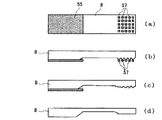
図24は、図1に示したようのコ字状の圧電基板8の製造方法を説明するためのフロー図である。このフロー図は、図24の左上隅に示したコ字状の圧電基板8を矢印方向から見た側面図を示している。図24(a)のように平板の矩形状の水晶基板51を洗浄・乾燥した後、同図(b)のように、真空装置の中に入れ、所定の温度に保ちながら蒸着、あるいはスパッタ等の方法で、水晶基板51の両主面にクロムを蒸着し、続いて金を蒸着し、クロム52と金53の薄膜を形成する。次に、図24(c)に示すようにクロムと金の薄膜52、53の上にレジスト膜54を塗布し、乾燥する。レジスト膜54を、マスクを介して露光、現像し、露光した部分のレジスト膜54剥離すると、図24(d)に示すようにレジスト膜54が所望の形状に加工される。次に金、クロムのエッチング液に夫々浸漬し、露呈した金属膜を剥離すると、図24(e)に示すようにエッチングする部分の金、クロム薄膜が除去される。これを水晶エッチング液中で所定の時間エッチングすると、図24(f)に示すように所望の形状にエッチングされる。レジスト膜54、金薄膜53、クロム膜52を剥離して、図24(g)に示すコ字状の圧電基板が得られる。水晶基板をエッチングすると結晶の異方性により、軸方向によりエッチング速度が異なり、若干尖った部分が生じる。ドライエッチングの場合は水晶基板に垂直に加工できる。   FIG. 24 is a flowchart for explaining a method of manufacturing the U-shaped piezoelectric substrate 8 as shown in FIG. This flowchart shows a side view of the U-shaped piezoelectric substrate 8 shown in the upper left corner of FIG. After washing and drying the flat rectangular quartz crystal substrate 51 as shown in FIG. 24A, it is placed in a vacuum apparatus as shown in FIG. In this way, chromium is vapor-deposited on both main surfaces of the quartz substrate 51, and then gold is vapor-deposited to form a thin film of chromium 52 and gold 53. Next, as shown in FIG. 24C, a resist film 54 is applied on the chromium and gold thin films 52 and 53 and dried. When the resist film 54 is exposed and developed through a mask and the exposed portion of the resist film 54 is peeled off, the resist film 54 is processed into a desired shape as shown in FIG. Next, when the exposed metal film is peeled off by immersing each in an etching solution of gold and chrome, the gold and chrome thin film at the portion to be etched is removed as shown in FIG. When this is etched in a crystal etching solution for a predetermined time, it is etched into a desired shape as shown in FIG. The resist film 54, the gold thin film 53, and the chromium film 52 are peeled off to obtain a U-shaped piezoelectric substrate shown in FIG. When the quartz substrate is etched, the etching rate varies depending on the axial direction due to the anisotropy of the crystal, and a slightly sharp portion is generated. In the case of dry etching, it can be processed perpendicular to the quartz substrate.

図25は、図8に示すようなコ字状の圧電基板8の一方の圧電片の中央部に凹陥部が形成され、両端部に肉厚部を有する圧電基板の製造方法を説明するフロー図である。図25(a)は、同図左上隅の圧電基板8の手前の圧電片を下面、A方向から見た平面図である。圧電片にレジスト膜を塗布し、マスクを介して露光し、エッチングする部分のレジスト膜を剥離し、エッチングをしない部分のレジスト膜、つまり、図25(a)に示すようなレジスト膜55、56、56、56は残す。図25(b)、(c)は、圧電基板8を側面B方向から見た図で、エッチング液に浸漬し、少しエッチングをすると、同図(b)のようにレジスト膜55、56、56、56が付着した圧電基板が得られる。この圧電基板を更にエッチング液中で所定の時間浸漬すると、図25(c)に示すような中央部に凹陥部が形成された圧電基板が得られる。   FIG. 25 is a flowchart for explaining a method of manufacturing a piezoelectric substrate in which a concave portion is formed at the center of one piezoelectric piece of the U-shaped piezoelectric substrate 8 as shown in FIG. It is. FIG. 25 (a) is a plan view of the piezoelectric piece in front of the piezoelectric substrate 8 at the upper left corner of the figure as seen from the lower surface and the A direction. A resist film is applied to the piezoelectric piece, exposed through a mask, the resist film in the part to be etched is peeled off, and the resist film in the part not to be etched, that is, resist films 55 and 56 as shown in FIG. , 56, 56 remain. FIGS. 25B and 25C are views of the piezoelectric substrate 8 as viewed from the side surface B. When the piezoelectric substrate 8 is immersed in an etching solution and etched slightly, the resist films 55, 56, and 56 are formed as shown in FIG. , 56 is obtained. When this piezoelectric substrate is further immersed in an etching solution for a predetermined time, a piezoelectric substrate having a recessed portion formed at the center as shown in FIG. 25C is obtained.

図26は長方形状の圧電基板の中央部に凹陥部を形成し、両端部の厚肉部が異なった厚さに形成する圧電基板の製造方法を示すフロー図である。図26(a)は裏面図、同図(b)〜(d)は側面図である。長方形状の圧電基板の全面にレジスト膜を塗布し、マスクを介して露光し、エッチングする部分のレジスト膜を剥離すると、図26(a)に示すように、一方の端にはレジスト55が所定の部分残り、他方の端にはレジスト膜57がドット状に残った圧電基板となる。この圧電基板を水晶エッチング液の中に浸漬すると、図26(b)の側面図ようにエッチングが進み、更にエッチングを継続すると同図(c)の側面図に示すように、ドット状のレジスト膜57が剥離した圧電基板となり、所定の時間エッチングすると同図(d)の側面図を示すような圧電基板が得られる。   FIG. 26 is a flow chart showing a method for manufacturing a piezoelectric substrate in which a concave portion is formed in the central portion of a rectangular piezoelectric substrate, and the thick portions at both ends are formed to have different thicknesses. FIG. 26 (a) is a back view, and FIGS. 26 (b) to (d) are side views. When a resist film is applied to the entire surface of the rectangular piezoelectric substrate, exposed through a mask, and the resist film to be etched is peeled off, a resist 55 is formed at one end as shown in FIG. This is a piezoelectric substrate in which the resist film 57 remains in the form of dots at the other end and the other end. When this piezoelectric substrate is immersed in a crystal etching solution, the etching proceeds as shown in the side view of FIG. 26B, and when the etching is continued, as shown in the side view of FIG. When the piezoelectric substrate 57 is peeled off and etched for a predetermined time, a piezoelectric substrate as shown in the side view of FIG.

上記の力検知ユニットと、発振回路61と、信号処理回路62、63と、力検知ユニット1、発振回路61、信号処理回路62、63を収容するハウジング60と、を備えた加速度センサを構成する。本発明の加速度センサは弾性表面波用いた力検知ユニットを使用するので、小型のみならず、薄型のセンサが得られ、更に1個の力検知ユニットで2軸方向の加速度が検知できる。   An acceleration sensor including the force detection unit, the oscillation circuit 61, the signal processing circuits 62 and 63, and the housing 60 that houses the force detection unit 1, the oscillation circuit 61, and the signal processing circuits 62 and 63 is configured. . Since the acceleration sensor of the present invention uses a force detection unit using a surface acoustic wave, not only a small sensor but also a thin sensor can be obtained, and further, a single force detection unit can detect acceleration in two axial directions.

本発明の第1の実施例の力検知ユニット1の構成を示した図であり、(a)は平面図、(b)(c)はQ1−Q1、Q2−Q2における断面図。It is the figure which showed the structure of the force detection unit 1 of the 1st Example of this invention, (a) is a top view, (b) (c) is sectional drawing in Q1-Q1, Q2-Q2. セラミックパッケージに収容した力検知ユニットを示す図。The figure which shows the force detection unit accommodated in the ceramic package. 力検知ユニット1の力無印加時の動作を説明する図。The figure explaining operation | movement at the time of no force application of the force detection unit 1. FIG. (a)(b)は力検知ユニット1の力印加時の動作を説明する図。(A) and (b) are the figures explaining the operation | movement at the time of the force application of the force detection unit 1. FIG. 第2の実施例の力検知ユニットのIDT電極構成を示す図。The figure which shows IDT electrode structure of the force detection unit of a 2nd Example. (a)(b)は夫々力検知ユニット1の力無印加時、力印加時の周波数応答を示す図。(A) and (b) are the figures which show the frequency response at the time of force application at the time of no force application of the force detection unit 1, respectively. (a)〜(e)は力検知ユニット1の出力の信号処理を説明する図。(A)-(e) is a figure explaining the signal processing of the output of the force detection unit 1. FIG. 第3の実施例の力検知ユニット構成を示す図であり、(a)は平面図、(b)(c)はQ1−Q1、Q2−Q2における断面図。It is a figure which shows the force detection unit structure of a 3rd Example, (a) is a top view, (b) (c) is sectional drawing in Q1-Q1, Q2-Q2. 第4の実施例の構成を示す図であり、(a)は平面図、(b)はQ1−Q1における断面図。It is a figure which shows the structure of a 4th Example, (a) is a top view, (b) is sectional drawing in Q1-Q1. 第4の実施例の力無印加時の周波数応答(実線)と、力印加時の周波数応答(破線)を示す図。The figure which shows the frequency response (solid line) at the time of no force application of a 4th Example, and the frequency response (dashed line) at the time of force application. 第5の実施例の構成を示す図であり、(a)は平面図、(b)はQ1−Q1における断面図。It is a figure which shows the structure of a 5th Example, (a) is a top view, (b) is sectional drawing in Q1-Q1. 第6の実施例の構成を示す断面図。Sectional drawing which shows the structure of a 6th Example. 第7の実施例の構成を示す断面図。Sectional drawing which shows the structure of a 7th Example. 第8の実施例の構成を示す図であり、(a)は平面図、(b)はQ1−Q1における断面図。It is a figure which shows the structure of the 8th Example, (a) is a top view, (b) is sectional drawing in Q1-Q1. 第9の実施例(金属膜が上)の構成を示す図であり、(a)は平面図、(b)はQ1−Q1における断面図。It is a figure which shows the structure of the 9th Example (a metal film is upper), (a) is a top view, (b) is sectional drawing in Q1-Q1. 第9の実施例(金属膜が下)の構成を示す断面図。Sectional drawing which shows the structure of a 9th Example (a metal film is below). 第10の実施例の構成を示す図であり、(a)は平面図、(b)はQ1−Q1における断面図。It is a figure which shows the structure of a 10th Example, (a) is a top view, (b) is sectional drawing in Q1-Q1. 第11の実施例の構成を示す図であり、(a)は平面図、(b)はQ1−Q1における断面図。It is a figure which shows the structure of the 11th Example, (a) is a top view, (b) is sectional drawing in Q1-Q1. 第12の実施例の構成を示す図であり、(a)は平面図、(b)はQ1−Q1における断面図。It is a figure which shows the structure of a 12th Example, (a) is a top view, (b) is sectional drawing in Q1-Q1. 第13の実施例の構成を示す図であり、(a)は平面図、(b)はQ1−Q1における断面図。It is a figure which shows the structure of 13th Example, (a) is a top view, (b) is sectional drawing in Q1-Q1. 第13の実施例の動作説明する図であり、(a)はZ軸方向に力が印加された時の状態を示す図、(b)はX軸方向に力が印加された時の状態を示す図。It is a figure explaining operation | movement of 13th Example, (a) is a figure which shows the state when force is applied to a Z-axis direction, (b) is a state when force is applied to an X-axis direction. FIG. 第14の実施例の構成を示す図であり、(a)は平面図、(b)はQ1−Q1における断面図。It is a figure which shows the structure of 14th Example, (a) is a top view, (b) is sectional drawing in Q1-Q1. 第15の実施例の構成を示す図であり、(a)は平面図、(b)はQ1−Q1における断面図。It is a figure which shows the structure of 15th Example, (a) is a top view, (b) is sectional drawing in Q1-Q1. (a)〜(g)はコ字状圧電基板の製造方法を説明するフロー図。(A)-(g) is a flowchart explaining the manufacturing method of a U-shaped piezoelectric substrate. (a)〜(c)は中央部に凹陥部を有する圧電基板を製造するフロー図。(A)-(c) is a flowchart which manufactures the piezoelectric substrate which has a recessed part in the center part. (a)〜(d)は中央部に凹陥部を有する圧電基板を製造するフロー図。(A)-(d) is a flowchart which manufactures the piezoelectric substrate which has a recessed part in the center part. 加速度センサの構成を示す斜視図。The perspective view which shows the structure of an acceleration sensor. 従来の外力センサの構成を示す側面図。The side view which shows the structure of the conventional external force sensor.

符号の説明Explanation of symbols

1、2、3、4、5、6 力検知ユニット、8 圧電基板、8a、8b 圧電片、8c、8c1、8c2 凹陥部、8d1、8d2、8e 厚肉部、9 連結支持部、10、11、12、13 IDT電極、15 グレーティング反射器、20a、20b、20c、20d、20e、20f ボンディングパッド、25 音波吸収材、30 接着剤、33 接合材、35 ボンディングワイヤ、40 金属部材、51 圧電基板、52 クロム、53 金、54、55、56 レジスト膜、P 支持基板、F 力、T 電極部   1, 2, 3, 4, 5, 6 Force detection unit, 8 Piezoelectric substrate, 8a, 8b Piezoelectric piece, 8c, 8c1, 8c2 Recessed part, 8d1, 8d2, 8e Thick part, 9 Connection support part, 10, 11 , 12, 13 IDT electrode, 15 grating reflector, 20a, 20b, 20c, 20d, 20e, 20f bonding pad, 25 sound absorbing material, 30 adhesive, 33 bonding material, 35 bonding wire, 40 metal member, 51 piezoelectric substrate , 52 Chrome, 53 Gold, 54, 55, 56 Resist film, P Support substrate, F force, T electrode

Claims (3)

平行な2本の細幅帯状の圧電片を連結支持部によりコ字状に一体化した圧電基板と、該2本の圧電片の各一方の主面から該連結支持部にかけて夫々形成された少なくとも送受一対のIDT電極と、を有した力感応素子と、
前記力感応素子の連結支持部の他方の主面側を接着保持する支持基板と、
を備えた力検知ユニットであって、
一方の前記圧電片に形成した前記送受一対のIDT電極と、
他方の前記圧電片に形成した前記送受一対のIDT電極と、
を夫々並列接続しており、
送信側IDT電極と受信側IDT電極との間の位相推移が、前記一方の前記圧電片に形成した前記送受一対のIDT電極と、前記他方の前記圧電片に形成した前記送受一対のIDT電極との間で、外力を加えない状態の時において互いに180°異なっていることを特徴とする力検知ユニット。
A piezoelectric substrate in which two parallel strips of piezoelectric strips are integrated in a U-shape by a connection support portion, and at least each formed from one main surface of the two piezoelectric pieces to the connection support portion. A force-sensitive element having a pair of transmitting and receiving IDT electrodes;
A support substrate for bonding and holding the other main surface side of the connection support portion of the force-sensitive element;
A force detection unit comprising:
A pair of IDT electrodes formed on one of the piezoelectric pieces;
A pair of transmitting and receiving IDT electrodes formed on the other piezoelectric piece;
Are connected in parallel,
The phase transition between the transmitting-side IDT electrode and the receiving-side IDT electrode is such that the pair of transmitting / receiving IDT electrodes formed on the one piezoelectric piece, and the pair of transmitting / receiving IDT electrodes formed on the other piezoelectric piece, The force detection unit is characterized by being different from each other by 180 ° when no external force is applied .
一方の前記圧電片及び前記連結支持部は、均一厚の厚肉部であり、
他方の前記圧電片は、前記厚肉部よりも薄い薄肉部を有していることを特徴とする請求項1に記載の力検知ユニット。
One of the piezoelectric pieces and the connection support part is a thick part having a uniform thickness,
The force detection unit according to claim 1, wherein the other piezoelectric piece has a thin portion thinner than the thick portion.
一方の前記圧電片及び前記連結支持部は、均一厚の厚肉部であり、他方の前記圧電片はその一方の主面の略中央部に凹陥部を形成することにより形成した薄肉部を有すると共に両端部に厚肉部を有していることを特徴とする請求項1に記載の力検知ユニット。   One of the piezoelectric pieces and the connection support part is a thick part having a uniform thickness, and the other piezoelectric piece has a thin part formed by forming a recessed part in a substantially central part of one main surface thereof. The force detection unit according to claim 1, further comprising thick portions at both ends.
JP2007128847A 2007-05-15 2007-05-15 Force detection unit Expired - Fee Related JP5018227B2 (en)

Priority Applications (1)

Application Number Priority Date Filing Date Title
JP2007128847A JP5018227B2 (en) 2007-05-15 2007-05-15 Force detection unit

Applications Claiming Priority (1)

Application Number Priority Date Filing Date Title
JP2007128847A JP5018227B2 (en) 2007-05-15 2007-05-15 Force detection unit

Related Child Applications (1)

Application Number Title Priority Date Filing Date
JP2011262665A Division JP2012042487A (en) 2011-11-30 2011-11-30 Force detection unit, method for manufacturing piezoelectric substrate, and acceleration sensor

Publications (2)

Publication Number Publication Date
JP2008286520A JP2008286520A (en) 2008-11-27
JP5018227B2 true JP5018227B2 (en) 2012-09-05

Family

ID=40146400

Family Applications (1)

Application Number Title Priority Date Filing Date
JP2007128847A Expired - Fee Related JP5018227B2 (en) 2007-05-15 2007-05-15 Force detection unit

Country Status (1)

Country Link
JP (1) JP5018227B2 (en)

Families Citing this family (11)

* Cited by examiner, † Cited by third party
Publication number Priority date Publication date Assignee Title
JP5135253B2 (en) * 2009-02-19 2013-02-06 株式会社東芝 Inertial sensor and inertial measuring device
JP4645923B2 (en) 2009-02-27 2011-03-09 セイコーエプソン株式会社 Surface acoustic wave resonator and surface acoustic wave oscillator
US8952596B2 (en) 2009-02-27 2015-02-10 Seiko Epson Corporation Surface acoustic wave resonator, surface acoustic wave oscillator, and electronic instrument
JP5678486B2 (en) 2010-06-17 2015-03-04 セイコーエプソン株式会社 Surface acoustic wave resonator, surface acoustic wave oscillator and electronic device
JP2012002679A (en) * 2010-06-17 2012-01-05 Tamagawa Seiki Co Ltd Inertial sensor
JP5934464B2 (en) 2010-08-26 2016-06-15 セイコーエプソン株式会社 Surface acoustic wave resonator, surface acoustic wave oscillator, and electronic device
JP2012049818A (en) 2010-08-26 2012-03-08 Seiko Epson Corp Surface acoustic wave resonator, surface acoustic wave oscillator, and electronic apparatus
JP2012049817A (en) 2010-08-26 2012-03-08 Seiko Epson Corp Surface acoustic wave device, surface acoustic wave oscillator, and electronic apparatus
JP2012060420A (en) 2010-09-09 2012-03-22 Seiko Epson Corp Surface acoustic wave device, electronic apparatus and sensor device
JP5849265B2 (en) * 2011-08-31 2016-01-27 多摩川精機株式会社 Surface acoustic wave type acceleration sensor and sensor element substrate
CN117957482A (en) * 2022-08-31 2024-04-30 京东方科技集团股份有限公司 Dimming module and dimming device

Family Cites Families (7)

* Cited by examiner, † Cited by third party
Publication number Priority date Publication date Assignee Title
FR2462695A1 (en) * 1979-07-27 1981-02-13 Thomson Csf SENSOR USING TWO TUNABLE OSCILLATORS CONNECTED TO A FREQUENCY MIXER COMPRISING A DEVICE FOR CALIBRATING THE FREQUENCY OF THE OUTPUT SIGNAL AND METHOD OF CALIBRATING THE FREQUENCY
JPS57196323U (en) * 1981-06-05 1982-12-13
JPH0641886B2 (en) * 1985-10-07 1994-06-01 アンリツ株式会社 SAW force sensor
JP2697887B2 (en) * 1989-03-02 1998-01-14 株式会社トキメック External force sensor using surface acoustic waves
JPH10197365A (en) * 1997-01-07 1998-07-31 Tokimec Inc External force sensor
JP4099505B2 (en) * 2003-11-27 2008-06-11 京セラ株式会社 Pressure sensor device
JP4511206B2 (en) * 2004-01-29 2010-07-28 京セラ株式会社 Pressure sensor module

Also Published As

Publication number Publication date
JP2008286520A (en) 2008-11-27

Similar Documents

Publication Publication Date Title
JP5018227B2 (en) Force detection unit
JP5375624B2 (en) Acceleration sensor and acceleration detection device
JP2008286521A (en) Rotational speed detecting unit, and rotational speed sensor
US8225662B2 (en) Acceleration sensing device
JP6031682B2 (en) Angular velocity sensor and detection element used therefor
JP2009042240A (en) Acceleration sensor
JP2012242343A (en) Acceleration sensor and acceleration detector
US20110259101A1 (en) Vibration-type force detection sensor and vibration-type force detection device
US20110221312A1 (en) Vibrator element, vibrator, sensor, and electronic apparatus
JP5013250B2 (en) Acceleration sensor
JP2009243981A (en) Surface acoustic wave sensor
JP2002122614A (en) Acceleration sensor
JP2004069562A (en) Capacitance type mechanical quantity sensor
JP3446732B2 (en) Acceleration sensor
WO2012098901A1 (en) Acceleration sensor
JP2002107373A (en) Acceleration sensor
JP2010181210A (en) Acceleration sensor
JP4420038B2 (en) Stress sensitive element
JP2012042487A (en) Force detection unit, method for manufacturing piezoelectric substrate, and acceleration sensor
JP4859649B2 (en) Angular velocity sensor
US9217642B2 (en) Vibrating gyroscope that prevents changes in sensitivity
JP2011169671A (en) Inertia sensor and inertia sensor device
JP2011059097A (en) Tuning fork vibrating reed, vibration sensor element, and vibration sensor
KR100870638B1 (en) Accelerometer using elastic wave and method for fabricating the same
JP4867858B2 (en) SAW sensor

Legal Events

Date Code Title Description
A621 Written request for application examination

Free format text: JAPANESE INTERMEDIATE CODE: A621

Effective date: 20100415

A711 Notification of change in applicant

Free format text: JAPANESE INTERMEDIATE CODE: A712

Effective date: 20110729

RD03 Notification of appointment of power of attorney

Free format text: JAPANESE INTERMEDIATE CODE: A7423

Effective date: 20110729

A521 Request for written amendment filed

Free format text: JAPANESE INTERMEDIATE CODE: A523

Effective date: 20110819

A977 Report on retrieval

Free format text: JAPANESE INTERMEDIATE CODE: A971007

Effective date: 20110826

A131 Notification of reasons for refusal

Free format text: JAPANESE INTERMEDIATE CODE: A131

Effective date: 20111004

A521 Request for written amendment filed

Free format text: JAPANESE INTERMEDIATE CODE: A523

Effective date: 20111130

RD03 Notification of appointment of power of attorney

Free format text: JAPANESE INTERMEDIATE CODE: A7423

Effective date: 20111130

TRDD Decision of grant or rejection written
A01 Written decision to grant a patent or to grant a registration (utility model)

Free format text: JAPANESE INTERMEDIATE CODE: A01

Effective date: 20120515

A01 Written decision to grant a patent or to grant a registration (utility model)

Free format text: JAPANESE INTERMEDIATE CODE: A01

A61 First payment of annual fees (during grant procedure)

Free format text: JAPANESE INTERMEDIATE CODE: A61

Effective date: 20120528

R150 Certificate of patent or registration of utility model

Free format text: JAPANESE INTERMEDIATE CODE: R150

FPAY Renewal fee payment (event date is renewal date of database)

Free format text: PAYMENT UNTIL: 20150622

Year of fee payment: 3

S531 Written request for registration of change of domicile

Free format text: JAPANESE INTERMEDIATE CODE: R313531

R350 Written notification of registration of transfer

Free format text: JAPANESE INTERMEDIATE CODE: R350

LAPS Cancellation because of no payment of annual fees