JP5014341B2 - Communication connector with bent contacts - Google Patents
Communication connector with bent contacts Download PDFInfo
- Publication number
- JP5014341B2 JP5014341B2 JP2008521659A JP2008521659A JP5014341B2 JP 5014341 B2 JP5014341 B2 JP 5014341B2 JP 2008521659 A JP2008521659 A JP 2008521659A JP 2008521659 A JP2008521659 A JP 2008521659A JP 5014341 B2 JP5014341 B2 JP 5014341B2
- Authority
- JP
- Japan
- Prior art keywords
- jack
- plug
- contact
- printed circuit
- flexible printed
- Prior art date
- Legal status (The legal status is an assumption and is not a legal conclusion. Google has not performed a legal analysis and makes no representation as to the accuracy of the status listed.)
- Expired - Fee Related
Links
Images


Classifications
-
- H—ELECTRICITY
- H05—ELECTRIC TECHNIQUES NOT OTHERWISE PROVIDED FOR
- H05K—PRINTED CIRCUITS; CASINGS OR CONSTRUCTIONAL DETAILS OF ELECTRIC APPARATUS; MANUFACTURE OF ASSEMBLAGES OF ELECTRICAL COMPONENTS
- H05K1/00—Printed circuits
- H05K1/02—Details
- H05K1/0213—Electrical arrangements not otherwise provided for
- H05K1/0216—Reduction of cross-talk, noise or electromagnetic interference
- H05K1/0228—Compensation of cross-talk by a mutually correlated lay-out of printed circuit traces, e.g. for compensation of cross-talk in mounted connectors
-
- H—ELECTRICITY
- H01—ELECTRIC ELEMENTS
- H01R—ELECTRICALLY-CONDUCTIVE CONNECTIONS; STRUCTURAL ASSOCIATIONS OF A PLURALITY OF MUTUALLY-INSULATED ELECTRICAL CONNECTING ELEMENTS; COUPLING DEVICES; CURRENT COLLECTORS
- H01R13/00—Details of coupling devices of the kinds covered by groups H01R12/70 or H01R24/00 - H01R33/00
- H01R13/646—Details of coupling devices of the kinds covered by groups H01R12/70 or H01R24/00 - H01R33/00 specially adapted for high-frequency, e.g. structures providing an impedance match or phase match
- H01R13/6461—Means for preventing cross-talk
- H01R13/6464—Means for preventing cross-talk by adding capacitive elements
- H01R13/6466—Means for preventing cross-talk by adding capacitive elements on substrates, e.g. printed circuit boards [PCB]
-
- H—ELECTRICITY
- H01—ELECTRIC ELEMENTS
- H01R—ELECTRICALLY-CONDUCTIVE CONNECTIONS; STRUCTURAL ASSOCIATIONS OF A PLURALITY OF MUTUALLY-INSULATED ELECTRICAL CONNECTING ELEMENTS; COUPLING DEVICES; CURRENT COLLECTORS
- H01R13/00—Details of coupling devices of the kinds covered by groups H01R12/70 or H01R24/00 - H01R33/00
- H01R13/66—Structural association with built-in electrical component
- H01R13/665—Structural association with built-in electrical component with built-in electronic circuit
- H01R13/6658—Structural association with built-in electrical component with built-in electronic circuit on printed circuit board
-
- H—ELECTRICITY
- H01—ELECTRIC ELEMENTS
- H01R—ELECTRICALLY-CONDUCTIVE CONNECTIONS; STRUCTURAL ASSOCIATIONS OF A PLURALITY OF MUTUALLY-INSULATED ELECTRICAL CONNECTING ELEMENTS; COUPLING DEVICES; CURRENT COLLECTORS
- H01R24/00—Two-part coupling devices, or either of their cooperating parts, characterised by their overall structure
- H01R24/60—Contacts spaced along planar side wall transverse to longitudinal axis of engagement
- H01R24/62—Sliding engagements with one side only, e.g. modular jack coupling devices
- H01R24/64—Sliding engagements with one side only, e.g. modular jack coupling devices for high frequency, e.g. RJ 45
-
- H—ELECTRICITY
- H05—ELECTRIC TECHNIQUES NOT OTHERWISE PROVIDED FOR
- H05K—PRINTED CIRCUITS; CASINGS OR CONSTRUCTIONAL DETAILS OF ELECTRIC APPARATUS; MANUFACTURE OF ASSEMBLAGES OF ELECTRICAL COMPONENTS
- H05K1/00—Printed circuits
- H05K1/18—Printed circuits structurally associated with non-printed electric components
- H05K1/189—Printed circuits structurally associated with non-printed electric components characterised by the use of a flexible or folded printed circuit
-
- H—ELECTRICITY
- H05—ELECTRIC TECHNIQUES NOT OTHERWISE PROVIDED FOR
- H05K—PRINTED CIRCUITS; CASINGS OR CONSTRUCTIONAL DETAILS OF ELECTRIC APPARATUS; MANUFACTURE OF ASSEMBLAGES OF ELECTRICAL COMPONENTS
- H05K2201/00—Indexing scheme relating to printed circuits covered by H05K1/00
- H05K2201/10—Details of components or other objects attached to or integrated in a printed circuit board
- H05K2201/10007—Types of components
- H05K2201/10189—Non-printed connector
-
- Y—GENERAL TAGGING OF NEW TECHNOLOGICAL DEVELOPMENTS; GENERAL TAGGING OF CROSS-SECTIONAL TECHNOLOGIES SPANNING OVER SEVERAL SECTIONS OF THE IPC; TECHNICAL SUBJECTS COVERED BY FORMER USPC CROSS-REFERENCE ART COLLECTIONS [XRACs] AND DIGESTS
- Y10—TECHNICAL SUBJECTS COVERED BY FORMER USPC
- Y10S—TECHNICAL SUBJECTS COVERED BY FORMER USPC CROSS-REFERENCE ART COLLECTIONS [XRACs] AND DIGESTS
- Y10S439/00—Electrical connectors
- Y10S439/941—Crosstalk suppression
Landscapes
- Engineering & Computer Science (AREA)
- Microelectronics & Electronic Packaging (AREA)
- Physics & Mathematics (AREA)
- Electromagnetism (AREA)
- Details Of Connecting Devices For Male And Female Coupling (AREA)
- Coupling Device And Connection With Printed Circuit (AREA)
Abstract
Description
[0001] 本出願は、2005年7月15日付けで出願された米国仮特許出願番号60/699,823の利益を主張するものである。本出願は、2004年12月15日付けで出願された米国特許出願番号11/014,097、2005年2月20日付けで出願された米国特許出願番号11/055,344、2005年3月11日付けで出願された米国特許出願番号11/078,816、2005年4月5日付けで出願された米国特許出願番号11/099,110、2004年7月13日付けで出願された米国仮特許出願番号60/587,416、2004年12月17日付けで出願された米国仮特許出願番号60/637,024の内容の全体を参考として引用し本明細書に含めるものである。
[0001] This application claims the benefit of US Provisional Patent Application No. 60 / 699,823, filed July 15, 2005. This application is filed on U.S. Patent Application No. 11 / 014,097 filed December 15, 2004, U.S. Patent Application No. 11 / 055,344, filed Feb. 20, 2005, March 2005. United States Patent Application No. 11 / 078,816, filed on the 11th, United States Patent Application No. 11 / 099,110, filed on the 5th April 2005, US filed on the 13th July 2004 The entire contents of provisional
[0002] 本発明は、全体として、電気コネクタ、より詳細には、フレキシブルプリント回路に固定された端曲げした接点を有する通信ジャックに関する。 [0002] The present invention relates generally to electrical connectors, and more particularly to communication jacks having end-bent contacts secured to a flexible printed circuit.
[0003] 通信業界において、データの伝送速度が不断に増大するに伴い、ジャック及び(又は)プラグ内の近接して隔てた平行な導体間にて容量結合及び誘導結合に起因するクロストークが益々、問題となっている。クロストーク性能が改良されたモジュラーコネクタは、益々、増大する要求基準に適合するよう設計されている。これらの改良されたコネクタの多くは、その内容の全体を参考として引用し本明細書に含めた、米国特許番号5,997,358に開示された着想を含んでいる。特に、最近のコネクタは、不愉快な近端クロストーク(NEXT)を打ち消すため所定の量のクロストーク補償技術を採用している。補償領域とプラグ/ジャックのインターフェースとの間の距離に起因する伝搬遅延からの位相偏移に対処するため2つ又はより多くの補償段階が使用される。その結果、不愉快なクロストークの大きさ及び位相は、全体として、等しい大きさであるが、反対の位相を有する補償により相殺される。 [0003] In the telecommunications industry, as data transmission rates continue to increase, crosstalk due to capacitive and inductive coupling between closely spaced parallel conductors in jacks and / or plugs is increasing. , Has become a problem. Modular connectors with improved crosstalk performance are designed to meet increasingly demanding requirements. Many of these improved connectors include the idea disclosed in US Pat. No. 5,997,358, which is incorporated herein by reference in its entirety. In particular, modern connectors employ a predetermined amount of crosstalk compensation technology to counteract unpleasant near-end crosstalk (NEXT). Two or more compensation stages are used to address the phase shift from propagation delay due to the distance between the compensation region and the plug / jack interface. As a result, the unpleasant crosstalk magnitude and phase as a whole are equal but offset by compensation having opposite phases.
[0004] 500MHz以上のものを含む、近年の伝送速度は、´358特許に開示された技術の能力を上回っている。このため、改良された補償技術が必要とされている。 [0004] Recent transmission rates, including those above 500 MHz, exceed the capabilities of the technology disclosed in the '358 patent. For this reason, improved compensation techniques are needed.
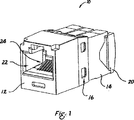
[0023] 図1は、本発明の1つの実施の形態に従った通信ジャック10の斜視図である。ジャック10は、主ジャックハウジング12と、例えば、ハウジングクリップ16を介して主ジャックハウジング12に装着された後部ジャックハウジング14とを含む。後部ジャックハウジング14には、圧接部(insulation−displacement contacts)IDCs)18(図2に図示)用の通路が設けられている。ワイヤーキャップ20は、撚った対の通信ケーブルに対するインターフェースを提供する。これと代替的に、パンチダウンブロックを通信ジャック10内に組み込むことができる。主ジャックハウジング12は、通信プラグを受け入れる受容部22を備え、受容部22内のプラグインターフェース接点24は、プラグの接点と接触する。
[0023] FIG. 1 is a perspective view of a communication jack 10 according to one embodiment of the present invention. The jack 10 includes a
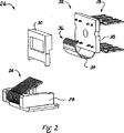
[0024] プラグインターフェース接点24は、図2に示した接点キャリア組立体26内に保持されている。接点キャリア組立体26は、接点スレッド28と、プリント回路板(PCB)32を保持し得るようにされた垂直支持体30とを備えている。プリント回路板32は、プラグインターフェース接点24に装着するためのジャック接点箇所36を有するフレキシブル部分34を備えている。PCB32は、IDCs18が電気的に且つ機械的に装着される(例えば、順応性ピンを介して)剛性な部分38を更に備えている。PCB32は、プラグインターフェース接点24とIDCs18との間の電気的接続部を提供し、通信ジャック10を通って伝わる通信信号に対するクロストークの補償を更に可能にする。
[0024] The
[0025] PCB32のフレキシブル部分34の平面図が図3に示されている。ジャック接点箇所36aないし36hは、第1ないし第8のプラグインターフェース接点24に対して相応する。第1ないし第8のジャック接点箇所36a−36hの各々は、PCB32上に相応する導電性トレース1ないし8を有する。図3の平面図において、フレキシブル部分34の頂部に沿った導電性トレースは、実線で示され、フレキシブル部分34の底部に沿った導電性トレースは、破線で示されている。
[0025] A top view of the
[0026] PCB32の補償回路は、2005年3月11日付けで出願された出願係属中の米国特許出願番号11/078,816に示した分割と場合と同様に、領域に分割されている。詳細には、本発明の補償回路は、´816特許出願に記載されたように、6つの領域A−Fに分割され、また、第7の領域、すなわち領域Gを更に含む。
[0026] The compensation circuit for
[0027] 領域Aは、ジャック接点箇所36aないし36hから近端クロストーク(NEXT)補償領域への転移領域である。
[0028] 領域Bは、NEXT補償領域である。
[0029] 領域Cは、NEXT補償領域からNEXTクロストーク領域への転移領域である。
[0027] Region A is a transition region from the jack contact points 36a to 36h to the near-end crosstalk (NEXT) compensation region.
[0028] Region B is a NEXT compensation region.
[0029] Region C is a transition region from the NEXT compensation region to the NEXT crosstalk region.
[0030] 領域Dは、ジャック接点を補償する補償領域である。
[0031] 領域Eは、NEXTクロストーク領域である。
[0032] 領域Fは、図8に示したように、NEXTクロストーク領域をIDCソケット40と接続する中立領域である。
[0033] 領域Gは、周波数が増すに伴い、NEXT補償を減少させる可変の補償領域である。
[0030] Region D is a compensation region that compensates for jack contacts.
[0031] Region E is a NEXT crosstalk region.
[0032] The region F is a neutral region that connects the NEXT crosstalk region to the IDC
[0033] Region G is a variable compensation region that reduces NEXT compensation as the frequency increases.
[0034] 図3には、領域A、B、C及びEのおおよその長さがインチで示されている。
[0035] 領域B、D、F内にて、一部の導電性トレースは、導体間にて容量補償を許容する容量型板を有している。これらの容量結合は、図3にて、「Cx、y」として標識されており、ここで、xは、フレキシブル部分34の頂部に沿った相応する導電性トレースであり、yは、該結合部にて容量結合されるフレキシブル部分34の底部に沿った相応する導電性トレースである。例えば、図3に示したように、C2、5は、頂部における第二の導電性トレースと、底部における第五の導電性トレースとの間の容量結合である。
[0034] In FIG. 3, the approximate lengths of regions A, B, C, and E are shown in inches.
[0035] Within regions B, D, and F, some conductive traces have capacitive plates that allow capacitance compensation between conductors. These capacitive couplings are labeled in FIG. 3 as “C x, y ”, where x is the corresponding conductive trace along the top of the
[0036] 第1、第7、第8を除く導電性トレースの全ては、図3ないし図5に示したように、導電性バイアス46aないし46gを通してフレキシブル部分34の頂部と底部との間にて信号を伝達する。
[0036] All of the conductive traces except the first, seventh, and eighth are between the top and bottom of the
[0037] 本発明のPCB32のフレキシブル部分34は、通信ジャック10内の6接点プラグ又は8接点プラグを使用することを受け入れるのを助ける追加的な作用部を含む。図3に示し且つ、以下により詳細に説明するように、第1及び第8のジャック接点箇所36a、36hに対する細長い接続伸長部42a、42hが設けられる。更に、第一のスリット44a及び第二のスリット44bがフレキシブル部分34に切り込まれて、細長い接続伸長部42a、42hが第2ないし第7のジャック接点箇所36b、36gの接続伸長部よりも一層、曲がることを許容する。
[0037] The
[0038] 図6及び図7には、図3の線6−6、7−7に沿ったフレキシブル部分34の断面図がそれぞれ示されている。図6には、第1のジャック接点箇所36aが第1のプラグインターフェース接点24と接続された、接点箇所バイアス48の断面図が示されている。断面図には、例えば、カプトン(KAPTON)ポリイミドフィルムにて製造されたフレキシブルコア50が示されている。接点パッド52は、ジャック接点箇所36の領域内にて頂部層及び底部層に沿って設けられている。バイアス48は、導電性であり、また、銅めっきすることができる。図7には、図3に示したように、第一の導体及び第二の導体とそれぞれ関係した接続伸長部42a、42bの断面図が示されている。断面図の各々には、フレキシブルコアが示されている。第一の導体と関係したトレース1は、図7の底部層に示され、第二の導体と関係したトレース2は、頂部層に示されている。
[0038] FIGS. 6 and 7 show cross-sectional views of the
[0039] 図8は、フレキシブル部分34と、剛性な部分38とを示すプリント回路板32の平面図である。剛性な部分は、IDCソケット40と、領域Fの導電性トレースとを含む。
[0039] FIG. 8 is a plan view of the printed
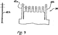
[0040]次に、図9及び図10を参照すると、2つの概略図には、PCBのフレキシブル部分34は6導体プラグ及び8導体プラグの双方を受け入れ得るようにされていることが示されている。米国特許出願番号11/078,816に記載され且つ図10に更に示されたように、プラグ−ジャックインターフェースは、プラグインターフェース接点24とフレキシブル回路板(又は回路板のフレキシブル部分)との間の接点の真上に配設されている。これらの接点位置は、プラグが装着されないとき(図11及び図12に示したように)又は標準的な8接点プラグが装着されるとき、ほぼ直線上に配置される。しかし、6接点プラグが装着されるとき(図13及び図14に図示)、接点1及び8は接点2ないし7よりも偏向する。
[0040] Referring now to FIGS. 9 and 10, two schematic diagrams show that the
[0041] トレース1、8をジャック接点1、8と接続する領域Aの接続伸長部42a、42hは、図9に示したように長くされており、また、6接点プラグがジャック内に装着されたとき、接点1、8が接点2ないし7の偏向と比較して、更に偏向するのを容易にし得るよう、図10に示したように「S字形」曲がり部が含められている。
[0041] The
[0042] 図13及び図14に示したように、第8のトレースと関係したより長い接続伸長部42hは、6接点プラグが受容部22内に挿入されたとき、プラグインターフェース接点24h(第8の導体と関係した)がより大きく偏向することを許容する。
[0042] As shown in FIGS. 13 and 14, the
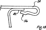
[0043] プラグ−ジャックインターフェース54に隣接し且つ該インターフェース54の反対側部にてPCB32のフレキシブル部分34をプラグインターフェース接点24と機械的に且つ電気的に接続する好ましい設計が図15ないし図17に示されている。この接続は、図15に示したように、プラグインターフェース接点24の自由な先端56を折り曲げることにより、また、PCB32のフレキシブル部分34の接続伸長部42に隣接して各接点の2つの部分58、60を互いにスポット溶接することにより形成される。接続伸長部42は、各接点の2つの部分58、60の間にて挟持される。図16及び図17に示したようなスポット溶接ステップは、溶接電極62a、62bを使用して実行することができる。
[0043] A preferred design for mechanically and electrically connecting the
[0044]上述したように、接点を端曲げし且つ溶接することは、プラグインターフェース接点が接続伸長部42を把持するのを許容する摩擦力を提供する。図18に示したように、プラグインターフェース接点24には、これらの接点がプラグ−ジャックインターフェース54の下方にて接点箇所バイアス48と接触する領域内にて把持作用部64を設けることができる。バイアス48上のプラグインターフェース接点24の把持は、接点24上にて接点をコイニング加工し、鋸歯状に加工し又は研磨し若しくは歯部をロール成形するといったような多数の方法により向上させることができる。
[0044] As described above, bending and welding the contacts provides a frictional force that allows the plug interface contacts to grip the
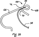
[0045] 図19及び図20には、フレキシブルプリント回路板又は回路板のフレキシブル部分34をジャック接点と接続する1つの代替的な方法が示されている。この実施の形態において、ジャック接点は、第一の曲がり部68と、第二の曲がり部70とが設けられたクリップ接点66である。回路板のフレキシブル部分34の接続伸長部42は、クリップ接点66の第二の曲がり部70とクリップ接点の直線状部分72との間の摩擦によりプラグ−ジャックインターフェースの下方に保持されている。
[0046] PCBのフレキシブル部分をプラグインターフェース接点と接続することに関して上記に説明したが、この接続方法は、剛性な部分を含まないフレキシブルプリント回路(FPCs)と共に使用することも可能であることを理解すべきである。
[0045] FIGS. 19 and 20 illustrate one alternative method of connecting the flexible printed circuit board or
[0046] Although described above with respect to connecting a flexible portion of a PCB with a plug interface contact, it is understood that this connection method can also be used with flexible printed circuits (FPCs) that do not include a rigid portion. Should.
[0047] 本発明の特に好ましい実施の形態について示し且つ説明したが、当該技術の当業者には、本発明の教示から逸脱せずに変更及び改変例が具体化可能であることは明らかであろう。上記の説明及び添付図面に示した事項は、単に説明のためにのみ記載したものであり、限定的なものではない。 [0047] While particularly preferred embodiments of the invention have been shown and described, it would be obvious to those skilled in the art that changes and modifications can be implemented without departing from the teachings of the invention. Let's go. The matters described in the above description and the accompanying drawings are provided for illustrative purposes only and are not limiting.
Claims (2)
Applications Claiming Priority (5)
| Application Number | Priority Date | Filing Date | Title |
|---|---|---|---|
| US69982305P | 2005-07-15 | 2005-07-15 | |
| US60/699,823 | 2005-07-15 | ||
| US11/457,171 | 2006-07-13 | ||
| US11/457,171 US7357683B2 (en) | 2005-07-15 | 2006-07-13 | Communications connector with crimped contacts |
| PCT/US2006/027473 WO2007011772A2 (en) | 2005-07-15 | 2006-07-13 | Commumications connector with crosstalk compensation apparatus |
Related Child Applications (1)
| Application Number | Title | Priority Date | Filing Date |
|---|---|---|---|
| JP2011264951A Division JP5209775B2 (en) | 2005-07-15 | 2011-12-02 | Crosstalk compensation device |
Publications (2)
| Publication Number | Publication Date |
|---|---|
| JP2009502009A JP2009502009A (en) | 2009-01-22 |
| JP5014341B2 true JP5014341B2 (en) | 2012-08-29 |
Family
ID=37390904
Family Applications (2)
| Application Number | Title | Priority Date | Filing Date |
|---|---|---|---|
| JP2008521659A Expired - Fee Related JP5014341B2 (en) | 2005-07-15 | 2006-07-13 | Communication connector with bent contacts |
| JP2011264951A Expired - Fee Related JP5209775B2 (en) | 2005-07-15 | 2011-12-02 | Crosstalk compensation device |
Family Applications After (1)
| Application Number | Title | Priority Date | Filing Date |
|---|---|---|---|
| JP2011264951A Expired - Fee Related JP5209775B2 (en) | 2005-07-15 | 2011-12-02 | Crosstalk compensation device |
Country Status (7)
| Country | Link |
|---|---|
| US (2) | US7357683B2 (en) |
| EP (2) | EP2390967B1 (en) |
| JP (2) | JP5014341B2 (en) |
| CN (1) | CN101223677B (en) |
| AT (1) | ATE537586T1 (en) |
| TW (1) | TWI389393B (en) |
| WO (1) | WO2007011772A2 (en) |
Families Citing this family (49)
| Publication number | Priority date | Publication date | Assignee | Title |
|---|---|---|---|---|
| US7479043B2 (en) * | 2006-05-08 | 2009-01-20 | The Siemon Company | Targeted compensation in telecommunications connectors |
| CN101584089B (en) | 2006-12-13 | 2012-06-13 | 泛达公司 | Communication jack having layered plug interface contacts |
| US7427218B1 (en) * | 2007-05-23 | 2008-09-23 | Commscope, Inc. Of North Carolina | Communications connectors with staggered contacts that connect to a printed circuit board via contact pads |
| EP2191541B1 (en) * | 2007-09-19 | 2020-04-29 | Leviton Manufacturing Co., Inc. | Internal crosstalk compensation circuit formed on a flexible printed circuit board positioned within a communications outlet, and methods and systems relating to same |
| US7736195B1 (en) | 2009-03-10 | 2010-06-15 | Leviton Manufacturing Co., Inc. | Circuits, systems and methods for implementing high speed data communications connectors that provide for reduced modal alien crosstalk in communications systems |
| US7967645B2 (en) * | 2007-09-19 | 2011-06-28 | Leviton Manufacturing Co., Inc. | High speed data communications connector circuits, systems, and methods for reducing crosstalk in communications systems |
| US7780480B2 (en) * | 2008-02-08 | 2010-08-24 | Panduit Corp. | Communications connector with improved contacts |
| US10334735B2 (en) | 2008-02-14 | 2019-06-25 | Metrospec Technology, L.L.C. | LED lighting systems and methods |
| US8143631B2 (en) | 2008-03-06 | 2012-03-27 | Metrospec Technology Llc | Layered structure for use with high power light emitting diode systems |
| US11266014B2 (en) | 2008-02-14 | 2022-03-01 | Metrospec Technology, L.L.C. | LED lighting systems and method |
| US8007286B1 (en) | 2008-03-18 | 2011-08-30 | Metrospec Technology, Llc | Circuit boards interconnected by overlapping plated through holes portions |
| US8851356B1 (en) | 2008-02-14 | 2014-10-07 | Metrospec Technology, L.L.C. | Flexible circuit board interconnection and methods |
| US7686649B2 (en) * | 2008-06-06 | 2010-03-30 | Tyco Electronics Corporation | Electrical connector with compensation component |
| FR2934425B1 (en) * | 2008-07-28 | 2021-07-30 | Legrand France | INSERT AND ASSEMBLY METHOD OF SUCH AN INSERT. |
| WO2010025214A1 (en) * | 2008-08-28 | 2010-03-04 | Molex Incorporated | Connector with overlapping ground configuration |
| US8202128B2 (en) * | 2008-11-25 | 2012-06-19 | Adc Gmbh | Telecommunications jack with adjustable crosstalk compensation |
| US7794286B2 (en) * | 2008-12-12 | 2010-09-14 | Hubbell Incorporated | Electrical connector with separate contact mounting and compensation boards |
| WO2011005972A1 (en) * | 2009-07-10 | 2011-01-13 | Panduit Corp. | Communications connector with a short conductive path to compensation |
| US7967644B2 (en) * | 2009-08-25 | 2011-06-28 | Tyco Electronics Corporation | Electrical connector with separable contacts |
| US8016621B2 (en) | 2009-08-25 | 2011-09-13 | Tyco Electronics Corporation | Electrical connector having an electrically parallel compensation region |
| US8128436B2 (en) * | 2009-08-25 | 2012-03-06 | Tyco Electronics Corporation | Electrical connectors with crosstalk compensation |
| US8435082B2 (en) | 2010-08-03 | 2013-05-07 | Tyco Electronics Corporation | Electrical connectors and printed circuits having broadside-coupling regions |
| US7850492B1 (en) * | 2009-11-03 | 2010-12-14 | Panduit Corp. | Communication connector with improved crosstalk compensation |
| US9627816B2 (en) | 2012-02-13 | 2017-04-18 | Sentinel Connector System Inc. | High speed grounded communication jack |
| US9653847B2 (en) | 2013-01-11 | 2017-05-16 | Sentinel Connector System, Inc. | High speed communication jack |
| US9337592B2 (en) | 2012-02-13 | 2016-05-10 | Sentinel Connector Systems, Inc. | High speed communication jack |
| US8858266B2 (en) * | 2012-02-13 | 2014-10-14 | Sentinel Connector Systems, Inc. | High speed communication jack |
| US8961239B2 (en) | 2012-09-07 | 2015-02-24 | Commscope, Inc. Of North Carolina | Communication jack having a plurality of contacts mounted on a flexible printed circuit board |
| US8858267B2 (en) * | 2013-03-14 | 2014-10-14 | Commscope, Inc. Of North Carolina | Communications plugs and patch cords with mode conversion control circuitry |
| US9246274B2 (en) * | 2013-03-15 | 2016-01-26 | Panduit Corp. | Communication connectors having crosstalk compensation networks |
| US9088106B2 (en) * | 2013-05-14 | 2015-07-21 | Commscope, Inc. Of North Carolina | Communications jacks having flexible printed circuit boards with common mode crosstalk compensation |
| DE102013108130A1 (en) * | 2013-07-30 | 2015-02-05 | MCQ TECH GmbH | Contact set for a connection socket |
| DE102013114651A1 (en) * | 2013-12-20 | 2015-06-25 | Phoenix Contact Gmbh & Co. Kg | Loop bridge for looping through a number of electrical signals |
| EP2942837B1 (en) * | 2014-05-06 | 2019-07-03 | ODU GmbH & Co KG. | Connector assembly with flexible circuit board |
| DE102014111049A1 (en) * | 2014-08-04 | 2016-02-04 | Wilhelm Rutenbeck Gmbh & Co. Kg | Socket for telecommunications and / or data transmission systems |
| EP3201995A4 (en) | 2014-10-01 | 2018-06-06 | Sentinel Connector Systems Inc. | High speed communication jack |
| US9966703B2 (en) | 2014-10-17 | 2018-05-08 | Panduit Corp. | Communication connector |
| US10050383B2 (en) * | 2015-05-19 | 2018-08-14 | Panduit Corp. | Communication connectors |
| US9912083B2 (en) | 2015-07-21 | 2018-03-06 | Sentinel Connector Systems, Inc. | High speed plug |
| DE102015120788A1 (en) | 2015-11-30 | 2017-06-01 | Phoenix Contact Gmbh & Co. Kg | loop bridge |
| JP7028517B2 (en) * | 2015-12-01 | 2022-03-02 | センティネル コネクター システムズ,インコーポレイテッド | High-speed communication jack |
| US20170317450A1 (en) * | 2016-04-29 | 2017-11-02 | Panduit Corp. | RJ Communication Connectors |
| WO2017192848A1 (en) | 2016-05-04 | 2017-11-09 | Sentinel Connector Systems, Inc. | Large conductor industrial plug |
| WO2018081712A1 (en) | 2016-10-31 | 2018-05-03 | Commscope Technologies Llc | Connector with capacitive crosstalk compensation |
| US10798819B2 (en) * | 2016-10-31 | 2020-10-06 | Commscope, Inc. Of North Carolina | Flexible printed circuit to mitigate cracking at through-holes |
| US10361514B2 (en) * | 2017-03-02 | 2019-07-23 | Panduit Corp. | Communication connectors utilizing multiple contact points |
| USD857006S1 (en) * | 2017-06-30 | 2019-08-20 | Vince DeVito | Polarized modular telephone jack |
| US10673184B2 (en) * | 2018-03-27 | 2020-06-02 | Veoneer Us Inc. | Rigid electrical connection to strain sensitive sensing component |
| US10849200B2 (en) | 2018-09-28 | 2020-11-24 | Metrospec Technology, L.L.C. | Solid state lighting circuit with current bias and method of controlling thereof |
Family Cites Families (29)
| Publication number | Priority date | Publication date | Assignee | Title |
|---|---|---|---|---|
| US1409704A (en) | 1921-01-17 | 1922-03-14 | Silvio A Gizzi | Pad for shoe soles |
| US4777240A (en) | 1984-03-08 | 1988-10-11 | Scripps Clinic And Research Foundation | SV40 expression vector containing HBxAg as an expression marker |
| JPH0665090B2 (en) | 1985-09-06 | 1994-08-22 | FPC connector | |
| US5692925A (en) | 1986-07-23 | 1997-12-02 | Virginia Patent Development Corporation | Modular plug comprising circuit elements |
| JPH0455421Y2 (en) | 1986-11-28 | 1992-12-25 | ||
| JPH0353767U (en) * | 1989-09-26 | 1991-05-24 | ||
| FR2705500B1 (en) | 1993-05-14 | 1995-08-18 | Proner Comatel Sa | Electrical connection device and corresponding manufacturing method. |
| US5647767A (en) | 1995-02-06 | 1997-07-15 | The Whitaker Corporation | Electrical connector jack assembly for signal transmission |
| CA2182438C (en) | 1996-07-31 | 2001-05-29 | Peter Craig | Circuit connector |
| US5997358A (en) * | 1997-09-02 | 1999-12-07 | Lucent Technologies Inc. | Electrical connector having time-delayed signal compensation |
| US6231397B1 (en) * | 1998-04-16 | 2001-05-15 | Thomas & Betts International, Inc. | Crosstalk reducing electrical jack and plug connector |
| TW389006B (en) | 1998-11-20 | 2000-05-01 | Hon Hai Prec Inductry Co Ltd | Method of assembling electric device and using electric elements and product thereof |
| US6354865B1 (en) * | 1998-12-17 | 2002-03-12 | Tyco Electronics Logistics Ag | Modular electrical plug including a printed circuit substrate |
| US6179668B1 (en) | 1999-06-22 | 2001-01-30 | Chin-Mao Kan | Electric connector including a circuit board |
| US6179669B1 (en) * | 1999-07-12 | 2001-01-30 | Thomas Shiaw-Cherng Chiang | Molded receptacle for a daisy chain power cord assembly |
| US6533588B1 (en) | 2000-03-30 | 2003-03-18 | Delphi Technologies, Inc. | Connector assembly for flexible circuits |
| JP4327328B2 (en) | 2000-04-04 | 2009-09-09 | ローム株式会社 | Electrical connection structure of circuit board and flexible flat cable |
| US6855013B2 (en) | 2000-05-08 | 2005-02-15 | Tyco Electronic Logistics Ag | LCD connector for printed circuit boards |
| TW458424U (en) * | 2000-10-20 | 2001-10-01 | Hon Hai Prec Ind Co Ltd | Cable connector assembly |
| DE50115867D1 (en) * | 2000-11-20 | 2011-06-16 | Tyco Electronics Amp Gmbh | Electrical connector for flexible flat cables or flexible printed circuit boards |
| US6547597B2 (en) | 2001-07-10 | 2003-04-15 | Littelfuse, Inc. | Apparatus and method for incorporating surface mount components into connectors |
| US6729913B2 (en) | 2001-09-07 | 2004-05-04 | Rockwell Automation Technologies, Inc. | Network branch connector and method and system incorporating same |
| US6881096B2 (en) * | 2002-04-15 | 2005-04-19 | Lantronix, Inc. | Compact serial-to-ethernet conversion port |
| US7265300B2 (en) | 2003-03-21 | 2007-09-04 | Commscope Solutions Properties, Llc | Next high frequency improvement using hybrid substrates of two materials with different dielectric constant frequency slopes |
| EP1723702B1 (en) * | 2004-03-12 | 2015-10-28 | Panduit Corporation | Methods and apparatus for reducing crosstalk in electrical connectors |
| EP1774625B1 (en) * | 2004-07-13 | 2014-06-25 | Panduit Corporation | Communications connector with flexible printed circuit board |
| US7204722B2 (en) * | 2004-12-07 | 2007-04-17 | Commscope Solutions Properties, Llc | Communications jack with compensation for differential to differential and differential to common mode crosstalk |
| US7881605B2 (en) | 2007-03-02 | 2011-02-01 | Nikon Corporation | Camera with built-in projector and projector device |
| US9911005B2 (en) | 2016-03-18 | 2018-03-06 | International Business Machines Corporation | Protecting search privacy using policy-based search terms |
-
2006
- 2006-07-13 EP EP11178247A patent/EP2390967B1/en not_active Not-in-force
- 2006-07-13 CN CN200680025531XA patent/CN101223677B/en not_active Expired - Fee Related
- 2006-07-13 EP EP06787386A patent/EP1911131B1/en not_active Not-in-force
- 2006-07-13 WO PCT/US2006/027473 patent/WO2007011772A2/en active Application Filing
- 2006-07-13 US US11/457,171 patent/US7357683B2/en active Active
- 2006-07-13 AT AT06787386T patent/ATE537586T1/en active
- 2006-07-13 JP JP2008521659A patent/JP5014341B2/en not_active Expired - Fee Related
- 2006-07-17 TW TW095126082A patent/TWI389393B/en not_active IP Right Cessation
-
2008
- 2008-03-20 US US12/052,513 patent/US7544088B2/en not_active Expired - Fee Related
-
2011
- 2011-12-02 JP JP2011264951A patent/JP5209775B2/en not_active Expired - Fee Related
Also Published As
| Publication number | Publication date |
|---|---|
| JP2009502009A (en) | 2009-01-22 |
| EP2390967A1 (en) | 2011-11-30 |
| CN101223677A (en) | 2008-07-16 |
| CN101223677B (en) | 2011-06-15 |
| TWI389393B (en) | 2013-03-11 |
| US7357683B2 (en) | 2008-04-15 |
| TW200727535A (en) | 2007-07-16 |
| EP1911131B1 (en) | 2011-12-14 |
| WO2007011772A3 (en) | 2007-05-03 |
| WO2007011772A2 (en) | 2007-01-25 |
| EP1911131A2 (en) | 2008-04-16 |
| US7544088B2 (en) | 2009-06-09 |
| JP5209775B2 (en) | 2013-06-12 |
| US20080166925A1 (en) | 2008-07-10 |
| EP2390967B1 (en) | 2013-02-13 |
| US20070015417A1 (en) | 2007-01-18 |
| JP2012074394A (en) | 2012-04-12 |
| ATE537586T1 (en) | 2011-12-15 |
Similar Documents
| Publication | Publication Date | Title |
|---|---|---|
| JP5014341B2 (en) | Communication connector with bent contacts | |
| US9991653B2 (en) | Method for reducing crosstalk in electrical connectors | |
| US9893481B2 (en) | Communications jack having a flexible substrate with a cantilevered finger with a crosstalk compensation circuit | |
| US7070424B2 (en) | Connector for connecting printed boards | |
| US7294025B1 (en) | High performance jack | |
| US8936494B2 (en) | Telecommunication jack comprising a second compensating printed circuit board for reducing crosstalk | |
| US8864532B2 (en) | Communications jacks having low crosstalk and/or solder-less wire connection assemblies | |
| US20110097935A1 (en) | Modular jack having a cross talk compensation circuit and robust receptacle terminals | |
| JP2018520467A (en) | RJ45 connector |
Legal Events
| Date | Code | Title | Description |
|---|---|---|---|
| A621 | Written request for application examination |
Free format text: JAPANESE INTERMEDIATE CODE: A621 Effective date: 20090630 |
|
| A131 | Notification of reasons for refusal |
Free format text: JAPANESE INTERMEDIATE CODE: A131 Effective date: 20110728 |
|
| RD04 | Notification of resignation of power of attorney |
Free format text: JAPANESE INTERMEDIATE CODE: A7424 Effective date: 20110913 |
|
| A601 | Written request for extension of time |
Free format text: JAPANESE INTERMEDIATE CODE: A601 Effective date: 20111028 |
|
| A602 | Written permission of extension of time |
Free format text: JAPANESE INTERMEDIATE CODE: A602 Effective date: 20111107 |
|
| A601 | Written request for extension of time |
Free format text: JAPANESE INTERMEDIATE CODE: A601 Effective date: 20111125 |
|
| A521 | Request for written amendment filed |
Free format text: JAPANESE INTERMEDIATE CODE: A523 Effective date: 20111202 |
|
| A602 | Written permission of extension of time |
Free format text: JAPANESE INTERMEDIATE CODE: A602 Effective date: 20111202 |
|
| TRDD | Decision of grant or rejection written | ||
| A01 | Written decision to grant a patent or to grant a registration (utility model) |
Free format text: JAPANESE INTERMEDIATE CODE: A01 Effective date: 20120518 |
|
| A01 | Written decision to grant a patent or to grant a registration (utility model) |
Free format text: JAPANESE INTERMEDIATE CODE: A01 |
|
| A61 | First payment of annual fees (during grant procedure) |
Free format text: JAPANESE INTERMEDIATE CODE: A61 Effective date: 20120605 |
|
| FPAY | Renewal fee payment (event date is renewal date of database) |
Free format text: PAYMENT UNTIL: 20150615 Year of fee payment: 3 |
|
| R150 | Certificate of patent or registration of utility model |
Free format text: JAPANESE INTERMEDIATE CODE: R150 |
|
| LAPS | Cancellation because of no payment of annual fees |