JP5011881B2 - Manufacturing method of semiconductor device - Google Patents
Manufacturing method of semiconductor device Download PDFInfo
- Publication number
- JP5011881B2 JP5011881B2 JP2006219477A JP2006219477A JP5011881B2 JP 5011881 B2 JP5011881 B2 JP 5011881B2 JP 2006219477 A JP2006219477 A JP 2006219477A JP 2006219477 A JP2006219477 A JP 2006219477A JP 5011881 B2 JP5011881 B2 JP 5011881B2
- Authority
- JP
- Japan
- Prior art keywords
- conductivity type
- type layer
- layer
- substrate
- forming
- Prior art date
- Legal status (The legal status is an assumption and is not a legal conclusion. Google has not performed a legal analysis and makes no representation as to the accuracy of the status listed.)
- Expired - Fee Related
Links
- 239000004065 semiconductor Substances 0.000 title claims description 145
- 238000004519 manufacturing process Methods 0.000 title claims description 68
- 239000010410 layer Substances 0.000 claims description 557
- 239000000758 substrate Substances 0.000 claims description 218
- 239000012535 impurity Substances 0.000 claims description 73
- 238000000034 method Methods 0.000 claims description 61
- 230000003252 repetitive effect Effects 0.000 claims description 30
- 230000015556 catabolic process Effects 0.000 claims description 20
- 239000002344 surface layer Substances 0.000 claims description 20
- 238000005468 ion implantation Methods 0.000 claims description 14
- 150000002500 ions Chemical class 0.000 claims description 11
- 239000012808 vapor phase Substances 0.000 claims description 10
- 229910052787 antimony Inorganic materials 0.000 claims description 7
- WATWJIUSRGPENY-UHFFFAOYSA-N antimony atom Chemical compound [Sb] WATWJIUSRGPENY-UHFFFAOYSA-N 0.000 claims description 6
- OAICVXFJPJFONN-UHFFFAOYSA-N Phosphorus Chemical compound [P] OAICVXFJPJFONN-UHFFFAOYSA-N 0.000 claims description 4
- 229910052785 arsenic Inorganic materials 0.000 claims description 4
- 229910052698 phosphorus Inorganic materials 0.000 claims description 4
- 239000011574 phosphorus Substances 0.000 claims description 4
- RQNWIZPPADIBDY-UHFFFAOYSA-N arsenic atom Chemical compound [As] RQNWIZPPADIBDY-UHFFFAOYSA-N 0.000 claims description 3
- 238000009792 diffusion process Methods 0.000 description 14
- 108010075750 P-Type Calcium Channels Proteins 0.000 description 13
- 108091006146 Channels Proteins 0.000 description 12
- 238000010586 diagram Methods 0.000 description 12
- 238000001312 dry etching Methods 0.000 description 9
- 238000000206 photolithography Methods 0.000 description 9
- 238000005530 etching Methods 0.000 description 7
- XYFCBTPGUUZFHI-UHFFFAOYSA-N Phosphine Chemical compound P XYFCBTPGUUZFHI-UHFFFAOYSA-N 0.000 description 6
- KWYUFKZDYYNOTN-UHFFFAOYSA-M Potassium hydroxide Chemical compound [OH-].[K+] KWYUFKZDYYNOTN-UHFFFAOYSA-M 0.000 description 6
- 230000015572 biosynthetic process Effects 0.000 description 5
- BLRPTPMANUNPDV-UHFFFAOYSA-N Silane Chemical compound [SiH4] BLRPTPMANUNPDV-UHFFFAOYSA-N 0.000 description 4
- MROCJMGDEKINLD-UHFFFAOYSA-N dichlorosilane Chemical compound Cl[SiH2]Cl MROCJMGDEKINLD-UHFFFAOYSA-N 0.000 description 4
- 239000002019 doping agent Substances 0.000 description 4
- 230000003647 oxidation Effects 0.000 description 4
- 238000007254 oxidation reaction Methods 0.000 description 4
- 238000005498 polishing Methods 0.000 description 4
- 229910000077 silane Inorganic materials 0.000 description 4
- ZDHXKXAHOVTTAH-UHFFFAOYSA-N trichlorosilane Chemical compound Cl[SiH](Cl)Cl ZDHXKXAHOVTTAH-UHFFFAOYSA-N 0.000 description 4
- 239000005052 trichlorosilane Substances 0.000 description 4
- ZOXJGFHDIHLPTG-UHFFFAOYSA-N Boron Chemical compound [B] ZOXJGFHDIHLPTG-UHFFFAOYSA-N 0.000 description 3
- XUIMIQQOPSSXEZ-UHFFFAOYSA-N Silicon Chemical compound [Si] XUIMIQQOPSSXEZ-UHFFFAOYSA-N 0.000 description 3
- RBFQJDQYXXHULB-UHFFFAOYSA-N arsane Chemical compound [AsH3] RBFQJDQYXXHULB-UHFFFAOYSA-N 0.000 description 3
- 229910052796 boron Inorganic materials 0.000 description 3
- 229910000073 phosphorus hydride Inorganic materials 0.000 description 3
- 230000001681 protective effect Effects 0.000 description 3
- 229910052710 silicon Inorganic materials 0.000 description 3
- 239000010703 silicon Substances 0.000 description 3
- WGTYBPLFGIVFAS-UHFFFAOYSA-M tetramethylammonium hydroxide Chemical compound [OH-].C[N+](C)(C)C WGTYBPLFGIVFAS-UHFFFAOYSA-M 0.000 description 3
- 238000001039 wet etching Methods 0.000 description 3
- 238000000137 annealing Methods 0.000 description 2
- 238000005520 cutting process Methods 0.000 description 2
- 230000005684 electric field Effects 0.000 description 2
- 238000010438 heat treatment Methods 0.000 description 2
- 229910052751 metal Inorganic materials 0.000 description 2
- 239000002184 metal Substances 0.000 description 2
- 229910021420 polycrystalline silicon Inorganic materials 0.000 description 2
- 229920005591 polysilicon Polymers 0.000 description 2
- 229910004298 SiO 2 Inorganic materials 0.000 description 1
- 238000007796 conventional method Methods 0.000 description 1
- 238000002513 implantation Methods 0.000 description 1
- 238000009413 insulation Methods 0.000 description 1
- 238000005259 measurement Methods 0.000 description 1
- 238000000691 measurement method Methods 0.000 description 1
- 238000013508 migration Methods 0.000 description 1
- 230000005012 migration Effects 0.000 description 1
- 239000012071 phase Substances 0.000 description 1
- 238000003825 pressing Methods 0.000 description 1
- 239000000523 sample Substances 0.000 description 1
- 238000005204 segregation Methods 0.000 description 1
- XLYOFNOQVPJJNP-UHFFFAOYSA-N water Substances O XLYOFNOQVPJJNP-UHFFFAOYSA-N 0.000 description 1
Images


Classifications
-
- H—ELECTRICITY
- H01—ELECTRIC ELEMENTS
- H01L—SEMICONDUCTOR DEVICES NOT COVERED BY CLASS H10
- H01L29/00—Semiconductor devices adapted for rectifying, amplifying, oscillating or switching, or capacitors or resistors with at least one potential-jump barrier or surface barrier, e.g. PN junction depletion layer or carrier concentration layer; Details of semiconductor bodies or of electrodes thereof ; Multistep manufacturing processes therefor
- H01L29/66—Types of semiconductor device ; Multistep manufacturing processes therefor
- H01L29/68—Types of semiconductor device ; Multistep manufacturing processes therefor controllable by only the electric current supplied, or only the electric potential applied, to an electrode which does not carry the current to be rectified, amplified or switched
- H01L29/76—Unipolar devices, e.g. field effect transistors
- H01L29/772—Field effect transistors
- H01L29/78—Field effect transistors with field effect produced by an insulated gate
- H01L29/7801—DMOS transistors, i.e. MISFETs with a channel accommodating body or base region adjoining a drain drift region
- H01L29/7802—Vertical DMOS transistors, i.e. VDMOS transistors
- H01L29/7813—Vertical DMOS transistors, i.e. VDMOS transistors with trench gate electrode, e.g. UMOS transistors
-
- H—ELECTRICITY
- H01—ELECTRIC ELEMENTS
- H01L—SEMICONDUCTOR DEVICES NOT COVERED BY CLASS H10
- H01L21/00—Processes or apparatus adapted for the manufacture or treatment of semiconductor or solid state devices or of parts thereof
- H01L21/70—Manufacture or treatment of devices consisting of a plurality of solid state components formed in or on a common substrate or of parts thereof; Manufacture of integrated circuit devices or of parts thereof
- H01L21/77—Manufacture or treatment of devices consisting of a plurality of solid state components or integrated circuits formed in, or on, a common substrate
- H01L21/78—Manufacture or treatment of devices consisting of a plurality of solid state components or integrated circuits formed in, or on, a common substrate with subsequent division of the substrate into plural individual devices
- H01L21/82—Manufacture or treatment of devices consisting of a plurality of solid state components or integrated circuits formed in, or on, a common substrate with subsequent division of the substrate into plural individual devices to produce devices, e.g. integrated circuits, each consisting of a plurality of components
- H01L21/822—Manufacture or treatment of devices consisting of a plurality of solid state components or integrated circuits formed in, or on, a common substrate with subsequent division of the substrate into plural individual devices to produce devices, e.g. integrated circuits, each consisting of a plurality of components the substrate being a semiconductor, using silicon technology
- H01L21/8232—Field-effect technology
- H01L21/8234—MIS technology, i.e. integration processes of field effect transistors of the conductor-insulator-semiconductor type
- H01L21/8238—Complementary field-effect transistors, e.g. CMOS
- H01L21/823814—Complementary field-effect transistors, e.g. CMOS with a particular manufacturing method of the source or drain structures, e.g. specific source or drain implants or silicided source or drain structures or raised source or drain structures
-
- H—ELECTRICITY
- H01—ELECTRIC ELEMENTS
- H01L—SEMICONDUCTOR DEVICES NOT COVERED BY CLASS H10
- H01L21/00—Processes or apparatus adapted for the manufacture or treatment of semiconductor or solid state devices or of parts thereof
- H01L21/70—Manufacture or treatment of devices consisting of a plurality of solid state components formed in or on a common substrate or of parts thereof; Manufacture of integrated circuit devices or of parts thereof
- H01L21/77—Manufacture or treatment of devices consisting of a plurality of solid state components or integrated circuits formed in, or on, a common substrate
- H01L21/78—Manufacture or treatment of devices consisting of a plurality of solid state components or integrated circuits formed in, or on, a common substrate with subsequent division of the substrate into plural individual devices
- H01L21/82—Manufacture or treatment of devices consisting of a plurality of solid state components or integrated circuits formed in, or on, a common substrate with subsequent division of the substrate into plural individual devices to produce devices, e.g. integrated circuits, each consisting of a plurality of components
- H01L21/822—Manufacture or treatment of devices consisting of a plurality of solid state components or integrated circuits formed in, or on, a common substrate with subsequent division of the substrate into plural individual devices to produce devices, e.g. integrated circuits, each consisting of a plurality of components the substrate being a semiconductor, using silicon technology
- H01L21/8232—Field-effect technology
- H01L21/8234—MIS technology, i.e. integration processes of field effect transistors of the conductor-insulator-semiconductor type
- H01L21/8238—Complementary field-effect transistors, e.g. CMOS
- H01L21/823885—Complementary field-effect transistors, e.g. CMOS with a particular manufacturing method of vertical transistor structures, i.e. with channel vertical to the substrate surface
-
- H—ELECTRICITY
- H01—ELECTRIC ELEMENTS
- H01L—SEMICONDUCTOR DEVICES NOT COVERED BY CLASS H10
- H01L29/00—Semiconductor devices adapted for rectifying, amplifying, oscillating or switching, or capacitors or resistors with at least one potential-jump barrier or surface barrier, e.g. PN junction depletion layer or carrier concentration layer; Details of semiconductor bodies or of electrodes thereof ; Multistep manufacturing processes therefor
- H01L29/02—Semiconductor bodies ; Multistep manufacturing processes therefor
- H01L29/06—Semiconductor bodies ; Multistep manufacturing processes therefor characterised by their shape; characterised by the shapes, relative sizes, or dispositions of the semiconductor regions ; characterised by the concentration or distribution of impurities within semiconductor regions
- H01L29/0603—Semiconductor bodies ; Multistep manufacturing processes therefor characterised by their shape; characterised by the shapes, relative sizes, or dispositions of the semiconductor regions ; characterised by the concentration or distribution of impurities within semiconductor regions characterised by particular constructional design considerations, e.g. for preventing surface leakage, for controlling electric field concentration or for internal isolations regions
- H01L29/0607—Semiconductor bodies ; Multistep manufacturing processes therefor characterised by their shape; characterised by the shapes, relative sizes, or dispositions of the semiconductor regions ; characterised by the concentration or distribution of impurities within semiconductor regions characterised by particular constructional design considerations, e.g. for preventing surface leakage, for controlling electric field concentration or for internal isolations regions for preventing surface leakage or controlling electric field concentration
- H01L29/0611—Semiconductor bodies ; Multistep manufacturing processes therefor characterised by their shape; characterised by the shapes, relative sizes, or dispositions of the semiconductor regions ; characterised by the concentration or distribution of impurities within semiconductor regions characterised by particular constructional design considerations, e.g. for preventing surface leakage, for controlling electric field concentration or for internal isolations regions for preventing surface leakage or controlling electric field concentration for increasing or controlling the breakdown voltage of reverse biased devices
- H01L29/0615—Semiconductor bodies ; Multistep manufacturing processes therefor characterised by their shape; characterised by the shapes, relative sizes, or dispositions of the semiconductor regions ; characterised by the concentration or distribution of impurities within semiconductor regions characterised by particular constructional design considerations, e.g. for preventing surface leakage, for controlling electric field concentration or for internal isolations regions for preventing surface leakage or controlling electric field concentration for increasing or controlling the breakdown voltage of reverse biased devices by the doping profile or the shape or the arrangement of the PN junction, or with supplementary regions, e.g. junction termination extension [JTE]
- H01L29/063—Reduced surface field [RESURF] pn-junction structures
- H01L29/0634—Multiple reduced surface field (multi-RESURF) structures, e.g. double RESURF, charge compensation, cool, superjunction (SJ), 3D-RESURF, composite buffer (CB) structures
-
- H—ELECTRICITY
- H01—ELECTRIC ELEMENTS
- H01L—SEMICONDUCTOR DEVICES NOT COVERED BY CLASS H10
- H01L29/00—Semiconductor devices adapted for rectifying, amplifying, oscillating or switching, or capacitors or resistors with at least one potential-jump barrier or surface barrier, e.g. PN junction depletion layer or carrier concentration layer; Details of semiconductor bodies or of electrodes thereof ; Multistep manufacturing processes therefor
- H01L29/66—Types of semiconductor device ; Multistep manufacturing processes therefor
- H01L29/66007—Multistep manufacturing processes
- H01L29/66075—Multistep manufacturing processes of devices having semiconductor bodies comprising group 14 or group 13/15 materials
- H01L29/66227—Multistep manufacturing processes of devices having semiconductor bodies comprising group 14 or group 13/15 materials the devices being controllable only by the electric current supplied or the electric potential applied, to an electrode which does not carry the current to be rectified, amplified or switched, e.g. three-terminal devices
- H01L29/66409—Unipolar field-effect transistors
- H01L29/66477—Unipolar field-effect transistors with an insulated gate, i.e. MISFET
- H01L29/66674—DMOS transistors, i.e. MISFETs with a channel accommodating body or base region adjoining a drain drift region
- H01L29/66712—Vertical DMOS transistors, i.e. VDMOS transistors
- H01L29/66734—Vertical DMOS transistors, i.e. VDMOS transistors with a step of recessing the gate electrode, e.g. to form a trench gate electrode
-
- H—ELECTRICITY
- H01—ELECTRIC ELEMENTS
- H01L—SEMICONDUCTOR DEVICES NOT COVERED BY CLASS H10
- H01L29/00—Semiconductor devices adapted for rectifying, amplifying, oscillating or switching, or capacitors or resistors with at least one potential-jump barrier or surface barrier, e.g. PN junction depletion layer or carrier concentration layer; Details of semiconductor bodies or of electrodes thereof ; Multistep manufacturing processes therefor
- H01L29/66—Types of semiconductor device ; Multistep manufacturing processes therefor
- H01L29/68—Types of semiconductor device ; Multistep manufacturing processes therefor controllable by only the electric current supplied, or only the electric potential applied, to an electrode which does not carry the current to be rectified, amplified or switched
- H01L29/76—Unipolar devices, e.g. field effect transistors
- H01L29/772—Field effect transistors
- H01L29/78—Field effect transistors with field effect produced by an insulated gate
- H01L29/7801—DMOS transistors, i.e. MISFETs with a channel accommodating body or base region adjoining a drain drift region
- H01L29/7802—Vertical DMOS transistors, i.e. VDMOS transistors
- H01L29/7803—Vertical DMOS transistors, i.e. VDMOS transistors structurally associated with at least one other device
-
- H—ELECTRICITY
- H01—ELECTRIC ELEMENTS
- H01L—SEMICONDUCTOR DEVICES NOT COVERED BY CLASS H10
- H01L29/00—Semiconductor devices adapted for rectifying, amplifying, oscillating or switching, or capacitors or resistors with at least one potential-jump barrier or surface barrier, e.g. PN junction depletion layer or carrier concentration layer; Details of semiconductor bodies or of electrodes thereof ; Multistep manufacturing processes therefor
- H01L29/66—Types of semiconductor device ; Multistep manufacturing processes therefor
- H01L29/68—Types of semiconductor device ; Multistep manufacturing processes therefor controllable by only the electric current supplied, or only the electric potential applied, to an electrode which does not carry the current to be rectified, amplified or switched
- H01L29/76—Unipolar devices, e.g. field effect transistors
- H01L29/772—Field effect transistors
- H01L29/78—Field effect transistors with field effect produced by an insulated gate
- H01L29/7801—DMOS transistors, i.e. MISFETs with a channel accommodating body or base region adjoining a drain drift region
- H01L29/7802—Vertical DMOS transistors, i.e. VDMOS transistors
- H01L29/7811—Vertical DMOS transistors, i.e. VDMOS transistors with an edge termination structure
-
- H—ELECTRICITY
- H01—ELECTRIC ELEMENTS
- H01L—SEMICONDUCTOR DEVICES NOT COVERED BY CLASS H10
- H01L29/00—Semiconductor devices adapted for rectifying, amplifying, oscillating or switching, or capacitors or resistors with at least one potential-jump barrier or surface barrier, e.g. PN junction depletion layer or carrier concentration layer; Details of semiconductor bodies or of electrodes thereof ; Multistep manufacturing processes therefor
- H01L29/02—Semiconductor bodies ; Multistep manufacturing processes therefor
- H01L29/06—Semiconductor bodies ; Multistep manufacturing processes therefor characterised by their shape; characterised by the shapes, relative sizes, or dispositions of the semiconductor regions ; characterised by the concentration or distribution of impurities within semiconductor regions
- H01L29/0603—Semiconductor bodies ; Multistep manufacturing processes therefor characterised by their shape; characterised by the shapes, relative sizes, or dispositions of the semiconductor regions ; characterised by the concentration or distribution of impurities within semiconductor regions characterised by particular constructional design considerations, e.g. for preventing surface leakage, for controlling electric field concentration or for internal isolations regions
- H01L29/0642—Isolation within the component, i.e. internal isolation
- H01L29/0649—Dielectric regions, e.g. SiO2 regions, air gaps
- H01L29/0653—Dielectric regions, e.g. SiO2 regions, air gaps adjoining the input or output region of a field-effect device, e.g. the source or drain region
-
- H—ELECTRICITY
- H01—ELECTRIC ELEMENTS
- H01L—SEMICONDUCTOR DEVICES NOT COVERED BY CLASS H10
- H01L29/00—Semiconductor devices adapted for rectifying, amplifying, oscillating or switching, or capacitors or resistors with at least one potential-jump barrier or surface barrier, e.g. PN junction depletion layer or carrier concentration layer; Details of semiconductor bodies or of electrodes thereof ; Multistep manufacturing processes therefor
- H01L29/02—Semiconductor bodies ; Multistep manufacturing processes therefor
- H01L29/06—Semiconductor bodies ; Multistep manufacturing processes therefor characterised by their shape; characterised by the shapes, relative sizes, or dispositions of the semiconductor regions ; characterised by the concentration or distribution of impurities within semiconductor regions
- H01L29/10—Semiconductor bodies ; Multistep manufacturing processes therefor characterised by their shape; characterised by the shapes, relative sizes, or dispositions of the semiconductor regions ; characterised by the concentration or distribution of impurities within semiconductor regions with semiconductor regions connected to an electrode not carrying current to be rectified, amplified or switched and such electrode being part of a semiconductor device which comprises three or more electrodes
- H01L29/1095—Body region, i.e. base region, of DMOS transistors or IGBTs
-
- Y—GENERAL TAGGING OF NEW TECHNOLOGICAL DEVELOPMENTS; GENERAL TAGGING OF CROSS-SECTIONAL TECHNOLOGIES SPANNING OVER SEVERAL SECTIONS OF THE IPC; TECHNICAL SUBJECTS COVERED BY FORMER USPC CROSS-REFERENCE ART COLLECTIONS [XRACs] AND DIGESTS
- Y10—TECHNICAL SUBJECTS COVERED BY FORMER USPC
- Y10S—TECHNICAL SUBJECTS COVERED BY FORMER USPC CROSS-REFERENCE ART COLLECTIONS [XRACs] AND DIGESTS
- Y10S438/00—Semiconductor device manufacturing: process
- Y10S438/977—Thinning or removal of substrate
Description
本発明は、N型領域およびP型領域が基板方向に繰り返し配置されたスーパージャンクション構造を有する半導体装置の製造方法に関する。 The present invention relates to a method for manufacturing a semiconductor device having a super junction structure in which an N-type region and a P-type region are repeatedly arranged in a substrate direction.
従来より、例えば縦型のパワーMOSトランジスタ等にスーパージャンクション構造を採用したものが知られている。スーパージャンクション構造とは、ドリフト領域となるN型層とP型層とが基板の面方向に交互に配置された構成である。このような構造をとることで、ソースからドレインに向かう電界がN型層からP型層にも向かうようになり、ソースとドレインとの間で一カ所に電界が集中することを防止でき、ひいては絶縁破壊の防止を図ることができるようになっている。 2. Description of the Related Art Conventionally, for example, a vertical power MOS transistor that employs a super junction structure is known. The super junction structure is a configuration in which N-type layers and P-type layers serving as drift regions are alternately arranged in the plane direction of the substrate. By adopting such a structure, the electric field from the source to the drain is directed from the N-type layer to the P-type layer, so that the electric field can be prevented from concentrating at one place between the source and the drain. It is possible to prevent insulation breakdown.
また、N型層の幅dnおよびP型層の幅dpが狭いほど、各層をそれぞれ高濃度化することができると共にオン抵抗を低減することができ、さらに、各層の膜厚が大きいほど高耐圧化を実現することができるようになっている。 Further, the narrower the width dn of the N-type layer and the width dp of the P-type layer, the higher the concentration of each layer, and the lower the on-resistance, and the higher the thickness of each layer, the higher the breakdown voltage. Can be realized.
上記のようなスーパージャンクション構造を有する半導体装置を形成する方法が、例えば特許文献1、2で提案されている。具体的に、特許文献1、2では、N+型基板上にN型のエピタキシャル層を形成した基板を準備し、この基板にトレンチを形成した後、当該トレンチ内にP型のエピタキシャル層を埋め込み、基板の表面を平坦化研磨することでP型領域とN型領域との繰り返し構造を形成する方法が提案されている。
上記のようにMOSトランジスタにスーパージャンクション構造を採用する場合であって、オン抵抗の低減、かつ、高耐圧化を図ろうとすると、上述のように、N型層の幅dnやP型層の幅dpをそれぞれ狭くし、かつ、各層をより厚くすることが考えられる。しかしながら、オン抵抗の低減および高耐圧化を実現しようとすると、以下の問題が発生することが発明者らによって明らかとなった。 As described above, when the super junction structure is adopted for the MOS transistor, and the on-resistance is reduced and the breakdown voltage is increased, the width dn of the N-type layer and the width of the P-type layer are as described above. It is conceivable to reduce each dp and make each layer thicker. However, the inventors have clarified that the following problems occur when the on-resistance is reduced and the breakdown voltage is increased.
まず、第1の問題として、高耐圧のデバイスを製造するためには、N+型基板上のN型のエピタキシャル層を厚くする必要がある。例えば、600V耐圧ではN型のエピタキシャル層の厚さを30μm以上、1200Vでは60μm以上を必要とするため、これほどの膜厚を得るためには長時間の成膜が必要であり、工程コストが高くなってしまう。 First, as a first problem, in order to manufacture a high breakdown voltage device, it is necessary to increase the thickness of the N type epitaxial layer on the N + type substrate. For example, the thickness of an N-type epitaxial layer is required to be 30 μm or more at 600 V withstand voltage, and 60 μm or more is required at 1200 V. Therefore, a long film formation is required to obtain such a film thickness, and the process cost is high. It will be high.
また、第2の問題として、高耐圧化と低オン抵抗を両立させようとすると、N型およびP型の各エピタキシャル層の幅dn、dpをそれぞれ小さくして各層の濃度を高め、さらに各層を厚くする必要がある。しかし、例えばP型のエピタキシャル層の幅を狭くするためにトレンチの幅を狭くすると、トレンチの開口部分に先に形成されたP型のエピタキシャル層がトレンチの開口部を塞いでしまい、トレンチの底にP型のエピタキシャル層が形成されないという問題が生じる。これにより、トレンチ内に空洞が発生してしまい、トレンチ内全体にP型のエピタキシャル層を埋め込めなくなる。この場合、空洞を発生させないようにトレンチの底部からエピタキシャル層を埋め込むようにすることが考えられるが、成膜に時間がかかり工程コストが高くなってしまう。 As a second problem, when trying to achieve both high breakdown voltage and low on-resistance, the widths dn and dp of the N-type and P-type epitaxial layers are reduced to increase the concentration of each layer, It needs to be thick. However, for example, if the width of the trench is reduced in order to reduce the width of the P-type epitaxial layer, the P-type epitaxial layer previously formed in the opening of the trench blocks the opening of the trench, and the bottom of the trench This causes a problem that a P-type epitaxial layer is not formed. As a result, a cavity is generated in the trench, and the P-type epitaxial layer cannot be embedded in the entire trench. In this case, it is conceivable to bury the epitaxial layer from the bottom of the trench so as not to generate cavities, but the film formation takes time and the process cost increases.
さらに、第3の問題として、高耐圧化を実現するために、各層で(濃度×膜厚)のバランス(チャージバランス)を調整することが必要である。すなわち、P型のエピタキシャル層における(濃度×dp)の値とN型のエピタキシャル層における(濃度×dn)の値とを一致させなければならない。しかし、トレンチ内にP型のエピタキシャル層を形成する際、外方拡散によってN+型基板から形成中のP型のエピタキシャル層に不純物イオンが移動してしまい、P型のエピタキシャル層の濃度が狙い値から外れてしまう。したがって、チャージバランスを満たすように各層の濃度および膜厚を調整することは困難である。 Further, as a third problem, in order to achieve a high breakdown voltage, it is necessary to adjust the balance (charge balance) of (concentration × film thickness) in each layer. That is, the value of (concentration × dp) in the P-type epitaxial layer and the value of (concentration × dn) in the N-type epitaxial layer must be matched. However, when forming the P-type epitaxial layer in the trench, impurity ions move from the N + type substrate to the P-type epitaxial layer being formed due to outward diffusion, and the concentration of the P-type epitaxial layer is the target value. It will come off. Therefore, it is difficult to adjust the concentration and film thickness of each layer so as to satisfy the charge balance.
本発明は、上記点に鑑み、スーパージャンクション構造を構成するエピタキシャル層を短時間で成膜することで製造コストを削減することを第1の目的とし、スーパージャンクション構造を構成するエピタキシャル層の幅を小さくして半導体装置の高耐圧化および低オン抵抗を図ることを第2の目的とし、高耐圧を確保するため、スーパージャンクション構造を構成する各層においてチャージバランスを図ることを第3の目的とする。 In view of the above, the present invention has a first object of reducing the manufacturing cost by forming an epitaxial layer constituting a super junction structure in a short time, and reducing the width of the epitaxial layer constituting the super junction structure. The second object is to increase the breakdown voltage and the low on-resistance of the semiconductor device by reducing the size, and the third object is to achieve charge balance in each layer constituting the super junction structure in order to ensure a high breakdown voltage. .
上記目的を達成するため、本発明の第1の特徴では、第1導電型(例えばN型)の領域(第1の第1導電型層(2))と第2導電型(例えばP型)の領域(第1の第2導電型層(3))が繰り返し配置されたスーパージャンクション構造を備えた半導体装置を製造するに際し、まず、後の工程でドリフト領域としての第1の第1導電型層(2)となる第1導電型の基板(10)を用意し(図2(a)参照)、第1導電型の基板(10)の表面側にトレンチ(11)を形成する(図2(b)参照)。そして、当該トレンチ(11)内に第1の第2導電型層(3)を形成する(図2(c)、(d)参照)。これにより、第1導電型の基板(10)のうち各第1の第2導電型層(3)に挟まれた領域を第1の第1導電型層(2)とすることで、当該第1の第1導電型層(2)と第1の第2導電型層(3)とが繰り返し配置された構造を形成する。この後、この繰り返し構造が形成された第1導電型の基板(10)の裏面側を薄膜化し、当該裏面側に第2の第1導電型層(1)を形成する(図2(f)参照)。 In order to achieve the above object, according to a first aspect of the present invention, a first conductivity type (for example, N type) region (first first conductivity type layer (2)) and a second conductivity type (for example, P type) are provided. In manufacturing a semiconductor device having a super junction structure in which the first region (first second conductivity type layer (3)) is repeatedly arranged, first, the first first conductivity type as a drift region in a later step A first conductivity type substrate (10) to be a layer (2) is prepared (see FIG. 2A), and a trench (11) is formed on the surface side of the first conductivity type substrate (10) (FIG. 2). (See (b)). And the 1st 2nd conductivity type layer (3) is formed in the said trench (11) (refer FIG.2 (c), (d)). Thereby, the area | region pinched | interposed into each 1st 2nd conductivity type layer (3) among the board | substrates (10) of a 1st conductivity type is made into the said 1st 1st conductivity type layer (2), A structure in which one first conductivity type layer (2) and a first second conductivity type layer (3) are repeatedly arranged is formed. Thereafter, the back side of the first conductivity type substrate (10) on which the repetitive structure is formed is thinned to form a second first conductivity type layer (1) on the back side (FIG. 2 (f)). reference).
このように、繰り返し構造をなす第1の第1導電型層(2)を構成するための第1導電型の基板(10)を用意し、この第1導電型の基板(10)を用いて繰り返し構造を形成する。これにより、例えば第2の第1導電型層(1)として構成される支持基板を用意して、この支持基板上に繰り返し構造のための第1の第1導電型層(2)をエピタキシャル成長させる工程をなくすことができ、製造工程および製造コストを削減することができる。製造工程を削減できることにより、短時間で半導体装置を製造することができる。 In this way, a first conductivity type substrate (10) for forming the first first conductivity type layer (2) having a repetitive structure is prepared, and this first conductivity type substrate (10) is used. Repeat structure is formed. Thereby, for example, a support substrate configured as the second first conductivity type layer (1) is prepared, and the first first conductivity type layer (2) for the repetitive structure is epitaxially grown on the support substrate. A process can be eliminated, and a manufacturing process and manufacturing cost can be reduced. Since the manufacturing process can be reduced, a semiconductor device can be manufactured in a short time.
また、上記のように第1導電型の基板(10)よりも不純物濃度が高い第2の第1導電型層(1)として構成される基礎基板を用いずに第1導電型の基板(10)を用いている。このため、トレンチ(11)内に第1の第2導電型層(3)を形成する際、第1導電型の基板(10)から第1の第2導電型層(3)に不純物が移動する外方拡散を抑制することができ、第1の第2導電型層(3)の不純物濃度が狙い値から外れてしまうことを防止することができる。 Further, as described above, the first conductive type substrate (10) is used without using the base substrate configured as the second first conductive type layer (1) having a higher impurity concentration than the first conductive type substrate (10). ) Is used. Therefore, when the first second conductivity type layer (3) is formed in the trench (11), impurities move from the first conductivity type substrate (10) to the first second conductivity type layer (3). Outdiffusion can be suppressed, and the impurity concentration of the first second conductivity type layer (3) can be prevented from deviating from the target value.
本発明の第2の特徴では、上述のように、半導体装置を製造する場合において、ドリフト領域としての第1の第1導電型層(2)および第1の第2導電型層(3)が繰り返し構造をなしており、このうち第1の第1導電型層(2)をドリフト領域とする縦型の第1導電型チャネルの半導体素子と第1の第2導電型層(3)をドリフト領域とする縦型の第2導電型チャネルの半導体素子とを備えた半導体装置(図12参照)を製造することが特徴である。 In the second feature of the present invention, as described above, in manufacturing a semiconductor device, the first first conductivity type layer (2) and the first second conductivity type layer (3) as the drift region are and form a repeating structure, drift these first first-conductivity type layer (2) vertical first conductivity type channel semiconductor device and the first second conductivity type layer in which the drift region (3) it is characterized in that to manufacture a semiconductor device having a semiconductor element of the vertical of the second conductivity type channel of region (see FIG. 12).
このように、1つの半導体装置内に第1導電型チャネルおよび第2導電型チャネルの各半導体素子を形成したものを製造する場合であっても、上記のように、ドリフト領域としての第1の第1導電型層(2)となる第1導電型の基板(10)を用意することで半導体装置を製造することができる。 As described above, as described above, even when a semiconductor device in which each of the first conductivity type channel and the second conductivity type channel is formed in one semiconductor device is manufactured, as described above, A semiconductor device can be manufactured by preparing a substrate (10) of the first conductivity type that becomes the first conductivity type layer (2).
また、第1導電型の基板(10)を用意する際、第1導電型の基板(10)の不純物濃度を測定し、第1の第2導電型層(3)を形成する工程において、先に測定した第1導電型の基板(10)の不純物濃度と各第1の第2導電型層(3)の間の第1導電型(N型)層の幅との積が、各第1の第1導電型層(2)の間の第1の第2導電型層(3)の幅と当該第1の第2導電型層(3)の不純物濃度の積に等しくなるように、すなわちチャージバランスを図るように、第1の第2導電型層(3)を形成する。 In preparing the first conductivity type substrate (10), the impurity concentration of the first conductivity type substrate (10) is measured to form the first second conductivity type layer (3). The product of the impurity concentration of the first conductivity type substrate (10) and the width of the first conductivity type (N type) layer between the first second conductivity type layers (3) is the first So as to be equal to the product of the width of the first second conductivity type layer (3) between the first conductivity type layers (2) and the impurity concentration of the first second conductivity type layer (3), that is, A first second conductivity type layer (3) is formed so as to achieve charge balance.
このように、あらかじめ第1導電型の基板(10)の濃度およびトレンチ幅を測定しておき、第1の第2導電型層(3)を形成する際に、チャージバランスを調整しつつ当該第1の第2導電型層(3)を形成することができる。これにより、半導体素子の耐圧を向上させることができる。 In this way, the concentration and the trench width of the first conductivity type substrate (10) are measured in advance, and the first second conductivity type layer (3) is formed while adjusting the charge balance. One second conductivity type layer (3) can be formed. Thereby, the breakdown voltage of the semiconductor element can be improved.
さらに、第1の第2導電型層(3)を形成する際、第1導電型の基板(10)の温度を段階的に下げることなく当該第1の第2導電型層(3)を形成することもできる。これにより、第1導電型の基板(10)から第1の第2導電型層(3)への不純物イオンの外方拡散を防止できる。 Further, when forming the first second conductivity type layer (3), the first second conductivity type layer (3) is formed without lowering the temperature of the first conductivity type substrate (10) stepwise. You can also Thereby, outward diffusion of impurity ions from the first conductivity type substrate (10) to the first second conductivity type layer (3) can be prevented.
また、繰り返し構造を形成した後、当該繰り返し構造を構成する第1の第1導電型層(2)の表層部に縦型の第1導電型チャネルの半導体素子を形成することができる。 Further, after forming the repeating structure, it is possible to form the semiconductor device of the vertical-type first conductivity type channel of the surface layer portion of the first first conductivity type layer constituting the repeating structure (2).
逆に、第1導電型の基板(10)を用意した後、第1導電型の基板(10)の表層部に縦型の第1導電型チャネルの半導体素子を形成し、この後のトレンチ(11)を形成する工程で、第1導電型の基板(10)のうち各縦型の第1導電型チャネルの半導体素子の間にトレンチ(11)を形成することもできる。 Conversely, after preparing a first conductivity type substrate (10), the semiconductor device of the vertical-type first conductivity type channel is formed in the surface layer of the first conductivity type substrate (10), the trench after this ( In the step of forming (11), a trench (11) may be formed between the semiconductor elements of each vertical first conductivity type channel in the first conductivity type substrate (10).
本発明の第3の特徴では、第1導電型の基板(10)を用意し、第1導電型の基板(10)の表面側にトレンチ(11)を形成した後、当該トレンチ(11)の内壁面に当該トレンチ(11)の幅の半分以下の厚さで第1の第2導電型層(3)をエピタキシャル成膜する。そして、エピタキシャル成長させた第1の第2導電型層(3)上に酸化膜(13)を形成して当該酸化膜(13)でトレンチ(11)を埋めることで、第1導電型の基板(10)のうち各第1の第2導電型層(3)に挟まれた領域を第1の第1導電型層(2)とし、当該第1の第1導電型層(2)と第1の第2導電型層(3)とが交互に配置された繰り返し構造を形成することを特徴とする(図6(a)、(b)参照)。 In the third feature of the present invention, a first conductivity type substrate (10) is prepared, a trench (11) is formed on the surface side of the first conductivity type substrate (10), and then the trench (11) is formed. The first second conductivity type layer (3) is epitaxially formed on the inner wall surface with a thickness of half or less of the width of the trench (11). Then, an oxide film (13) is formed on the epitaxially grown first second conductivity type layer (3), and the trench (11) is filled with the oxide film (13), whereby the first conductivity type substrate ( 10), a region sandwiched between the first second conductivity type layers (3) is defined as a first first conductivity type layer (2), and the first first conductivity type layer (2) and the first The second conductivity type layers (3) are alternately formed to form a repetitive structure (see FIGS. 6A and 6B).
このように、トレンチ(11)内に第1の第2導電型層(3)をエピタキシャル成長させることで当該第1の第2導電型層(3)の幅を小さくすることができ、ひいては当該第1の第2導電型層(3)におけるオン抵抗を低減させることができる。 Thus, the width of the first second conductivity type layer (3) can be reduced by epitaxially growing the first second conductivity type layer (3) in the trench (11). The on-resistance in the first second conductivity type layer (3) can be reduced.
また、本発明の第4の特徴では、上記第3の特徴に対して、第1の第2導電型層(3)を形成する際、第1導電型の基板(10)に設けたトレンチ(11)の内壁面を気相拡散するか若しくはトレンチ(11)の内壁面にイオン注入を行うことでトレンチ(11)の壁面を第1の第2導電型層(3)に形成することを特徴とする。 In addition, according to the fourth feature of the present invention, in contrast to the third feature, when the first second conductivity type layer (3) is formed, a trench provided in the first conductivity type substrate (10) ( The inner wall surface of 11) is vapor-phase diffused or ion implantation is performed on the inner wall surface of the trench (11) to form the wall surface of the trench (11) in the first second conductivity type layer (3). And
このように、トレンチ(11)内に第1の第2導電型層(3)を形成するのではなく、トレンチ(11)の壁面を第1の第2導電型層(3)として形成するようにすることもできる。 Thus, instead of forming the first second conductivity type layer (3) in the trench (11), the wall surface of the trench (11) is formed as the first second conductivity type layer (3). It can also be.
半導体素子を形成する場合、上記繰り返し構造を形成した後、当該繰り返し構造を構成する第1の第1導電型層(2)の表層部に縦型の第1導電型チャネルの半導体素子を形成することができる。 When forming a semiconductor device, after forming the repeating structure, a semiconductor device of the vertical-type first conductivity type channel of the surface layer portion of the first first conductivity type layer constituting the repeating structure (2) be able to.
逆に、第1導電型の基板(10)を用意した後、第1導電型の基板(10)の表層部に縦型の第1導電型チャネルの半導体素子を形成し、各縦型の第1導電型チャネルの半導体素子の間にトレンチ(11)を形成することもできる。 Conversely, after preparing a first conductivity type substrate (10), the semiconductor device of the vertical-type first conductivity type channel is formed in the surface layer of the first conductivity type substrate (10), each vertical first A trench (11) can also be formed between the semiconductor elements of one conductivity type channel.
また、第1導電型の基板(10)を用意する際、第1導電型の基板(10)の不純物濃度を測定しておく。そして、第1導電型の基板(10)に縦型の第1導電型チャネルの半導体素子を形成した後、当該縦型の第1導電型チャネルの型半導体素子の耐圧を測定する。この後、測定した耐圧が基準値よりも低い場合、第1導電型の基板(10)の不純物濃度と各第1の第2導電型層(3)の間の第1の第1導電型層(2)の幅との積が、各第1の第1導電型層(2)の間の第1の第2導電型層(3)の幅と当該第1の第2導電型層(3)の不純物濃度の積に等しくなるように、第1導電型の基板(10)を熱処理することで、第1の第2導電型層(3)から当該第1の第2導電型層(3)に含まれる不純物イオンを酸化膜(13)に吸い出させることができる。 Further, when preparing the first conductivity type substrate (10), the impurity concentration of the first conductivity type substrate (10) is measured. Then, after forming a semiconductor device of the vertical-type first conductivity type channel of a first conductivity type substrate (10), to measure the breakdown voltage type semiconductor device of a first conductivity type channel of the vertical. Thereafter, when the measured breakdown voltage is lower than the reference value, the first first conductivity type layer between the impurity concentration of the first conductivity type substrate (10) and each first second conductivity type layer (3). The product of the width of (2) is the width of the first second conductivity type layer (3) between each first first conductivity type layer (2) and the first second conductivity type layer (3 The first conductivity type substrate (10) is heat-treated so as to be equal to the product of the impurity concentration of (), whereby the first second conductivity type layer (3) is changed from the first second conductivity type layer (3). ) Can be sucked into the oxide film (13).
これにより、第1の第1導電型層(2)と第1の第2導電型層(3)との間のチャージバランスを図ることができ、半導体素子の耐圧を向上させることができる。 Thereby, the charge balance between the 1st 1st conductivity type layer (2) and the 1st 2nd conductivity type layer (3) can be aimed at, and the proof pressure of a semiconductor element can be improved.
上記のように、酸化膜(13)に第1の第2導電型層(3)の不純物イオンを吸い出させる場合、第1の第2導電型層(3)を形成する際に、当該第1の第2導電型層(3)の不純物濃度が第1導電型の基板(10)の不純物濃度よりも高くなるように第1の第2導電型層(3)を形成しておくことが好ましい。 As described above, when the impurity ions of the first second conductivity type layer (3) are sucked into the oxide film (13), the first second conductivity type layer (3) is formed when the first second conductivity type layer (3) is formed. The first second conductivity type layer (3) may be formed so that the impurity concentration of the first second conductivity type layer (3) is higher than the impurity concentration of the first conductivity type substrate (10). preferable.
すなわち、第1導電型の基板(10)を熱処理することで第1の第2導電型層(3)の不純物イオンを酸化膜(13)に吸い出させることで第1の第1導電型層(2)と第1の第2導電型層(3)との間のチャージバランスを図る場合、第1の第2導電型層(3)から不純物イオンをはき出させることになる。このため、あらかじめ第1の第2導電型層(3)の不純物濃度を高く設定しておくことにより、第1導電型の基板(10)を熱処理する際のチャージバランスの調整を容易に行うことができる。 That is, the first conductivity type substrate (10) is heat-treated to cause the impurity ions of the first second conductivity type layer (3) to be sucked into the oxide film (13), thereby causing the first first conductivity type layer to be sucked out. When the charge balance between (2) and the first second conductivity type layer (3) is to be achieved, impurity ions are ejected from the first second conductivity type layer (3). For this reason, by adjusting the impurity concentration of the first second conductivity type layer (3) in advance, it is possible to easily adjust the charge balance when the first conductivity type substrate (10) is heat-treated. Can do.
また、チャージバランスを調整する場合、第1の第2導電型層(3)を形成する際、第1導電型の基板(10)の不純物濃度と各第1の第2導電型層(3)の間の第1の第1導電型層(2)の幅との積よりも、各第1の第1導電型層(2)の間の第1の第2導電型層(3)の幅と当該第1の第2導電型層(3)の不純物濃度の積が大きくなるように第1の第2導電型層(3)を形成することが好ましい。 Further, when adjusting the charge balance, when forming the first second conductivity type layer (3), the impurity concentration of the first conductivity type substrate (10) and each first second conductivity type layer (3). The width of the first second conductivity type layer (3) between each first first conductivity type layer (2) than the product of the width of the first first conductivity type layer (2) between It is preferable to form the first second conductivity type layer (3) so that the product of the impurity concentration of the first second conductivity type layer (3) increases.
このような条件を満たすように第1の第2導電型層(3)を形成することにより、上記と同様に第1導電型の基板(10)を熱処理する際のチャージバランスの調整を容易に行うことができる。 By forming the first second conductivity type layer (3) so as to satisfy these conditions, the charge balance can be easily adjusted when the first conductivity type substrate (10) is heat-treated as described above. It can be carried out.
第1導電型の基板(10)を用意する際、当該第1導電型の基板(10)として、リン、もしくはヒ素、もしくはアンチモンを不純物としてドープしたものを用意することが好ましい
また、第1導電型の基板(10)を用意する際、当該第1導電型の基板(10)として、不純物濃度が1×1015cm−3以上、1×1018cm−3以下のものを用意することが好ましい。すなわち、不純物をドープさせた基板とするためにドープ量の下限を1×1015cm−3とし、空乏層化しなくなってしまうことを防止するためにドープ量の上限を1×1018cm−3とすることが望ましい。
When preparing the first conductivity type substrate (10), it is preferable to prepare a substrate doped with phosphorus, arsenic, or antimony as an impurity as the first conductivity type substrate (10). When preparing the type substrate (10), it is preferable to prepare the first conductivity type substrate (10) having an impurity concentration of 1 × 10 15 cm −3 or more and 1 × 10 18 cm −3 or less. preferable. That is, the lower limit of the doping amount is set to 1 × 10 15 cm −3 in order to obtain a substrate doped with impurities, and the upper limit of the doping amount is set to 1 × 10 18 cm −3 to prevent the depletion layer from being formed. Is desirable.
本発明の第5の特徴では、第1の第1導電型層(2)よりも不純物濃度が低い第1導電型の基板(18)を用意し(図9(a)参照)、当該第1導電型の基板(18)の表面側にトレンチ(11)を形成する(図9(b))。そして、トレンチ(11)の内壁面を気相拡散するか若しくはトレンチ(11)の内壁面にイオン注入を行うことでトレンチ(11)の壁面を第1の第1導電型層(2)に形成する(図9(c)参照)。この後、第1の第1導電型層(2)上に第1の第2導電型層(3)を形成することで、第1の第1導電型層(2)と第1の第2導電型層(3)とが繰り返し配置された構造を形成し(図9(d)参照)、繰り返し構造が形成された第1導電型の基板(18)の裏面側を薄膜化して当該裏面側に第2の第1導電型層(1)を形成する。 In the fifth feature of the present invention, a first conductivity type substrate (18) having an impurity concentration lower than that of the first first conductivity type layer (2) is prepared (see FIG. 9A), and the first A trench (11) is formed on the surface side of the conductive substrate (18) (FIG. 9B). Then, the inner wall surface of the trench (11) is vapor-phase diffused or ion implantation is performed on the inner wall surface of the trench (11) to form the wall surface of the trench (11) in the first first conductivity type layer (2). (See FIG. 9C). Thereafter, a first second conductivity type layer (3) is formed on the first first conductivity type layer (2), whereby the first first conductivity type layer (2) and the first second conductivity type layer are formed. A structure in which the conductive type layer (3) is repeatedly arranged is formed (see FIG. 9 (d)), and the back surface side of the first conductive type substrate (18) on which the repeated structure is formed is thinned. The second first conductivity type layer (1) is formed.
このように、半導体装置を製造する際に、まず、第1導電型の基板(18)を用意する。これにより、上述のように、繰り返し構造のためのエピタキシャル膜をあらかじめ形成する必要がなくなる。また、第1導電型の基板(18)を用いることで、半導体装置としてのチップの終端部を考慮したものを製造することができる。 Thus, when manufacturing a semiconductor device, first, a first conductivity type substrate (18) is prepared. This eliminates the need to previously form an epitaxial film for the repetitive structure as described above. In addition, by using the first conductivity type substrate (18), it is possible to manufacture a semiconductor device in consideration of the terminal end portion of the chip.
本発明の第6の特徴では、上記第5の特徴に対して、第1導電型の基板(18)の表面側に形成されたトレンチ(11)の内壁面に第1の第1導電型層(2)をエピタキシャル成膜し、当該第1の第1導電型層(2)上に第1の第2導電型層(3)をエピタキシャル成膜することを特徴とする。 In the sixth aspect of the present invention, in contrast to the fifth aspect, the first first conductivity type layer is formed on the inner wall surface of the trench (11) formed on the surface side of the first conductivity type substrate (18). (2) is epitaxially deposited, and the first second conductivity type layer (3) is epitaxially deposited on the first first conductivity type layer (2).
このように、第1の第1導電型層(2)および第1の第2導電型層(3)それぞれをエピタキシャル成長させて形成するようにしても良い。これにより、第1の第1導電型層(2)および第1の第2導電型層(3)の幅を小さくすることができ、各層におけるオン抵抗を低減させることができる。 As described above, the first first conductivity type layer (2) and the first second conductivity type layer (3) may be formed by epitaxial growth. Thereby, the width | variety of a 1st 1st conductivity type layer (2) and a 1st 2nd conductivity type layer (3) can be made small, and ON resistance in each layer can be reduced.
本発明の第7の特徴では、上記第5の特徴に対して、第1の第2導電型層(3)上に酸化膜(13)を形成して当該酸化膜(13)でトレンチ(11)を埋めることを特徴とする。このように、酸化膜(13)でトレンチ(11)を埋めた構造とすることもできる。 In the seventh feature of the present invention, in contrast to the fifth feature, an oxide film (13) is formed on the first second conductivity type layer (3), and a trench (11) is formed in the oxide film (13). ). In this manner, the trench (11) can be filled with the oxide film (13).
上記のように第1導電型の基板(18)を用いて半導体装置を製造する場合、第1導電型の基板(18)を用意した後、第1導電型の基板(18)の表層部に縦型のNチャネル型半導体素子を形成し、第1導電型の基板(18)のうち各縦型のNチャネル型半導体素子の間にトレンチ(11)を形成するができる。 When a semiconductor device is manufactured using the first conductivity type substrate (18) as described above, after the first conductivity type substrate (18) is prepared, the surface layer portion of the first conductivity type substrate (18) is formed. A vertical N-channel semiconductor element can be formed, and a trench (11) can be formed between each vertical N-channel semiconductor element in the first conductivity type substrate (18).
第1導電型の基板(18)を用いて半導体装置を製造する場合であって、裏面側に第2の第1導電型層(1)を形成する前に、繰り返し構造を構成する第1の第1導電型層(2)および各第1の第1導電型層(2)に挟まれた第3の第1導電型層(15)の表層部に縦型のNチャネル型半導体素子を形成することもできる。 In the case of manufacturing a semiconductor device using the substrate (18) of the first conductivity type, the first structure that constitutes the repetitive structure is formed before the second first conductivity type layer (1) is formed on the back surface side. A vertical N-channel semiconductor element is formed on the surface layer portion of the first conductivity type layer (2) and the third first conductivity type layer (15) sandwiched between the first first conductivity type layers (2). You can also
なお、上記各手段の括弧内の符号は、後述する実施形態に記載の具体的手段との対応関係を示すものである。 In addition, the code | symbol in the bracket | parenthesis of each said means shows the correspondence with the specific means as described in embodiment mentioned later.
以下、本発明の実施形態について図に基づいて説明する。なお、以下の各実施形態相互において、互いに同一若しくは均等である部分には、図中、同一符号を付してある。また、以下の各実施形態において、N型(N+型、N−−型を含む)は本発明の第1導電型に相当し、P型(P+型、P−−型を含む)は本発明の第2導電型に相当する。 Hereinafter, embodiments of the present invention will be described with reference to the drawings. In the following embodiments, the same or equivalent parts are denoted by the same reference numerals in the drawings. In the following embodiments, the N type (including N + type and N−− type) corresponds to the first conductivity type of the present invention, and the P type (including P + type and P−− type) is the present invention. This corresponds to the second conductivity type.
(第1実施形態)
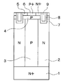
以下、本発明の第1実施形態について図を参照して説明する。図1は、本発明の第1実施形態に係る半導体装置の概略断面図である。図1に示されるように、半導体装置には多数のNch型のMOSトランジスタが形成されている。N+型層1(本発明の第2の第1導電型層に相当する)上には、ドリフト領域としてN型層2(本発明の第1の第1導電型層に相当する)およびP型層3(本発明の第1の第2導電型層に相当する)が形成されていると共に、これらN型層2およびP型層3がN+型層1の面方向に交互に配置されたスーパージャンクション構造になっている。
(First embodiment)
Hereinafter, a first embodiment of the present invention will be described with reference to the drawings. FIG. 1 is a schematic cross-sectional view of a semiconductor device according to the first embodiment of the present invention. As shown in FIG. 1, a large number of Nch-type MOS transistors are formed in the semiconductor device. On the N + type layer 1 (corresponding to the second first conductivity type layer of the present invention), as a drift region, an N type layer 2 (corresponding to the first first conductivity type layer of the present invention) and a P type The superstructure in which the layer 3 (corresponding to the first second conductivity type layer of the present invention) is formed and the N-
また、N型層2およびP型層3の表層部にはP型チャネル層4が形成されている。さらに、このP型チャネル層4の表層部のうち、N型層2の反対側にN+型ソース層5が形成され、P型層3の反対側にP+型層6が形成されている。
A P-
そして、これらN+型ソース層5およびP型チャネル層4を貫通してN型層2に達するトレンチ7が形成され、このトレンチ7の内壁表面にゲート絶縁膜8とゲート層9とが順に形成され、これらトレンチ7、ゲート絶縁膜8、ゲート層9からなるトレンチゲート構造が構成されている。
Then, a
なお、N+型ソース層5の一部とトレンチゲート構造とが図示しない絶縁膜にて覆われている。そして、N+型ソース層5、ゲート層9に電気的に接続される図示しない電極がそれぞれ形成されている。また、N+型層1には、当該N+型層1と接するように図示しないドレイン電極が形成されている。以上が本実施形態に係る半導体装置の全体構成である。
A part of the N + type
次に、上記半導体装置の製造方法について、図を参照して説明する。図2は、図1に示される半導体装置の製造工程を示した図である。 Next, a method for manufacturing the semiconductor device will be described with reference to the drawings. FIG. 2 is a diagram showing a manufacturing process of the semiconductor device shown in FIG.
図2(a)に示す工程では、シリコン基板に不純物としてAs(ヒ素)またはSb(アンチモン)またはPhos(リン)を例えば1×1015cm−3〜1×1018cm−3のドープ量でドープしたN型基板10(本発明の第1導電型の基板に相当する)を用意する。本工程で、ドープ量の下限を1×1015cm−3としているのは、これよりも低い値とするとドープの意味がなくなってしまうからである。また、ドープ量の上限を1×1018cm−3としているのは、これ以上不純物濃度が高くなると空乏層化しなくなってしまうからである。そして、不純物をドープしたN型基板10の不純物濃度を例えば比抵抗測定の方法により測定する。
In the step shown in FIG. 2A, As (arsenic), Sb (antimony), or Phos (phosphorus) is doped in the silicon substrate as an impurity, for example, in a doping amount of 1 × 10 15 cm −3 to 1 × 10 18 cm −3. A doped N-type substrate 10 (corresponding to the first conductivity type substrate of the present invention) is prepared. The reason why the lower limit of the dope amount is set to 1 × 10 15 cm −3 in this step is that the meaning of dope is lost if the value is lower than this. Moreover, the upper limit of the doping amount is set to 1 × 10 18 cm −3 because the depletion layer is not formed when the impurity concentration is further increased. Then, the impurity concentration of the N-
図2(b)に示す工程では、N型基板10の表面に図示しない酸化膜を熱酸化若しくはCVDの方法により形成し、周知のフォトリソ工程およびエッチング工程によりトレンチ11となる部分のパターンを形成する。そして、エッチング工程としてドライエッチング若しくはウェットエッチングにより深さ10μm〜100μm、幅0.1μm〜5μmのトレンチ11を形成する。
In the step shown in FIG. 2B, an oxide film (not shown) is formed on the surface of the N-
なお、ウェットエッチングによってN型基板10にトレンチ11を形成する場合、異方性エッチングを行うために、N型基板10として(110)基板を採用すると共に、KOH(水酸化カリウム)やTMAH(水酸化テトラメチルアンモニウム)等のアルカリエッチ液を用いることが好ましい。
When the
図2(c)に示す工程では、CVD装置を用意し、当該CVD装置内にN型基板10を設置すると共に、シラン或いはジクロルシラン若しくはトリクロルシランの成長ガスにホスフィン若しくはアルシン若しくはアンチモンのドーパントガスおよびトレンチ11上部におけるエピタキシャル成長を抑制するHCLガスを流す。これにより、N型基板10のトレンチ11内にP型エピタキシャル層12を埋め込む。
In the step shown in FIG. 2C, a CVD apparatus is prepared, an N-
このとき、図2(a)に示す工程で測定したN型基板10の濃度を用いて、P型エピタキシャル層12の幅(すなわちトレンチ11の幅)とその濃度との積が、トレンチ11間のN型基板10の幅(すなわちN型層2となる領域の幅)とその濃度との積が等しくなるようにP型エピタキシャル層12の濃度を調整しつつ、P型エピタキシャル層12を形成する。このようにして、N型基板10(この後の工程によりN型層2として構成される領域)とP型エピタキシャル層12とのチャージバランスを図ることができる。
At this time, using the concentration of the N-
さらに、P型エピタキシャル層12を形成する際、段階的にN型基板10の温度を下げることなく、すなわち一定温度でトレンチ11内にP型エピタキシャル層12を埋め込む。これにより、N型基板10からP型エピタキシャル層12への不純物イオンの移動を抑制することができ、ひいては外方拡散を抑制することができる。
Further, when forming the P-
図2(d)に示す工程では、N型基板10の表面側から厚さ1μm程度CMPによる研磨若しくはドライエッチによるエッチバックにより、N型基板10の表面側を平坦化する。これにより、N型基板10の表面側にP型領域(P型エピタキシャル層12)とN型領域(N型基板10)との繰り返し部分を露出させる。
In the step shown in FIG. 2D, the surface side of the N-
図2(e)に示す工程では、周知の製造工程により半導体デバイスを形成する。具体的には、フォトリソ工程、イオン注入工程、熱拡散・アニール工程によってP型チャネル層4、N+型ソース層5、P+型層6を形成する。また、フォトリソ工程、ドライエッチング工程、熱酸化工程、ポリシリコン成膜工程によりトレンチゲート構造を形成し、さらにフォトリソ工程・エッチング工程・金属成膜工程・絶縁膜形成により図示しない電極、配線、保護膜をN型基板10の表面側に形成する。
In the step shown in FIG. 2E, a semiconductor device is formed by a well-known manufacturing process. Specifically, the P-
本実施形態では、N型基板10にトレンチゲート構造が形成されることで、Nch型のMOSトランジスタが形成される。こうしてデバイスが形成されると、トレンチ11内のP型エピタキシャル層12は図1に示されるP型層3として構成される。
In the present embodiment, an Nch type MOS transistor is formed by forming a trench gate structure in the
図2(f)に示す工程では、N型基板10の裏面側を削ることでN型基板10を30μm〜120μmの厚さに薄膜化し、リンのイオン注入・拡散によりN+型層1を形成する。これにより、P型層3に挟まれたN型基板10の領域がN型層2として構成される。そして、N+型層1上に図示しないドレイン電極を形成する。
In the step shown in FIG. 2F, the N-
この後、図2(f)に示す工程を終えた基板をダイシングカットすることでチップ状に分割する。こうして図1に示される半導体装置が完成する。 Thereafter, the substrate after the process shown in FIG. 2F is diced and divided into chips. Thus, the semiconductor device shown in FIG. 1 is completed.
以上説明したように、本実施形態では、スーパージャンクション構造を構成するN型層2をN型基板10として用意し、このN型基板10を用いてスーパージャンクション構造を形成し、最後にN+型層1を形成することが特徴となっている。このように、N型層2となるエピタキシャル層を形成するのではなく、あらかじめN型の基板を用いることで、N型層2を形成するためのエピタキシャル層の形成を不要とすることができる。したがって、N型層2をエピタキシャル層として成膜する工程を無くすことができ、製造時間の短縮および製造コストの削減を実現することができる。
As described above, in the present embodiment, the N-
本実施形態のようにN+型層1をイオン注入および熱拡散にて形成する方法は、N+型の基板の上にN型のエピタキシャル層を形成する従来の方法と比較して、工程数やそれに伴う工程コストを削減することができ、製造コストを安くすることができる。
The method of forming the N +
また、N+型層1に対して濃度の低いN型基板10を用いるため、図2(c)に示す工程においてトレンチ11内にP型エピタキシャル層12を形成する際、N型基板10から形成中のP型エピタキシャル層12への不純物イオンの移動、すなわち外方拡散を抑制することができる。これにより、P型層3およびN型層2の各層におけるチャージバランスを容易に合わせることができ、ひいては半導体装置における耐圧特性を向上させることができる。
Further, since the N-
(第2実施形態)
本実施形態では、第1実施形態と異なる部分についてのみ説明する。本実施形態では、N型基板10にデバイスを形成した後、スーパージャンクション構造を形成することが特徴となっている。
(Second Embodiment)
In the present embodiment, only different parts from the first embodiment will be described. The present embodiment is characterized in that after a device is formed on the N-
図3は、本実施形態に係る半導体装置の概略断面図である。本実施形態では、第1実施形態において図1に示された半導体装置に対し、P型層においてP型チャネル層4が存在しない構成となっている。すなわち、N型層2の表層部にP型チャネル層4が形成され、このP型チャネル層4の表層部にN+型ソース層5が形成されている。そして、これらN+型ソース層5およびP型チャネル層4を貫通してN型層2に達するトレンチ7が形成され、このトレンチ7の内壁表面にゲート絶縁膜8、ゲート層9が順に形成されることでトレンチゲート構造が構成されている。また、P型層3の表層部にはP+型層6が形成されている。以上が、本実施形態に係る半導体装置の構成である。
FIG. 3 is a schematic cross-sectional view of the semiconductor device according to the present embodiment. In the present embodiment, the P-
次に、本実施形態に係る半導体装置の製造方法について、図を参照して説明する。図4は、図3に示される半導体装置の製造工程を示した図である。 Next, a method for manufacturing the semiconductor device according to the present embodiment will be described with reference to the drawings. FIG. 4 is a diagram showing a manufacturing process of the semiconductor device shown in FIG.
本実施形態では、まず、図2(a)に示す工程を終えた後、図4(a)に示す工程では、デバイスのトレンチゲート構造を形成する。すなわち、フォトリソ工程、イオン注入工程、熱拡散・アニール工程にてP型チャネル層4、N+型ソース層5を形成し、さらにフォトリソ工程、ドライエッチング工程、熱酸化工程、ポリシリコン成膜工程にてトレンチゲート構造を形成する。
In the present embodiment, first, after the process shown in FIG. 2A is finished, in the process shown in FIG. 4A, the trench gate structure of the device is formed. That is, the P-
そして、図4(b)に示す工程では、N型基板10の表面側に図示しない酸化膜を熱酸化若しくはCVDにより形成し、フォトリソ工程・エッチング工程によりトレンチ11となる部分のパターンを形成する。このとき、トレンチ11が各素子のトレンチゲート構造の間に位置するように、酸化膜をパターニングする。そして、エッチング工程としてドライエッチング若しくはウェットエッチングにより深さ10μm〜100μm、幅0.1μm〜5μmのトレンチ11を形成する。
In the step shown in FIG. 4B, an oxide film (not shown) is formed on the surface side of the N-
図4(c)に示す工程では、図2(c)に示す工程と同様にしてトレンチ11内にP型エピタキシャル層12を埋め込む。
In the step shown in FIG. 4C, the P-
図4(d)に示す工程では、図2(d)に示す工程と同様にしてN型基板10の表面側を平坦化する。さらに、フォトリソ工程・エッチング工程・金属成膜工程・絶縁膜形成によりMOSトランジスタの図示しない電極、配線、保護膜をN型基板10の表面側に形成する。
In the step shown in FIG. 4D, the surface side of the N-
図4(e)に示す工程では、図2(f)に示す工程と同様に、N+型層1を形成する。また、P型層3の表層部にP+型層6を形成する。以上のようにして、図3に示される半導体装置が完成する。
In the step shown in FIG. 4E, the N +
以上説明したように、本実施形態では、先にデバイスを形成した後、P型層3となるP型エピタキシャル層12を形成するようにしている。このように、デバイス形成後にP型エピタキシャル層12を形成しているため、繰り返しPN層(すなわちP型層3およびN型層2の繰り返し構造)に係る熱処理を低減できる。そのため、繰り返しPN層の濃度を高く維持することが可能であり、オン抵抗をより低くすることができる。
As described above, in this embodiment, after the device is formed first, the P-
(第3実施形態)
本実施形態では、上記各実施形態と異なる部分についてのみ説明する。本実施形態では、トレンチ11内に完全にP型層3を埋め込むのではなく、トレンチ11の壁面にP型エピタキシャル層12を形成した状態でトレンチ11の形状を承継したP型エピタキシャル層12内に絶縁層を埋め込むことでP型エピタキシャル層12によって構成されるP型層3とN型層2との繰り返し構造を構成することが特徴となっている。
(Third embodiment)
In the present embodiment, only different portions from the above embodiments will be described. In the present embodiment, the P-
図5は、本実施形態に係る半導体装置の概略断面図である。この図に示されるように、本実施形態では、トレンチゲート構造が形成された各N型層2に設けられたトレンチ11の内壁表面に酸化膜13とP型層3とが順に形成されている。酸化膜13としては、例えばSiO2膜が採用される。
FIG. 5 is a schematic cross-sectional view of the semiconductor device according to the present embodiment. As shown in this figure, in this embodiment, the
次に、上記半導体装置の製造方法について、図を参照して説明する。図6は、図5に示される半導体装置の製造工程を示した図である。まず、図2(a)、(b)に示す工程を行い、トレンチ11が形成されたN型基板10を用意する。なお、本実施形態においても、N型基板10の不純物濃度を測定しておく。
Next, a method for manufacturing the semiconductor device will be described with reference to the drawings. FIG. 6 is a diagram showing a manufacturing process of the semiconductor device shown in FIG. First, the steps shown in FIGS. 2A and 2B are performed to prepare the N-
そして、図6(a)に示す工程では、CVD装置を用意し、トレンチ11が形成されたN型基板10を当該CVD装置内に設置すると共に、シラン或いはジクロルシラン若しくはトリクロルシランの成長ガスにジボランのドーパントガスを流す。これにより、N型基板10のトレンチ11の壁面にP型エピタキシャル層12を成膜する。このとき、トレンチ11にトレンチ幅の半分以下の厚さでP型エピタキシャル層12を成膜する。これにより、酸化膜13を埋め込む幅を確保できる。
In the step shown in FIG. 6A, a CVD apparatus is prepared, and the N-
また、P型エピタキシャル層12を形成する際、P型エピタキシャル層12の不純物濃度がN型基板10の不純物濃度よりも高くなるようにP型エピタキシャル層12を形成する。言い換えると、(P型エピタキシャル層12の幅×P型エピタキシャル層12の不純物濃度)>(N型基板10のうちN型層2となる部分の幅×上記工程で測定したN型基板10の不純物濃度)を満たすように、P型エピタキシャル層12を形成する。
Further, when forming the P-
さらに、上記CVD装置を用いてP型エピタキシャル層12内に酸化膜13を埋め込む。この酸化膜13を埋め込む工程では、低温で行うことができるため、P型エピタキシャル層12上に容易に酸化膜13を形成できる。
Further, the
この後、図6(b)に示す工程では、N型基板10の表面側であってP型エピタキシャル層12上に形成された酸化膜13をドライエッチングにより除去すると共に、表面のP型エピタキシャル層12をドライエッチング若しくはCMPによる研磨で平坦化する。
6B, the
図6(c)に示す工程では、図2(e)に示す工程と同様にN型基板10にデバイスを形成する。こうしてデバイスが形成されると、トレンチ11内のP型エピタキシャル層12は図5に示されるP型層3として構成される。
In the step shown in FIG. 6C, a device is formed on the N-
本工程にてデバイス形成に際し、トレンチゲート構造までを形成する。そして、当該デバイスの耐圧を測定する。本実施形態では、例えばプローブをデバイスの電極部分に押し当て、ソース−ドレイン間に電圧を印加することで耐圧測定を行う。 At the time of device formation in this step, the trench gate structure is formed. Then, the breakdown voltage of the device is measured. In the present embodiment, for example, the withstand voltage is measured by pressing the probe against the electrode portion of the device and applying a voltage between the source and the drain.
このようにして測定した耐圧の値が想定した値(基準値)よりも低い場合、酸化膜13とN型基板10としてのシリコンにおけるボロンの偏析係数の違いを利用して、N+型基板を熱処理することにより、酸化膜13からP型層3のボロンを吸い出させ、P型層3の濃度を低下させる。これにより、チャージバランスを調整することができ、デバイスの耐圧を狙い値に調整することができる。
When the withstand voltage value thus measured is lower than the assumed value (reference value), the N + type substrate is heat-treated by utilizing the difference in the segregation coefficient of boron in the
したがって、本工程においてP型層3の不純物イオンを酸化膜13に吸い出させてチャーバランス調整を容易にするために、上記図6(a)に示す工程においてあらかじめP型エピタキシャル層12の不純物濃度を高めにしておくことが好ましい。
Therefore, in order to facilitate the char balance adjustment by sucking the impurity ions of the P-
また、チャージバランスを調整した後、本工程においてデバイスの図示しない電極、配線、保護膜をN型基板10の表面側に形成する。なお、耐圧測定を行い、デバイスの耐圧として狙い値が得られた場合、熱処理を行う必要はないため、デバイスの電極等を形成した後、次の工程に進む。
In addition, after adjusting the charge balance, electrodes, wirings, and protective films (not shown) of the device are formed on the surface side of the N-
そして、図6(d)に示す工程では、図2(f)に示す工程と同様にN+型層1を形成する。こうして、図5に示される半導体装置が完成する。
In the step shown in FIG. 6D, the N +
以上説明したように、本実施形態では、P型エピタキシャル層12を形成する際、トレンチ11の幅の半分以下の厚さでP型エピタキシャル層12を形成することが特徴となっている。これにより、P型層3の幅を小さくすることができ、これに伴ってP型層3の不純物濃度をN型基板10よりも高く設定することができる。また、P型層3の幅を小さくできるため、デバイスのオン抵抗を低減することができる。
As described above, the present embodiment is characterized in that when the P-
また、P型エピタキシャル層12の不純物濃度をあらかじめN型基板10よりも高くなるように形成することで、デバイス形成後にP型エピタキシャル層12の不純物イオンを酸化膜13に吸い出させ、チャージバランスを調整するようにすることができる。これにより、デバイスの耐圧を高歩留まりに保つことができる。
Further, by forming the impurity concentration of the P-
本実施形態では、上記各実施形態と同様に、半導体装置を製造するための基板としてN型基板10を用いているため、上述のように、エピタキシャル層の製造工程や製造コストを削減することができる。
In the present embodiment, the N-
(第4実施形態)
本実施形態では、上記各実施形態と異なる部分についてのみ説明する。本実施形態では、図5に示される半導体装置を製造する上で、先にデバイスを形成した後、スーパージャンクション構造を形成することが特徴となっている。
(Fourth embodiment)
In the present embodiment, only different portions from the above embodiments will be described. In the present embodiment, in manufacturing the semiconductor device shown in FIG. 5, a device is formed first, and then a super junction structure is formed.
図7は、図5に示される半導体装置の製造工程を示した図である。まず、図4(b)に示す工程までを行い、デバイスが形成されたN型基板10にトレンチ11を形成したものを用意する。なお、本実施形態においても、N型基板10の不純物濃度を測定しておく。
FIG. 7 is a diagram showing a manufacturing process of the semiconductor device shown in FIG. First, the process up to the step shown in FIG. 4B is performed to prepare a device in which the
図7(a)に示す工程では、N型基板10の表面側のうちデバイスが形成された部分(トレンチ11の開口部を除いた部分)に酸化膜14を形成し、この後、図6(a)に示す工程と同様にしてP型エピタキシャル層12および酸化膜13を形成する。
In the step shown in FIG. 7A, an
図7(b)に示す工程では、例えば図6(b)に示す工程と同様に、N型基板10の表面側に形成された酸化膜13、P型エピタキシャル層12、そして酸化膜14を除去し、N型基板10の表面側を平坦化する。そして、上記第3実施形態と同様に、デバイスの耐圧を測定し、耐圧が狙い値から外れていた場合にはN型基板10を熱処理することでチャージバランスを図る。
In the step shown in FIG. 7B, for example, as in the step shown in FIG. 6B, the
図7(c)に示す工程では、P型層3の表層部にP+型層6を形成する。また、図2(f)に示す工程と同様にN+型層1を形成する。この後、図示しない電極等を形成することで、図5に示す半導体装置が完成する。
In the step shown in FIG. 7C, the P +
以上説明したように、N型基板10に先にデバイスを形成した後、N型基板10にトレンチ11を形成してP型エピタキシャル層12および酸化膜13を形成することでスーパージャンクション構造を形成するようにしても構わない。
As described above, after a device is formed on the N-
(第5実施形態)
本実施形態では、上記各実施形態と異なる部分についてのみ説明する。本実施形態では、あらかじめ低濃度N−−型基板若しくは真性半導体基板を用いることが特徴となっている。
(Fifth embodiment)
In the present embodiment, only different portions from the above embodiments will be described. This embodiment is characterized in that a low-concentration N− type substrate or an intrinsic semiconductor substrate is used in advance.
図8は、本実施形態に係る半導体装置の概略構成図である。この図に示されるように、N+型層1上に、N−−型層15(本発明の第1導電型の基板に相当する)が形成されている。このN−−型層15は半導体装置の外縁部分にも配置されており、チップの終端部の耐圧を確保する役割を果たす。
FIG. 8 is a schematic configuration diagram of the semiconductor device according to the present embodiment. As shown in this figure, an N−− type layer 15 (corresponding to the first conductivity type substrate of the present invention) is formed on the N +
また、N−−型層15には複数のトレンチ11が形成されており、このトレンチ11の壁面にN型層16が形成され、さらにトレンチ11内のN型層16を埋めるようにP型層17が形成されている。すなわち、これらN型層16およびP型層17が繰り返し配置されることでスーパージャンクション構造が構成されている。
A plurality of
また、上記N−−型層15、N型層16、およびP型層17の表層部にはデバイスが形成されている。具体的には、N−−型層15、N型層16、P型層17の表層部にP型チャネル層4が形成されており、このP型チャネル層4の表層部にN+型ソース層5が形成されている。
Further, devices are formed on the surface layer portions of the N−−
そして、これらN+型ソース層5およびP型チャネル層4を貫通してN型層16およびN−−型層15に達するトレンチ7が形成され、このトレンチ7の内壁表面にゲート絶縁膜8とゲート層9とが順に形成され、これらトレンチ7、ゲート絶縁膜8、ゲート層9からなるトレンチゲート構造が構成されている。
A
さらに、P型層17上に形成されたP型チャネル層4上にP+型層6が形成されている。なお、上記各実施形態と同様に、トレンチゲート構造の上部にはゲート電極やソース電極等の電極、配線、絶縁膜等が形成されている。また、N−−型層15には、当該N−−型層15と接するように図示しないドレイン電極が形成されている。以上が、本実施形態に係る半導体装置の全体構成である。
Further, a P +
次に、上記半導体装置の製造方法について、図を参照して説明する。図9は、図8に示される半導体装置の製造工程を示した図である。 Next, a method for manufacturing the semiconductor device will be described with reference to the drawings. FIG. 9 is a diagram showing a manufacturing process of the semiconductor device shown in FIG.
図9(a)に示す工程では、シリコン基板に不純物としてAsまたはSbまたはPhosを1×1015cm−3以下の濃度でドープした低濃度N−−型基板18を用意する。なお、真性半導体基板であっても構わない。また、図9(b)に示す工程では、図2(b)に示す工程と同様にトレンチ11を形成する。
In the step shown in FIG. 9A, a low-concentration N−
図9(c)に示す工程では、トレンチ11の側面および底部に気相拡散若しくはイオン注入によりホスフィン若しくはアルシン、若しくはアンチモンをドープすることで、N型層16を形成する。
In the step shown in FIG. 9C, the N-
さらに、CVD装置を用意し、N型層16が形成されたN−−型基板18を当該CVD装置内に設置すると共に、シラン或いはジクロルシラン若しくはトリクロルシランの成長ガスにジボランのドーパントガスおよびトレンチ11上部のエピタキシャル成長を抑制するHCLガスを流してN型層16内にP型エピタキシャル層12を埋め込む。
Further, a CVD apparatus is prepared, and an N−−
図9(d)に示す工程では、図2(d)に示す工程と同様に、同様にしてN−−型基板18の表面側を平坦化する。これにより、これにより、N−−型基板18の表面側にP型領域(P型エピタキシャル層12)とN型領域(N型層16)との繰り返し部分を露出させる。
In the step shown in FIG. 9D, the surface side of the N−−
図9(e)に示す工程では、図2(e)に示す工程と同様の方法でデバイスを形成する。こうしてデバイスが形成されると、トレンチ11内のP型エピタキシャル層12は図8に示されるP型層17として構成される。
In the step shown in FIG. 9E, a device is formed by the same method as the step shown in FIG. When the device is thus formed, the P-
図9(f)に示す工程では、図2(f)に示す工程と同様に、N+型層1を形成する。このとき、トレンチ11の底面に形成されたN型層16もN+型層1とされる。この後、上記各実施形態と同様にデバイスの電極等を形成することにより、図8に示される半導体装置が完成する。
In the step shown in FIG. 9F, the N +
以上説明したように、本実施形態では、チップとして構成される半導体装置の終端部の耐圧を考慮して、あらかじめ低濃度N−−型基板18(または真性半導体基板)を用いて半導体装置を製造することが特徴となっている。また、このN−−型基板18にトレンチ11を形成し、このトレンチ11内にスーパージャンクション構造を構成している。これにより、半導体装置を製造するに際し、基板としてスーパージャンクション構造の一部となる層をエピタキシャル層として成膜する必要はなく、製造工程数や製造コストを削減することができる。
As described above, in the present embodiment, a semiconductor device is manufactured using a low-concentration N−− type substrate 18 (or an intrinsic semiconductor substrate) in advance in consideration of the breakdown voltage of the terminal portion of the semiconductor device configured as a chip. It is characterized by. Further, a
また、トレンチ11の側面および底部に気相拡散若しくはイオン注入によりN型層16を形成するようにしているため、このN型層16の幅を小さくすることができ、デバイスのオン抵抗を低減することができる。
In addition, since the N-
さらに、本実施形態では、あらかじめ低濃度N−−型基板18を用いているため、チップ状の半導体装置の終端部の耐圧を考慮したものを製造することができる。
Furthermore, in the present embodiment, since the low concentration N−
(第6実施形態)
本実施形態では、上記各実施形態と異なる部分についてのみ説明する。本実施形態では、上記第3実施形態と第5実施形態とを組み合わせたことが特徴となっている。
(Sixth embodiment)
In the present embodiment, only different portions from the above embodiments will be described. The present embodiment is characterized in that the third embodiment and the fifth embodiment are combined.
図10は、本実施形態に係る半導体装置の概略断面図である。この図に示されるように、本実施形態では、トレンチ11の壁面にN型層16が形成されている。そして、このN型層16の壁面にP型層17が形成されており、このP型層17内に酸化膜13が形成された構造になっている。
FIG. 10 is a schematic cross-sectional view of the semiconductor device according to the present embodiment. As shown in this figure, in this embodiment, an N-
次に、上記半導体装置の製造方法について、図を参照して説明する。図11は、図10に示される半導体装置の製造工程を示した図である。まず、図9(a)、(b)に示す工程を行い、トレンチ11が形成されたN−−型基板18を用意する。
Next, a method for manufacturing the semiconductor device will be described with reference to the drawings. FIG. 11 shows a manufacturing process of the semiconductor device shown in FIG. First, the steps shown in FIGS. 9A and 9B are performed to prepare an N−−
図11(a)に示す工程では、トレンチ11の側面および底部に気相拡散若しくはイオン注入によりホスフィン若しくはアルシン、若しくはアンチモンをドープすることで、N型層16を形成する。
In the step shown in FIG. 11A, the side surface and bottom of the
また、CVD装置を用意し、当該CVD装置内にN型層16が形成されたN−−型基板18を設置すると共に、シラン或いはジクロルシラン若しくはトリクロルシランの成長ガスにジボランのドーパントガスを流してN型層16が完全に埋まらないようにN型層16の壁面にP型エピタキシャル層12を成膜する。さらに、当該CVD装置を用いてP型エピタキシャル層12内に酸化膜13を埋め込む。
Also, a CVD apparatus is prepared, an N-
図11(b)に示す工程では、N−−型基板18の表面に形成されたN型層16、P型エピタキシャル層12、酸化膜13のうち、まず酸化膜13をドライエッチで除去すると共に、さらにP型エピタキシャル層12、N型層16をドライエッチ若しくはCMPによる研磨で平坦化する。これにより、N−−型基板18の表面にP型領域(P型エピタキシャル層12)およびN型領域(N型層16)の繰り返し部分を露出させる。
In the step shown in FIG. 11B, among the N-
図11(c)に示す工程では、図6(c)と同様にデバイスを形成する。そして、トレンチ11内のP型エピタキシャル層12は図10に示されるP型層3として構成される。
In the step shown in FIG. 11C, a device is formed in the same manner as in FIG. The P-
図11(d)に示す工程では、図9(f)に示す工程と同様にN+型層1を形成する。この後、上述のように、図示しない電極等を形成することで、図10に示される半導体装置が完成する。
In the step shown in FIG. 11D, the N +
以上説明したように、N−−型基板18に設けたトレンチ11内にP型層17、そして酸化膜13を形成するようにしても構わない。
As described above, the P-
(第7実施形態)
本実施形態では、上記各実施形態と異なる部分についてのみ説明する。本実施形態では、上記各実施形態で示したNch型のMOSトランジスタと、Pch型のMOSトランジスタとを1つのチップに形成したことが特徴となっている。
(Seventh embodiment)
In the present embodiment, only different portions from the above embodiments will be described. The present embodiment is characterized in that the Nch-type MOS transistor and the Pch-type MOS transistor shown in the above embodiments are formed on one chip.
図12は、本実施形態に係る半導体装置の概略断面図である。この図に示されるように、N型層2およびP型層3が繰り返し配置されたスーパージャンクション構造が形成されている。また、図12に示される半導体装置にはNch型のMOSトランジスタとPch型のMOSトランジスタとが形成されている。
FIG. 12 is a schematic cross-sectional view of the semiconductor device according to the present embodiment. As shown in this figure, a super junction structure is formed in which an N-
半導体装置において、Nch型のMOSトランジスタが形成された領域では、N型領域にトレンチゲート構造が形成されており、基板において当該トレンチゲート構造の反対側にN+型層1が形成されている。また、半導体装置において、Pch型のMOSトランジスタが形成された領域では、P型領域にトレンチゲート構造が形成されており、基板において当該トレンチゲート構造の反対側にP+型層19(本発明の第2の第2導電型層に相当する)が形成されている。
In a semiconductor device, in a region where an Nch type MOS transistor is formed, a trench gate structure is formed in the N type region, and an N +
本実施形態では、周知のフォトリソ工程等により、基板の裏面側にN+型層1およびP+型層19を選択的に形成することができる。なお、P+型層19を形成する場合、ボロンをイオン注入して拡散することとなる。
In this embodiment, the N +
以上のように、N型層2およびP型層3が繰り返し配置されたスーパージャンクション構造を有する半導体装置において、Nch型およびPch型の各のMOSトランジスタを形成したものとすることができる。
As described above, in a semiconductor device having a super junction structure in which the N-
(他の実施形態)
上記第1〜第6実施形態では、デバイスとしてNch型のMOSトランジスタを備えた半導体装置について説明したが、P型層3にトレンチゲート構造を形成することにより、デバイスとしてPch型のMOSトランジスタを備えた半導体装置を製造することもできる。
(Other embodiments)
In the first to sixth embodiments, the semiconductor device including the Nch type MOS transistor as the device has been described. However, by forming a trench gate structure in the
また、上記第1〜第6実施形態では、半導体装置を製造する際にN型基板10を用いているが、P型基板を用いて半導体装置を製造するようにしても構わない。すなわち、上記第1〜第6実施形態において、半導体装置をN型とP型を入れ替えたものとすることもできる。例えば、第1〜第4実施形態では、N型基板10の代わりにP型基板を用意し、第5、第6実施形態では、N−−型基板18の代わりにP−−型基板を用意し、それぞれ各基板に半導体装置を製造することとなる。
In the first to sixth embodiments, the N-
第1実施形態において、図1に示される半導体装置では、N+型層1上にP型層3およびN型層2が形成された構造になっているが、図2(f)に示す工程においてN型基板10を削る量を調整することで、N+型層1とP型層3との間にN型層2が挟まれた構造になっていても構わない。
In the first embodiment, the semiconductor device shown in FIG. 1 has a structure in which a P-
第3実施形態において、図5に示される半導体装置では、N+型層1とP型層3との間に酸化膜13が形成された構造になっているが、図6(d)に示す工程においてN型基板10を削る量を調整することで、N+型層1上にP型層3が形成された構造になっていても構わない。
In the third embodiment, the semiconductor device shown in FIG. 5 has a structure in which the
上記第3実施形態では、図6(c)に示す工程において、P型エピタキシャル層12をCVD装置により成膜しているが、P型エピタキシャル層12を成膜する代わりに、気相拡散若しくはイオン注入でトレンチ11の側壁にドーピングを行ってP型エピタキシャル層12に相当するP型層を形成すると共に、このP型層内に酸化膜13を埋め込むようにすることもできる。
In the third embodiment, in the step shown in FIG. 6C, the P-
また、第3、第4実施形態では、N型基板10のトレンチ11壁面にP型層3をエピタキシャル成長させて形成しているが、トレンチ11の側壁から気相拡散若しくはイオン注入によりP型層3を形成するようにしても構わない。この場合においても、デバイス形成後に酸化膜13にP型層3の不純物イオンを吸い出させてチャージバランスを図ることができるようにするため、気相拡散若しくはイオン注入の際に、トレンチ11内に形成したP型層3の不純物濃度がN型基板10の不純物濃度よりも高くなるようにP型層3を形成することが好ましい。
In the third and fourth embodiments, the P-
上記第5、第6実施形態においては、第2、第4実施形態と同様に、先にN−−型基板18にデバイスを形成した後、トレンチ11を形成してN型層16およびP型層3を形成することでスーパージャンクション構造を形成することもできる。また、N−−型基板18のトレンチ11壁面に気相拡散若しくはイオン注入の方法によってN型層2を形成しているが、トレンチ11内にN型層2をエピタキシャル成長させてN型層2を形成するようにしても構わない。
In the fifth and sixth embodiments, as in the second and fourth embodiments, after the device is first formed on the N−−
第7実施形態では、Nch型およびPch型のMOSトランジスタを1つのチップに形成した半導体装置について説明したが、この半導体装置に例えば第3実施形態で示された酸化膜13を形成した構成としても良い。また、Nch型およびPch型のMOSトランジスタを1つのチップに形成する場合、第5、第6実施形態のように、チップの終端部の耐圧を考慮したものとしてN型層2を備えるようにしても良い。この場合、上述のように、N−−型基板18にトレンチを形成して繰り返し構造を形成し、第7実施形態のようにNch型およびPch型のMOSトランジスタをそれぞれ形成することとなる。
In the seventh embodiment, the semiconductor device in which the Nch-type and Pch-type MOS transistors are formed on one chip has been described. However, for example, the
1…N+型層、2…N型層、3…P型層、10…N型基板、11…トレンチ、13…酸化膜、15…N−−型層、18…N−−型基板。
DESCRIPTION OF
Claims (20)
前記繰り返し構造を構成する前記第1の第1導電型層(2)および前記第1の第2導電型層(3)のうち前記第1の第1導電型層(2)をドリフト領域とする縦型の第1導電型チャネルの半導体素子を備えた半導体装置の製造方法であって、
第1導電型の基板(10)を用意する工程と、
前記第1導電型の基板(10)の表面側にトレンチ(11)を形成する工程と、
前記トレンチ(11)内に前記第1の第2導電型層(3)を形成することで、前記第1導電型の基板(10)のうち前記各第1の第2導電型層(3)に挟まれた領域を前記第1の第1導電型層(2)とし、当該第1の第1導電型層(2)と前記第1の第2導電型層(3)とが交互に配置された前記繰り返し構造を形成する工程と、
前記繰り返し構造が形成された前記第1導電型の基板(10)の裏面側を薄膜化した後、当該裏面側に前記第1の第1導電型層(2)よりも不純物濃度が高い前記第2の第1導電型層(1)を形成する工程と、を含んでいることを特徴とする半導体装置の製造方法。 A first first conductivity type layer (2) and a first second conductivity type layer (3) as a drift region are formed on the second first conductivity type layer (1), and the first The first conductivity type layer (2) and the first second conductivity type layer (3) have a repeated structure in which the first conductivity type layer (3) is repeatedly arranged in the plane direction of the second first conductivity type layer (1),
Of the first first conductivity type layer (2) and the first second conductivity type layer (3) constituting the repetitive structure, the first first conductivity type layer (2) is used as a drift region. a method of manufacturing a vertical semiconductor device having a semiconductor device of a first conductivity type channel,
Preparing a first conductivity type substrate (10);
Forming a trench (11) on the surface side of the first conductivity type substrate (10);
The first second conductivity type layer (3) of the first conductivity type substrate (10) is formed by forming the first second conductivity type layer (3) in the trench (11). The region sandwiched between the first conductive type layers (2) is alternately arranged with the first first conductive type layers (2) and the first second conductive type layers (3). Forming the repeated structure,
After thinning the back surface side of the first conductivity type substrate (10) on which the repetitive structure is formed, the impurity concentration higher than that of the first first conductivity type layer (2) is formed on the back surface side. Forming a second first conductivity type layer (1). 2. A method of manufacturing a semiconductor device, comprising:
前記繰り返し構造を構成する前記第1の第1導電型層(2)および前記第1の第2導電型層(3)のうち前記第1の第1導電型層(2)をドリフト領域とする縦型の第1導電型チャネルの半導体素子と前記第1の第2導電型層(3)をドリフト領域とする縦型の第2導電型チャネルの半導体素子とを備えた半導体装置の製造方法であって、
第1導電型の基板(10)を用意する工程と、
前記第1導電型の基板(10)の表面側にトレンチ(11)を形成する工程と、
前記トレンチ(11)内に前記第1の第2導電型層(3)を形成することで、前記第1導電型の基板(10)のうち前記各第1の第2導電型層(3)に挟まれた領域を前記第1の第1導電型層(2)とし、当該第1の第1導電型層(2)と前記第1の第2導電型層(3)とが交互に配置された前記繰り返し構造を形成する工程と、
前記第1導電型の基板(10)の裏面側において前記繰り返し構造のうち前記縦型の第1導電型チャネルの半導体素子が形成された領域に前記第1の第1導電型層(2)よりも不純物濃度が高い前記第2の第1導電型層(1)を形成し、前記繰り返し構造のうち前記縦型の第2導電型チャネルの半導体素子が形成された領域に前記第1の第2導電型層(3)よりも不純物濃度が高い前記第2の第2導電型層(19)を形成する工程と、を含んでいることを特徴とする半導体装置の製造方法。 The first first conductivity type layer (2) and the first second conductivity type layer (3) as the drift region are on the second first conductivity type layer (1) or the second first conductivity type layer. (1) formed on the second second conductivity type layer (19) adjacent in the plane direction, and the first first conductivity type layer (2) and the first second conductivity type layer. (3) has a repeating structure in which the second first conductivity type layer (1) or the second second conductivity type layer (19) is repeatedly arranged in the plane direction;
Of the first first conductivity type layer (2) and the first second conductivity type layer (3) constituting the repetitive structure, the first first conductivity type layer (2) is used as a drift region. in method for manufacturing the vertical semiconductor device including a semiconductor element of the vertical of the second conductivity type channel said first conductivity type channel semiconductor device of the first second-conductivity type layer (3) and a drift region of There,
Preparing a first conductivity type substrate (10);
Forming a trench (11) on the surface side of the first conductivity type substrate (10) ;
By forming the pre-Symbol trenches (11) said first second-conductivity-type layer in (3), wherein each of the first second conductivity type layer of the first conductivity type substrate (10) (3 ) Is the first first conductivity type layer (2), and the first first conductivity type layer (2) and the first second conductivity type layer (3) are alternately arranged. Forming the arranged repetitive structure; and
From the first first conductivity type layer (2) in the region where the semiconductor element of the vertical first conductivity type channel is formed in the repetitive structure on the back surface side of the first conductivity type substrate (10). The second first-conductivity-type layer (1) having a high impurity concentration is formed, and the first second-conductivity layer is formed in a region where the semiconductor element of the vertical second-conductivity-type channel is formed in the repetitive structure. Forming a second second conductivity type layer (19) having an impurity concentration higher than that of the conductivity type layer (3).
前記第1の第2導電型層(3)を形成する工程では、前記不純物濃度を測定する工程で得られた前記第1導電型の基板(10)の不純物濃度とトレンチ幅を測定する工程で得られた前記各第1の第2導電型層(3)の間の前記第1の第1導電型層(2)の幅との積が、前記各第1の第1導電型層(2)の間の前記第1の第2導電型層(3)の幅と当該第1の第2導電型層(3)の不純物濃度の積に等しくなるように、前記第1の第2導電型層(3)の不純物濃度を調整しつつ当該第1の第2導電型層(3)を形成することを特徴とする請求項1または2に記載の半導体装置の製造方法。 The step of preparing the first conductivity type substrate (10) includes the step of measuring the impurity concentration of the first conductivity type substrate (10) and the step of measuring the trench width.
In the step of forming the first second conductivity type layer (3), the step of measuring the impurity concentration and trench width of the substrate (10) of the first conductivity type obtained in the step of measuring the impurity concentration. The product of the width of the first first conductivity type layer (2) between the obtained first second conductivity type layers (3) is the first first conductivity type layer (2 ) Between the width of the first second conductivity type layer (3) and the impurity concentration of the first second conductivity type layer (3). The method for manufacturing a semiconductor device according to claim 1, wherein the first second conductivity type layer (3) is formed while adjusting an impurity concentration of the layer (3).
前記トレンチ(11)を形成する工程では、前記第1導電型の基板(10)のうち前記各縦型の第1導電型チャネルの半導体素子の間に前記トレンチ(11)を形成することを特徴とする請求項1ないし4のいずれか1つに記載の半導体装置の製造方法。 In the step of preparing the first conductivity type substrate (10), after the first conductivity type substrate (10) is prepared, the vertical type first substrate is formed on a surface layer portion of the first conductivity type substrate (10) . It includes a step of forming a semiconductor device of the first conductivity type channel,
In the step of forming the trench (11), the trench (11) is formed between the semiconductor elements of the vertical first conductivity type channels in the first conductivity type substrate (10). A method for manufacturing a semiconductor device according to claim 1.
当該繰り返し構造を挟むように前記第2の第1導電型層(1)の面方向に酸化膜(13)が配置され、前記繰り返し構造を構成する前記第1の第1導電型層(2)および前記第1の第2導電型層(3)のうち前記第1の第1導電型層(2)をドリフト領域とする縦型の第1導電型チャネルの半導体素子を備えた半導体装置の製造方法であって、
第1導電型の基板(10)を用意する工程と、
前記第1導電型の基板(10)の表面側にトレンチ(11)を形成する工程と、
前記トレンチ(11)の内壁面に当該トレンチ(11)の幅の半分以下の厚さで前記第1の第2導電型層(3)をエピタキシャル成膜する工程と、
前記第1の第2導電型層(3)上に前記酸化膜(13)を形成して当該酸化膜(13)で前記トレンチ(11)を埋めることで、前記第1導電型の基板(10)のうち前記各第1の第2導電型層(3)に挟まれた領域を前記第1の第1導電型層(2)とし、当該第1の第1導電型層(2)と前記第1の第2導電型層(3)とが交互に配置された前記繰り返し構造を形成する工程と、
前記繰り返し構造が形成された前記第1導電型の基板(10)の裏面側を薄膜化した後、当該裏面側に前記第1の第1導電型層(2)よりも不純物濃度が高い前記第2の第1導電型層(1)を形成する工程と、を含んでいることを特徴とする半導体装置の製造方法。 A first first conductivity type layer (2) and a first second conductivity type layer (3) as a drift region are formed on the second first conductivity type layer (1), and the first The first conductivity type layer (2) and the first second conductivity type layer (3) have a repeated structure in which the first conductivity type layer (3) is repeatedly arranged in the plane direction of the second first conductivity type layer (1),
An oxide film (13) is arranged in the surface direction of the second first conductivity type layer (1) so as to sandwich the repeated structure, and the first first conductivity type layer (2) constituting the repeat structure. and manufacturing a semiconductor device having a semiconductor element of a vertical-type first conductivity type channel of said first first-conductivity type layer (2) a drift region of the first second-conductivity type layer (3) A method,
Preparing a first conductivity type substrate (10);
Forming a trench (11) on the surface side of the first conductivity type substrate (10);
Epitaxially forming the first second-conductivity-type layer (3) on the inner wall surface of the trench (11) with a thickness less than half the width of the trench (11);
The oxide film (13) is formed on the first second conductivity type layer (3), and the trench (11) is filled with the oxide film (13), whereby the first conductivity type substrate (10) is formed. ), The region sandwiched between the first second conductivity type layers (3) is the first first conductivity type layer (2), and the first first conductivity type layer (2) and the Forming the repetitive structure in which the first second conductivity type layers (3) are alternately arranged;
After thinning the back surface side of the first conductivity type substrate (10) on which the repetitive structure is formed, the impurity concentration higher than that of the first first conductivity type layer (2) is formed on the back surface side. Forming a second first conductivity type layer (1). 2. A method of manufacturing a semiconductor device, comprising:
当該繰り返し構造を挟むように前記第2の第1導電型層(1)の面方向に酸化膜(13)が配置され、前記繰り返し構造を構成する前記第1の第1導電型層(2)および前記第1の第2導電型層(3)のうち前記第1の第1導電型層(2)をドリフト領域とする縦型の第1導電型チャネルの半導体素子を備えた半導体装置の製造方法であって、
第1導電型の基板(10)を用意する工程と、
前記第1導電型の基板(10)の表面側にトレンチ(11)を形成する工程と、
前記トレンチ(11)の内壁面を気相拡散するか若しくは前記トレンチ(11)の内壁面にイオン注入を行うことで前記トレンチ(11)の壁面を前記第1の第2導電型層(3)に形成する工程と、
前記第1の第2導電型層(3)上に酸化膜(13)を形成して当該酸化膜(13)で前記トレンチ(11)を埋めることで、前記第1導電型の基板(10)のうち前記各第1の第2導電型層(3)に挟まれた領域を前記第1の第1導電型層(2)とし、当該第1の第1導電型層(2)と前記第1の第2導電型層(3)とが交互に配置された前記繰り返し構造を形成する工程と、
前記繰り返し構造が形成された前記第1導電型の基板(10)の裏面側を薄膜化した後、当該裏面側に前記第1の第1導電型層(2)よりも不純物濃度が高い前記第2の第1導電型層(1)を形成する工程と、を含んでいることを特徴とする半導体装置の製造方法。 A first first conductivity type layer (2) and a first second conductivity type layer (3) as a drift region are formed on the second first conductivity type layer (1), and the first The first conductivity type layer (2) and the first second conductivity type layer (3) have a repeated structure in which the first conductivity type layer (3) is repeatedly arranged in the plane direction of the second first conductivity type layer (1),
An oxide film (13) is arranged in the surface direction of the second first conductivity type layer (1) so as to sandwich the repeated structure, and the first first conductivity type layer (2) constituting the repeat structure. and manufacturing a semiconductor device having a semiconductor element of a vertical-type first conductivity type channel of said first first-conductivity type layer (2) a drift region of the first second-conductivity type layer (3) A method,
Preparing a first conductivity type substrate (10);
Forming a trench (11) on the surface side of the first conductivity type substrate (10);
The inner wall surface of the trench (11) is vapor-phase diffused, or ion implantation is performed on the inner wall surface of the trench (11) to form the wall surface of the trench (11) with the first second conductivity type layer (3). Forming the step,
An oxide film (13) is formed on the first second conductivity type layer (3), and the trench (11) is filled with the oxide film (13), whereby the first conductivity type substrate (10). The region sandwiched between the first second conductivity type layers (3) is defined as the first first conductivity type layer (2), and the first first conductivity type layer (2) and the first Forming the repetitive structure in which one second conductivity type layer (3) is alternately arranged;
After thinning the back surface side of the first conductivity type substrate (10) on which the repetitive structure is formed, the impurity concentration higher than that of the first first conductivity type layer (2) is formed on the back surface side. Forming a second first conductivity type layer (1). 2. A method of manufacturing a semiconductor device, comprising:
前記トレンチ(11)を形成する工程では、前記第1導電型の基板(10)のうち前記各縦型の第1導電型チャネルの半導体素子の間に前記トレンチ(11)を形成することを特徴とする請求項7または8に記載の半導体装置の製造方法。 In the step of preparing the first conductivity type substrate (10), after the first conductivity type substrate (2) is prepared, the vertical type second substrate is formed on the surface layer portion of the first conductivity type substrate (10) . It includes a step of forming a semiconductor device of the first conductivity type channel,
In the step of forming the trench (11), the trench (11) is formed between the semiconductor elements of the vertical first conductivity type channels in the first conductivity type substrate (10). A method for manufacturing a semiconductor device according to claim 7 or 8.
前記縦型の第1導電型チャネルの半導体素子を形成する工程では、前記縦型の第1導電型チャネルの半導体素子を形成した後、当該縦型の第1導電型チャネルの半導体素子の耐圧を測定する工程を含んでおり、
当該耐圧を測定する工程では、前記耐圧が基準値よりも低い場合、前記第1導電型の基板(10)の不純物濃度と前記各第1の第2導電型層(3)の間の前記第1の第1導電型層(2)の幅との積が、前記各第1の第1導電型層(2)の間の前記第1の第2導電型層(3)の幅と当該第1の第2導電型層(3)の不純物濃度の積に等しくなるように、前記第1導電型の基板(10)を熱処理して前記第1の第2導電型層(3)から当該第1の第2導電型層(3)に含まれる不純物イオンを前記酸化膜(13)に吸い出させる工程を含んでいることを特徴とする請求項9または10に記載の半導体装置の製造方法。 The step of preparing the first conductivity type substrate (10) includes the step of measuring the impurity concentration of the first conductivity type substrate (10),
In the step of forming a semiconductor device of a first conductivity type channel of said vertical, after forming a semiconductor device of a first conductivity type channel of said vertical, the breakdown voltage of the semiconductor device of the first conductivity type channel of the vertical Including the process of measuring,
In the step of measuring the breakdown voltage, when the breakdown voltage is lower than a reference value, the impurity concentration of the first conductivity type substrate (10) and the first conductivity type layer (3) between the first second conductivity type layers (3). The product of the width of the first first conductivity type layer (2) and the width of the first second conductivity type layer (3) between the first first conductivity type layers (2) The first conductivity type substrate (10) is heat-treated so as to be equal to the product of the impurity concentration of the first second conductivity type layer (3), and the first second conductivity type layer (3) is removed from the first conductivity type layer (3). 11. The method of manufacturing a semiconductor device according to claim 9, further comprising a step of sucking out impurity ions contained in one second conductivity type layer (3) into the oxide film (13).
さらに、前記第1の第1導電型層(2)および前記第1の第2導電型層(3)が前記第2の第1導電型層(1)の面方向に繰り返し配置された繰り返し構造をなしており、
当該繰り返し構造を構成する前記第1の第1導電型層(2)および前記第1の第2導電型層(3)のうち前記第1の第1導電型層(2)と、前記各第1の第1導電型層(2)間の第3の第1導電型層(15)をドリフト領域とする縦型の第1導電型チャネルの半導体素子を備えた半導体装置の製造方法であって、
第1の第1導電型層(2)よりも不純物濃度が低い第1導電型の基板(18)を用意する工程と、
前記第1導電型の基板(18)の表面側にトレンチ(11)を形成する工程と、
前記トレンチ(11)の内壁面を気相拡散するか若しくは前記トレンチ(11)の内壁面にイオン注入を行うことで前記トレンチ(11)の壁面を前記第1の第1導電型層(2)に形成する工程と、
前記第1の第1導電型層(2)上に第1の第2導電型層(3)をエピタキシャル成膜することで、前記第1の第1導電型層(2)と前記第1の第2導電型層(3)とが交互に配置された前記繰り返し構造を形成する工程と、
前記繰り返し構造が形成された前記第1導電型の基板(18)の裏面側を薄膜化した後、当該裏面側に前記第1の第1導電型層(2)よりも不純物濃度が高い前記第2の第1導電型層(1)を形成し、前記第2の第1導電型層(1)上の外縁部に前記第1導電型の基板(18)に基づく前記第3の第1導電型層(15)を構成する工程と、を含んでいることを特徴とする半導体装置の製造方法。 The third first conductivity type layer (2) and the first second conductivity type layer (3) as the drift region have a third impurity concentration lower than that of the first first conductivity type layer (2). The first first conductivity type layer (2) is formed on the first conductivity type layer (15), and the first second conductivity type layer (15) is positioned on the outer edge portion. A conductive layer (3), the third first conductive layer (15) is formed on the second first conductive layer (1);
Furthermore, the repeating structure in which the first first conductivity type layer (2) and the first second conductivity type layer (3) are repeatedly arranged in the surface direction of the second first conductivity type layer (1). And
Of the first first conductivity type layer (2) and the first second conductivity type layer (3) constituting the repetitive structure, the first first conductivity type layer (2), A method of manufacturing a semiconductor device comprising a semiconductor element of a vertical first conductivity type channel having a third first conductivity type layer (15) between one first conductivity type layer (2) as a drift region. ,
Preparing a first conductivity type substrate (18) having an impurity concentration lower than that of the first first conductivity type layer (2);
Forming a trench (11) on the surface side of the first conductivity type substrate (18);
The inner wall surface of the trench (11) is vapor-phase diffused, or ion implantation is performed on the inner wall surface of the trench (11) to form the wall surface of the trench (11) with the first first conductivity type layer (2). Forming the step,
By epitaxially forming a first second conductivity type layer (3) on the first first conductivity type layer (2), the first first conductivity type layer (2) and the first first conductivity type layer (2) are formed. Forming the repeating structure in which two conductivity type layers (3) are alternately arranged;
After thinning the back surface side of the first conductivity type substrate (18) on which the repetitive structure is formed, the impurity concentration higher than that of the first first conductivity type layer (2) is formed on the back surface side. The second first conductivity type layer (1) is formed, and the third first conductivity based on the first conductivity type substrate (18) is formed on the outer edge of the second first conductivity type layer (1). And a step of forming a mold layer (15).
前記トレンチ(11)内では、前記第1の第1導電型層(2)および前記第1の第2導電型層(3)が前記第2の第1導電型層(1)の面方向に繰り返し配置された繰り返し構造をなしており、
さらに、前記繰り返し構造を構成する前記第1の第1導電型層(2)および前記第1の第2導電型層(3)のうち前記第1の第1導電型層(2)と、当該第1の第1導電型層(2)に挟まれた前記第3の第1導電型層(15)をドリフト領域とする縦型の第1導電型チャネルの半導体素子を備えた半導体装置の製造方法であって、
前記第1の第1導電型層(2)よりも不純物濃度が低い第1導電型の基板(18)を用意する工程と、
前記第1導電型の基板(18)の表面側に前記トレンチ(11)を形成する工程と、
前記トレンチ(11)の内壁面に前記第1の第1導電型層(2)をエピタキシャル成膜する工程と、
前記第1の第1導電型層(2)上に前記第1の第2導電型層(3)をエピタキシャル成膜することで、前記第1の第1導電型層(2)と前記第1の第2導電型層(3)とが交互に配置された前記繰り返し構造を形成する工程と、
前記繰り返し構造が形成された前記第1導電型の基板(18)の裏面側を薄膜化した後、当該裏面側に前記第1の第1導電型層(2)よりも不純物濃度が高い前記第2の第1導電型層(1)を形成し、前記第2の第1導電型層(1)上の外縁部に前記第1導電型の基板(18)に基づく前記第3の第1導電型層(15)を構成する工程と、を含んでいることを特徴とする半導体装置の製造方法。 The third first conductivity type layer (2) and the first second conductivity type layer ( 3 ) as the drift region have a third impurity concentration lower than that of the first first conductivity type layer (2). The first first conductivity type layer (15) is disposed in a trench (11) formed in the one conductivity type layer (15), and the third first conductivity type layer (15) is positioned at an outer edge. 2) the first second conductivity type layer (3) and the third first conductivity type layer (15) are formed on the second first conductivity type layer (1);
In the trench (11), the first first conductivity type layer (2) and the first second conductivity type layer (3) are arranged in the plane direction of the second first conductivity type layer (1). It has a repeated structure arranged repeatedly,
Furthermore, among the first first conductivity type layer (2) and the first second conductivity type layer (3) constituting the repetitive structure, the first first conductivity type layer (2), and manufacturing of a semiconductor device having a semiconductor element of a vertical-type first conductivity type channel of a first first-conductivity type layer (2) sandwiched by said third first-conductivity type layer (15) of the drift region A method,
Preparing a first conductivity type substrate (18) having an impurity concentration lower than that of the first first conductivity type layer (2);
Forming the trench (11) on the surface side of the first conductivity type substrate (18);
Epitaxially forming the first first conductivity type layer (2) on the inner wall surface of the trench (11);
Wherein by the first first conductivity type layer (2) said first second-conductivity type layer on the (3) epitaxially deposited, the first first conductivity type layer (2) and the first Forming the repeating structure in which the second conductivity type layers (3) are alternately arranged;
After thinning the back surface side of the first conductivity type substrate (18) on which the repetitive structure is formed, the impurity concentration higher than that of the first first conductivity type layer (2) is formed on the back surface side. The second first conductivity type layer (1) is formed, and the third first conductivity based on the first conductivity type substrate (18) is formed on the outer edge of the second first conductivity type layer (1). And a step of forming a mold layer (15).
前記各繰り返し構造の間に前記第1の第1導電型層(2)よりも不純物濃度が低い第3の第1導電型層(15)が形成され、当該第3の第1導電型層(15)を挟んだ前記各繰り返し構造が酸化膜(13)に挟まれた状態になっており、
前記第3の第1導電型層(15)が外縁部に位置するように前記繰り返し構造、前記酸化膜(13)、前記第3の第1導電型層(15)が前記第2の第1導電型層(1)上に形成され、さらに前記第1の第1導電型層(2)と、前記各第1の第1導電型層(2)の間の前記第3の第1導電型層(15)をドリフト領域とする縦型の第1導電型チャネルの半導体素子を備えた半導体装置の製造方法であって、
前記第1の第1導電型層(2)よりも不純物濃度が低い第1導電型の基板(18)を用意する工程と、
前記第1導電型の基板(18)の表面側にトレンチ(11)を形成する工程と、
前記トレンチ(11)の内壁面を気相拡散するか若しくは前記トレンチ(11)の内壁面にイオン注入を行うことで前記トレンチ(11)の壁面を前記第1の第1導電型層(2)に形成する工程と、
前記トレンチ(11)の内壁面に前記第1の第2導電型層(3)をエピタキシャル成膜することで、前記第1の第1導電型層(2)および前記第1の第2導電型層(3)で構成される前記繰り返し構造を形成し、前記各繰り返し構造に挟まれた前記第1導電型の基板(18)を前記第3の第1導電型層(15)として構成する工程と、
前記第1の第2導電型層(3)上に前記酸化膜(13)を形成して当該酸化膜(13)で前記トレンチ(11)を埋める工程と、
前記繰り返し構造が形成された前記第1導電型の基板(18)の裏面側を薄膜化した後、当該裏面側に前記第1の第1導電型層(2)よりも不純物濃度が高い前記第2の第1導電型層(1)を形成する工程と、を含んでいることを特徴とする半導体装置の製造方法。 The first first conductivity type layer (2) and the first second conductivity type layer (3) as the drift region are formed on the second first conductivity type layer (1). It has a repeating structure that is repeatedly arranged in the plane direction of (1),
A third first conductivity type layer (15) having an impurity concentration lower than that of the first first conductivity type layer (2) is formed between the repetitive structures, and the third first conductivity type layer ( 15) each of the repeated structures sandwiched between the oxide films (13),
The repetitive structure, the oxide film (13), and the third first conductivity type layer (15) are arranged in the second first so that the third first conductivity type layer (15) is located at an outer edge. The third first conductivity type formed on the conductivity type layer (1), and further between the first first conductivity type layer (2) and each of the first first conductivity type layers (2). A manufacturing method of a semiconductor device comprising a semiconductor element of a vertical first conductivity type channel having a layer (15) as a drift region,
Preparing a first conductivity type substrate (18) having an impurity concentration lower than that of the first first conductivity type layer (2);
Forming a trench (11) on the surface side of the first conductivity type substrate (18);
The inner wall surface of the trench (11) is vapor-phase diffused, or ion implantation is performed on the inner wall surface of the trench (11) to form the wall surface of the trench (11) with the first first conductivity type layer (2). Forming the step,
The first second conductivity type layer (2) and the first second conductivity type layer are formed by epitaxially forming the first second conductivity type layer (3) on the inner wall surface of the trench (11). Forming the repetitive structure configured in (3), and configuring the first conductivity type substrate (18) sandwiched between the repetitive structures as the third first conductivity type layer (15); ,
Forming the oxide film (13) on the first second conductivity type layer (3) and filling the trench (11) with the oxide film (13);
After thinning the back surface side of the first conductivity type substrate (18) on which the repetitive structure is formed, the impurity concentration higher than that of the first first conductivity type layer (2) is formed on the back surface side. Forming a second first conductivity type layer (1). 2. A method of manufacturing a semiconductor device, comprising:
前記トレンチ(11)を形成する工程では、前記第1導電型の基板(18)のうち前記各縦型の第1導電型チャネルの半導体素子の間に前記トレンチ(11)を形成することを特徴とする請求項16ないし18のいずれか1つに記載の半導体装置の製造方法。 In the step of preparing the first conductivity type substrate (18), after the first conductivity type substrate (18) is prepared, the vertical type first substrate is provided on the surface layer portion of the first conductivity type substrate (18) . It includes a step of forming a semiconductor device of the first conductivity type channel,
In the step of forming the trench (11), the trench (11) is formed between the semiconductor elements of the first conductivity type channels of the vertical type in the substrate (18) of the first conductivity type. A method for manufacturing a semiconductor device according to claim 16.
Priority Applications (3)
| Application Number | Priority Date | Filing Date | Title |
|---|---|---|---|
| JP2006219477A JP5011881B2 (en) | 2006-08-11 | 2006-08-11 | Manufacturing method of semiconductor device |
| US11/889,075 US7635622B2 (en) | 2006-08-11 | 2007-08-09 | Method for manufacturing a vertical transistor that includes a super junction structure |
| US12/614,632 US7858475B2 (en) | 2006-08-11 | 2009-11-09 | Method for manufacturing a vertical transistor that includes a super junction structure |
Applications Claiming Priority (1)
| Application Number | Priority Date | Filing Date | Title |
|---|---|---|---|
| JP2006219477A JP5011881B2 (en) | 2006-08-11 | 2006-08-11 | Manufacturing method of semiconductor device |
Related Child Applications (1)
| Application Number | Title | Priority Date | Filing Date |
|---|---|---|---|
| JP2012091786A Division JP2012160753A (en) | 2012-04-13 | 2012-04-13 | Semiconductor device manufacturing method |
Publications (3)
| Publication Number | Publication Date |
|---|---|
| JP2008047602A JP2008047602A (en) | 2008-02-28 |
| JP2008047602A5 JP2008047602A5 (en) | 2010-01-07 |
| JP5011881B2 true JP5011881B2 (en) | 2012-08-29 |
Family
ID=39051298
Family Applications (1)
| Application Number | Title | Priority Date | Filing Date |
|---|---|---|---|
| JP2006219477A Expired - Fee Related JP5011881B2 (en) | 2006-08-11 | 2006-08-11 | Manufacturing method of semiconductor device |
Country Status (2)
| Country | Link |
|---|---|
| US (2) | US7635622B2 (en) |
| JP (1) | JP5011881B2 (en) |
Cited By (1)
| Publication number | Priority date | Publication date | Assignee | Title |
|---|---|---|---|---|
| US10510879B2 (en) | 2018-03-22 | 2019-12-17 | Kabushiki Kaisha Toshiba | Semiconductor device |
Families Citing this family (33)
| Publication number | Priority date | Publication date | Assignee | Title |
|---|---|---|---|---|
| US7229872B2 (en) * | 2000-04-04 | 2007-06-12 | International Rectifier Corporation | Low voltage power MOSFET device and process for its manufacture |
| US7790549B2 (en) * | 2008-08-20 | 2010-09-07 | Alpha & Omega Semiconductor, Ltd | Configurations and methods for manufacturing charge balanced devices |
| JP5135759B2 (en) * | 2006-10-19 | 2013-02-06 | 富士電機株式会社 | Manufacturing method of super junction semiconductor device |
| US20090166722A1 (en) * | 2007-12-28 | 2009-07-02 | Alpha & Omega Semiconductor, Ltd: | High voltage structures and methods for vertical power devices with improved manufacturability |
| US7893488B2 (en) * | 2008-08-20 | 2011-02-22 | Alpha & Omega Semiconductor, Inc. | Charged balanced devices with shielded gate trench |
| US20120273916A1 (en) | 2011-04-27 | 2012-11-01 | Yedinak Joseph A | Superjunction Structures for Power Devices and Methods of Manufacture |
| US9508805B2 (en) | 2008-12-31 | 2016-11-29 | Alpha And Omega Semiconductor Incorporated | Termination design for nanotube MOSFET |
| US7943989B2 (en) * | 2008-12-31 | 2011-05-17 | Alpha And Omega Semiconductor Incorporated | Nano-tube MOSFET technology and devices |
| US8299494B2 (en) | 2009-06-12 | 2012-10-30 | Alpha & Omega Semiconductor, Inc. | Nanotube semiconductor devices |
| US7910486B2 (en) * | 2009-06-12 | 2011-03-22 | Alpha & Omega Semiconductor, Inc. | Method for forming nanotube semiconductor devices |
| JP5218326B2 (en) * | 2009-08-11 | 2013-06-26 | 信越半導体株式会社 | Manufacturing method of semiconductor substrate having parallel pn junction structure |
| JP5532758B2 (en) * | 2009-08-31 | 2014-06-25 | 富士電機株式会社 | Semiconductor device manufacturing method and semiconductor device |
| US20110049638A1 (en) * | 2009-09-01 | 2011-03-03 | Stmicroelectronics S.R.L. | Structure for high voltage device and corresponding integration process |
| US7892924B1 (en) * | 2009-12-02 | 2011-02-22 | Alpha And Omega Semiconductor, Inc. | Method for making a charge balanced multi-nano shell drift region for superjunction semiconductor device |
| JP5729331B2 (en) * | 2011-04-12 | 2015-06-03 | 株式会社デンソー | Semiconductor device manufacturing method and semiconductor device |
| CN110010671B (en) * | 2011-04-27 | 2022-04-29 | 飞兆半导体公司 | Power device and manufacturing method thereof |
| TWI470699B (en) * | 2011-12-16 | 2015-01-21 | 茂達電子股份有限公司 | Trench type power transistor device with super junction and manufacturing method thereof |
| TWI487110B (en) * | 2012-01-05 | 2015-06-01 | Vanguard Int Semiconduct Corp | Semiconductor device and fabricating method thereof |
| JP2013175655A (en) | 2012-02-27 | 2013-09-05 | Toshiba Corp | Power semiconductor device and method of manufacturing the same |
| JP2013219163A (en) * | 2012-04-09 | 2013-10-24 | Sumitomo Electric Ind Ltd | Silicon carbide semiconductor device and manufacturing method of the same |
| JP2013219207A (en) * | 2012-04-10 | 2013-10-24 | Sumitomo Electric Ind Ltd | Semiconductor device for electric power and manufacturing method of the same |
| US20130320429A1 (en) * | 2012-05-31 | 2013-12-05 | Asm Ip Holding B.V. | Processes and structures for dopant profile control in epitaxial trench fill |
| JP5812029B2 (en) * | 2012-06-13 | 2015-11-11 | 株式会社デンソー | Silicon carbide semiconductor device and manufacturing method thereof |
| KR101420528B1 (en) * | 2012-12-07 | 2014-07-16 | 삼성전기주식회사 | Power semiconductor device |
| TWI470701B (en) * | 2012-12-13 | 2015-01-21 | Pfc Device Holdings Ltd | Super junction for semiconductor device |
| CN104637821B (en) * | 2015-01-19 | 2018-10-26 | 上海华虹宏力半导体制造有限公司 | The manufacturing method of super-junction device |
| DE102015116040A1 (en) | 2015-09-23 | 2017-03-23 | Infineon Technologies Austria Ag | Semiconductor devices and a method of forming semiconductor devices |
| JP6817895B2 (en) * | 2017-05-24 | 2021-01-20 | 株式会社東芝 | Semiconductor device |
| JP6969684B2 (en) * | 2018-07-27 | 2021-11-24 | 日産自動車株式会社 | Semiconductor devices and their manufacturing methods |
| CN113628968B (en) * | 2020-05-06 | 2022-06-24 | 苏州东微半导体股份有限公司 | Manufacturing method of semiconductor super junction device |
| CN111785656B (en) * | 2020-07-28 | 2023-08-15 | 哈尔滨工业大学 | Method for detecting fixed negative charge trap in oxide layer of electronic device |
| JP7339935B2 (en) | 2020-09-18 | 2023-09-06 | 株式会社東芝 | Semiconductor member manufacturing method and semiconductor device manufacturing method |
| CN114823532A (en) * | 2022-06-24 | 2022-07-29 | 北京芯可鉴科技有限公司 | Super junction device manufacturing method, super junction device, chip and circuit |
Family Cites Families (20)
| Publication number | Priority date | Publication date | Assignee | Title |
|---|---|---|---|---|
| JP3851744B2 (en) * | 1999-06-28 | 2006-11-29 | 株式会社東芝 | Manufacturing method of semiconductor device |
| US6475864B1 (en) | 1999-10-21 | 2002-11-05 | Fuji Electric Co., Ltd. | Method of manufacturing a super-junction semiconductor device with an conductivity type layer |
| JP4127751B2 (en) | 2000-06-29 | 2008-07-30 | 株式会社東芝 | Semiconductor device and manufacturing method thereof |
| JP4635304B2 (en) * | 2000-07-12 | 2011-02-23 | 富士電機システムズ株式会社 | Bidirectional superjunction semiconductor device and manufacturing method thereof |
| EP1396030B1 (en) * | 2001-04-11 | 2011-06-29 | Silicon Semiconductor Corporation | Vertical power semiconductor device and method of making the same |
| JP2003086800A (en) * | 2001-09-12 | 2003-03-20 | Toshiba Corp | Semiconductor device and manufacturing method therefor |
| US6555873B2 (en) * | 2001-09-07 | 2003-04-29 | Power Integrations, Inc. | High-voltage lateral transistor with a multi-layered extended drain structure |
| JP4109009B2 (en) | 2002-04-09 | 2008-06-25 | 株式会社東芝 | Semiconductor device and manufacturing method thereof |
| JP2004311673A (en) | 2003-04-07 | 2004-11-04 | Denso Corp | Method for manufacturing semiconductor device |
| JP2004342660A (en) | 2003-05-13 | 2004-12-02 | Toshiba Corp | Semiconductor device and its manufacturing method |
| WO2005060676A2 (en) * | 2003-12-19 | 2005-07-07 | Third Dimension (3D) Semiconductor, Inc. | A method for manufacturing a superjunction device with wide mesas |
| US7368777B2 (en) * | 2003-12-30 | 2008-05-06 | Fairchild Semiconductor Corporation | Accumulation device with charge balance structure and method of forming the same |
| JP4773716B2 (en) | 2004-03-31 | 2011-09-14 | 株式会社デンソー | Manufacturing method of semiconductor substrate |
| JP3961503B2 (en) | 2004-04-05 | 2007-08-22 | 株式会社Sumco | Manufacturing method of semiconductor wafer |
| JP2005317828A (en) | 2004-04-30 | 2005-11-10 | Sumitomo Electric Ind Ltd | Method for manufacturing high voltage car-mounted semiconductor device for converting power and high voltage car-mounted semiconductor device for converting power |
| JP4755439B2 (en) | 2005-04-13 | 2011-08-24 | 新電元工業株式会社 | Semiconductor device and manufacturing method thereof |
| JP5147163B2 (en) | 2005-07-01 | 2013-02-20 | 株式会社デンソー | Semiconductor device |
| US7399673B2 (en) * | 2005-07-08 | 2008-07-15 | Infineon Technologies Ag | Method of forming a charge-trapping memory device |
| US20080017897A1 (en) * | 2006-01-30 | 2008-01-24 | Kabushiki Kaisha Toshiba | Semiconductor device and method of manufacturing same |
| US7595241B2 (en) * | 2006-08-23 | 2009-09-29 | General Electric Company | Method for fabricating silicon carbide vertical MOSFET devices |
-
2006
- 2006-08-11 JP JP2006219477A patent/JP5011881B2/en not_active Expired - Fee Related
-
2007
- 2007-08-09 US US11/889,075 patent/US7635622B2/en active Active
-
2009
- 2009-11-09 US US12/614,632 patent/US7858475B2/en active Active
Cited By (1)
| Publication number | Priority date | Publication date | Assignee | Title |
|---|---|---|---|---|
| US10510879B2 (en) | 2018-03-22 | 2019-12-17 | Kabushiki Kaisha Toshiba | Semiconductor device |
Also Published As
| Publication number | Publication date |
|---|---|
| US7858475B2 (en) | 2010-12-28 |
| US7635622B2 (en) | 2009-12-22 |
| US20100112765A1 (en) | 2010-05-06 |
| US20080038850A1 (en) | 2008-02-14 |
| JP2008047602A (en) | 2008-02-28 |
Similar Documents
| Publication | Publication Date | Title |
|---|---|---|
| JP5011881B2 (en) | Manufacturing method of semiconductor device | |
| US9722070B2 (en) | Methods of manufacturing trench semiconductor devices with edge termination structures | |
| US8237221B2 (en) | Semiconductor device and method of manufacturing semiconductor device | |
| US7915155B2 (en) | Double trench for isolation of semiconductor devices | |
| US7655974B2 (en) | Semiconductor device | |
| US7205587B2 (en) | Semiconductor device and method of producing the same | |
| JP5298565B2 (en) | Semiconductor device and manufacturing method thereof | |
| JP2007189192A (en) | Semiconductor device | |
| JP2004342660A (en) | Semiconductor device and its manufacturing method | |
| JP5766462B2 (en) | Semiconductor device and manufacturing method thereof | |
| KR20090092231A (en) | Semiconductor device and method of manufacturing the same | |
| KR101960547B1 (en) | Semiconductor device and method for manufacturing the same | |
| US7132344B1 (en) | Super self-aligned BJT with base shorted field plate and method of fabricating | |
| TW201214708A (en) | Semiconductor device and method of manufacturing the same | |
| CN117912945A (en) | Bipolar transistor | |
| JP2004311547A (en) | Method of manufacturing vertical mos transistor | |
| US7091578B2 (en) | Bipolar junction transistors and methods of manufacturing the same | |
| US7368361B2 (en) | Bipolar junction transistors and method of manufacturing the same | |
| JP2001135719A (en) | Element isolation structure for semiconductor device | |
| JP2012160753A (en) | Semiconductor device manufacturing method | |
| JPH06318602A (en) | Semiconductor device and its manufacture | |
| JP2004311673A (en) | Method for manufacturing semiconductor device | |
| JP2009043952A (en) | Method of manufacturing semiconductor device | |
| JP2005026391A (en) | Mos semiconductor device | |
| JPH11297709A (en) | Semiconductor device |
Legal Events
| Date | Code | Title | Description |
|---|---|---|---|
| A621 | Written request for application examination |
Free format text: JAPANESE INTERMEDIATE CODE: A621 Effective date: 20080922 |
|
| A521 | Request for written amendment filed |
Free format text: JAPANESE INTERMEDIATE CODE: A523 Effective date: 20091117 |
|
| A977 | Report on retrieval |
Free format text: JAPANESE INTERMEDIATE CODE: A971007 Effective date: 20120213 |
|
| A131 | Notification of reasons for refusal |
Free format text: JAPANESE INTERMEDIATE CODE: A131 Effective date: 20120221 |
|
| A521 | Request for written amendment filed |
Free format text: JAPANESE INTERMEDIATE CODE: A523 Effective date: 20120413 |
|
| TRDD | Decision of grant or rejection written | ||
| A01 | Written decision to grant a patent or to grant a registration (utility model) |
Free format text: JAPANESE INTERMEDIATE CODE: A01 Effective date: 20120508 |
|
| A01 | Written decision to grant a patent or to grant a registration (utility model) |
Free format text: JAPANESE INTERMEDIATE CODE: A01 |
|
| A61 | First payment of annual fees (during grant procedure) |
Free format text: JAPANESE INTERMEDIATE CODE: A61 Effective date: 20120521 |
|
| FPAY | Renewal fee payment (event date is renewal date of database) |
Free format text: PAYMENT UNTIL: 20150615 Year of fee payment: 3 |
|
| R151 | Written notification of patent or utility model registration |
Ref document number: 5011881 Country of ref document: JP Free format text: JAPANESE INTERMEDIATE CODE: R151 |
|
| FPAY | Renewal fee payment (event date is renewal date of database) |
Free format text: PAYMENT UNTIL: 20150615 Year of fee payment: 3 |
|
| R250 | Receipt of annual fees |
Free format text: JAPANESE INTERMEDIATE CODE: R250 |
|
| R250 | Receipt of annual fees |
Free format text: JAPANESE INTERMEDIATE CODE: R250 |
|
| R250 | Receipt of annual fees |
Free format text: JAPANESE INTERMEDIATE CODE: R250 |
|
| R250 | Receipt of annual fees |
Free format text: JAPANESE INTERMEDIATE CODE: R250 |
|
| R250 | Receipt of annual fees |
Free format text: JAPANESE INTERMEDIATE CODE: R250 |
|
| R250 | Receipt of annual fees |
Free format text: JAPANESE INTERMEDIATE CODE: R250 |
|
| R250 | Receipt of annual fees |
Free format text: JAPANESE INTERMEDIATE CODE: R250 |
|
| R250 | Receipt of annual fees |
Free format text: JAPANESE INTERMEDIATE CODE: R250 |
|
| LAPS | Cancellation because of no payment of annual fees |