JP4988588B2 - Word line driver circuit for static random access memory - Google Patents
Word line driver circuit for static random access memory Download PDFInfo
- Publication number
- JP4988588B2 JP4988588B2 JP2007543071A JP2007543071A JP4988588B2 JP 4988588 B2 JP4988588 B2 JP 4988588B2 JP 2007543071 A JP2007543071 A JP 2007543071A JP 2007543071 A JP2007543071 A JP 2007543071A JP 4988588 B2 JP4988588 B2 JP 4988588B2
- Authority
- JP
- Japan
- Prior art keywords
- power supply
- voltage
- supply node
- word line
- node
- Prior art date
- Legal status (The legal status is an assumption and is not a legal conclusion. Google has not performed a legal analysis and makes no representation as to the accuracy of the status listed.)
- Active
Links
- 230000003068 static effect Effects 0.000 title description 10
- 230000004044 response Effects 0.000 claims description 7
- 238000000034 method Methods 0.000 claims description 5
- 230000007423 decrease Effects 0.000 description 2
- 238000010586 diagram Methods 0.000 description 2
- 230000002411 adverse Effects 0.000 description 1
- 230000000295 complement effect Effects 0.000 description 1
- 230000000694 effects Effects 0.000 description 1
Images
Classifications
-
- G—PHYSICS
- G11—INFORMATION STORAGE
- G11C—STATIC STORES
- G11C8/00—Arrangements for selecting an address in a digital store
- G11C8/08—Word line control circuits, e.g. drivers, boosters, pull-up circuits, pull-down circuits, precharging circuits, for word lines
-
- G—PHYSICS
- G11—INFORMATION STORAGE
- G11C—STATIC STORES
- G11C11/00—Digital stores characterised by the use of particular electric or magnetic storage elements; Storage elements therefor
- G11C11/21—Digital stores characterised by the use of particular electric or magnetic storage elements; Storage elements therefor using electric elements
- G11C11/34—Digital stores characterised by the use of particular electric or magnetic storage elements; Storage elements therefor using electric elements using semiconductor devices
- G11C11/40—Digital stores characterised by the use of particular electric or magnetic storage elements; Storage elements therefor using electric elements using semiconductor devices using transistors
- G11C11/41—Digital stores characterised by the use of particular electric or magnetic storage elements; Storage elements therefor using electric elements using semiconductor devices using transistors forming static cells with positive feedback, i.e. cells not needing refreshing or charge regeneration, e.g. bistable multivibrator or Schmitt trigger
- G11C11/413—Auxiliary circuits, e.g. for addressing, decoding, driving, writing, sensing, timing or power reduction
Landscapes
- Engineering & Computer Science (AREA)
- Microelectronics & Electronic Packaging (AREA)
- Computer Hardware Design (AREA)
- Static Random-Access Memory (AREA)
- For Increasing The Reliability Of Semiconductor Memories (AREA)
Description
本発明はデータ処理システムに関する。より詳細には、本発明は静的ランダムアクセスメモリ(SRAM)用のワード線ドライバ回路と、かかる回路のための方法に関する。 The present invention relates to a data processing system. More particularly, the present invention relates to a word line driver circuit for static random access memory (SRAM) and a method for such a circuit.
静的ランダムアクセスメモリ(SRAM)は、データ処理システムにおけるキャッシュメモリなど、一般に高速を必要とする用途において用いられる。通常、SRAMは、行及び列に組織されたメモリセルのアレイとして実装される。各SRAMセルは1ビットのデータを記憶し、入力と出力とが異なる記憶ノードにて交差して接続される1対のインバータとして実装される。SRAMセルは「双安定」である。即ち、SRAMセルは、2つの可能な論理レベルのうちの1つで安定する。セルの論理状態は2つのインバータ出力のうちのいずれが論理的に高(high)であるかによって決定され、適切なセル入力に対し充分な大きさ及び持続時間の電圧を印加することによって、状態を変化させることが可能である。 Static random access memory (SRAM) is generally used in applications that require high speed, such as cache memory in data processing systems. SRAM is typically implemented as an array of memory cells organized in rows and columns. Each SRAM cell stores 1-bit data, and is implemented as a pair of inverters that are cross-connected at storage nodes having different inputs and outputs. SRAM cells are “bistable”. That is, the SRAM cell is stable at one of two possible logic levels. The logic state of the cell is determined by which of the two inverter outputs is logically high, and by applying a voltage of sufficient magnitude and duration to the appropriate cell input, Can be changed.
今日では、埋込型SRAMの多くの用途では、集積回路が低電力モードで動作しているときにメモリアレイにアクセスする性能が必要とされる。しかしながら、セルの静的なノイズマージンは電源電圧の低下につれて減少する。セルのノイズマージンが適切でない場合、読取操作のためにセルがアクセスされるとき、セルに記憶されている論理状態が意図的でなく変更されてしまうことがある。これは、一般に「読取ディスターブ(read disturb)」と呼ばれる。 Today, many embedded SRAM applications require the ability to access the memory array when the integrated circuit is operating in a low power mode. However, the static noise margin of the cell decreases as the power supply voltage decreases. If the noise margin of the cell is not appropriate, the logical state stored in the cell may be unintentionally changed when the cell is accessed for a read operation. This is commonly referred to as “read disturb”.
したがって、静的ノイズマージンの適切な低電圧における動作を可能とするメモリと、かかるメモリを動作させるための方法とが所望される。 Therefore, a memory that enables operation at an appropriate low voltage with a static noise margin and a method for operating such a memory are desired.
一般に、本発明は埋込型SRAMを有するデータ処理システムを提供する。低電力動作モード中、メモリのワード線ドライバ回路に対し提供される電源電圧は、メモリセルに対し提供される電源電圧未満の所定電圧まで低下される。ワード線ドライバ電圧を電源電圧未満に低下させることによって、メモリアレイの静的ノイズマージンが低電圧動作用に改良される。 In general, the present invention provides a data processing system having an embedded SRAM. During the low power mode of operation, the power supply voltage provided to the memory word line driver circuit is reduced to a predetermined voltage less than the power supply voltage provided to the memory cells. By reducing the word line driver voltage below the power supply voltage, the static noise margin of the memory array is improved for low voltage operation.
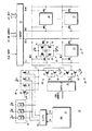
図1には、本発明によるデータ処理システム10の部分的な概略ブロック図を示す。データ処理システム10は、中央処理装置(CPU)12、メモリ14、ワード線ドライバ電源制御回路36、ヒューズブロック回路64及びレジスタ72を含む。メモリ14は、メモリアレイ15、行デコーダ46、ワード線ドライバ回路48及び列論理部62を含む。メモリアレイ15は、代表的なSRAMセル16,18,20,22を有する。メモリセル16は従来の6トランジスタセルであり、Pチャネルのプルアップトランジスタ24,26、Nチャネルのプルダウントランジスタ28,30、及びNチャネルのアクセストランジスタ32,34を含む。アレイ15のメモリセルは全てメモリセル16と同一である。ワード線ドライバ電源制御回路36は、Pチャネルトランジスタ38及びNチャネルトランジスタ40,42,44を含む複数のトランジスタと、ヒューズブロック回路64と、レジスタ72とを含む。ワード線ドライバ回路48は、ワード線ドライバ50及びワード線ドライバ52を含む。なお、データ処理システム10は、図1には示さない他の回路を含む場合もある。
FIG. 1 shows a partial schematic block diagram of a
メモリアレイ15では、メモリセルは行及び列に組織される。メモリセルの列は、ビット線ペアと、そのビット線ペアへ接続されている全てのメモリセルとを含む。例えば、「BL0」及び「BL0*」のラベルの付けられたビット線ペアと、セル16,20とは、1つの列をなす。同様に、ビット線BLM,BLM*と、メモリセル18,22とは、M+1列を有するメモリアレイにおける別の列をなす。ここでMは整数である。なお、アスタリスク(*)を有する信号名はアスタリスクを欠く同じ名称の信号の論理的な補数である。メモリアレイ15の行は、ワード線と、そのワード線へ接続されている全てのメモリセルとを含む。例えば、「WL0」のラベルの付けられたワード線と、メモリセル16,18とは、1つの行をなす。同様に、ワード線WLNと、メモリセル20,22とは、N+1行を有するメモリアレイにおける別の行をなす。ここでNは整数である。図1には2行2列しか示さないが、一般にメモリアレイは多くの行及び列を含む。
In memory array 15, memory cells are organized in rows and columns. The column of memory cells includes a bit line pair and all the memory cells connected to the bit line pair. For example, the bit line pairs labeled “BL0” and “BL0 *” and the
各々のビット線ペアは列論理部62へ接続されている。列論理部62は、例えば、列デコーダ、センスアンプ及びビット線負荷部を含む。「R/W ENABLE」のラベルの付けられた読取/書込イネーブル信号は列論理部62に対する入力として提供され、それにより、メモリアレイが書き込まれるか読み取られるかが決定される。書込操作中、「COLUMN ADDRESS」のラベルの付けられた列アドレスによって、「I/O DATA」のラベルの付けられたデータ端子でメモリアレイのいずれの列が書込データを受け取るかが選択される。読取操作中、COLUMN ADDRESSによって、いずれの列がI/O DATA端子に読取データを提供するかが選択される。行デコーダ46は、「ROW ADDRESS」のラベルの付けられた行アドレスを受け取るための、複数の入力を有する。ROW ADDRESSを受け取ることに応答して、行デコーダはメモリアレイ15へのアクセス(読取又は書込)中にワード線のうちの1つを選択するために、アドレス信号A0〜ANを提供する。アドレス信号A0〜ANの各々は、ワード線ドライバ回路50,52によって表される、対応するワード線ドライバへ提供される。示す実施形態では、ワード線ドライバはインバータとして実装される。他の実施形態では、ワード線ドライバは、例えば、非反転バッファ回路など、異なる回路であってもよい。なお、メモリ14の読取操作及び書込操作は従来の通りであるため、さらには説明しない。
Each bit line pair is connected to the
ワード線ドライバ50は、Pチャネルのプルアップトランジスタ54及びNチャネルのプルダウントランジスタ56を含む。ワード線ドライバ52は、Pチャネルのプルアップトランジスタ58及びNチャネルのプルダウントランジスタ60を含む。ワード線ドライバ50では、Nチャネルトランジスタ56のソース端子はVSSのラベルの付けられた電源電圧端子へ接続されている。トランジスタ54,56ドレインは一般的には接続されており、出力端子にワード線電圧WL0を提供する。同じように、ワード線ドライバ回路52のトランジスタ58,60は、一体に接続されている。
The
低電力動作中、ワード線ドライバ電源制御回路36はワード線ドライバ回路の各々に、電源電圧VDDより所定の電圧だけ低い電源電圧を提供する。示す実施形態では、この所定の電圧は、トランジスタのしきい電圧(VT)降下である。図1には、ワード線ドライバ電源回路36における3つのNチャネルトランジスタ40,42,44を示す。示す実施形態では、これらのトランジスタの各々は異なるVTを有するように実装されており、選択されたときに異なる電圧降下を提供する。トランジスタ40,42,44は、VDDと内部電源ノード37との間に並列に接続されている。また、Pチャネルトランジスタ54,58のソース端子も内部電源ノード37へ接続されている。他の実施形態では、3つのトランジスタ40,42,44より多くの又は少ないトランジスタが存在してよい。Nチャネルトランジスタ40,42,44のゲートは、レジスタ72へ接続されている。レジスタ72は、CPU 12によって読取及び書込が行われる複数のプログラム可能なビットを含む。CPU 12は、「SI」のラベルの付けられた、レジスタ72のビットをプログラムするためのシリアル端子と、「CLK」のラベルの付けられた、クロック信号をレジスタ72へ提供するためのクロック端子とを有する。レジスタ72の各ビットは、トランジスタ40,42,44のうちの1つに対応する。
During low power operation, the word line driver power
また、複数のヒューズ回路を有するヒューズブロック64も、Nチャネルトランジスタ40,42,44のゲートへ接続されている。なお、本発明の記載においてヒューズ回路のタイプは重要でなく、メモリに冗長性を実装するために用いられるものなど、従来のヒューズ回路であってよい。一実施形態では、ヒューズブロック回路は、VDDへ接続されている1つの端子と、Nチャネルトランジスタ(図示せず)のドレインへ接続されている第2の端子とを有する、レーザ溶断可能なヒューズ(図示せず)を含む。Nチャネルトランジスタのゲートは、データ処理システムの作動時に高にバイアスされる。Nチャネルトランジスタのドレインは、交差接続ラッチ回路(図示せず)の入力へ接続される。ヒューズが損傷していないとき、交差接続ラッチの入力は高にプルされ、交差接続ラッチの出力は論理的に低(low)となる。ヒューズが溶断されるとき、交差接続ラッチの入力は低にプルされ、Nチャネルトランジスタ40,42,44のうちの1つに対し提供される交差接続ラッチの出力は論理的に高となる。別の実施形態では、ヒューズ回路は別なように実装されてもよい。ヒューズのうちの1つが溶断されるとき、対応するヒューズ回路66,68又は70は、それぞれ対応するトランジスタ40,42又は44のゲートへ電源電圧VDDを接続する。
A
メモリ14の通常動作中、「LOW VDD」のラベルの付けられたイネーブル信号は論理的に低の電圧で提供され、トランジスタ38を導通させる。ワード線ドライバ回路48の電源電圧はPチャネルトランジスタ38を通じて提供され、ほぼVDDに等しい。ワード線WL0〜WLNのうちの1つが選択されるとき、ワード線ドライバ回路は、ほぼVDDに等しい論理的に高のワード線電圧を提供する。未選択のワード線は、ほぼグランド電位(VSS)のまま保持される。
During normal operation of
データ処理システム10の低電圧動作中、電力節約のため電源電圧が低下する。電源電圧が低くなることによって、SRAMの動作に悪影響が与えられ得る。例えば、メモリ動作の信頼性が低下する程度にメモリセルの静的ノイズマージンが低下する場合がある。より低い電源電圧にて静的ノイズマージンを増加させるため、示す実施形態では、電源電圧未満に所定の電圧だけ(例えばVDD未満にVTだけ)、ワード線電圧を低下させる。これによって静的ノイズマージンは増加するため、より低い電源電圧にて信頼性のあるメモリ動作が可能となる。
During low voltage operation of the
メモリアレイ15の試験中、レジスタ72は、トランジスタ40,42,44の各々を選択することによって、ワード線ドライバにVDD未満の異なる電源電圧を提供するために用いられる。これにより、トランジスタ40,42,44によって提供されるワード線ドライバ電圧の各々において、アレイ15のメモリセルの低VDD動作が判定される。トランジスタ40,42又は44のいずれがメモリ14の最良の低電圧動作を提供するかが判定されるとき、最良の低VDD動作を提供するトランジスタ40,42又は44のゲートに対応するヒューズ回路66,68又は70が溶断される。ヒューズ回路のヒューズは電気的に溶断されるか、或いは、レーザ溶断され得る。次いで、電源電圧が存在するとき、溶断したヒューズ回路は、そのトランジスタのゲートを永続的にバイアスする。
During testing of the memory array 15, the register 72 is used to provide different power supply voltages below V DD to the word line driver by selecting each of the
データ処理システム10が低電力モードに入るとき、イネーブル信号LOW VDDは論理的に高の電圧としてアサートされ、Pチャネルトランジスタ38は、ほぼ導通しなくなる。なお、好適には、イネーブル信号LOW VDDはデータ処理システム10の外部のソースによって提供される。しかしながら、他の実施形態では、CPU 12などデータ処理システム10上の別の回路又は図1には示さない異なる回路によって、イネーブル信号LOW VDDが提供されてもよい。ワード線ドライバ回路用の電源は、Nチャネルトランジスタ40,42,44のうちの選択された1つを介して提供される。例として、データ処理システム10の電源電圧が、通常、公称1.2ボルトである場合、低電力モード中にVDDに対し提供される電源電圧は0.8ボルト以下である。Nチャネルトランジスタ40,42,44のしきい電圧は、例えば、それぞれ約40ミリボルト(mV),60mV,80mVであるように選択される。例えば、Nチャネルトランジスタ40によって提供される電圧が最良の低電力動作を提供する場合、ヒューズ回路66が溶断され、ワード線電圧WL0は、ほぼVDDから40mVを減じたものに等しい。
When the
SRAMビットセル設計において、1つの重要な基準はベータ(β)比と呼ばれる。メモリセルのベータ比は、アクセストランジスタの幅/長さ(W/L)比に対するプルダウントランジスタのW/L比である。ベータ比は、アクセス速度及びセル安定性に影響を与える。一般には、所与のセルサイズにおいて、ベータ比が高くなると、アクセス速度はより低くなるが、セル安定性が改良される。ワード線電圧を低下させると、ベータ比を増大する効果がある。 In SRAM bit cell design, one important criterion is called the beta (β) ratio. The beta ratio of the memory cell is the W / L ratio of the pull-down transistor to the width / length (W / L) ratio of the access transistor. The beta ratio affects access speed and cell stability. In general, for a given cell size, a higher beta ratio results in a lower access speed but improved cell stability. Lowering the word line voltage has the effect of increasing the beta ratio.
本発明の他の実施形態では、低電圧動作中のワード線電圧が異なる手法によって制御されてもよい。例えば、トランジスタ40,42,44は、分圧器と置き換えられてもよい。また、トランジスタ40,42,44の代わりに、複数の直列に接続されたトランジスタが用いられてもよい。また、電源電圧が外部的に提供されてもよい。
In other embodiments of the present invention, the word line voltage during low voltage operation may be controlled by different techniques. For example,
複数のワード線ドライバ電源トランジスタを用い、低電圧動作中にVDD未満のワード線電圧を提供することによって、静的ノイズマージンが改良されるため、メモリの信頼性が改良される。また、本発明によって、通常動作モード中の高速動作に対するVDDにほぼ等しいワード線電圧でメモリを動作させることが可能となる。 By using a plurality of word line driver power supply transistors and providing a word line voltage below V DD during low voltage operation, the static noise margin is improved, thus improving the reliability of the memory. The present invention also allows the memory to operate with a word line voltage substantially equal to VDD for high speed operation during the normal operation mode.
Claims (4)
前記ワード線に接続されるとともに第2の電源ノードに接続されている複数のワード線ドライバと、
第1の電源ノードへ接続されている入力部と、第2の電源ノードへ接続されている出力部とを有し、前記電源電圧の低下を示す低供給電圧信号に応答して、入力部に対する電圧に関連して出力部に対する電圧を低下させる電圧低下回路と、
複数のヒューズを含み、前記電圧低下回路に接続されているヒューズブロック回路と、を備え、
前記電圧低下回路は、
低供給電圧信号がアクティブであることに応答して、第1の電源ノードと第2の電源ノードとの間から分断される第1のトランジスタと、
前記複数のヒューズのうちの対応するヒューズに各々接続されており、互いに異なる電圧降下を提供する複数の第2のトランジスタと、を含み、
前記複数のヒューズのうちの一つが溶断している状態で低供給電圧信号がアクティブとなるときに、溶断したヒューズに対応する第2のトランジスタが導通して第1の電源ノードと第2の電源ノードとの間へ接続される、回路。A memory array including memory cells connected to a word line and a bit line is connected to a first power supply node for receiving a power supply voltage,
A plurality of word line drivers with being connected to the second power supply node is connected to said word line,
It has an input portion connected to the first power supply node and an output connected to a second power supply node, in response to the low supply voltage signal indicating the drop in the power supply voltage, the input unit a voltage drop circuit voltage Ru reduces the relative output unit in relation to the voltage,
A fuse block circuit including a plurality of fuses and connected to the voltage drop circuit,
The voltage drop circuit is
A first transistor that is decoupled from between the first power supply node and the second power supply node in response to the low supply voltage signal being active;
A plurality of second transistors each connected to a corresponding one of the plurality of fuses and providing a different voltage drop;
When a low supply voltage signal becomes active while one of the plurality of fuses is blown, the second transistor corresponding to the blown fuse is turned on, and the first power supply node and the second power supply are turned on. A circuit connected to a node .
電源電圧を受け取るための第1の電源ノードに接続されるとともにワード線及びビット線に接続されているメモリセルを有するメモリアレイと、
前記ワード線に接続されるとともに第2の電源ノードに接続されており、通常動作モード中、第1の電源ノードに対し印加される電圧を第2の電源ノードに提供し、かつ、低電力動作モード中、第1の電源ノードに対し印加される電圧未満に低下した電圧を第2の電源ノードに提供するためのワード線ドライバ手段と、
複数のヒューズを含み、前記ワード線ドライバ手段に接続されているヒューズブロック回路と、を備え、
前記ワード線ドライバ手段は、
低電力動作モードに入ることに応答して、第1の電源ノードと第2の電源ノードとの間から分断される第1のトランジスタと、
前記複数のヒューズのうちの対応するヒューズに各々接続されており、互いに異なる電圧降下を提供する複数の第2のトランジスタと、を含み、
前記複数のヒューズのうちの一つが溶断している状態で低電力動作モードに入ったときに、溶断したヒューズに対応する第2のトランジスタが導通して第1の電源ノードと第2の電源ノードとの間に接続される、回路。A circuit having a normal operating mode and a low power operating mode with a reduced power supply voltage indicated by a low supply voltage signal,
A memory array having memory cells connected to a word line and a bit line is connected to a first power supply node for receiving a power supply voltage,
Wherein it is connected to a word line connected to the second power supply node, during the normal operation mode, and provides a voltage applied to the first power supply node to the second power supply node, and low power operation Word line driver means for providing to the second power supply node a voltage that drops below the voltage applied to the first power supply node during the mode;
A fuse block circuit including a plurality of fuses and connected to the word line driver means,
The word line driver means includes:
A first transistor decoupled from between the first power supply node and the second power supply node in response to entering the low power mode of operation;
A plurality of second transistors each connected to a corresponding one of the plurality of fuses and providing a different voltage drop;
When the low-power operation mode is entered while one of the plurality of fuses is blown, the second transistor corresponding to the blown fuse is turned on so that the first power supply node and the second power supply node Connected between and the circuit.
前記ワード線に接続されるとともに第2の電源ノードに接続されている複数のワード線ドライバと、
第1の電源ノード及び第2の電源ノードへ接続されており、通常動作モードにおいて第2の電源ノードに対し第1の供給電圧を提供し、かつ、前記電源電圧が低下される第2の動作モードに入ることに応答して、第2の動作モード中、前記第1の電源ノードに対して提供される電圧未満の電圧を第2の電源ノードに対し提供するための電圧制御手段と、
複数のヒューズを含み、前記電圧制御手段に接続されているヒューズブロック回路と、を備え、
前記電圧制御手段は、
第2の動作モードに入ることに応答して、第1の電源ノードと第2の電源ノードとの間から分断される第1のトランジスタと、
前記複数のヒューズのうちの対応するヒューズに各々接続されており、互いに異なる電圧降下を提供する複数の第2のトランジスタと、を含み、
前記複数のヒューズのうちの一つが溶断している状態で第2の動作モードに入ったときに、溶断したヒューズに対応する第2のトランジスタが導通して第1の電源ノードと第2の電源ノードとの間に接続される、回路。A memory array having memory cells connected to a word line and a bit line is connected to a first power supply node for receiving a power supply voltage,
A plurality of word line drivers with being connected to the second power supply node is connected to said word line,
It is connected to the first power supply node and the second power supply node to provide a first supply voltage to the second power supply node in the normal operation mode and a second operation in which the power supply voltage is lowered in response to entering the mode, the voltage control means for providing during the second mode of operation, a voltage lower than the voltage provided by to said first power supply node to the second power supply node,
A fuse block circuit including a plurality of fuses and connected to the voltage control means,
The voltage control means includes
A first transistor decoupled from between the first power supply node and the second power supply node in response to entering the second operation mode;
A plurality of second transistors each connected to a corresponding one of the plurality of fuses and providing a different voltage drop;
When the second operation mode is entered while one of the plurality of fuses is blown, the second transistor corresponding to the blown fuse is turned on, and the first power supply node and the second power supply are turned on. A circuit connected to a node .
第1の動作モード中、電圧制御手段によって、第1の電源ノード及び第2の電源ノードに対しほぼ等しい第1のレベルの電圧を印加する第1電圧印加工程と、
第1の電源ノードに対し第1のレベル未満の第2のレベルの電圧が印加される第2の動作モード中、前記電圧制御手段によって、第2の電源ノードに対し第2のレベル未満の電圧を印加する第2電圧印加工程と、を備え、
前記電圧制御手段には、複数のヒューズを含むヒューズブロック回路が接続され、
前記電圧制御手段は、前記第1の動作モード時に第1の電源ノードと第2の電源ノードとの間に接続される第1のトランジスタと、前記複数のヒューズのうちの対応するヒューズに各々接続されており、互いに異なる電圧降下を提供する複数の第2のトランジスタと、を含み、
前記第2電圧印加工程は、
前記第2の動作モードに入ることに応答して、第1の電源ノードと第2の電源ノードとの間から第1のトランジスタを分断する工程と、
前記複数のヒューズのうちの一つが溶断している状態で第2の動作モードに入ったときに、溶断したヒューズに対応する第2のトランジスタを導通させて第1の電源ノードと第2の電源ノードとの間に接続する工程と、
を含む、動作方法。A memory array having memory cells connected to a word line and a bit line is connected to a first power supply node for receiving a power supply voltage, is connected to a second power supply node is connected to a word line a plurality of word line drivers are, a method of operating a memory comprising,
A first voltage applying step of applying a substantially equal first level voltage to the first power supply node and the second power supply node by the voltage control means during the first operation mode;
During a second operation mode in which a second level voltage less than the first level is applied to the first power supply node , the voltage control means causes the voltage less than the second level to be applied to the second power supply node. and a second voltage application step of applying,
A fuse block circuit including a plurality of fuses is connected to the voltage control means,
The voltage control means is connected to a first transistor connected between a first power supply node and a second power supply node in the first operation mode, and to a corresponding fuse of the plurality of fuses, respectively. A plurality of second transistors that provide different voltage drops from each other; and
The second voltage application step includes
In response to entering the second operating mode, separating the first transistor from between the first power supply node and the second power supply node;
When the second operation mode is entered while one of the plurality of fuses is blown, the first power supply node and the second power supply are turned on by turning on the second transistor corresponding to the blown fuse. Connecting to a node;
Including an operation method.
Applications Claiming Priority (3)
| Application Number | Priority Date | Filing Date | Title |
|---|---|---|---|
| US10/991,910 US7085175B2 (en) | 2004-11-18 | 2004-11-18 | Word line driver circuit for a static random access memory and method therefor |
| US10/991,910 | 2004-11-18 | ||
| PCT/US2005/038468 WO2006055190A1 (en) | 2004-11-18 | 2005-10-25 | Word line driver circuit for a static random access memory and method therefor |
Publications (3)
| Publication Number | Publication Date |
|---|---|
| JP2008521157A JP2008521157A (en) | 2008-06-19 |
| JP2008521157A5 JP2008521157A5 (en) | 2008-12-11 |
| JP4988588B2 true JP4988588B2 (en) | 2012-08-01 |
Family
ID=36386078
Family Applications (1)
| Application Number | Title | Priority Date | Filing Date |
|---|---|---|---|
| JP2007543071A Active JP4988588B2 (en) | 2004-11-18 | 2005-10-25 | Word line driver circuit for static random access memory |
Country Status (5)
| Country | Link |
|---|---|
| US (1) | US7085175B2 (en) |
| JP (1) | JP4988588B2 (en) |
| KR (1) | KR101227291B1 (en) |
| CN (1) | CN101040343B (en) |
| WO (1) | WO2006055190A1 (en) |
Families Citing this family (32)
| Publication number | Priority date | Publication date | Assignee | Title |
|---|---|---|---|---|
| US7226857B2 (en) | 2004-07-30 | 2007-06-05 | Micron Technology, Inc. | Front-end processing of nickel plated bond pads |
| DE102004042362B3 (en) * | 2004-09-01 | 2006-03-30 | Infineon Technologies Ag | Integrated semiconductor memory with at least one word line and method |
| US7355905B2 (en) | 2005-07-01 | 2008-04-08 | P.A. Semi, Inc. | Integrated circuit with separate supply voltage for memory that is different from logic circuit supply voltage |
| JP5100035B2 (en) | 2005-08-02 | 2012-12-19 | ルネサスエレクトロニクス株式会社 | Semiconductor memory device |
| JP5158624B2 (en) | 2006-08-10 | 2013-03-06 | ルネサスエレクトロニクス株式会社 | Semiconductor memory device |
| JP2008047698A (en) * | 2006-08-16 | 2008-02-28 | Renesas Technology Corp | Semiconductor storage device |
| US7440313B2 (en) * | 2006-11-17 | 2008-10-21 | Freescale Semiconductor, Inc. | Two-port SRAM having improved write operation |
| JP5057757B2 (en) * | 2006-11-30 | 2012-10-24 | 株式会社東芝 | Semiconductor integrated circuit |
| JP5068088B2 (en) * | 2007-02-26 | 2012-11-07 | ルネサスエレクトロニクス株式会社 | Semiconductor memory device |
| JP5064089B2 (en) * | 2007-04-12 | 2012-10-31 | パナソニック株式会社 | Semiconductor integrated circuit |
| JP5224040B2 (en) * | 2008-04-01 | 2013-07-03 | ルネサスエレクトロニクス株式会社 | Semiconductor integrated circuit device |
| JP5262454B2 (en) * | 2008-09-01 | 2013-08-14 | 富士通セミコンダクター株式会社 | Semiconductor memory |
| US7903483B2 (en) * | 2008-11-21 | 2011-03-08 | Freescale Semiconductor, Inc. | Integrated circuit having memory with configurable read/write operations and method therefor |
| TWI404065B (en) * | 2009-02-13 | 2013-08-01 | Univ Hsiuping Sci & Tech | Single port sram having a higher voltage word line in writing operation |
| US7864617B2 (en) * | 2009-02-19 | 2011-01-04 | Freescale Semiconductor, Inc. | Memory with reduced power supply voltage for a write operation |
| US8379466B2 (en) * | 2009-03-31 | 2013-02-19 | Freescale Semiconductor, Inc. | Integrated circuit having an embedded memory and method for testing the memory |
| US8315117B2 (en) * | 2009-03-31 | 2012-11-20 | Freescale Semiconductor, Inc. | Integrated circuit memory having assisted access and method therefor |
| US8634263B2 (en) * | 2009-04-30 | 2014-01-21 | Freescale Semiconductor, Inc. | Integrated circuit having memory repair information storage and method therefor |
| KR101068571B1 (en) * | 2009-07-03 | 2011-09-30 | 주식회사 하이닉스반도체 | Semiconductor memory device |
| US8514611B2 (en) * | 2010-08-04 | 2013-08-20 | Freescale Semiconductor, Inc. | Memory with low voltage mode operation |
| US8228713B2 (en) | 2010-09-28 | 2012-07-24 | International Business Machines Corporation | SRAM having wordline up-level voltage adjustable to assist bitcell stability and design structure for same |
| US8582351B2 (en) | 2010-09-28 | 2013-11-12 | International Business Machines Corporation | Methods and systems for adjusting wordline up-level voltage to improve production yield relative to SRAM-cell stability |
| KR101799482B1 (en) * | 2010-12-29 | 2017-11-20 | 삼성전자주식회사 | Static random access memory device including write assist circuit |
| JP5653856B2 (en) * | 2011-07-21 | 2015-01-14 | ルネサスエレクトロニクス株式会社 | Semiconductor device |
| US8811110B2 (en) * | 2012-06-28 | 2014-08-19 | Intel Corporation | Configuration for power reduction in DRAM |
| US8804449B2 (en) | 2012-09-06 | 2014-08-12 | Micron Technology, Inc. | Apparatus and methods to provide power management for memory devices |
| KR102083488B1 (en) | 2013-09-12 | 2020-03-02 | 삼성전자 주식회사 | Test interface board and test system including the same |
| CN103531229A (en) * | 2013-10-18 | 2014-01-22 | 上海工程技术大学 | Static random access memory |
| JP6424448B2 (en) * | 2014-03-28 | 2018-11-21 | 株式会社ソシオネクスト | Semiconductor memory device |
| US9455023B1 (en) * | 2015-10-14 | 2016-09-27 | Oracle International Corporation | Wordline under-driving using a virtual power network |
| IT201600121631A1 (en) | 2016-11-30 | 2018-05-30 | St Microelectronics Srl | STAGE-CHANGING MEMORY DEVICE WITH A HIGH-SPEED WORD LINE PILOT CIRCUIT |
| JP2020042878A (en) * | 2018-09-12 | 2020-03-19 | 株式会社東芝 | Semiconductor memory device |
Family Cites Families (20)
| Publication number | Priority date | Publication date | Assignee | Title |
|---|---|---|---|---|
| JP2893708B2 (en) * | 1989-04-06 | 1999-05-24 | ソニー株式会社 | Semiconductor memory device |
| JPH04339398A (en) * | 1991-01-08 | 1992-11-26 | Mitsubishi Electric Corp | Address input first stage circuit for semiconductor memory |
| JPH05303892A (en) * | 1992-04-02 | 1993-11-16 | Nec Corp | Semiconductor storage circuit |
| JPH0620477A (en) * | 1992-06-30 | 1994-01-28 | Nec Corp | Semiconductor static random access memory device |
| TW243531B (en) * | 1993-09-03 | 1995-03-21 | Motorola Inc | |
| JP2639328B2 (en) * | 1993-11-12 | 1997-08-13 | 日本電気株式会社 | Trimming method and circuit |
| JPH07280889A (en) * | 1994-04-12 | 1995-10-27 | Oki Electric Ind Co Ltd | Method of voltage margin test for device |
| JPH09326194A (en) * | 1996-06-05 | 1997-12-16 | Mitsubishi Electric Corp | Step-down circuit |
| KR100290283B1 (en) * | 1998-10-30 | 2001-05-15 | 윤종용 | Nonvolatile semiconductor memory device and word line driving method thereof |
| JP3380852B2 (en) * | 1999-04-13 | 2003-02-24 | 松下電器産業株式会社 | Semiconductor storage device |
| JP2001014859A (en) * | 1999-06-30 | 2001-01-19 | Toshiba Corp | Semiconductor device |
| JP2002042476A (en) * | 2000-07-25 | 2002-02-08 | Mitsubishi Electric Corp | Static semiconductor memory |
| US6512705B1 (en) * | 2001-11-21 | 2003-01-28 | Micron Technology, Inc. | Method and apparatus for standby power reduction in semiconductor devices |
| JP4162076B2 (en) * | 2002-05-30 | 2008-10-08 | 株式会社ルネサステクノロジ | Semiconductor memory device |
| JP4370100B2 (en) * | 2003-01-10 | 2009-11-25 | パナソニック株式会社 | Semiconductor memory device |
| US6827275B2 (en) * | 2003-01-22 | 2004-12-07 | Ufp Technologies, Inc. | Method of tracking and marking tools |
| JP4258709B2 (en) * | 2003-05-16 | 2009-04-30 | 東洋紡績株式会社 | Polyolefin film for laminating, laminated film and packaging bag using the same |
| JP2005108307A (en) * | 2003-09-29 | 2005-04-21 | Nec Electronics Corp | Semiconductor storage device |
| JP2005303892A (en) * | 2004-04-15 | 2005-10-27 | Sharp Corp | Communication device |
| JP2006020477A (en) * | 2004-07-05 | 2006-01-19 | Asmo Co Ltd | Rotary electric machine, electric power-steering motor, and rotary electric machine manufacturing method |
-
2004
- 2004-11-18 US US10/991,910 patent/US7085175B2/en active Active
-
2005
- 2005-10-25 KR KR1020077011213A patent/KR101227291B1/en active IP Right Grant
- 2005-10-25 CN CN2005800347232A patent/CN101040343B/en active Active
- 2005-10-25 JP JP2007543071A patent/JP4988588B2/en active Active
- 2005-10-25 WO PCT/US2005/038468 patent/WO2006055190A1/en active Application Filing
Also Published As
| Publication number | Publication date |
|---|---|
| WO2006055190A1 (en) | 2006-05-26 |
| KR101227291B1 (en) | 2013-01-29 |
| US7085175B2 (en) | 2006-08-01 |
| CN101040343A (en) | 2007-09-19 |
| KR20070084313A (en) | 2007-08-24 |
| JP2008521157A (en) | 2008-06-19 |
| US20060104107A1 (en) | 2006-05-18 |
| CN101040343B (en) | 2013-11-20 |
Similar Documents
| Publication | Publication Date | Title |
|---|---|---|
| JP4988588B2 (en) | Word line driver circuit for static random access memory | |
| US7502273B2 (en) | Two-port SRAM with a high speed sensing scheme | |
| US6903962B2 (en) | Semiconductor memory device capable of controlling potential level of power supply line and/or ground line | |
| JP4330396B2 (en) | Semiconductor memory device | |
| JP4768437B2 (en) | Semiconductor memory device | |
| TW588358B (en) | Semiconductor memory device and its refreshing method | |
| US5969995A (en) | Static semiconductor memory device having active mode and sleep mode | |
| JP2007172715A (en) | Semiconductor memory device and its control method | |
| JP5104123B2 (en) | Semiconductor memory | |
| US8964451B2 (en) | Memory cell system and method | |
| US20180053546A1 (en) | Semiconductor device, test program, and test method | |
| US7630273B2 (en) | Semiconductor integrated circuit | |
| JP2008027493A (en) | Semiconductor memory device | |
| JP3317746B2 (en) | Semiconductor storage device | |
| JP3015652B2 (en) | Semiconductor memory device | |
| US7821817B2 (en) | Semiconductor storage device | |
| US20040042326A1 (en) | Static semiconductor memory device and method of controlling the same | |
| US7684231B2 (en) | Methods and apparatus for low power SRAM based on stored data | |
| US20060092720A1 (en) | Semiconductor memory | |
| JP2008176907A (en) | Semiconductor memory device | |
| JP2011146121A (en) | Semiconductor memory and control method for the same | |
| JP2008065863A (en) | Semiconductor memory device | |
| JP2001023399A (en) | Semiconductor memory | |
| JP2004280956A (en) | Semiconductor memory device |
Legal Events
| Date | Code | Title | Description |
|---|---|---|---|
| A521 | Request for written amendment filed |
Free format text: JAPANESE INTERMEDIATE CODE: A523 Effective date: 20081021 |
|
| A621 | Written request for application examination |
Free format text: JAPANESE INTERMEDIATE CODE: A621 Effective date: 20081021 |
|
| A977 | Report on retrieval |
Free format text: JAPANESE INTERMEDIATE CODE: A971007 Effective date: 20110516 |
|
| A131 | Notification of reasons for refusal |
Free format text: JAPANESE INTERMEDIATE CODE: A131 Effective date: 20110531 |
|
| A601 | Written request for extension of time |
Free format text: JAPANESE INTERMEDIATE CODE: A601 Effective date: 20110831 |
|
| A602 | Written permission of extension of time |
Free format text: JAPANESE INTERMEDIATE CODE: A602 Effective date: 20110907 |
|
| A521 | Request for written amendment filed |
Free format text: JAPANESE INTERMEDIATE CODE: A523 Effective date: 20110929 |
|
| TRDD | Decision of grant or rejection written | ||
| A01 | Written decision to grant a patent or to grant a registration (utility model) |
Free format text: JAPANESE INTERMEDIATE CODE: A01 Effective date: 20120403 |
|
| A01 | Written decision to grant a patent or to grant a registration (utility model) |
Free format text: JAPANESE INTERMEDIATE CODE: A01 |
|
| A61 | First payment of annual fees (during grant procedure) |
Free format text: JAPANESE INTERMEDIATE CODE: A61 Effective date: 20120426 |
|
| R150 | Certificate of patent or registration of utility model |
Ref document number: 4988588 Country of ref document: JP Free format text: JAPANESE INTERMEDIATE CODE: R150 Free format text: JAPANESE INTERMEDIATE CODE: R150 |
|
| FPAY | Renewal fee payment (event date is renewal date of database) |
Free format text: PAYMENT UNTIL: 20150511 Year of fee payment: 3 |
|
| R250 | Receipt of annual fees |
Free format text: JAPANESE INTERMEDIATE CODE: R250 |
|
| R250 | Receipt of annual fees |
Free format text: JAPANESE INTERMEDIATE CODE: R250 |
|
| R250 | Receipt of annual fees |
Free format text: JAPANESE INTERMEDIATE CODE: R250 |
|
| S533 | Written request for registration of change of name |
Free format text: JAPANESE INTERMEDIATE CODE: R313533 |
|
| R350 | Written notification of registration of transfer |
Free format text: JAPANESE INTERMEDIATE CODE: R350 |
|
| R250 | Receipt of annual fees |
Free format text: JAPANESE INTERMEDIATE CODE: R250 |
|
| R250 | Receipt of annual fees |
Free format text: JAPANESE INTERMEDIATE CODE: R250 |
|
| R250 | Receipt of annual fees |
Free format text: JAPANESE INTERMEDIATE CODE: R250 |
|
| R250 | Receipt of annual fees |
Free format text: JAPANESE INTERMEDIATE CODE: R250 |
|
| R250 | Receipt of annual fees |
Free format text: JAPANESE INTERMEDIATE CODE: R250 |
|
| R250 | Receipt of annual fees |
Free format text: JAPANESE INTERMEDIATE CODE: R250 |
|
| R250 | Receipt of annual fees |
Free format text: JAPANESE INTERMEDIATE CODE: R250 |