JP4984869B2 - Reception circuit, electronic device, and noise canceling method - Google Patents
Reception circuit, electronic device, and noise canceling method Download PDFInfo
- Publication number
- JP4984869B2 JP4984869B2 JP2006335454A JP2006335454A JP4984869B2 JP 4984869 B2 JP4984869 B2 JP 4984869B2 JP 2006335454 A JP2006335454 A JP 2006335454A JP 2006335454 A JP2006335454 A JP 2006335454A JP 4984869 B2 JP4984869 B2 JP 4984869B2
- Authority
- JP
- Japan
- Prior art keywords
- signal
- unit
- circuit
- cancel
- intermediate frequency
- Prior art date
- Legal status (The legal status is an assumption and is not a legal conclusion. Google has not performed a legal analysis and makes no representation as to the accuracy of the status listed.)
- Expired - Fee Related
Links
Images


Classifications
-
- H—ELECTRICITY
- H04—ELECTRIC COMMUNICATION TECHNIQUE
- H04B—TRANSMISSION
- H04B1/00—Details of transmission systems, not covered by a single one of groups H04B3/00 - H04B13/00; Details of transmission systems not characterised by the medium used for transmission
- H04B1/06—Receivers
-
- H—ELECTRICITY
- H04—ELECTRIC COMMUNICATION TECHNIQUE
- H04B—TRANSMISSION
- H04B1/00—Details of transmission systems, not covered by a single one of groups H04B3/00 - H04B13/00; Details of transmission systems not characterised by the medium used for transmission
- H04B1/69—Spread spectrum techniques
- H04B1/707—Spread spectrum techniques using direct sequence modulation
- H04B1/7097—Interference-related aspects
- H04B1/7103—Interference-related aspects the interference being multiple access interference
- H04B1/7107—Subtractive interference cancellation
-
- G—PHYSICS
- G01—MEASURING; TESTING
- G01S—RADIO DIRECTION-FINDING; RADIO NAVIGATION; DETERMINING DISTANCE OR VELOCITY BY USE OF RADIO WAVES; LOCATING OR PRESENCE-DETECTING BY USE OF THE REFLECTION OR RERADIATION OF RADIO WAVES; ANALOGOUS ARRANGEMENTS USING OTHER WAVES
- G01S19/00—Satellite radio beacon positioning systems; Determining position, velocity or attitude using signals transmitted by such systems
- G01S19/01—Satellite radio beacon positioning systems transmitting time-stamped messages, e.g. GPS [Global Positioning System], GLONASS [Global Orbiting Navigation Satellite System] or GALILEO
- G01S19/13—Receivers
- G01S19/21—Interference related issues ; Issues related to cross-correlation, spoofing or other methods of denial of service
-
- H—ELECTRICITY
- H04—ELECTRIC COMMUNICATION TECHNIQUE
- H04B—TRANSMISSION
- H04B1/00—Details of transmission systems, not covered by a single one of groups H04B3/00 - H04B13/00; Details of transmission systems not characterised by the medium used for transmission
- H04B1/06—Receivers
- H04B1/10—Means associated with receiver for limiting or suppressing noise or interference
- H04B1/12—Neutralising, balancing, or compensation arrangements
- H04B1/123—Neutralising, balancing, or compensation arrangements using adaptive balancing or compensation means
- H04B1/126—Neutralising, balancing, or compensation arrangements using adaptive balancing or compensation means having multiple inputs, e.g. auxiliary antenna for receiving interfering signal
-
- H—ELECTRICITY
- H04—ELECTRIC COMMUNICATION TECHNIQUE
- H04B—TRANSMISSION
- H04B2201/00—Indexing scheme relating to details of transmission systems not covered by a single group of H04B3/00 - H04B13/00
- H04B2201/69—Orthogonal indexing scheme relating to spread spectrum techniques in general
- H04B2201/707—Orthogonal indexing scheme relating to spread spectrum techniques in general relating to direct sequence modulation
- H04B2201/70715—Orthogonal indexing scheme relating to spread spectrum techniques in general relating to direct sequence modulation with application-specific features
Landscapes
- Engineering & Computer Science (AREA)
- Computer Networks & Wireless Communication (AREA)
- Signal Processing (AREA)
- Radar, Positioning & Navigation (AREA)
- Remote Sensing (AREA)
- Physics & Mathematics (AREA)
- General Physics & Mathematics (AREA)
- Noise Elimination (AREA)
- Telephone Function (AREA)
Description
本発明は、受信回路、電子機器及びノイズキャンセル方法に関する。 The present invention relates to a receiving circuit , an electronic device, and a noise canceling method .
受信回路を内蔵した電子機器において、受信回路の近傍に配置されている電子回路の回路動作に伴う電磁場の変化に起因して交流信号が発生し、これが受信回路側に回り込んで、妨害波として受信信号に混在してしまう場合がある。かかる現象は、信号劣化の大きな要因となるため、受信信号に重畳された妨害波を除去するための様々な技術が考案されている。 In an electronic device with a built-in receiver circuit, an AC signal is generated due to a change in the electromagnetic field due to the circuit operation of the electronic circuit arranged in the vicinity of the receiver circuit, which wraps around to the receiver circuit side as an interference wave It may be mixed in the received signal. Since this phenomenon is a major cause of signal degradation, various techniques have been devised for removing the interference wave superimposed on the received signal.
その一例として、特許文献1には、電子回路からの発生信号の位相を遅延線を用いて反転させることで、当該発生信号を打ち消す信号(以下、「キャンセル信号」と称す。)を生成して、妨害波を除去する技術が開示されている。
ところで、アンテナ等の受信部で受信される信号は微弱な信号であり、増幅によって信号レベルを引き上げて信号処理を行うのが一般的である。しかし、特許文献1に開示されている技術では、増幅段の前の、アンテナと信号処理系統とを接続する信号線の途中位置に遅延線の接点を設け、受信直後の微弱な信号にキャンセル信号を加算する構成をとっている。
By the way, a signal received by a receiving unit such as an antenna is a weak signal, and signal processing is generally performed by raising the signal level by amplification. However, in the technique disclosed in
このため、加算するキャンセル信号の信号レベルを精確に制御し、微弱な受信信号に混在している妨害波成分を適切に打ち消す必要があった。キャンセル信号の信号レベルが不適切である場合、妨害波成分を打ち消すのに十分な信号レベルを超過した過度のキャンセル信号によって、逆に妨害波成分が増加してしまい、受信感度が劣化してしまうおそれがあった。 For this reason, it is necessary to accurately control the signal level of the cancel signal to be added and appropriately cancel the interference wave component mixed in the weak received signal. If the signal level of the cancel signal is inappropriate, the interference signal component increases due to an excessive cancel signal that exceeds the signal level sufficient to cancel the interference signal component, and the reception sensitivity deteriorates. There was a fear.
本発明は、上述した課題に鑑みて為されたものである。 The present invention has been made in view of the above-described problems.
以上の課題を解決するための第1の発明は、無線信号を受信する受信部近傍の電子回路からの発生信号を打ち消すキャンセル信号を生成するキャンセル信号生成部と、前記受信部により受信された受信信号の信号処理系統の途中所定位置で、該信号処理系統の信号に、前記キャンセル信号生成部により生成されたキャンセル信号を加算する加算部とを備えた受信回路である。 According to a first aspect of the present invention, there is provided a cancel signal generator for generating a cancel signal for canceling a generated signal from an electronic circuit in the vicinity of a receiver for receiving a radio signal, and a reception received by the receiver. A receiving circuit including an adder that adds a cancel signal generated by the cancel signal generator to a signal of the signal processing system at a predetermined position in the signal processing system of the signal.
この第1の発明によれば、受信部により受信された受信信号の信号処理系統の途中所定位置で、該信号処理系統の信号にキャンセル信号生成部で生成されたキャンセル信号が加算されることで、受信信号に重畳されたノイズがキャンセルされる。従って、信号処理系統の信号レベルが高い状態でキャンセル信号が加算されるため、アンテナの直後で加算する場合に比べて、キャンセル信号の信号レベルの調整を簡単に行うことができる。 According to the first aspect of the present invention, the cancel signal generated by the cancel signal generation unit is added to the signal of the signal processing system at a predetermined position in the signal processing system of the reception signal received by the reception unit. The noise superimposed on the received signal is canceled. Accordingly, since the cancel signal is added in a state where the signal level of the signal processing system is high, the signal level of the cancel signal can be easily adjusted as compared with the case where the signal is added immediately after the antenna.
また、第2の発明として、第1の発明の受信回路であって、局部発振信号生成部と、前記局部発振信号生成部により生成された局部発振信号を前記受信部により受信された受信信号に乗算することで、当該受信信号を中間周波数の信号に変換して前記信号処理系統の後段に出力する中間周波変換部と、前記中間周波変換部から出力された信号のうち、前記無線信号の前記中間周波数に対応する帯域を通過させるフィルタ部と、を更に備えるとともに、前記キャンセル信号生成部は、前記局部発振信号生成部により生成された局部発振信号の位相を180度移相する移相部を有し、この移相部により移相された信号を前記発生信号に乗算することで前記キャンセル信号を生成し、前記加算部は、前記フィルタ部の前で、前記中間周波変換部から出力される中間周波数の信号に前記生成されたキャンセル信号を加算する受信回路を構成してもよい。 Further, as a second invention, the receiving circuit according to the first invention, wherein a local oscillation signal generation unit and a local oscillation signal generated by the local oscillation signal generation unit are converted into a reception signal received by the reception unit. By multiplying, the received signal is converted to an intermediate frequency signal and output to the subsequent stage of the signal processing system, and among the signals output from the intermediate frequency converter, the radio signal A filter unit that passes a band corresponding to the intermediate frequency, and the cancellation signal generation unit includes a phase shift unit that shifts the phase of the local oscillation signal generated by the local oscillation signal generation unit by 180 degrees. And the cancellation signal is generated by multiplying the generated signal by the signal phase-shifted by the phase-shift unit, and the adder unit is connected to the intermediate frequency converter unit before the filter unit. The cancellation signals the generated intermediate frequency of the signal power may be configured to receive circuit for adding.
この第2の発明によれば、受信部により受信された信号が、中間周波変換部において局部発振信号と乗算されることで、中間周波数の信号に変換される。一方、キャンセル信号生成部では、受信部近傍の電子回路からの発生信号に、移相部において180度移相された局部発振信号が乗算されることで、キャンセル信号が生成される。そして、中間周波変換部で変換された中間周波数の信号が、キャンセル信号生成部で生成されたキャンセル信号と加算された後、無線信号の中間周波数に対応する帯域を通過させるフィルタ部に出力される。 According to the second aspect of the invention, the signal received by the receiving unit is converted into an intermediate frequency signal by being multiplied by the local oscillation signal in the intermediate frequency converting unit. On the other hand, the cancel signal generation unit multiplies the generated signal from the electronic circuit in the vicinity of the reception unit by the local oscillation signal phase-shifted by 180 degrees in the phase shift unit, thereby generating a cancel signal. Then, the intermediate frequency signal converted by the intermediate frequency conversion unit is added to the cancel signal generated by the cancel signal generation unit, and then output to the filter unit that passes the band corresponding to the intermediate frequency of the radio signal. .
受信部近傍の電子回路からの発生信号には、様々な周波数の信号が含まれており、信号レベルも一定ではない。一方、局部発振信号は、周波数が一定であり、信号レベルも一定であることから、移相を行うことは容易である。そこで、第2の発明によれば、移相した局部発振信号を乗算する構成により、電子回路からの発生信号の移相を簡易に実現することが可能となる。 A signal generated from an electronic circuit in the vicinity of the receiving unit includes signals of various frequencies, and the signal level is not constant. On the other hand, since the local oscillation signal has a constant frequency and a constant signal level, it is easy to perform phase shifting. Therefore, according to the second invention, it is possible to easily realize the phase shift of the generated signal from the electronic circuit by multiplying the phase-shifted local oscillation signal.
また、加算部での加算後の信号は、無線信号の中間周波数に対応する帯域以外の帯域のノイズをキャンセルしきれていない可能性があるが、これらのノイズはフィルタ部によって除去されることになる。 In addition, there is a possibility that the signal after the addition in the addition unit has not completely canceled the noise in the band other than the band corresponding to the intermediate frequency of the radio signal, but these noises are removed by the filter unit. Become.
また、第3の発明として、第2の発明における前記キャンセル信号生成部が、前記移相部により移相された信号と前記発生信号との乗算後の信号を所定の減衰率で減衰させる減衰部を有する受信回路を構成してもよい。 According to a third aspect of the present invention, the cancel signal generation unit according to the second aspect of the present invention attenuates a signal after multiplication of the signal phase-shifted by the phase shift unit and the generated signal at a predetermined attenuation rate. You may comprise the receiving circuit which has.
この第3の発明によれば、移相部により移相された局部発振信号と電子回路からの発生信号との乗算後の信号が、所定の減衰率で減衰されることになる。 According to the third aspect of the invention, the signal after multiplication of the local oscillation signal phase-shifted by the phase-shifting unit and the signal generated from the electronic circuit is attenuated at the predetermined attenuation rate.
また、第4の発明として、第3の発明における前記減衰率が、前記加算部により加算された後の信号のうち、前記無線信号の前記中間周波数に対応する帯域におけるノイズ成分の量が最低となる値に予め設定されている受信回路を構成してもよい。 Further, as a fourth invention, among the signals after the attenuation factor in the third invention is added by the adder, the amount of the noise component in the band corresponding to the intermediate frequency of the radio signal is the lowest. A receiving circuit that is preset to a certain value may be configured.
この第4の発明によれば、無線信号の中間周波数に対応する帯域のノイズ成分の量が最低となるように減衰率が調整された信号が、加算部から出力されることになる。 According to the fourth aspect of the invention, the signal whose attenuation factor has been adjusted so that the amount of noise components in the band corresponding to the intermediate frequency of the radio signal is minimized is output from the adder.
また、第5の発明として、第3の発明の受信回路であって、前記フィルタ部から出力される信号の信号レベルに基づき、前記減衰部の減衰率を制御する制御信号を生成して出力する減衰率制御部を備え、前記減衰部は、前記減衰率制御部から出力される前記制御信号に応じた減衰率で前記移相部により移相された信号を減衰させる受信回路を構成してもよい。 According to a fifth aspect of the present invention, there is provided the receiving circuit according to the third aspect, wherein a control signal for controlling the attenuation rate of the attenuation unit is generated and output based on the signal level of the signal output from the filter unit. An attenuation rate control unit, and the attenuation unit may constitute a receiving circuit that attenuates the signal phase-shifted by the phase shift unit with an attenuation rate according to the control signal output from the attenuation rate control unit. Good.
この第5の発明によれば、減衰部の減衰率が、フィルタ部から出力される信号の信号レベルに基づいて可変される。従って、例えば、フィルタ部から出力される信号の信号レベルを下げるように減衰率を変更することで、受信信号に重畳されたノイズを適切にキャンセルすることが可能となる。 According to the fifth aspect, the attenuation factor of the attenuation unit is varied based on the signal level of the signal output from the filter unit. Therefore, for example, by changing the attenuation rate so as to lower the signal level of the signal output from the filter unit, it is possible to appropriately cancel the noise superimposed on the received signal.
また、第6の発明として、第1〜第5の何れかの発明の受信回路であって、無線信号を受信する受信部近傍に配置される電子回路ごとに、対応する電子回路からの発生信号を打ち消すキャンセル信号を生成する前記キャンセル信号生成部を備え、前記加算部は、前記各キャンセル信号生成部それぞれにより生成されたキャンセル信号を加算する受信回路を構成してもよい。 Further, as a sixth aspect of the invention, there is provided a reception circuit according to any one of the first to fifth aspects, wherein a signal generated from a corresponding electronic circuit is provided for each electronic circuit disposed in the vicinity of a receiving unit that receives a radio signal. The cancel signal generator may be configured to generate a cancel signal that cancels the signal, and the adder may constitute a receiver circuit that adds the cancel signals generated by the cancel signal generators.
この第6の発明によれば、受信部近傍に配置される電子回路ごとに、対応する電子回路からの発生信号を打ち消すキャンセル信号が生成され、それぞれ生成されたキャンセル信号が受信信号に加算される。従って、ノイズの発生源が複数存在する場合であっても、受信信号に重畳されたノイズを適切にキャンセルすることが可能となる。 According to the sixth aspect of the invention, for each electronic circuit arranged in the vicinity of the receiving unit, a cancel signal that cancels the generated signal from the corresponding electronic circuit is generated, and each generated cancel signal is added to the received signal. . Therefore, even when there are a plurality of noise generation sources, it is possible to appropriately cancel the noise superimposed on the received signal.
また、第7の発明として、測位用衛星からの衛星信号を受信する第1〜第6の何れかの発明の受信回路を備えた電子機器を構成してもよい。 Further, as a seventh invention, an electronic apparatus including the receiving circuit according to any one of the first to sixth inventions for receiving a satellite signal from a positioning satellite may be configured.
この第7の発明によれば、上述した発明と相まって、測位用衛星からの衛星信号に重畳したノイズがキャンセルされることになる。 According to the seventh invention, coupled with the above-described invention, the noise superimposed on the satellite signal from the positioning satellite is canceled.
また、第8の発明として、第7の発明の電子機器における前記電子回路として、無線通信回路を所定位置に内蔵配置した電子機器を構成してもよい。 Further, as an eighth invention, an electronic device in which a wireless communication circuit is built in a predetermined position may be configured as the electronic circuit in the electronic device of the seventh invention.
この第8の発明によれば、上述した発明と相まって、測位用衛星からの衛星信号に重畳した無線通信回路部からのノイズがキャンセルされることになる。 According to the eighth aspect of the invention, coupled with the above-described invention, noise from the radio communication circuit unit superimposed on the satellite signal from the positioning satellite is canceled.
また、第9の発明として、第8の発明の電子機器における前記受信回路はGPS衛星信号を受信する回路であり、前記無線通信回路は携帯電話用の通信回路である携帯型電話機である電子機器を構成してもよい。 According to a ninth aspect of the invention, in the electronic device according to the eighth aspect of the invention, the receiving circuit is a circuit that receives a GPS satellite signal, and the wireless communication circuit is an electronic device that is a mobile phone that is a communication circuit for a mobile phone. May be configured.
この第9の発明によれば、上述した発明と相まって、携帯型電話機において、受信されたGPS衛星信号に重畳した携帯電話用の通信回路からのノイズがキャンセルされることになる。 According to the ninth aspect of the invention, coupled with the above-described invention, in the portable telephone, noise from the portable telephone communication circuit superimposed on the received GPS satellite signal is canceled.
以下、図面を参照して、電子機器の1つであるナビゲーション機能を備えた携帯型電話機に本発明を適用した場合の実施形態について説明する。但し、本発明を適用可能な実施形態がこれに限定されるものではない。 Hereinafter, an embodiment in which the present invention is applied to a mobile phone having a navigation function, which is one of electronic devices, will be described with reference to the drawings. However, embodiments to which the present invention is applicable are not limited to this.
1.第1実施形態
1−1.構成
図1は、第1実施形態における携帯型電話機1の機能構成を示すブロック図である。携帯型電話機1は、GPSアンテナ10と、RF(Radio Frequency)受信回路部20と、ベースバンド処理回路部120と、携帯用アンテナ130と、携帯用無線通信回路部140と、ホストCPU(Central Processing Unit)150と、操作部160と、表示部170と、ROM(Read Only Memory)180と、RAM(Random Access Memory)190とを備えて構成される。
1. 1. First embodiment 1-1. Configuration FIG. 1 is a block diagram showing a functional configuration of a
携帯型電話機1のうち、RF受信回路部20と、ベースバンド処理回路部120とは、それぞれ別のLSI(Large Scale Integration)として製造することも、1チップとして製造することも可能である。
In the
GPSアンテナ10は、GPS衛星から送信された無線信号としてのGPS衛星信号を含むRF信号を受信するアンテナであり、受信した信号S1をRF受信回路部20に出力する。
The
RF受信回路部20は、SAW(Surface Acoustic Wave)フィルタ30と、LNA(Low Noise Amplifier)40と、加算部50と、キャンセル信号生成部60と、局部発振信号生成部70と、乗算部80と、増幅部90と、フィルタ100と、A/D(Analog Digital)変換部110とを備えて構成されるRF信号の受信回路である。尚、以下では、GPSアンテナ10及びRF受信回路部20でなるGPS衛星信号の受信部をGPS受信部と称する。
The RF
SAWフィルタ30は、GPSアンテナ10から出力された信号S1のうち、所定の周波数帯域成分を通過させる帯域通過フィルタであり、通過させた信号S2をLNA40に出力する。
The
LNA40は、SAWフィルタ30を通過した信号S2を増幅するローノイズアンプであり、増幅した信号を加算部50に出力する。
The
加算部50は、LNA40で増幅された信号と、キャンセル信号生成部60で生成されたキャンセル信号S12とを加算する加算器で構成され、加算結果の信号S3を乗算部80に出力する。
The
キャンセル信号生成部60は、携帯用アンテナ130及び携帯用無線通信回路部140で成る携帯電話用の電子回路(以下、「携帯用電子回路」と称す。)からの発生信号S11を入力して180度移相させた後、振幅を減衰させることでキャンセル信号S12を生成する回路部である。
The cancel
ここで、携帯型電話機1に内蔵される関係上、携帯用電子回路とGPSアンテナ10或いはRF受信回路部20とは互いに近傍する位置に配置される。この結果、携帯用電子回路の回路動作に伴う電磁場の変化に起因して発生する交流信号が、GPSアンテナ10で受信された受信信号に対して妨害波として重畳することになる。特に、携帯用電子回路は、GPS衛星信号の周波数である1.5[GHz]帯に近い、1.7[GHz]や2.0[GHz]の周波数帯域の電波を送受信するため、その携帯電話用の周波数信号が妨害波として重畳することになる。
Here, the portable electronic circuit and the
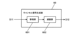
図2は、キャンセル信号生成部60の回路構成の一例を示す図である。キャンセル信号生成部60は、移相部601と、減衰部602とを備えて構成される。
FIG. 2 is a diagram illustrating an example of a circuit configuration of the cancel
移相部601は、遅延器等により構成される移相回路であり、発生信号S11の位相を180度移相した後、減衰部602に出力する。尚、移相の対象とする周波数は、GPS衛星信号と同一の周波数である。
The
減衰部602は、移相部601から出力された信号を所定の減衰率(ゲイン)で減衰させる減衰器であり、減衰させた信号をキャンセル信号S12として加算部50に出力する。
The
減衰部602の減衰率は、GPS受信部と携帯用電子回路との位置関係が確定した後の携帯型電話機1の製造段階で設定される。具体的には、加算部50により加算された後の信号のうち、GPS衛星信号の中間周波数に対応する帯域のノイズ成分の量が最低となるように減衰率が調整され、その調整結果の値が設計値として設定される。
The attenuation rate of the
局部発振信号生成部70は、LO(Local Oscillator)等の発振器で構成されるRF信号乗算用の局部発振信号を生成する回路部であり、生成した局部発振信号を乗算部80に出力する。
The local oscillation
乗算部80は、加算部50による加算結果の信号S3に、局部発振信号生成部70で生成された局部発振信号を乗算することで、RF信号を中間周波数の信号(以下、「IF信号」と称す。)にダウンコンバートし、増幅部90に出力する。
The
増幅部90は、乗算部80から出力されたIF信号を所定の増幅率で増幅する増幅器であり、増幅した信号をフィルタ100に出力する。
The
フィルタ100は、増幅部90で増幅された信号のうち、IF信号の信号成分の周波数帯を含む所定の周波数帯域成分を通過させる帯域通過フィルタであり、通過させた信号S4をA/D変換部110に出力する。
The
A/D変換部110は、アナログ信号をデジタル信号に変換するA/D変換器であり、フィルタ100を通過した信号をデジタル信号に変換した後、ベースバンド処理回路部120に出力する。
The A /
ベースバンド処理回路部120は、RF受信回路部20から出力されたIF信号に対して相関検出処理等を行ってGPS衛星信号を捕捉・抽出し、データを復号して航法メッセージや時刻情報等を取り出し、疑似距離の演算や測位演算等を行う回路部である。尚、GPS衛星信号は、C/Aコード(Coarse and Acquisition)と呼ばれるスペクトラム拡散変調された信号である。
The baseband
携帯用アンテナ130は、携帯型電話機の通信サービス事業者が設置した無線基地局との間で携帯用無線信号の送受信を行うアンテナである。
The
携帯用無線通信回路部140は、RF変換回路、ベースバンド処理回路等によって構成される携帯電話の通信回路部であり、携帯用無線信号の変調・復調等を行うことで、通話やメールの送受信等を実現する。
The portable wireless
ホストCPU150は、ROM180に記憶されているシステムプログラム等の各種プログラムに従って携帯型電話機1の各部を統括的に制御するプロセッサであり、主に電話機としての機能を司る他、ベースバンド処理回路部120において測位された携帯型電話機1の現在位置をプロットしたナビゲーション画面を表示部170に表示させる。
The
操作部160は、操作キーやボタンスイッチ等により構成される入力装置であり、これらの押下信号をホストCPU150に出力する。この操作部160の操作により、通話要求や、ナビゲーション画面の表示要求等の各種指示入力がなされる。
The
表示部170は、LCD(Liquid Crystal Display)等により構成され、ホストCPU150から入力される表示信号に基づいた各種表示を行う表示装置である。表示部170には、日付及び時刻の情報や、ナビゲーション画面等が表示される。
The
ROM180は、読み出し専用の記憶装置であり、携帯型電話機1を統括的に制御するためのシステムプログラムや、通話やメールの送受信を実現するためのプログラム、ナビゲーション機能を実現するためのプログラム等の各種プログラムやデータを記憶している。ホストCPU150は、これらのプログラムやデータに従って処理を実行する。
The
RAM190は、読み書き可能な記憶装置であり、ホストCPU150により実行されるシステムプログラム、各種処理プログラム、各種処理の処理中データ、処理結果等を一時的に記憶するワークエリアを形成している。
The
1−2.原理・動作
図3は、妨害波除去の原理を説明するための図である。図3では、横軸を周波数(f)、縦軸を信号レベル(P)とし、図1の信号S1,S2,S3,S4,S11,S12の周波数スペクトルを模式的に示している。但し、信号S2,S3,S4,S12については、本実施形態の特徴を簡明に説明するため、GPS衛星信号のインバンドIB近傍の領域Rの周波数スペクトルを拡大した図を示している。
1-2. Principle / Operation FIG. 3 is a diagram for explaining the principle of interference wave removal. In FIG. 3, the horizontal axis represents the frequency (f) and the vertical axis represents the signal level (P), and the frequency spectra of the signals S1, S2, S3, S4, S11, and S12 of FIG. However, for the signals S2, S3, S4, and S12, in order to explain the features of this embodiment in a simplified manner, a diagram in which the frequency spectrum of the region R in the vicinity of the inband IB of the GPS satellite signal is enlarged is shown.
GPSアンテナ10からRF受信回路部20に出力される信号S1は、GPS衛星信号に種々のノイズが重畳した信号である。しかし、ノイズの多くは、RF受信回路部20の近傍位置に配置されている携帯用電子回路からGPS受信部側に回り込んだ携帯用無線信号である。GPS衛星信号の周波数スペクトルを「SG」、携帯用無線信号の周波数スペクトルを「SC」として、信号S1,S2の図に図示する。
The signal S1 output from the
GPS衛星信号は、1.57542[GHz](以下、「GPS周波数」と称す。)の搬送波(キャリア)が拡散された1.5[GHz]帯の信号である。このGPS衛星信号は、強度の弱い信号であり、その周波数スペクトル「SG」は、GPS周波数「fG」を中心とする所定帯域をインバンドIBとする。 The GPS satellite signal is a signal in a 1.5 [GHz] band in which a carrier wave of 1.57542 [GHz] (hereinafter referred to as “GPS frequency”) is spread. This GPS satellite signal is a weak signal, and the frequency spectrum “S G ” has a predetermined band centered on the GPS frequency “f G ” as an in-band IB.
一方、携帯用無線信号の周波数は、通信方式にもよるが、1.7[GHz],2.0[GHz]等である。この携帯用無線信号は、GPS衛星信号に対して強度の強い信号であり、その周波数スペクトル「SC」は、例えば携帯用周波数「fC(>fG)」に最大ピーク「MP」を有し、その近傍に複数の局所ピーク「LP」を有する。 On the other hand, the frequency of the portable radio signal is 1.7 [GHz], 2.0 [GHz], etc., depending on the communication method. This portable radio signal is a signal having a stronger intensity than the GPS satellite signal, and its frequency spectrum “S C ” has a maximum peak “MP” at the portable frequency “f C (> f G )”, for example. However, there are a plurality of local peaks “LP” in the vicinity thereof.
以下の説明では、携帯用無線信号の周波数スペクトル「SC」において、最大ピーク「MP」に対応する周波数帯を「メインローブ」、それ以外の周波数帯を「サイドローブ」と称する。 In the following description, in the frequency spectrum “S C ” of the portable radio signal, the frequency band corresponding to the maximum peak “MP” is referred to as “main lobe”, and the other frequency bands are referred to as “side lobes”.
携帯用無線信号は、スペクトラム拡散変調により搬送波(キャリア)が広帯域に拡散されており、その周波数スペクトル「SC」は広がりを持っている。このため、携帯用無線信号のサイドローブの信号が、受信したGPS衛星信号のインバンドIBにおける妨害波となる。 In the portable radio signal, a carrier wave (carrier) is spread over a wide band by spread spectrum modulation, and the frequency spectrum “S C ” has a wide range. For this reason, the sidelobe signal of the portable radio signal becomes an interference wave in the in-band IB of the received GPS satellite signal.
GPSアンテナ10からRF受信回路部20に信号S1が出力されると、SAWフィルタ30は、当該信号S1のうち、GPS衛星信号のインバンドIBを中心とする一定帯域の信号を通過させる。即ち、大概的ではあるが、SAWフィルタ30によって、概ねインバンドIBを中心とする信号が抽出されることとなり、携帯用無線信号のメインローブの信号と、サイドローブの一部の信号とが減衰・除去される。そして、LNA40は、SAWフィルタ30を通過した信号S2を増幅した後、加算部50に出力する。
When the signal S1 is output from the
一方、携帯用電子回路からキャンセル信号生成部60に入力される発生信号S11の周波数スペクトルは、信号S1中に重畳されている携帯用無線信号の成分と同一であり、信号S1の図中の周波数スペクトル「SC」と同一形状で表される。キャンセル信号生成部60は、入力した発生信号S11を移相部601で180度移相した後、減衰部602で減衰させ、キャンセル信号S12として加算部50に出力する。
On the other hand, the frequency spectrum of the generated signal S11 input from the portable electronic circuit to the cancel
ここで、移相部601は、GPS周波数「fG」を移相対象の周波数とするように設計されているため、発生信号S11のうちのインバンドIBの信号成分を180度移相することになる。
Here, since the
その後、加算部50は、LNA40で増幅された信号に、キャンセル信号生成部60で生成されたキャンセル信号S12を加算し、信号S3として乗算部80に出力する。信号S3の周波数スペクトルは、GPS衛星信号のインバンドIBの部分の信号レベルが減少した形状となる。
Thereafter, the
これは、インバンドIBにおいて、キャンセル信号S12が信号S2と逆位相になっており、加算によって信号S2と相殺されたことによるものである。これにより、インバンドにおいて信号S1に重畳していた携帯用無線信号の妨害波が除去されたことになる。 This is because in the in-band IB, the cancel signal S12 has an opposite phase to the signal S2, and is canceled out with the signal S2 by addition. Thereby, the interference wave of the portable radio signal superimposed on the signal S1 in-band is removed.
その後、乗算部80は、加算部50から出力された信号S3に、局部発振信号生成部70で生成された局部発振信号を乗算することで、信号S3をダウンコンバートしてIF信号とし、増幅部90に出力する。
Thereafter, the
そして、増幅部90は、乗算部80から出力された信号を増幅した後、フィルタ100に出力する。フィルタ100は、増幅部90で増幅された信号のうち、GPS衛星信号の中間周波数に対応する帯域(インバンドIBに対応する中間周波数の帯域)の信号を通過させ、信号S4としてA/D変換部110に出力する。
The
信号S4は、アウトバンドの信号がフィルタ100によって遮断された信号である。尚、信号S4はIF信号であるため、周波数スペクトルを全体的に低域側にシフトさせ、IF信号の中心周波数「IFG」、即ちインバンドIBの中心周波数を縦軸として図示している。
The signal S4 is a signal obtained by blocking the out-band signal by the
1−3.作用効果
第1実施形態によれば、GPSアンテナ10で受信された信号がLNA40において増幅された後、加算部50において、キャンセル信号生成部60で生成されたキャンセル信号と加算されることで、受信信号に重畳されたインバンドのノイズがキャンセルされる。
1-3. According to the first embodiment, the signal received by the
受信信号がLNA40で増幅され、信号レベルが引き上げられた後にキャンセル信号と加算されるため、GPSアンテナ10の直後でキャンセル信号を加算する場合に比べて、キャンセル信号の信号レベルの調整を簡単に行うことができ、過度のキャンセル信号によって妨害波成分が増加することを防止することができる。
Since the received signal is amplified by the
2.第2実施形態
2−1.構成
図4は、第2実施形態における携帯型電話機2の機能構成を示すブロック図である。尚、携帯型電話機1と同一の構成要素については同一の符号を付して、説明を省略する。携帯型電話機2は、GPSアンテナ10と、RF受信回路部22と、ベースバンド処理回路部120と、携帯用アンテナ130と、携帯用無線通信回路部140と、ホストCPU150と、操作部160と、表示部170と、ROM180と、RAM190とを備えて構成される。
2. Second Embodiment 2-1. Configuration FIG. 4 is a block diagram showing a functional configuration of the
RF受信回路部22は、SAWフィルタ30と、LNA40と、乗算部82と、加算部52と、キャンセル信号生成部62と、局部発振信号生成部70と、増幅部90と、フィルタ100と、A/D変換部110とを備えて構成される。
The RF
RF受信回路部22が携帯型電話機1のRF受信回路部20と大きく異なる点は、受信信号が乗算部82においてIF信号にダウンコンバートされた後に、加算部52において、キャンセル信号生成部62で生成されたキャンセル信号と加算される点である。従って、キャンセル信号生成部62で生成されるキャンセル信号もまた中間周波数の信号である。
The RF
図5は、キャンセル信号生成部62の回路構成の一例を示す図である。キャンセル信号生成部62は、局部発振信号移相部621と、乗算部622と、減衰部623とを備えて構成される。
FIG. 5 is a diagram illustrating an example of a circuit configuration of the cancel
局部発振信号移相部621は、局部発振信号生成部70から入力された局部発振信号S41を180度移相する移相回路であり、直流信号乗算部6211と、同相信号増幅部6212と、遅延器6213と、直流信号乗算部6214と、直交信号増幅部6215と、加算部6216とを備えて構成される。この局部発振信号移相部621は、直交変調器を用いて局部発振信号の移相器を構成したものであるが、他の構成としてもよいことは勿論である。
The local oscillation signal
直流信号乗算部6211は、所定の電圧を分圧等することにより生成された直流(DC)信号を局部発振信号S41に乗算する乗算器であり、乗算結果の信号を局部発振信号の同相信号(I信号)として、同相信号増幅部6212に出力する。
The direct
同相信号増幅部6212は、直流信号乗算部6211から出力された同相信号を所定の増幅率で増幅する増幅器であり、増幅した信号を加算部6216に出力する。
The in-phase
遅延器6213は、局部発振信号S41の位相を90度遅延させる遅延器であり、遅延させた信号を直流信号乗算部6214に出力する。
The
直流信号乗算部6214は、遅延器6213から出力された信号に、所定の電圧を分圧等することにより生成された直流信号を乗算する乗算器であり、乗算結果の信号を局部発振信号の直交信号(Q信号)として、直交信号増幅部6215に出力する。
The
直交信号増幅部6215は、直交信号乗算部6214から出力された直交信号を所定の増幅率で増幅する増幅器であり、増幅した信号を加算部6216に出力する。
The quadrature
加算部6216は、同相信号増幅部6212で増幅された同相信号と、直交信号増幅部6215で増幅された直交信号とを加算する加算器であり、加算結果の信号を乗算部622に出力する。
The
乗算部622は、携帯用電子回路からの発生信号S31に、発振信号移相部621において移相された局部発振信号を乗算する乗算器であり、乗算結果の信号を減衰部623に出力する。
The
ここで、同相信号増幅部6212及び直交信号増幅部6215のゲインをそれぞれ「−1」とすることで、加算部6216から出力される信号は、180度移相された局部発振信号となる。従って、乗算部622において、180度移相された局部発振信号と乗算されることで、発生信号S31は、180度移相された中間周波数の信号となる。
Here, by setting the gains of the in-phase
減衰部623は、乗算部622によって中間周波数に変換された発生信号S31を所定の減衰率で減衰させる減衰器であり、減衰させた信号をキャンセル信号S32として、加算部52に出力する。減衰部623の減衰率は、加算部52により加算された後の信号のうち、GPS衛星信号の中間周波数に対応する帯域のノイズ成分の量が最低となるような値に製造時に予め設定される。
The attenuating
2−2.原理・動作
図6は、第2実施形態における妨害波除去の原理を説明するための図である。図6では、横軸を周波数(f)、縦軸を信号レベル(P)とし、図4の信号S21,S22,S23,S24,S31,S32の周波数スペクトルを模式的に示している。但し、信号S22,S23,S24,S32の周波数スペクトルについては、本実施形態の特徴を簡明に説明するため、GPS衛星信号のインバンドIBの近傍の領域Rを拡大したものを示している。
2-2. Principle / Operation FIG. 6 is a diagram for explaining the principle of interference wave removal in the second embodiment. In FIG. 6, the frequency (f) is plotted on the horizontal axis and the signal level (P) is plotted on the vertical axis, and the frequency spectra of the signals S21, S22, S23, S24, S31, and S32 in FIG. However, the frequency spectrums of the signals S22, S23, S24, and S32 show an enlarged region R in the vicinity of the in-band IB of the GPS satellite signal in order to briefly explain the feature of the present embodiment.
信号S21は、GPSアンテナ10からRF受信回路部22に出力される信号であり、信号S21に重畳されているノイズの多くは携帯用無線信号である。尚、この信号S21の周波数スペクトルは、図3の信号S1の周波数スペクトルと同一である。
The signal S21 is a signal output from the
信号S21は、SAWフィルタ30を通過することで、携帯用無線信号のメインローブの信号を中心とした所定帯域の信号が抽出される。その後、SAWフィルタ30を通過した信号は、LNA40において増幅された後、乗算部82において局部発振信号と乗算されることでダウンコンバートされ、信号S22として加算部52に出力される。尚、信号S22はIF信号であるため、周波数スペクトルを全体的に低域側にシフトさせ、IF信号の中心周波数「IFG」、即ちインバンドIBの中心周波数を縦軸として図示している。
By passing the signal S21 through the
一方、キャンセル信号生成部62に入力される発生信号S31の周波数スペクトルは、信号S21中に重畳されている携帯用無線信号の成分と同一であり、信号S21の図中の周波数スペクトル「SC」と同一の形状で表される。発生信号S31は、キャンセル信号生成部62の乗算部622において、局部発振信号移相部621から出力された信号と乗算されることで、180度移相されるとともに、ダウンコンバートされて中間周波数の信号となる。
On the other hand, the frequency spectrum of the generated signal S31 input to the cancel
但し、発生信号S31に乗算した信号は、局部発振信号の位相を180度移相した信号であるため、乗算後の信号も、局部発振信号の位相から180度ずれた位相となる。そして、中間周波数に変換された発生信号S31は、減衰部623において減衰されてキャンセル信号S32となり、加算部52に出力される。
However, since the signal multiplied by the generated signal S31 is a signal obtained by shifting the phase of the local oscillation signal by 180 degrees, the multiplied signal also has a phase shifted by 180 degrees from the phase of the local oscillation signal. Then, the generated signal S31 converted to the intermediate frequency is attenuated by the attenuating
加算部52において、受信信号の中間周波数の信号である信号S22にキャンセル信号S32が加算される。この際、信号S22とキャンセル信号S32とは、位相が180度異なる。なぜならば、発生信号S31に乗算された信号は、受信信号に乗算された局部発振信号に対して180度位相が異なる信号だからである。この結果、インバンドIBにおいて、信号S21に重畳していた携帯用無線信号の妨害波が除去されたものとなる。
In the
そして、増幅部90で増幅された信号は、フィルタ100を通過して信号S24となる。信号S24は、アウトバンドの信号がフィルタ100によって遮断された信号である。
Then, the signal amplified by the
2−3.作用効果
第2実施形態によれば、GPSアンテナ10で受信された信号が、乗算部82において局部発振信号と乗算されることでIF信号にダウンコンバートされた後、加算部52において、キャンセル信号生成部62で生成されたキャンセル信号と加算されることで、受信信号に重畳されたインバンドのノイズがキャンセルされる。
2-3. According to the second embodiment, the signal received by the
加算部52において加算されるキャンセル信号は、携帯用電子回路からの発生信号と、局部発振信号生成部70で生成された局部発振信号とに基づいて生成される。具体的には、携帯用電子回路からの発生信号が、180度移相された局部発振信号と乗算されて中間周波数の信号となり、所定の減衰率で減衰されて、キャンセル信号として加算部52に出力される。
The cancel signal added in the adding
携帯用電子回路からの発生信号には、様々な周波数の信号が含まれており、信号レベルも一定ではない。一方、局部発振信号の周波数は一定であり、信号レベルも一定であることから、移相を行うことは容易である。このため、移相した局部発振信号を乗算する構成により、携帯用電子回路からの発生信号の移相を簡易に実現することができる。 The generated signal from the portable electronic circuit includes signals of various frequencies, and the signal level is not constant. On the other hand, since the frequency of the local oscillation signal is constant and the signal level is also constant, phase shifting is easy. For this reason, the phase of the generated signal from the portable electronic circuit can be easily realized by multiplying the phase-shifted local oscillation signal.
3.第3実施形態
3−1.構成
図7は、第3実施形態における携帯型電話機3の機能構成を示すブロック図である。尚、携帯型電話機1と同一の構成要素については同一の符号を付して、説明を省略する。携帯型電話機3は、GPSアンテナ10と、RF受信回路部24と、ベースバンド処理回路部120と、携帯用アンテナ130と、携帯用無線通信回路部140と、ホストCPU150と、操作部160と、表示部170と、ROM180と、RAM190と、無線アンテナ200と、無線通信回路部210とを備えて構成される。
3. Third Embodiment 3-1. Configuration FIG. 7 is a block diagram showing a functional configuration of the
RF受信回路部24は、SAWフィルタ30と、LNA40と、乗算部84と、第1加算部54と、第2加算部56と、第1キャンセル信号生成部64と、第2キャンセル信号生成部66と、局部発振信号生成部70と、増幅部90と、フィルタ100と、A/D変換部110とを備えて構成される。
The RF
無線通信回路部210は、無線アンテナ200を介して、例えばBluetooth(登録商標)やIEEE802.11によるワイヤレスLAN等の通信規格に則った無線通信を他機との間で行う回路部である。
The wireless
携帯型電話機3には、携帯用アンテナ130及び携帯用無線通信回路部140でなる携帯用電子回路と、無線アンテナ200及び無線通信回路部210でなる無線通信用電子回路との2つの電子回路が内蔵される関係上、この2つの電子回路とGPS受信部とは互いに近傍する位置となり、GPS受信部が受信するGPS衛星信号(受信信号)に対する妨害波の発生源が2つ存在する。
The
そこで、携帯用電子回路からの発生信号を打ち消すキャンセル信号を生成する第1キャンセル信号生成部64と、無線通信用電子回路からの発生信号を打ち消すキャンセル信号を生成する第2キャンセル信号生成部66とを設け、生成したキャンセル信号を、第1加算部54及び第2加算部56において、それぞれダウンコンバート後の中間周波数の信号に加算することで、受信信号に重畳される各々の電子回路からのインバンドの妨害波をキャンセル可能に構成している。尚、第1キャンセル信号生成部64及び第2キャンセル信号生成部66の回路構成は、携帯型電話機2のキャンセル信号生成部62の回路構成と同一である。
Therefore, a first cancel
3−2.作用効果
第3実施形態によれば、携帯電話用の電子回路からの発生信号と、無線通信用の電子回路からの発生信号とのそれぞれを打ち消すためのキャンセル信号が、第1キャンセル信号生成部64及び第2キャンセル信号生成部66において生成され、第1加算部54及び第2加算部56において受信信号とそれぞれ加算されることで、受信信号に重畳されたインバンドのノイズがキャンセルされる。従って、複数のノイズの発生源が筐体内に存在する場合であっても、受信信号に重畳されたノイズを適切にキャンセルすることが可能となる。
3-2. Effects According to the third embodiment, the cancel signal for canceling each of the generated signal from the electronic circuit for mobile phone and the generated signal from the electronic circuit for wireless communication is the first cancel
4.変形例
4−1.適用例
本発明は、携帯型電話機の他、携帯型のナビゲーション装置やカーナビゲーション装置、パーソナル・コンピュータ(PC)等の各種電子機器に適用することが可能である。即ち、無線信号を受信する受信回路と、当該受信信号にとっての妨害波(ノイズ)となる信号を発生する電子回路とを備えた電子機器であれば適用可能である。
4). Modified example 4-1. Application Example The present invention can be applied to various electronic devices such as a portable navigation device, a car navigation device, and a personal computer (PC) in addition to the portable phone. In other words, any electronic device including a receiving circuit that receives a radio signal and an electronic circuit that generates a signal that becomes an interference wave (noise) for the received signal is applicable.
受信回路としては、GPS信号受信回路の他、他の各種の通信回路等であってもよい。また、受信回路の受信信号に対する妨害波を発生する電子回路としては、コンピュータシステムや各種の通信回路等であってよい。 The receiving circuit may be other various communication circuits in addition to the GPS signal receiving circuit. Further, the electronic circuit that generates the interference wave with respect to the reception signal of the reception circuit may be a computer system, various communication circuits, or the like.
4−2.衛星測位システム
上述した実施例では、衛星測位システムとしてGPSを一例として説明したが、WAAS、QZSS、GLONASS、GALILEO等の衛星測位システムに適用することが可能である。
4-2. Satellite positioning system In the above-described embodiments, the GPS has been described as an example of the satellite positioning system. However, the present invention can be applied to satellite positioning systems such as WAAS, QZSS, GLONASS, and GALILEO.
4−3.減衰部
キャンセル信号生成部が、加算部によって加算された後の信号に基づいて減衰部の減衰率を調整するようにしてもよい。これは、GPS受信部近傍に設置される電子回路は常時一定の回路動作をしているとは限らず、動作時/停止時等に応じて回路動作を適宜変化させることが予想されるからである。
4-3. Attenuator The cancel signal generator may adjust the attenuation factor of the attenuator based on the signal added by the adder. This is because the electronic circuit installed in the vicinity of the GPS receiving unit does not always perform a constant circuit operation, and it is expected that the circuit operation is appropriately changed according to the operation time / stopping time. is there.
具体的には、例えば、フィルタ100の出力信号を減衰部に入力して、フィルタ100を通過したノイズキャンセル後の信号が減衰部にフィードバックされるように構成する。そして、減衰部は、当該フィードバック信号に基づいて減衰率を調整する。
Specifically, for example, the output signal of the
図8は、この場合における減衰部の回路構成の一例を示す図である。減衰部は、減衰器と、信号レベル検出部と、差動増幅部とを備えて構成される。 FIG. 8 is a diagram illustrating an example of a circuit configuration of the attenuation unit in this case. The attenuating unit includes an attenuator, a signal level detecting unit, and a differential amplifying unit.
減衰器は、入力信号を差動増幅部から出力された減衰率の制御信号(以下、「ゲイン制御信号」と称す。)に応じた減衰率で減衰させる可変減衰器であり、減衰させた信号をキャンセル信号として加算部に出力する。 The attenuator is a variable attenuator that attenuates an input signal at an attenuation rate according to an attenuation rate control signal (hereinafter referred to as a “gain control signal”) output from the differential amplification unit. Is output to the adder as a cancel signal.
信号レベル検出部は、公知の信号レベル検出回路により構成される回路部であり、フィードバック信号の信号レベルを検出して差動増幅部に出力する。 The signal level detection unit is a circuit unit configured by a known signal level detection circuit, detects the signal level of the feedback signal, and outputs it to the differential amplification unit.
差動増幅部は、オペアンプ等により構成される公知の差動増幅回路であり、信号レベル検出部で検出された信号の信号レベルと、基準信号の信号レベルとを比較し、その差分に応じた信号をゲイン制御信号として減衰器に出力する。尚、基準信号は、所定電圧を分圧する等して生成される。 The differential amplifying unit is a known differential amplifying circuit configured by an operational amplifier or the like, compares the signal level of the signal detected by the signal level detecting unit with the signal level of the reference signal, and according to the difference The signal is output to the attenuator as a gain control signal. The reference signal is generated by dividing a predetermined voltage.
かかる構成により、ノイズキャンセルの結果をフィードバックして減衰率を調整することができ、電子回路からの発生信号の信号レベルが変化したとしても、随時適切な信号レベルのキャンセル信号を生成することができる。尚、この減衰部の回路構成は、上述した全ての実施形態におけるキャンセル信号生成部に適用することが可能である。 With this configuration, the attenuation rate can be adjusted by feeding back the result of noise cancellation, and even if the signal level of the signal generated from the electronic circuit changes, a cancel signal with an appropriate signal level can be generated as needed. . The circuit configuration of the attenuation unit can be applied to the cancel signal generation unit in all the embodiments described above.
4−4.RF受信回路部
第3実施形態で説明した携帯型電話機3のRF受信回路部24の構成を、第1実施形態で説明した携帯型電話機1のRF受信回路部20の構成に置き換えてもよい。具体的には、携帯電話用の通信回路と、無線通信用の通信回路とのそれぞれに対応するキャンセル信号生成部60を設ける。そして、受信信号をLNA40において増幅した後に、加算部50において、各々のキャンセル信号生成部60で生成されたキャンセル信号を受信信号に加算し、加算結果の信号に対して乗算部80でのダウンコンバートを行うようにする。
4-4. RF Receiver Circuit Unit The configuration of the RF
1 携帯型電話機、 10 GPSアンテナ、 20 RF受信回路部、
30 SAWフィルタ、 40 LNA、 50 加算部、
60 キャンセル信号生成部、 70 局部発振信号生成部、 80 乗算部、
90 増幅部、 100 フィルタ、 110 A/D変換部、
120 ベースバンド処理回路部、 130 携帯用アンテナ、
140 携帯用無線通信回路部、 150 ホストCPU、 160 操作部、
170 表示部、 180 ROM、 190 RAM
1 mobile phone, 10 GPS antenna, 20 RF receiving circuit,
30 SAW filters, 40 LNA, 50 adder,
60 cancel signal generator, 70 local oscillation signal generator, 80 multiplier,
90 amplification unit, 100 filter, 110 A / D conversion unit,
120 baseband processing circuit unit, 130 portable antenna,
140 portable wireless communication circuit unit, 150 host CPU, 160 operation unit,
170 display unit, 180 ROM, 190 RAM
Claims (10)
局部発振信号を生成する局部発振信号生成部と、
前記局部発振信号を用いて、前記受信部により受信された受信信号を中間周波数の信号に変換する中間周波変換部と、
前記局部発振信号を180度移相した信号と、前記受信部近傍の電子回路からの発生信号とを乗算してキャンセル信号を生成するキャンセル信号生成部と、
前記中間周波変換部から出力される信号に前記キャンセル信号を加算する加算部と、
を備えた受信回路。 A receiver for receiving a radio signal;
A local oscillation signal generator for generating a local oscillation signal;
Using the local oscillation signal, an intermediate frequency conversion unit that converts a reception signal received by the reception unit into an intermediate frequency signal;
A cancellation signal generation unit that generates a cancellation signal by multiplying a signal obtained by phase-shifting the local oscillation signal by 180 degrees and a generation signal from an electronic circuit in the vicinity of the reception unit;
An adder for adding the cancel signal to a signal output from the intermediate frequency converter ;
Receiving circuit.
前記加算部は、前記受信部により受信された受信信号の信号処理系統の途中所定位置であって前記フィルタ部の前で、前記中間周波変換部から出力される中間周波数の信号に前記キャンセル信号を加算する、
請求項1に記載の受信回路。 Among the signals output from the intermediate frequency conversion unit , further comprising a filter unit that passes a band corresponding to the intermediate frequency of the radio signal,
The addition unit, before a middle position of the signal processing system of a reception signal received by the receiving portion of the filter unit, the cancellation signal to the intermediate frequency signal output from said intermediate frequency conversion section to add,
The receiving circuit according to claim 1.
前記フィルタ部から出力される信号の信号レベルに基づき、前記減衰部の減衰率を制御する制御信号を生成して出力する減衰率制御部を備え、
前記減衰部は、前記減衰率制御部から出力される前記制御信号に応じた減衰率で前記移相部により移相された信号を減衰させる、
請求項2に記載の受信回路。 The cancellation signal generation unit includes an attenuation unit that attenuates the multiplied signal with a predetermined attenuation rate,
An attenuation rate control unit that generates and outputs a control signal for controlling the attenuation rate of the attenuation unit based on the signal level of the signal output from the filter unit;
The attenuation unit attenuates the signal phase-shifted by the phase-shifting unit at an attenuation rate according to the control signal output from the attenuation rate control unit;
The receiving circuit according to claim 2 .
前記加算部は、前記各キャンセル信号生成部それぞれにより生成されたキャンセル信号を加算する、
請求項1〜5の何れか一項に記載の受信回路。 For each electronic circuit arranged in the vicinity of the receiving unit that receives the radio signal, the cancel signal generating unit that generates a cancel signal that cancels the generated signal from the corresponding electronic circuit,
The adding unit adds the cancel signals generated by the cancel signal generating units.
The receiving circuit as described in any one of Claims 1-5.
前記無線通信回路は携帯電話用の通信回路である、
携帯型電話機である請求項8に記載の電子機器。 The receiving circuit is a circuit for receiving a GPS satellite signal;
The wireless communication circuit is a communication circuit for a mobile phone,
The electronic device according to claim 8, which is a mobile phone.
前記局部発振信号を180度移相した信号と、前記受信部近傍の電子回路からの発生信号とを乗算してキャンセル信号を生成することと、
前記変換された信号に前記キャンセル信号を加算することと、
を含むノイズキャンセル方法。 Using a local oscillation signal, converting a reception signal of a reception unit that receives a radio signal into a signal of an intermediate frequency;
Multiplying a signal obtained by shifting the local oscillation signal by 180 degrees and a generated signal from an electronic circuit in the vicinity of the receiving unit to generate a cancellation signal;
Adding the cancellation signal to the converted signal;
Including noise cancellation method.
Priority Applications (6)
| Application Number | Priority Date | Filing Date | Title |
|---|---|---|---|
| JP2006335454A JP4984869B2 (en) | 2006-12-13 | 2006-12-13 | Reception circuit, electronic device, and noise canceling method |
| US11/953,614 US7979029B2 (en) | 2006-12-13 | 2007-12-10 | Receiver circuit, electronic instrument, and signal processing method |
| EP07024144A EP1933162B1 (en) | 2006-12-13 | 2007-12-12 | Receiver circuit, electronic instrument, and signal processing method |
| CN2007101987379A CN101202558B (en) | 2006-12-13 | 2007-12-12 | Receiver circuit, electronic instrument, and signal processing method |
| KR1020070129893A KR20080055696A (en) | 2006-12-13 | 2007-12-13 | Receiver circuit, electronic instrument, and signal processing method |
| US13/154,001 US8340583B2 (en) | 2006-12-13 | 2011-06-06 | Receiver circuit, electronic instrument, and signal processing method |
Applications Claiming Priority (1)
| Application Number | Priority Date | Filing Date | Title |
|---|---|---|---|
| JP2006335454A JP4984869B2 (en) | 2006-12-13 | 2006-12-13 | Reception circuit, electronic device, and noise canceling method |
Publications (3)
| Publication Number | Publication Date |
|---|---|
| JP2008148187A JP2008148187A (en) | 2008-06-26 |
| JP2008148187A5 JP2008148187A5 (en) | 2010-02-04 |
| JP4984869B2 true JP4984869B2 (en) | 2012-07-25 |
Family
ID=39256868
Family Applications (1)
| Application Number | Title | Priority Date | Filing Date |
|---|---|---|---|
| JP2006335454A Expired - Fee Related JP4984869B2 (en) | 2006-12-13 | 2006-12-13 | Reception circuit, electronic device, and noise canceling method |
Country Status (5)
| Country | Link |
|---|---|
| US (2) | US7979029B2 (en) |
| EP (1) | EP1933162B1 (en) |
| JP (1) | JP4984869B2 (en) |
| KR (1) | KR20080055696A (en) |
| CN (1) | CN101202558B (en) |
Families Citing this family (6)
| Publication number | Priority date | Publication date | Assignee | Title |
|---|---|---|---|---|
| CN101968540A (en) * | 2010-09-15 | 2011-02-09 | 中兴通讯股份有限公司 | Method and device for processing satellite positioning signal and mobile terminal |
| WO2013078680A1 (en) * | 2011-12-02 | 2013-06-06 | 华为技术有限公司 | Method for eliminating adjacent channel interference, modem and system |
| US9680415B2 (en) * | 2015-01-23 | 2017-06-13 | Cambium Networks Limited | Apparatus and method for filtering radio frequency signals of transceiver integrated circuits |
| CN104678407B (en) * | 2015-02-16 | 2017-06-20 | 络达科技股份有限公司 | It is used to reduce the device and method that harmonic wave interference gps signal is received |
| CN105049072A (en) * | 2015-06-15 | 2015-11-11 | 成都中微电微波技术有限公司 | Electronic communication apparatus with GPS antenna |
| US9729179B1 (en) | 2016-06-23 | 2017-08-08 | Qualcomm Incorporated | Feed-forward interference cancellation in a receiver |
Family Cites Families (14)
| Publication number | Priority date | Publication date | Assignee | Title |
|---|---|---|---|---|
| US4989262A (en) * | 1988-11-28 | 1991-01-29 | Nec Corporation | Demodulator with multiple interference cancellers responsive to correlations between undesired signals and error signals |
| JPH09153827A (en) * | 1995-11-30 | 1997-06-10 | Nec Eng Ltd | Receiving device |
| JPH1127160A (en) * | 1997-07-04 | 1999-01-29 | Kokusai Electric Co Ltd | Radio information terminal |
| JPH1194888A (en) * | 1997-09-16 | 1999-04-09 | Ricoh Co Ltd | Semiconductor integrated circuit suitable for evaluating radiation noise, and method for evaluating radiation noise using it |
| EP1091497A1 (en) * | 1999-08-24 | 2001-04-11 | Telefonaktiebolaget L M Ericsson (Publ) | Transmitter leakage cancellation circuit for co-located GPS receiver |
| US6961019B1 (en) * | 2000-08-10 | 2005-11-01 | Sirf Technology, Inc. | Method and apparatus for reducing GPS receiver jamming during transmission in a wireless receiver |
| FI113990B (en) * | 2001-04-27 | 2004-07-15 | Nokia Corp | Procedure for reducing interference in a receiver and electronic device |
| US7127211B2 (en) * | 2002-02-21 | 2006-10-24 | Telefonaktiebolaget Lm Ericsson (Publ) | Method and apparatus for reduced intermodulation distortion in a radio transceiver |
| US7043208B2 (en) * | 2002-10-15 | 2006-05-09 | Motorola, Inc. | Method and apparatus to reduce interference in a communication device |
| JP4094444B2 (en) * | 2003-01-31 | 2008-06-04 | 株式会社エヌ・ティ・ティ・ドコモ | Wireless communication terminal |
| US8253624B2 (en) * | 2003-06-02 | 2012-08-28 | Motorola Mobility Llc | Detection and reduction of periodic jamming signals in GPS receivers and methods therefor |
| US7123676B2 (en) | 2003-11-17 | 2006-10-17 | Quellan, Inc. | Method and system for antenna interference cancellation |
| JP4468772B2 (en) * | 2004-09-07 | 2010-05-26 | 富士通株式会社 | Receiver circuit |
| JP2006145315A (en) | 2004-11-18 | 2006-06-08 | Seiko Epson Corp | Positioning apparatus |
-
2006
- 2006-12-13 JP JP2006335454A patent/JP4984869B2/en not_active Expired - Fee Related
-
2007
- 2007-12-10 US US11/953,614 patent/US7979029B2/en not_active Expired - Fee Related
- 2007-12-12 EP EP07024144A patent/EP1933162B1/en not_active Expired - Fee Related
- 2007-12-12 CN CN2007101987379A patent/CN101202558B/en not_active Expired - Fee Related
- 2007-12-13 KR KR1020070129893A patent/KR20080055696A/en not_active Application Discontinuation
-
2011
- 2011-06-06 US US13/154,001 patent/US8340583B2/en not_active Expired - Fee Related
Also Published As
| Publication number | Publication date |
|---|---|
| JP2008148187A (en) | 2008-06-26 |
| US20080143586A1 (en) | 2008-06-19 |
| US20110237215A1 (en) | 2011-09-29 |
| EP1933162A1 (en) | 2008-06-18 |
| US7979029B2 (en) | 2011-07-12 |
| EP1933162B1 (en) | 2013-02-13 |
| CN101202558A (en) | 2008-06-18 |
| CN101202558B (en) | 2011-06-15 |
| KR20080055696A (en) | 2008-06-19 |
| US8340583B2 (en) | 2012-12-25 |
Similar Documents
| Publication | Publication Date | Title |
|---|---|---|
| JP4984879B2 (en) | Reception circuit, noise cancellation circuit, and electronic equipment | |
| US8804791B2 (en) | Communication device, noise removing method, and program | |
| JP4984869B2 (en) | Reception circuit, electronic device, and noise canceling method | |
| JP5908568B2 (en) | Spool damping device, system, and method | |
| US20100085251A1 (en) | Positioning receiver | |
| JP5874929B2 (en) | Receiver | |
| JP5029190B2 (en) | Reception circuit, electronic device, and noise canceling method | |
| JP4973206B2 (en) | POSITIONING DEVICE, ELECTRONIC DEVICE, FILTER PASS BAND VARIABLE METHOD, PROGRAM, AND STORAGE MEDIUM | |
| JP4849025B2 (en) | Reception circuit, electronic device, and noise canceling method | |
| US20080144485A1 (en) | Receiver circuit, electronic instrument, and signal processing method | |
| JP4941237B2 (en) | Mobile communication terminal | |
| US8073408B2 (en) | Semiconductor integrated circuit including a mixer and wireless communication apparatus | |
| JP2009100441A (en) | Noise cancel method, noise cancel type amplifying circuit, and receiving circuit and electronic device including noise cancel type amplifying circuit | |
| JP2008187367A (en) | Reception circuit and electronic equipment | |
| JP2006352772A (en) | Amplifier, radio receiver and signal receiver | |
| US20090080669A1 (en) | Noise cancel method, noise cancel type amplifying circuit, and receiving circuit and electronic device including noise cancel type amplifying circuit | |
| JP2008160690A (en) | Optimal setting search device, optimal setting search method, and program | |
| JP2001102942A (en) | Direct conversion receiver | |
| JP2009049449A (en) | Band-pass filter, receiving system, and electronic device | |
| JP2009033619A (en) | Receiving circuit, electronic equipment, and noise canceling method |
Legal Events
| Date | Code | Title | Description |
|---|---|---|---|
| A521 | Request for written amendment filed |
Free format text: JAPANESE INTERMEDIATE CODE: A523 Effective date: 20091210 |
|
| A621 | Written request for application examination |
Free format text: JAPANESE INTERMEDIATE CODE: A621 Effective date: 20091210 |
|
| A977 | Report on retrieval |
Free format text: JAPANESE INTERMEDIATE CODE: A971007 Effective date: 20120110 |
|
| A131 | Notification of reasons for refusal |
Free format text: JAPANESE INTERMEDIATE CODE: A131 Effective date: 20120117 |
|
| A521 | Request for written amendment filed |
Free format text: JAPANESE INTERMEDIATE CODE: A523 Effective date: 20120315 |
|
| TRDD | Decision of grant or rejection written | ||
| A01 | Written decision to grant a patent or to grant a registration (utility model) |
Free format text: JAPANESE INTERMEDIATE CODE: A01 Effective date: 20120403 |
|
| A01 | Written decision to grant a patent or to grant a registration (utility model) |
Free format text: JAPANESE INTERMEDIATE CODE: A01 |
|
| A61 | First payment of annual fees (during grant procedure) |
Free format text: JAPANESE INTERMEDIATE CODE: A61 Effective date: 20120416 |
|
| R150 | Certificate of patent or registration of utility model |
Free format text: JAPANESE INTERMEDIATE CODE: R150 |
|
| FPAY | Renewal fee payment (event date is renewal date of database) |
Free format text: PAYMENT UNTIL: 20150511 Year of fee payment: 3 |
|
| S531 | Written request for registration of change of domicile |
Free format text: JAPANESE INTERMEDIATE CODE: R313531 |
|
| R350 | Written notification of registration of transfer |
Free format text: JAPANESE INTERMEDIATE CODE: R350 |
|
| LAPS | Cancellation because of no payment of annual fees |