JP4978283B2 - Motor drive control circuit, semiconductor device, electronic timepiece, and electronic timepiece with power generator - Google Patents
Motor drive control circuit, semiconductor device, electronic timepiece, and electronic timepiece with power generator Download PDFInfo
- Publication number
- JP4978283B2 JP4978283B2 JP2007102862A JP2007102862A JP4978283B2 JP 4978283 B2 JP4978283 B2 JP 4978283B2 JP 2007102862 A JP2007102862 A JP 2007102862A JP 2007102862 A JP2007102862 A JP 2007102862A JP 4978283 B2 JP4978283 B2 JP 4978283B2
- Authority
- JP
- Japan
- Prior art keywords
- voltage
- power supply
- circuit
- motor
- control circuit
- Prior art date
- Legal status (The legal status is an assumption and is not a legal conclusion. Google has not performed a legal analysis and makes no representation as to the accuracy of the status listed.)
- Expired - Fee Related
Links
- 239000004065 semiconductor Substances 0.000 title claims description 26
- 230000005669 field effect Effects 0.000 claims description 83
- 238000010248 power generation Methods 0.000 claims description 82
- 230000003071 parasitic effect Effects 0.000 claims description 14
- 238000007599 discharging Methods 0.000 claims description 13
- 238000012545 processing Methods 0.000 claims description 9
- 238000012544 monitoring process Methods 0.000 claims description 3
- 239000003990 capacitor Substances 0.000 description 48
- 238000000034 method Methods 0.000 description 21
- 238000004804 winding Methods 0.000 description 21
- 238000001514 detection method Methods 0.000 description 14
- 230000008569 process Effects 0.000 description 14
- 230000000694 effects Effects 0.000 description 8
- 230000004044 response Effects 0.000 description 8
- 230000008859 change Effects 0.000 description 6
- 238000010586 diagram Methods 0.000 description 6
- 230000007246 mechanism Effects 0.000 description 5
- 230000007423 decrease Effects 0.000 description 4
- 230000010355 oscillation Effects 0.000 description 4
- 230000003247 decreasing effect Effects 0.000 description 3
- 230000004048 modification Effects 0.000 description 3
- 238000012986 modification Methods 0.000 description 3
- 230000003111 delayed effect Effects 0.000 description 2
- 238000009499 grossing Methods 0.000 description 2
- 238000004519 manufacturing process Methods 0.000 description 2
- 238000005070 sampling Methods 0.000 description 2
- NDVLTYZPCACLMA-UHFFFAOYSA-N silver oxide Chemical compound [O-2].[Ag+].[Ag+] NDVLTYZPCACLMA-UHFFFAOYSA-N 0.000 description 2
- HBBGRARXTFLTSG-UHFFFAOYSA-N Lithium ion Chemical compound [Li+] HBBGRARXTFLTSG-UHFFFAOYSA-N 0.000 description 1
- 230000008901 benefit Effects 0.000 description 1
- 238000007796 conventional method Methods 0.000 description 1
- 239000013078 crystal Substances 0.000 description 1
- 230000005685 electric field effect Effects 0.000 description 1
- 230000006698 induction Effects 0.000 description 1
- 239000004973 liquid crystal related substance Substances 0.000 description 1
- 229910001416 lithium ion Inorganic materials 0.000 description 1
- 230000002265 prevention Effects 0.000 description 1
- 229910001923 silver oxide Inorganic materials 0.000 description 1
- 230000006641 stabilisation Effects 0.000 description 1
- 238000011105 stabilization Methods 0.000 description 1
- 239000000758 substrate Substances 0.000 description 1
Images


Classifications
-
- H—ELECTRICITY
- H02—GENERATION; CONVERSION OR DISTRIBUTION OF ELECTRIC POWER
- H02P—CONTROL OR REGULATION OF ELECTRIC MOTORS, ELECTRIC GENERATORS OR DYNAMO-ELECTRIC CONVERTERS; CONTROLLING TRANSFORMERS, REACTORS OR CHOKE COILS
- H02P8/00—Arrangements for controlling dynamo-electric motors rotating step by step
- H02P8/02—Arrangements for controlling dynamo-electric motors rotating step by step specially adapted for single-phase or bi-pole stepper motors, e.g. watch-motors, clock-motors
-
- G—PHYSICS
- G04—HOROLOGY
- G04C—ELECTROMECHANICAL CLOCKS OR WATCHES
- G04C10/00—Arrangements of electric power supplies in time pieces
-
- G—PHYSICS
- G04—HOROLOGY
- G04C—ELECTROMECHANICAL CLOCKS OR WATCHES
- G04C3/00—Electromechanical clocks or watches independent of other time-pieces and in which the movement is maintained by electric means
Landscapes
- Engineering & Computer Science (AREA)
- Power Engineering (AREA)
- Physics & Mathematics (AREA)
- General Physics & Mathematics (AREA)
- Electromechanical Clocks (AREA)
- Control Of Stepping Motors (AREA)
- Control Of Direct Current Motors (AREA)
- Control Of Electric Motors In General (AREA)
- Dc-Dc Converters (AREA)
Description
本発明は、モータ駆動制御回路、このモータ駆動制御回路を備えた半導体装置、電子時計および発電装置付き電子時計に関する。 The present invention relates to a motor drive control circuit, a semiconductor device provided with the motor drive control circuit, an electronic timepiece, and an electronic timepiece with a power generator.
ステッピングモータなどのモータは、各種機器のアクチュエータとして広く利用されている。例えば、電子時計においては、指針を駆動するアクチュエータとして利用されている。
このようなモータには作動電圧範囲があり、モータを安定して駆動するためには、前記作動電圧範囲内においてモータ駆動電圧を一定に維持すること、つまりモータ駆動電圧を定電圧にすることが好ましい。
そして、モータ駆動電源として、従来用いられていた酸化銀等の一次電池は、出力電圧も一定であるため、モータ駆動電圧を定電圧にすることは容易であった。
Motors such as stepping motors are widely used as actuators for various devices. For example, in an electronic timepiece, it is used as an actuator for driving a pointer.
Such a motor has an operating voltage range, and in order to drive the motor stably, maintaining the motor driving voltage constant within the operating voltage range, that is, making the motor driving voltage constant. preferable.
In addition, since a primary battery such as silver oxide that has been conventionally used as a motor driving power source has a constant output voltage, it is easy to set the motor driving voltage to a constant voltage.
一方、近年では、電池交換を不要にするため、回転錘による自動巻き発電装置やソーラー発電装置と、発電装置で発電された電流で充電される二次電池とを設け、二次電池をモータの駆動電源とするものが広く利用されるようになった。
この際、二次電池は充電によって電圧が上昇するため、モータ作動電圧を超えてしまう可能性がある。
On the other hand, in recent years, in order to eliminate the need for battery replacement, a self-winding power generation device or a solar power generation device using a rotating weight, and a secondary battery charged with a current generated by the power generation device are provided, and the secondary battery is installed in the motor. What is used as a drive power supply has come to be widely used.
At this time, since the voltage of the secondary battery increases due to charging, there is a possibility that the motor operating voltage may be exceeded.
このため、モータ駆動電圧を制御する電源部に、3つの降圧用コンデンサと、1つの平滑用コンデンサを搭載した降圧回路を設け、二次電池の電圧を降圧した電圧をモータの駆動回路に供給することで、二次電池の電圧が上昇してもモータ駆動電圧を、モータ作動電圧範囲に調整する駆動制御方法が知られている(例えば特許文献1)。 For this reason, a step-down circuit equipped with three step-down capacitors and one smoothing capacitor is provided in the power supply unit for controlling the motor drive voltage, and a voltage obtained by stepping down the voltage of the secondary battery is supplied to the motor drive circuit. Thus, a drive control method is known in which the motor drive voltage is adjusted to a motor operating voltage range even if the voltage of the secondary battery increases (for example, Patent Document 1).
また、充電による二次電池の電圧上昇を過充電防止機構(リミッタ)で抑制し、モータ駆動電圧が一定電圧値以上にならないように抑制することで、モータ駆動を安定化させる駆動制御方法も知られている(例えば特許文献2)。 Also known is a drive control method that stabilizes the motor drive by suppressing the voltage rise of the secondary battery due to charging with an overcharge prevention mechanism (limiter) so that the motor drive voltage does not exceed a certain voltage value. (For example, Patent Document 2).
しかしながら、特許文献1では次の2つの課題があった。
第1に、降圧回路は二次電池電圧を所定の倍率で小さくするので、充電により二次電池電圧が上昇すると、電源部の降圧電圧も上昇し、モータ駆動電圧が変動して定電圧にならないという問題があった。
すなわち、アナログ的に上昇する二次電池電圧に対応させて降圧電圧を一定にするには、細かい分解能で、多くの降圧倍率が必要となる。しかしながら、このような多くの降圧倍率を設定することは、多数のコンデンサなどが必要となり、回路構成上、困難である。
一方、特許文献1のように、2つの降圧倍率2/3と1/3だけで降圧制御を行う場合には、二次電池電圧がアナログ的に上昇すると、到底、降圧電圧を一定にすることができないという問題があった。
However, Patent Document 1 has the following two problems.
First, since the step-down circuit reduces the secondary battery voltage by a predetermined magnification, when the secondary battery voltage rises due to charging, the step-down voltage of the power supply unit also rises, and the motor drive voltage fluctuates and does not become a constant voltage. There was a problem.
That is, in order to make the step-down voltage constant corresponding to the secondary battery voltage that increases in an analog manner, many step-down magnifications are required with fine resolution. However, setting such many step-down magnifications requires a large number of capacitors and is difficult in terms of circuit configuration.
On the other hand, when performing step-down control with only two step-down magnifications 2/3 and 1/3 as in Patent Document 1, if the secondary battery voltage rises in an analog manner, the step-down voltage must be kept constant. There was a problem that could not.
第2に、電源部がモータの駆動回路に電池電圧を供給している状態から、モータ駆動の条件に応じて、例えば、降圧倍率を2/3に設定し、2/3降圧電圧をモータの駆動回路に供給しようとしても、電源部は平滑用コンデンサを搭載しているため、時定数により、モータ駆動電圧を瞬時に降圧することができないという問題があった。
このため、モータを安定して駆動させるためには、電源部から供給されるモータ駆動電圧が降圧した電圧となるまでの時間以上の待機時間を設定する必要があり、迅速にモータを駆動したい場合においては設定した待機時間中はモータを駆動させることができず、モータ駆動に遅延が発生するという問題があった。
Second, from the state in which the power supply unit supplies the battery voltage to the motor drive circuit, for example, the step-down magnification is set to 2/3 according to the motor drive conditions, and the 2/3 step-down voltage is set to the motor drive circuit. Even if it is going to be supplied to the drive circuit, since the power supply unit has a smoothing capacitor, the motor drive voltage cannot be stepped down instantaneously due to the time constant.
For this reason, in order to drive the motor stably, it is necessary to set a standby time longer than the time until the motor drive voltage supplied from the power supply unit becomes a reduced voltage. However, there is a problem that the motor cannot be driven during the set standby time, and a delay occurs in driving the motor.
また、特許文献2では、モータの作動電圧領域が比較的低い場合は、二次電池電圧が低い領域でリミッタを作動させる必要があり、二次電池の動作持続時間が短くなるという問題があった。すなわち、二次電池は、充電により電池電圧が上昇するため、リミッタの動作電圧が高いほど充電量が多くなり、持続時間も長くなる。つまり、リミッタを動作させる電圧を低くすればするほど、充電電圧が低下し、持続時間も短くなる。
従って、モータの作動電圧領域が低いためにリミッタを低い電圧で作動させると、その分、持続時間が短縮してしまうという問題がある。
Moreover, in patent document 2, when the operating voltage area | region of a motor is comparatively low, it is necessary to operate a limiter in the area | region where a secondary battery voltage is low, and there existed a problem that the operation duration of a secondary battery became short. . That is, since the battery voltage of the secondary battery increases due to charging, the amount of charge increases and the duration increases as the operating voltage of the limiter increases. In other words, the lower the voltage for operating the limiter, the lower the charging voltage and the shorter the duration.
Therefore, since the operating voltage range of the motor is low, there is a problem that if the limiter is operated at a low voltage, the duration is shortened accordingly.
一方で、モータ駆動の安定化と、二次電池の動作持続時間を長くすることを両立させるには、二次電池の電圧が高くなってもモータを駆動できるように、モータの作動電圧範囲を広く確保する必要がある。
しかしながら、作動電圧範囲の広いモータは、通常、性能面等で制約があり、特に高速で正転および逆転動作を行うようなモータでは作動電圧範囲を広く確保することが難しく、利用できるモータが限定されるという問題もあった。
また、モータ駆動を安定化させる為、モータ駆動中のみ二次電池の過充電を防止する方法もあるが、上昇した二次電池電圧でモータ駆動電圧が安定するだけであり、結局、モータの作動電圧範囲は広く確保する必要がある。さらに、モータ駆動中は二次電池への充電ができないため、充電効率が低下するという問題もある。
On the other hand, in order to achieve both stabilization of motor drive and longer operation duration of the secondary battery, the motor operating voltage range should be set so that the motor can be driven even when the secondary battery voltage increases. It is necessary to secure it widely.
However, motors with a wide operating voltage range usually have limitations in terms of performance and the like, and it is difficult to secure a wide operating voltage range with motors that perform forward and reverse operations at high speeds, and the motors that can be used are limited There was also a problem of being.
In addition, there is a method to prevent overcharge of the secondary battery only during motor driving in order to stabilize the motor drive, but the motor drive voltage is only stabilized by the increased secondary battery voltage, and eventually the motor operation It is necessary to ensure a wide voltage range. Furthermore, since the secondary battery cannot be charged while the motor is being driven, there is a problem that the charging efficiency is lowered.
本発明は、モータ駆動時にモータ駆動電圧を迅速にモータ作動電圧範囲内の所定の定電圧にでき、主電源電圧に依存しないモータ駆動電圧をモータ駆動回路に供給して確実にモータを駆動させることができるモータ駆動制御回路、半導体装置および電子時計を提供することを第1の目的とする。
また、発電装置および二次電源を備え、二次電源を主電源としてモータを駆動する際に、二次電源の充電を損なうことなく、かつ、持続時間を長くすることができるとともに、モータ駆動時にモータ駆動電圧を迅速にモータ作動電圧範囲内の所定の定電圧にでき、二次電源の充電による電圧上昇に依存しないモータ駆動電圧をモータ駆動回路に供給して確実にモータを駆動させることができるモータ駆動制御回路、半導体装置および発電装置付き電子時計を提供することを第2の目的とする。
According to the present invention, when a motor is driven, the motor drive voltage can be quickly set to a predetermined constant voltage within the motor operating voltage range, and the motor drive voltage independent of the main power supply voltage is supplied to the motor drive circuit to reliably drive the motor. It is a first object of the present invention to provide a motor drive control circuit, a semiconductor device, and an electronic timepiece that can be used.
In addition, when the motor is driven with the power generation device and the secondary power source, and the secondary power source is used as the main power source, the duration of the secondary power source can be extended without impairing the charging of the secondary power source. The motor drive voltage can be quickly set to a predetermined constant voltage within the motor operating voltage range, and the motor drive voltage can be supplied to the motor drive circuit without depending on the voltage increase due to the charging of the secondary power supply, so that the motor can be driven reliably. A second object is to provide a motor drive control circuit, a semiconductor device, and an electronic timepiece with a power generator.
本発明は、主電源によって作動され、かつ、モータの駆動を制御するモータ駆動制御回路であって、前記モータを駆動する駆動回路と、前記主電源および駆動回路間に設けられて、主電源から供給される電気エネルギを用いて駆動回路へ駆動電圧を供給する電源回路と、前記電源回路から供給される電気エネルギを蓄積する蓄電手段と、前記電源回路の作動を制御する電源制御回路とを備え、前記電源制御回路は、前記駆動回路を、主電源の電圧で駆動する主電源駆動モードと、前記所定の定電圧で駆動する定電圧駆動モードとを選択可能に構成され、主電源駆動モードが選択された場合には、前記電源回路を作動して主電源から駆動回路へ電気エネルギを供給して駆動し、定電圧駆動モードが選択された場合には、前記駆動電圧を監視し、前記駆動電圧が所定の定電圧以上の場合は、前記電源回路を停止して主電源から駆動回路への電気エネルギの供給を停止し、かつ、前記蓄電手段に蓄積された電気エネルギを駆動回路に供給し、前記駆動電圧が所定の定電圧未満の場合は、前記電源回路を作動して主電源から駆動回路に電気エネルギを供給することを特徴とする。 The present invention is a motor drive control circuit that is operated by a main power source and controls driving of the motor, and is provided between the main power source and the drive circuit. A power supply circuit for supplying a drive voltage to the drive circuit using the supplied electrical energy, a storage means for storing the electrical energy supplied from the power supply circuit, and a power supply control circuit for controlling the operation of the power supply circuit. The power supply control circuit is configured to be able to select a main power supply drive mode in which the drive circuit is driven with a voltage of a main power supply and a constant voltage drive mode in which the drive circuit is driven with the predetermined constant voltage. when it is selected, said power supply circuit operates to drive to supply electric energy from the main power supply to the drive circuit and the constant voltage drive mode is selected, monitoring the driving voltage, If serial driving voltage is higher than the predetermined constant voltage, and stops the power supply circuit stops supplying the electrical energy to the drive circuit from the main power supply, and the electrical energy stored in said storage means to the drive circuit supplying, when the drive voltage is less than the predetermined constant voltage, and supplying the electric energy to the driving circuit from the mains by operating the power supply circuit.
本発明では、電源制御回路は、前記駆動電圧を監視し、所定の定電圧以上であれば電源回路を停止(オフ)し、電源回路からの駆動電圧の供給を停止すると、負荷電流によって駆動電圧が低下する。
また、電源回路をオフして駆動電圧が所定の定電圧未満に低下した場合には、電源回路
を作動(オン)して主電源から駆動回路に電気エネルギを供給するため、モータ駆動電圧を所定の定電圧に上昇させることができる。
そして、駆動電圧が再度所定の定電圧以上になれば、電源回路をオフし、モータ駆動電圧を所定の定電圧に戻すことができ、駆動電圧を検出しながら電源回路のオン・オフ制御を繰り返すことで、モータ駆動電圧をほぼ一定の定電圧に維持することができる。
従って、主電源電圧に依存しないモータ駆動電圧をモータ駆動回路に供給することができ、本発明のモータ駆動制御回路によれば、モータを確実にかつ安定して駆動することができる。
特に、本発明では、主電源駆動モードが選択されると、電源制御回路は、主電源から電源回路を介してモータの駆動回路に電気エネルギを供給し、モータの駆動回路を主電源の電圧で駆動する。この場合、主電源の電圧が変動すると、モータの駆動電圧も変動するが、電圧制御が不要なため、省電力化を図ることができる。
一方、定電圧駆動モードが選択されると、電源制御回路は、前記駆動電圧を監視し、所定の定電圧以上であれば電源回路を停止(オフ)し、所定の定電圧未満であれば電源回路を作動(オン)する。これにより、駆動電圧を検出しながら電源回路のオン・オフ制御を繰り返すことで、モータ駆動電圧をほぼ一定の定電圧に維持することができ、モータを確
実にかつ安定して駆動することができる。
さらに、上記2つの駆動モードを設けることで、作動領域の異なるモータが設けられている場合に各モータに適した電圧を加えることができ、各モータを効率的に駆動することができる。例えば、作動領域の狭いモータと、作動領域が比較的広いモータを有する場合、作動領域が比較的広いモータで、例えば重厚な針を駆動する場合のように高負荷の駆動を行う際に、モータ駆動電圧は定電圧より高い主電源電圧の方が望ましい場合がある。一方、作動領域が狭いモータを駆動する場合は、モータ駆動電圧は定電圧であることが望ましい。
従って、2つの駆動モードを選択できるようにしておけば、作動領域が比較的広いモータを主電源電圧で駆動する際には主電源駆動モードを選択し、作動領域が狭いモータを定電圧で駆動する際には定電圧駆動モードを選択すればよく、異なる特性を有する各モータを効率的に駆動することができる。
In the present invention, the power supply control circuit monitors the drive voltage, stops the power supply circuit if it is equal to or higher than a predetermined constant voltage, and stops supplying the drive voltage from the power supply circuit. Decreases.
Also, when the power supply circuit is turned off and the drive voltage falls below a predetermined constant voltage, the power supply circuit is activated (turned on) to supply electric energy from the main power supply to the drive circuit. Can be raised to a constant voltage.
When the drive voltage becomes equal to or higher than the predetermined constant voltage again, the power supply circuit can be turned off and the motor drive voltage can be returned to the predetermined constant voltage, and the on / off control of the power supply circuit is repeated while detecting the drive voltage. As a result, the motor drive voltage can be maintained at a substantially constant voltage.
Therefore, a motor drive voltage that does not depend on the main power supply voltage can be supplied to the motor drive circuit, and the motor drive control circuit of the present invention can drive the motor reliably and stably.
In particular, in the present invention, when the main power supply drive mode is selected, the power supply control circuit supplies electric energy from the main power supply to the motor drive circuit via the power supply circuit, and the motor drive circuit is supplied with the voltage of the main power supply. To drive. In this case, when the voltage of the main power supply fluctuates, the driving voltage of the motor also fluctuates. However, since voltage control is unnecessary, power saving can be achieved.
On the other hand, when the constant voltage drive mode is selected, the power supply control circuit monitors the drive voltage and stops (turns off) the power supply circuit if it is equal to or higher than a predetermined constant voltage, and power supply if it is lower than the predetermined constant voltage. Activate (turn on) the circuit. As a result, it is possible to maintain the motor drive voltage at a substantially constant constant voltage by repeating the on / off control of the power supply circuit while detecting the drive voltage.
Really and stably driving.
Further, by providing the above two drive modes, it is possible to apply a voltage suitable for each motor when a motor having a different operation region is provided, and to drive each motor efficiently. For example, when a motor having a narrow operating area and a motor having a relatively wide operating area are used, the motor having a relatively wide operating area is used to drive a high load, for example, when driving a heavy needle. In some cases, the drive voltage is preferably a main power supply voltage higher than a constant voltage. On the other hand, when driving a motor with a narrow operating region, the motor drive voltage is preferably a constant voltage.
Therefore, if two drive modes can be selected, the main power supply drive mode is selected when driving a motor with a relatively wide operation range with the main power supply voltage, and the motor with a narrow operation area is driven with a constant voltage. In this case, the constant voltage drive mode may be selected, and each motor having different characteristics can be efficiently driven.
本発明において、前記電源回路から供給される電気エネルギを蓄積する蓄電手段に蓄積された電気エネルギを放電可能な放電手段とを備え、前記電源制御回路は、前記蓄電手段の電圧が前記所定の定電圧以上の場合に、前記放電手段を作動して蓄電手段の電圧を前記所定の定電圧まで低下させることが好ましい。
ここで、前記蓄電手段は、コンデンサ等で構成され、モータ駆動制御回路内に組み込んでもよいし、モータ駆動制御回路の外に設けてもよい。
In the present invention, there is provided a discharging means capable of discharging the electrical energy stored in the power storage means for storing the electrical energy supplied from the power supply circuit, wherein the power supply control circuit is configured such that the voltage of the power storage means is the predetermined constant. In the case where the voltage is equal to or higher than the voltage, it is preferable to operate the discharge means to reduce the voltage of the power storage means to the predetermined constant voltage.
Here, the power storage means is constituted by a capacitor or the like, and may be incorporated in the motor drive control circuit or provided outside the motor drive control circuit.
本発明では、前記電源回路がオンされ、駆動電圧を供給している場合に、その電気エネルギをコンデンサ等で構成される蓄電手段で蓄積する。このため、電源回路をオフしても、前記蓄電手段から駆動回路の駆動電圧が供給される。このため、蓄電手段を設けることで、モータ駆動時に大電流が流れても、モータ駆動電圧が急激に低下することを防止でき、この点でもモータ駆動電圧を所定の定電圧に維持でき、モータを確実にかつ安定して駆動することができる。
また、蓄電手段の電圧が所定の定電圧以上の場合には、放電手段を作動させて蓄電手段の電圧を所定の定電圧まで低下させているので、蓄電手段が設けられていても、モータ駆動電圧を迅速に所定の定電圧にすることができ、モータ駆動に遅延が生じることを防止できる。
In the present invention, when the power supply circuit is turned on and a driving voltage is supplied, the electric energy is stored by the power storage means constituted by a capacitor or the like. For this reason, even if the power supply circuit is turned off, the drive voltage of the drive circuit is supplied from the power storage means. For this reason, by providing power storage means, it is possible to prevent the motor drive voltage from rapidly decreasing even when a large current flows during motor driving. In this respect as well, the motor driving voltage can be maintained at a predetermined constant voltage, It can be driven reliably and stably.
Further, when the voltage of the power storage means is equal to or higher than a predetermined constant voltage, the discharge means is operated to reduce the voltage of the power storage means to a predetermined constant voltage. The voltage can be quickly set to a predetermined constant voltage, and a delay in driving the motor can be prevented.
本発明において、前記放電手段は、モータの駆動回路を利用して前記蓄電手段の電気エネルギを放電することが好ましい。
放電手段としては、抵抗素子、定電流素子などの専用の放電素子を設けて放電するものでもよいが、本発明のように、モータ駆動回路を利用して放電することができれば、専用の放電素子を不要にでき、その分、回路構成を簡易にできてモータ駆動制御回路のサイズも小さくできる。
In the present invention, it is preferable that the discharging means discharges electric energy of the power storage means using a motor drive circuit.
The discharge means may be a discharge element provided with a dedicated discharge element such as a resistance element or a constant current element. However, as long as it can be discharged using a motor drive circuit as in the present invention, the dedicated discharge element is used. Thus, the circuit configuration can be simplified and the size of the motor drive control circuit can be reduced accordingly.
本発明において、前記電源回路は、ドレイン端子またはソース端子の一方が主電源に直接あるいは間接的に接続され、ドレイン端子またはソース端子の他方が駆動回路の電源ラインに接続された電界効果型トランジスタを備え、前記電源制御回路は、前記駆動電圧を監視し、前記駆動電圧が所定の定電圧以上の場合は、電界効果型トランジスタのゲート端子へ入力する信号を制御して電界効果型トランジスタをオフにすることで、主電源から駆動回路への電気エネルギの供給を停止し、前記駆動電圧が所定の定電圧未満の場合は、前記ゲート端子へ入力する信号を制御して電界効果型トランジスタをオンにすることで、主電源から駆動回路に電気エネルギを供給することが好ましい。
電源回路を電界効果型トランジスタで構成すれば、小さなゲート電流でオン・オフ制御を行うことができるとともに、半導体装置(IC)上に容易に構成できる。
なお、電界効果型トランジスタのドレイン端子またはソース端子の一方が、主電源に直接に接続されるとは、電界効果型トランジスタのドレイン端子またはソース端子が主電源に直接接続されることを意味し、間接的に接続されるとは、充電制御回路などを介して間接的に接続されることを意味する。
In the present invention, the power supply circuit includes a field effect transistor in which one of the drain terminal and the source terminal is directly or indirectly connected to the main power supply, and the other of the drain terminal and the source terminal is connected to the power supply line of the drive circuit. The power supply control circuit monitors the drive voltage, and when the drive voltage is equal to or higher than a predetermined constant voltage, controls the signal input to the gate terminal of the field effect transistor to turn off the field effect transistor. Thus, the supply of electric energy from the main power supply to the drive circuit is stopped, and when the drive voltage is less than a predetermined constant voltage, the signal input to the gate terminal is controlled to turn on the field effect transistor. Thus, it is preferable to supply electric energy from the main power source to the drive circuit.
When the power supply circuit is formed of a field effect transistor, on / off control can be performed with a small gate current, and the power supply circuit can be easily formed on a semiconductor device (IC).
Note that one of the drain terminal or the source terminal of the field effect transistor is directly connected to the main power supply means that the drain terminal or the source terminal of the field effect transistor is directly connected to the main power supply, Indirectly connected means indirectly connected via a charge control circuit or the like.
本発明において、前記電界効果型トランジスタは寄生ダイオードを備え、この寄生ダイオードは、アノードが駆動回路の電源ラインに接続され、かつ、カソードが主電源に接続されていることが好ましい。
このような構成によれば、電界効果型トランジスタがオフとなっている時、寄生ダイオードを経由して主電源から蓄電手段に充電が行われることを防止することができ、モータ駆動電圧の定電圧制御を安定して行うことができる。すなわち、電界効果型トランジスタで構成される電源回路をオフしているのにも関わらず、主電源から蓄電手段に充電が行われてしまうと、モータ駆動電圧が変動し、定電圧に制御することが難しくなる。これに対し、本発明の構成では、電界効果型トランジスタがオフとなっている時に、寄生ダイオードを経由して主電源から蓄電手段に充電が行われることを防止でき、定電圧制御を安定化することができる。
In the present invention, the field effect transistor preferably includes a parasitic diode, and the parasitic diode preferably has an anode connected to a power supply line of the drive circuit and a cathode connected to a main power supply.
According to such a configuration, when the field effect transistor is turned off, charging from the main power source to the power storage means via the parasitic diode can be prevented, and the constant voltage of the motor driving voltage can be prevented. Control can be performed stably. That is, if the power storage circuit is charged from the main power supply even though the power supply circuit composed of field effect transistors is turned off, the motor drive voltage fluctuates and is controlled to a constant voltage. Becomes difficult. On the other hand, in the configuration of the present invention, when the field effect transistor is turned off, charging from the main power supply to the power storage means via the parasitic diode can be prevented, and the constant voltage control is stabilized. be able to.
本発明において、前記電界効果型トランジスタのOFFリーク電流は、モータが駆動していない時の電源回路の負荷電流よりも小さくなるように設定されていることが好ましい。
このような構成においても、電界効果型トランジスタがオフとなっている時、OFFリーク電流による主電源から蓄電手段に充電が行われることを防止することができ、モータ駆動電圧の定電圧制御を安定して行うことができる。
In the present invention, the OFF leakage current of the field effect transistor is preferably set to be smaller than the load current of the power supply circuit when the motor is not driven.
Even in such a configuration, when the field effect transistor is off, it is possible to prevent the main power source from being charged from the main power source due to the OFF leakage current, and to stabilize the constant voltage control of the motor drive voltage. Can be done.
本発明において、前記電界効果型トランジスタのOFFリーク電流が、モータが駆動していない時の電源回路の負荷電流よりも小さくなる条件を満足する範囲で、電界効果型トランジスタの閾値電圧が低く設定されていることが好ましい。
このような構成によれば、電界効果型トランジスタの駆動能力を確保できるとともに、トランジスタサイズの縮小化を実現できる。
In the present invention, the threshold voltage of the field-effect transistor is set low so that the OFF-leakage current of the field-effect transistor satisfies the condition that it is smaller than the load current of the power supply circuit when the motor is not driven. It is preferable.
According to such a configuration, it is possible to ensure the driving capability of the field effect transistor and to reduce the transistor size.
本発明において、前記電界効果型トランジスタのOFFリーク電流が、モータが駆動していない時の電源回路の負荷電流よりも小さくなるように、電源回路の出力ラインにはモータとは別の負荷が接続されていることが好ましい。
このような構成においても、電界効果型トランジスタがオフとなっている時、OFFリーク電流による主電源から蓄電手段に充電が行われることを防止することができ、モータ駆動電圧の定電圧制御を安定して行うことができる。
In the present invention, a load other than the motor is connected to the output line of the power circuit so that the OFF leakage current of the field effect transistor is smaller than the load current of the power circuit when the motor is not driven. It is preferable that
Even in such a configuration, when the field effect transistor is off, it is possible to prevent the main power source from being charged from the main power source due to the OFF leakage current, and to stabilize the constant voltage control of the motor drive voltage. Can be done.
本発明において、前記電源制御回路は、所定の基準電圧と電源回路の出力とを比較するコンパレータを備え、前記コンパレータは、電源回路の出力と基準電圧とを常時比較し、その比較結果に基づき、電源回路の作動または停止の制御を行うことが好ましい。
このような構成によれば、コンパレータを常時駆動しているために、駆動電圧の変化をリアルタイムに検出することができ、駆動電圧が所定の定電圧から外れた際に即座に電圧制御を行うことができ、モータ駆動電圧の定電圧制御を安定して行うことができる。
In the present invention, the power supply control circuit includes a comparator that compares a predetermined reference voltage with the output of the power supply circuit, the comparator constantly compares the output of the power supply circuit with the reference voltage, and based on the comparison result, It is preferable to control the operation or stop of the power supply circuit.
According to such a configuration, since the comparator is always driven, a change in the drive voltage can be detected in real time, and voltage control is performed immediately when the drive voltage deviates from a predetermined constant voltage. Therefore, constant voltage control of the motor drive voltage can be stably performed.
本発明において、前記コンパレータは、電源回路の出力を、一段階または複数段階に分圧する分圧手段を備えていることが好ましい。
電源回路の出力を分圧する分圧手段を備えていれば、コンパレータの基準電圧と比較する比較電圧を、分圧手段の分圧比によって調整できる。
このため、モータ駆動制御回路で制御するモータの種類によって、所定の定電圧の値が異なる場合でも、分圧手段の分圧比を適宜設定することで、制御対象のモータに応じた定電圧に容易に調整できる。
さらに、複数段階に分圧可能な分圧手段を備えていれば、分圧の段階を選択するだけで定電圧の切替が可能となり、モータの使用条件に応じて最適な定電圧を容易に設定することができる。従って、複数のモータがある場合も、各モータを駆動する毎に最適な定電圧を設定することができ、各モータを安定して確実に駆動することができる。
In the present invention, it is preferable that the comparator includes voltage dividing means for dividing the output of the power supply circuit into one stage or a plurality of stages.
If voltage dividing means for dividing the output of the power supply circuit is provided, the comparison voltage to be compared with the reference voltage of the comparator can be adjusted by the voltage dividing ratio of the voltage dividing means.
For this reason, even if the value of the predetermined constant voltage differs depending on the type of motor controlled by the motor drive control circuit, it is easy to obtain a constant voltage according to the motor to be controlled by appropriately setting the voltage dividing ratio of the voltage dividing means. Can be adjusted.
Furthermore, if voltage dividing means that can divide the voltage into multiple stages is provided, it is possible to switch the constant voltage by simply selecting the voltage dividing stage, and the optimum constant voltage can be easily set according to the motor usage conditions. can do. Therefore, even when there are a plurality of motors, an optimum constant voltage can be set every time each motor is driven, and each motor can be driven stably and reliably.
本発明において、前記電界効果型トランジスタのOFFリーク電流が、モータが駆動していない時の電源回路の負荷電流よりも小さくなるように、電源回路の出力ラインにはモータとは別の負荷が接続され、前記負荷は、前記コンパレータの分圧手段であることが好ましい。 In the present invention, a load other than the motor is connected to the output line of the power circuit so that the OFF leakage current of the field effect transistor is smaller than the load current of the power circuit when the motor is not driven. The load is preferably voltage dividing means of the comparator.
このような構成によれば、電界効果型トランジスタがオフとなっている時、OFFリーク電流による主電源から蓄電手段に充電が行われることを防止することができ、モータ駆動電圧の定電圧制御を安定して行うことができる。
また、負荷を分圧手段と兼用する事で、回路の大きさを縮小でき、モータ駆動制御回路を小型化することができる。
According to such a configuration, when the field effect transistor is turned off, charging from the main power source to the power storage means due to the OFF leakage current can be prevented, and constant voltage control of the motor driving voltage can be performed. It can be performed stably.
Further, by using the load also as the voltage dividing means, the size of the circuit can be reduced, and the motor drive control circuit can be reduced in size.
本発明の半導体装置は、前述したいずれかのモータ駆動制御回路を備えることを特徴とする。
このような半導体装置によれば、モータ駆動時にモータ駆動電圧を迅速にモータ作動電圧範囲内の所定の定電圧にでき、主電源電圧に依存しないモータ駆動電圧をモータ駆動回路に供給して確実にモータを駆動させることができるなど、前述した各モータ駆動制御回路による作用効果を奏することができる。
さらに、半導体装置(IC,半導体素子)で構成しているので、モータを内蔵した電子機器を製造するメーカは、この半導体装置を組み込み、制御対象のモータに応じて定電圧の電圧値を設定すれば、モータを安定して駆動する制御を容易に実現できる。
A semiconductor device according to the present invention includes any one of the motor drive control circuits described above.
According to such a semiconductor device, when the motor is driven, the motor driving voltage can be quickly set to a predetermined constant voltage within the motor operating voltage range, and the motor driving voltage that does not depend on the main power supply voltage is supplied to the motor driving circuit to reliably The effects of the motor drive control circuits described above, such as the ability to drive the motor, can be achieved.
Furthermore, since it is composed of a semiconductor device (IC, semiconductor element), a manufacturer that manufactures an electronic device with a built-in motor can incorporate this semiconductor device and set a constant voltage value according to the motor to be controlled. As a result, it is possible to easily realize control for stably driving the motor.
ここで、前記半導体装置は、中央演算処理装置を備えたマイクロコンピュータであることが好ましい。
このような構成によれば、電源制御回路やモータの駆動回路の制御をソフトウェアで実現でき、様々な制御を容易に実現することができる。
Here, the semiconductor device is preferably a microcomputer including a central processing unit.
According to such a configuration, control of the power supply control circuit and the motor drive circuit can be realized by software, and various controls can be easily realized.
本発明の電子時計は、前述したいずれかのモータ駆動制御回路と、このモータ駆動制御回路で駆動制御されるモータと、を備えることを特徴とする。
本発明は、前記モータ駆動制御回路を備えているため、主電源電圧に依存しないモータ駆動電圧をモータ駆動回路に供給することができ、モータ駆動電圧を定電圧とすることができ、確実にかつ安定してモータを駆動させることができる。
An electronic timepiece according to the invention includes any one of the motor drive control circuits described above and a motor that is driven and controlled by the motor drive control circuit.
Since the present invention includes the motor drive control circuit, a motor drive voltage that does not depend on the main power supply voltage can be supplied to the motor drive circuit, and the motor drive voltage can be a constant voltage. The motor can be driven stably.
本発明の発電装置付き電子時計は、発電装置と、発電装置で発電された電力が充電される二次電源を有する主電源と、前述したいずれかのモータ駆動制御回路と、このモータ駆動制御回路で駆動制御されるモータと、を備えることを特徴とする。
本発明は、前記モータ駆動制御回路を備えているため、発電装置で充電される主電源の電圧が上昇しても、モータ駆動電圧を定電圧とすることができ、確実にかつ安定してモータを駆動させることができる。
An electronic timepiece with a power generator according to the present invention includes a power generator, a main power source having a secondary power source charged with power generated by the power generator, any of the motor drive control circuits described above, and the motor drive control circuit. And a motor that is driven and controlled by.
Since the present invention includes the motor drive control circuit, the motor drive voltage can be a constant voltage even when the voltage of the main power source charged by the power generator rises, and the motor can be driven reliably and stably. Can be driven.
ここで、前記モータ駆動制御回路は、前記発電装置で発電された電気エネルギが前記二次電源に充電されているのと並行して、モータの駆動電圧を所定の定電圧に制御することが好ましい。
このような構成によれば、発電装置で発電した電気エネルギを二次電源に充電する際に、その充電を妨げることが無く、かつ、モータ駆動電圧を定電圧にすることができる。従って、効率的な充電を行えて、二次電源の持続時間を長くすることができるとともに、モータを確実にかつ安定して駆動することができる。
なお、二次電源としては、二次電池や、電気二重層コンデンサ、電解コンデンサ等の高容量コンデンサが利用できる。
Here, it is preferable that the motor drive control circuit controls the motor drive voltage to a predetermined constant voltage in parallel with the electrical energy generated by the power generator being charged in the secondary power source. .
According to such a configuration, when the secondary power source is charged with the electric energy generated by the power generation device, the charging is not hindered and the motor drive voltage can be made constant. Therefore, efficient charging can be performed, the duration of the secondary power supply can be increased, and the motor can be driven reliably and stably.
As the secondary power source, a secondary battery, a high-capacitance capacitor such as an electric double layer capacitor or an electrolytic capacitor can be used.
本発明によれば、モータ駆動時にモータ駆動電圧を迅速にモータ作動電圧範囲内の所定の定電圧にでき、主電源電圧に依存しないモータ駆動電圧をモータ駆動回路に供給して確実にモータを駆動させることができる。
また、発電装置および二次電源を備え、二次電源を主電源としてモータを駆動する際に、二次電源の充電を損なうことなく、かつ、持続時間を長くすることができるとともに、モータ駆動時にモータ駆動電圧を迅速にモータ作動電圧範囲内の所定の定電圧にでき、二次電源の充電による電圧上昇に依存しないモータ駆動電圧をモータ駆動回路に供給して確実にモータを駆動させることができる。
According to the present invention, when the motor is driven, the motor driving voltage can be quickly set to a predetermined constant voltage within the motor operating voltage range, and the motor driving voltage independent of the main power supply voltage is supplied to the motor driving circuit to reliably drive the motor. Can be made.
In addition, when the motor is driven with the power generation device and the secondary power source, and the secondary power source is used as the main power source, the duration of the secondary power source can be extended without impairing the charging of the secondary power source. The motor drive voltage can be quickly set to a predetermined constant voltage within the motor operating voltage range, and the motor drive voltage can be supplied to the motor drive circuit without depending on the voltage increase due to the charging of the secondary power supply, so that the motor can be driven reliably. .
[第1実施形態]
以下、本発明の第1実施形態を図面に基づいて説明する。
[発電装置付き電子時計の全体構成]
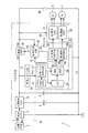
発電装置付き電子時計1は、図1に示すように、発電装置2と、二次電池3と、主電源補助コンデンサ4と、第1モータ6と、第2モータ7と、半導体装置(IC)10と、モータ駆動電圧補助コンデンサ60とを備えている。なお、本実施形態では、モータ駆動電圧補助コンデンサ60を半導体装置10の外部に設けているが、半導体装置10内に含ませて構成してもよい。
[First Embodiment]
DESCRIPTION OF EXEMPLARY EMBODIMENTS Hereinafter, a first embodiment of the invention will be described with reference to the drawings.
[Overall configuration of electronic watch with power generator]
As shown in FIG. 1, the electronic timepiece 1 with a power generator includes a power generator 2, a
発電装置2は、時計用に用いられる各種の発電装置が利用できる。例えば、回転錘等で運動エネルギを発生させ、そのエネルギを捉えてロータを回転させて発電する回転型の発電装置や、ソーラーパネルなどで光エネルギを捉えて発電するソーラー型の発電装置などが利用できる。 As the power generation device 2, various power generation devices used for watches can be used. For example, rotating power generators that generate kinetic energy with a rotating weight, etc., rotate the rotor by capturing the energy, and solar power generators that generate light by capturing light energy with solar panels, etc. it can.
二次電池3は、発電装置2で発電された電気エネルギを充電可能な蓄電手段(二次電源)であり、具体的には、リチウムイオン電池等の公知の二次電池で構成されている。
主電源補助コンデンサ4は、主電源である二次電池3を補助するために設けられている。例えば、二次電池3は容量も大きく内部抵抗もあるため、充電を開始してからIC10を駆動可能な電圧になるまで時間がかかる。一方、主電源補助コンデンサ4は、二次電池3に比べると容量が小さいが、充電開始時に迅速にIC10を駆動可能な電圧にすることができる。
従って、二次電池3および主電源補助コンデンサ4を設けることで、充電開始時には迅速に電圧を上昇させてIC10の起動性を確保でき、かつ、電源の容量も大きく確保してIC10を駆動する持続時間も長くできる。
The
The main power supply auxiliary capacitor 4 is provided to assist the
Therefore, by providing the
モータ6,7は、ステッピングモータなどで構成されている。モータ6,7で駆動される対象は、電子時計1の種類に応じて設定される。
例えば、第1モータ6で電子時計1の時針、分針を駆動し、第2モータ7で秒針を駆動してもよい。また、第1モータ6で時針、分針、秒針を駆動し、第2モータ7で日車やその他の情報を指示する指針を駆動してもよい。
The
For example, the hour and minute hands of the electronic timepiece 1 may be driven by the
[半導体装置]
半導体装置(半導体素子、IC)10は、整流回路11、充電制御回路12、定電圧発生回路13、定電圧駆動部20、電源回路30、電源制御回路40、駆動回路50を備えて構成されている。
また、定電圧駆動部20は、発振回路21、分周/クロック制御回路22、CPU(中央演算処理回路)23、制御ロジック回路24、第1駆動制御回路25、第2駆動制御回路26を備えている。
[Semiconductor device]
A semiconductor device (semiconductor element, IC) 10 includes a
The constant
整流回路11は、発電装置2から出力される交流電流を整流するものであり、全波整流回路、半波整流回路などの公知の整流回路が利用できる。
充電制御回路12は、整流回路11で整流された電流を、二次電池3および主電源補助コンデンサ4に充電する際の制御を行うものである。なお、充電制御回路12は、二次電池3の電圧が低い場合でも、二次電池3の電圧に所定の電圧を上乗せし、見かけ上電圧を高くしてIC10を駆動するクイックスタート回路や、二次電池3の電圧を昇降圧する昇降圧回路を含んで構成されている。
The
The charging
定電圧発生回路13は、主電源電圧VDDで動作され、電圧VDDよりも低い定電圧VREGを発生させ、定電圧駆動部20に供給する。従って、発振回路21、分周/クロック制御回路22、CPU(中央演算処理回路)23、制御ロジック回路24、第1駆動制御回路25、第2駆動制御回路26は、定電圧VREGで作動される。定電圧駆動部20の各回路を、主電源電圧VDDではなく、それよりも低い定電圧VREGで駆動するのは、各回路の消費電流を低減するためである。
The constant
発振回路21は、水晶振動子等を備えており、所定周波数の信号を出力する。分周/クロック制御回路22は、発振回路21からの信号を分周し、分周により得られた各種基準信号をCPU23、制御ロジック回路24に出力する。
CPU23および制御ロジック回路24は、供給されたクロックで動作する。制御ロジック回路24は、CPU23でのソフト命令を処理し、処理結果を電源制御回路40や各駆動制御回路25,26に出力する。
The
The
駆動制御回路25,26は、制御ロジック回路24の処理結果に基づいて、モータ駆動パルスや、正転/逆転/運針周期等の各駆動形態に応じた運針タイミングを作成し、駆動回路50の第1駆動回路51、第2駆動回路52にそれぞれモータ駆動パルスを出力する。
Based on the processing result of the
電源制御回路40は、CPU23からのソフト命令を制御ロジック回路24で処理したEnable信号81に応じて動作する。具体的には、電源制御回路40は、電源回路30の出力側であるモータ駆動電圧VDMを監視し、その監視結果に基づいて、電源回路30へオンオフ制御信号82を出力して電源回路30の動作を制御する。
The power
電源回路30は、電源制御回路40からのオンオフ制御信号82によりオンオフ制御され、オン制御の場合は主電源からの電気エネルギをモータ駆動電圧VDMとして出力する。そして、電源回路30は、オン制御時にはモータ駆動電圧補助コンデンサ60を電圧VDMレベルに充電する。モータ駆動電圧補助コンデンサ60は、モータ駆動時に流れる大電流によって、モータ駆動電圧が急峻に降下するのを防ぐために設けられている。
また、電源回路30がオフ制御されると、主電源からの電気エネルギの供給が遮断されるため、モータ駆動電圧補助コンデンサ60に充電された電気エネルギがモータ駆動電圧VDMとして出力され、駆動回路50が駆動される。
そして、電源回路30がオフ制御された状態で駆動回路50を駆動すると、モータ駆動電圧VDMが低下する。このため、電源制御回路40は、モータ駆動電圧VDMが所定電圧以下に低下すると電源回路30をオン制御し、再度、主電源からの電気エネルギをモータ駆動電圧VDMとして出力することで、モータ駆動電圧VDMを一定に維持できるように制御することができる。
The
When the
When the
駆動回路50の第1駆動回路51、第2駆動回路52は、電源回路30の出力であるモータ駆動電圧VDMで駆動する。そして、各駆動回路51,52は、駆動制御回路25,26から出力されるモータ駆動パルスに応じて、電圧VDMレベルのモータ制御信号をモータコイルに印加し、第1モータ6、第2モータ7を駆動電圧VDMで駆動する。
The
[電源制御回路の構成]
電源制御回路40は、図2に示すように、分圧手段41と、コンパレータ42を備えて構成され、制御ロジック回路24から出力されるEnable信号81がHighレベルになると動作状態となる。
コンパレータ42は、基準電圧を所定の仕事関数差で作成している。このため、コンパレータ42の(−)端子をVSS(0V)に接続すると、基準電圧=仕事関数差となる。本実施形態では、基準電圧=仕事関数差=1Vに設定してある。
[Configuration of power supply control circuit]
As shown in FIG. 2, the power
The
分圧手段41は、抵抗411,412,413,414と、スイッチとなる電界効果型トランジスタ415とを備えている。そして、電界効果型トランジスタ415がEnable信号81でオンされると、電源回路30の出力電圧VDMを所定の分圧比(前記各抵抗411〜414の抵抗値で設定)で分圧し、A点の分圧結果をコンパレータ42の(+)端子へ入力する。
分圧手段41の分圧比は、モータ駆動電圧を所定の定電圧、例えば1.35Vの定電圧にしたい場合は、VDM=1.35Vの時にA点がコンパレータの基準電圧である1Vになるように設定する。
この場合、前記オンオフ制御信号82となるコンパレータ42の出力は、電圧VDM<1.35V時に非検出状態(Lowレベル出力)、電圧VDM≧1.35V時に検出状態(Highレベル出力)となる。
The voltage dividing means 41 includes
The voltage dividing ratio of the voltage dividing means 41 is such that when the motor driving voltage is set to a predetermined constant voltage, for example, 1.35V, the point A becomes 1V which is the reference voltage of the comparator when VDM = 1.35V. Set to.
In this case, the output of the
[電源回路の構成]
電源回路30は、P型の電界効果型トランジスタ31を備えて構成されている。
そして、電源回路30から出力されるモータ駆動電圧VDMが1.35V未満の場合、コンパレータ42からのオンオフ制御信号82はLowレベルとなり、電界効果型トランジスタ31はオンされ、主電源電圧VDD=モータ駆動電圧VDMとなる。
電界効果型トランジスタ31がオンされると、モータ駆動電圧補助コンデンサ60は、電源回路30から出力される電気エネルギが充電され、モータ駆動電圧補助コンデンサ60の電圧もモータ駆動電圧VDMとなる。
[Configuration of power supply circuit]
The
When the motor drive voltage VDM output from the
When the
一方、電界効果型トランジスタ31がオンされて、前記モータ駆動電圧VDMが1.35V以上となった場合は、コンパレータ42からのオンオフ制御信号82はHighレベルとなり、電界効果型トランジスタ31はオフされ、モータ駆動電圧補助コンデンサ60の充電は遮断される。
そして、上記の電界効果型トランジスタ31のオン・オフ制御を、コンパレータ42の検出速度で繰り返すことで、電源回路30の出力はほぼ1.35Vの定電圧となる。
On the other hand, when the
By repeating the on / off control of the
電界効果型トランジスタ31は、オンオフ制御の応答速度を速くするため、ゲート端子の寄生容量を小さくする必要がある。すなわち、電界効果型トランジスタ31の応答速度が遅いと、図3に示すように、電源回路30の出力電圧VDMは三角波形のようになり定電圧とならない。例えば、出力電圧VDMがコンパレータ42の検出電圧(定電圧)以上になっても電界効果型トランジスタ31が即座にオフされないため、図3のA期間のように電圧がさらに上昇してしまう。また、電界効果型トランジスタ31がオフされ、負荷電流によって電圧が下降して出力電圧VDMがコンパレータ42の検出電圧未満になっても電界効果型トランジスタ31が即座にオンされないため、図3のC期間のように電圧がさらに下降してしまう。このため、電源回路30の出力電圧VDMは三角波形のようになってしまう。
The
このような現象を防ぐには、電界効果型トランジスタ31の応答速度を速くする必要があり、そのためには電界効果型トランジスタ31のサイズを小さくしてゲート端子の寄生容量を小さくする必要がある。
また、モータ駆動電圧VDMの損失を低減するためには、駆動能力を大きくする必要がある。このためには、電界効果型トランジスタ31のサイズを大きくする必要がある。
以上の要求性能を両立するため、電界効果型トランジスタ31は、サイズを小さくしてゲート端子の寄生容量を小さくするとともに、駆動能力が大きくなるように閾値電圧を低く設定してある。
In order to prevent such a phenomenon, it is necessary to increase the response speed of the
In order to reduce the loss of the motor drive voltage VDM, it is necessary to increase the drive capability. For this purpose, it is necessary to increase the size of the
In order to achieve both of the above required performances, the
一方で、電界効果型トランジスタ31の閾値電圧を低くすると、電界効果型トランジスタ31のOFFリーク電流が増加する。OFFリーク電流が増加し、OFFリーク電流が電源回路30の負荷電流よりも大きくなると、電界効果型トランジスタ31がオフとなっていても、OFFリーク電流によりモータ駆動電圧補助コンデンサ60は充電され、電源回路30の出力は定電圧とならない。
これを回避するため、電源回路30の負荷に分圧手段41を接続し、OFFリーク電流が電源回路30の負荷電流未満となるようにしている。
On the other hand, when the threshold voltage of the
In order to avoid this, the voltage dividing means 41 is connected to the load of the
また、電界効果型トランジスタ31は寄生ダイオード32を備えているが、この寄生ダイオード32は、アノードがモータ駆動電圧VDM側の電源ラインに接続され、カソードが主電源VDD側の電源ラインに接続されるように、サブストレートを主電源VDDへ接続している。
これは、電界効果型トランジスタ31がオフとなり、モータ駆動電圧補助コンデンサ60の充電が遮断状態の時、寄生ダイオード32の順方向電流によりモータ駆動電圧補助コンデンサ60が充電されることを防止するためである。
The
This is to prevent the motor driving
以上のように、応答速度の速い電界効果型トランジスタ31を用いることにより、図4に示すように、モータ駆動電圧VDMがコンパレータ42の検出電圧つまり定電圧からずれると即座にオンオフ制御信号82によって電界効果型トランジスタ31つまり電源回路30がオンオフ制御され、モータ駆動電圧VDMは、ほぼ定電圧に維持される。なお、前述の通り、電源回路30は、オンオフ制御信号82がHighレベルのときオフされ、Lowレベルのときオンされる。
As described above, by using the
[駆動回路の構成]
第1駆動回路51は、図2に示すように、4つの電界効果型トランジスタ511,512,513,514を備えている。
各トランジスタ511,512,513,514は、第1駆動制御回路25から出力されるモータ駆動パルスP11〜P14によって、それぞれ独立してオン・オフ制御を行うことができる。
そして、トランジスタ511,512は直列に接続され、トランジスタ513,514も直列に接続され、各トランジスタ511,512と、トランジスタ513,514とは並列に接続されている。
また、第1モータ6のコイルは、トランジスタ511および512間と、トランジスタ513および514間にそれぞれ接続されている。
[Configuration of drive circuit]
The
Each of the
The
The coil of the
第2駆動回路52は、図2に示すように、第1駆動回路51と同じ構成であり、4つの電界効果型トランジスタ521,522,523,524を備えている。
各トランジスタ521,522,523,524は、第2駆動制御回路26から出力されるモータ駆動パルスP21〜P24によって、それぞれ独立してオン・オフ制御を行うことができる。
なお、各トランジスタ521〜524の接続や、第2モータ7のコイルの接続は第1駆動回路51と同一なので説明を省略する。
As shown in FIG. 2, the
Each of the
In addition, since the connection of each transistor 521-524 and the connection of the coil of the 2nd motor 7 are the same as the
[モータ駆動制御処理]
次に、本実施形態におけるモータ駆動制御処理に関して説明する。
本実施形態では、モータ6,7を主電源電圧VDDで駆動する主電源駆動モードと、定電圧で駆動する定電圧駆動モードとを選択できるようにされている。なお、この選択は、制御対象のモータ6,7の種類や動作状態などに基づいて行われる。この際、利用者等による手動設定で選択してもよいし、CPU23による自動設定で選択してもよい。
[Motor drive control processing]
Next, the motor drive control process in this embodiment will be described.
In the present embodiment, a main power supply drive mode in which the
(主電源駆動モード:電源回路オン制御)
モータ6,7が主電源電圧VDD駆動の時は、制御ロジック回路24から電源制御回路40に出力されるEnable信号81はLowレベルとされる。このため、分圧手段41はオフとなり、コンパレータ42はDisableとなり、電源制御回路40から電源回路30に出力されるオンオフ制御信号82はLowレベルとなる。
このため、電界効果型トランジスタ31はオン状態となり、電源回路30はオン制御とされる。そして、モータ駆動電圧補助コンデンサ60は、二次電池3に接続され、主電源電圧VDDレベルまで充電される。この際、モータ駆動電圧VDMは主電源電圧VDDと一致し、例えば図5に示すように、VDD=1.58Vの場合、VDM=1.58Vとなる。
(Main power drive mode: Power circuit ON control)
When the
For this reason, the
(定電圧駆動モード)
定電圧駆動モードが選択された場合には、まず、主電源電圧VDDになっているモータ駆動電圧VDMを迅速に定電圧に低下させるための放電制御(電源回路オフ制御)を行い、モータ駆動電圧VDMが定電圧に低下した後は、モータ駆動電圧VDMを一定の定電圧に維持するための電源回路オンオフ制御を行う。
(Constant voltage drive mode)
When the constant voltage drive mode is selected, first, discharge control (power supply circuit off control) is performed to quickly reduce the motor drive voltage VDM, which is the main power supply voltage VDD, to the constant voltage. After the VDM drops to a constant voltage, power supply circuit on / off control is performed to maintain the motor drive voltage VDM at a constant constant voltage.
(放電制御:電源回路オフ制御)
定電圧駆動モードになると、CPU23は制御ロジック回路24に第1駆動回路51を利用した放電制御を指示する。制御ロジック回路24は、放電開始信号84を出力し、第1駆動制御回路25は、放電用のモータ駆動パルスを出力し、第1駆動回路51を放電回路として利用して放電電流を流す。
具体的には、CPU23は、ソフト命令により、制御ロジック回路24からEnable信号81を出力し、電源制御回路40を動作状態とする。
電源制御回路40は、コンパレータ42で、電圧VDMが、モータ6,7を定電圧駆動する際の定電圧(本実施形態では1.35V)以上であるかを検出する。例えば、前述のように、電圧VDD=1.58Vであれば、コンパレータ42は、電圧VDMが1.35V以上であることを検出し、Highレベルのオンオフ制御信号82を出力し、電源回路30をオフ制御する。
これにより、電界効果型トランジスタ31がオフされ、主電源からモータ駆動電圧補助コンデンサ60への充電が遮断される。
(Discharge control: Power circuit off control)
In the constant voltage drive mode, the
Specifically, the
The power
Thereby, the
次に、CPU23は、制御ロジック回路24から放電開始信号84を出力させ、第1駆動制御回路25から第1駆動回路51を放電回路とするためのモータ駆動パルスP11〜P14を出力させる。
すなわち、第1駆動制御回路25は、CPU23のソフト命令に応じて処理を行う制御ロジック回路24からの指示により、P11=Lowレベル、P12=Highレベル、P13=Highレベル、P14=Lowレベルのモータ駆動パルスを出力する。
Next, the
That is, the first drive control circuit 25 is a motor of P11 = Low level, P12 = High level, P13 = High level, and P14 = Low level according to an instruction from the
上記のモータ駆動パルスP11〜P14に応じて、第1駆動回路51を構成する4つの電界効果型トランジスタ511,512,513,514は、トランジスタ511:オン、512:オン、513:オフ、514:オフとなる。このため、図6に示すように、モータ駆動電圧補助コンデンサ60から電界効果型トランジスタ511,512を経由して放電電流が流れ、図5に示すように、モータ駆動電圧補助コンデンサ60を定電圧(1.35V)まで放電させる。
なお、放電電流は数mAであり、放電時間はusecオーダーであり、例えば1秒間隔で行われる秒針のステップ運針の間でも十分に処理できる。このため、放電期間中は、各モータ6,7の駆動は禁止されている。
In response to the motor driving pulses P11 to P14, the four
The discharge current is several mA, the discharge time is in the usec order, and can be sufficiently processed even during the second hand stepping performed at intervals of 1 second, for example. For this reason, driving of the
モータ駆動電圧補助コンデンサ60の放電中、電源制御回路40はコンパレータ42で電圧VDMが定電圧(1.35V)未満まで低下したかを検出する。そして、電圧VDMが定電圧未満になると、電源制御回路40は、図1に示すように、放電終了信号83を制御ロジック回路24に出力し、制御ロジック回路24は第1駆動制御回路25を介して第1駆動回路51の放電制御を停止させる。
なお、モータ駆動電圧補助コンデンサ60は、容量、種類によっては放電終了後に電圧が復帰する時もあるが、この時は、上記放電制御を数回繰り返す事で、確実に定電圧まで放電すればよい。
During the discharge of the motor drive voltage
The motor drive voltage
(電源回路オンオフ制御)
モータ駆動電圧補助コンデンサ60が放電制御によって定電圧までに低下した後は、電源制御回路40から出力されるオンオフ制御信号82により電界効果型トランジスタ31をオンオフ制御することで、モータ駆動電圧VDMが定電圧に維持される。
すなわち、図4に示すように、モータ駆動電圧VDMが定電圧以上になれば電界効果型トランジスタ31をオフし、定電圧未満になればオンすることを繰り返すことで、電圧VDMをほぼ定電圧に維持できる。このため、各モータ6,7を定電圧で確実にかつ安定して駆動できる。
(Power circuit on / off control)
After the motor drive voltage
That is, as shown in FIG. 4, the
なお、前記実施形態では、第1駆動回路51を放電回路として利用する場合について説明したが、第2駆動回路52を放電回路として利用してもよい。この場合は、制御ロジック回路24から第2駆動回路52を放電回路とする放電開始信号85を第2駆動制御回路26に出力し、第2駆動制御回路26から放電用のモータ駆動パルスP21〜24を出力して第2駆動回路52を放電回路とする制御、つまり前記第1駆動制御回路25および第1駆動回路51と同じ制御を行えばよい。
In the above embodiment, the case where the
このような本実施形態によれば、次のような効果がある。
(1)電源回路30および電源制御回路40を設けたので、モータ駆動電圧VDMを主電源電圧VDDと一致させる主電源駆動モードと、モータ駆動電圧VDMを定電圧に維持する定電圧駆動モードとを選択して制御することができる。
すなわち、電源制御回路40を停止させると、オンオフ制御信号82がLowレベルになって電源回路30の電界効果型トランジスタ31をオンし続けるため、モータ駆動電圧VDMが主電源電圧VDDと一致する主電源駆動モードで制御できる。
一方、電源制御回路40を作動させると、モータ駆動電圧VDMをコンパレータ42で定電圧と比較し、その比較結果に応じて電界効果型トランジスタ31をオン・オフ制御するため、モータ駆動電圧VDMを定電圧に維持できる。
従って、電源制御回路40を作動させるだけで、モータ駆動電圧VDMを定電圧に容易に維持でき、モータ6,7を作動電圧範囲内の一定の電圧で駆動でき、モータ6,7を確実にかつ安定して駆動することができる。
According to this embodiment, there are the following effects.
(1) Since the
That is, when the power
On the other hand, when the power
Therefore, the motor drive voltage VDM can be easily maintained at a constant voltage by only operating the power
(2)さらに、電源制御回路40は、実際のモータ駆動電圧VDMを定電圧と比較して電源回路30をオン・オフ制御しているので、従来のように、主電源電圧VDDを、2/3や1/3等に降圧する降圧回路を用いた場合のように、主電源電圧VDDの変動に影響されることがなく、二次電池3の充電などによって主電源電圧VDDが変化しても、モータ駆動電圧VDMを確実に定電圧に維持することができる。
また、主電源電圧に影響されずに、モータ6,7を定電圧駆動制御できるため、モータ6,7が駆動中であっても、発電装置2から二次電池3への充電を継続することができ、充電効率も向上することができる。
(2) Further, the power
In addition, since the
(3)モータ駆動電圧補助コンデンサ60の電気エネルギを放電させる放電手段を備えているので、モータ駆動電圧VDMを迅速に定電圧に低下させることができ、モータ駆動に遅延が生じることも防止できる。
すなわち、降圧回路の時定数によってモータ駆動電圧VDMが定電圧に低下するまでに時間がかかる従来技術では、時定数に応じた待機時間を設定し、モータ駆動に遅延が生じる。
これに対し、本実施形態では、放電手段を設けてモータ駆動電圧補助コンデンサ60の電気エネルギを放電しているので、モータ駆動電圧VDMを迅速に定電圧に低下させることができ、モータ駆動に遅延が生じることも防止できる。
(3) Since the discharge means for discharging the electric energy of the motor drive voltage
That is, in the conventional technique that takes time until the motor drive voltage VDM drops to a constant voltage due to the time constant of the step-down circuit, a standby time corresponding to the time constant is set, and the motor drive is delayed.
On the other hand, in the present embodiment, the discharge means is provided to discharge the electric energy of the motor drive voltage
(4)モータ駆動電圧補助コンデンサ60を設けているので、モータ駆動時に大電流が流れても、モータ駆動電圧が急激に低下することを防止でき、モータ駆動電圧を所定の定電圧に維持でき、モータを確実にかつ安定して駆動することができる。
(4) Since the motor driving
(5)放電手段として、モータ駆動パルスP11〜P14で各電界効果型トランジスタ511〜514の作動を制御することで、第1駆動回路51を利用して放電しているので、抵抗素子、定電流素子などの専用の放電素子で放電する場合に比べて、モータ駆動制御回路の構成を簡易にでき、その回路サイズも小さくでき、IC10を小型化できる。
(5) As the discharge means, by controlling the operation of each of the
(6)電源回路30は、電界効果型トランジスタ31を用いて構成しているので、小さなゲート電流でオン・オフ制御でき、IC10に容易に組み込むことができる。
さらに、電界効果型トランジスタ31がオフされている際に、主電源からモータ駆動電圧補助コンデンサ60に充電が行われることを防止する寄生ダイオード32を備えているので、電界効果型トランジスタ31をオフしてモータ駆動電圧VDMを低下させたい際に、充電によってモータ駆動電圧VDMが上昇するようなことも防止でき、定電圧制御を安定して行うことができる。
(6) Since the
Further, since the
(7)電源制御回路40を、分圧手段41およびコンパレータ42を備えて構成しているので、コンパレータ42の検出電圧の温度特性、IC製造時の量産バラツキを小さくできる。すなわち、コンパレータ42を構成するトランジスタの閾値電圧は、同方向に変化するようにしてあり、かつ、コンパレータ42の基準電圧である仕事関数差=閾値電圧差は変化しない。また、分圧手段41のA点から得られる分圧結果も、分圧手段41を構成する各抵抗は同方向に変化するため、分圧比が変化せず、分圧結果は変化しない。従って、コンパレータ42は検出誤差が小さくなり、精度の高い制御を行うことができる。
(7) Since the power
(8)分圧手段41を電源回路30の負荷としているので、電源回路30の電界効果型トランジスタ31の閾値電圧を低くでき、且つ、サイズ(面積)も小さくすることができる。
また、電界効果型トランジスタ31がオフとなっている時、OFFリーク電流による主電源からモータ駆動電圧補助コンデンサ60に充電が行われることを防止でき、モータ駆動電圧の定電圧制御を安定して行うことができる。
(8) Since the voltage dividing means 41 is used as the load of the
In addition, when the
(9)さらに、主電源駆動モードと定電圧駆動モードを選択できるように構成したので、モータ6,7として作動領域の異なるモータを用いた場合に、各モータ6,7に適した電圧を加えることができ、各モータ6,7を効率的に駆動することができる。例えば、第1モータ6として作動領域が比較的広いモータを用い、第2モータ7として作業領域が狭いモータを用い、第1モータ6を駆動する際には主電源駆動モードを選択すれば、高負荷の駆動も可能となり、重厚な時刻表示用指針220を設けて効率的に駆動することもできる。また、第2モータ7を駆動する際には定電圧駆動モードを選択すれば、作動領域が狭いモータ7を効率的に駆動することができる。
(9) Further, since the main power supply drive mode and the constant voltage drive mode can be selected, when a motor having a different operation area is used as the
[第2実施形態]
次に、本発明の第2実施形態について、図7を参照して説明する。
本実施形態では、前記第1実施形態の電源制御回路40における分圧手段41を改良し、モータ駆動電圧補助コンデンサ60のモータ駆動電圧VDMを複数段階に切替可能に構成したものである。なお、その他の構成は、前記第1実施形態と同一であるため、説明を省略する。
[Second Embodiment]
Next, a second embodiment of the present invention will be described with reference to FIG.
In this embodiment, the voltage dividing means 41 in the power
本実施形態の分圧手段41Aは、前記分圧手段41と同様に、4つの抵抗411〜414と、電界効果型トランジスタ415とを備えると共に、各抵抗411〜413と、モータ駆動電圧VDMの電源ラインとの間に、スイッチとなる電界効果型トランジスタ416〜418が設けられている。各トランジスタ416〜418は、CPU23のソフト命令による制御ロジック回路24からの切替え信号SA〜SCによって、オン・オフが制御され、これにより分圧手段41Aの分圧比を切替え可能に構成されている。
Similar to the voltage dividing means 41, the voltage dividing means 41A of this embodiment includes four
本実施形態では、切替え信号SBによってトランジスタ417をオンすると、A点では、直列接続された抵抗412,413の抵抗値と、抵抗414の抵抗値の比率に基づいてモータ駆動電圧VDMを分圧した電圧が生じ、この電圧がコンパレータ42で基準電圧と比較される。
一方、切替え信号SAによってトランジスタ416をオンすると、各抵抗411,412,413が直列に接続されるため、電圧VDMの電圧降下がより大きくなる。従って、切替え信号SBでトランジスタ417をオンした場合の検出電圧に比べて、切替え信号SAでトランジスタ416をオンした場合のほうが、検出電圧は高くなる。
逆に、切替え信号SCによってトランジスタ418をオンすると、抵抗413のみで電圧降下が生じるため、切替え信号SBでトランジスタ417をオンした場合の検出電圧に比べて、切替え信号SCでトランジスタ418をオンした場合のほうが、検出電圧は低くなる。
これにより、モータ駆動電圧である定電圧を3段階に切替え可能となる。
なお、第2実施形態では、定電圧を3段階に切替えているが、抵抗やスイッチとなるトランジスタの数を適宜設定することなどで、2段階、或いは、4段階以上の定電圧切替えを可能な構成にしてもよい。
In this embodiment, when the
On the other hand, when the
On the contrary, when the
Thereby, the constant voltage which is a motor drive voltage can be switched in three stages.
In the second embodiment, the constant voltage is switched in three stages. However, the constant voltage can be switched in two stages or in four stages or more by appropriately setting the number of transistors serving as resistors and switches. It may be configured.
このような第2実施形態によれば、前記第1実施形態と同じ作用効果を奏することができる上、次のような効果もある。
(2−1)モータ駆動電圧である定電圧を3段階に切り替えることができるため、モータ駆動電圧を、モータ6,7の使用条件などに応じて最適な定電圧に設定することができ、モータ6,7を効率よく駆動することができる。
According to such 2nd Embodiment, there can exist the same effect as the said 1st Embodiment besides the following effects.
(2-1) Since the constant voltage that is the motor drive voltage can be switched in three stages, the motor drive voltage can be set to an optimum constant voltage according to the use conditions of the
[第3実施形態]
次に、本発明の第3実施形態について説明する。
第3実施形態の発電装置付き電子時計1Bは、手巻き発電機構と、発電状態表示機構とを備えている点が前記実施形態と大きく相違する。但し、モータ6,7の駆動を制御する半導体装置10の構成に関しては前記第1実施形態と同様であるため、説明を省略あるいは簡略する。
[Third Embodiment]
Next, a third embodiment of the present invention will be described.
The
電子時計1Bは、図8に示すように、時針221、分針222、秒針223からなる時刻表示用指針220を備えており、この時刻表示用指針220は前記第1モータ6によって駆動される。
また、電子時計1Bの文字板224の9時位置には、時刻表示用指針220とは別に設けられる発電表示用指針である表示針(副表示針)231および発電表示用目盛板232が設けられている。発電表示用目盛板232には、所定の目盛321が表示され、表示針231を第2モータ7で駆動して、目盛321を指示することで発電状態を表示可能とされている。
なお、文字板224の3時位置には窓241が形成され、文字板224の裏面に配置された日車によって日付が表示可能とされている。この日車は、図示略の日車用モータで回転駆動される。
As shown in FIG. 8, the electronic timepiece 1 </ b> B includes a
In addition, at the 9 o'clock position of the
A
電子時計1Bは、発電装置2として、回転錘の回転エネルギでロータを回転することで発電する発電装置を内蔵している。
この発電装置のロータは、りゅうず203を回すことでも発電可能とされている。この回転錘による自動巻発電と、りゅうず203による手巻き発電とを実現する具体的な構成は、本出願人が既に出願した特願2006-276156号や、特願2006-276157号の明細書に開示されたものと同じであるため、説明を省略する。
The
The rotor of this power generation device can also generate power by turning the
そして、前記第2モータ7で駆動される表示針231は、通常は、二次電池3に充電された電気エネルギ量に応じて電子時計1Bの動作持続時間を表示するとともに、りゅうず203を操作した手巻き機構により発電した場合は、その発電量を表示するように制御されている。
ここで、第2モータ7は、特に、手巻きによる発電量を表示する際は、高速で正転及び逆転駆動をさせる必要があり、1秒に1回正転駆動する第1モータ6と比較し、充電による主電源VDDの変動幅に対応してモータ7の作動電圧範囲を広く確保することが非常に困難である。
従って、この時計1Bでは、第1モータ6のみ駆動させる際は、モータ駆動電圧を主電源VDDと同電圧とし、第1モータ6および第2モータ7を駆動させる際は、第2駆動回路52により放電制御を行った後、第1モータ6および第2モータ7の各モータ駆動電圧を定電圧としている。
The
Here, especially when displaying the amount of power generated by manual winding, the second motor 7 needs to be rotated forward and reverse at a high speed, and compared with the
Therefore, in the
本実施形態のモータ駆動制御処理に関し、図9,10のフローチャートおよび図11のタイミングチャートを用いて説明する。
まず、初期状態では、電源制御回路40は作動されておらず、このため、電源回路30はオン状態とされており、モータ駆動電圧VDMは主電源電圧VDDと一致している(ステップS1)。
The motor drive control process of the present embodiment will be described using the flowcharts of FIGS. 9 and 10 and the timing chart of FIG.
First, in the initial state, the power
続いて、CPU23は、第1駆動制御回路25および第1駆動回路51を介して第1モータ6を毎秒運針駆動で制御し、時刻表示用指針220で時刻を表示する。また、CPU23は、第2駆動制御回路26および第2駆動回路52を介して第2モータ7を駆動し、表示針231で現在の動作持続時間を指示する(ステップS2)。
Subsequently, the
なお、持続時間は、例えば、二次電池3の電圧を検出し、その電圧値に基づいて算出してもよいし、発電装置2の発電電流つまり二次電池3への充電電流を積算して求めてもよい。
また、持続時間は、例えば、目盛321の1目盛が1日などに設定されるため、一旦、持続時間の指示を行うと、持続時間が変更されるまではその指示を継続すればよい。すなわち、持続時間の目盛が1日単位の場合には、発電が無くて1日経過したために持続時間も1日減少した場合や、発電が行われて1日分の持続時間が増加した場合に第2モータ7を駆動して、表示針231を1日分、増加あるいは減少すればよい。従って、持続時間表示の変更が必要ない間は、第2モータ7の駆動つまり表示針231の運針は停止されている。
このような持続時間の算出および表示の方法は、本出願人が出願した特願2007-065646号の明細書に記載された方法などを用いればよい。
The duration may be calculated, for example, by detecting the voltage of the
Further, for example, since one scale of the
As a method for calculating and displaying such a duration, the method described in the specification of Japanese Patent Application No. 2007-065646 filed by the present applicant may be used.
続いて、CPU23は、手巻き発電が行われているか否かを判定する(ステップS3)。ここで、手巻き発電が行われていた場合には、CPU23は、発電量表示処理を実行する(ステップS4)。
なお、手巻き発電の判定は、例えば、りゅうず203の回転を検出したり、手巻き発電時の発電電流の変化の特徴などに基づいて判定すればよい。
Subsequently, the
Note that manual winding power generation may be determined based on, for example, detection of rotation of the
発電量表示処理が実行されると、図10に示すように、CPU23は制御ロジック回路24を介して電源制御回路40を作動する(ステップS11)。
そして、CPU23は、制御ロジック回路24から第2駆動制御回路26に対し放電開始信号85を出力させ、第2駆動回路52による放電制御に移行する(ステップS12)。
When the power generation amount display process is executed, as shown in FIG. 10, the
Then, the
第2駆動制御回路26は、第2駆動回路52に対して、第2駆動回路52を放電回路とするためのモータ駆動パルスP21〜24を出力し、モータ駆動電圧補助コンデンサ60に充電されていた電荷を放電させる(ステップS13)。具体的には、図11に示すように、モータ駆動パルスP22、P23をHighレベルとし、モータ駆動パルスP21,P24はLowレベルのままに制御する。これにより、モータ駆動電圧補助コンデンサ60に充電されていた電気エネルギが第2駆動回路52を通って放電される。
そして、電源制御回路40のコンパレータ42で、モータ駆動電圧VDMが定電圧以下になったかを判定する(ステップS14)。ステップS14でNoと判定された場合には、ステップS13に戻りモータ駆動電圧補助コンデンサ60の放電を継続する。すなわち、モータ駆動電圧補助コンデンサ60の放電処理(S13)は、VDM≦定電圧となるまで継続する。
また、この放電の間、第1モータ6および第2モータ7はそれぞれ駆動が禁止されている。
The second
Then, the
Further, during the discharge, the
そして、電源制御回路40において、VDM≦定電圧となったことが判定されると(ステップS14)、電源制御回路40は放電終了信号83を制御ロジック回路24に出力し、制御ロジック回路24は第2駆動制御回路26を介して第2駆動回路52の放電制御を停止し、モータ駆動電圧補助コンデンサ60の放電処理を終了する(ステップS15)。
When the power
次に、CPU23は、電源制御回路40を利用してモータ駆動電圧VDMが定電圧となるように制御する(ステップS16)。すなわち、図11に示すように、モータ駆動電圧VDMがコンパレータ42の検出電圧(定電圧)よりも低下すると、コンパレータ42の出力信号であるオンオフ制御信号82がLowレベルとなり、電界効果型トランジスタ31がオンされて、主電源電圧VDDでモータ駆動電圧補助コンデンサ60が充電され、モータ駆動電圧VDMも上昇する。
一方、モータ駆動電圧VDMが上昇し、定電圧以上になると、オンオフ制御信号82がHighレベルとなり、電界効果型トランジスタ31がオフされて、モータ駆動に伴い、電圧VDMは下降する。
従って、モータ駆動電圧VDMの変化に応じて電界効果型トランジスタ31をオン・オフ制御することで、図11に示すように、モータ駆動電圧VDMは、コンパレータ42の検出電圧つまり定電圧でほぼ一定に維持される。
Next, the
On the other hand, when the motor drive voltage VDM increases and becomes equal to or higher than a constant voltage, the on / off
Therefore, by turning on / off the
そして、CPU23は、第1モータ6による毎秒運針制御および第2モータ7による発電量表示駆動制御を行う(ステップS17)。
すなわち、CPU23は、第1駆動制御回路25から出力されるモータ駆動パルスP11〜P14を制御して、第1モータ6を1秒ごとに正転し、時刻表示用指針220をステップ運針する。
Then, the
That is, the
また、CPU23は、第2駆動制御回路26から出力されるモータ駆動パルスP21〜P24を制御して、第2モータ7を正転あるいは逆転の早送り運針を行い、発電量を表示する。
例えば、図11の1段目に示すように、整流回路出力を所定のサンプリングレートでサンプリングし、その各サンプリング時の平均発電電流値を求め、その発電電流値の大きさに応じて表示針231を移動すればよい。なお、この発電量表示の制御方法は、本出願人が出願した特願2007-065646号の明細書に記載された方法などを用いればよい。
In addition, the
For example, as shown in the first stage of FIG. 11, the output of the rectifier circuit is sampled at a predetermined sampling rate, an average generated current value at each sampling is obtained, and the
次に、CPU23は、手巻き発電が継続しているかを確認する(ステップS18)。そして、手巻き発電が継続している場合には、前記ステップS16,S17の処理を繰り返す。
一方、手巻き発電が終了している場合には、図11に示すように、CPU23は、Enable信号81をLowレベルとし、電源制御回路40を停止する(ステップS19)。
そして、この電源制御回路40がDisableとされることで、電界効果型トランジスタ31はオンされ、電圧VDMは主電源電圧VDDと同じ電圧になる(ステップS20)。
以上により、発電量表示処理S4が終了する。
Next, the
On the other hand, when the manual winding power generation is completed, as shown in FIG. 11, the
When the power
Thus, the power generation amount display process S4 ends.
図9に示すように、発電量表示処理S4が終了した場合、あるいは、ステップS3で手巻き発電無しと判定された場合には、CPU23は運針制御停止か否かを判定する(ステップS5)。運針制御停止とは、例えば、長期間発電が行われなくなり、二次電池3の電圧がIC10を駆動可能な電圧以下に低下した場合など、運針制御を続行できなくなった状態を意味する。
従って、ステップS5で制御停止状態と判定されると制御を終了する。一方、制御停止ではないと判定されると、ステップS2に戻り、第1モータ6による運針制御および第2モータ7による持続時間表示が行われる。
As shown in FIG. 9, when the power generation amount display process S4 is completed or when it is determined in step S3 that there is no manual winding power generation, the
Accordingly, when it is determined in step S5 that the control is stopped, the control is terminated. On the other hand, if it is determined that the control is not stopped, the process returns to step S2, and the hand movement control by the
このような本実施形態によれば、前記各実施形態と同様の作用効果を得られるほか、次のような効果もある。
(3−1)手巻き発電時は、図11の1段目に示すように、発電電流値は大きく変化する。このため、発電状態を表示する表示針231を駆動する第2モータ7は、図11のモータ駆動パルスP21〜P24に示すように、正転方向や逆転方向に早送り駆動を行う必要があるが、本実施形態では、第2モータ7が駆動される場合には、モータ駆動電圧VDMを定電圧に制御しているため、第2モータ7を確実にかつ安定して早送り駆動できる。
According to the present embodiment as described above, the same operational effects as those of the respective embodiments can be obtained, and the following effects can also be obtained.
(3-1) At the time of manual winding power generation, as shown in the first stage of FIG. For this reason, the second motor 7 that drives the
(3−2)さらに、定電圧制御を行うのは、手巻き発電が行われている間だけであり、それ以外は、主電源駆動モードで駆動している。このため、制御用にエネルギが消費され、かつ、放電も行われる定電圧制御を常時継続する場合に比べて、省電力化を図ることができる。
また、手巻き発電時以外では、主電源電圧の変動も小さいため、主電源電圧VDDでモータ6,7を駆動しても確実にかつ安定して駆動することができる。なお、持続時間の指示を変更する場合は、発電状態の表示に比べて早送りで正転や逆転を行う必要がないために、第2モータ7を主電源電圧で駆動しても十分に安定して駆動できる。
(3-2) Furthermore, the constant voltage control is performed only during manual winding power generation, and the rest is driven in the main power supply driving mode. For this reason, power saving can be achieved compared with the case where constant voltage control in which energy is consumed for control and discharge is also continuously performed.
In addition, since the fluctuation of the main power supply voltage is small except during the manual power generation, even if the
(3−3)電子時計1は、発電状態(発電電流)に応じて移動する表示針231を備えているので、使用者は、発電装置2における発電状態をリアルタイムに確認することができる。このため、手巻き発電操作時に、発電量が十分であるかを確認でき、使用者は発電状態を確認しながら操作することで、手巻き発電操作を確実に行うことができる。 (3-3) Since the electronic timepiece 1 includes the display hands 231 that move according to the power generation state (power generation current), the user can check the power generation state in the power generation device 2 in real time. For this reason, it is possible to confirm whether the amount of power generation is sufficient during the manual winding power generation operation, and the user can reliably perform the manual winding power generation operation by performing the operation while confirming the power generation state.
(3−4)時刻表示用指針220とは別の表示針231で発電状態を表示しているので、時刻表示と発電状態の表示とを同時に行うことができる。このため、時刻表示用指針220を発電表示にも兼用する場合に比べて、利便性を向上できる。
さらに、発電状態を表示針231で表示できるので、タコメータのように、発電状態をリアルタイムにかつ視覚的に表示でき、使用者は発電状態を感覚的にかつ容易に把握できる。
(3-4) Since the power generation state is displayed by the
Furthermore, since the power generation state can be displayed with the
(3−5)表示針231は、通常時は持続時間を表示し、発電時に発電状態を表示しているので、互いに関連性の強い情報を同一の表示針231で表示でき、時計1Bの使用者も情報を容易に把握できる。その上、表示針231を兼用できるので、指針やモータを増やす必要が無く、電子時計1Bの構成を簡易化できる。
さらに、通常時には持続時間が表示されているので、使用者は、時計1Bが発電せずにどれくらい作動し続けるのかを把握でき、時計が停止する前に発電操作を行うことで、時計1Bが停止してしまうことも防止できる。
(3-5) Since the
Furthermore, since the duration time is normally displayed, the user can grasp how long the
なお、本発明は前述の実施形態に限定されるものではなく、本発明の目的を達成できる範囲での変形、改良等は本発明に含まれるものである。
例えば、放電手段としては、前記実施形態のように、モータの駆動回路51,52を利用したものに限らず、駆動回路51,52に設けられる回転検出用の抵抗を使用して放電してもよい。例えば、図12に示すように、駆動回路51に設けられる回転検出用の抵抗53を利用して放電する場合には、抵抗53に接続された電界効果型トランジスタ54をオンするとともに、電界効果型トランジスタ512をオンし、他のトランジスタ511,513,514をオフし、モータ駆動電圧補助コンデンサ60に充電された電気エネルギを、前記トランジスタ54、抵抗53、電界効果型トランジスタ512を介して放電すればよい。
It should be noted that the present invention is not limited to the above-described embodiments, and modifications, improvements, and the like within the scope that can achieve the object of the present invention are included in the present invention.
For example, the discharge means is not limited to the one using the
また、放電手段としては、モータコイルの抵抗を利用して放電してもよい。例えば、図13に示すように、第1モータ6を利用して放電する場合には、電界効果型トランジスタ511,514をオンし、電界効果型トランジスタ512,513をオフすると、モータ駆動電圧補助コンデンサ60に充電された電気エネルギは、前記トランジスタ511、モータコイル抵抗、トランジスタ514を介して流れて放電される。なお、放電制御は、前述のとおり、非常に時間が短く、モータ6を駆動するほどのエネルギを備えていないため、モータコイル抵抗を利用して放電した場合に、モータ6が駆動することはない。
また、モータ6の回転方向の極性と逆方向の極性で放電すれば、モータ6が放電制御により駆動することをより確実に防止できる。例えば、電界効果型トランジスタ512、513をオンした際にモータ6が回転する極性に設定されているのであれば、放電制御は電界効果型トランジスタ511、514をオンすれば、放電制御によりモータ6が駆動することはなく、確実に放電のみを行うことができる。
Moreover, as a discharge means, you may discharge using the resistance of a motor coil. For example, as shown in FIG. 13, when discharging using the
Further, if discharging is performed with the polarity opposite to the rotation direction of the
さらに、放電手段としては、駆動回路51,52を利用せずに、抵抗素子、定電流素子などの専用の放電素子を設けて放電するものでもよい。専用の放電素子を用いれば、放電量の調整を容易に行うことができる利点がある。
Further, as the discharging means, a discharge element may be provided by providing a dedicated discharge element such as a resistance element or a constant current element without using the
また、前記実施形態では、各モータ6,7の駆動電圧を同じ定電圧に調整していたが、各モータ6,7の定電圧をそれぞれ別々に設定してもよい。すなわち、複数のモータが設けられている場合、モータの用途や特性によっては、モータ毎に定電圧を異ならせる必要がある。この場合には、モータの駆動回路51,52毎に、電源回路30、電源制御回路40、モータ駆動電圧補助コンデンサ60を設け、モータ毎に定電圧を制御可能に構成すればよい。
Moreover, in the said embodiment, although the drive voltage of each
前記実施形態では、主電源駆動モードと定電圧駆動モードとを切り替えて制御可能にしていたが、制御対象のモータ6,7の種類や駆動速度などによっては、常時、定電圧駆動モードで駆動するようにしてもよい。
In the above embodiment, the main power supply drive mode and the constant voltage drive mode can be switched and controlled. However, depending on the type of the
前記実施形態では、2つのモータ6,7を設けていたが、本発明は、モータが1つの場合、あるいは3つ以上の場合でも適用することができる。
In the above embodiment, the two
発電装置2としては、前記実施形態のような手巻き発電装置および自動巻き発電装置を備えるものに限らず、回転錘のみで発電する手巻き発電機構を備えない自動巻き発電装置、光エネルギにより発電するソーラー発電装置、熱エネルギにより発電する熱発電装置、圧電効果を利用した圧電型発電装置、浮遊電波等の外部の誘導により発電する発電装置等の各種の発電装置が利用できる。また、電子時計1,1Bには、前記各種の発電装置を1種類組み込んでもよいし、前記実施形態のように、複数種類の発電装置を組み合わせてもよい。
また、本発明は、発電装置を備えるものに限らず、例えば、外部発電装置で発生する電気エネルギを内部の蓄電装置に蓄え、その電力で駆動する蓄電装置付き電子時計にも利用できる。つまり電子時計自体には発電装置を備えておらず、外部から充電される二次電池3等の蓄電装置を備えた電子時計にも本発明は適用できる。
The power generation device 2 is not limited to the one provided with the manual winding power generation device and the automatic winding power generation device as in the above-described embodiment, but the automatic winding power generation device that does not include the manual winding power generation mechanism that generates power only with the rotary weight, and generates power with light energy. Various power generators such as a solar power generator that generates power, a thermal power generator that generates power using thermal energy, a piezoelectric power generator that uses the piezoelectric effect, and a power generator that generates power by external induction such as floating radio waves can be used. The
In addition, the present invention is not limited to the one provided with the power generation device, and can be used, for example, in an electronic timepiece with a power storage device that stores electrical energy generated by the external power generation device in an internal power storage device and is driven by the power. That is, the electronic timepiece itself does not include a power generation device, and the present invention can also be applied to an electronic timepiece including a power storage device such as a
また、本発明の電子時計1は、液晶ディスプレイ、有機ELディスプレイ、電子泳動ディスプレイ等の各種の表示パネルを有する時計でもよい。
さらに、本発明は、腕時計に限らず、モータを備えていれば、懐中時計、置時計、掛け時計などの他の時計にも適用できるし、時計以外の各種の電子機器にも適用できる。
さらに、本発明は、半導体装置(半導体素子、IC)10をパッケージ化して外販し、各電子機器の製造メーカにおいて、本発明の半導体装置10を組み込んで使用してもよい。
要するに、本発明は、発電装置や外部から充電される二次電池3等を備えて電源電圧が変動する主電源を有し、かつ、モータを定電圧で駆動する必要がある場合に広く利用できる。
The electronic timepiece 1 of the present invention may be a timepiece having various display panels such as a liquid crystal display, an organic EL display, and an electrophoretic display.
Furthermore, the present invention is not limited to a wristwatch, and can be applied to other watches such as a pocket watch, a table clock, and a wall clock as long as a motor is provided, and can also be applied to various electronic devices other than a watch.
Furthermore, in the present invention, the semiconductor device (semiconductor element, IC) 10 may be packaged and sold externally, and each electronic device manufacturer may incorporate and use the
In short, the present invention can be widely used in the case where the power supply voltage varies with a power generation device or a
1,1B…発電機能付き電子時計、2…発電装置、3…二次電池、4…主電源補助コンデンサ、6…第1モータ、7…第2モータ、10…半導体装置(IC)、11…整流回路、12…充電制御回路、20…定電圧駆動部、23…CPU、24…制御ロジック回路、25…第1駆動制御回路、26…第2駆動制御回路、30…電源回路、31…電界効果型トランジスタ、32…寄生ダイオード、40…電源制御回路、41,41A…分圧手段、42…コンパレータ、51…第1駆動回路、52…第2駆動回路、53…抵抗、54…電界効果型トランジスタ、60…モータ駆動電圧補助コンデンサ、203…りゅうず、220…時刻表示用指針、231…表示針。
DESCRIPTION OF
Claims (16)
前記モータを駆動する駆動回路と、
前記主電源および駆動回路間に設けられて、主電源から供給される電気エネルギを用いて駆動回路へ駆動電圧を供給する電源回路と、
前記電源回路から供給される電気エネルギを蓄積する蓄電手段と、
前記電源回路の作動を制御する電源制御回路とを備え、
前記電源制御回路は、前記駆動回路を、主電源の電圧で駆動する主電源駆動モードと、前記所定の定電圧で駆動する定電圧駆動モードとを選択可能に構成され、
主電源駆動モードが選択された場合には、前記電源回路を作動して主電源から駆動回路へ電気エネルギを供給して駆動し、
定電圧駆動モードが選択された場合には、
前記駆動電圧を監視し、
前記駆動電圧が所定の定電圧以上の場合は、前記電源回路を停止して主電源から駆動回路への電気エネルギの供給を停止し、かつ、前記蓄電手段に蓄積された電気エネルギを駆動回路に供給し、
前記駆動電圧が所定の定電圧未満の場合は、前記電源回路を作動して主電源から駆動回路に電気エネルギを供給することを特徴とするモータ駆動制御回路。 A motor drive control circuit that is operated by a main power source and controls the drive of the motor,
A drive circuit for driving the motor;
A power supply circuit that is provided between the main power supply and the drive circuit and supplies a drive voltage to the drive circuit using electrical energy supplied from the main power supply;
Power storage means for storing electrical energy supplied from the power supply circuit;
A power supply control circuit for controlling the operation of the power supply circuit,
The power supply control circuit is configured to be able to select a main power supply drive mode for driving the drive circuit with a voltage of a main power supply and a constant voltage drive mode for driving with the predetermined constant voltage,
When the main power supply driving mode is selected, the power supply circuit is operated to supply electric energy from the main power supply to the drive circuit for driving,
When constant voltage drive mode is selected,
Monitoring the drive voltage;
When the drive voltage is equal to or higher than a predetermined constant voltage, the power supply circuit is stopped to stop the supply of electric energy from the main power supply to the drive circuit, and the electric energy stored in the power storage means is supplied to the drive circuit. Supply
When the drive voltage is less than a predetermined constant voltage, the motor drive control circuit is configured to operate the power supply circuit to supply electric energy from the main power supply to the drive circuit.
前記電源回路から供給される電気エネルギを蓄積する蓄電手段に蓄積された電気エネルギを放電可能な放電手段を備え、
前記電源制御回路は、前記蓄電手段の電圧が前記所定の定電圧以上の場合に、前記放電手段を作動して蓄電手段の電圧を前記所定の定電圧まで低下させることを特徴とするモータ駆動制御回路。 The motor drive control circuit according to claim 1,
A discharge means capable of discharging the electrical energy stored in the power storage means for storing the electrical energy supplied from the power supply circuit;
The power supply control circuit operates the discharge means to reduce the voltage of the power storage means to the predetermined constant voltage when the voltage of the power storage means is equal to or higher than the predetermined constant voltage. circuit.
前記放電手段は、モータの駆動回路を利用して前記蓄電手段の電気エネルギを放電することを特徴とするモータ駆動制御回路。 The motor drive control circuit according to claim 2,
The motor driving control circuit, wherein the discharging means discharges electric energy of the power storage means by using a motor driving circuit.
前記電源回路は、ドレイン端子またはソース端子の一方が、主電源に直接或いは間接的に接続され、ドレイン端子またはソース端子の他方が駆動回路の電源ラインに接続された電界効果型トランジスタを備え、
前記電源制御回路は、前記駆動電圧を監視し、
前記駆動電圧が所定の定電圧以上の場合は、電界効果型トランジスタのゲート端子へ入力する信号を制御して電界効果型トランジスタをオフにすることで、主電源から駆動回路への電気エネルギの供給を停止し、
前記駆動電圧が所定の定電圧未満の場合は、前記ゲート端子へ入力する信号を制御して電界効果型トランジスタをオンにすることで、主電源から駆動回路に電気エネルギを供給することを特徴とするモータ駆動制御回路。 In the motor drive control circuit according to any one of claims 1 to 3 ,
The power supply circuit includes a field effect transistor in which one of a drain terminal or a source terminal is connected directly or indirectly to a main power supply, and the other of the drain terminal or the source terminal is connected to a power supply line of a drive circuit,
The power supply control circuit monitors the drive voltage,
When the drive voltage is equal to or higher than a predetermined constant voltage, the electric power is supplied from the main power source to the drive circuit by controlling the signal input to the gate terminal of the field effect transistor to turn off the field effect transistor. Stop
When the driving voltage is less than a predetermined constant voltage, electric energy is supplied from the main power source to the driving circuit by controlling the signal input to the gate terminal to turn on the field effect transistor. Motor drive control circuit.
前記電界効果型トランジスタは寄生ダイオードを備え、
この寄生ダイオードは、アノードが駆動回路の電源ラインに接続され、かつ、カソードが主電源に接続されていることを特徴とするモータ駆動制御回路。 In the motor drive control circuit according to claim 4 ,
The field effect transistor comprises a parasitic diode;
A motor drive control circuit, wherein the parasitic diode has an anode connected to a power supply line of a drive circuit and a cathode connected to a main power supply.
前記電界効果型トランジスタのOFFリーク電流は、モータが駆動していない時の電源回路の負荷電流よりも小さくなるように設定されていることを特徴とするモータ駆動制御回路。 In the motor drive control circuit according to claim 4 or 5 ,
The motor drive control circuit, wherein an OFF leak current of the field effect transistor is set to be smaller than a load current of a power supply circuit when the motor is not driven.
前記電界効果型トランジスタのOFFリーク電流が、モータが駆動していない時の電源回路の負荷電流よりも小さくなる条件を満足する範囲で、電界効果型トランジスタの閾値電圧が低く設定されていることを特徴とするモータ駆動制御回路。 The motor drive control circuit according to claim 6 ,
The threshold voltage of the field-effect transistor is set low so that the OFF-leakage current of the field-effect transistor satisfies the condition that it is smaller than the load current of the power supply circuit when the motor is not driven. A motor drive control circuit characterized.
前記電界効果型トランジスタのOFFリーク電流が、モータが駆動していない時の電源回路の負荷電流よりも小さくなるように、電源回路の出力ラインにはモータとは別の負荷が接続されていることを特徴とするモータ駆動制御回路。 The motor drive control circuit according to claim 6 ,
A load other than the motor is connected to the output line of the power circuit so that the OFF leakage current of the field effect transistor is smaller than the load current of the power circuit when the motor is not driven. A motor drive control circuit.
前記電源制御回路は、所定の基準電圧と電源回路の出力とを比較するコンパレータを備え、
前記コンパレータは、電源回路の出力と基準電圧とを常時比較し、その比較結果に基づき、電源回路の作動または停止の制御を行うことを特徴とするモータ駆動制御回路。 In the motor drive control circuit according to any one of claims 1 to 8 ,
The power supply control circuit includes a comparator that compares a predetermined reference voltage with an output of the power supply circuit,
The motor drive control circuit characterized in that the comparator constantly compares the output of the power supply circuit with a reference voltage and controls the operation or stop of the power supply circuit based on the comparison result.
前記コンパレータは、電源回路の出力を、一段階または複数段階に分圧する分圧手段を備えていることを特徴とするモータ駆動制御回路。 In the motor drive control circuit according to claim 9 ,
The motor drive control circuit, wherein the comparator includes voltage dividing means for dividing the output of the power supply circuit into one stage or a plurality of stages.
前記電界効果型トランジスタのOFFリーク電流が、モータが駆動していない時の電源回路の負荷電流よりも小さくなるように、電源回路の出力ラインにはモータとは別の負荷が接続され、
前記負荷は、前記コンパレータの分圧手段であることを特徴とするモータ駆動制御回路。 In the motor drive control circuit according to claim 10 ,
A load different from the motor is connected to the output line of the power circuit so that the OFF leakage current of the field effect transistor is smaller than the load current of the power circuit when the motor is not driven,
The motor drive control circuit, wherein the load is voltage dividing means of the comparator.
前記半導体装置は、中央演算処理装置を備えたマイクロコンピュータであることを特徴とする半導体装置。 The semiconductor device according to claim 1 2,
The semiconductor device is a microcomputer provided with a central processing unit.
このモータ駆動制御回路で駆動制御されるモータと、
を備えることを特徴とする電子時計。 A motor drive control circuit according to any one of claims 1 to 11 ,
A motor driven and controlled by this motor drive control circuit;
An electronic timepiece characterized by comprising:
発電装置で発電された電力が充電される二次電源を有する主電源と、
請求項1から請求項11のいずれかに記載のモータ駆動制御回路と、
このモータ駆動制御回路で駆動制御されるモータと、
を備えることを特徴とする発電装置付き電子時計。 A power generator,
A main power source having a secondary power source charged with power generated by the power generation device;
A motor drive control circuit according to any one of claims 1 to 11 ,
A motor driven and controlled by this motor drive control circuit;
An electronic timepiece with a power generator, comprising:
前記モータ駆動制御回路は、前記発電装置で発電された電気エネルギが前記二次電源に充電されているのと並行して、モータの駆動電圧を所定の定電圧に制御することを特徴とする発電装置付き電子時計。 The electronic timepiece with a power generator according to claim 15 ,
The motor drive control circuit controls the drive voltage of the motor to a predetermined constant voltage in parallel with the electrical energy generated by the power generator being charged in the secondary power source. Electronic clock with device.
Priority Applications (5)
| Application Number | Priority Date | Filing Date | Title |
|---|---|---|---|
| JP2007102862A JP4978283B2 (en) | 2007-04-10 | 2007-04-10 | Motor drive control circuit, semiconductor device, electronic timepiece, and electronic timepiece with power generator |
| US12/062,237 US7944778B2 (en) | 2007-04-10 | 2008-04-03 | Motor drive control circuit, semiconductor device, electronic timepiece, and electronic timepiece with a power generating device |
| EP08007002A EP1990694B1 (en) | 2007-04-10 | 2008-04-08 | Motor drive control circuit, semiconductor device, electronic timepiece, and electronic timepiece with a power generating device |
| CN2008100916258A CN101286040B (en) | 2007-04-10 | 2008-04-09 | Motor drive control circuit, semiconductor device, electronic timepiece, and electronic timepiece with a power generating device |
| KR1020080033283A KR20080092288A (en) | 2007-04-10 | 2008-04-10 | Motor drive control circuit, semiconductor device, electronic timepiece, and electronic timepiece with a power generating device |
Applications Claiming Priority (1)
| Application Number | Priority Date | Filing Date | Title |
|---|---|---|---|
| JP2007102862A JP4978283B2 (en) | 2007-04-10 | 2007-04-10 | Motor drive control circuit, semiconductor device, electronic timepiece, and electronic timepiece with power generator |
Related Child Applications (1)
| Application Number | Title | Priority Date | Filing Date |
|---|---|---|---|
| JP2012095953A Division JP5387719B2 (en) | 2012-04-19 | 2012-04-19 | Motor drive control circuit, semiconductor device, electronic timepiece, and electronic timepiece with power generator |
Publications (3)
| Publication Number | Publication Date |
|---|---|
| JP2008261660A JP2008261660A (en) | 2008-10-30 |
| JP2008261660A5 JP2008261660A5 (en) | 2010-05-20 |
| JP4978283B2 true JP4978283B2 (en) | 2012-07-18 |
Family
ID=39789148
Family Applications (1)
| Application Number | Title | Priority Date | Filing Date |
|---|---|---|---|
| JP2007102862A Expired - Fee Related JP4978283B2 (en) | 2007-04-10 | 2007-04-10 | Motor drive control circuit, semiconductor device, electronic timepiece, and electronic timepiece with power generator |
Country Status (5)
| Country | Link |
|---|---|
| US (1) | US7944778B2 (en) |
| EP (1) | EP1990694B1 (en) |
| JP (1) | JP4978283B2 (en) |
| KR (1) | KR20080092288A (en) |
| CN (1) | CN101286040B (en) |
Families Citing this family (10)
| Publication number | Priority date | Publication date | Assignee | Title |
|---|---|---|---|---|
| JP2010080141A (en) * | 2008-09-25 | 2010-04-08 | Nec Tokin Corp | Multi-series multi-parallel battery pack |
| JP5240110B2 (en) * | 2009-07-13 | 2013-07-17 | カシオ計算機株式会社 | Analog electronic clock |
| CN104467074A (en) * | 2014-11-10 | 2015-03-25 | 深圳市兴吉胜电子有限公司 | Super-capacitor power bank |
| JP6546038B2 (en) * | 2014-11-13 | 2019-07-17 | セイコーインスツル株式会社 | Electronic clock and control method of electronic clock |
| CN105607461B (en) | 2014-11-13 | 2019-04-16 | 精工电子有限公司 | The control method of electronic watch and electronic watch |
| JP6397757B2 (en) * | 2014-12-26 | 2018-09-26 | 日立オートモティブシステムズ株式会社 | Power supply |
| TWI602379B (en) * | 2015-12-11 | 2017-10-11 | 張正乾 | Dc constant-voltage circuit module |
| CN108462389A (en) * | 2017-02-21 | 2018-08-28 | 辽宁壮龙无人机科技有限公司 | The power management module and unmanned plane of electric power management circuit and the application circuit |
| JP6904798B2 (en) * | 2017-06-16 | 2021-07-21 | エイブリック株式会社 | Power supply |
| CN108270383A (en) * | 2018-01-26 | 2018-07-10 | 上海摩软通讯技术有限公司 | The controller for motor and intelligent terminal of intelligent terminal |
Family Cites Families (27)
| Publication number | Priority date | Publication date | Assignee | Title |
|---|---|---|---|---|
| JPS62263492A (en) * | 1986-05-09 | 1987-11-16 | Citizen Watch Co Ltd | Charge type electronic timepiece |
| JPS6321891U (en) * | 1986-07-25 | 1988-02-13 | ||
| EP0309164B1 (en) * | 1987-09-21 | 1994-07-27 | Seiko Epson Corporation | Analog electronic timepiece |
| KR940006915B1 (en) * | 1988-01-25 | 1994-07-29 | 세이꼬 엡슨 가부시끼가이샤 | Electronic wrist watch with power generator |
| US5581519A (en) * | 1994-04-27 | 1996-12-03 | Seiko Epson Corporation | Analog indicator type electronic timepiece and charging method thereof |
| JP3024482B2 (en) | 1994-05-13 | 2000-03-21 | セイコーエプソン株式会社 | Analog electronic clock and charging method thereof |
| US5881028A (en) | 1996-03-13 | 1999-03-09 | Citizen Watch Co., Ltd. | Power supply for electronic timepiece |
| JPH10174494A (en) | 1996-12-16 | 1998-06-26 | Seiko Epson Corp | Controller and controlling method for stepping motor and time counting unit |
| DE19700108B4 (en) * | 1997-01-03 | 2005-12-22 | Citizen Watch Co., Ltd. | Electronic clock and charging method of the same |
| JPH10304555A (en) | 1997-04-18 | 1998-11-13 | Oki Electric Ind Co Ltd | Control circuit for dc/dc converter |
| JP4481497B2 (en) * | 1998-08-31 | 2010-06-16 | シチズンホールディングス株式会社 | Electronic watch with power generation function |
| WO2000017716A1 (en) * | 1998-09-22 | 2000-03-30 | Seiko Epson Corporation | Electronic timepiece, and method of power supply and time adjustment thereof |
| KR100551530B1 (en) * | 1998-10-22 | 2006-02-13 | 시티즌 도케이 가부시키가이샤 | Electronic timepiece |
| JP4385525B2 (en) | 1998-11-17 | 2009-12-16 | セイコーエプソン株式会社 | Electronically controlled mechanical watch and overcharge prevention method thereof |
| DE69927949T2 (en) * | 1998-12-04 | 2006-07-27 | Seiko Epson Corp. | ELECTRONIC DEVICE, ELECTRONIC MOVEMENT AND POWER CONTROL METHOD |
| JP3601376B2 (en) * | 1998-12-14 | 2004-12-15 | セイコーエプソン株式会社 | Electronic device and control method for electronic device |
| JP3601375B2 (en) * | 1998-12-14 | 2004-12-15 | セイコーエプソン株式会社 | Portable electronic device and method of controlling portable electronic device |
| DE69941484D1 (en) * | 1999-01-06 | 2009-11-12 | Seiko Epson Corp | ELECTRONIC DEVICE AND METHOD FOR CONTROLLING THE ELECTRIC NECESSARY DEVICE |
| JP4755763B2 (en) * | 1999-04-28 | 2011-08-24 | シチズンホールディングス株式会社 | Electronic clock |
| JP2000323695A (en) * | 1999-05-14 | 2000-11-24 | Nec Corp | Solid-state image sensor and its manufacture |
| JP3596383B2 (en) * | 1999-11-04 | 2004-12-02 | セイコーエプソン株式会社 | Charging device for electronic timepiece having generator, electronic timepiece, and control method for charging device |
| JP4543467B2 (en) | 1999-12-21 | 2010-09-15 | 三菱電機株式会社 | Elevator control device |
| US6211657B1 (en) | 2000-05-18 | 2001-04-03 | Communications & Power Industries, Inc. | Two stage power converter with interleaved buck regulators |
| JP3849449B2 (en) * | 2001-04-20 | 2006-11-22 | セイコーエプソン株式会社 | Electronic device, electronically controlled mechanical watch, electronic device control method |
| JP4459055B2 (en) * | 2002-09-19 | 2010-04-28 | シチズンホールディングス株式会社 | Electronic clock |
| JP4107209B2 (en) | 2003-09-29 | 2008-06-25 | 株式会社村田製作所 | Ripple converter |
| JP4570507B2 (en) * | 2005-04-21 | 2010-10-27 | 株式会社リコー | Constant voltage circuit, semiconductor device provided with constant voltage circuit, and control method of constant voltage circuit |
-
2007
- 2007-04-10 JP JP2007102862A patent/JP4978283B2/en not_active Expired - Fee Related
-
2008
- 2008-04-03 US US12/062,237 patent/US7944778B2/en not_active Expired - Fee Related
- 2008-04-08 EP EP08007002A patent/EP1990694B1/en not_active Not-in-force
- 2008-04-09 CN CN2008100916258A patent/CN101286040B/en not_active Expired - Fee Related
- 2008-04-10 KR KR1020080033283A patent/KR20080092288A/en not_active Application Discontinuation
Also Published As
| Publication number | Publication date |
|---|---|
| KR20080092288A (en) | 2008-10-15 |
| JP2008261660A (en) | 2008-10-30 |
| CN101286040B (en) | 2011-07-13 |
| CN101286040A (en) | 2008-10-15 |
| EP1990694A3 (en) | 2008-11-19 |
| US7944778B2 (en) | 2011-05-17 |
| US20080253236A1 (en) | 2008-10-16 |
| EP1990694B1 (en) | 2011-06-15 |
| EP1990694A2 (en) | 2008-11-12 |
Similar Documents
| Publication | Publication Date | Title |
|---|---|---|
| JP4978283B2 (en) | Motor drive control circuit, semiconductor device, electronic timepiece, and electronic timepiece with power generator | |
| JP5211534B2 (en) | Electronic clock with power generation function | |
| JP5098382B2 (en) | Electronic clock with power generation function | |
| JP3551861B2 (en) | Timing device and control method thereof | |
| US6396772B1 (en) | Electronic apparatus and control method for electronic apparatus | |
| JP6199469B2 (en) | Electronic clock | |
| US6278663B1 (en) | Electronic apparatus and control method for electronic apparatus | |
| JP2019174454A (en) | Electronic watch | |
| JP5387719B2 (en) | Motor drive control circuit, semiconductor device, electronic timepiece, and electronic timepiece with power generator | |
| WO2000059091A1 (en) | Electronic equipment and method of controlling electronic equipment | |
| JPH10177079A (en) | Watch provided with generator | |
| JP3601375B2 (en) | Portable electronic device and method of controlling portable electronic device | |
| JP3654018B2 (en) | Timing device and control method of timing device | |
| WO2000070411A1 (en) | Electronic equipment and method of controlling electronic equipment | |
| US6452358B1 (en) | Electronic apparatus and control method for electronic apparatus | |
| JP2012254002A (en) | Stepping motor control circuit and analog electronic timepiece | |
| JP2011234604A (en) | Stepping motor control circuit and analog electronic clock | |
| JP7255245B2 (en) | Electronic clocks, movements and motor control circuits | |
| US11656580B2 (en) | Electronic watch | |
| JP3906715B2 (en) | Electronic device and control method of electronic device | |
| JP3906720B2 (en) | Portable electronic device and method for controlling portable electronic device | |
| JP2000266872A (en) | Clocking device and method for controlling it | |
| JP2020204543A (en) | Electronic watch, movement, motor control circuit, and method for controlling electronic watch | |
| JP2002156474A (en) | Electronic device and control method foe electronic device | |
| JP2018146396A (en) | Electronic clock |
Legal Events
| Date | Code | Title | Description |
|---|---|---|---|
| A521 | Request for written amendment filed |
Free format text: JAPANESE INTERMEDIATE CODE: A523 Effective date: 20100406 |
|
| A621 | Written request for application examination |
Free format text: JAPANESE INTERMEDIATE CODE: A621 Effective date: 20100406 |
|
| A977 | Report on retrieval |
Free format text: JAPANESE INTERMEDIATE CODE: A971007 Effective date: 20120315 |
|
| TRDD | Decision of grant or rejection written | ||
| A01 | Written decision to grant a patent or to grant a registration (utility model) |
Free format text: JAPANESE INTERMEDIATE CODE: A01 Effective date: 20120321 |
|
| A01 | Written decision to grant a patent or to grant a registration (utility model) |
Free format text: JAPANESE INTERMEDIATE CODE: A01 |
|
| A61 | First payment of annual fees (during grant procedure) |
Free format text: JAPANESE INTERMEDIATE CODE: A61 Effective date: 20120403 |
|
| FPAY | Renewal fee payment (event date is renewal date of database) |
Free format text: PAYMENT UNTIL: 20150427 Year of fee payment: 3 |
|
| R150 | Certificate of patent or registration of utility model |
Ref document number: 4978283 Country of ref document: JP Free format text: JAPANESE INTERMEDIATE CODE: R150 Free format text: JAPANESE INTERMEDIATE CODE: R150 |
|
| S531 | Written request for registration of change of domicile |
Free format text: JAPANESE INTERMEDIATE CODE: R313531 |
|
| R350 | Written notification of registration of transfer |
Free format text: JAPANESE INTERMEDIATE CODE: R350 |
|
| LAPS | Cancellation because of no payment of annual fees |