JP4972779B2 - Optical unit and imaging device - Google Patents
Optical unit and imaging device Download PDFInfo
- Publication number
- JP4972779B2 JP4972779B2 JP2007127728A JP2007127728A JP4972779B2 JP 4972779 B2 JP4972779 B2 JP 4972779B2 JP 2007127728 A JP2007127728 A JP 2007127728A JP 2007127728 A JP2007127728 A JP 2007127728A JP 4972779 B2 JP4972779 B2 JP 4972779B2
- Authority
- JP
- Japan
- Prior art keywords
- optical
- polymer actuator
- unit
- optical unit
- camera shake
- Prior art date
- Legal status (The legal status is an assumption and is not a legal conclusion. Google has not performed a legal analysis and makes no representation as to the accuracy of the status listed.)
- Expired - Fee Related
Links
Images


Classifications
-
- G—PHYSICS
- G02—OPTICS
- G02B—OPTICAL ELEMENTS, SYSTEMS OR APPARATUS
- G02B7/00—Mountings, adjusting means, or light-tight connections, for optical elements
- G02B7/02—Mountings, adjusting means, or light-tight connections, for optical elements for lenses
- G02B7/04—Mountings, adjusting means, or light-tight connections, for optical elements for lenses with mechanism for focusing or varying magnification
- G02B7/08—Mountings, adjusting means, or light-tight connections, for optical elements for lenses with mechanism for focusing or varying magnification adapted to co-operate with a remote control mechanism
-
- G—PHYSICS
- G02—OPTICS
- G02B—OPTICAL ELEMENTS, SYSTEMS OR APPARATUS
- G02B27/00—Optical systems or apparatus not provided for by any of the groups G02B1/00 - G02B26/00, G02B30/00
- G02B27/64—Imaging systems using optical elements for stabilisation of the lateral and angular position of the image
- G02B27/646—Imaging systems using optical elements for stabilisation of the lateral and angular position of the image compensating for small deviations, e.g. due to vibration or shake
-
- H—ELECTRICITY
- H04—ELECTRIC COMMUNICATION TECHNIQUE
- H04N—PICTORIAL COMMUNICATION, e.g. TELEVISION
- H04N23/00—Cameras or camera modules comprising electronic image sensors; Control thereof
- H04N23/60—Control of cameras or camera modules
- H04N23/68—Control of cameras or camera modules for stable pick-up of the scene, e.g. compensating for camera body vibrations
- H04N23/681—Motion detection
- H04N23/6812—Motion detection based on additional sensors, e.g. acceleration sensors
-
- H—ELECTRICITY
- H04—ELECTRIC COMMUNICATION TECHNIQUE
- H04N—PICTORIAL COMMUNICATION, e.g. TELEVISION
- H04N23/00—Cameras or camera modules comprising electronic image sensors; Control thereof
- H04N23/60—Control of cameras or camera modules
- H04N23/68—Control of cameras or camera modules for stable pick-up of the scene, e.g. compensating for camera body vibrations
- H04N23/682—Vibration or motion blur correction
- H04N23/685—Vibration or motion blur correction performed by mechanical compensation
- H04N23/687—Vibration or motion blur correction performed by mechanical compensation by shifting the lens or sensor position
Description
本発明は、光学ユニットおよび撮像装置に関し、特に、高分子アクチュエータを駆動源としてオートフォーカスと手振れ補正を行う手段を有する光学ユニットおよび撮像装置に関する。 The present invention relates to an optical unit and an imaging apparatus, and more particularly to an optical unit and an imaging apparatus having means for performing autofocus and camera shake correction using a polymer actuator as a drive source.
携帯電話等に搭載される小型撮像装置には、小型化、低コスト化と高機能化とが同時に要求される。高機能化とは、デジタルカメラで実現されている「オートフォーカス機能」「手振れ補正機能」等の機能の搭載である。従来のデジタルカメラでは、これらの機能の実現のためのアクチュエータとしては、各機能に最適なアクチュエータがそれぞれ独自に開発され、採用されてきていた。 A compact image pickup device mounted on a mobile phone or the like is required to be downsized, low cost, and highly functional at the same time. High functionality refers to the installation of functions such as “autofocus function” and “camera shake correction function” implemented in digital cameras. In conventional digital cameras, actuators optimal for each function have been independently developed and adopted as actuators for realizing these functions.
例えば、「オートフォーカス機能」では電磁力を用いるボイスコイルモータや圧電素子を駆動源としたリニアアクチュエータ(SIDM:Smooth Impact Drive Mechanism)等が、「手振れ補正機能」では形状記憶合金(SMA:Shape Memory Alloys)等が用いられている。 For example, a voice coil motor using electromagnetic force or a linear actuator (SIDM: Smooth Impact Drive Mechanism) using a piezoelectric element as a drive source is used for the “autofocus function”, and a shape memory alloy (SMA: Shape Memory) is used for the “camera shake correction function”. Alloys) and the like are used.
また、それらのアクチュエータの実装方法として、例えば、携帯電話に搭載されるカメラモジュールにおいて、画像センサの基板上にアクチュエータを形成し、コンパクト化を図ったものが提案されている(例えば、特許文献1参照)。また、光ピックアップ装置のレンズホルダにおいて、フォーカスとチルトの支持機構を一体的に形成するものが提案されている(例えば、特許文献2参照)。 As a method for mounting these actuators, for example, in a camera module mounted on a mobile phone, an actuator is formed on a substrate of an image sensor to achieve compactness (for example, Patent Document 1). reference). In addition, a lens holder of an optical pickup device in which a focus and tilt support mechanism is integrally formed has been proposed (for example, see Patent Document 2).
しかしながら、特許文献1の提案は「手振れ補正機能」に限ったもので、例えば「オートフォーカス機能」のためには別途アクチュエータを設ける必要があり、特許文献2の提案では、支持機構は一体化されているものの、アクチュエータはフォーカス用とチルト用とで別個のものを用いるものであり、携帯電話のような超小型機器に、いくら各々が小型化されているとはいえ、複数の異なるアクチュエータを搭載することは、大きさや組立・調整の簡便さ、コストと言った面で大きな課題である。
However, the proposal of
一方、近年、発生力が大きい、軽い、音がしない、低電圧で駆動できる、材料が樹脂であるため成形で自由な形状が作れるなどの特徴があるとして、高分子アクチュエータが注目されつつある。 On the other hand, in recent years, polymer actuators have been attracting attention for their features such as high generation force, lightness, no sound, driving with low voltage, and the ability to form a free shape by molding because the material is resin.
そこで、高分子アクチュエータを駆動源として手振れ補正機能付き撮像装置の校正装置の駆動部等が構成できるとの提案がなされている(例えば、特許文献3参照)。 In view of this, it has been proposed that the drive unit of the calibration device of the imaging apparatus with a camera shake correction function can be configured using a polymer actuator as a drive source (see, for example, Patent Document 3).
また、高分子アクチュエータを駆動源として撮像素子を凹状に湾曲させることで画像の歪みをなくす方法も提案されている(例えば、特許文献4参照)。
しかし、特許文献3の提案では、高分子アクチュエータが手振れ補正機能付き撮像装置の校正装置の駆動部に好適である、との記載があるのみで、具体的な手段や方法の提案は何らなされていない。また、本発明とは直接の関係は少ないが、特許文献4の方法では、撮像素子のような半導体素子に凹状に湾曲させるような外力を加えることは素子の割れに繋がるだけでなく、歪みによる素子特性の変化を引き起こし、特性劣化の要因となり好ましくない。 However, in the proposal of Patent Document 3, there is only a description that the polymer actuator is suitable for the drive unit of the calibration device of the image pickup apparatus with a camera shake correction function, and no specific means or method has been proposed. Absent. In addition, although there is little direct relationship with the present invention, in the method of Patent Document 4, applying an external force that causes the semiconductor element such as an imaging element to bend in a concave shape not only leads to cracking of the element but also due to distortion. This is not preferable because it causes a change in element characteristics and causes deterioration of characteristics.
さらに、「オートフォーカス機能」や「手振れ補正機能」を撮像素子を光軸に平行および垂直な方向に移動させることで実現する場合、撮像素子だけでなく、撮像素子を搭載した回路基板を移動させなくてはならず、移動部が大きくかつ重くなってしまうという課題も発生する。 Furthermore, when realizing the “autofocus function” and “camera shake correction function” by moving the image sensor in directions parallel and perpendicular to the optical axis, not only the image sensor but also the circuit board on which the image sensor is mounted is moved. There is a problem that the moving part becomes large and heavy.
本発明は、上記事情に鑑みてなされたもので、「オートフォーカス機能」や「手振れ補正機能」を実現するために、高分子アクチュエータを用いて撮像素子を移動させ、かつ高分子アクチュエータに撮像素子の電気配線を設けることで撮像素子の電気配線に用いられる基板を削減することにより、組立性がよく小型で高性能で低価格な光学ユニットおよび撮像装置を提供することを目的とする。 The present invention has been made in view of the above circumstances, and in order to realize an “autofocus function” and a “camera shake correction function”, the image sensor is moved using a polymer actuator, and the image sensor is moved to the polymer actuator. It is an object of the present invention to provide an optical unit and an imaging apparatus that are easy to assemble, are small, have high performance, and are inexpensive by reducing the number of substrates used for the electrical wiring of the imaging device.
本発明の目的は、下記構成により達成することができる。 The object of the present invention can be achieved by the following constitution.
1.光学系と、
光学素子と、
前記光学素子を移動させるための高分子アクチュエータとを有し、
前記高分子アクチュエータに、前記光学素子に接続される電気配線を設けたことを特徴とする光学ユニット。
1. Optical system,
An optical element;
A polymer actuator for moving the optical element;
An optical unit, wherein the polymer actuator is provided with an electric wiring connected to the optical element.
2.前記高分子アクチュエータは少なくとも前記光学素子の光学面の裏面側に接して配置され、前記電気配線は前記高分子アクチュエータの前記光学素子のリード端子と接する面に設けられることを特徴とする1に記載の光学ユニット。 2. 2. The polymer actuator is disposed in contact with at least a back surface side of an optical surface of the optical element, and the electrical wiring is provided on a surface of the polymer actuator that contacts a lead terminal of the optical element. Optical unit.
3.前記高分子アクチュエータは、前記光学素子を移動させるための変位部を有することを特徴とする1または2に記載の光学ユニット。 3. 3. The optical unit according to 1 or 2, wherein the polymer actuator has a displacement portion for moving the optical element.
4.前記電気配線は、前記高分子アクチュエータの前記変位部以外の部分に設けられていることを特徴とする3に記載の光学ユニット。 4). 4. The optical unit according to 3, wherein the electrical wiring is provided in a portion other than the displacement portion of the polymer actuator.
5.前記光学素子は、撮像素子であることを特徴とする1乃至4の何れか1項に記載の光学ユニット。 5). The optical unit according to any one of 1 to 4, wherein the optical element is an imaging element.
6.前記光学素子は、発光素子であることを特徴とする1乃至4の何れか1項に記載の光学ユニット。 6). The optical unit according to any one of 1 to 4, wherein the optical element is a light emitting element.
7.5に記載の光学ユニットと、
前記光学ユニットが有する光学系で結像される被写体像のフォーカス状態を検出するフォーカス検知手段と、
前記フォーカス検知手段の検出結果に基づいて、前記光学ユニットが有する高分子アクチュエータにより前記撮像素子を前記光学系の光軸方向に移動させる移動手段とを有することを特徴とする撮像装置。
An optical unit according to 7.5;
Focus detection means for detecting a focus state of a subject image formed by the optical system of the optical unit;
An image pickup apparatus comprising: a moving unit that moves the image pickup element in an optical axis direction of the optical system by a polymer actuator included in the optical unit based on a detection result of the focus detection unit.
8.5に記載の光学ユニットと、
前記光学ユニットの手振れを検出する手振れ検知手段と、
前記手振れ検知手段の検知結果に基づいて、前記光学ユニットが有する高分子アクチュエータにより前記撮像素子を前記光学ユニットが有する光学系の光軸に垂直な方向に移動させる移動手段とを有することを特徴とする撮像装置。
An optical unit according to 8.5;
Camera shake detection means for detecting camera shake of the optical unit;
And moving means for moving the image sensor in a direction perpendicular to the optical axis of the optical system of the optical unit by a polymer actuator of the optical unit based on the detection result of the camera shake detection means. An imaging device.
9.5に記載の光学ユニットと、
前記光学ユニットが有する光学系で結像される被写体像のフォーカス状態を検出するフォーカス検知手段と、
前記光学ユニットの手振れを検出する手振れ検知手段と、
前記フォーカス検知手段の検出結果に基づいて、前記光学ユニットが有する高分子アクチュエータにより前記撮像素子を前記光学系の光軸方向に移動させ、前記手振れ検知手段の検知結果に基づいて前記高分子アクチュエータにより前記撮像素子を前記光学系の光軸に垂直な方向に移動させる移動手段とを有することを特徴とする撮像装置。
An optical unit according to 9.5;
Focus detection means for detecting a focus state of a subject image formed by the optical system of the optical unit;
Camera shake detection means for detecting camera shake of the optical unit;
Based on the detection result of the focus detection means, the image sensor is moved in the optical axis direction of the optical system by a polymer actuator of the optical unit, and based on the detection result of the camera shake detection means, An image pickup apparatus comprising: a moving unit that moves the image pickup element in a direction perpendicular to an optical axis of the optical system.
本発明によれば、高分子アクチュエータを備え、該アクチュエータを用いて光学素子を移動させることで「オートフォーカス機能」や「手振れ補正機能」を実現することができ、かつ高分子アクチュエータに光学素子の電気配線を設けることで光学素子の電気配線に用いられる基板を削減することができるので、組立性がよく小型で高性能で低価格な光学ユニットおよび撮像装置を提供することができる。 According to the present invention, a polymer actuator is provided, and an “autofocus function” and a “camera shake correction function” can be realized by moving the optical element using the actuator. By providing the electrical wiring, it is possible to reduce the number of substrates used for the electrical wiring of the optical element. Therefore, it is possible to provide an optical unit and an imaging apparatus that are easy to assemble, are small, have high performance, and are inexpensive.
以下、図面に基づき本発明の実施の形態を説明する。なお、図中、同一あるいは同等の部分には同一の番号を付与し、重複する説明は省略する。 Hereinafter, embodiments of the present invention will be described with reference to the drawings. In the drawings, the same or equivalent parts are denoted by the same reference numerals, and redundant description is omitted.
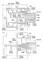
まず、本発明における撮像装置について、図1を用いて説明する。図1は撮像装置1の構成を示す模式図である。
First, an imaging apparatus according to the present invention will be described with reference to FIG. FIG. 1 is a schematic diagram illustrating a configuration of the
図1において、撮像装置1は、撮像部350と撮像回路300とで構成される。撮像部350は、撮像ユニット330と手振れ検知手段301とで構成される。撮像ユニット330は、レンズ211aとレンズ211bからなる撮像光学系211、撮像素子162および移動手段331で構成される。手振れ検知手段301は上下振れセンサ301P(Pitchの意)と左右振れセンサ301Y(Yawの意)とで構成される。ここに、撮像ユニット330、撮像光学系211および撮像素子162は、それぞれ、本発明における光学ユニット、光学系および光学素子である。
In FIG. 1, the
撮像回路300は、振れ検出回路303、手振れ補正手段305、AF手段167、アクチュエータ制御手段315、駆動回路部313、撮像制御部161、アナログデジタル(A/D)変換器163、画像処理部165、画像記録部181、操作部111および画像表示部131で構成される。駆動回路部313には昇圧回路が含まれ、移動手段331を構成する高分子アクチュエータを駆動するのに必要な電圧が作られる。
The imaging circuit 300 includes a
図1の撮像装置1は大きく2つの機能に分かれる。一つは撮像機能であり、他は撮像素子移動機能である。まず撮像機能について説明すると、被写体の像が撮像光学系211により撮像素子162の撮像面上に結像され、被写体像が撮像素子162により光電変換されて撮像データ162kとして出力される。出力された撮像データ162kはA/D変換器163でデジタルデータに変換され、画像処理部165でホワイトバランス処理やガンマ変換等の画像処理が施されて画像データ161gとして画像記録部181に記録されるとともに、画像表示部131に適宜表示される。これらの一連の撮像動作は撮像制御部161により制御される。
The
撮像素子移動機能は、さらに、撮像装置1の手振れを補正する手振れ補正機能と、撮像光学系211を合焦させるAF機能の2つの機能に分かれる。
The imaging element moving function is further divided into two functions: a camera shake correction function that corrects camera shake of the
手振れ補正機能は、手振れ検知手段301のセンサおよび振れ検出回路303により手振れが検知され、手振れ補正手段305により手振れ補正量が演算され、アクチュエータ制御手段315および駆動回路部313により移動手段331を構成する高分子アクチュエータに電圧が印加されて、撮像素子162が上下方向(以後、P方向と言う)および左右方向(以後、Y方向と言う)に移動されて手振れが補正される。
In the camera shake correction function, a camera shake is detected by the sensor of the camera
AF機能は、撮像素子162で撮像された画像のコントラストがAF手段167で算出され、画像のコントラストが最大となるように、アクチュエータ制御手段315および駆動回路部313により移動手段331を構成する高分子アクチュエータに電圧が印加されることで撮像素子162が光軸200方向(以後、F方向と言う)に移動され、撮像光学系211が合焦される。ここに、AF手段167は本発明におけるフォーカス検知手段として機能する。移動手段331については、図3以降で詳述する。
In the AF function, the contrast of the image captured by the
次に、本発明で使用される高分子アクチュエータの動作原理について、図2を用いて説明する。図2は、高分子アクチュエータの動作原理を説明するための模式図で、図2(a)は誘電ポリマ型の高分子アクチュエータの例を、図2(b)はイオン伝導型の高分子アクチュエータの例を示す。 Next, the operation principle of the polymer actuator used in the present invention will be described with reference to FIG. 2A and 2B are schematic diagrams for explaining the operation principle of the polymer actuator. FIG. 2A is an example of a dielectric polymer type polymer actuator, and FIG. 2B is an ion conduction type polymer actuator. An example is shown.
図2(a)において、誘電ポリマ型の高分子アクチュエータ401は、誘電ポリマ(シリコン樹脂やアクリル系樹脂)からなる伸張部403と、伸張部403の両面に設けられる導電性の炭素粒子を混ぜた高分子材料の電極405とからなる。電極405間に電界Eが印加されると、電極間に静電吸引力が発生して電極間が吸引され、その結果、弾性体である誘電ポリマからなる伸張部403が図の矢印の方向に伸張し、伸張の大きさは印加される電界Eの大きさに略比例する。
In FIG. 2A, a dielectric polymer
電極405を部分電極とすると部分電極の直下の伸張部403だけが伸張するので、電極405を複数の部分電極に分割し、それぞれを別個に駆動することで、複数個の高分子アクチュエータを並べた所謂アクチュエータアレイを作成可能である。高分子アクチュエータは、発生力が大きい、軽い、音がしない、低電力で駆動できる、材料が樹脂であるため成形で自由な形状が作れるなどの特徴がある。
If the
図2(b)において、イオン伝導型の高分子アクチュエータ411は、イオン交換樹脂413aからなる薄板413の両面に金電極415を化学メッキにより形成したものである。イオン交換樹脂413a内には陽イオン413bおよび極性分子413cが分散されており、電界の印加によりイオン交換樹脂413a内の陽イオン413bが陰極側へ移動し、薄板の表裏で膨潤に差が生じて変形し、曲がりを生じる。従って、電界の方向を逆にすると逆方向に曲がる。
In FIG. 2B, an ion conduction
本発明の第1乃至第3の実施の形態においては、誘電ポリマ型の高分子アクチュエータであってもイオン伝導型の高分子アクチュエータであっても適用が可能であるので、説明は誘電ポリマ型の高分子アクチュエータで行う。なお、第4および第5の実施の形態では、誘電ポリマ型の高分子アクチュエータが適用可能である。 The first to third embodiments of the present invention can be applied to either a dielectric polymer type polymer actuator or an ion conduction type polymer actuator. Perform with polymer actuator. In the fourth and fifth embodiments, a dielectric polymer type polymer actuator can be applied.
次に、上述した高分子アクチュエータ401を用いた移動手段331の第1の実施の形態について、図3乃至図6を用いて説明する。本第1の実施の形態は、撮像素子162をF方向に移動させることでオートフォーカス機能を実現する例である。
Next, a first embodiment of the moving means 331 using the
図3は、移動手段331の第1の実施の形態に用いられる高分子アクチュエータ401の構成を示す模式図で、図3(a)は高分子アクチュエータ401の上面図、図3(b)は高分子アクチュエータ401の図3(a)のA−A’での断面図、図3(c)は高分子アクチュエータ401の裏面図である。
3A and 3B are schematic views showing the configuration of the
図3(a)において、高分子アクチュエータ401の上面には3つの変位部401f1、401f2、401f3の3つの部分電極405aと外部取り出しのためのコネクタ端子407cおよびそれらを1本につなぐ配線407hが設けられている。
In FIG. 3A, on the upper surface of the
また、上述した3つの部分電極405aと外部取り出しのためのコネクタ端子407cおよびそれらを1本につなぐ配線407h以外の部分に、撮像素子162のリード端子(ここでは撮像素子162が10ピンであると仮定して図示している)と接続される10個のリードパターン409tと外部取り出しのための10個のコネクタ端子409cおよびそれらをつなぐ10本の配線409hとが設けられ、計11個のコネクタ端子407cおよび409cがコネクタ部401CNに取り出されている。
In addition, the lead terminal of the image sensor 162 (here, the
図3(b)において、高分子アクチュエータ401の伸張部403には3カ所の突起状の変位部401f1、401f2、401f3が一体的に形成されており、変位部401f1、401f2、401f3を挟み込む形で高分子アクチュエータ401の両面に設けられた部分電極405aと405bの間に電界Eが印加されることで、突起状の変位部401f1、401f2、401f3が、図に矢印で示した方向に伸張する。
In FIG. 3B, three protrusion-like displacement portions 401f1, 401f2, 401f3 are integrally formed on the extending
高分子アクチュエータ401の発生力は静電力、つまり電極間の距離に依存するため、3カ所の突起状の変位部401f1、401f2、401f3の裏面は凹形状にされており、変位部の厚みが均一にされている。説明を分かりやすくするために、図には部分電極405aと405bのみを示しており、断面から見える他の配線部分については図示していない。
Since the generated force of the
図3(c)において、高分子アクチュエータ401の裏面には、二等辺三角形の各頂点の位置に3つの変位部401f1、401f2、401f3が設けられ、これら3つの変位部401f1、401f2、401f3の3つの部分電極405bと外部取り出しのための3つのコネクタ端子408cおよびそれらをつなぐ3本の配線408hとが設けられ、3つのコネクタ端子408cがコネクタ部401CNに取り出されている。
In FIG. 3C, on the back surface of the
図4は、移動手段331を構成する可動部333の構成を示す模式図で、図4(a)は上面図、図4(b)は図4(a)のA−A’での断面図、図4(c)は裏面図である。
4A and 4B are schematic views showing the configuration of the
図4(a)において、図3で説明した高分子アクチュエータ401のリードパターン409tが形成された側の面に撮像素子162が搭載され、撮像素子162のリード端子162cと高分子アクチュエータ401上のリードパターン409tとが例えば導電性接着剤等で接続されることで、撮像素子162を構成する撮像素子チップ162bの内部回路と接続された10本のリード端子162cがコネクタ部401CNに取り出される。コネクタ部401CNには、高分子アクチュエータ401の3つの変位部401f1、401f2、401f3の部分電極405aもコネクタ端子407cとして取り出されている。
4A, the
図4(b)および(c)において、高分子アクチュエータ401と撮像素子162とは、フレーム333a上に搭載され、フレーム333aとフレーム333aの係止部333bおよび333cとで挟み込まれている。フレーム333aには高分子アクチュエータ401の3つの変位部401f1、401f2、401f3の位置に開口部333hが開けられ、3つの変位部401f1、401f2、401f3が開口部333hから突出するように構成されている。
4B and 4C, the
高分子アクチュエータ401の平面部401aは、撮像素子パッケージ162aとフレーム333aとに挟まれ、平面部401a上にある配線部分に電界Eが印加されても伸張できないように規制されている。コネクタ部401CNには、例えばフレキシブル基板902と接続されたコネクタ901が差し込まれて電気的に接続され、撮像素子162および高分子アクチュエータ401と撮像回路300とが接続される。コネクタ部401CNのコネクタ端子407cおよび409cとフレキシブル基板902とを、例えば導電性接着剤で接着してもよい。
The
図5は、移動手段331の第1の実施の形態の構成を示す模式図で、図5(a)は上面図、図5(b)は図5(a)のB−B’での断面図である。
FIGS. 5A and 5B are schematic views showing the configuration of the moving
図5(a)において、図4で説明した可動部333は、固定部331aの内部に挿入され、固定部331aの内壁に設けられた5カ所の突起部331dによってP方向およびY方向の移動が規制される。
In FIG. 5A, the
図5(b)において、可動部333を構成する高分子アクチュエータ401の3つの変位部401f1、401f2、401f3は固定部331aの底面に接している。可動部333は付勢バネ331cにより−F方向に付勢されており、高分子アクチュエータ401の3つの変位部401f1、401f2、401f3の部分電極405aと405bとの間に電界Eが印加されることで3つの変位部401f1、401f2、401f3が伸張し、付勢バネ331cの力に抗して可動部333を光軸200の方向、つまりF方向に移動させる。
In FIG. 5B, the three displacement parts 401f1, 401f2, 401f3 of the
固定部331aの可動部333のコネクタ部401CNに対面する部分には開口部331hが開けられており、例えばフレキシブル基板902と接続されたコネクタ901が差し込まれて、コネクタ部401CNと電気的に接続される。
An
図6は、上述した3つの変位部401f1、401f2、401f3に印加される電界Eと撮像素子162のF方向変位の関係を示すタイミングチャートである。
FIG. 6 is a timing chart showing the relationship between the electric field E applied to the three displacement units 401f1, 401f2, and 401f3 described above and the displacement in the F direction of the
図6において、タイミングT1で3つの変位部401f1、401f2、401f3に+Eの電界が印加されると、3つの変位部401f1、401f2、401f3が付勢バネ331cの付勢力に抗して伸張し、撮像素子162の撮像素子パッケージ162aが+F方向に押され、撮像素子162は+F方向に変位する。
In FIG. 6, when an electric field of + E is applied to the three displacement portions 401f1, 401f2, 401f3 at timing T1, the three displacement portions 401f1, 401f2, 401f3 expand against the urging force of the urging
同様に、タイミングT2で3つの変位部401f1、401f2、401f3に印加されている電界が解除されると、3つの変位部401f1、401f2、401f3が伸張状態から元の形状に戻り、撮像素子162の撮像素子パッケージ162aが付勢バネ331cの付勢力により−F方向に押し戻され、撮像素子162は−F方向に変位して元の位置に戻る。
Similarly, when the electric fields applied to the three displacement portions 401f1, 401f2, 401f3 are released at timing T2, the three displacement portions 401f1, 401f2, 401f3 return to their original shapes from the expanded state, and the
また、3つの変位部401f1、401f2および401f3に印加する電界Eを個々に細かく制御することで、光軸200に対する撮像素子162の撮像面の傾きを補正したり、逆に傾きを持たせて像面を傾けることで、チルト撮影のような特殊効果を持たせたりすることも可能となる。
Further, by individually finely controlling the electric field E applied to the three displacement parts 401f1, 401f2, and 401f3, the inclination of the imaging surface of the
以上に示したように、本第1の実施の形態によれば、撮像素子162を光軸200方向に移動させることによりオートフォーカス機能を実現するための高分子アクチュエータ401を設け、高分子アクチュエータ401の変位部以外の部分に撮像素子162の端子の配線を設けることにより、可動部333上に撮像素子を搭載する基板が不要になり、移動手段331の小型化、軽量化、低価格化に寄与する。
As described above, according to the first embodiment, the
さらに、高分子アクチュエータ401は、3つの変位部401f1、401f2、401f3を一体的に形成でき、撮像素子162と移動手段331の保持部331aの間の僅かの隙間に配置することができてスペース効率が非常によく、駆動も単に電界を印加するだけで非常に簡単で制御もしやすい。
Further, the
次に、高分子アクチュエータ401を用いた移動手段331の第2の実施の形態を、図7乃至図9を用いて説明する。本第2の実施の形態は、撮像素子162をP方向およびY方向に移動させることで手振れ補正機能を実現する例である。
Next, a second embodiment of the moving means 331 using the
図7は、移動手段331の第2の実施の形態に用いられる高分子アクチュエータ401の構成を示す模式図で、図7(a)は高分子アクチュエータ401の上面図、図7(b)は高分子アクチュエータ401の裏面図である。
7A and 7B are schematic views showing the configuration of the
図7(a)において、図3(a)と同様に、高分子アクチュエータ401の上面には5つの変位部401p1、401p2、401y1、401y2、401y3の5つの部分電極405aと外部取り出しのためのコネクタ端子407cおよびそれらを1本につなぐ配線407hが設けられている。図3(b)に示したと同様に、変位部の厚みを均一にするために、5つの変位部は凹形状にされている。
7A, similarly to FIG. 3A, the upper surface of the
また、上述した5つの部分電極405aと外部取り出しのためのコネクタ端子407cおよびそれらを1本につなぐ配線407h以外の部分に、撮像素子162のリード端子(ここでは撮像素子162が10ピンであると仮定して図示している)162cと接続される10個のリードパターン409tと外部取り出しのための10個のコネクタ端子409cおよびそれらをつなぐ10本の配線409hとが設けられ、計11個のコネクタ端子407cおよび409cがコネクタ部401CNに取り出されている。
Further, the lead terminal of the image sensor 162 (in this case, the
高分子アクチュエータ401は、図に破線で示した部分で周囲がリードパターン409tのある側に折り曲げられ、図の右側にコネクタ部401CNが飛び出した箱形にされる。
The
図7(b)において、図3(c)と同様に、高分子アクチュエータ401の裏面の、図に破線で示した部分で折り曲げられた場合の箱形の側面になる部分に、5つの変位部401p1、401p2、401y1、401y2、401y3が設けられ、これら5つの変位部401p1、401p2、401y1、401y2、401y3の5つの部分電極405bと外部取り出しのための5つのコネクタ端子408cおよびそれらをつなぐ5本の配線408hとが設けられ、5つのコネクタ端子408cがコネクタ部401CNに取り出されている。
In FIG. 7B, as in FIG. 3C, there are five displacement portions on the back surface of the
図8は、移動手段331の第2の実施の形態の構成を示す模式図で、図8(a)は図8(b)のD−D’での断面図、図8(b)は図8(a)のC−C’での断面図である。
FIG. 8 is a schematic diagram showing the configuration of the second embodiment of the moving
図8(a)において、移動手段331を構成する可動部333は、固定部331aの内部に挿入されている。可動部333を構成する高分子アクチュエータ401は、図7(a)に示した破線部で折り曲げられて、可動部を構成するフレーム333aの内部に挿入され、フレーム333aとフレーム333aに固定された規制部材333bとの間に挟み込まれている。撮像素子162は規制部材333bの内側に挿入されており、そのリード端子162cは、高分子アクチュエータ401のリードパターン409tに例えば導電性接着剤等で接続されており、撮像素子162の10本のリード端子162cがコネクタ部401CNに取り出されている。
In FIG. 8A, the
高分子アクチュエータ401の5つの変位部401p1、401p2、401y1、401y2、401y3は、フレーム333aに開けられた開口部333hから可動部333の外側に向けて突出し、固定部331aの内壁に接している。5つの変位部401p1、401p2、401y1、401y2、401y3に印加する電界を制御することで、撮像素子162がP方向およびY方向に移動され、あるいは光軸200の周り(以後、R方向と言う)に回転される。
The five displacement portions 401p1, 401p2, 401y1, 401y2, 401y3 of the
ここで、R方向の動作について説明すると、図8(a)の例えばY方向の3個の変位部のうち左部の変位部401y1と右下部の変位部401y3には電界が印加されず、右上部の変位部401y2電界Eが印加されて伸張することで、可動部333は変位部401y2により図の右上から左方向の力を受け、図の面内で反時計方向に回転する。この時、左部の変位部401y1と右下部の変位部401y3とは可動部333の反時計方向の回転に伴って変形する。
Here, the operation in the R direction will be described. Of the three displacement parts in the Y direction in FIG. 8A, for example, no electric field is applied to the left displacement part 401y1 and the lower right displacement part 401y3. When the electric field E is applied to the displacement portion 401y2 and expands, the
図8(b)において、フレーム333aの底面は固定部331aの内側底面に接している。固定部331aの可動部333のコネクタ部401CNに対面する部分には開口部331hが開けられており、図5と同様に、例えば図示しないフレキシブル基板902と接続されたコネクタ901が差し込まれて、コネクタ部401CNと電気的に接続される。
In FIG. 8B, the bottom surface of the
図9は、上述した5つの変位部401p1、401p2、401y1、401y2、401y3に印加される電界Eと撮像素子162のP方向、Y方向の変位およびR方向の回転の関係を示すタイミングチャートである。
FIG. 9 is a timing chart showing the relationship between the electric field E applied to the five displacement portions 401p1, 401p2, 401y1, 401y2, and 401y3 described above and the displacement of the
図9において、タイミングT11でP方向の変位部401p1に電界Eが印加されることで、撮像素子162は−P方向に移動する。タイミングT12でP方向の変位部401p2に電界Eが印加されることで、撮像素子162は+P方向に移動する。
In FIG. 9, when the electric field E is applied to the displacement portion 401p1 in the P direction at timing T11, the
タイミングT13でY方向の変位部401y1に電界Eが印加されることで、撮像素子162は+Y方向に移動する。タイミングT14でY方向の変位部401y2と401y3に電界Eが印加されることで、撮像素子162は−Y方向に移動する。
When the electric field E is applied to the displacement portion 401y1 in the Y direction at the timing T13, the
タイミングT15でY方向の変位部401y3に電界Eが印加されることで、撮像素子162はR方向の時計方向に回転する。タイミングT16でY方向の変位部401y2に電界Eが印加されることで、撮像素子162はR方向の反時計方向に回転する。
When the electric field E is applied to the displacement portion 401y3 in the Y direction at timing T15, the
以上に示したように、本第2の実施の形態によれば、撮像素子162を光軸200に垂直な面内で移動させることにより手振れ補正機能を実現するための高分子アクチュエータ401を設け、高分子アクチュエータ401の変位部以外の部分に撮像素子162の端子の配線を設けることにより、可動部333上に撮像素子を搭載する基板が不要になり、移動手段331の小型化、軽量化、低価格化に寄与する。
As described above, according to the second embodiment, the
さらに、高分子アクチュエータ401は、5つの変位部401p1、401p2、401y1、401y2、401y3を一体的に形成でき、撮像素子162と移動手段331の保持部331aの間の僅かの隙間に配置することができてスペース効率が非常によく、駆動も単に電界を印加するだけで非常に簡単で制御もしやすい。
Furthermore, the
次に、高分子アクチュエータ401を用いた移動手段331の第3の実施の形態を、図10および図11を用いて説明する。本第3の実施の形態は、撮像素子162をP方向、Y方向およびF方向に移動させることで手振れ補正機能とオートフォーカス機能とを実現する、つまり第1の実施の形態と第2の実施の形態とを両立させる例である。
Next, a third embodiment of the moving means 331 using the
図10は、移動手段331の第3の実施の形態に用いられる高分子アクチュエータ401の構成を示す模式図で、図10(a)は高分子アクチュエータ401の上面図、図10(b)は高分子アクチュエータ401の裏面図である。
FIG. 10 is a schematic diagram showing the configuration of the
図10(a)において、高分子アクチュエータ401の上面には、図3と図7とを合わせた8つの変位部401f1、401f2、401f3、401p1、401p2、401y1、401y2、401y3の8つの部分電極405aと外部取り出しのためのコネクタ端子407cおよびそれらを1本につなぐ配線407hが設けられている。
In FIG. 10A, on the upper surface of the
また、図3および図7と同様に、撮像素子162のリード端子162cと接続される10個のリードパターン409tと外部取り出しのための10個のコネクタ端子409cおよびそれらをつなぐ10本の配線409hも設けられており、計11個のコネクタ端子407cおよび409cがコネクタ部401CNに取り出されている。ここでも、図3(b)に示したと同様に、変位部の厚みを均一にするために、8つの変位部は凹形状にされている。
3 and 7, ten
図10(b)においても、図3と図7とを合わせた形で、8つの変位部401f1、401f2、401f3、401p1、401p2、401y1、401y2、401y3が設けられ、これら8つの変位部401f1、401f2、401f3、401p1、401p2、401y1、401y2、401y3の8つの部分電極405bと外部取り出しのための8つのコネクタ端子408cおよびそれらをつなぐ8本の配線408hとが設けられ、8つのコネクタ端子408cがコネクタ部401CNに取り出されている。
Also in FIG. 10 (b), eight displacement portions 401f1, 401f2, 401f3, 401p1, 401p2, 401y1, 401y2, 401y3 are provided in a form combining FIG. 3 and FIG. 7, and these eight displacement portions 401f1, There are provided eight
図11は、移動手段331の第3の実施の形態の構成を示す模式図で、図5(a)のB−B’での断面および図8(a)のC−C’での断面と同様の断面図である。
FIG. 11 is a schematic diagram showing the configuration of the third embodiment of the moving
図11において、可動部333を構成する高分子アクチュエータ401の8つの変位部401f1、401f2、401f3、401p1、401p2、401y1、401y2、401y3は、可動部333を構成するフレーム333aに開けられた開口部333hから可動部333の外側に向けて突出しており、F方向の3つの変位部401f1、401f2、401f3は固定部331aの底面に接し、P方向およびY方向の5つの変位部401p1、401p2、401y1、401y2、401y3は固定部331aの内壁側面に接している。
In FIG. 11, eight displacement portions 401
可動部333は付勢バネ331cにより−F方向に付勢されており、高分子アクチュエータ401のF方向の3つの変位部401f1、401f2、401f3の部分電極405aと405bとの間に電界Eが印加されることで3つの変位部401f1、401f2、401f3が伸張し、付勢バネ331cの付勢力に抗して可動部333がF方向に移動される。高分子アクチュエータ401の駆動方法は、図6に示したものと同じである。
The
また、P方向およびY方向の5つの変位部401p1、401p2、401y1、401y2、401y3の部分電極405aと405bとの間に電界Eが印加されることで、撮像素子162がP方向およびY方向に移動され、あるいは光軸200の周り(以後、R方向と言う)に回転される。高分子アクチュエータ401の駆動方法は、図9に示したものと同じである。
In addition, the electric field E is applied between the
固定部331aの可動部333のコネクタ部401CNに対面する部分には開口部331hが開けられており、例えばフレキシブル基板902と接続されたコネクタ901が差し込まれて、コネクタ部401CNと電気的に接続される。
An
以上に示したように、本第3の実施の形態によれば、撮像素子162を光軸200方向に移動させることによりオートフォーカス機能を実現するための高分子アクチュエータ401と、撮像素子162を光軸200に垂直な面内で移動させることにより手振れ補正機能を実現するための高分子アクチュエータ401とを一体に形成し、かつ、高分子アクチュエータ401の変位部以外の部分に撮像素子162の端子の配線を設けることにより、可動部333上に撮像素子を搭載する基板が不要になり、移動手段331の小型化、軽量化、低価格化に寄与する。
As described above, according to the third embodiment, the
さらに、高分子アクチュエータ401は、撮像素子162と移動手段331の保持部331aの間の僅かの隙間に配置することができてスペース効率が非常によく、駆動も単に電界を印加するだけで非常に簡単で制御もしやすい。
Furthermore, the
次に、高分子アクチュエータ401を用いた移動手段331の第4の実施の形態について、図12および図13を用いて説明する。本第4の実施の形態は、撮像素子162をF方向に移動させることでオートフォーカス機能を実現する例である。
Next, a fourth embodiment of the moving means 331 using the
図12は、第4の実施の形態における高分子アクチュエータ401の構成を示す模式図で、図12(a)は高分子アクチュエータ401の上面図、図12(b)および(c)は高分子アクチュエータ401の図12(a)のD−D’断面図で、図12(b)は電極間に電界が印加されていない状態を、図12(c)は電界が印加されている状態を示す。
FIG. 12 is a schematic diagram showing a configuration of a
図12(a)において、高分子アクチュエータ401は、周辺の平坦部491aと台形状に盛り上がった中央部の台形上部491bおよび斜面部491cとからなり、斜面部491cの表裏両面にはそれぞれ部分電極405aおよび405bが設けられている。平坦部491aと台形上部491bには部分電極405aおよび405bが設けられていないので、平坦部491aと台形上部491bとは部分電極405aおよび405bへの電界の印加によっては変形せず、アクチュエータとしては機能しない。
In FIG. 12 (a), the
台形上部491bの台形表面側には、撮像素子162のリード端子162cと接続されるリードパターン409tが、本例では10個設けられている。さらに、台形上部491bには、撮像素子162を台形上部491b上に固定してリード端子162cとリードパターン409tとを導通させるための後述する圧着部材492を通すための貫通穴492cが、本例では4個設けられている。
Ten
斜面部491cの台形表面側には、リードパターン409tとコネクタ端子409cとを接続する10本の配線409hが配置され、配線409hが通るスペース以外は、配線409hと接触しない最低限の間隔をあけて部分電極405aが設けられている。斜面部491cの台形裏面側には、部分電極405bが斜面全面に設けられている。本例では10本の配線409hは図の左右の斜面部491cにのみ設けられているが、四方に分散して設けられてもよい。斜面部491cの部分電極405aと405bとに挟まれた部分が本発明の変位部に相当する。
Ten
平坦部491aの図の表面側には、リードパターン409tと接続された10個のコネクタ端子409c、斜面部491c上の部分電極405aを接続する配線408hとそれに接続された2個のコネクタ端子408cおよび斜面部491cの台形裏面側の部分電極405bに接続された2個のコネクタ端子407cが設けられている。部分電極405bとコネクタ端子407cとは例えば平坦部491aに設けられたスルーホール等で接続される。本例では部分電極405bに接続されたコネクタ端子407cを2個設けてあるが、構成的には最低限1個あればよい。
On the surface side of the
また、平坦部491aには、コネクタ端子409c,408cおよび407cと後述するフレキシブル基板902とを接続するためのビス穴493が、本例では4個設けられている。
The
図12(b)において、斜面部491cは平坦部491aと台形上部491bとを繋ぐヒンジ部であり、その表裏両面にそれぞれ部分電極405aと405bとが設けられている。部分電極405aと405bとの間に電界が印加されると、部分電極405aと405bとが引き合い、電極間の伸張部403が変形することで斜面部491cが伸張し、結果として、図12(c)に示すように、平坦部491aから台形上部491bを図の矢印Ar方向に押し上げる。
In FIG. 12B, a
この時、部分電極405a、405bおよび配線409hは、例えば高分子アクチュエータ401と同様の導電性の炭素粒子を混ぜた高分子材料で構成されており、斜面部491cの伸張に応じて伸張するので、断線の心配はない。
At this time, the
図13は、移動手段331の第4の実施の形態の構成を示す模式図で、図13(a)は移動手段331の上面図、図13(b)および(c)は移動手段331の図13(a)のE−E’断面図で、図13(b)は電極間に電界が印加されていない状態を、図13(c)は電界が印加されている状態を示す。
FIG. 13 is a schematic diagram showing the configuration of the fourth embodiment of the moving
図13(a)において、図12で示した高分子アクチュエータ401の台形上部491b上には、撮像素子162が搭載され、圧着部材492の圧着枠492aで上から押さえ込まれている。また、平坦部491a上のコネクタ端子409c,408cおよび407cと、フレキシブル基板902とが、圧接板903を介してビス止めされて接続されている。
In FIG. 13A, an
図13(b)において、台形上部491bの台形裏面側には、圧着板492bが密着されている。圧着枠492aの先端の爪部は、貫通穴492cおよび圧着板492bに設けられた穴を通って圧着板492bの裏面に達して圧着板492bに係止され、圧着枠492aと圧着板492bとで撮像素子162と台形上部491bとを挟み込んでいる。これによって、撮像素子162のリード端子162cと台形上部491bのリードパターン409tとが電気的に接続される。
In FIG. 13B, a crimping
平坦部491a上のコネクタ端子409c,408cおよび407cと、フレキシブル基板902とは、圧接板903を介して固定部331aにビス止めされ、電気的に接続されている。
The
高分子アクチュエータ401の斜面部491cの表裏に設けられた部分電極405aと405bとの間に電界が印加されると、部分電極405aと405bとが引き合い、電極間の伸張部403が変形することで斜面部491cが伸び、結果として、図13(c)に示すように、撮像素子162を図の矢印Ar方向に押し上げる。
When an electric field is applied between the
以上に述べたように、本発明の第4の実施の形態によれば、変形しない平坦部491aと台形上部491bとの間にヒンジ部である斜面部491cを設け、斜面部491cの表裏両面に部分電極405aおよび405bを設けることで、部分電極405aと405bとの間に印加される電界によって台形上部491bを平坦部491aから押し上げることができる。そして、台形上部491b上に撮像素子162を搭載することで撮像素子162をF方向に移動させることができ、オートフォーカス機能を実現することができる。
As described above, according to the fourth embodiment of the present invention, the
さらに、斜面部491c上の部分電極405aを部分的に切り欠いて、切り欠き部分にリードパターン409tとコネクタ端子409cとを接続する配線409hを通すことで、台形上部491b上に撮像素子を搭載する基板が不要になり、移動手段331の小型化、軽量化、低価格化に寄与する。
Further, the
なお、斜面部491c上に配線409hを通すことで、配線409hが通る部分については、部分電極405aと405b間の電界の印加によって変形しない。従って、斜面部491cの配線409hが通っている部分と通っていない部分とでは変形率が異なる。よって、例えば本例のように撮像素子の傾きの発生が問題となるケースでは、本例に示したように、配線409hを斜面部491cの対向する面に分散させ、配線409h間の斜面部491cにも部分電極405aを設ける等の配慮が行われることが望ましい。
Note that by passing the
また、配線409hは斜面部491cの伸張に従って伸張するため、斜面部491cの伸張によって抵抗値が変化する。ただしその変化は微小であり、撮像素子162の特性に影響を与えることはない。
Further, since the
次に、上述した高分子アクチュエータ401を用いた移動手段331の第5の実施の形態について、図14および図15を用いて説明する。本第5の実施の形態は、オートフォーカスで使用される補助光ユニットにおいて、発光素子をF方向に移動させることで補助光のピント調節機能を実現する例である。
Next, a fifth embodiment of the moving means 331 using the
図14は、第5の実施の形態における高分子アクチュエータ401の構成を示す模式図で、図14(a)は高分子アクチュエータ401の発光素子搭載面のパターン図、図14(b)は高分子アクチュエータ401を図14(a)の矢印E方向から見た側面図である。
14A and 14B are schematic views showing the configuration of the
図14(a)において、高分子アクチュエータ401は、周辺の平坦部491aと台形状に窪んだ中央部の台形底部491dおよび斜面部491cとからなる。図12とは異なり、斜面部491cは図の左右のみに設けられている。斜面部491cの表裏両面にはそれぞれ部分電極405aおよび405bが設けられている。平坦部491aと台形底部491dには部分電極405aおよび405bが設けられていないので、平坦部491aと台形底部491dとは部分電極405aおよび405bへの電界の印加によっては変形せず、アクチュエータとしては機能しない。
14A, the
台形底部491dの発光素子搭載面には、後述する発光素子998のリード端子と接続されるリードパターン409tが、本例では2個設けられている。斜面部491cの発光素子搭載面側には、上述したリードパターン409tと平坦部491a上に設けられたコネクタ端子409cとを接続する2本の配線409hが配置されている。
In the present example, two
斜面部491cの配線409hが通るスペース以外の部分には、部分電極405aが設けられている。ただし、図12とは異なり、2本の配線409hの間には部分電極405aは設けられていない。斜面部491cの発光素子搭載面の裏面には、部分電極405bが斜面全面に設けられている。2本の配線409hは図の左方向の斜面部491cにまとめて設けられている。
A
平坦部491aの発光素子搭載面側には、リードパターン409tと接続された2個のコネクタ端子409c、斜面部491c上の部分電極405aに接続されたコネクタ端子408cおよび斜面部491cの発光素子搭載面の裏面側の部分電極405bに接続されたコネクタ端子407cが設けられている。部分電極405bとコネクタ端子407cとは例えば平坦部491aに設けられたスルーホール等で接続される。
On the light emitting element mounting surface side of the
図14(b)において、斜面部491cは平坦部491aと台形底部491dとを繋ぐヒンジ部であり、その表裏両面にそれぞれ部分電極405aと405bとが設けられている。部分電極405aと405bとの間に電界が印加されると、部分電極405aと405bとが引き合い、電極間の伸張部403が変形することで斜面部491cが伸張し、結果として平坦部491aから台形上部491bを図の矢印Ar方向に押し下げる。
In FIG. 14B, the
この時、部分電極405a、405bおよび配線409hは、例えば高分子アクチュエータ401と同様の導電性の炭素粒子を混ぜた高分子材料で構成されており、斜面部491cの伸張に応じて伸張するので、断線の心配はない。
At this time, the
図15は、移動手段331の第5の実施の形態の構成を示す模式図で、図15(a)は移動手段331の発光素子搭載面を示す図、図15(b)および(c)は移動手段331の図15(a)の矢印E方向から見た側面図で、図15(b)は電極間に電界が印加されていない状態を、図15(c)は電界が印加されている状態を示す。
FIG. 15 is a schematic diagram showing the configuration of the fifth embodiment of the moving
図15(a)において、図14で示した高分子アクチュエータ401の台形底部491d上には、発光素子998が搭載され、発光素子998上にはパターンマスク997が配置されている。発光素子998とパターンマスク997とは、圧着部材492でクリップで挟むようにして台形底部491dに圧接されている。平坦部491a上のコネクタ端子409c,408cおよび407cは、例えば図示しないコネクタ等によりフレキシブル基板等と接続される。
In FIG. 15A, a
図15(b)において、補助光ユニット999は、投光レンズ211、移動手段331、発光素子998およびパターンマスク997等で構成される。発光素子998、パターンマスク997および台形底部491dとは圧着部材492で挟みこまれ、これによって、発光素子998のリード端子と台形底部491dのリードパターン409tとが電気的に接続されている。平坦部491aは、図示しない固定部材によって投光レンズ211との位置関係が所定の状態となるように固定されている。
In FIG. 15B, the auxiliary
これによって、発光素子998が照明光源となってパターンマスク997上のパターンを投光レンズ211を介して被写体上に投影することができ、オートフォーカス時の補助光を実現することができる。図15(b)は部分電極405aと405bとの間に電界が印加されていない状態であり、この時にはパターンマスク997は無限遠にピントがあっている。ここに、補助光ユニット999、発光素子998および投光レンズ211は、それぞれ、本発明における光学ユニット、光学素子および光学系である。
As a result, the
高分子アクチュエータ401の斜面部491cの表裏に設けられた部分電極405aと405bとの間に電界が印加されると、部分電極405aと405bとが引き合い、電極間の伸張部403が変形することで斜面部491cが伸び、結果として、図15(c)に示すように、発光素子997を図の矢印Ar方向に押し下げる。この時、パターンマスク997は近距離側にピントが合う状態となる。
When an electric field is applied between the
以上に述べたように、本発明の第5の実施の形態によれば、変形しない平坦部491aと台形底部491dとの間にヒンジ部である斜面部491cを設け、斜面部491cの表裏両面に部分電極405aおよび405bを設けることで、部分電極405aと405bとの間に印加される電界によって台形底部491dを平坦部491aから押し下げることができる。そして、台形底部491d上に発光素子998を搭載することで、オートフォーカス時の補助光を実現することができる。
As described above, according to the fifth embodiment of the present invention, the
さらに、斜面部491c上の部分電極405aを部分的に切り欠いて、切り欠き部分にリードパターン409tとコネクタ端子409cとを接続する配線409hを通すことで、台形底部491d上に発光素子998を搭載する基板が不要になり、移動手段331の小型化、軽量化、低価格化に寄与する。
Further, the
なお、第4の実施の形態と同様に、斜面部491c上に配線409hを通すことで、斜面部491cの配線409hが通っている部分と通っていない部分とでは変形率が異なる。しかし、例えば本例のように発光素子998の傾きがあまり大きな問題とならないケースでは、配線409hを斜面部491cの一方の面に集中させても問題ないし、配線409h間の斜面部491cに部分電極405aを設ける必要もない。
As in the fourth embodiment, by passing the
また、配線409hは斜面部491cの伸張に従って伸張するため、斜面部491cの伸張によって抵抗値が変化する。ただしその変化は微小であり、発光素子998の特性に影響を与えることはない。
Further, since the
以上に述べたように、本発明によれば、高分子アクチュエータを備え、該アクチュエータを用いて光学素子を移動させることで「オートフォーカス機能」や「手振れ補正機能」を実現し、かつ高分子アクチュエータに光学素子の電気配線を設けることで光学素子の電気配線に用いられる基板を削減することにより、組立性がよく小型で高性能で低価格な光学ユニットおよび撮像装置を提供することができる。 As described above, according to the present invention, a polymer actuator is provided, and an “autofocus function” and a “camera shake correction function” are realized by moving an optical element using the actuator. By providing the electrical wiring of the optical element to the substrate, the number of substrates used for the electrical wiring of the optical element can be reduced, thereby providing an optical unit and an imaging apparatus that are easy to assemble, small in size, high in performance, and low in price.
尚、本発明に係る光学ユニットおよび撮像装置を構成する各構成の細部構成および細部動作に関しては、本発明の趣旨を逸脱することのない範囲で適宜変更可能である。 The detailed configuration and detailed operation of each component constituting the optical unit and the imaging apparatus according to the present invention can be changed as appropriate without departing from the spirit of the present invention.
1 撮像装置
111 操作部
131 画像表示部
161 撮像制御部
162 撮像素子
162b 撮像素子チップ
163 アナログデジタル(A/D)変換器
165 画像処理部
167 AF手段
181 画像記録部
200 光軸
201 鏡胴
211 撮像光学系
211a レンズ
211b レンズ
300 撮像回路
301 手振れ検知手段
303 振れ検出回路
305 手振れ補正手段
313 駆動回路部
315 アクチュエータ制御手段
330 撮像ユニット
331 移動手段
331a 固定部
331b 規制部材
331c 付勢バネ
331s 筋目
333 可動部
333b フレームの規制部材
335 第2のフレーム
335b 第2のフレームの規制部材
337 接着剤
350 撮像部
401 (誘電ポリマ型の)高分子アクチュエータ
401a 平面部
401b 変位部
401x 作用部
403 伸張部
405 電極
407c コネクタ端子
408c コネクタ端子
409c コネクタ端子
409h 配線
409t リードパターン
411 (イオン伝導型の)高分子アクチュエータ
413 薄板
413a イオン交換樹脂
413b 陽イオン
413c 極性分子
415 金電極
491a 平坦部
491b 台形上部
491c 斜面部
491d 台形底部
492 圧着部材
492a 圧着枠
492b 圧着板
492c 貫通穴
493 ビス穴
902 フレキシブル基板
903 圧接板
997 パターンマスク
998 発光素子
999 補助光ユニット
DESCRIPTION OF
Claims (7)
光学素子と、
前記光学素子を載置する基板として機能し、且つ、前記光学素子を移動させるための高分子アクチュエータとを有し、
前記高分子アクチュエータは、部分電極により局所的に変位してアクチュエータとして機能する複数の部分的変位部を有するアクチュエータアレイを形成し、前記部分的変位部以外の部分に、前記光学素子に接続される電気配線を設けたことを特徴とする光学ユニット。 Optical system,
An optical element;
It functions as a substrate on which the optical element is placed, and has a polymer actuator for moving the optical element,
The polymer actuator is locally displaced by a partial electrode to form an actuator array having a plurality of partial displacement portions that function as actuators, and is connected to the optical element at a portion other than the partial displacement portion An optical unit provided with electrical wiring.
前記光学ユニットが有する光学系で結像される被写体像のフォーカス状態を検出するフォーカス検知手段と、
前記フォーカス検知手段の検出結果に基づいて、前記光学ユニットが有する高分子アクチュエータにより前記撮像素子を前記光学系の光軸方向に移動させる移動手段とを有することを特徴とする撮像装置。 An optical unit according to claim 3 ,
Focus detection means for detecting a focus state of a subject image formed by the optical system of the optical unit;
An image pickup apparatus comprising: a moving unit that moves the image pickup element in an optical axis direction of the optical system by a polymer actuator included in the optical unit based on a detection result of the focus detection unit.
前記光学ユニットの手振れを検出する手振れ検知手段と、
前記手振れ検知手段の検知結果に基づいて、前記光学ユニットが有する高分子アクチュエータにより前記撮像素子を前記光学ユニットが有する光学系の光軸に垂直な方向に移動させる移動手段とを有することを特徴とする撮像装置。 An optical unit according to claim 3 ,
Camera shake detection means for detecting camera shake of the optical unit;
And moving means for moving the image sensor in a direction perpendicular to the optical axis of the optical system of the optical unit by a polymer actuator of the optical unit based on the detection result of the camera shake detection means. An imaging device.
前記光学ユニットが有する光学系で結像される被写体像のフォーカス状態を検出するフォーカス検知手段と、
前記光学ユニットの手振れを検出する手振れ検知手段と、
前記フォーカス検知手段の検出結果に基づいて、前記光学ユニットが有する高分子アクチュエータにより前記撮像素子を前記光学系の光軸方向に移動させ、前記手振れ検知手段の検知結果に基づいて前記高分子アクチュエータにより前記撮像素子を前記光学系の光軸に垂直な方向に移動させる移動手段とを有することを特徴とする撮像装置。 An optical unit according to claim 3 ,
Focus detection means for detecting a focus state of a subject image formed by the optical system of the optical unit;
Camera shake detection means for detecting camera shake of the optical unit;
Based on the detection result of the focus detection means, the image sensor is moved in the optical axis direction of the optical system by a polymer actuator of the optical unit, and based on the detection result of the camera shake detection means, An image pickup apparatus comprising: a moving unit that moves the image pickup element in a direction perpendicular to an optical axis of the optical system.
Priority Applications (2)
| Application Number | Priority Date | Filing Date | Title |
|---|---|---|---|
| JP2007127728A JP4972779B2 (en) | 2006-05-30 | 2007-05-14 | Optical unit and imaging device |
| US11/805,219 US8284263B2 (en) | 2006-05-30 | 2007-05-22 | Optical unit and image pickup apparatus having an optical device and a polymer actuator for moving the optical device |
Applications Claiming Priority (3)
| Application Number | Priority Date | Filing Date | Title |
|---|---|---|---|
| JP2006149538 | 2006-05-30 | ||
| JP2006149538 | 2006-05-30 | ||
| JP2007127728A JP4972779B2 (en) | 2006-05-30 | 2007-05-14 | Optical unit and imaging device |
Publications (2)
| Publication Number | Publication Date |
|---|---|
| JP2008011506A JP2008011506A (en) | 2008-01-17 |
| JP4972779B2 true JP4972779B2 (en) | 2012-07-11 |
Family
ID=38821527
Family Applications (1)
| Application Number | Title | Priority Date | Filing Date |
|---|---|---|---|
| JP2007127728A Expired - Fee Related JP4972779B2 (en) | 2006-05-30 | 2007-05-14 | Optical unit and imaging device |
Country Status (2)
| Country | Link |
|---|---|
| US (1) | US8284263B2 (en) |
| JP (1) | JP4972779B2 (en) |
Families Citing this family (23)
| Publication number | Priority date | Publication date | Assignee | Title |
|---|---|---|---|---|
| JP4501085B2 (en) * | 2007-10-04 | 2010-07-14 | ソニー株式会社 | Optical element module and imaging apparatus |
| JP5152483B2 (en) * | 2007-10-05 | 2013-02-27 | ソニー株式会社 | Imaging device |
| TWI396925B (en) * | 2009-09-15 | 2013-05-21 | Largan Precision Co Ltd | Photographing module |
| KR101158200B1 (en) * | 2010-06-04 | 2012-06-19 | 삼성전기주식회사 | Optical Image Stabilizer and Method of manufacturing the same |
| US9485495B2 (en) | 2010-08-09 | 2016-11-01 | Qualcomm Incorporated | Autofocus for stereo images |
| DE102011007328A1 (en) * | 2011-04-13 | 2012-10-18 | Robert Bosch Gmbh | Device and method for influencing a radiation characteristic of a light emitting diode |
| JP5942338B2 (en) * | 2011-04-28 | 2016-06-29 | デクセリアルズ株式会社 | DRIVE DEVICE, LENS MODULE, AND IMAGING DEVICE |
| US9438889B2 (en) | 2011-09-21 | 2016-09-06 | Qualcomm Incorporated | System and method for improving methods of manufacturing stereoscopic image sensors |
| US9398264B2 (en) | 2012-10-19 | 2016-07-19 | Qualcomm Incorporated | Multi-camera system using folded optics |
| US10178373B2 (en) | 2013-08-16 | 2019-01-08 | Qualcomm Incorporated | Stereo yaw correction using autofocus feedback |
| US9374516B2 (en) | 2014-04-04 | 2016-06-21 | Qualcomm Incorporated | Auto-focus in low-profile folded optics multi-camera system |
| US9383550B2 (en) | 2014-04-04 | 2016-07-05 | Qualcomm Incorporated | Auto-focus in low-profile folded optics multi-camera system |
| US10013764B2 (en) | 2014-06-19 | 2018-07-03 | Qualcomm Incorporated | Local adaptive histogram equalization |
| US9294672B2 (en) | 2014-06-20 | 2016-03-22 | Qualcomm Incorporated | Multi-camera system using folded optics free from parallax and tilt artifacts |
| US9819863B2 (en) | 2014-06-20 | 2017-11-14 | Qualcomm Incorporated | Wide field of view array camera for hemispheric and spherical imaging |
| US9541740B2 (en) | 2014-06-20 | 2017-01-10 | Qualcomm Incorporated | Folded optic array camera using refractive prisms |
| US9386222B2 (en) | 2014-06-20 | 2016-07-05 | Qualcomm Incorporated | Multi-camera system using folded optics free from parallax artifacts |
| US9549107B2 (en) | 2014-06-20 | 2017-01-17 | Qualcomm Incorporated | Autofocus for folded optic array cameras |
| US9832381B2 (en) | 2014-10-31 | 2017-11-28 | Qualcomm Incorporated | Optical image stabilization for thin cameras |
| JP6602059B2 (en) * | 2015-06-08 | 2019-11-06 | キヤノン株式会社 | Image blur correction device |
| KR102112841B1 (en) * | 2018-08-22 | 2020-05-19 | (주)리플레이 | A photographing apparatus including a camera |
| US11258951B2 (en) * | 2019-06-27 | 2022-02-22 | Motorola Mobility Llc | Miniature camera device for stabilized video using shape memory alloy actuators |
| CN113810561B (en) * | 2020-06-12 | 2023-03-24 | 维沃移动通信有限公司 | Driving device, camera module and electronic equipment |
Family Cites Families (18)
| Publication number | Priority date | Publication date | Assignee | Title |
|---|---|---|---|---|
| JPH0455876U (en) * | 1990-09-17 | 1992-05-13 | ||
| JPH05342608A (en) * | 1992-06-05 | 1993-12-24 | Omron Corp | Device for focus adjustment and light emission, optical pickup, reading optical code and optical detection devices using same device |
| JPH10106013A (en) | 1996-09-30 | 1998-04-24 | Toshiba Corp | Lens holder supporting device for optical head |
| JPH10285475A (en) * | 1997-04-03 | 1998-10-23 | Hewlett Packard Co <Hp> | Solid-state image-pickup device and digital image-pickup device using the same |
| JP2002214662A (en) * | 2001-01-23 | 2002-07-31 | Olympus Optical Co Ltd | Shake correcting device for optical device |
| US6747813B2 (en) * | 2001-09-17 | 2004-06-08 | Olympus Corporation | Optical system and imaging device |
| US7307653B2 (en) * | 2001-10-19 | 2007-12-11 | Nokia Corporation | Image stabilizer for a microcamera module of a handheld device, and method for stabilizing a microcamera module of a handheld device |
| US6710950B2 (en) * | 2002-06-05 | 2004-03-23 | Nokia Mobile Phones Limited | Piezoelectric actuator for digital camera optical system |
| JP2004285128A (en) * | 2003-03-19 | 2004-10-14 | Ricoh Co Ltd | Elastic conductive resin and wiring structure |
| JP2005278133A (en) * | 2003-07-03 | 2005-10-06 | Fuji Photo Film Co Ltd | Solid state imaging device and optical device |
| JP4727193B2 (en) | 2003-09-10 | 2011-07-20 | イーメックス株式会社 | Actuator element including conductive polymer molding |
| JP2005237174A (en) * | 2004-02-23 | 2005-09-02 | Olympus Corp | Accumulated type electrostatic actuator |
| US7557854B2 (en) * | 2004-11-03 | 2009-07-07 | Aptina Imaging Corporation | Auto-focus system using bubble technology |
| US7214919B2 (en) * | 2005-02-08 | 2007-05-08 | Micron Technology, Inc. | Microelectronic imaging units and methods of manufacturing microelectronic imaging units |
| JP2007093754A (en) * | 2005-09-27 | 2007-04-12 | Fujifilm Corp | Drive unit, optical control unit, and photographing device |
| US7777782B2 (en) * | 2005-11-04 | 2010-08-17 | Nokia Corporation | Stabilization of an image produced by optics |
| KR20080081003A (en) * | 2005-11-30 | 2008-09-05 | 노키아 코포레이션 | Method and system for image stabilization |
| US7773119B2 (en) * | 2006-04-28 | 2010-08-10 | Konica Minolta Opto, Inc. | Drive apparatus, image pickup unit and image pickup apparatus |
-
2007
- 2007-05-14 JP JP2007127728A patent/JP4972779B2/en not_active Expired - Fee Related
- 2007-05-22 US US11/805,219 patent/US8284263B2/en not_active Expired - Fee Related
Also Published As
| Publication number | Publication date |
|---|---|
| US20070285558A1 (en) | 2007-12-13 |
| US8284263B2 (en) | 2012-10-09 |
| JP2008011506A (en) | 2008-01-17 |
Similar Documents
| Publication | Publication Date | Title |
|---|---|---|
| JP4972779B2 (en) | Optical unit and imaging device | |
| WO2021164519A1 (en) | Camera module and electronic device | |
| US8355075B2 (en) | Camera module and mobile terminal unit | |
| JP4771061B2 (en) | Drive mechanism | |
| US11709336B2 (en) | Lens driving mechanism | |
| JP2007058075A (en) | Photographic lens unit | |
| US20200341235A1 (en) | Lens driving system and circuit module thereof | |
| KR20110127921A (en) | Camera module having mems actuator | |
| US7952639B2 (en) | Piezoelectric actuator element for micromovement | |
| CN111142313B (en) | Camera module using spring piece and electronic device | |
| JP2007129295A (en) | Imaging apparatus | |
| CN214381127U (en) | Optical image stabilizing device, camera module and electronic device | |
| JP2007316569A (en) | Imaging unit and imaging apparatus | |
| CN113885272A (en) | Driving device, camera module and electronic equipment | |
| JP2009080166A (en) | Camera module, and portable electronic terminal using the same | |
| TW201421139A (en) | Actuator and camera module using same | |
| CN115933127A (en) | Imaging lens module, camera module and electronic device | |
| CN113301225B (en) | Camera module and terminal | |
| KR20070119810A (en) | Camera module with voice coil motor | |
| CN114125210B (en) | Driving device, camera module and electronic equipment | |
| US20220286591A1 (en) | Sensor driving device and camera module | |
| KR100647015B1 (en) | Housing structure for fixing led and camera module package using the same | |
| JP2008070731A (en) | Imaging unit and imaging device | |
| CN220307288U (en) | Movable circuit element, movable electronic photosensitive module, camera module and electronic device | |
| US20220094823A1 (en) | Sensor driving apparatus and camera module |
Legal Events
| Date | Code | Title | Description |
|---|---|---|---|
| A621 | Written request for application examination |
Free format text: JAPANESE INTERMEDIATE CODE: A621 Effective date: 20100324 |
|
| RD03 | Notification of appointment of power of attorney |
Free format text: JAPANESE INTERMEDIATE CODE: A7423 Effective date: 20110317 |
|
| A977 | Report on retrieval |
Free format text: JAPANESE INTERMEDIATE CODE: A971007 Effective date: 20110809 |
|
| A131 | Notification of reasons for refusal |
Free format text: JAPANESE INTERMEDIATE CODE: A131 Effective date: 20111025 |
|
| A521 | Request for written amendment filed |
Free format text: JAPANESE INTERMEDIATE CODE: A523 Effective date: 20111221 |
|
| TRDD | Decision of grant or rejection written | ||
| A01 | Written decision to grant a patent or to grant a registration (utility model) |
Free format text: JAPANESE INTERMEDIATE CODE: A01 Effective date: 20120306 |
|
| A01 | Written decision to grant a patent or to grant a registration (utility model) |
Free format text: JAPANESE INTERMEDIATE CODE: A01 |
|
| A61 | First payment of annual fees (during grant procedure) |
Free format text: JAPANESE INTERMEDIATE CODE: A61 Effective date: 20120319 |
|
| R150 | Certificate of patent or registration of utility model |
Free format text: JAPANESE INTERMEDIATE CODE: R150 |
|
| FPAY | Renewal fee payment (event date is renewal date of database) |
Free format text: PAYMENT UNTIL: 20150420 Year of fee payment: 3 |
|
| S111 | Request for change of ownership or part of ownership |
Free format text: JAPANESE INTERMEDIATE CODE: R313111 |
|
| R350 | Written notification of registration of transfer |
Free format text: JAPANESE INTERMEDIATE CODE: R350 |
|
| LAPS | Cancellation because of no payment of annual fees |