JP4968996B2 - Method for manufacturing semiconductor device - Google Patents
Method for manufacturing semiconductor device Download PDFInfo
- Publication number
- JP4968996B2 JP4968996B2 JP2001260094A JP2001260094A JP4968996B2 JP 4968996 B2 JP4968996 B2 JP 4968996B2 JP 2001260094 A JP2001260094 A JP 2001260094A JP 2001260094 A JP2001260094 A JP 2001260094A JP 4968996 B2 JP4968996 B2 JP 4968996B2
- Authority
- JP
- Japan
- Prior art keywords
- semiconductor layer
- laser
- film
- substrate
- laser beam
- Prior art date
- Legal status (The legal status is an assumption and is not a legal conclusion. Google has not performed a legal analysis and makes no representation as to the accuracy of the status listed.)
- Expired - Fee Related
Links
Images


Landscapes
- Liquid Crystal (AREA)
- Thin Film Transistor (AREA)
- Recrystallisation Techniques (AREA)
- Devices For Indicating Variable Information By Combining Individual Elements (AREA)
Description
【0001】
【発明の属する技術分野】
本発明は薄膜トランジスタ(以下、TFTと言う)で構成された回路を有する半導体装置の作製方法に関する。例えば、液晶表示装置に代表される電気光学装置、及び電気光学装置を部品として搭載した電気機器の構成に関する。また、前記装置の作製方法に関する。なお、本明細書中において半導体装置とは、半導体特性を利用することで機能し得る装置全般を指し、上記電気光学装置及び電気機器もその範疇にあるとする。
【0002】
【従来の技術】
近年、絶縁表面を有する基板上に形成された半導体薄膜(厚さ数〜数百nm程度)を用いて薄膜トランジスタ(TFT)を構成し、このTFTで形成した大面積集積回路を有する半導体装置の開発が進んでいる。アクティブマトリクス型液晶表示装置、EL表示装置、および密着型イメージセンサはその代表例として知られている。特に、結晶質半導体膜(代表的には結晶質珪素膜)を活性領域にしたTFTは電界効果移動度が高いことから、いろいろな機能回路を形成することも可能である。
【0003】
前記結晶質半導体膜の結晶性はTFTを作製したときの電気的特性に大きな影響を及ぼす。現状では、非晶質半導体膜を結晶化して結晶質半導体膜を形成することが多く行なわれている。また、結晶性とは、結晶中の原子配列の規則性の度合いを表現するもので、結晶性が良好である結晶質半導体膜を用いてTFTを作製すると、その電気的特性は良好なものとなる。
【0004】
また、半導体膜の結晶性に特に影響を及ぼす工程として、ドーピング処理が挙げられる。前記ドーピング処理において、半導体膜へ打ち込まれるイオンのエネルギーは、半導体膜を形成する元素の結合エネルギーと比較して非常に大きい。そのため、前記半導体膜へ打ち込まれるイオンは前記半導体膜を形成する元素を格子点から弾き飛ばして結晶に欠陥が生じさせる。したがって、ドーピング処理後は前記欠陥の回復を行ない、また同時に打ち込んだイオンを活性化させるため、加熱処理を行なうことが多い。
【0005】
このように、半導体膜の結晶性はTFTを作製する工程の中で、様々な影響を受けるが、結晶性の良い結晶質半導体膜を作製するための試みが行なわれている。
【0006】
例えば、「High-Performance Low-Temperature Poly-Silicon Thin Film Transistors Fabricated by New Metal-Induced Lateral Crystallization Process; Jpn. J. Appl. Phys. Vol. 37 (1998) pp. 4244-4247」で述べられている方法について説明する。基板上に所望の形状の非晶質珪素層を形成した後、ゲート絶縁膜およびゲート電極を形成する。次に、ニッケル(Ni)を添加し、続いて、不純物元素のドーピング処理を行なう。ここで、半導体層上にゲート電極が形成されているため、ソース領域およびドレイン領域にはニッケルは添加されているが、チャネル形成領域には添加されていない。その後、加熱処理により、非晶質珪素層の結晶化および不純物元素の活性化を同時に行なう。既に述べたように、チャネル形成領域にはニッケルは添加されていない。(図3(A))しかし、ソース領域およびドレイン領域に添加されたニッケルを核として横方向にも結晶成長するため、チャネル形成領域も結晶化する。(図3(B))また、ソース領域およびドレイン領域から横方向に結晶成長した結晶粒がチャネル形成領域でぶつかり大きな結晶粒界を形成するのを避けるため、図3(C)に示すように、部分的にマスクを設けてニッケルを添加し、マスクを除去した後、結晶化する方法も報告されている。(図3(D))
【0007】
【発明が解決しようとする課題】
しかしながら、上記のような方法により作製されたTFTでは、良好な電気的特性が得られていない。特に、TFTの性能を判断するのに重要なパラメータであるサブスレッショルド係数(S値)や、電界効果移動度の特性が良好でない。
【0008】
本発明はこのような問題点を解決するための技術であり、TFTを用いて作製するアクティブマトリクス型の液晶表示装置に代表される電気光学装置ならびに半導体装置において、半導体装置の動作特性および信頼性の向上を実現することを目的としている。
【0009】
【課題を解決するための手段】
本発明は、選択的に金属元素を添加した半導体層に対し加熱処理による結晶化を行なった後、レーザビームを照射することによって、半導体層の結晶性をさらに向上させることを特徴とする。加熱処理により、結晶成長は前記金属元素が添加された領域から添加されていない領域に向かって横方向に行なわれる。そのため、前記金属元素が添加されていない半導体層中には、結晶化せずに非晶質領域が残る場合もある。また、加熱処理後の半導体層には結晶粒内に多数の欠陥が存在する。そこで、加熱処理後にレーザビームを照射することにより、残存する非晶質領域の結晶化を行ない、かつ、結晶欠陥の補償を行なうことを特徴としている。
【0010】
本明細書に開示する本発明の半構成は、基板上に半導体層を形成し、前記半導体層上に絶縁膜を形成し、前記絶縁膜上にゲート電極を形成し、前記ゲート電極をマスクとして前記半導体層に不純物元素を導入し、前記不純物元素が導入された半導体層に選択的に金属元素を導入し、加熱処理により前記半導体層を結晶化し、かつ、前記不純物元素を活性化し、レーザビームを照射することを特徴としている。
【0011】
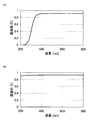
上記構成において、基板は、レーザビームの一部が透過する基板を用いるのが望ましい。しかし、同じ基板でも波長によって透過率が異なる。例として、図2に、波長に対するコーニング社製1737基板および旭硝子社製合成石英ガラス基板の透過率を示す。図2から、波長によって透過率が変化していることが分かる。また、本明細書中では、基板の表面とは膜が形成されている面と定義し、基板の裏面とは膜が形成されている面と反対側の面と定義する。
【0012】
また、上記構成において、金属元素はFe、Co、Ni、Ru、Rh、Pd、Os、Ir、Pt、Cu、Ag、Au、Al、In、Sn、Pb、P、As、Sbから選ばれた一種または複数の元素を用いればよく、前記金属元素を用いた結晶化方法についての詳細は特開平7−183540号公報に記載されている。ここで、前記公報の内容を簡単に説明する。まず、非晶質半導体膜にニッケル、またはパラジウム、または鉛等の金属元素を微量に添加する。添加の方法は、プラズマ処理法や蒸着法、イオン注入法、スパッタ法、溶液塗布法等を利用すればよい。前記添加の後、熱処理を行なうと、結晶性の良好な結晶質半導体膜が得られる。結晶化に最適な加熱温度や加熱時間等は、前記金属元素の添加量や、非晶質半導体膜の状態による。
【0013】
また、上記構成において、不純物元素はn型を付与する不純物元素またはp型を付与する不純物元素であるとする。
【0014】
また、上記構成において、前記レーザビームはパルス発振又は連続発振の気体レーザや固体レーザから発振されたレーザビームを用いることができる。例えば、気体レーザとして、エキシマレーザ、Arレーザ、Krレーザ等があり、固体レーザとして、YAGレーザ、YVO4レーザ、YLFレーザ、YAlO3レーザ、ガラスレーザ、ルビーレーザ、アレキサンドライドレーザ、Ti:サファイアレーザ等を用いることが出来る。また、非線形光学素子により変換された高調波を用いても良い。
【0015】
また、上記構成において、レーザビームは基板の表面側、または裏面側、または表面側および裏面側の両側から照射する。ゲート電極の下方に存在するチャネル形成領域は半導体層の中でも特に良好な結晶性が必要とされる。しかし、チャネル形成領域の上方にはゲート電極が存在し、前記ゲート電極がレーザビームに対して透過性がなければ、半導体層に到達しない。そのため、ゲート電極の材質によって、レーザビームを照射する側を基板の表面側、または裏面側、または表面側および裏面側の両側からにする必要がある。もちろん、レーザビームを表面側から照射する場合は、前記レーザビームに対して透過性を有するゲート電極にする必要がある。また、レーザビームを裏面側から照射する場合は、前記レーザビームに対して透過性を有する基板を用いる必要がある。また、レーザビームを表面側および裏面側から照射する場合は、前記レーザビームに対して透過性を有する基板を用い、かつ、前記レーザビームに対して透過性を有するゲート電極にする必要がある。
【0016】
また、上記構成により作製されたTFTを用いて液晶表示装置やEL表示装置に代表される半導体装置装置を作製することを特徴としている。
【0017】
【発明の実施の形態】
本発明の実施の形態について図1の断面図を用いて説明する。
【0018】
図1(A)において基板11には、合成石英ガラス基板、バリウムホウケイ酸ガラスアルミノホウケイ酸ガラスなどの無アルカリガラスと言ったガラス基板を用いても良い。例えば、コーニング社製の7059ガラスや1737ガラスなどを好適に用いることが出来る。ただし、後工程のレーザビームの照射の際に、基板の裏面側、または表面側および裏面側から照射するのであれば、レーザビームの波長に対し、基板11は透過性を有する必要がある。
【0019】
基板11の上に下地絶縁膜12を公知の手段(LPCVD法、プラズマCVD法等)により窒化珪素膜、酸化窒化珪素膜または酸化珪素膜などで形成する。ただし、下地絶縁膜12は、後工程で用いるレーザ発振器の波長に対し、透過性を有する必要がある。
【0020】
次に、半導体膜12をプラズマCVD法やスパッタ法などの公知の手段で10〜200nm(好ましくは30〜100nm)の厚さに形成したのち、所望の形状にパターニングして半導体層13、14を形成する。ここで、半導体層13はnチャネル型TFTを、半導体層14はpチャネル型TFTを作製するものとする。なお、前記半導体膜12としては、非晶質半導体膜や微結晶半導体膜などがあり、非晶質珪素ゲルマニウム膜などの非晶質構造を有する化合物半導体膜を適用しても良い。
【0021】
次いで、半導体層13、14を覆うゲート絶縁膜15を形成する。ゲート絶縁膜15はプラズマCVD法またはスパッタ法を用い、厚さを40〜150nmとして珪素を含む絶縁膜で形成する。
【0022】
次いで、図1(B)に示すように、ゲート絶縁膜15上に膜厚100〜500nmの導電膜16を形成する。導電膜としては、Ta、W、Ti、Mo、Cu、Cr、Ndから選ばれた元素、または前記元素を主成分とする合金材料若しくは化合物材料で形成してもよいし、多結晶珪素膜に代表される半導体膜を用いてもよい。また、AgPdCu合金を用いてもよい。また、可視光に対して透明な酸化物導電膜(代表的にはITO膜)を用いてもよい。
【0023】
次に、フォトリソグラフィ法を用いてレジストからなるマスク(図示せず)を形成し、電極及び配線を形成するためのエッチング処理を行なって、導電層17、18を形成する。
【0024】
次いで、導電層17、18をマスクとして用い、ゲート絶縁膜15を選択的に除去して絶縁層19、20を形成する。(図1(C))
【0025】
そして、第1および第2のドーピング処理を行ない、半導体層に不純物元素を添加する。(図1(C))ドーピング処理はイオンドープ法、若しくはイオン注入法で行なえば良い。イオンドープ法の条件はドーズ量を1×10¹³〜5×10¹⁵/cm2とし、加速電圧を5〜100keVとして行う。この場合、導電層17、18が不純物元素に対するマスクとなり、自己整合的に不純物領域21、22が形成される。まず、n型を付与する不純物元素を添加して、続いて、p型を付与する不純物元素を添加して不純物領域26、27を形成する。ただし、図1(C)および図1(D)に示すように、n型を付与する不純物元素を添加するときには、pチャネル型TFTを形成する半導体層はレジストからなるマスク23で覆い、p型を付与する不純物元素を添加するときには、nチャネル型TFTを形成する半導体層はレジストからなるマスク25で覆う。
【0026】
次に、金属元素の添加を行なって、金属含有層28を形成する。前記金属元素としては、Fe、Co、Ni、Ru、Rh、Pd、Os、Ir、Pt、Cu、Ag、Au、Al、In、Sn、Pb、P、As、Sbから選ばれた一種または複数の元素を用いればよく、添加の方法は、プラズマ処理法や蒸着法、イオン注入法、スパッタ法、溶液塗布法等を利用すればよい。このとき、図3(C)に示すように、部分的にマスクを形成して、加熱処理により、半導体層が結晶化したときに形成される結晶粒界をチャネル形成領域ではなく、ソース領域またはドレイン領域に形成させる方法もある。
【0027】
次いで、図1(E)に示すように、加熱処理により、半導体層の結晶化および不純物元素の活性化を行なう。この加熱処理はファーネスアニール炉を用いる熱アニール法またはラピッドサーマルアニール法(RTA法)で行なう。結晶化は、半導体層に選択的に添加された金属元素を核として結晶成長し、前記金属元素が添加されていないチャネル形成領域にも横方向に結晶成長して結晶化する。
【0028】
図1(F)は基板の裏面側からレーザビームを照射して、半導体層の結晶性を向上させる工程を説明する図である。この場合、ここでは、裏面側からレーザビームを照射する場合を図示しているが、導電層17、18がレーザビームに対し、透過性を有する材料で形成されていれば、基板の表面側、または表面側および裏面側から照射することもできる。また、用いる基板や下地絶縁膜の膜厚等によって最適な条件は異なる。
【0029】
まず、レーザアニール法において用いるレーザ発振器について説明する。例えば、エキシマレーザは大出力で、現状で300Hz程度の高周波パルスを発振出来る。また、パルス発振のエキシマレーザだけでなく、連続発振のエキシマレーザやその他のパルス発振又は連続発振の気体レーザや固体レーザを用いることができる。例えば、気体レーザとして、Arレーザ、Krレーザ等があり、固体レーザとして、YAGレーザ、YVO4レーザ、YLFレーザ、YAlO3レーザ、ガラスレーザ、ルビーレーザ、アレキサンドライドレーザ、Ti:サファイアレーザ等も用いることが出来る。もちろん、非線形素子により変換された高調波を用いてもよい。また、レーザビームの照射は真空中、大気中、窒素雰囲気中などで行なうことが出来る。さらに、レーザビームを照射する際、基板を500度程度まで加熱しても良い。こうすることで半導体膜における熱の流出速度の低下が期待され、結晶粒の粒径を拡大することができる。
【0030】
前述のいずれかのレーザ発振器を用い、また、いずれかの雰囲気中で、レーザビームを照射して、半導体層の結晶化を行なう。
【0031】
レーザビームを照射して形成された前記結晶質半導体膜は、3〜100%の水素を含む雰囲気中で300〜450℃の加熱処理、あるいは、プラズマによって生成された水素を含む雰囲気中で200〜450℃の加熱処理によって、残留する欠陥を減少することができる。
【0032】
また、前記金属元素がチャネル形成領域に残留した半導体層を用いてTFTを作製すると、その電気的特性のオフ電流値は高くなることが知られている。そのため、本出願人は半導体層から金属元素を除去する技術(ゲッタリング技術)を開発し、特開平10−270363号公報に開示している。前記ゲッタリング技術とは、前記金属元素が残留している前記半導体層に15族に属する元素を選択的に導入して加熱処理を行ない、前記15族に属する元素が導入されている領域(ゲッタリング領域)に前記金属元素を捕獲させることで、前記15族に属する元素が導入されていない領域(被ゲッタリング領域)において前記金属元素を除去または低減することができるというものである。
【0033】
本発明においても、レーザビームを照射した後、前記ゲッタリング技術を利用してもよい。つまり、ゲート電極をマスクとして、15族に属する元素を半導体層に選択的に導入し、加熱処理を行なって、チャネル形成領域から金属元素を除去または低減させてもよい。
【0034】
このようにして作製された結晶質半導体層を用いて、TFTを作製することにより、前記TFTの電気的特性を向上させることが出来る。
【0035】
【実施例】
[実施例1]
本発明の実施例について図1の断面図を用いて説明する。
【0036】
図1(A)において基板11には、合成石英ガラス基板、バリウムホウケイ酸ガラスアルミノホウケイ酸ガラスなどの無アルカリガラスと言ったガラス基板を用いても良い。例えば、コーニング社製の7059ガラスや1737ガラスなどを好適に用いることが出来る。本実施例においては、1737ガラス基板を用いた。
【0037】
前記基板11の上に下地絶縁膜12を公知の手段(LPCVD法、プラズマCVD法等)により窒化珪素膜、酸化窒化珪素膜または酸化珪素膜などで形成する。本実施例では膜厚50nmの酸化窒化珪素膜(組成比Si=32%、O=27%、N=24%、H=17%)を形成した。
【0038】
次に、半導体膜12をプラズマCVD法やスパッタ法などの公知の手段で10〜200nm(好ましくは30〜100nm)の厚さに形成した後、所望の形状にパターニングして半導体層13、14を形成する。ここで、半導体層13はnチャネル型TFTを、半導体層14はpチャネル型TFTを作製するものとする。なお、前記半導体膜12としては、非晶質半導体膜や微結晶半導体膜などがあり、非晶質珪素ゲルマニウム膜などの非晶質構造を有する化合物半導体膜を適用しても良い。本実施例では、プラズマCVD法を用い、55nmの非晶質珪素膜を成膜した。
【0039】
次いで、半導体層13、14を覆うゲート絶縁膜15を形成する。ゲート絶縁膜15はプラズマCVD法またはスパッタ法を用い、厚さを40〜150nmとして珪素を含む絶縁膜で形成する。本実施例では、プラズマCVD法により110nmの厚さで酸化窒化珪素膜(組成比Si=32%、O=59%、N=7%、H=2%)で形成した。勿論、ゲート絶縁膜は酸化窒化珪素膜に限定されるものでなく、他の珪素を含む絶縁膜を単層または積層構造として用いても良い。
【0040】
次いで、図1(B)に示すように、ゲート絶縁膜15上に膜厚100〜500nmの導電膜16を形成する。本実施例では、膜厚30nmのTaN膜からなる導電膜を形成した。TaN膜はスパッタ法で形成し、Taのターゲットを用い、窒素を含む雰囲気内でスパッタした。また、導電膜としては、Ta、W、Ti、Mo、Cu、Cr、Ndから選ばれた元素、または前記元素を主成分とする合金材料若しくは化合物材料で形成してもよいし、多結晶珪素膜に代表される半導体膜を用いてもよい。また、AgPdCu合金を用いてもよい。また、可視光に対して透明な酸化物導電膜(代表的にはITO膜)を用いてもよい。
【0041】
次に、フォトリソグラフィ法を用いてレジストからなるマスク(図示せず)を形成し、電極及び配線を形成するためのエッチング処理を行なって、導電層17、18を形成する。
【0042】
次いで、導電層17、18をマスクとして用い、ゲート絶縁膜15を選択的に除去して絶縁層19、20を形成する。(図1(C))
【0043】
そして、第1および第2のドーピング処理を行ない、半導体層に不純物元素を添加する。(図1(C))ドーピング処理はイオンドープ法、若しくはイオン注入法で行えば良い。イオンドープ法の条件はドーズ量を1×10¹³〜5×10¹⁵/cm2とし、加速電圧を5〜100keVとして行う。この場合、導電層17、18が不純物元素に対するマスクとなり、自己整合的に不純物領域21〜24が形成される。本実施例では、第1のドーピング処理として、n型を付与する不純物元素としてリン(P)を添加して、不純物領域21〜24のリン濃度が1×1020〜5×1021/cm3になるようにした。続いて、第2のドーピング処理を行ない、p型を付与する不純物元素としてボロン(B)を添加して、不純物領域26、27のボロン濃度が1×1020〜1×1022/cm3になるようにした。ただし、図1(D)に示すように、第2のドーピング処理においては、nチャネル型TFTを形成する半導体層はレジストからなるマスク25で覆う。
【0044】
次に、金属元素の添加を行なって、金属含有層28を形成する。前記金属元素としては、ニッケル、またはパラジウム、または鉛等の金属元素があり、添加の方法は、プラズマ処理法や蒸着法、イオン注入法、スパッタ法、溶液塗布法等を利用すればよい。本実施例では、ニッケルを含む溶液を半導体層および導電層に保持させた。
【0045】
次いで、図1(E)に示すように、加熱処理により、半導体層の結晶化および不純物元素の活性化を行なう。この加熱処理はファーネスアニール炉を用いる熱アニール法またはラピッドサーマルアニール法(RTA法)で行なう。結晶化は、半導体層に選択的に添加された金属元素を核として結晶成長し、前記金属元素が添加されていないチャネル形成領域にも横方向に結晶成長して結晶化する。本実施例では、温度550度で4時間の加熱処理を行なった。
【0046】
図1(F)はレーザビームを照射して、半導体層の結晶性を向上させる工程を説明する図である。また、用いる基板や下地絶縁膜の膜厚等によって最適な条件は異なる。まず、レーザアニール法において用いるレーザ発振器について説明する。例えば、エキシマレーザは大出力で、現状で300Hz程度の高周波パルスを発振出来る。また、パルス発振のエキシマレーザだけでなく、連続発振のエキシマレーザやその他のパルス発振又は連続発振の気体レーザや固体レーザを用いることができる。例えば、気体レーザとして、Arレーザ、Krレーザ等があり、固体レーザとして、YAGレーザ、YVO4レーザ、YLFレーザ、YAlO3レーザ、ガラスレーザ、ルビーレーザ、アレキサンドライドレーザ、Ti:サファイアレーザ等も用いることが出来る。もちろん、非線形素子により変換された高調波を用いてもよい。また、レーザビームの照射は真空中、大気中、窒素雰囲気中などで行なうことが出来る。さらに、レーザビームを照射する際、基板を500度程度まで加熱しても良い。こうすることで半導体膜における熱の流出速度の低下が期待され、結晶粒の粒径を拡大することが出来る。
【0047】
本実施例では、YAGレーザの第2高調波(波長532nm)を用い、大気中でレーザビームの照射を行なった。また、本実施例では基板として1737ガラス基板を用いており、図2(B)より、YAGレーザの第2高調波に対する透過率は90%以上ある。そのため、YAGレーザの第2高調波は充分基板を透過する。また、本実施例では、導電層17、18にTaNを用いており、YAGレーザの第2高調波に対して透過性を有しない。そこで本実施例では、基板の裏面側からレーザビームを照射し、前記半導体膜の結晶化を行なった。
【0048】
レーザビームを照射して形成された前記結晶質半導体層は、3〜100%の水素を含む雰囲気中で300〜450℃の加熱処理、あるいは、プラズマによって生成された水素を含む雰囲気中で200〜450℃の加熱処理によって、残留する欠陥を減少することができる。
【0049】
このようにして作製された結晶質半導体層を用いてTFTを作製することにより、前記TFTの電気的特性を向上させることが出来る。
【0050】
[実施例2]
本実施例ではアクティブマトリクス基板の作製方法について図4〜図5を用いて説明する。
【0051】
図1(A)において基板300には、合成石英ガラス基板、バリウムホウケイ酸ガラスアルミノホウケイ酸ガラスなどの無アルカリガラスと言ったガラス基板を用いても良い。例えば、コーニング社製の7059ガラスや1737ガラスなどを好適に用いることが出来る。本実施例においては、1737ガラス基板を用いた。
【0052】
次いで、基板300上に酸化珪素膜、窒化珪素膜または酸化窒化珪素膜などの絶縁膜から成る下地膜301を形成する。本実施例では下地膜301として2層構造を用いるが、前記絶縁膜の単層膜または2層以上積層させた構造を用いても良い。下地膜301の一層目としては、プラズマCVD法を用い、SiH4、NH3、及びN2Oを反応ガスとして成膜される酸化窒化珪素膜301aを10〜200nm(好ましくは50〜100nm)形成する。本実施例では、膜厚50nmの酸化窒化珪素膜301a(組成比Si=32%、O=27%、N=24%、H=17%)を形成した。次いで、下地膜301のニ層目としては、プラズマCVD法を用い、SiH4、及びN2Oを反応ガスとして成膜される酸化窒化珪素膜301bを50〜200nm(好ましくは100〜150nm)の厚さに積層形成する。本実施例では、膜厚100nmの酸化窒化珪素膜401b(組成比Si=32%、O=59%、N=7%、H=2%)を形成した。
【0053】
次いで、下地膜上に半導体膜302を公知の手段(スパッタ法、LPCVD法、またはプラズマCVD法等)により10〜200nm(好ましくは30〜100nm)の厚さに成膜した後、所望の形状にパターニングして半導体層402〜406を形成する。半導体膜の材料に限定はないが、好ましくは珪素または珪素ゲルマニウム(SiGe)合金などで形成すると良い。本実施例では、プラズマCVD法を用い、55nmの非晶質珪素膜を成膜した後、フォトリソグラフィ法を用いたパターニング処理によって、半導体層402〜406を形成した。
【0054】
また、半導体層402〜406を形成した後、TFTのしきい値を制御するために微量な不純物元素(ボロンまたはリン)のドーピングを行なってもよい。
【0055】
次いで、半導体層402〜406を覆うゲート絶縁膜407を形成する。ゲート絶縁膜407はプラズマCVD法またはスパッタ法を用い、厚さを40〜150nmとして珪素を含む絶縁膜で形成する。本実施例では、プラズマCVD法により110nmの厚さで酸化窒化珪素膜(組成比Si=32%、O=59%、N=7%、H=2%)で形成した。もちろん、ゲート絶縁膜は酸化窒化珪素膜に限定されるものでなく、他の珪素を含む絶縁膜を単層または積層構造として用いても良い。
【0056】
また、酸化珪素膜を用いる場合には、プラズマCVD法でTEOS(Tetraethyl Orthosilicate)とO2とを混合し、反応圧力40Pa、基板温度300〜400℃とし、高周波(13.56MHz)電力密度0.5〜0.8W/cm2で放電させて形成することができる。このようにして作製される酸化珪素膜は、その後400〜500℃の熱アニールによりゲート絶縁膜として良好な特性を得ることができる。
【0057】
次いで、図4(B)に示すように、ゲート絶縁膜407上に膜厚20〜100nmの第1の導電膜408と、膜厚100〜400nmの第2の導電膜409とを積層形成する。本実施例では、膜厚30nmのTaN膜からなる第1の導電膜408と、膜厚370nmのW膜からなる第2の導電膜409を積層形成した。TaN膜はスパッタ法で形成し、Taのターゲットを用い、窒素を含む雰囲気内でスパッタした。また、W膜は、Wのターゲットを用いたスパッタ法で形成した。その他に6フッ化タングステン(WF6)を用いる熱CVD法で形成することもできる。いずれにしてもゲート電極として使用するためには低抵抗化を図る必要があり、W膜の抵抗率は20μΩcm以下にすることが望ましい。W膜は結晶粒を大きくすることで低抵抗率化を図ることができるが、W膜中に酸素などの不純物元素が多い場合には結晶化が阻害され高抵抗化する。従って、本実施例では、高純度のW(純度99.9999%)のターゲットを用いたスパッタ法で、さらに成膜時に気相中からの不純物の混入がないように十分配慮してW膜を形成することにより、抵抗率9〜20μΩcmを実現することができた。
【0058】
なお、本実施例では、第1の導電膜408をTaN、第2の導電膜409をWとしたが、特に限定されず、いずれもTa、W、Ti、Mo、Cu、Cr、Ndから選ばれた元素、または前記元素を主成分とする合金材料若しくは化合物材料で形成してもよい。また、リン等の不純物元素をドーピングした多結晶珪素膜に代表される半導体膜を用いてもよい。また、AgPdCu合金を用いてもよい。また、第1の導電膜をタンタル(Ta)膜で形成し、第2の導電膜をW膜とする組み合わせ、第1の導電膜を窒化チタン(TiN)膜で形成し、第2の導電膜をW膜とする組み合わせ、第1の導電膜を窒化タンタル(TaN)膜で形成し、第2の導電膜をAl膜とする組み合わせ、第1の導電膜を窒化タンタル(TaN)膜で形成し、第2の導電膜をCu膜とする組み合わせとしてもよい。
【0059】
次に、フォトリソグラフィ法を用いてレジストからなるマスク410〜415を形成し、電極及び配線を形成するための第1のエッチング処理を行なう。第1のエッチング処理では第1及び第2のエッチング条件で行なう。本実施例では第1のエッチング条件として、ICP(Inductively Coupled Plasma:誘導結合型プラズマ)エッチング法を用い、エッチング用ガスにCF4とCl2とO2とを用い、それぞれのガス流量比を25:25:10(sccm)とし、1Paの圧力でコイル型の電極に500WのRF(13.56MHz)電力を投入してプラズマを生成してエッチングを行った。ここでは、松下電器産業(株)製のICPを用いたドライエッチング装置(Model E645−□ICP)を用いた。基板側(試料ステージ)にも150WのRF(13.56MHz)電力を投入し、実質的に負の自己バイアス電圧を印加する。この第1のエッチング条件によりW膜をエッチングして第1の導電層の端部をテーパー形状とする。
【0060】
この後、レジストからなるマスク410〜415を除去せずに第2のエッチング条件に変え、エッチング用ガスにCF4とCl2とを用い、それぞれのガス流量比を30:30(sccm)とし、1Paの圧力でコイル型の電極に500WのRF(13.56MHz)電力を投入してプラズマを生成して約30秒程度のエッチングを行った。基板側(試料ステージ)にも20WのRF(13.56MHz)電力を投入し、実質的に負の自己バイアス電圧を印加する。CF4とCl2を混合した第2のエッチング条件ではW膜及びTaN膜とも同程度にエッチングされる。なお、ゲート絶縁膜上に残渣を残すことなくエッチングするためには、10〜20%程度の割合でエッチング時間を増加させると良い。
【0061】
上記第1のエッチング処理では、レジストからなるマスクの形状を適したものとすることにより、基板側に印加するバイアス電圧の効果により第1の導電層及び第2の導電層の端部がテーパー形状となる。このテーパー部の角度は15〜45°となる。こうして、第1のエッチング処理により第1の導電層と第2の導電層から成る第1の形状の導電層417〜422(第1の導電層417a〜422aと第2の導電層417b〜422b)を形成する。416はゲート絶縁膜であり、第1の形状の導電層417〜422で覆われない領域は20〜50nm程度エッチングされ薄くなった領域が形成される。
【0062】
そして、レジストからなるマスクを除去せずに第1のドーピング処理を行ない、半導体層にn型を付与する不純物元素を添加する。(図5(A))ドーピング処理はイオンドープ法、若しくはイオン注入法で行なえば良い。イオンドープ法の条件はドーズ量を1×10¹³〜5×10¹⁵atoms/cm2とし、加速電圧を60〜100keVとして行なう。本実施例ではドーズ量を1.5×1015/cm2とし、加速電圧を80keVとして行った。n型を付与する不純物元素として15族に属する元素、典型的にはリン(P)または砒素(As)を用いるが、ここではリン(P)を用いた。この場合、導電層417〜421がn型を付与する不純物元素に対するマスクとなり、自己整合的に第1の高濃度不純物領域306〜310が形成される。第1の高濃度不純物領域306〜310には1×1020〜1×1021atoms/cm3の濃度範囲でn型を付与する不純物元素を添加する。
【0063】
次いで、レジストからなるマスクを除去せずに第2のエッチング処理を行なう。ここでは、エッチングガスにCF4とCl2とO2とを用い、W膜を選択的にエッチングする。この時、第2のエッチング処理により第2の導電層428b〜433bを形成する。一方、第1の導電層417a〜422aは、ほとんどエッチングされず、第2の形状の導電層428〜433を形成する。
【0064】
次いで、レジストからなるマスクを除去せずに、図5(C)に示すように、第2のドーピング処理を行なう。この場合、第1のドーピング処理よりもドーズ量を下げて、70〜120keVの高い加速電圧で、n型を付与する不純物元素を導入する。本実施例ではドーズ量を1.5×10¹⁴/cm2とし、加速電圧を90keVとして行ない、図5(B)で形成された第1の高濃度不純物領域306〜310より内側の半導体層に新たな不純物領域を形成する。第2のドーピング処理は第2の形状の導電層428〜433をマスクとして用い、第2の導電層428b〜433bの下方における半導体層にも不純物元素が導入され、新たに第2の高濃度不純物領域423a〜427aおよび低濃度不純物領域423b〜427bが形成される。
【0065】
次いで、レジストからなるマスクを除去した後、新たにレジストからなるマスク434aおよび434bを形成して、図6(A)に示すように、第3のエッチング処理を行なう。エッチング用ガスにSF6およびCl2とを用い、ガス流量比を50/10(sccm)とし、1.3Paの圧力でコイル型の電極に500WのRF(13.56MHz)電力を投入してプラズマを生成し、約30秒のエッチング処理を行なう。基板側(資料ステージ)には10WのRF(13.56MHz)電力を投入し、実質的には不の自己バイアス電圧を印加する。こうして、前記大3のエッチング処理により、pチャネル型TFTおよび画素部のTFT(画素TFT)のTaN膜をエッチングして、第3の形状の導電層435〜438を形成する。
【0066】
次いで、レジストからなるマスクを除去した後、第2の形状の導電層428、430および第2の形状の導電層435〜438をマスクとして用い、ゲート絶縁膜416を選択的に除去して絶縁層439〜444を形成する。(図6(B))
【0067】
次いで、新たにレジストからなるマスク445a〜445cを形成して第3のドーピング処理を行なう。この第3のドーピング処理により、pチャネル型TFTの活性層となる半導体層に前記一導電型とは逆の導電型を付与する不純物元素が添加された不純物領域446、447を形成する。第2の導電層435a、438aを不純物元素に対するマスクとして用い、p型を付与する不純物元素を添加して自己整合的に不純物領域を形成する。本実施例では、不純物領域446、447はジボラン(B2H6)を用いたイオンドープ法で形成する。(図6(C))この第3のドーピング処理の際には、nチャネル型TFTを形成する半導体層はレジストからなるマスク445a〜445cで覆われている。第1のドーピング処理及び第2のドーピング処理によって、不純物領域446、447にはそれぞれ異なる濃度でリンが添加されているが、そのいずれの領域においてもp型を付与する不純物元素の濃度を2×10²⁰〜2×10²¹atoms/cm3となるようにドーピング処理することにより、pチャネル型TFTのソース領域およびドレイン領域として機能するために何ら問題は生じない。本実施例では、pチャネル型TFTの活性層となる半導体層の一部が露呈しているため、不純物元素(ボロン)を添加しやすい利点を有している。
【0068】
以上までの工程で、それぞれの半導体層に不純物領域が形成される。
【0069】
次いで、レジストからなるマスク445a〜445cを除去して金属元素の添加を行なって、金属含有層361を形成する。前記金属元素としては、ニッケル、またはパラジウム、または鉛等の金属元素があり、添加の方法は、プラズマ処理法や蒸着法、イオン注入法、スパッタ法、溶液塗布法等を利用すればよい。本実施例では、ニッケルを含む溶液を半導体層および導電層に保持させた。
【0070】
次いで、図7(A)に示すように、加熱処理により、半導体層の結晶化および不純物元素の活性化を行なう。この活性化工程はファーネスアニール炉を用いる熱アニール法またはラピッドサーマルアニール法(RTA法)で行なう。熱アニール法としては、酸素濃度が1ppm以下、好ましくは0.1ppm以下の窒素雰囲気中で400〜700℃、代表的には500〜550℃で行えばよく、本実施例では550℃、4時間の熱処理で活性化処理を行った。
【0071】
図7(B)はレーザビームを照射して、半導体層の結晶性を向上させる工程を説明する図である。用いる基板や下地絶縁膜の膜厚等によって最適な条件は異なる。まず、レーザアニール法において用いるレーザ発振器について説明する。例えば、エキシマレーザは大出力で、現状で300Hz程度の高周波パルスを発振出来る。また、パルス発振のエキシマレーザだけでなく、連続発振のエキシマレーザやその他のパルス発振又は連続発振の気体レーザや固体レーザを用いることができる。例えば、気体レーザとして、Arレーザ、Krレーザ等があり、固体レーザとして、YAGレーザ、YVO4レーザ、YLFレーザ、YAlO3レーザ、ガラスレーザ、ルビーレーザ、アレキサンドライドレーザ、Ti:サファイアレーザ等も用いることが出来る。もちろん、非線形素子により変換された高調波を用いてもよい。また、レーザビームの照射は真空中、大気中、窒素雰囲気中などで行なうことが出来る。さらに、レーザビームを照射する際、基板を500度程度まで加熱しても良い。こうすることで半導体膜における熱の流出速度の低下が期待され、結晶粒の粒径を拡大することが出来る。
【0072】
本実施例では、YAGレーザの第2高調波(波長532nm)を用い、大気中でレーザビームの照射を行なった。また、本実施例では基板として1737ガラス基板を用いており、図2(B)より、YAGレーザの第2高調波に対する透過率は90%以上ある。そのため、YAGレーザの第2高調波は充分基板を透過する。また、本実施例では、導電層428、430、435、436、437、438にTaNおよびWを用いており、YAGレーザの第2高調波に対して透過性を有しない。そこで本実施例では、基板の裏面側からレーザビームを照射し、前記半導体膜の結晶化を行なった。
【0073】
次いで、第1の層間絶縁膜461を形成する。この第1の層間絶縁膜461としては、プラズマCVD法またはスパッタ法を用い、厚さを100〜200nmとして珪素を含む絶縁膜で形成する。本実施例では、プラズマCVD法により膜厚150nmの酸化窒化珪素膜を形成した。もちろん、第1の層間絶縁膜461は酸化窒化珪素膜に限定されるものでなく、他の珪素を含む絶縁膜を単層または積層構造として用いても良い。
【0074】
そして、3〜100%の水素を含む雰囲気中で、300〜550℃で1〜12時間の熱処理を行ない、半導体層を水素化する工程を行なう。本実施例では水素を約3%の含む窒素雰囲気中で410℃、1時間の熱処理を行った。この工程は層間絶縁膜に含まれる水素により半導体層のダングリングボンドを終端する工程である。水素化の他の手段として、プラズマ水素化(プラズマにより励起された水素を用いる)を行なっても良い。
【0075】
次いで、第1の層間絶縁膜461上に無機絶縁膜材料または有機絶縁物材料から成る第2の層間絶縁膜462を形成する。本実施例では、膜厚1.6μmのアクリル樹脂膜を形成したが、粘度が10〜1000cp、好ましくは40〜200cpのものを用い、表面に凸凹が形成されるものを用いた。
【0076】
本実施例では、鏡面反射を防ぐため、表面に凸凹が形成される第2の層間絶縁膜を形成することによって画素電極の表面に凸凹を形成した。また、画素電極の表面に凹凸を持たせて光散乱性を図るため、画素電極の下方の領域に凸部を形成してもよい。その場合、凸部の形成は、TFTの形成と同じフォトマスクで行なうことができるため、工程数の増加なく形成することができる。なお、この凸部は配線及びTFT部以外の画素部領域の基板上に適宜設ければよい。こうして、凸部を覆う絶縁膜の表面に形成された凸凹に沿って画素電極の表面に凸凹が形成される。
【0077】
また、第2の層間絶縁膜462として表面が平坦化する膜を用いてもよい。その場合は、画素電極を形成した後、公知のサンドブラスト法やエッチング法等の工程を追加して表面を凹凸化させて、鏡面反射を防ぎ、反射光を散乱させることによって白色度を増加させることが好ましい。
【0078】
そして、駆動回路506において、各不純物領域とそれぞれ電気的に接続する配線463〜467を形成する。なお、これらの配線は、膜厚50nmのTi膜と、膜厚500nmの合金膜(AlとTiとの合金膜)との積層膜をパターニングして形成する。
【0079】
また、画素部507においては、画素電極470、ゲート配線469、接続電極468を形成する。(図7(B))この接続電極468によりソース配線(443bと449の積層)は、画素TFTと電気的な接続が形成される。また、ゲート配線469は、画素TFTのゲート電極と電気的な接続が形成される。また、画素電極470は、画素TFTのドレイン領域442と電気的な接続が形成され、さらに保持容量を形成する一方の電極として機能する半導体層458と電気的な接続が形成される。また、画素電極471としては、AlまたはAgを主成分とする膜、またはそれらの積層膜等の反射性の優れた材料を用いることが望ましい。
【0080】
以上の様にして、nチャネル型TFT501とpチャネル型TFT502からなるCMOS回路、及びnチャネル型TFT503を有する駆動回路506と、画素TFT504、保持容量505とを有する画素部507を同一基板上に形成することができる。こうして、アクティブマトリクス基板が完成する。
【0081】
駆動回路506のnチャネル型TFT501はチャネル形成領域423c、ゲート電極の一部を構成する第1の導電層428aと重なる低濃度不純物領域423b(GOLD領域)、とソース領域またはドレイン領域として機能する高濃度不純物領域423aを有している。このnチャネル型TFT501と電極466で接続してCMOS回路を形成するpチャネル型TFT502にはチャネル形成領域446d、ゲート電極の外側に形成される不純物領域446b、446c、ソース領域またはドレイン領域として機能する高濃度不純物領域446aを有している。また、nチャネル型TFT503にはチャネル形成領域425c、ゲート電極の一部を構成する第1の導電層430aと重なる低濃度不純物領域425b(GOLD領域)、とソース領域またはドレイン領域として機能する高濃度不純物領域425aを有している。
【0082】
画素部の画素TFT504にはチャネル形成領域426c、ゲート電極の外側に形成される低濃度不純物領域426b(LDD領域)とソース領域またはドレイン領域として機能する高濃度不純物領域426aを有している。また、保持容量505の一方の電極として機能する半導体層447a、447bには、それぞれp型を付与する不純物元素が添加されている。保持容量505は、絶縁膜444を誘電体として、電極(438aと438bの積層)と、半導体層447a〜447cとで形成している。
【0083】
また、本実施例の画素構造は、ブラックマトリクスを用いることなく、画素電極間の隙間が遮光されるように、画素電極の端部をソース配線と重なるように配置形成する。
【0084】
また、本実施例で作製するアクティブマトリクス基板の画素部の上面図を図8に示す。なお、図4〜図7に対応する部分には同じ符号を用いている。図7中の鎖線A−A’は図8中の鎖線A―A’で切断した断面図に対応している。また、図7中の鎖線B−B’は図8中の鎖線B―B’で切断した断面図に対応している。
【0085】
[実施例3]
本実施例では、実施例2で作製したアクティブマトリクス基板から、反射型液晶表示装置を作製する工程を以下に説明する。説明には図9を用いる。
【0086】
まず、実施例2に従い、図7の状態のアクティブマトリクス基板を得た後、図7のアクティブマトリクス基板上、少なくとも画素電極470上に配向膜471を形成しラビング処理を行う。なお、本実施例では配向膜471を形成する前に、アクリル樹脂膜等の有機樹脂膜をパターニングすることによって基板間隔を保持するための柱状のスペーサ(図示しない)を所望の位置に形成した。また、柱状のスペーサに代えて、球状のスペーサを基板全面に散布してもよい。
【0087】
次いで、対向基板471を用意する。次いで、対向基板471上に着色層472、473、平坦化膜474を形成する。赤色の着色層472と青色の着色層473とを重ねて、遮光部を形成する。また、赤色の着色層と緑色の着色層とを一部重ねて、遮光部を形成してもよい。
【0088】
本実施例では、実施例2に示す基板を用いている。従って、実施例2の画素部の上面図を示す図8では、少なくともゲート配線469と画素電極470の間隙と、ゲート配線469と接続電極468の間隙と、接続電極468と画素電極470の間隙を遮光する必要がある。本実施例では、それらの遮光すべき位置に着色層の積層からなる遮光部が重なるように各着色層を配置して、対向基板を貼り合わせた。
【0089】
このように、ブラックマスク等の遮光層を形成することなく、各画素間の隙間を着色層の積層からなる遮光部で遮光することによって工程数の低減を可能とした。
【0090】
次いで、平坦化膜474上に透明導電膜からなる対向電極475を少なくとも画素部に形成し、対向基板の全面に配向膜476を形成し、ラビング処理を施した。
【0091】
そして、画素部と駆動回路が形成されたアクティブマトリクス基板と対向基板とをシール材477で貼り合わせる。シール材477にはフィラーが混入されていて、このフィラーと柱状スペーサによって均一な間隔を持って2枚の基板が貼り合わせられる。その後、両基板の間に液晶材料478を注入し、封止剤(図示せず)によって完全に封止する。液晶材料478には公知の液晶材料を用いれば良い。このようにして図9に示す反射型液晶表示装置が完成する。そして、必要があれば、アクティブマトリクス基板または対向基板を所望の形状に分断する。さらに、対向基板のみに偏光板(図示しない)を貼りつけた。そして、公知の技術を用いてFPCを貼りつけた。
【0092】
以上のようにして作製される液晶表示パネルは各種電子機器の表示部として用いることができる。
【0093】
なお、本実施例は実施例1または実施例2と自由に組み合わせることが可能である。
【0094】
[実施例4]
本実施例では、実施例2で示したアクティブマトリクス基板を作製するときのTFTの作製方法を用いて、EL(エレクトロルミネセンス)表示装置を作製した例について説明する。なお、図10は本発明のEL表示装置の断面図である。
【0095】
本明細書において、EL表示装置とは、基板上に形成された発光素子を該基板とカバー材の間に封入した表示用パネルおよび該表示用パネルにTFTを実装した表示用モジュールを総称したものである。なお、発光素子は、電場を加えることで発生するルミネッセンス(Electro Luminescence)が得られる有機化合物を含む層(発光層)と陽極層と、陰極層とを有する。また、有機化合物におけるルミネッセンスには、一重項励起状態から基底状態に戻る際の発光(蛍光)と三重項励起状態から基底状態に戻る際の発光(リン光)があり、これらのうちどちらか、あるいは両方の発光を含む。
【0096】
図10において、基板700上に設けられたスイッチングTFT603は図10のnチャネル型TFT503を用いて形成される。したがって、構造の説明はnチャネル型TFT503の説明を参照すれば良い。
【0097】
なお、本実施例ではチャネル形成領域が二つ形成されるダブルゲート構造としているが、チャネル形成領域が一つ形成されるシングルゲート構造もしくは三つ形成されるトリプルゲート構造であっても良い。
【0098】
基板700上に設けられた駆動回路は図10のCMOS回路を用いて形成される。従って、構造の説明はnチャネル型TFT501とpチャネル型TFT502の説明を参照すれば良い。なお、本実施例ではシングルゲート構造としているが、ダブルゲート構造もしくはトリプルゲート構造であっても良い。
【0099】
また、配線701、703はCMOS回路のソース配線、702はドレイン配線として機能する。また、配線704はソース配線708とスイッチングTFTのソース領域とを電気的に接続する配線として機能し、配線705はドレイン配線709とスイッチングTFTのドレイン領域とを電気的に接続する配線として機能する。
【0100】
なお、電流制御TFT604は図10のpチャネル型TFT502を用いて形成される。従って、構造の説明はpチャネル型TFT502の説明を参照すれば良い。なお、本実施例ではシングルゲート構造としているが、ダブルゲート構造もしくはトリプルゲート構造であっても良い。
【0101】
また、配線706は電流制御TFTのソース配線(電流供給線に相当する)であり、707は電流制御TFTの画素電極710上に重ねることで画素電極710と電気的に接続する電極である。
【0102】
なお、710は、透明導電膜からなる画素電極(EL素子の陽極)である。透明導電膜としては、酸化インジウムと酸化スズとの化合物、酸化インジウムと酸化亜鉛との化合物、酸化亜鉛、酸化スズまたは酸化インジウムを用いることができる。また、前記透明導電膜にガリウムを添加したものを用いても良い。画素電極710は、上記配線を形成する前に平坦な層間絶縁膜711上に形成する。本実施例においては、樹脂からなる平坦化膜711を用いてTFTによる段差を平坦化することは非常に重要である。後に形成されるEL層は非常に薄いため、段差が存在することによって発光不良を起こす場合がある。従って、EL層をできるだけ平坦面に形成しうるように画素電極を形成する前に平坦化しておくことが望ましい。
【0103】
配線701〜707を形成後、図10に示すようにバンク712を形成する。バンク712は100〜400nmの珪素を含む絶縁膜もしくは有機樹脂膜をパターニングして形成すれば良い。
【0104】
なお、バンク712は絶縁膜であるため、成膜時における素子の静電破壊には注意が必要である。本実施例ではバンク712の材料となる絶縁膜中にカーボン粒子や金属粒子を添加して抵抗率を下げ、静電気の発生を抑制する。この際、抵抗率は1×10⁶〜1×10¹²Ωm(好ましくは1×10⁸〜1×10¹⁰Ωm)となるようにカーボン粒子や金属粒子の添加量を調節すれば良い。
【0105】
画素電極710の上にはEL層713が形成される。なお、図10では一画素しか図示していないが、本実施例ではR(赤)、G(緑)、B(青)の各色に対応したEL層を作り分けている。また、本実施例では蒸着法により低分子系有機EL材料を形成している。具体的には、正孔注入層として20nm厚の銅フタロシアニン(CuPc)膜を設け、その上に発光層として70nm厚のトリス−8−キノリノラトアルミニウム錯体(Alq3)膜を設けた積層構造としている。Alq3にキナクリドン、ペリレンもしくはDCM1といった蛍光色素を添加することで発光色を制御することができる。
【0106】
但し、以上の例はEL層として用いることのできる有機EL材料の一例であって、これに限定する必要はまったくない。発光層、電荷輸送層または電荷注入層を自由に組み合わせてEL層(発光及びそのためのキャリアの移動を行なわせるための層)を形成すれば良い。例えば、本実施例では低分子系有機EL材料をEL層として用いる例を示したが、高分子系有機EL材料を用いても良い。また、電荷輸送層や電荷注入層として炭化珪素等の無機材料を用いることも可能である。これらの有機EL材料や無機材料は公知の材料を用いることができる。
但し、以上の例はEL層として用いることのできる有機EL材料の一例であって、これに限定する必要はまったくない。発光層、電荷輸送層または電荷注入層を自由に組み合わせてEL層(発光及びそのためのキャリアの移動を行わせるための層)を形成すれば良い。例えば、本実施例では低分子系有機EL材料をEL層として用いる例を示したが、中分子系有機EL材料や高分子系有機EL材料を用いても良い。なお、本明細書中において、昇華性を有さず、かつ、分子数が20以下または連鎖する分子の長さが10μm以下の有機EL材料を中分子系有機EL材料とする。また、高分子系有機EL材料を用いる例として、正孔注入層として20nmのポリチオフェン(PEDOT)膜をスピン塗布法により設け、その上にEL層として100nm程度のパラフェニレンビニレン(PPV)膜を設けた積層構造としても良い。なお、PPVのπ共役系高分子を用いると、赤色から青色まで発光波長を選択できる。また、電荷輸送層や電荷注入層として炭化珪素等の無機材料を用いることも可能である。これらの有機EL材料や無機材料は公知の材料を用いることができる。
【0107】
次に、EL層713の上には導電膜からなる陰極714が設けられる。本実施例の場合、導電膜としてアルミニウムとリチウムとの合金膜を用いる。勿論、公知のMgAg膜(マグネシウムと銀との合金膜)を用いても良い。陰極材料としては、周期表の1族もしくは2族に属する元素からなる導電膜もしくはそれらの元素を添加した導電膜を用いれば良い。
【0108】
この陰極714まで形成された時点でEL素子715が完成する。なお、ここでいうEL素子715は、画素電極(陽極)710、EL層713及び陰極714で形成されたコンデンサを指す。
【0109】
EL素子715を完全に覆うようにしてパッシベーション膜716を設けることは有効である。パッシベーション膜716としては、炭素膜、窒化珪素膜もしくは窒化酸化珪素膜を含む絶縁膜からなり、該絶縁膜を単層もしくは組み合わせた積層で用いる。
【0110】
この際、カバレッジの良い膜をパッシベーション膜として用いることが好ましく、炭素膜、特にDLC(ダイヤモンドライクカーボン)膜を用いることは有効である。DLC膜は室温から100℃以下の温度範囲で成膜可能であるため、耐熱性の低いEL層713の上方にも容易に成膜することができる。また、DLC膜は酸素に対するブロッキング効果が高く、EL層713の酸化を抑制することが可能である。そのため、この後に続く封止工程を行う間にEL層713が酸化するといった問題を防止できる。
【0111】
さらに、パッシベーション膜716上に封止材717を設け、カバー材718を貼り合わせる。封止材717としては紫外線硬化樹脂を用いれば良く、内部に吸湿効果を有する物質もしくは酸化防止効果を有する物質を設けることは有効である。また、本実施例においてカバー材718はガラス基板や石英基板やプラスチック基板(プラスチックフィルムも含む)の両面に炭素膜(好ましくはダイヤモンドライクカーボン膜)を形成したものを用いる。
【0112】
こうして図10に示すような構造のEL表示装置が完成する。なお、バンク712を形成した後、パッシベーション膜716を形成するまでの工程をマルチチャンバー方式(またはインライン方式)の成膜装置を用いて、大気解放せずに連続的に処理することは有効である。また、さらに発展させてカバー材718を貼り合わせる工程までを大気解放せずに連続的に処理することも可能である。
【0113】
こうして、プラスチック基板を母体とする絶縁体501上にnチャネル型TFT601、602、スイッチングTFT(nチャネル型TFT)603および電流制御TFT(nチャネル型TFT)604が形成される。ここまでの製造工程で必要としたマスク数は、一般的なアクティブマトリクス型EL表示装置よりも少ない。
【0114】
即ち、TFTの製造工程が大幅に簡略化されており、歩留まりの向上および製造コストの低減が実現できる。
【0115】
さらに、図10を用いて説明したように、ゲート電極に絶縁膜を介して重なる不純物領域を設けることによりホットキャリア効果に起因する劣化に強いnチャネル型TFTを形成することができる。そのため、信頼性の高いEL表示装置を実現できる。
【0116】
また、本実施例では画素部と駆動回路の構成のみ示しているが、本実施例の製造工程に従えば、その他にも信号分割回路、D/Aコンバータ、オペアンプ、γ補正回路などの論理回路を同一の絶縁体上に形成可能であり、さらにはメモリやマイクロプロセッサをも形成しうる。
【0117】
さらに、EL素子を保護するための封止(または封入)工程まで行った後の本実施例のEL発光装置について図11を用いて説明する。なお、必要に応じて図10で用いた符号を引用する。
【0118】
図11(A)は、EL素子の封止までを行った状態を示す上面図、図11(B)は図11(A)をC−C’で切断した断面図である。点線で示された801はソース側駆動回路、806は画素部、807はゲート側駆動回路である。また、901はカバー材、902は第1シール材、903は第2シール材であり、第1シール材902で囲まれた内側には封止材907が設けられる。
【0119】
なお、904はソース側駆動回路801及びゲート側駆動回路807に入力される信号を伝送するための配線であり、外部入力端子となるFPC(フレキシブルプリントサーキット)905からビデオ信号やクロック信号を受け取る。なお、ここではFPCしか図示されていないが、このFPCにはプリント配線基盤(PWB)が取り付けられていても良い。本明細書におけるEL表示装置には、EL表示装置本体だけでなく、それにFPCもしくはPWBが取り付けられた状態をも含むものとする。
【0120】
次に、断面構造について図11(B)を用いて説明する。基板700の上方には画素部806、ゲート側駆動回路807が形成されており、画素部806は電流制御TFT604とそのドレインに電気的に接続された画素電極710を含む複数の画素により形成される。また、ゲート側駆動回路807はnチャネル型TFT601とpチャネル型TFT602とを組み合わせたCMOS回路(図14参照)を用いて形成される。
【0121】
画素電極710はEL素子の陽極として機能する。また、画素電極710の両端にはバンク712が形成され、画素電極710上にはEL層713およびEL素子の陰極714が形成される。
【0122】
陰極714は全画素に共通の配線としても機能し、接続配線904を経由してFPC905に電気的に接続されている。さらに、画素部806及びゲート側駆動回路807に含まれる素子は全て陰極714およびパッシベーション膜567で覆われている。
【0123】
また、第1シール材902によりカバー材901が貼り合わされている。なお、カバー材901とEL素子との間隔を確保するために樹脂膜からなるスペーサを設けても良い。そして、第1シール材902の内側には封止材907が充填されている。なお、第1シール材902、封止材907としてはエポキシ系樹脂を用いるのが好ましい。また、第1シール材902はできるだけ水分や酸素を透過しない材料であることが望ましい。さらに、封止材907の内部に吸湿効果をもつ物質や酸化防止効果をもつ物質を含有させても良い。
【0124】
EL素子を覆うようにして設けられた封止材907はカバー材901を接着するための接着剤としても機能する。また、本実施例ではカバー材901を構成するプラスチック基板901aの材料としてFRP(Fiberglass-Reinforced Plastics)、PVF(ポリビニルフロライド)、マイラー、ポリエステルまたはアクリルを用いることができる。
【0125】
また、封止材907を用いてカバー材901を接着した後、封止材907の側面(露呈面)を覆うように第2シール材903を設ける。第2シール材903は第1シール材902と同じ材料を用いることができる。
【0126】
以上のような構造でEL素子を封止材907に封入することにより、EL素子を外部から完全に遮断することができ、外部から水分や酸素等のEL層の酸化による劣化を促す物質が侵入することを防ぐことができる。従って、信頼性の高いEL表示装置が得られる。
【0127】
なお、本実施例は実施例1または実施例2と自由に組み合わせることが可能である。
【0128】
[実施例5]
本発明を実施して形成されたCMOS回路や画素部は様々な半導体装置(アクティブマトリクス型液晶ディスプレイ、アクティブマトリクス型ECディスプレイ、アクティブマトリクス型ELディスプレイ)に用いることが出来る。即ち、それら電気光学装置を表示部に組み込んだ電子機器全てに本発明を実施出来る。
【0129】
その様な電子機器としては、ビデオカメラ、デジタルカメラ、プロジェクター(リア型またはフロント型)、ヘッドマウントディスプレイ(ゴーグル型ディスプレイ)、カーナビゲーション、カーステレオ、パーソナルコンピュータ、携帯情報端末(モバイルコンピュータ、携帯電話または電子書籍等)などが挙げられる。それらの一例を図12、図13及び図14に示す。
【0130】
図12(A)はパーソナルコンピュータであり、本体3001、画像入力部3002、表示部3003、キーボード3004等を含む。本発明を画像入力部3002、表示部3003やその他の信号制御回路に適用することが出来る。
【0131】
図12(B)はビデオカメラであり、本体3101、表示部3102、音声入力部3103、操作スイッチ3104、バッテリー3105、受像部3106等を含む。本発明を表示部3102やその他の信号制御回路に適用することが出来る。
【0132】
図12(C)はモバイルコンピュータ(モービルコンピュータ)であり、本体3201、カメラ部3202、受像部3203、操作スイッチ3204、表示部3205等を含む。本発明は表示部3205やその他の信号制御回路に適用出来る。
【0133】
図12(D)はゴーグル型ディスプレイであり、本体3301、表示部3302、アーム部3303等を含む。本発明は表示部3302やその他の信号制御回路に適用することが出来る。
【0134】
図12(E)はプログラムを記録した記録媒体(以下、記録媒体と呼ぶ)を用いるプレーヤーであり、本体3401、表示部3402、スピーカ部3403、記録媒体3404、操作スイッチ3405等を含む。なお、このプレーヤーは記録媒体としてDVD(Digtial Versatile Disc)、CD等を用い、音楽鑑賞や映画鑑賞やゲームやインターネットを行うことが出来る。本発明は表示部3402やその他の信号制御回路に適用することが出来る。
【0135】
図12(F)はデジタルカメラであり、本体3501、表示部3502、接眼部3503、操作スイッチ3504、受像部(図示しない)等を含む。本発明を表示部3502やその他の信号制御回路に適用することが出来る。
【0136】
図13(A)はフロント型プロジェクターであり、投射装置3601、スクリーン3602等を含む。本発明は投射装置3601の一部を構成する液晶表示装置3808やその他の信号制御回路に適用することが出来る。
【0137】
図13(B)はリア型プロジェクターであり、本体3701、投射装置3702、ミラー3703、スクリーン3704等を含む。本発明は投射装置3702の一部を構成する液晶表示装置3808やその他の信号制御回路に適用することが出来る。
【0138】
なお、図13(C)は、図13(A)及び図13(B)中における投射装置3601、3702の構造の一例を示した図である。投射装置3601、3702は、光源光学系3801、ミラー3802、3804〜3806、ダイクロイックミラー3803、プリズム3807、液晶表示装置3808、位相差板3809、投射光学系3810で構成される。投射光学系3810は、投射レンズを含む光学系で構成される。本実施例は三板式の例を示したが、特に限定されず、例えば単板式であってもよい。また、図13(C)中において矢印で示した光路に実施者が適宜、光学レンズや、偏光機能を有するフィルムや、位相差を調節するためのフィルム、IRフィルム等の光学系を設けてもよい。
【0139】
また、図13(D)は、図13(C)中における光源光学系3801の構造の一例を示した図である。本実施例では、光源光学系3801は、リフレクター3811、光源3812、レンズアレイ3813、3814、偏光変換素子3815、集光レンズ3816で構成される。なお、図13(D)に示した光源光学系は一例であって特に限定されない。例えば、光源光学系に実施者が適宜、光学レンズや、偏光機能を有するフィルムや、位相差を調節するフィルム、IRフィルム等の光学系を設けてもよい。
【0140】
ただし、図13に示したプロジェクターにおいては、透過型の電気光学装置を用いた場合を示しており、反射型の電気光学装置での適用例は図示していない。
【0141】
図14(A)は携帯電話であり、本体3901、音声出力部3902、音声入力部3903、表示部3904、操作スイッチ3905、アンテナ3906等を含む。本発明を音声出力部3902、音声入力部3903、表示部3904やその他の信号制御回路に適用することが出来る。
【0142】
図14(B)は携帯書籍(電子書籍)であり、本体4001、表示部4002、4003、記憶媒体4004、操作スイッチ4005、アンテナ4006等を含む。本発明は表示部4002、4003やその他の信号回路に適用することが出来る。
【0143】
図14(C)はディスプレイであり、本体4101、支持台4102、表示部4103等を含む。本発明は表示部4103に適用することが出来る。本発明のディスプレイは特に大画面化した場合において有利であり、対角10インチ以上(特に30インチ以上)のディスプレイには有利である。
【0144】
以上の様に、本発明の適用範囲は極めて広く、あらゆる分野の電子機器に適用することが可能である。また、本実施例の電子機器は実施例1〜4のどのような組み合わせからなる構成を用いても実現することが出来る
【0145】
【発明の効果】
本発明の構成を採用することにより、以下に示すような基本的有意性を得ることが出来る。
(a)従来のTFTの作製プロセスに適合した、簡単な構造である。
(b)スリットなどの位置決めのために、レーザ照射装置に特別なミクロンオーダーでの精密な位置決め技術は不要であり、通常のレーザ照射装置をそのまま利用できる。
(c)以上の利点を満たした上で、結晶性の良好な半導体層を作製できる方法である。
【図面の簡単な説明】
【図1】 本発明が開示するTFTの作製方法の例を示す図。
【図2】 波長に対する基板の透過率の例を示す図。
【図3】 従来技術の例を示す図。
【図4】 画素TFT、駆動回路のTFTの作製工程を示す断面図。
【図5】 画素TFT、駆動回路のTFTの作製工程を示す断面図。
【図6】 画素TFT、駆動回路のTFTの作製工程を示す断面図。
【図7】 画素TFT、駆動回路のTFTの作製工程を示す断面図。
【図8】 画素TFTの構成を示す上面図。
【図9】 アクティブマトリクス型液晶表示装置の作製工程を示す断面図。
【図10】 EL表示装置の駆動回路及び画素部の断面構造図。
【図11】 (A)EL表示装置の上面図。
(B)EL表示装置の駆動回路及び画素部の断面構造図。
【図12】 半導体装置の例を示す図。
【図13】 半導体装置の例を示す図。
【図14】 半導体装置の例を示す図。[0001]
BACKGROUND OF THE INVENTION
The present invention relates to a method for manufacturing a semiconductor device having a circuit including thin film transistors (hereinafter referred to as TFTs). For example, the present invention relates to an electro-optical device typified by a liquid crystal display device and a configuration of an electric apparatus in which the electro-optical device is mounted as a component. Further, the present invention relates to a method for manufacturing the device. Note that in this specification, a semiconductor device refers to all devices that can function by utilizing semiconductor characteristics, and the electro-optical device and the electric appliance are also included in the category.
[0002]
[Prior art]
In recent years, a thin film transistor (TFT) is formed using a semiconductor thin film (thickness of about several to several hundred nm) formed on a substrate having an insulating surface, and a semiconductor device having a large-area integrated circuit formed using this TFT is developed. Is progressing. Active matrix liquid crystal display devices, EL display devices, and contact image sensors are known as representative examples. In particular, a TFT using a crystalline semiconductor film (typically a crystalline silicon film) as an active region has high field effect mobility, and thus various functional circuits can be formed.
[0003]
The crystallinity of the crystalline semiconductor film has a great influence on the electrical characteristics when a TFT is manufactured. At present, an amorphous semiconductor film is often crystallized to form a crystalline semiconductor film. Crystallinity expresses the degree of regularity of atomic arrangement in a crystal. When a TFT is manufactured using a crystalline semiconductor film having good crystallinity, its electrical characteristics are considered good. Become.
[0004]
Further, as a process that particularly affects the crystallinity of the semiconductor film, a doping process can be given. In the doping process, the energy of ions implanted into the semiconductor film is much larger than the binding energy of the elements forming the semiconductor film. For this reason, ions implanted into the semiconductor film blow off the elements forming the semiconductor film from the lattice points and cause defects in the crystal. Therefore, heat treatment is often performed after the doping treatment in order to recover the defects and activate the implanted ions at the same time.
[0005]
As described above, the crystallinity of the semiconductor film is affected in various ways during the process of manufacturing the TFT, but attempts have been made to manufacture a crystalline semiconductor film with good crystallinity.
[0006]
For example, it is described in “High-Performance Low-Temperature Poly-Silicon Thin Film Transistors Fabricated by New Metal-Induced Lateral Crystallization Process; Jpn. J. Appl. Phys. Vol. 37 (1998) pp. 4244-4247”. A method will be described. After an amorphous silicon layer having a desired shape is formed on the substrate, a gate insulating film and a gate electrode are formed. Next, nickel (Ni) is added, and then an impurity element doping process is performed. Here, since the gate electrode is formed on the semiconductor layer, nickel is added to the source region and the drain region, but not to the channel formation region. Thereafter, the amorphous silicon layer is crystallized and the impurity elements are activated simultaneously by heat treatment. As already described, nickel is not added to the channel formation region. (FIG. 3A) However, since the crystal is grown in the lateral direction using nickel added to the source region and the drain region as a nucleus, the channel formation region is also crystallized. (FIG. 3B) Further, in order to avoid crystal grains grown laterally from the source region and the drain region from colliding with each other in the channel formation region to form a large grain boundary, as shown in FIG. A method of crystallizing after partially providing a mask, adding nickel, removing the mask, has also been reported. (Fig. 3 (D))
[0007]
[Problems to be solved by the invention]
However, good electrical characteristics are not obtained in a TFT manufactured by the above method. In particular, the characteristics of the subthreshold coefficient (S value) and field effect mobility, which are important parameters for judging the performance of the TFT, are not good.
[0008]
The present invention is a technique for solving such problems. In an electro-optical device and a semiconductor device typified by an active matrix liquid crystal display device manufactured using TFTs, the operating characteristics and reliability of the semiconductor device are disclosed. It aims at realizing improvement.
[0009]
[Means for Solving the Problems]
The present invention is characterized in that the crystallinity of the semiconductor layer is further improved by irradiating a laser beam after performing crystallization by heat treatment on the semiconductor layer to which a metal element is selectively added. By the heat treatment, crystal growth is performed in a lateral direction from a region where the metal element is added to a region where the metal element is not added. Therefore, an amorphous region may remain without being crystallized in the semiconductor layer to which the metal element is not added. In addition, the semiconductor layer after the heat treatment has many defects in crystal grains. In view of this, the remaining amorphous region is crystallized and crystal defects are compensated by irradiating a laser beam after the heat treatment.
[0010]
In the half structure of the present invention disclosed in this specification, a semiconductor layer is formed over a substrate, an insulating film is formed over the semiconductor layer, a gate electrode is formed over the insulating film, and the gate electrode is used as a mask. An impurity element is introduced into the semiconductor layer, a metal element is selectively introduced into the semiconductor layer into which the impurity element is introduced, the semiconductor layer is crystallized by heat treatment, the impurity element is activated, and a laser beam It is characterized by irradiating.
[0011]
In the above structure, it is preferable to use a substrate through which a part of the laser beam is transmitted. However, the transmittance varies depending on the wavelength even on the same substrate. As an example, FIG. 2 shows the transmittance of Corning 1737 substrate and Asahi Glass synthetic quartz glass substrate with respect to wavelength. From FIG. 2, it can be seen that the transmittance varies depending on the wavelength. In this specification, the surface of the substrate is defined as a surface on which a film is formed, and the back surface of the substrate is defined as a surface on the opposite side to the surface on which the film is formed.
[0012]
In the above configuration, the metal element is selected from Fe, Co, Ni, Ru, Rh, Pd, Os, Ir, Pt, Cu, Ag, Au, Al, In, Sn, Pb, P, As, and Sb. One or more elements may be used, and details of the crystallization method using the metal element are described in JP-A-7-183540. Here, the contents of the publication will be briefly described. First, a trace amount of a metal element such as nickel, palladium, or lead is added to the amorphous semiconductor film. As the addition method, a plasma treatment method, a vapor deposition method, an ion implantation method, a sputtering method, a solution coating method, or the like may be used. When heat treatment is performed after the addition, a crystalline semiconductor film with good crystallinity can be obtained. The optimal heating temperature, heating time, etc. for crystallization depend on the amount of the metal element added and the state of the amorphous semiconductor film.
[0013]
In the above structure, the impurity element is an impurity element imparting n-type conductivity or an impurity element imparting p-type conductivity.
[0014]
In the above structure, the laser beam may be a pulsed or continuous wave gas laser or a laser beam oscillated from a solid-state laser. For example, there are excimer laser, Ar laser, Kr laser, etc. as gas laser, and YAG laser, YVO as solid laser. Four Laser, YLF laser, YAlO Three A laser, a glass laser, a ruby laser, an alexandride laser, a Ti: sapphire laser, or the like can be used. Moreover, you may use the harmonic converted by the nonlinear optical element.
[0015]
In the above structure, the laser beam is irradiated from the front surface side, the back surface side, or both the front surface side and the back surface side of the substrate. The channel formation region existing below the gate electrode is required to have particularly good crystallinity among the semiconductor layers. However, a gate electrode exists above the channel formation region, and does not reach the semiconductor layer unless the gate electrode is transparent to the laser beam. Therefore, depending on the material of the gate electrode, it is necessary to irradiate the laser beam from the front surface side, the back surface side, or both the front surface side and the back surface side. Of course, when the laser beam is irradiated from the surface side, it is necessary to use a gate electrode having transparency to the laser beam. In addition, in the case of irradiating the laser beam from the back side, it is necessary to use a substrate that is transmissive to the laser beam. In the case of irradiating the laser beam from the front surface side and the back surface side, it is necessary to use a substrate having transparency to the laser beam and to form a gate electrode having transparency to the laser beam.
[0016]
In addition, a semiconductor device device typified by a liquid crystal display device or an EL display device is manufactured using the TFT manufactured with the above structure.
[0017]
DETAILED DESCRIPTION OF THE INVENTION
An embodiment of the present invention will be described with reference to a cross-sectional view of FIG.
[0018]
In FIG. 1A, a glass substrate such as a non-alkali glass such as a synthetic quartz glass substrate, a barium borosilicate glass, or an aluminoborosilicate glass may be used as the substrate 11. For example, Corning 7059 glass or 1737 glass can be suitably used. However, if irradiation is performed from the rear surface side of the substrate or from the front surface side and the rear surface side in the subsequent laser beam irradiation, the substrate 11 needs to have transparency to the wavelength of the laser beam.
[0019]
A
[0020]
Next, after forming the
[0021]
Next, a
[0022]
Next, as illustrated in FIG. 1B, a
[0023]
Next, a resist mask (not shown) is formed by photolithography, and an etching process for forming electrodes and wirings is performed to form the conductive layers 17 and 18.
[0024]
Next, using the conductive layers 17 and 18 as a mask, the
[0025]
Then, first and second doping processes are performed to add an impurity element to the semiconductor layer. (FIG. 1C) The doping process may be performed by an ion doping method or an ion implantation method. The condition of the ion doping method is a dose of 1 × 10 13 ~ 5x10 15 / Cm 2 The acceleration voltage is set to 5 to 100 keV. In this case, the conductive layers 17 and 18 serve as a mask for the impurity element, and the impurity regions 21 and 22 are formed in a self-aligning manner. First, an impurity element imparting n-type is added, and then an impurity element imparting p-type is added to form
[0026]
Next, a metal element is added to form the metal-containing
[0027]
Next, as shown in FIG. 1E, the semiconductor layer is crystallized and the impurity element is activated by heat treatment. This heat treatment is performed by a thermal annealing method using a furnace annealing furnace or a rapid thermal annealing method (RTA method). In crystallization, a metal element selectively added to the semiconductor layer is used as a nucleus for crystal growth, and a crystal is also grown in the lateral direction in the channel formation region to which the metal element is not added.
[0028]
FIG. 1F illustrates a process of improving the crystallinity of a semiconductor layer by irradiating a laser beam from the back side of the substrate. In this case, here, the case where the laser beam is irradiated from the back surface side is illustrated, but if the conductive layers 17 and 18 are formed of a material that is transmissive to the laser beam, the surface side of the substrate, Alternatively, irradiation can be performed from the front side and the back side. Further, the optimum conditions differ depending on the substrate used, the film thickness of the base insulating film, and the like.
[0029]
First, a laser oscillator used in the laser annealing method will be described. For example, an excimer laser has a high output and can oscillate a high-frequency pulse of about 300 Hz at present. In addition to a pulsed excimer laser, a continuous wave excimer laser or other pulsed or continuous wave gas laser or solid-state laser can be used. For example, there are Ar laser, Kr laser, etc. as gas laser, and YAG laser, YVO as solid laser. Four Laser, YLF laser, YAlO Three A laser, a glass laser, a ruby laser, an alexandride laser, a Ti: sapphire laser, or the like can also be used. Of course, harmonics converted by a non-linear element may be used. Laser beam irradiation can be performed in a vacuum, in the air, in a nitrogen atmosphere, or the like. Further, the substrate may be heated to about 500 degrees when irradiating with a laser beam. By doing so, a decrease in the heat outflow rate in the semiconductor film is expected, and the grain size of the crystal grains can be increased.
[0030]
The semiconductor layer is crystallized by using any of the laser oscillators described above and irradiating a laser beam in any atmosphere.
[0031]
The crystalline semiconductor film formed by irradiating a laser beam is heat-treated at 300 to 450 ° C. in an atmosphere containing 3 to 100% hydrogen, or 200 to 200 in an atmosphere containing hydrogen generated by plasma. Residual defects can be reduced by heat treatment at 450 ° C.
[0032]
In addition, it is known that when a TFT is manufactured using a semiconductor layer in which the metal element remains in a channel formation region, the off-state current value of the electrical characteristics increases. Therefore, the present applicant has developed a technique (gettering technique) for removing a metal element from a semiconductor layer and has disclosed it in Japanese Patent Laid-Open No. 10-270363. The gettering technique refers to a region (getter) in which an element belonging to
[0033]
Also in the present invention, the gettering technique may be used after the laser beam irradiation. That is, using the gate electrode as a mask, an element belonging to Group 15 may be selectively introduced into the semiconductor layer, and heat treatment may be performed to remove or reduce the metal element from the channel formation region.
[0034]
By manufacturing a TFT using the crystalline semiconductor layer thus manufactured, the electrical characteristics of the TFT can be improved.
[0035]
【Example】
[Example 1]
An embodiment of the present invention will be described with reference to the cross-sectional view of FIG.
[0036]
In FIG. 1A, a glass substrate such as a non-alkali glass such as a synthetic quartz glass substrate, a barium borosilicate glass, or an aluminoborosilicate glass may be used as the substrate 11. For example, Corning 7059 glass or 1737 glass can be suitably used. In this example, a 1737 glass substrate was used.
[0037]
A
[0038]
Next, after forming the
[0039]
Next, a
[0040]
Next, as illustrated in FIG. 1B, a
[0041]
Next, a resist mask (not shown) is formed by photolithography, and an etching process for forming electrodes and wirings is performed to form the conductive layers 17 and 18.
[0042]
Next, using the conductive layers 17 and 18 as a mask, the
[0043]
Then, first and second doping processes are performed to add an impurity element to the semiconductor layer. (FIG. 1C) The doping process may be performed by an ion doping method or an ion implantation method. The condition of the ion doping method is a dose of 1 × 10 13 ~ 5x10 15 / Cm 2 The acceleration voltage is set to 5 to 100 keV. In this case, the conductive layers 17 and 18 serve as a mask for the impurity element, and the impurity regions 21 to 24 are formed in a self-aligning manner. In this embodiment, phosphorus (P) is added as an impurity element imparting n-type as the first doping treatment, and the phosphorus concentration in the impurity regions 21 to 24 is 1 × 10 6. 20 ~ 5x10 twenty one / Cm Three I tried to become. Subsequently, a second doping process is performed, boron (B) is added as an impurity element imparting p-type conductivity, and the boron concentration in the
[0044]
Next, a metal element is added to form the metal-containing
[0045]
Next, as shown in FIG. 1E, the semiconductor layer is crystallized and the impurity element is activated by heat treatment. This heat treatment is performed by a thermal annealing method using a furnace annealing furnace or a rapid thermal annealing method (RTA method). In crystallization, a metal element selectively added to the semiconductor layer is used as a nucleus for crystal growth, and a crystal is also grown in the lateral direction in the channel formation region to which the metal element is not added. In this embodiment, the heat treatment was performed at a temperature of 550 degrees for 4 hours.
[0046]
FIG. 1F illustrates a process for improving the crystallinity of a semiconductor layer by irradiation with a laser beam. Further, the optimum conditions differ depending on the substrate used, the film thickness of the base insulating film, and the like. First, a laser oscillator used in the laser annealing method will be described. For example, an excimer laser has a high output and can oscillate a high-frequency pulse of about 300 Hz at present. In addition to a pulsed excimer laser, a continuous wave excimer laser or other pulsed or continuous wave gas laser or solid-state laser can be used. For example, there are Ar laser, Kr laser, etc. as gas laser, and YAG laser, YVO as solid laser. Four Laser, YLF laser, YAlO Three A laser, a glass laser, a ruby laser, an alexandride laser, a Ti: sapphire laser, or the like can also be used. Of course, harmonics converted by a non-linear element may be used. Laser beam irradiation can be performed in a vacuum, in the air, in a nitrogen atmosphere, or the like. Further, the substrate may be heated to about 500 degrees when irradiating with a laser beam. By doing so, a decrease in the heat outflow rate in the semiconductor film is expected, and the grain size of the crystal grains can be increased.
[0047]
In this embodiment, the second harmonic (wavelength: 532 nm) of a YAG laser was used and the laser beam was irradiated in the atmosphere. In this embodiment, a 1737 glass substrate is used as the substrate, and the transmittance of the YAG laser with respect to the second harmonic is 90% or more as shown in FIG. For this reason, the second harmonic of the YAG laser is sufficiently transmitted through the substrate. In this embodiment, TaN is used for the conductive layers 17 and 18, and it does not have transparency to the second harmonic of the YAG laser. Therefore, in this example, the semiconductor film was crystallized by irradiating a laser beam from the back side of the substrate.
[0048]
The crystalline semiconductor layer formed by irradiating a laser beam is heated at 300 to 450 ° C. in an atmosphere containing 3 to 100% hydrogen, or 200 to 200 in an atmosphere containing hydrogen generated by plasma. Residual defects can be reduced by heat treatment at 450 ° C.
[0049]
By producing a TFT using the crystalline semiconductor layer thus produced, the electrical characteristics of the TFT can be improved.
[0050]
[Example 2]
In this embodiment, a method for manufacturing an active matrix substrate will be described with reference to FIGS.
[0051]
In FIG. 1A, a glass substrate such as a non-alkali glass such as a synthetic quartz glass substrate, a barium borosilicate glass, or an aluminoborosilicate glass may be used as the
[0052]
Next, a
[0053]
Next, a
[0054]
Further, after forming the semiconductor layers 402 to 406, a small amount of impurity element (boron or phosphorus) may be doped in order to control the threshold value of the TFT.
[0055]
Next, a
[0056]
When a silicon oxide film is used, TEOS (Tetraethyl Orthosilicate) and O 2 The reaction pressure is 40 Pa, the substrate temperature is 300 to 400 ° C., and the high frequency (13.56 MHz) power density is 0.5 to 0.8 W / cm. 2 And can be formed by discharging. The silicon oxide film thus manufactured can obtain good characteristics as a gate insulating film by thermal annealing at 400 to 500 ° C. thereafter.
[0057]
Next, as illustrated in FIG. 4B, a first
[0058]
In this embodiment, the first
[0059]
Next, resist
[0060]
Thereafter, the resist
[0061]
In the first etching process, the shape of the mask made of resist is made suitable, and the end portions of the first conductive layer and the second conductive layer are tapered due to the effect of the bias voltage applied to the substrate side. It becomes. The angle of this taper portion is 15 to 45 °. Thus, the first shape conductive layers 417 to 422 (the first conductive layers 417 a to 422 a and the second
[0062]
Then, a first doping process is performed without removing the resist mask, and an impurity element imparting n-type conductivity is added to the semiconductor layer. (FIG. 5A) The doping process may be performed by an ion doping method or an ion implantation method. The condition of the ion doping method is a dose of 1 × 10 13 ~ 5x10 15 atoms / cm 2 The acceleration voltage is set to 60 to 100 keV. In this embodiment, the dose is 1.5 × 10 15 / Cm 2 The acceleration voltage was 80 keV. As an impurity element imparting n-type, an element belonging to
[0063]
Next, a second etching process is performed without removing the resist mask. Here, CF is used as an etching gas. Four And Cl 2 And O 2 Then, the W film is selectively etched. At this time, second conductive layers 428b to 433b are formed by a second etching process. On the other hand, the first conductive layers 417a to 422a are hardly etched, and the second shape conductive layers 428 to 433 are formed.
[0064]
Next, a second doping process is performed as shown in FIG. 5C without removing the resist mask. In this case, an impurity element imparting n-type conductivity is introduced at a high acceleration voltage of 70 to 120 keV with a lower dose than in the first doping treatment. In this embodiment, the dose is 1.5 × 10 14 / Cm 2 Then, the acceleration voltage is set to 90 keV, and a new impurity region is formed in the semiconductor layer inside the first high-
[0065]
Next, after removing the resist mask, new resist
[0066]
Next, after removing the resist mask, the
[0067]
Next, new resist
[0068]
Through the above steps, impurity regions are formed in the respective semiconductor layers.
[0069]
Next, the
[0070]
Next, as shown in FIG. 7A, the semiconductor layer is crystallized and the impurity element is activated by heat treatment. This activation step is performed by a thermal annealing method using a furnace annealing furnace or a rapid thermal annealing method (RTA method). As the thermal annealing method, it may be performed at 400 to 700 ° C., typically 500 to 550 ° C. in a nitrogen atmosphere having an oxygen concentration of 1 ppm or less, preferably 0.1 ppm or less. The activation treatment was performed by heat treatment.
[0071]
FIG. 7B illustrates a step of improving the crystallinity of the semiconductor layer by irradiation with a laser beam. The optimum conditions differ depending on the substrate used, the thickness of the base insulating film, and the like. First, a laser oscillator used in the laser annealing method will be described. For example, an excimer laser has a high output and can oscillate a high-frequency pulse of about 300 Hz at present. In addition to a pulsed excimer laser, a continuous wave excimer laser or other pulsed or continuous wave gas laser or solid-state laser can be used. For example, there are Ar laser, Kr laser, etc. as gas laser, and YAG laser, YVO as solid laser. Four Laser, YLF laser, YAlO Three A laser, a glass laser, a ruby laser, an alexandride laser, a Ti: sapphire laser, or the like can also be used. Of course, harmonics converted by a non-linear element may be used. Laser beam irradiation can be performed in a vacuum, in the air, in a nitrogen atmosphere, or the like. Further, the substrate may be heated to about 500 degrees when irradiating with a laser beam. By doing so, a decrease in the heat outflow rate in the semiconductor film is expected, and the grain size of the crystal grains can be increased.
[0072]
In this embodiment, the second harmonic (wavelength: 532 nm) of a YAG laser was used and the laser beam was irradiated in the atmosphere. In this embodiment, a 1737 glass substrate is used as the substrate, and the transmittance of the YAG laser with respect to the second harmonic is 90% or more as shown in FIG. For this reason, the second harmonic of the YAG laser is sufficiently transmitted through the substrate. In this embodiment, TaN and W are used for the
[0073]
Next, a first
[0074]
Then, heat treatment is performed at 300 to 550 ° C. for 1 to 12 hours in an atmosphere containing 3 to 100% hydrogen to perform a step of hydrogenating the semiconductor layer. In this embodiment, heat treatment was performed at 410 ° C. for 1 hour in a nitrogen atmosphere containing about 3% hydrogen. This step is a step of terminating dangling bonds in the semiconductor layer with hydrogen contained in the interlayer insulating film. As another means of hydrogenation, plasma hydrogenation (using hydrogen excited by plasma) may be performed.
[0075]
Next, a second
[0076]
In this embodiment, in order to prevent specular reflection, the surface of the pixel electrode is formed with the unevenness by forming the second interlayer insulating film having the unevenness on the surface. In addition, a convex portion may be formed in a region below the pixel electrode in order to make the surface of the pixel electrode uneven to achieve light scattering. In that case, since the convex portion can be formed using the same photomask as that of the TFT, the convex portion can be formed without increasing the number of steps. In addition, this convex part should just be suitably provided on the board | substrate of pixel part area | regions other than wiring and a TFT part. Thus, irregularities are formed on the surface of the pixel electrode along the irregularities formed on the surface of the insulating film covering the convex portions.
[0077]
Alternatively, a film whose surface is planarized may be used as the second
[0078]
In the driver circuit 506,
[0079]
In the pixel portion 507, a
[0080]
As described above, a CMOS circuit including an n-
[0081]
The n-
[0082]
The pixel TFT 504 in the pixel portion includes a
[0083]
In the pixel structure of this embodiment, the end of the pixel electrode overlaps with the source wiring so that the gap between the pixel electrodes is shielded from light without using a black matrix.
[0084]
A top view of a pixel portion of an active matrix substrate manufactured in this embodiment is shown in FIG. In addition, the same code | symbol is used for the part corresponding to FIGS. A chain line AA ′ in FIG. 7 corresponds to a cross-sectional view taken along the chain line AA ′ in FIG. Further, a chain line BB ′ in FIG. 7 corresponds to a cross-sectional view taken along the chain line BB ′ in FIG.
[0085]
[Example 3]
In this embodiment, a process for manufacturing a reflective liquid crystal display device from the active matrix substrate manufactured in Embodiment 2 will be described below. FIG. 9 is used for the description.
[0086]
First, after obtaining the active matrix substrate in the state of FIG. 7 according to the second embodiment, an alignment film 471 is formed on at least the
[0087]
Next, a counter substrate 471 is prepared. Next, colored layers 472 and 473 and a planarization film 474 are formed over the counter substrate 471. The red colored layer 472 and the blue colored layer 473 are overlapped to form a light shielding portion. Further, the light shielding portion may be formed by partially overlapping the red colored layer and the green colored layer.
[0088]
In this embodiment, the substrate shown in Embodiment 2 is used. Therefore, in FIG. 8 showing a top view of the pixel portion of Example 2, at least the gap between the
[0089]
As described above, the number of steps can be reduced by shielding the gap between the pixels with the light shielding portion formed by the lamination of the colored layers without forming a light shielding layer such as a black mask.
[0090]
Next, a counter electrode 475 made of a transparent conductive film was formed over the planarization film 474 in at least the pixel portion, an alignment film 476 was formed over the entire surface of the counter substrate, and a rubbing process was performed.
[0091]
Then, the active matrix substrate on which the pixel portion and the driver circuit are formed and the counter substrate are attached to each other with a sealant 477. A filler is mixed in the sealing material 477, and two substrates are bonded to each other with a uniform interval by the filler and the columnar spacer. Thereafter, a liquid crystal material 478 is injected between both substrates and completely sealed with a sealant (not shown). A known liquid crystal material may be used for the liquid crystal material 478. In this way, the reflection type liquid crystal display device shown in FIG. 9 is completed. If necessary, the active matrix substrate or the counter substrate is divided into a desired shape. Further, a polarizing plate (not shown) was attached only to the counter substrate. And FPC was affixed using the well-known technique.
[0092]
The liquid crystal display panel manufactured as described above can be used as a display portion of various electronic devices.
[0093]
Note that this embodiment can be freely combined with Embodiment 1 or Embodiment 2.
[0094]
[Example 4]
In this example, an example in which an EL (electroluminescence) display device is manufactured using the method for manufacturing a TFT when manufacturing an active matrix substrate shown in Example 2 will be described. FIG. 10 is a cross-sectional view of the EL display device of the present invention.
[0095]
In this specification, an EL display device is a generic term for a display panel in which a light-emitting element formed on a substrate is sealed between the substrate and a cover material, and a display module in which TFTs are mounted on the display panel. It is. Note that the light-emitting element includes a layer (light-emitting layer) containing an organic compound from which luminescence (Electro Luminescence) generated by applying an electric field is obtained, an anode layer, and a cathode layer. In addition, luminescence in an organic compound includes light emission (fluorescence) when returning from a singlet excited state to a ground state and light emission (phosphorescence) when returning from a triplet excited state to a ground state, one of these, Or both luminescence is included.
[0096]
In FIG. 10, a switching TFT 603 provided over a
[0097]
Note that although a double gate structure in which two channel formation regions are formed is used in this embodiment, a single gate structure in which one channel formation region is formed or a triple gate structure in which three channel formation regions are formed may be used.
[0098]
The driver circuit provided on the
[0099]
Further, the
[0100]
Note that the
[0101]
A wiring 706 is a source wiring (corresponding to a current supply line) of the current control TFT, and 707 is an electrode that is electrically connected to the
[0102]
[0103]
After the wirings 701 to 707 are formed, a
[0104]
Note that since the
[0105]
An
[0106]
However, the above example is an example of an organic EL material that can be used as an EL layer, and is not necessarily limited to this. An EL layer (a layer for emitting light and moving carriers therefor) may be formed by freely combining a light emitting layer, a charge transport layer, or a charge injection layer. For example, in this embodiment, an example in which a low molecular weight organic EL material is used as an EL layer is shown, but a high molecular weight organic EL material may be used. It is also possible to use an inorganic material such as silicon carbide for the charge transport layer or the charge injection layer. As these organic EL materials and inorganic materials, known materials can be used.
However, the above example is an example of an organic EL material that can be used as an EL layer, and is not necessarily limited to this. An EL layer (a layer for emitting light and moving carriers therefor) may be formed by freely combining a light-emitting layer, a charge transport layer, or a charge injection layer. For example, in this embodiment, an example in which a low molecular weight organic EL material is used as an EL layer is shown, but a medium molecular weight organic EL material or a high molecular weight organic EL material may be used. Note that in this specification, an organic EL material having no sublimation property and having a number of molecules of 20 or less or a chained molecule length of 10 μm or less is defined as a medium molecular organic EL material. As an example of using a polymer organic EL material, a 20 nm polythiophene (PEDOT) film is provided by a spin coating method as a hole injection layer, and a paraphenylene vinylene (PPV) film of about 100 nm is provided thereon as an EL layer. Alternatively, a laminated structure may be used. If a PPV π-conjugated polymer is used, the emission wavelength can be selected from red to blue. It is also possible to use an inorganic material such as silicon carbide for the charge transport layer or the charge injection layer. As these organic EL materials and inorganic materials, known materials can be used.
[0107]
Next, a
[0108]
When the
[0109]
It is effective to provide a
[0110]
At this time, it is preferable to use a film with good coverage as the passivation film, and it is effective to use a carbon film, particularly a DLC (diamond-like carbon) film. Since the DLC film can be formed in a temperature range from room temperature to 100 ° C., it can be easily formed over the
[0111]
Further, a sealing
[0112]
Thus, an EL display device having a structure as shown in FIG. 10 is completed. Note that it is effective to continuously process the steps from the formation of the
[0113]
Thus, the n-
[0114]
That is, the TFT manufacturing process is greatly simplified, and the yield can be improved and the manufacturing cost can be reduced.
[0115]
Furthermore, as described with reference to FIGS. 10A and 10B, an n-channel TFT which is resistant to deterioration due to the hot carrier effect can be formed by providing an impurity region overlapping with the gate electrode through an insulating film. Therefore, a highly reliable EL display device can be realized.
[0116]
Further, in this embodiment, only the configuration of the pixel portion and the drive circuit is shown. However, according to the manufacturing process of this embodiment, other logic circuits such as a signal dividing circuit, a D / A converter, an operational amplifier, and a γ correction circuit are provided. Can be formed on the same insulator, and a memory and a microprocessor can also be formed.
[0117]
Further, the EL light-emitting device of this example after performing the sealing (or sealing) process for protecting the EL element will be described with reference to FIG. In addition, the code | symbol used in FIG. 10 is quoted as needed.
[0118]
FIG. 11A is a top view showing a state where EL elements are sealed, and FIG. 11B is a cross-sectional view taken along line CC ′ of FIG. 11A.
[0119]
[0120]
Next, a cross-sectional structure is described with reference to FIG. A
[0121]
The
[0122]
The
[0123]
Further, a
[0124]
The sealing
[0125]
In addition, after the
[0126]
By encapsulating the EL element in the sealing
[0127]
Note that this embodiment can be freely combined with Embodiment 1 or Embodiment 2.
[0128]
[Example 5]
The CMOS circuit and the pixel portion formed by implementing the present invention can be used for various semiconductor devices (active matrix liquid crystal display, active matrix EC display, active matrix EL display). That is, the present invention can be implemented in all electronic devices in which these electro-optical devices are incorporated in the display unit.
[0129]
Such electronic devices include video cameras, digital cameras, projectors (rear type or front type), head mounted displays (goggles type displays), car navigation systems, car stereos, personal computers, personal digital assistants (mobile computers, mobile phones) Or an electronic book). Examples of these are shown in FIGS.
[0130]
FIG. 12A illustrates a personal computer, which includes a main body 3001, an image input portion 3002, a display portion 3003, a
[0131]
FIG. 12B illustrates a video camera, which includes a main body 3101, a display portion 3102, an
[0132]
FIG. 12C illustrates a mobile computer, which includes a main body 3201, a camera unit 3202, an
[0133]
FIG. 12D illustrates a goggle type display, which includes a
[0134]
FIG. 12E shows a player that uses a recording medium (hereinafter referred to as a recording medium) on which a program is recorded, and includes a main body 3401, a
[0135]
FIG. 12F illustrates a digital camera, which includes a main body 3501, a
[0136]
FIG. 13A illustrates a front projector, which includes a
[0137]
FIG. 13B illustrates a rear projector, which includes a main body 3701, a
[0138]
Note that FIG. 13C is a diagram illustrating an example of the structure of the
[0139]
FIG. 13D illustrates an example of the structure of the light source
[0140]
However, the projector shown in FIG. 13 shows a case where a transmissive electro-optical device is used, and an application example in a reflective electro-optical device is not shown.
[0141]
FIG. 14A shows a cellular phone, which includes a
[0142]
FIG. 14B illustrates a portable book (electronic book), which includes a
[0143]
FIG. 14C illustrates a display, which includes a
[0144]
As described above, the application range of the present invention is extremely wide and can be applied to electronic devices in various fields. Further, the electronic device of the present embodiment can be realized by using any combination of the first to fourth embodiments.
[0145]
【Effect of the invention】
By adopting the configuration of the present invention, the following basic significance can be obtained.
(A) A simple structure suitable for a conventional TFT manufacturing process.
(B) For positioning of the slit and the like, the laser irradiation device does not require a special precise positioning technique in the micron order, and a normal laser irradiation device can be used as it is.
(C) It is a method by which a semiconductor layer with good crystallinity can be manufactured while satisfying the above advantages.
[Brief description of the drawings]
FIGS. 1A and 1B illustrate an example of a manufacturing method of a TFT disclosed in the present invention. FIGS.
FIG. 2 is a diagram showing an example of transmittance of a substrate with respect to wavelength.
FIG. 3 is a diagram showing an example of a conventional technique.
FIG. 4 is a cross-sectional view illustrating a manufacturing process of a pixel TFT and a TFT of a driver circuit.
FIG. 5 is a cross-sectional view illustrating a manufacturing process of a pixel TFT and a TFT of a driver circuit.
FIG. 6 is a cross-sectional view illustrating a manufacturing process of a pixel TFT and a TFT of a driver circuit.
FIG. 7 is a cross-sectional view illustrating a manufacturing process of a pixel TFT and a TFT of a driver circuit.
FIG. 8 is a top view illustrating a structure of a pixel TFT.
FIG. 9 is a cross-sectional view illustrating a manufacturing process of an active matrix liquid crystal display device.
FIG. 10 is a cross-sectional structure diagram of a driving circuit and a pixel portion of an EL display device.
FIG. 11A is a top view of an EL display device.
FIG. 5B is a cross-sectional structure diagram of a driver circuit and a pixel portion of an EL display device.
FIG. 12 illustrates an example of a semiconductor device.
FIG 13 illustrates an example of a semiconductor device.
FIG 14 illustrates an example of a semiconductor device.
Claims (9)
前記半導体層上に絶縁膜を形成し、
前記絶縁膜上にゲート電極を形成し、
前記ゲート電極をマスクとして前記半導体層に不純物元素を導入し、
前記不純物元素が導入された前記半導体層に選択的に金属元素を導入し、
加熱処理により前記半導体層の結晶化および前記不純物元素の活性化を行ない、
前記半導体層に前記基板の表面側からレーザビームを照射し、
前記レーザビームの一部は、前記ゲート電極を透過することを特徴とする半導体装置の作製方法。Forming a semiconductor layer on the surface of the substrate;
Forming an insulating film on the semiconductor layer;
Forming a gate electrode on the insulating film;
An impurity element is introduced into the semiconductor layer using the gate electrode as a mask,
Selectively introducing a metal element into the semiconductor layer into which the impurity element has been introduced;
Crystallizing the semiconductor layer and activating the impurity element by heat treatment,
Irradiating the semiconductor layer with a laser beam from the surface side of the substrate,
A method for manufacturing a semiconductor device, wherein part of the laser beam is transmitted through the gate electrode.
前記半導体層上に絶縁膜を形成し、
前記絶縁膜上にゲート電極を形成し、
前記ゲート電極をマスクとして前記半導体層に不純物元素を導入し、
前記不純物元素が導入された前記半導体層に選択的に金属元素を導入し、
加熱処理により前記半導体層の結晶化および前記不純物元素の活性化を行ない、
前記半導体層に前記基板の表面側および裏面側の両側からレーザビームを照射し、
前記レーザビームの一部は、前記基板または前記ゲート電極を透過することを特徴とする半導体装置の作製方法。Forming a semiconductor layer on the surface of the substrate;
Forming an insulating film on the semiconductor layer;
Forming a gate electrode on the insulating film;
An impurity element is introduced into the semiconductor layer using the gate electrode as a mask,
Selectively introducing a metal element into the semiconductor layer into which the impurity element has been introduced;
Crystallizing the semiconductor layer and activating the impurity element by heat treatment,
Irradiating the semiconductor layer with a laser beam from both the front side and the back side of the substrate,
Part of the laser beam is transmitted through the substrate or the gate electrode.
前記半導体層上に絶縁膜を形成し、
前記絶縁膜上にゲート電極を形成し、
前記ゲート電極をマスクとして前記半導体層に不純物元素を導入し、
前記不純物元素が導入された前記半導体層に選択的に金属元素を導入し、
第1の加熱処理により前記半導体層の結晶化および前記不純物元素の活性化を行ない、
前記半導体層に前記基板の表面側からレーザビームを照射し、
前記ゲート電極をマスクとして前記半導体層に15族に属する元素を導入し、
第2の加熱処理により前記金属元素を前記15族に属する元素が導入された領域にゲッタリングし、
前記レーザビームの一部は、前記ゲート電極を透過することを特徴とする半導体装置の作製方法。Forming a semiconductor layer on the surface of the substrate;
Forming an insulating film on the semiconductor layer;
Forming a gate electrode on the insulating film;
An impurity element is introduced into the semiconductor layer using the gate electrode as a mask,
Selectively introducing a metal element into the semiconductor layer into which the impurity element has been introduced;
Crystallization of the semiconductor layer and activation of the impurity element by a first heat treatment,
Irradiating the semiconductor layer with a laser beam from the surface side of the substrate,
Introducing an element belonging to Group 15 into the semiconductor layer using the gate electrode as a mask;
Gettering the metal element into the region into which the element belonging to Group 15 is introduced by the second heat treatment;
A method for manufacturing a semiconductor device, wherein part of the laser beam is transmitted through the gate electrode.
前記半導体層上に絶縁膜を形成し、
前記絶縁膜上にゲート電極を形成し、
前記ゲート電極をマスクとして前記半導体層に不純物元素を導入し、
前記不純物元素が導入された前記半導体層に選択的に金属元素を導入し、
第1の加熱処理により前記半導体層の結晶化および前記不純物元素の活性化を行ない、
前記半導体層に前記基板の表面側および裏面側の両側からレーザビームを照射し、
前記ゲート電極をマスクとして前記半導体層に15族に属する元素を導入し、
第2の加熱処理により前記金属元素を前記15族に属する元素が導入された領域にゲッタリングし、
前記レーザビームの一部は、前記基板または前記ゲート電極を透過することを特徴とする半導体装置の作製方法。Forming a semiconductor layer on the surface of the substrate;
Forming an insulating film on the semiconductor layer;
Forming a gate electrode on the insulating film;
An impurity element is introduced into the semiconductor layer using the gate electrode as a mask,
Selectively introducing a metal element into the semiconductor layer into which the impurity element has been introduced;
Crystallization of the semiconductor layer and activation of the impurity element by a first heat treatment,
Irradiating the semiconductor layer with a laser beam from both the front side and the back side of the substrate,
Introducing an element belonging to Group 15 into the semiconductor layer using the gate electrode as a mask;
Gettering the metal element into the region into which the element belonging to Group 15 is introduced by the second heat treatment;
Part of the laser beam is transmitted through the substrate or the gate electrode.
前記金属元素は、Fe、Co、Ni、Ru、Rh、Pd、Os、Ir、Pt、Cu、Ag、Au、Al、In、Sn、Pb、P、As、Sbから選ばれた一種または複数の元素であることを特徴とする半導体装置の作製方法。In any one of Claims 1 thru | or 4 ,
The metal element is one or more selected from Fe, Co, Ni, Ru, Rh, Pd, Os, Ir, Pt, Cu, Ag, Au, Al, In, Sn, Pb, P, As, and Sb. A method for manufacturing a semiconductor device, wherein the semiconductor device is an element.
前記不純物元素は、n型を付与する不純物元素またはp型を付与する不純物元素であることを特徴とする半導体装置の作製方法。In any one of Claims 1 thru | or 5 ,
The method for manufacturing a semiconductor device, wherein the impurity element is an impurity element imparting n-type conductivity or an impurity element imparting p-type conductivity.
前記レーザビームは、パルス発振または連続発振の気体レーザまたは固体レーザから発振されたレーザビームであることを特徴とする半導体装置の作製方法。In any one of Claims 1 thru | or 6 ,
The method of manufacturing a semiconductor device, wherein the laser beam is a laser beam oscillated from a pulsed oscillation or a continuous oscillation gas laser or a solid-state laser.
前記レーザビームは、パルス発振または連続発振のエキシマレーザ、Arレーザ、Krレーザから選ばれた一種から発振されたレーザビームであることを特徴とする半導体装置の作製方法。In any one of Claims 1 thru | or 7 ,
The method of manufacturing a semiconductor device, wherein the laser beam is a laser beam oscillated from one selected from a pulsed or continuous wave excimer laser, an Ar laser, and a Kr laser.
前記レーザビームは、パルス発振または連続発振のYAGレーザ、YVO4レーザ、YLFレーザ、YAlO3レーザ、ガラスレーザ、ルビーレーザ、アレキサンドライドレーザ、Ti:サファイアレーザから選ばれた一種から発振されたレーザビームであることを特徴とする半導体装置の作製方法。In any one of Claims 1 thru | or 7 ,
The laser beam is a laser beam oscillated from one selected from a pulse oscillation or continuous oscillation YAG laser, YVO 4 laser, YLF laser, YAlO 3 laser, glass laser, ruby laser, alexandride laser, and Ti: sapphire laser. A method for manufacturing a semiconductor device.
Priority Applications (1)
| Application Number | Priority Date | Filing Date | Title |
|---|---|---|---|
| JP2001260094A JP4968996B2 (en) | 2000-09-01 | 2001-08-29 | Method for manufacturing semiconductor device |
Applications Claiming Priority (4)
| Application Number | Priority Date | Filing Date | Title |
|---|---|---|---|
| JP2000-265613 | 2000-09-01 | ||
| JP2000265613 | 2000-09-01 | ||
| JP2000265613 | 2000-09-01 | ||
| JP2001260094A JP4968996B2 (en) | 2000-09-01 | 2001-08-29 | Method for manufacturing semiconductor device |
Publications (3)
| Publication Number | Publication Date |
|---|---|
| JP2002151525A JP2002151525A (en) | 2002-05-24 |
| JP2002151525A5 JP2002151525A5 (en) | 2008-09-18 |
| JP4968996B2 true JP4968996B2 (en) | 2012-07-04 |
Family
ID=26599084
Family Applications (1)
| Application Number | Title | Priority Date | Filing Date |
|---|---|---|---|
| JP2001260094A Expired - Fee Related JP4968996B2 (en) | 2000-09-01 | 2001-08-29 | Method for manufacturing semiconductor device |
Country Status (1)
| Country | Link |
|---|---|
| JP (1) | JP4968996B2 (en) |
Families Citing this family (3)
| Publication number | Priority date | Publication date | Assignee | Title |
|---|---|---|---|---|
| KR100778514B1 (en) * | 2006-08-09 | 2007-11-22 | 삼성에스디아이 주식회사 | Organic light emitting display device |
| CN102082098A (en) * | 2010-12-15 | 2011-06-01 | 四川虹视显示技术有限公司 | Method for producing low-temperature polysilicon thin-film transistor |
| CN102751200B (en) * | 2012-06-29 | 2015-06-10 | 京东方科技集团股份有限公司 | Thin film transistor, array substrateand manufacturing method thereof |
Family Cites Families (2)
| Publication number | Priority date | Publication date | Assignee | Title |
|---|---|---|---|---|
| JP2000003875A (en) * | 1998-06-12 | 2000-01-07 | Semiconductor Energy Lab Co Ltd | Semiconductor device and manufacture thereof |
| JP2000133594A (en) * | 1998-08-18 | 2000-05-12 | Semiconductor Energy Lab Co Ltd | Manufacture of semiconductor device |
-
2001
- 2001-08-29 JP JP2001260094A patent/JP4968996B2/en not_active Expired - Fee Related
Also Published As
| Publication number | Publication date |
|---|---|
| JP2002151525A (en) | 2002-05-24 |
Similar Documents
| Publication | Publication Date | Title |
|---|---|---|
| US7459354B2 (en) | Method for manufacturing a semiconductor device including top gate thin film transistor and method for manufacturing an active matrix device including top gate thin film transistor | |
| JP5078205B2 (en) | Laser irradiation device | |
| US7501653B2 (en) | Method of manufacturing semiconductor device having a circuit including thin film transistors | |
| JP4869509B2 (en) | Method for manufacturing semiconductor device | |
| KR100856840B1 (en) | Method of manufacturing a semiconductor device | |
| JP2003152086A (en) | Semiconductor device | |
| JP4845309B2 (en) | Laser annealing method and manufacturing method of semiconductor device | |
| JP4076720B2 (en) | Method for manufacturing semiconductor device | |
| JP5046439B2 (en) | Method for manufacturing semiconductor device | |
| JP4841740B2 (en) | Method for manufacturing semiconductor device | |
| JP5292453B2 (en) | Method for manufacturing semiconductor device | |
| JP4968996B2 (en) | Method for manufacturing semiconductor device | |
| JP4748873B2 (en) | Method for manufacturing semiconductor device | |
| JP5520911B2 (en) | Method for manufacturing semiconductor device | |
| JP5222450B2 (en) | Laser irradiation apparatus and method for manufacturing semiconductor device | |
| JP4255639B2 (en) | Method for manufacturing semiconductor device | |
| JP4968982B2 (en) | Method for manufacturing semiconductor device | |
| JP4641598B2 (en) | Method for manufacturing semiconductor device | |
| JP2002329668A (en) | Method for manufacturing semiconductor device | |
| JP4397582B2 (en) | Method for manufacturing semiconductor device | |
| JP2002057344A (en) | Method of manufacturing semiconductor device | |
| JP2002261007A (en) | Method of manufacturing semiconductor device | |
| JP2002305148A (en) | Manufacturing method for semiconductor device | |
| JP2012142571A (en) | Semiconductor device | |
| JP4302357B2 (en) | Method for manufacturing semiconductor device |
Legal Events
| Date | Code | Title | Description |
|---|---|---|---|
| A521 | Written amendment |
Free format text: JAPANESE INTERMEDIATE CODE: A523 Effective date: 20080731 |
|
| A621 | Written request for application examination |
Free format text: JAPANESE INTERMEDIATE CODE: A621 Effective date: 20080731 |
|
| A131 | Notification of reasons for refusal |
Free format text: JAPANESE INTERMEDIATE CODE: A131 Effective date: 20111025 |
|
| A977 | Report on retrieval |
Free format text: JAPANESE INTERMEDIATE CODE: A971007 Effective date: 20111027 |
|
| A521 | Written amendment |
Free format text: JAPANESE INTERMEDIATE CODE: A523 Effective date: 20111130 |
|
| TRDD | Decision of grant or rejection written | ||
| A01 | Written decision to grant a patent or to grant a registration (utility model) |
Free format text: JAPANESE INTERMEDIATE CODE: A01 Effective date: 20120327 |
|
| A01 | Written decision to grant a patent or to grant a registration (utility model) |
Free format text: JAPANESE INTERMEDIATE CODE: A01 |
|
| A61 | First payment of annual fees (during grant procedure) |
Free format text: JAPANESE INTERMEDIATE CODE: A61 Effective date: 20120403 |
|
| FPAY | Renewal fee payment (event date is renewal date of database) |
Free format text: PAYMENT UNTIL: 20150413 Year of fee payment: 3 |
|
| R150 | Certificate of patent or registration of utility model |
Free format text: JAPANESE INTERMEDIATE CODE: R150 |
|
| FPAY | Renewal fee payment (event date is renewal date of database) |
Free format text: PAYMENT UNTIL: 20150413 Year of fee payment: 3 |
|
| R250 | Receipt of annual fees |
Free format text: JAPANESE INTERMEDIATE CODE: R250 |
|
| R250 | Receipt of annual fees |
Free format text: JAPANESE INTERMEDIATE CODE: R250 |
|
| R250 | Receipt of annual fees |
Free format text: JAPANESE INTERMEDIATE CODE: R250 |
|
| LAPS | Cancellation because of no payment of annual fees |