JP4958631B2 - Ultrasonic transmitting / receiving device and ultrasonic probe using the same - Google Patents
Ultrasonic transmitting / receiving device and ultrasonic probe using the same Download PDFInfo
- Publication number
- JP4958631B2 JP4958631B2 JP2007128020A JP2007128020A JP4958631B2 JP 4958631 B2 JP4958631 B2 JP 4958631B2 JP 2007128020 A JP2007128020 A JP 2007128020A JP 2007128020 A JP2007128020 A JP 2007128020A JP 4958631 B2 JP4958631 B2 JP 4958631B2
- Authority
- JP
- Japan
- Prior art keywords
- insulating film
- upper electrode
- reception device
- ultrasonic transmission
- wiring
- Prior art date
- Legal status (The legal status is an assumption and is not a legal conclusion. Google has not performed a legal analysis and makes no representation as to the accuracy of the status listed.)
- Expired - Fee Related
Links
Images


Classifications
-
- B—PERFORMING OPERATIONS; TRANSPORTING
- B06—GENERATING OR TRANSMITTING MECHANICAL VIBRATIONS IN GENERAL
- B06B—METHODS OR APPARATUS FOR GENERATING OR TRANSMITTING MECHANICAL VIBRATIONS OF INFRASONIC, SONIC, OR ULTRASONIC FREQUENCY, e.g. FOR PERFORMING MECHANICAL WORK IN GENERAL
- B06B1/00—Methods or apparatus for generating mechanical vibrations of infrasonic, sonic, or ultrasonic frequency
- B06B1/02—Methods or apparatus for generating mechanical vibrations of infrasonic, sonic, or ultrasonic frequency making use of electrical energy
- B06B1/0292—Electrostatic transducers, e.g. electret-type
Landscapes
- Engineering & Computer Science (AREA)
- Mechanical Engineering (AREA)
- Transducers For Ultrasonic Waves (AREA)
- Ultra Sonic Daignosis Equipment (AREA)
Description
本発明は、超音波を送受信するための超音波送受信デバイス及びそれを用いた超音波探触子に関する。 The present invention relates to an ultrasonic transmission / reception device for transmitting / receiving ultrasonic waves and an ultrasonic probe using the same.
従来の被検体を超音波で検査する分野で適用されている超音波探触子としては、例えば、特許文献1に開示されている。この探触子は、シリコン基板上に支持体、ギャップ(空洞部)、絶縁層、上部電極、保護膜により構成されている。上部電極とシリコン基板間との間にDC電圧を印加してある一定の位置まで、ギャップを縮めておき、更にAC電圧を印加させて、ギャップを縮めて、電圧印加を停止させてギャップを元に戻すことで超音波を送信する構造である。また、被検体に当たり反射してくる超音波により、上部電極とシリコン基板との間の容量変化を検出する超音波を受信する機能も兼ね備えている。
A conventional ultrasonic probe applied in the field of inspecting a subject with ultrasonic waves is disclosed in, for example,
特許文献2においては、第1電極上に形成された空洞層に絶縁膜の突起を形成し、空洞層を取り囲むメンブレン(絶縁膜)が下部電極に接触するのを防止し、メンブレンに電荷が注入されないようにした構造が開示されている。 In Patent Document 2, a protrusion of an insulating film is formed on the cavity layer formed on the first electrode to prevent the membrane (insulating film) surrounding the cavity layer from coming into contact with the lower electrode, and charge is injected into the membrane. A structure which is prevented from being disclosed is disclosed.
特許文献3においては、上部電極又は下部電極の空洞部側に電極短絡防止膜を形成して、電気・音響変換素子の電気・音響変換特性を安定化させる技術が開示されている。 Patent Document 3 discloses a technique for forming an electrode short-circuit prevention film on the cavity side of the upper electrode or the lower electrode to stabilize the electric / acoustic conversion characteristics of the electric / acoustic conversion element.
特許文献4においては、空洞層よりも下部電極を大きくして容量検出型超音波トランスデユーサの動作信頼性向上を図る技術が開示されている。 Patent Document 4 discloses a technique for improving the operation reliability of a capacitive detection type ultrasonic transducer by making the lower electrode larger than the cavity layer.
特許文献5においては、上部電極と下部電極の間に設けられた空洞層及び前記電極により与えられる電荷を蓄積する電荷蓄積層を設け、電荷蓄積量のモニタを行うことにより、素子特性のドリフトを抑制する技術が開示されている。
In
静電駆動により、超音波を送受信する超音波探触子では、高密度に超音波トランスデューサを形成する必要がある。そこで、半導体製造技術、MEMS(Micro Electro Mechanical Systems)技術による微細加工を適用する。これらの微細加工技術は、シリコンをベース基板としたものであり、その上に絶縁膜、金属膜を積層して、フォトリソグラフィー、エッチングによりパターンを形成する。特許文献1にあるように、上部電極は、超音波送受信のときに振動するため、繰返し応力が加わり、疲労破壊やクリープ変形を起こしやすく、超音波送受信デバイスの信頼性への影響が大きい。
In an ultrasonic probe that transmits and receives ultrasonic waves by electrostatic driving, it is necessary to form ultrasonic transducers with high density. Therefore, microfabrication by semiconductor manufacturing technology, MEMS (Micro Electro Mechanical Systems) technology is applied. These microfabrication techniques use silicon as a base substrate, and an insulating film and a metal film are stacked thereon, and a pattern is formed by photolithography and etching. As described in
本発明の目的は、静電駆動により、超音波を送受信して、被検体を検査する超音波探触子に用いる超音波送受信デバイスの駆動電極の疲労破壊やクリープ変形を低減する構造を提供し、信頼性を向上させることである。 An object of the present invention is to provide a structure that reduces fatigue fracture and creep deformation of a drive electrode of an ultrasonic transmission / reception device used in an ultrasonic probe for inspecting a subject by transmitting / receiving ultrasonic waves by electrostatic driving. To improve reliability.
上記の課題を解決するために、本発明は、半導体基板、下部電極、ギャップ、第1の絶縁膜、上部電極、第2の絶縁膜、配線層、第3の絶縁膜とが順次積層された積層体を備え、前記下部電極と上部電極との間に電圧を印加するように構成され、前記上部電極と前記配線層とが、貫通配線により電気的に接続された構造を有する超音波送受信デバイスを提供するものである。 In order to solve the above-described problems, the present invention includes a semiconductor substrate, a lower electrode, a gap, a first insulating film, an upper electrode, a second insulating film, a wiring layer, and a third insulating film that are sequentially stacked. An ultrasonic transmission / reception device comprising a laminate, configured to apply a voltage between the lower electrode and the upper electrode, and having a structure in which the upper electrode and the wiring layer are electrically connected by a through wiring Is to provide.
本発明は、上記超音波送受信デバイスの、振動による応力中心面に配線層を配置し、その配線層と上部電極を、上記振動による超音波送受信デバイスの変形による圧縮応力場と引張応力場の境界点近傍に配置した貫通配線によって電気的に接続し、上記送受信デバイス内に発生する応力を可能な限り低下させ、送受信デバイスの疲労破壊やクリープ変形を低減するものである。 According to the present invention, a wiring layer is disposed on a stress center plane due to vibration of the ultrasonic transmission / reception device, and the wiring layer and the upper electrode are connected to a boundary between a compressive stress field and a tensile stress field due to deformation of the ultrasonic transmission / reception device due to vibration. Electrical connection is made by through wiring arranged in the vicinity of the point to reduce the stress generated in the transmission / reception device as much as possible, thereby reducing fatigue breakdown and creep deformation of the transmission / reception device.
その具体的な方法として、以下の方法がある。超音波送受信デバイスにおいて、半導体基板の上に設けられた下部電極と、下部電極より上に設けられたギャップと、ギャップの上に設けられた第1の絶縁膜と、第1の絶縁膜よりも上に設けられる上部電極と、上部電極よりも上に設けられた第2の絶縁膜と、第2の絶縁膜の上に設けられた配線層と、配線層の上に設けられた第3の絶縁膜とを備え、上部電極と前記配線が、貫通配線により電気的に接続した構造とするもので、上記配線層は送受信デバイスの作動変形時の応力中心面(上下電極、絶縁膜及びギャップの積層方向における応力中心面)に配置され、上記貫通配線は送受信デバイスの平面方向に発生する圧縮応力場(平面の中心側)と引張応力(圧縮応力場の外側)の境界点近傍に配置される。なお、平面の圧縮応力場と引張応力場は上部電極の振動に伴って、交互に入れ替わる。 Specific methods include the following methods. In the ultrasonic transmission / reception device, the lower electrode provided on the semiconductor substrate, the gap provided above the lower electrode, the first insulating film provided on the gap, and the first insulating film an upper electrode provided above the second insulating film provided above the upper electrode, a wiring layer provided on the second insulating film, a third provided on the interconnection layer The upper electrode and the wiring are electrically connected by through wiring, and the wiring layer has a stress center plane (upper and lower electrodes, insulating film, and gap between the transmitting and receiving devices). The through wiring is arranged in the vicinity of the boundary point between the compressive stress field (center side of the plane) and the tensile stress (outside the compressive stress field) generated in the plane direction of the transmitting / receiving device. . The planar compressive stress field and tensile stress field alternate with the vibration of the upper electrode.
本発明によれば、静電駆動により、超音波を送受信して、被検体を検査する超音波探触子に用いる超音波送受信デバイスの駆動電極の疲労破壊やクリープ変形を低減することができる。また、上部電極に電力を供給する配線と配線を兼用した下部電極との間の絶縁膜を厚膜にした場合には、絶縁耐圧を高める構造が提供され、信頼性を向上させることができる。 According to the present invention, it is possible to reduce fatigue breakdown and creep deformation of a drive electrode of an ultrasonic transmission / reception device used in an ultrasonic probe for inspecting a subject by transmitting / receiving ultrasonic waves by electrostatic driving. Further, when the insulating film between the wiring for supplying power to the upper electrode and the lower electrode that also serves as the wiring is made thick, a structure for increasing the withstand voltage is provided, and the reliability can be improved.
本発明の超音波送受信デバイスにおいて、上部電極と下部電極とに印加された駆動電圧によって、上部電極が振動するとき、上部電極とともに、上部電極側の第1、第2、第3の絶縁膜も振動し、繰り返し応力が発生する。特に、前記配線層は、電力ロスを低減するためにある程度の厚みが必要で(例えば100〜1000nm、特に300〜800μmが好ましい)、構造体として変形する。そのため、配線層を振動変形の応力中心面に形成することで、疲労やクリープ変形を低減することができる。この場合、第1の絶縁膜上の上部電極は、応力が発生するため、耐クリープ性の材料、例えばポリシリコン、タングステンまたはシリコン添加チタンで構成するのが好ましい。この中で、ポリシリコンが特に好ましい。 In the ultrasonic transmission / reception device of the present invention, when the upper electrode vibrates by the drive voltage applied to the upper electrode and the lower electrode, the first, second, and third insulating films on the upper electrode side are also provided together with the upper electrode. Vibrates and generates repeated stress. In particular, the wiring layer needs to have a certain thickness in order to reduce power loss (for example, 100 to 1000 nm, particularly preferably 300 to 800 μm), and deforms as a structure. Therefore, fatigue and creep deformation can be reduced by forming the wiring layer on the stress center plane of vibration deformation. In this case, the upper electrode on the first insulating film is preferably made of a creep-resistant material such as polysilicon, tungsten, or silicon-added titanium because stress is generated. Of these, polysilicon is particularly preferable.
本発明において、上部電極は成るべく薄く、例えば数nm〜数十nmが好ましく、これによりクリープ変形や疲労破壊を低減することができる。 In the present invention, the upper electrode is as thin as possible, and is preferably several nm to several tens of nm, for example, so that creep deformation and fatigue failure can be reduced.
また、上部電極が金属であっても、十分に薄ければ応力分布が小さくなるため、薄膜電極とすることも良い。また、前記の貫通配線の形成する位置も、振動変形により発生する応力変動の小さい位置に設けることが好ましい。また、上記の電極層の形状は、変形の均一性を考慮して、円形またはリング状が好ましい。 Even if the upper electrode is made of metal, the stress distribution is reduced if it is sufficiently thin, so that it may be a thin film electrode. Further, the position where the through wiring is formed is also preferably provided at a position where the stress fluctuation caused by vibration deformation is small. In addition, the shape of the electrode layer is preferably a circular shape or a ring shape in consideration of the uniformity of deformation.
以下、本発明の実施の形態について図1〜図12を用いて説明する。 Hereinafter, embodiments of the present invention will be described with reference to FIGS.
(実施例1)
図1は、本発明の一実施形態における超音波探触子の上面図である。図1に示すように、超音波送受信デバイス10は、複数の超音波送受信セル10aを高密度(例えば1万〜数万/cm2)に配列して構成される。超音波送受信デバイス10は、上部電極18と下部電極14との間にギャップ16を設けた構造であり、上部電極18と下部電極14との間に電気信号(電圧)を印加して、ギャップ16上の膜を振動させることで超音波を送受信する。上部電極18は、配線13により個々の上部電極18と配線層23が電気的に接続されており、下部電極14は、基板上に大きな膜として、複数の超音波受信セル10aにまたがって形成されている。
Example 1
FIG. 1 is a top view of an ultrasonic probe according to an embodiment of the present invention. As shown in FIG. 1, the ultrasonic transmission /
図示した8個の超音波送受信セル10aの周囲にも他の超音波送受信セルが配列されているが、図示は省略してある。本実施例では、高密度に配列するために、超音波送受信セル10aを六角形としているが、多角形または円形、その他の形状でも良い。
Although other ultrasonic transmission / reception cells are also arranged around the eight ultrasonic transmission /
図2(a)、(b)は、それぞれ、本発明の一実施形態における超音波送受信デバイスの図1中A−A断面図、およびB−B断面図である。図2に示すように、超音波送受信デバイス10は、シリコン基板11上にシリコン基板11と下部電極14とを絶縁する第4の絶縁膜12、電気信号を伝達する下部電極14、上部電極18、配線層23および配線13、下部電極14と上部電極18とを絶縁する第5の絶縁膜15、ギャップ上部膜を振動させる、空気または真空を有するギャップ16、下部電極14と上部電極18とを絶縁する第1の絶縁膜17、上部電極18、ギャップ上部膜の変位を低減させる第2の絶縁膜19および第3絶縁膜20、上部電極18に電気信号を伝達する配線13および貫通配線22、超音波送受信デバイス10を保護する保護膜21で構成される。なおここで、第1〜第3の絶縁膜(17,19,20)及び上部電極18を合わせてギャップ上部膜と称する。
2A and 2B are an AA cross-sectional view and a BB cross-sectional view, respectively, of the ultrasonic transmission / reception device according to the embodiment of the present invention shown in FIG. As shown in FIG. 2, the ultrasonic transmission /
超音波送受信デバイス10を備えた超音波探触子1を図12に示す。超音波探触子1は、医療機関における人体の検査(心臓、血管などの循環器検査、腹部検査など)に用いられる。超音波探触子1は、バッキング材料からなる本体90の先端に超音波送受信デバイス10を備えており、超音波送受信デバイス10からは、コネクタ91につながる配線92が接続されている。コネクタ91は、超音波送受信デバイス10から配線92を有するフレキシブル基板96とを接続し、フレキシブル基板96のコネクタ91を介して、外部接続システム(図示せず)と接続する。外部接続システム(図示せず)は、超音波送受信デバイス10に電気信号を与えて駆動させるとともに被検体95からの受波を画像化させるものである。超音波送受信デバイス10の先には、被検体と音響インピーダンスをマッチングさせるシリコーンゴム又はシリコーン樹脂からなる整合層93を備えている。
An
超音波送受信デバイス10のシリコンと被検体との間の音響インピーダンスが大きいため、その界面で反射が大きくなる。整合層93は、この反射を小さくするために、音響インピーダンスをマッチングさせるシリコーンゴム又はシリコーン樹脂を入れている。
Since the acoustic impedance between the silicon of the ultrasonic transmitting / receiving
整合層93の先には、超音波送受信デバイス10から発生した超音波を被検体方向にフォーカスするためのシリコン樹脂の音響レンズ94を備えている。超音波送受信デバイス10は、整合層93、音響レンズ94を経て、人体等の被検体95に超音波を送受信する。超音波送受信デバイス10、整合層93、音響レンズ94を一体に積層し、これをケース(図示せず)に収納して、超音波探触子1を構成する。なお、音響レンズ94の一部(先端部)は披検体95に接触するため、露出する。
An
超音波の送受信の動作について、図3を用いて説明する。超音波の送信を行うためには、まず下部電極14と上部電極18の間に電源27より供給された直流電圧を印加(25)して静電力によりギャップ16を一定位置まで縮めた状態にする。この状態で、電源27は、さらに両電極14、18間に交流電圧を印加し、振幅の大きさが振動する静電力28を発生させ、ギャップ16上部の第1、第2、第3の絶縁膜17、19、20および上部電極18、配線層23を振動させることによって、超音波26を発生させる。
The operation of transmitting and receiving ultrasonic waves will be described with reference to FIG. In order to transmit ultrasonic waves, first, a DC voltage supplied from the
一方、超音波の受信を行うためには、あらかじめ直流電圧印加25により、ギャップ16を変形させておき、被検体から反射した超音波29をギャップ16に入射することでギャップ16が伸縮し、上部膜17、19、20、上部電極18、配線層23に振動を誘起する。この際に、下部電極14と上部電極18との間隔が変化して静電容量が変化し、これによって生じた交流電流を検出回路(図示せず)でとらえることで行う。
On the other hand, in order to receive an ultrasonic wave, the
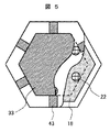
図4は、本発明の一実施形態における超音波送受信デバイスの1個の超音波送受信セル10aの上面の部分分解図である。配線層23は、上部電極18と同様六角形である。貫通配線22は円柱状である。貫通配線の平断面の直径は、5〜6μm程度が好ましい。
FIG. 4 is a partial exploded view of the upper surface of one ultrasonic transmission /
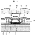
ここで、図11を用いて、配線層23および貫通配線22の設置位置を説明する。特許文献2の図3(b)には、上部電極307と下部電極302に駆動電圧を印加し、電極間に形成されたギャップの変形を利用して、ギャップを取り囲む絶縁膜305、上部電極を取り囲む絶縁膜308、下部電極を取り囲む絶縁膜301を変形させるが、ギャップが小さくなったときに、上部電極の上下にある絶縁膜308,305には応力が発生する。この変形は比較的厚みのある構造体の変形であるため、その厚さ方向の中心部(応力中心面)の上部では圧縮応力場62が、下部では引張応力場61が発生する。
Here, the installation positions of the
上部電極は上下に振動するため、圧縮応力場と引張応力場は、振動にあわせて交互に入れ替わる(図面では、応力中心面の貫通配線の左右)ことになる。また、引張応力場に上部電極及び配線が配置されているため、上部電極の駆動による応力の変動が大きく、電極材の疲労破壊やクリープ変形が発生しやすい。 Since the upper electrode vibrates up and down, the compressive stress field and the tensile stress field alternate with each other according to the vibration (in the drawing, left and right of the through wiring on the stress center plane). In addition, since the upper electrode and the wiring are arranged in the tensile stress field, the fluctuation of the stress due to the driving of the upper electrode is large, and fatigue failure and creep deformation of the electrode material are likely to occur.
図11は、本発明の実施形態による超音波送受信デバイスの構成・作用を説明するための断面略図である。図において、応力中心場63に配線層23を形成しているため、上部電極18の駆動による応力変動が小さく、疲労破壊やクリープ変形の影響を軽減できる。
FIG. 11 is a schematic cross-sectional view for explaining the configuration and operation of the ultrasonic transmission / reception device according to the embodiment of the present invention. In the figure, since the
なお、上部電極18は耐クリープ性の材料が良く、製造プロセスを考慮するとポリシリコンやタングステンが好ましいが、その他の材料、例えばシリコンを添加したチタンなどでも良い。
The
次に、貫通配線22の設置場所を説明する。特許文献2の図3〔b〕に示すように、超音波送受信セルの中央から上下方向に離れた場所付近は、応力変動が大きいため、貫通配線の設置には不適である。そのため、超音波送受信セルの中心から平面方向に離れた場所にも、図11に示すように、引張応力場72と圧縮応力場71が交互に発生する。そのため、貫通配線22は、引張応力場72と圧縮応力場71の中間点73(又は引張応力場72と圧縮応力場71の境界近傍)に形成することが良い。なお、圧縮応力場71と引張応力場72は上部電極18、絶縁膜17、20、配線層23及びギャップ16の変形によって形成される。
Next, the installation place of the
図13は、図11で説明した前記ギャップ上部膜の応力場の状態を模式的に示した図である。ギャップ上部膜が下部電極14側に接近した状態を示しており、応力中心面100に対して、圧縮応力場101、103、引張応力場102、104が発生する。従って、貫通配線23は応力が最も小さい応力の中心位置に存在する。
FIG. 13 is a diagram schematically showing the state of the stress field of the gap upper film described in FIG. The upper gap film is close to the
(実施例2)
図5には、本発明の第2の実施例を示す。配線層33の大きさが、上部電極18よりも小さく、貫通配線22が内接するまで、後退した程度の大きさである。上部電極の駆動に寄与しない配線層を削除した構造である。その結果、配線層や絶縁膜に対する余分な拘束力が無くなり、クリープ疲労が少なくなる。
(Example 2)
FIG. 5 shows a second embodiment of the present invention. The size of the
(実施例3)
図6には、本発明の第3の実施例を示す。配線層34の形状が、貫通配線22を頂点とする六角形である。図5で示した配線層33の不要な部分を更に削除した構造である。この場合も、実施例2と同様な効果が期待できる。
(Example 3)
FIG. 6 shows a third embodiment of the present invention. The shape of the
(実施例4)
図7には、本発明の第4の実施例を示す。配線層35の平断面形状が、円形である。上部電極と上部電極上下の絶縁膜の駆動による変形が均一となりやすい。そのため、駆動によるギャップの変動が安定し、超音波送受信特性も良好となる。
Example 4
FIG. 7 shows a fourth embodiment of the present invention. The cross-sectional shape of the
(実施例5)
図8には、本発明の第5の実施例を示す。図10は、図8のC−C断面図である。配線層35の形状は円形であるが、さらに、貫通配線52がリング状となっている。このため、上部電極の駆動による変形がさらに安定し、超音波送受信特性も良好となる。また、超音波送受信デバイスの製造が容易になる。
(Example 5)
FIG. 8 shows a fifth embodiment of the present invention. 10 is a cross-sectional view taken along the line CC of FIG. The
(実施例6)
図9には、本発明の第6の実施例を示す。貫通配線52はリング状であるが、さらに、配線層36もリング状である。上部電極の駆動に寄与しない部分を全て削除した構造である。
(Example 6)
FIG. 9 shows a sixth embodiment of the present invention. Although the through
以上、本発明の実施の形態を説明したが、本発明の実施形態によれば、上部電極18に信号を伝達し、電力を供給する配線13と配線を兼用している下層電極14との間の第2の絶縁膜の厚みが厚くなるため、絶縁耐圧が向上する効果もある。
As described above, the embodiment of the present invention has been described. According to the embodiment of the present invention, a signal is transmitted to the
1…超音波探触子、10…超音波送受信デバイス、11…シリコン基板、12…第4の絶縁膜、13…配線、14…下部電極、15…第5の絶縁膜、16…ギャップ、17…第1の絶縁膜、18…上部電極、19…第2の絶縁膜、20…第3の絶縁膜、21…保護膜、22…貫通配線、23…配線層、61,102、104…引張応力場、62,101、103…圧縮応力場、63,100…応力中心面。
DESCRIPTION OF
Claims (11)
第3の絶縁膜とが順次積層された積層体を備え、前記下部電極と上部電極との間に電圧を印加するように構成され、前記上部電極と前記配線層とが、貫通配線により電気的に接続された構造を有することを特徴とする超音波送受信デバイス。 Semiconductor substrate, lower electrode, gap, first insulating film, upper electrode, second insulating film, wiring layer,
A laminated body in which a third insulating film is sequentially laminated, and is configured to apply a voltage between the lower electrode and the upper electrode, and the upper electrode and the wiring layer are electrically connected by a through wiring; An ultrasonic transmission / reception device having a structure connected to
半導体基板と、
前記半導体基板より上に設けられた下部電極と、
前記下部電極より上に設けられたギャップと、
前記ギャップの上に設けられた第1の絶縁膜と、
前記第1の絶縁膜よりも上に設けられる上部電極と、
前記上部電極よりも上に設けられた第2の絶縁膜と、
前記第2の絶縁膜の上に設けられた配線層と、
前記配線層の上に設けられた第3の絶縁膜とを備え、
前記上部電極と前記配線層が、貫通配線で接続されていることを特徴とする超音波送受信デバイス。 In an ultrasonic transmission / reception device that transmits / receives ultrasonic waves,
A semiconductor substrate;
A lower electrode provided above the semiconductor substrate;
A gap provided above the lower electrode;
A first insulating film provided on the gap;
An upper electrode provided above the first insulating film;
A second insulating film provided above the upper electrode;
A wiring layer provided on the second insulating film;
A third insulating film provided on the wiring layer,
The ultrasonic transmission / reception device, wherein the upper electrode and the wiring layer are connected by a through wiring.
前記上部電極は、ポリシリコン、タングステンまたはシリコン添加チタンからなることを特徴とする超音波送受信デバイス。 In claim 4 or 5,
The ultrasonic transmission / reception device, wherein the upper electrode is made of polysilicon, tungsten, or silicon-added titanium.
半導体基板と、
前記半導体基板より上に設けられた下部電極と、
前記下部電極より上に設けられたギャップと、
前記ギャップの上に設けられた第1の絶縁膜と、
第1の絶縁膜よりも上に設けられる上部電極と、
前記上部電極よりも上に設けられた第2の絶縁膜と、
前記第2の絶縁膜の上に設けられた配線層と、
前記配線層の上に設けられた第3の絶縁膜とを備え、
前記上部電極と前記配線層を接続する貫通配線を備え、
前記下部電極と前記上部電極とに電圧を与えて上部電極を駆動したときに、前記第2の絶縁膜と前記第3の絶縁膜に発生する応力の中心面近傍に、前記配線層を設けたことを特徴とする超音波送受信デバイス。 In an ultrasonic transmission / reception device that transmits / receives ultrasonic waves,
A semiconductor substrate;
A lower electrode provided above the semiconductor substrate;
A gap provided above the lower electrode;
A first insulating film provided on the gap;
An upper electrode provided above the first insulating film;
A second insulating film provided above the upper electrode;
A wiring layer provided on the second insulating film;
A third insulating film provided on the wiring layer,
A through-wiring connecting the upper electrode and the wiring layer;
The wiring layer is provided in the vicinity of a center plane of stress generated in the second insulating film and the third insulating film when the upper electrode is driven by applying a voltage to the lower electrode and the upper electrode. An ultrasonic transmission / reception device.
前記貫通配線は、前記上部電極に対して垂直方向で、応力の中心となる位置に設けられたことを特徴とする超音波送受信デバイス。 In claim 7,
The ultrasonic transmission / reception device, wherein the through wiring is provided at a position that is a center of stress in a direction perpendicular to the upper electrode.
Priority Applications (3)
| Application Number | Priority Date | Filing Date | Title |
|---|---|---|---|
| JP2007128020A JP4958631B2 (en) | 2007-05-14 | 2007-05-14 | Ultrasonic transmitting / receiving device and ultrasonic probe using the same |
| US12/119,567 US7944114B2 (en) | 2007-05-14 | 2008-05-13 | Ultrasonic transducer device and ultrasonic wave probe using same |
| EP08008864A EP2002900A3 (en) | 2007-05-14 | 2008-05-13 | Ultrasonic transducer device and ultrasonic wave probe using same |
Applications Claiming Priority (1)
| Application Number | Priority Date | Filing Date | Title |
|---|---|---|---|
| JP2007128020A JP4958631B2 (en) | 2007-05-14 | 2007-05-14 | Ultrasonic transmitting / receiving device and ultrasonic probe using the same |
Publications (3)
| Publication Number | Publication Date |
|---|---|
| JP2008283618A JP2008283618A (en) | 2008-11-20 |
| JP2008283618A5 JP2008283618A5 (en) | 2010-04-02 |
| JP4958631B2 true JP4958631B2 (en) | 2012-06-20 |
Family
ID=39730768
Family Applications (1)
| Application Number | Title | Priority Date | Filing Date |
|---|---|---|---|
| JP2007128020A Expired - Fee Related JP4958631B2 (en) | 2007-05-14 | 2007-05-14 | Ultrasonic transmitting / receiving device and ultrasonic probe using the same |
Country Status (3)
| Country | Link |
|---|---|
| US (1) | US7944114B2 (en) |
| EP (1) | EP2002900A3 (en) |
| JP (1) | JP4958631B2 (en) |
Families Citing this family (9)
| Publication number | Priority date | Publication date | Assignee | Title |
|---|---|---|---|---|
| JP4958631B2 (en) * | 2007-05-14 | 2012-06-20 | 株式会社日立製作所 | Ultrasonic transmitting / receiving device and ultrasonic probe using the same |
| JP5409251B2 (en) * | 2008-11-19 | 2014-02-05 | キヤノン株式会社 | Electromechanical transducer and method for manufacturing the same |
| JP5513239B2 (en) * | 2010-04-27 | 2014-06-04 | キヤノン株式会社 | Electromechanical converter and manufacturing method thereof |
| JP5852461B2 (en) * | 2012-02-14 | 2016-02-03 | 日立アロカメディカル株式会社 | Ultrasonic probe and ultrasonic diagnostic apparatus using the same |
| JP6273743B2 (en) | 2013-09-30 | 2018-02-07 | セイコーエプソン株式会社 | Ultrasonic device and probe, electronic apparatus and ultrasonic imaging apparatus |
| JP6381195B2 (en) | 2013-10-22 | 2018-08-29 | キヤノン株式会社 | Capacitance type transducer and manufacturing method thereof |
| WO2017103172A1 (en) * | 2015-12-18 | 2017-06-22 | Koninklijke Philips N.V. | An acoustic lens for an ultrasound array |
| JP6606034B2 (en) * | 2016-08-24 | 2019-11-13 | 株式会社日立製作所 | Capacitive detection type ultrasonic transducer and ultrasonic imaging apparatus including the same |
| CN111766973B (en) * | 2020-06-11 | 2022-02-01 | 武汉华星光电半导体显示技术有限公司 | Touch display panel and display device |
Family Cites Families (19)
| Publication number | Priority date | Publication date | Assignee | Title |
|---|---|---|---|---|
| JPH07121159B2 (en) * | 1985-03-26 | 1995-12-20 | 日本電気株式会社 | Ultrasonic transducer |
| US6271620B1 (en) * | 1999-05-20 | 2001-08-07 | Sen Corporation | Acoustic transducer and method of making the same |
| DE60036210T2 (en) | 1999-05-25 | 2008-05-21 | Fabrizio Monrovia Pinto | METHOD AND DEVICE FOR ENERGY EXTRACTION |
| US20030087292A1 (en) * | 2001-10-04 | 2003-05-08 | Shiping Chen | Methods and systems for promoting interactions between probes and target molecules in fluid in microarrays |
| JP2004247520A (en) * | 2003-02-14 | 2004-09-02 | Matsushita Electric Ind Co Ltd | Semiconductor device |
| EP1725343A2 (en) * | 2004-03-11 | 2006-11-29 | Georgia Technology Research Corporation | Asymmetric membrane cmut devices and fabrication methods |
| US20060004290A1 (en) * | 2004-06-30 | 2006-01-05 | Smith Lowell S | Ultrasound transducer with additional sensors |
| JP4513596B2 (en) * | 2004-08-25 | 2010-07-28 | 株式会社デンソー | Ultrasonic sensor |
| US7489593B2 (en) * | 2004-11-30 | 2009-02-10 | Vermon | Electrostatic membranes for sensors, ultrasonic transducers incorporating such membranes, and manufacturing methods therefor |
| JP4471856B2 (en) * | 2005-01-27 | 2010-06-02 | 株式会社日立製作所 | Ultrasonic transducer and manufacturing method thereof |
| JP4523879B2 (en) * | 2005-06-20 | 2010-08-11 | 株式会社日立製作所 | Electrical / acoustic transducers, array-type ultrasonic transducers and ultrasonic diagnostic equipment |
| JP4682927B2 (en) * | 2005-08-03 | 2011-05-11 | セイコーエプソン株式会社 | Electrostatic ultrasonic transducer, ultrasonic speaker, audio signal reproduction method, ultrasonic transducer electrode manufacturing method, ultrasonic transducer manufacturing method, superdirective acoustic system, and display device |
| JP4434109B2 (en) * | 2005-09-05 | 2010-03-17 | 株式会社日立製作所 | Electrical / acoustic transducer |
| JP4724501B2 (en) * | 2005-09-06 | 2011-07-13 | 株式会社日立製作所 | Ultrasonic transducer and manufacturing method thereof |
| US8397574B2 (en) * | 2005-10-18 | 2013-03-19 | Hitachi, Ltd. | Ultrasonic transducer, ultrasonic probe, and ultrasonic imaging device |
| JP4844411B2 (en) * | 2006-02-21 | 2011-12-28 | セイコーエプソン株式会社 | Electrostatic ultrasonic transducer, method for manufacturing electrostatic ultrasonic transducer, ultrasonic speaker, audio signal reproduction method, superdirective acoustic system, and display device |
| JP4699259B2 (en) * | 2006-03-31 | 2011-06-08 | 株式会社日立製作所 | Ultrasonic transducer |
| JP4800170B2 (en) * | 2006-10-05 | 2011-10-26 | 株式会社日立製作所 | Ultrasonic transducer and manufacturing method thereof |
| JP4958631B2 (en) * | 2007-05-14 | 2012-06-20 | 株式会社日立製作所 | Ultrasonic transmitting / receiving device and ultrasonic probe using the same |
-
2007
- 2007-05-14 JP JP2007128020A patent/JP4958631B2/en not_active Expired - Fee Related
-
2008
- 2008-05-13 EP EP08008864A patent/EP2002900A3/en not_active Withdrawn
- 2008-05-13 US US12/119,567 patent/US7944114B2/en not_active Expired - Fee Related
Also Published As
| Publication number | Publication date |
|---|---|
| US20080284287A1 (en) | 2008-11-20 |
| US7944114B2 (en) | 2011-05-17 |
| EP2002900A2 (en) | 2008-12-17 |
| EP2002900A3 (en) | 2012-05-30 |
| JP2008283618A (en) | 2008-11-20 |
Similar Documents
| Publication | Publication Date | Title |
|---|---|---|
| JP4958631B2 (en) | Ultrasonic transmitting / receiving device and ultrasonic probe using the same | |
| JP4730162B2 (en) | Ultrasonic transmitting / receiving device, ultrasonic probe, and manufacturing method thereof | |
| US20140010052A1 (en) | Capacitive transducer | |
| US9925561B2 (en) | Capacitive micromachined ultrasonic transducer with multiple deflectable membranes | |
| US10101303B2 (en) | Capacitive micromachined ultrasonic transducer and test object information acquiring apparatus including capacitive micromachined ultrasonic transducer | |
| JP4774393B2 (en) | Ultrasonic transducer, ultrasonic diagnostic apparatus and ultrasonic microscope | |
| JP2008099036A (en) | Ultrasonic transducer, ultrasonic probe and ultrasonic diagnostic device | |
| US10350636B2 (en) | Capacitive transducer and sample information acquisition apparatus | |
| WO2015088708A2 (en) | Flexible micromachined transducer device and method for fabricating same | |
| EP2682195A2 (en) | Capacitive transducer | |
| JPWO2012050172A1 (en) | Ultrasonic transducer and ultrasonic diagnostic apparatus using the same | |
| CN101238506A (en) | Wide-bandwidth matrix transducer with polyethylene third matching layer | |
| EP2792423A2 (en) | Transducer, method for manufacturing transducer, and object information acquiring apparatus | |
| JP2009272824A (en) | Ultrasonic wave vibrator cell, ultrasonic wave vibrator, and ultrasonic endoscope | |
| JP2009050560A (en) | Ultrasonic transducer, ultrasonic diagnostic system and ultrasonic microscope | |
| US20160051226A1 (en) | Ultrasonic transducers and methods of manufacturing the same | |
| EP2733961B1 (en) | Ultrasonic element, and ultrasonic endoscope | |
| JP6752727B2 (en) | Ultrasound Transducer and Ultrasound Imaging Device | |
| EP3851164A1 (en) | Ultrasound emission device and ultrasound apparatus | |
| JP2017176769A (en) | Acoustic wave probe and information acquisition device | |
| WO2021125087A1 (en) | Ultrasound device and ultrasonic diagnostic apparatus | |
| US20200041459A1 (en) | Capacitive transducer and ultrasonic probe using same | |
| JP2016063499A (en) | Transducer and analyte information acquisition device | |
| JP2013165473A (en) | Ultrasonic module |
Legal Events
| Date | Code | Title | Description |
|---|---|---|---|
| A521 | Request for written amendment filed |
Free format text: JAPANESE INTERMEDIATE CODE: A523 Effective date: 20100216 |
|
| A621 | Written request for application examination |
Free format text: JAPANESE INTERMEDIATE CODE: A621 Effective date: 20100216 |
|
| A977 | Report on retrieval |
Free format text: JAPANESE INTERMEDIATE CODE: A971007 Effective date: 20111125 |
|
| A131 | Notification of reasons for refusal |
Free format text: JAPANESE INTERMEDIATE CODE: A131 Effective date: 20111206 |
|
| A521 | Request for written amendment filed |
Free format text: JAPANESE INTERMEDIATE CODE: A523 Effective date: 20120131 |
|
| TRDD | Decision of grant or rejection written | ||
| A01 | Written decision to grant a patent or to grant a registration (utility model) |
Free format text: JAPANESE INTERMEDIATE CODE: A01 Effective date: 20120221 |
|
| A01 | Written decision to grant a patent or to grant a registration (utility model) |
Free format text: JAPANESE INTERMEDIATE CODE: A01 |
|
| A61 | First payment of annual fees (during grant procedure) |
Free format text: JAPANESE INTERMEDIATE CODE: A61 Effective date: 20120319 |
|
| FPAY | Renewal fee payment (event date is renewal date of database) |
Free format text: PAYMENT UNTIL: 20150330 Year of fee payment: 3 |
|
| R150 | Certificate of patent or registration of utility model |
Free format text: JAPANESE INTERMEDIATE CODE: R150 |
|
| LAPS | Cancellation because of no payment of annual fees |